WO2018079657A1 - 太陽電池の検査方法および検査装置、太陽電池の製造方法および太陽電池モジュールの製造方法、ならびに検査用プログラムおよび記憶媒体 - Google Patents
太陽電池の検査方法および検査装置、太陽電池の製造方法および太陽電池モジュールの製造方法、ならびに検査用プログラムおよび記憶媒体 Download PDFInfo
- Publication number
- WO2018079657A1 WO2018079657A1 PCT/JP2017/038710 JP2017038710W WO2018079657A1 WO 2018079657 A1 WO2018079657 A1 WO 2018079657A1 JP 2017038710 W JP2017038710 W JP 2017038710W WO 2018079657 A1 WO2018079657 A1 WO 2018079657A1
- Authority
- WO
- WIPO (PCT)
- Prior art keywords
- collector electrode
- solar cell
- inspection
- electrode
- type semiconductor
- Prior art date
- Legal status (The legal status is an assumption and is not a legal conclusion. Google has not performed a legal analysis and makes no representation as to the accuracy of the status listed.)
- Ceased
Links
Images


Classifications
-
- G—PHYSICS
- G01—MEASURING; TESTING
- G01N—INVESTIGATING OR ANALYSING MATERIALS BY DETERMINING THEIR CHEMICAL OR PHYSICAL PROPERTIES
- G01N21/00—Investigating or analysing materials by the use of optical means, i.e. using sub-millimetre waves, infrared, visible or ultraviolet light
- G01N21/84—Systems specially adapted for particular applications
- G01N21/88—Investigating the presence of flaws or contamination
- G01N21/95—Investigating the presence of flaws or contamination characterised by the material or shape of the object to be examined
-
- H—ELECTRICITY
- H02—GENERATION; CONVERSION OR DISTRIBUTION OF ELECTRIC POWER
- H02S—GENERATION OF ELECTRIC POWER BY CONVERSION OF INFRARED RADIATION, VISIBLE LIGHT OR ULTRAVIOLET LIGHT, e.g. USING PHOTOVOLTAIC [PV] MODULES
- H02S50/00—Monitoring or testing of PV systems, e.g. load balancing or fault identification
- H02S50/10—Testing of PV devices, e.g. of PV modules or single PV cells
- H02S50/15—Testing of PV devices, e.g. of PV modules or single PV cells using optical means, e.g. using electroluminescence
-
- Y—GENERAL TAGGING OF NEW TECHNOLOGICAL DEVELOPMENTS; GENERAL TAGGING OF CROSS-SECTIONAL TECHNOLOGIES SPANNING OVER SEVERAL SECTIONS OF THE IPC; TECHNICAL SUBJECTS COVERED BY FORMER USPC CROSS-REFERENCE ART COLLECTIONS [XRACs] AND DIGESTS
- Y02—TECHNOLOGIES OR APPLICATIONS FOR MITIGATION OR ADAPTATION AGAINST CLIMATE CHANGE
- Y02E—REDUCTION OF GREENHOUSE GAS [GHG] EMISSIONS, RELATED TO ENERGY GENERATION, TRANSMISSION OR DISTRIBUTION
- Y02E10/00—Energy generation through renewable energy sources
- Y02E10/50—Photovoltaic [PV] energy
Definitions
- the present invention relates to an electrode inspection method and an inspection apparatus for solar cells. Moreover, this invention relates to the manufacturing method of the solar cell including the electrode test process of the said solar cell, and the manufacturing method of a solar cell module. Furthermore, the present invention relates to an inspection program used for inspecting an electrode of a solar cell, and a storage medium storing the program.
- a collector electrode made of a conductive material such as a metal is formed on a p-type semiconductor and an n-type semiconductor in order to extract optical carriers generated on the semiconductor substrate to an external circuit.
- the collector electrode on the light receiving surface side is formed in a pattern in order to reduce shadowing loss.
- the collector electrode on the back side may also be formed in a pattern.
- a patterned collector electrode is provided only on the back surface side.
- the pattern of the collecting electrode of the double-sided electrode type solar cell is typically in the form of a grid composed of about 2 to 4 thick bus bar electrodes and a large number of thin finger electrodes orthogonal to the bus bar electrodes.
- a comb-like pattern is formed in which a collector electrode on a p-type semiconductor and a collector electrode on an n-type semiconductor mesh with each other.
- a printing technique such as screen printing or photolithography is used.
- the cause of failure can be identified from the measured values such as short circuit current, open circuit voltage, curve factor, IV curve shape, etc.
- the evaluation by the solar simulator measures the bulk characteristics of a module in which one cell or a plurality of cells are connected, so it cannot be specified at which position in the surface of the cell the defect has occurred. . For example, when disconnection occurs due to defective printing of the collector electrode, in the inspection by the solar simulator, disconnection occurs at which position of which finger electrode among tens to hundreds of finger electrodes in one cell. It cannot be specified.
- Imaging inspection by electroluminescence (EL) or photoluminescence (PL) is known as a method capable of specifying a defect occurrence location (for example, Patent Document 1 and Patent Document 2).
- EL inspection EL light emission is observed when a forward bias voltage is applied to the solar cell. Since the emission intensity is reduced at a location where a defect such as an electrode disconnection occurs, it is possible to identify a defective location such as a disconnection by imaging the intensity distribution of EL emission.
- PL inspection In PL inspection, light emission is observed when photocarriers (holes and electrons) generated by irradiating the solar cell with light having energy higher than the band gap of the solar cell are recombined. Since a recombination process is different from a normal location at a location where a defect exists in the semiconductor, a difference occurs in PL emission intensity and emission wavelength observed at a normal location and a defective location. In the PL inspection, it is possible to identify a defective portion related to a semiconductor element such as a crack of a semiconductor substrate, a semiconductor bonding failure, and a dopant concentration distribution.
- JP 2010-171046 A Japanese Patent Laying-Open No. 2015-59781
- ⁇ PL inspection can measure failure modes that cannot be detected by EL inspection. Further, since the PL inspection does not need to apply a voltage to the solar cell, it has an advantage that it can also be applied to a solar cell (photoelectric conversion portion as a diode) before electrode formation. However, the conventional PL inspection cannot detect a disconnection failure of the collector electrode.
- the EL inspection can detect a disconnection failure of the electrode, but requires a power supply facility for applying a forward bias voltage to the solar cell, and it is difficult to say that simplicity and safety are sufficient. Further, in order to increase the detection accuracy of defects, it is necessary to increase the EL emission intensity by applying a high voltage, which may cause electrical breakdown of the cell.
- an object of the present invention is to provide an inspection method capable of detecting a disconnection defect of a collector electrode of a solar cell with high accuracy and high convenience.
- photoluminescence (PL) measurement is performed by irradiating the solar cell with light while the electrode on the p-type semiconductor of the solar cell and the electrode on the n-type semiconductor are electrically connected. To do. Based on the brightness and darkness of the obtained PL image, it is possible to identify the location where the electrode is disconnected. For example, the brightness of the photoluminescence image is confirmed along the extending direction of the collector electrode, and the presence / absence of a bright region having a higher photoluminescence intensity than other portions is confirmed. When a bright area is detected, a light / dark boundary can be identified as a disconnection failure location.
- the solar cell includes a patterned first collector electrode on the first main surface of the photoelectric conversion unit, and a second collector electrode on the second main surface of the photoelectric conversion unit.
- the first main surface is irradiated with light, and the photoluminescence measurement is performed. Based on this, it is possible to identify the disconnection failure location of the first collector electrode.
- the present invention relates to an inspection apparatus used for the above inspection.
- the inspection device electrically connects a light irradiation unit that irradiates light to the main surface of the solar cell, an imaging unit that receives photoluminescence of the solar cell, and the first collector electrode and the second collector electrode of the solar cell.
- the inspection apparatus may further include a data processing unit including a computer for performing data processing of photoluminescence received by the imaging unit.
- the memory of the inspection apparatus may store a program for causing the computer of the data processing unit to execute a process of identifying a disconnection failure location based on the intensity of photoluminescence.
- the process of identifying a disconnection failure location based on the intensity of photoluminescence includes, for example, a step of detecting a change in the intensity of photoluminescence along the extending direction of the collector electrode, and another location along the extending direction of the collector electrode. Outputting a position information of a light / dark boundary when a bright region having a higher photoluminescence intensity than that of is detected.
- the present invention relates to the above-described inspection program and a computer-readable readable storage medium storing the inspection program.
- this invention relates to the manufacturing method of a solar cell including said test process, and the manufacturing method of a solar cell module.
- a photoelectric conversion unit having a first conductivity type semiconductor and a second conductivity type semiconductor is prepared, and a first collector electrode and a second collector electrode are formed on the photoelectric conversion unit, By the above inspection method, the collector electrode is inspected for defective disconnection.
- the disconnection failure location may be specified, and the result may be fed back to the collector electrode formation.
- the result may be fed back to the collector electrode formation.
- a photoelectric conversion unit having a first conductivity type semiconductor and a second conductivity type semiconductor is prepared, and a first collector electrode and a second collector electrode are formed on the photoelectric conversion unit,
- the collector electrode is inspected for disconnection by the above inspection method, and a plurality of solar cells after the inspection are electrically connected.
- Detecting a disconnection failure by PL inspection does not require application of a high voltage as in EL inspection, and thus has the advantage of being excellent in safety and simplicity, and being less susceptible to electrical breakdown of cells.
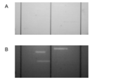
- A is a PL image of a solar cell in an open state
- B is a PL image of a solar cell in a short circuit state.
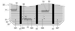
- It is a schematic diagram of the PL image in a short circuit state.
- It is a flowchart which shows an example of PL inspection process.
- the solar cell to be inspected according to the present invention includes a collector electrode on a photoelectric conversion unit including a semiconductor junction between a first conductivity type semiconductor and a second conductivity type semiconductor.
- a first collector electrode is provided on the first conductivity type semiconductor, and a second collector electrode is provided on the second conductivity type semiconductor.
- the first conductivity type semiconductor and the second conductivity type semiconductor have different conductivity types. For example, if the first conductivity type is p-type, the second conductivity type is n-type.
- the solar cell examples include a crystalline silicon solar cell, a crystalline semiconductor solar cell using a semiconductor substrate other than silicon such as GaAs, a silicon thin film solar cell, a compound semiconductor solar cell such as CIS and CIGS, and the like.
- the double-sided electrode type solar cell includes collector electrodes on both surfaces (first main surface and second main surface) of the photoelectric conversion unit, and the collector electrode on at least one surface (first main surface) is formed in a pattern. .
- the collector electrode on at least one surface (first main surface) is formed in a pattern.
- at least a collector electrode on the light-receiving surface side has a pattern shape. Patterned collecting electrodes may be provided on both sides of the photoelectric conversion unit.
- FIG. 1 is a plan view of a crystalline silicon solar cell provided with a patterned collector electrode.
- a solar cell 10 shown in FIG. 1 includes a grid-shaped collector electrode 5 including a plurality of finger electrodes 3 arranged in parallel and a bus bar electrode 4 extending perpendicular to the finger electrodes on the photoelectric conversion unit 1.
- the finger electrode has a line width of about 30 to 200 ⁇ m
- the bus bar electrode has a line width of about 500 to 2000 ⁇ m.
- photocarriers holes and electrons
- electrons are collected at the electrode on the n-type semiconductor
- holes are collected at the electrode on the p-type semiconductor.
- a wiring material is attached to the bus bar electrode 4, and the optical carrier collected by the finger electrodes is taken out to an external circuit through the bus bar electrode and the wiring material.
- the collecting electrode is generally formed of a metal material.
- a conductive material such as carbon may be used.
- Various printing techniques are used to form the patterned collector electrode.
- the metal collector electrode is formed by inkjet, screen printing, spraying, or the like.
- a patterned metal seed is formed, the metal electrode is deposited by plating from the metal seed, and a metal layer is formed by plating on the entire surface of the photoelectric conversion part A method of forming an electrode pattern by etching or the like is employed.
- the metal seed can be formed by printing a conductive paste, photolithography, or the like.
- An insulating layer may be formed on the metal seed, and an electrode may be deposited on the metal seed by plating through an opening provided in the insulating layer (for example, Japanese Patent Application Laid-Open No. 2011-199045, WO 2011/045287, WO2013 / 077038, WO2014 / 097829).
- connection failure including local line thinning
- the extraction efficiency of the photocarrier generated in the photoelectric conversion unit such as a silicon substrate decreases. For this reason, the conversion characteristics of the solar cell are deteriorated.
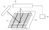
- FIG. 2 is a conceptual diagram showing a state of a disconnection inspection of solar cell electrodes.
- the inspection apparatus includes a conductive member for electrically connecting an electrode on a p-type semiconductor and an electrode on an n-type semiconductor of the solar cell, a light irradiation unit that irradiates light on the main surface of the solar cell, and the solar cell.
- the imaging part which light-receives PL from is provided.
- PL is obtained by recombination of the photocarriers. Luminescence occurs.
- the PL from the solar cell is observed (photographed) by a camera 83 as an imaging means.
- the PL emission intensity information obtained by the camera is processed by the data processing unit 90, whereby a PL emission intensity distribution (PL image) of the inspection target surface is obtained.
- a short-circuit solar cell in which a collector electrode on a p-type semiconductor and a collector electrode on an n-type semiconductor are electrically connected is irradiated with light, and PL emission is observed.
- the solar cell In the short-circuited state, the solar cell can be energized, and light carriers hardly accumulate in the photoelectric conversion part, so that PL light emission is hardly observed.
- the PL emission intensity is extremely small in the short-circuited state compared to the open state, the in-plane emission intensity distribution can be detected by performing long-time exposure (integration) (see FIG. 3B).
- the entire surface to be inspected of the solar cell emits light, and thus a clear difference in brightness is not confirmed.
- the PL emission intensity is generally low, but as shown in FIG. 3B, in the vicinity of the finger electrode disconnection location, along the extending direction of the finger electrode (the left-right direction in the figure) There is a region where the PL emission intensity is larger than the region, and a clear contrast difference is confirmed.
- FIG. 4 is a schematic diagram for explaining a method for identifying a disconnection failure location based on a PL image of a short-circuited solar cell.
- regions hatching regions 71, 72, and 73 having a higher PL emission intensity than other regions.
- the finger electrode 4 is surrounded by the finger electrodes 31, 32 (326) and the bus bar electrodes 42, 43. Since neither the finger electrode surrounding the point D nor the bus bar electrode has a disconnection defect, the carrier is normally recovered.
- the points A, B, and C are surrounded by the finger electrodes 31 and 32 and the bus bar electrodes 41 and 42, and the finger electrode 32 is disconnected at the disconnection location 52, and is divided into the finger electrode 323 and the finger electrode 324. ing.
- the carrier generated at the point B and collected by the finger electrode 324 cannot move to the bus bar electrode 41 existing in the vicinity due to the influence of the disconnection point 52. Since the distance that the carrier moves through the finger electrode 324 is long and the line resistance is large up to the bus bar electrode 42, the carrier is prevented from moving and the carrier is likely to stay.
- the optical carrier tends to stay in the photoelectric conversion portion on the side away from the bus bar electrode at the disconnection part. . Therefore, in PL measurement in a short-circuit state, the PL emission intensity increases due to an increase in carrier recombination, and it is considered that there is a difference in intensity between light and dark along the extending direction of the finger electrode, with the disconnection portion of the finger electrode as a boundary. . In FIG.
- the regions 71, 72, and 73 having higher PL emission intensity than the other regions are detected along the extending direction of the finger electrode, and along the extending direction of the finger electrode.
- the portion where the intensity difference between light and dark is generated can be specified as the disconnection portion of the finger electrode.
- the disconnection failure location (where the disconnection failure occurs in which finger electrode) can be specified by the short-circuit PL inspection.
- the collector electrode on at least one surface may be formed in a pattern.
- the pattern shape is not particularly limited, and may be composed only of finger electrodes extending in parallel, or may be a grid shape composed of finger electrodes and bus bar electrodes.
- the inspection may be performed in a state where a plurality of finger electrodes are electrically connected via a wiring member or the like.
- the inspection target surface may be the light receiving surface or the back surface as long as the collector electrode is formed in a pattern.
- both the light receiving surface and the back surface can be inspected.
- the method for electrically connecting the front and back electrodes of the double-sided electrode type solar cell is not particularly limited, and an appropriate conducting member such as a metal wire may be used.
- an appropriate conducting member such as a metal wire
- a conducting member in which probe pins 21 and 22 are provided at both ends of the conducting wire 25 is used, and the probe pin 21 at one end of the conducting wire 25 is brought into contact with the bus bar electrode 4 on the surface to be inspected.
- the front and back electrodes are short-circuited by bringing the end probe pin 22 into contact with the opposite electrode.
- the conductive member a metal clip or the like that can sandwich the solar cell from the front and back may be used.
- the in-plane potential is preferably uniform.
- the potential difference in the extending direction of the bus bar electrode can be reduced by connecting a plurality of conductive members to one bus bar.
- a solar cell to which a wiring material for connection with another solar cell or an external circuit is connected may be an inspection target.
- the wiring material connected to the electrode on the surface to be inspected and the wiring material connected to the electrode on the opposite surface may be electrically connected by the conductive member. Good.
- the front and back electrodes are electrically connected, they are not necessarily short-circuited (equal potential).
- a power supply capable of applying a forward bias voltage or a reverse bias voltage may be connected between the front and back electrodes.
- the light source 81 as the light irradiation means may be any light source that can irradiate the surface to be inspected of the solar cell 10 with energy higher than the band gap of the solar cell.
- Light source is preferably one capable of irradiating an inspection light (excitation light) L 0 on the entire inspection target surface of the solar cell.
- the light source is preferably aligned with the solar cell so that the entire surface to be inspected can be irradiated with inspection light having a uniform intensity. Positioning can be performed by moving the stage on which the solar cell is placed and changing the position or angle of the light source.
- the camera 83 that receives and shoots the PL light emitted from the solar cell is preferably capable of shooting the entire surface to be inspected of the solar cell.
- the light receiving element is not particularly limited as long as it can convert the received light intensity into an electric signal and transmit it to the data processing unit.
- the camera is preferably aligned with the solar cell.
- the light source 81 and the camera 83 may be configured to perform light irradiation and photographing on the inspection target surfaces of a plurality of solar cells.
- the PL inspection may be performed using a PL inspection apparatus including a light irradiation unit and an imaging unit. That is, the inspection apparatus of the present invention includes a conductive member for electrically connecting the front and back electrodes of a solar cell (or an electrode on a p-type semiconductor and an electrode on an n-type semiconductor) to form a short-circuit state, A combination with a PL inspection device may also be used.
- the inspection is preferably performed in a dark room.
- the inspection time (integrated time) may be adjusted so that a disconnection failure can be detected by the in-plane distribution of the PL emission intensity according to the irradiation light intensity, the PL emission amount, the camera sensitivity, and the like.
- the integrated exposure amount Is preferably increased.
- the exposure time should be 1.5 to 20 times longer than the PL measurement in the open state for the purpose of detecting a semiconductor junction failure or the like. It is preferably 2 to 5 times.
- PL measurement is performed in a short-circuit state in which the front and back electrodes are electrically connected, and the in-plane PL
- the detection sensitivity (exposure) of the camera and the inspection time may be adjusted so that the average value of the emission intensity matches the average value I OC of the PL emission intensity in the open state.
- Measurement may be performed in the same manner as conventional PL measurement, except that the front and back electrodes of the solar cell are electrically connected and the integrated exposure amount is increased.
- the PL measurement may be performed while applying a forward bias voltage or a reverse bias voltage.
- a bias voltage By applying a bias voltage, the overall PL emission intensity can be adjusted.
- the contrast of light and darkness of PL light emission can be adjusted, so that there are cases where the disconnection location based on light and darkness can be specified more accurately.
- the emission intensity data obtained by the camera 83 is transmitted to the data processing unit 90 for image processing.
- a PL image as shown in FIG. 3B is created based on the integrated light quantity. Based on the brightness of the PL image (the magnitude of the PL intensity), the presence or absence of a disconnection failure and the location of the disconnection failure are specified.
- a boundary where the brightness (PL count) of the PL image changes discontinuously along the extending direction of the finger electrode is detected.
- the light / dark boundary may be detected by visual observation of the PL image, or the light / dark boundary may be detected by further data processing of the PL image.
- the brightness of each pixel of the PL image may be binarized into a bright pixel and a dark pixel with a predetermined threshold. In the binarized PL image, if there is a rectangular dark pixel group along the extending direction of the finger electrode, a disconnection failure of the finger electrode occurs at the boundary between the dark pixel group and the bright pixel group.
- the amount of change (inclination) of the PL count number may be obtained along the extending direction of the finger electrode, and a portion where the amount of change exceeds a predetermined threshold may be specified as the position where the finger electrode is disconnected.
- the obtained position information is output as an image or a digitized position coordinate. Identification of the disconnection failure location based on the PL image can be automated by a predetermined program.
- FIG. 5 is a flowchart showing an example of a process for identifying a disconnection failure location by a short-circuit PL measurement.
- an electrode is connected by a conducting member to make a short circuit (S10).
- Light is irradiated from the light irradiation unit to the short-circuited solar cell (S21), PL light is imaged by the imaging unit (S22), and a PL image is formed based on the emission intensity data (S23).
- S21 short-circuited solar cell
- S22 the imaging unit
- S23 emission intensity data
- relative alignment of the light irradiation unit, the imaging unit, and the solar cell may be performed.
- the PL image is divided into a plurality (N) of regions (S30).
- N regions
- a region surrounded by the finger electrodes and the bus bar electrodes constitutes one region.
- a rectangular region surrounded by two adjacent bus bar electrodes and two adjacent finger electrodes becomes one region.
- one bus bar electrode and a rectangular region surrounded by the peripheral edge of the solar cell and the two finger electrodes form one region.
- the collector electrode has two bus bar electrodes and 100 finger electrodes
- the number of regions N may be set according to the inspection range.
- the presence or absence of a bright region is determined from the distribution of the PL count number along the extending direction of the finger electrode (S33). As described above, the presence of a bright region can be confirmed based on the presence or absence of a light / dark boundary when the brightness of each pixel of the PL image is scanned along the extending direction of the finger electrode. If there is a bright region, the position information of the boundary between the light and dark, for example, the coordinates of the position corresponding to the broken position of the finger electrode is stored in the storage unit as the position information (S36).
- the coordinates stored in the storage unit are output as disconnection failure position information (S39).
- the coordinates may be output as numerical values, or may be output as an image obtained by superimposing the disconnection failure position information on the PL image.
- the processing of S30 to S36 may be executed using a disconnection failure detection program in which processing procedures for determining whether there is a bright area in each area and outputting position information are described.
- the program causes the computer of the data processing unit to execute the step of detecting the intensity change of the photoluminescence along the extending direction of the electrode and the step of outputting the position information of the light / dark boundary along the extending direction of the electrode.
- the computer of the data processing unit may be the same as a computer for controlling light irradiation, imaging, and PL image acquisition.
- the disconnection failure detection program may be provided together with the inspection device in a state stored in the memory.
- the disconnection failure detection program may be provided by being stored in a computer-readable readable storage medium, or may be provided from an external server or the like via an electric communication circuit or the like.
- a program stored in a storage medium, an external server, or the like may be stored in a memory of the inspection apparatus and used.
- the collector electrode may be a comb-like pattern in which a plurality of finger electrodes are connected to one bus bar electrode.
- the disconnection failure occurs in the finger electrode in the comb-shaped pattern collector electrode, the carrier stays more easily in the region farther from the bus bar electrode than the disconnection failure portion. Therefore, in the short-circuit PL inspection, a bright region is observed along the finger electrode in a region farther from the bus bar electrode than the disconnection failure portion.
- the present invention is also applicable to a solar cell having a metal collector electrode only on one main surface, such as a back contact solar cell.
- a solar cell having a metal collector electrode only on one main surface such as a back contact solar cell.
- the electrode on the n-type semiconductor and the electrode on the p-type semiconductor provided on the back surface are connected to each other by a conducting member and short-circuited.
- Light is irradiated from the light receiving surface side in a short circuit state, and a PL image of the light receiving surface is acquired.
- the PL image and the pattern shape of the electrode are collated to identify the disconnection defective portion of the electrode formed on the back surface. That's fine.
- the disconnection failure location can be identified by superimposing the electrode pattern shape on the PL image by image processing.
- the inspection method of the present invention can be used for quality control and process management of solar cells. According to the inspection method of the present invention, not only the occurrence of disconnection failure but also the location of occurrence can be specified, and the cause of failure such as printing failure can be easily identified by feeding back the result to the electrode forming process. . Since it is easy to identify the cause of the failure, it is easy to eliminate the disconnection failure in the manufacturing process of the solar cell, and it is possible to suppress the recurrence of defective products due to the disconnection failure and improve the yield.
- a solar cell module is obtained by connecting and sealing a plurality of solar cells via a wiring material such as a tab wire. You may use the solar cell after test
- a solar cell module that is determined to be a non-defective product in the disconnection defect inspection may be selected and only the non-defective product electrically connected. As described above, by selecting only the solar cells determined to be non-defective and performing electrical connection, it is possible to obtain a high-output solar cell module with a high yield.
- the criteria for determining whether the product is a non-defective product or a defective product may be appropriately set according to the required characteristics. For example, what is necessary is just to determine that the number of disconnection failure locations is a predetermined value or less based on the number of disconnection failure locations. In addition, ranking (numericalization based on the number of points) may be performed in accordance with the disconnection failure location and the type of disconnection failure (for example, the intensity difference between light and dark in the PL image). When there are a plurality of disconnection failure locations, the points of the respective disconnection failure locations may be added together, and the sum of the points being a predetermined value or less may be determined as a non-defective product.
Landscapes
- Physics & Mathematics (AREA)
- Health & Medical Sciences (AREA)
- Life Sciences & Earth Sciences (AREA)
- Chemical & Material Sciences (AREA)
- Analytical Chemistry (AREA)
- Biochemistry (AREA)
- General Health & Medical Sciences (AREA)
- General Physics & Mathematics (AREA)
- Immunology (AREA)
- Pathology (AREA)
- Photovoltaic Devices (AREA)
Abstract
本発明は、第一導電型半導体および第二導電型半導体を有する光電変換部(1)と、第一導電型半導体上の第一集電極と、第二導電型半導体上の第二集電極とを備える太陽電池の検査方法に関し、第一集電極と第二集電極とが導通部材(21,22,25)を介して電気的に接続された状態で、光電変換部に光を照射して、フォトルミネッセンス測定を実施する。得られたフォトルミネッセンス像の明暗に基づいて、集電極の断線不良箇所が特定される。
Description
本発明は、太陽電池の電極の検査方法、および検査装置に関する。また、本発明は、当該太陽電池の電極検査工程を含む太陽電池の製造方法および太陽電池モジュールの製造方法に関する。さらに、本発明は、太陽電池の電極の検査に用いられる検査用プログラム、および当該プログラムが格納された記憶媒体に関する。
結晶シリコン等の半導体基板を用いた太陽電池では、半導体基板で生成した光キャリアを外部回路に取り出すために、p型半導体上およびn型半導体上に、金属等の導電性材料からなる集電極が設けられている。両面電極型太陽電池では、シャドーイングロスを低減するために、受光面側の集電極はパターン状に形成されている。裏面側の集電極もパターン状に形成される場合がある。バックコンタクト型太陽電池では、裏面側にのみパターン状の集電極が設けられている。
両面電極型太陽電池の集電極のパターンは、典型的には、2~4本程度の太いバスバー電極と、バスバー電極に直交する多数の細いフィンガー電極とからなるグリッド状である。バックコンタクト型太陽電池では、典型的には、p型半導体上の集電極とn型半導体上の集電極とが互いに噛み合う櫛歯形状のパターンを形成している。パターン状の電極の形成には、スクリーン印刷やフォトリソグラフィー等の印刷技術が用いられる。
太陽電池の製造工程では、種々の検査による品質管理や工程管理が行われている。検査結果に基づいて不良発生原因となっている工程を特定し、不良発生原因を取り除くことにより、不良品の発生を抑制し、歩留まりを向上するとともに、品質を維持できる。例えば、集電極の形成が不良原因と特定された場合は、電極の印刷プロセスを確認し、不良発生原因を除去すればよい。
品質管理として一般的に実施されているソーラーシミュレータによる検査では、短絡電流、開放電圧、曲線因子等の測定値や、I-V曲線の形状等から不良発生原因を特定できる。一方、ソーラーシミュレータによる評価は、1つのセルや複数のセルが接続されたモジュールのバルク特性を測定しているため、セルの面内のどの位置に不良が発生しているかを特定することはできない。例えば、集電極の印刷不良により断線が生じている場合、ソーラーシミュレータによる検査では、1つのセルに数十~数百本存在するフィンガー電極の中の、どのフィンガー電極のどの位置で断線が生じているかを特定することはできない。
断線等の不良箇所を特定するための検査方法として、高解像度カメラで撮影を行い、断線箇所を自動診断する方法が知られている。しかし、この方法は一度に測定できる面積が限定的であり、簡便性に欠ける。
不良発生箇所を特定可能な方法として、エレクトロルミネッセンス(EL)やフォトルミネッセンス(PL)によるイメージング検査が知られている(例えば、特許文献1および特許文献2)。EL検査では、太陽電池に順バイアス電圧を印加した際のEL発光を観察する。電極の断線等の不具合が生じている箇所では発光強度が低下するため、EL発光の強度分布をイメージングすることにより、断線等の不良箇所を特定できる。
PL検査では、太陽電池のバンドギャップよりも高エネルギーの光を太陽電池に照射することにより生じた光キャリア(正孔および電子)が再結合する際の発光を観察する。半導体に欠陥が存在する箇所では正常箇所とは再結合過程が異なるため、正常箇所と不良箇所では観察されるPL発光強度や発光波長に差が生じる。PL検査では、半導体基板のクラック、半導体の接合不良、ドーパントの濃度分布等の半導体素子に関わる不良箇所を特定できる。
PL検査は、EL検査では検知できない不良モードを測定可能である。また、PL検査は太陽電池に電圧を印加する必要がないため、電極形成前の太陽電池(ダイオードとしての光電変換部)にも適用可能であるとの利点を有する。しかしながら、従来のPL検査では、集電極の断線不良を検出できない。
EL検査は、電極の断線不良を検出できるが、太陽電池に順バイアス電圧を印加するための電源設備が必要であり、簡便性や安全性が十分とは言い難い。また、不良の検出精度を高めるためには高電圧を印加してEL発光強度を大きくする必要があり、セルの電気的破壊を生じる場合がある。
上記に鑑み、本発明は、高精度で簡便性が高く、太陽電池の集電極の断線不良を検出可能な検査方法の提供を目的とする。
本発明の検査方法では、太陽電池のp型半導体上の電極とn型半導体上の電極とを電気的に接続した状態で、太陽電池に光を照射して、フォトルミネッセンス(PL)測定を実施する。得られたPL像の明暗に基づいて、電極の断線不良箇所を特定できる。例えば、集電極の延在方向に沿ってフォトルミネッセンス像の明暗を確認し、他の箇所に比べてフォトルミネッセンス強度の大きい明領域の有無を確認する。明領域が検出された場合は、明暗の境界を断線不良箇所として特定することができる。
一実施形態において、太陽電池は、光電変換部の第一主面上にパターン状の第一集電極を備え、光電変換部の第二主面上に第二集電極を備える。この太陽電池の第一集電極と第二集電極とを電気的に接続した状態で、第一主面に光を照射して、フォトルミネッセンス測定を実施し、得られたフォトルミネッセンス像の明暗に基づいて、第一集電極の断線不良箇所を特定できる。
さらに、本発明は上記の検査に用いられる検査装置に関する。検査装置は、太陽電池の主面に光を照射する光照射部と、太陽電池のフォトルミネッセンスを受光する撮像部と、太陽電池の第一集電極と第二集電極とを電気的に接続するための導通部材とを備える。検査装置は、さらに、撮像部で受光したフォトルミネッセンスのデータ処理を行うためのコンピュータを備えるデータ処理部を含んでいてもよい。検査装置のメモリには、フォトルミネッセンスの強度に基づいて断線不良箇所を特定する処理を、データ処理部のコンピュータに実行させるためのプログラムが格納されていてもよい。
フォトルミネッセンスの強度に基づいて断線不良箇所を特定する処理は、例えば、集電極の延在方向に沿ってフォトルミネッセンスの強度変化を検出するステップ、および集電極の延在方向に沿った他の箇所に比べてフォトルミネッセンス強度の大きい明領域が検出された場合に、明暗の境界の位置情報を出力するステップ、を含む。
さらに、本発明は、上記の検査用プログラム、および検査用プログラムが格納されたコンピュータ読み取り可能な可読記憶媒体に関する。
さらに、本発明は、上記の検査工程を含む太陽電池の製造方法および太陽電池モジュールの製造方法に関する。太陽電池の製造方法の一実施形態においては、第一導電型半導体および第二導電型半導体を有する光電変換部を準備し、光電変換部上に第一集電極および第二集電極を形成し、上記の検査方法により、集電極の断線不良の検査が行われる。
上記検査において断線不良が検出された場合には、その断線不良箇所を特定し、その結果を集電極の形成にフィードバックしてもよい。検査結果を集電極の形成工程にフィードバックすることにより、断線不良の発生箇所を特定し、断線不良を解消することが可能となる。
太陽電池モジュールの製造方法の一実施形態では、第一導電型半導体および第二導電型半導体を有する光電変換部を準備し、光電変換部上に第一集電極および第二集電極を形成し、上記の検査方法により集電極の断線不良の検査を行い、検査後の太陽電池の複数を電気的に接続する。断線不良検査結果に基づいて太陽電池の選別を行い、良品と判定された太陽電池のみを電気的に接続して太陽電池モジュールを形成することにより、高出力の太陽電池モジュールを高い歩留まりで得ることが可能となる。
PL検査による断線不良の検出は、EL検査のような高電圧の印加を必要としないため、安全性および簡便性に優れることに加えて、セルの電気的破壊が生じ難いとの利点を有する。
本発明の検査対象となる太陽電池は、第一導電型半導体と第二導電型半導体との半導体接合を含む光電変換部上に集電極を備える。第一導電型半導体上には第一集電極が設けられ、第二導電型半導体上には第二集電極が設けられる。第一導電型半導体と第二導電型半導体は異なる導電型を有する。例えば、第一導電型がp型であれば第二導電型はn型である。
太陽電池の種類としては、結晶シリコン太陽電池、GaAs等のシリコン以外の半導体基板を用いた結晶半導体太陽電池、シリコン系薄膜太陽電池、CIS,CIGS等の化合物半導体太陽電池等が挙げられる。
両面電極型太陽電池は、光電変換部の両面(第一主面および第二主面)に集電極を備え、少なくとも一方の面(第一主面)の集電極がパターン状に形成されている。一般的な両面電極型太陽電池は、少なくとも受光面側の集電極がパターン状である。光電変換部の両面にパターン状の集電極が設けられていてもよい。
図1は、パターン状の集電極を備える結晶シリコン太陽電池の平面図である。図1に示す太陽電池10は、光電変換部1上に、平行に並んだ複数のフィンガー電極3、およびフィンガー電極に直交して延在するバスバー電極4からなるグリッド状の集電極5を備える。フィンガー電極の線幅は30~200μm程度であり、バスバー電極の線幅は500~2000μm程度である。
光電変換部1に光が照射されると、光キャリア(正孔および電子)が生成し、電子はn型半導体上の電極で回収され、正孔はp型半導体上の電極で回収される。グリッド状の集電極を備える太陽電池は、バスバー電極4に配線材が取り付けられ、フィンガー電極で回収された光キャリアは、バスバー電極および配線材を介して外部回路に取り出される。
集電極は一般には金属材料により形成される。集電極の材料として、カーボン等の導電性材料を用いてもよい。パターン状の集電極の形成には、各種の印刷技術が用いられる。例えば、導電性ペーストを用いる場合は、インクジェット、スクリーン印刷、スプレー等により金属集電極が形成される。めっき法により金属集電極を形成する場合、パターン状の金属シードを形成し、金属シードを起点としてめっき法により金属電極を析出させる方法、光電変換部上の全面にめっき法により金属層を形成後、エッチングにより電極パターンを形成する方法等が採用される。金属シードは、導電性ペーストの印刷や、フォトリソグラフィー法等により形成できる。金属シード上に絶縁層を形成し、絶縁層に設けられた開口を介して、めっき法により金属シード上に電極を析出させてもよい(例えば、特開2011-199045号、WO2011/045287号、WO2013/077038号、WO2014/097829号)。
印刷版の目詰まりや、フォトリソグラフィーでの局所的な露光・現像不良等が生じると、電極の断線や、局所的に電極の線幅が細く高抵抗化した部分が生じる。特に、フィンガー電極は、線幅が30~200μm程度と小さいため、断線や局所的な線細りによる高抵抗化が発生しやすい。このような集電極の形成不良(以下では、局所的な線細りも含めて「断線不良」と記載する)が生じると、シリコン基板等の光電変換部で生成した光キャリアの取り出し効率が低下するため、太陽電池の変換特性が低下する。
図2は、太陽電池の電極の断線検査の様子を表す概念図である。検査装置は、太陽電池のp型半導体上の電極とn型半導体上の電極とを電気的に接続するための導通部材と、太陽電池の主面に光を照射する光照射部と、太陽電池からのPLを受光する撮像部を備える。
導通部材により太陽電池の表裏の電極を短絡させた状態で、光照射手段としての光源81から太陽電池10の電極形成面(検査対象面)に光を照射すると、光キャリアの再結合により、PL発光が生じる。太陽電池からのPLを、撮像手段としてのカメラ83により観察(撮影)する。カメラで得られたPL発光強度情報が、データ処理部90で処理されることにより、検査対象面のPL発光強度分布(PL像)が得られる。
一般的なPL検査では、開放状態の太陽電池に光照射が行われる。開放状態で光を照射すると、光キャリアが外部に移動できずに光電変換部内に蓄積するため、キャリア再結合によるPL発光が生じる(図3A参照)。すなわち開放状態のPL検査では、集電極が電極として機能しておらず、半導体基板のクラック、半導体の接合不良、ドーパントの濃度分布等の光電変換部の状態の相違がPL発光強度の相違として観察される。
本発明では、p型半導体上の集電極とn型半導体上の集電極とを電気接続した短絡状態の太陽電池に光照射を行い、PL発光を観察する。短絡状態では、太陽電池が通電可能であり、光電変換部に光キャリアが蓄積し難いため、PL発光はほとんど観察されない。短絡状態は、開放状態に比べるとPL発光強度が極めて小さいものの、長時間の露光(積算)を行えば、面内の発光強度の分布を検出できる(図3B参照)。
図3Aに示すように、開放状態では、太陽電池の検査対象面の全面が発光するため明確な明暗の差が確認されない。一方、短絡状態では、全体的にPL発光強度が小さいが、図3Bに示すように、フィンガー電極の断線箇所の近傍に、フィンガー電極の延在方向(図の左右方向)に沿って、他の領域に比してPL発光強度の大きい領域が存在し、明確なコントラスト差が確認される。
図4は、短絡状態の太陽電池のPL像に基づく断線不良箇所の特定方法を説明するための模式図である。フィンガー電極の断線箇所51,52,53の近傍には、他の領域に比してPL発光強度の大きい領域(ハッチング領域71,72,73)が存在する。
図4の点Dは、フィンガー電極31,32(326)、およびバスバー電極42,43に囲まれている。点Dを囲むフィンガー電極およびバスバー電極は、いずれも断線不良が生じていないため、キャリアは正常に回収される。点A,点Bおよび点Cは、フィンガー電極31,32、およびバスバー電極41,42に囲まれており、フィンガー電極32が断線箇所52で断線して、フィンガー電極323とフィンガー電極324に分断されている。
断線箇所52よりもバスバー電極41に近い側に存在する点Aで生成した光キャリアの大半は、フィンガー電極31およびフィンガー電極323により回収される。断線が生じていないフィンガー電極31で回収されたキャリアは、バスバー電極41およびバスバー電極42に移動する。点Aはバスバー電極42からの距離が遠いため、点Aで生成してフィンガー電極31で回収されたキャリアの大半はバスバー電極41に移動する。フィンガー電極323で回収されたキャリアは、バスバー電極42には移動できず、バスバー電極41にのみ移動する。点Aは、バスバー電極41との距離が小さく、バスバー電極42との距離が大きいため、断線が生じていない場合でも、点Aで生成したキャリアの大半はバスバー電極41に移動する。そのため、断線箇所52の存在により、フィンガー電極323で回収されたキャリアがバスバー電極42に移動できないとしても、その影響は小さく、キャリアの滞留は生じ難い。
断線箇所52よりもバスバー電極42に近い側に存在する点Bおよび点Cで生成したキャリアの大半は、フィンガー電極31およびフィンガー電極324により回収される。バスバー電極42の近傍に位置する点Cでは、断線箇所52の発生の有無にかかわらず、フィンガー電極で回収されたキャリアの大半はバスバー電極42に移動するため、断線箇所52の存在に起因するキャリアの滞留は生じ難い。
一方、点Bで生成してフィンガー電極324で回収されたキャリアは、断線箇所52の影響により、近傍に存在するバスバー電極41には移動できない。バスバー電極42まではフィンガー電極324をキャリアが移動する距離が長くライン抵抗が大きいため、キャリアの移動が妨げられ、キャリアが滞留しやすくなる。
このように、フィンガー電極の断線不良箇所では、フィンガー電極からバスバー電極へのキャリアの移動が阻害されるため、断線箇所のバスバー電極から離れている側では、光キャリアが光電変換部に滞留しやすい。そのため、短絡状態のPL測定では、キャリア再結合の増大により、PL発光強度が大きくなり、フィンガー電極の断線箇所を境界として、フィンガー電極の延在方向に沿って明暗の強度差が生じると考えられる。図4において、断線箇所52の近傍では、断線箇所52からフィンガー電極の延在方向に沿ってバスバー電極41に近い側が暗領域、バスバー電極41から離れている側(バスバー電極42側)が明領域72となる。
このように、短絡状態のPL検査では、フィンガー電極の延在方向に沿って、他の領域に比べてPL発光強度が大きい領域71,72,73が検出され、フィンガー電極の延在方向に沿って明暗の強度差が生じている部分をフィンガー電極の断線箇所として特定できる。すなわち、短絡状態のPL検査により、断線不良箇所(どのフィンガー電極のどの位置に断線不良が発生しているか)を特定できることが分かる。
以下では、太陽電池の電極の断線不良を検出するためのPL検査の実施形態について説明する。
前述のように、両面電極型太陽電池は、少なくとも一方の面の集電極がパターン状に形成されていればよい。パターン形状は特に限定されず、平行に延在するフィンガー電極のみからなるものでもよく、フィンガー電極とバスバー電極とからなるグリッド状でもよい。フィンガー電極のみを有する太陽電池が検査対象の場合は、配線材等を介して複数のフィンガー電極を電気的に接続した状態で検査を行えばよい。
検査の対象面は、集電極がパターン状に形成されていれば、受光面でも裏面でもよい。受光面および裏面の両方にパターン状の集電極を有する太陽電池では、受光面および裏面の両方が検査対象となり得る。
両面電極型太陽電池の表裏の電極を電気的に接続する方法は特に限定されず、金属線等の適宜の導通部材を用いればよい。図2に示す形態では、導線25の両端にプローブピン21,22が設けられた導通部材を用い、導線25の一端のプローブピン21を検査対象面のバスバー電極4に接触させ、導線25の他端のプローブピン22を反対面の電極に接触させることにより、表裏の電極を短絡させている。導線の先端にプローブピンが設けられることにより、導通部材とバスバー電極との接触面積を増大させ、電極間の電気的接続を確実に実施できる。導通部材として、太陽電池を表裏から挟持可能な金属クリップ等を用いてもよい。
フィンガー電極3からバスバー電極4へのキャリアの移動およびバスバー電極4から導通部材へのキャリアの流れを促進し、正常部位での光キャリアの滞留を抑制する観点から、図2に示すように、複数のバスバー電極4のそれぞれに、プローブピン21等の導通部材を接触させることが好ましい。PL発光強度を面内で均一とする観点から、面内の電位が均一であることが好ましい。例えば、1本のバスバーに複数の導通部材を接続することにより、バスバー電極の延在方向での電位差を低減できる。
他の太陽電池や外部回路との接続のための配線材が接続された太陽電池を検査対象としてもよい。配線材が接続された太陽電池が検査対象である場合は、検査対象面の電極に接続された配線材と、反対面の電極に接続された配線材とを、導通部材により電気接続してもよい。表裏の電極は電気的に接続されていれば、必ずしも短絡状態(等電位)である必要はない。例えば、表裏の電極間に順バイアス電圧または逆バイアス電圧を印加可能な電源が接続されていてもよい。
光照射手段としての光源81は、太陽電池10の検査対象面に、太陽電池のバンドギャップよりも高エネルギーの光を照射できるものであればよい。光源は、太陽電池の検査対象面全体に検査光(励起光)L0を照射できるものが好ましい。光源は、検査対象面の全体に均一な強度の検査光を照射できるように、太陽電池との相対的な位置合わせを行うことが好ましい。太陽電池を載置したステージの移動や、光源の位置または角度を変更することにより、位置合わせを実施できる。
太陽電池のPL発光を受光して撮影するカメラ83は、太陽電池の検査対象面の全体を撮影できるものが好ましい。受光素子は、受光強度を電気信号に変換して、データ処理部に送信できるものであれば特に限定されない。光源と同様、カメラも太陽電池との相対的な位置合わせを行うことが好ましい。光源81およびカメラ83は、複数の太陽電池の検査対象面に、光照射および撮影を行うように構成されていてもよい。
光照射部および撮像部を備えるPL検査装置を用いてPL検査を実施してもよい。すなわち、本発明の検査装置は、太陽電池の表裏の電極(またはp型半導体上の電極とn型半導体上の電極)を電気的に接続して短絡状態とするための導通部材と、公知のPL検査装置とを組み合わせたものでもよい。
短絡状態のPLは発光強度が小さいため、検査は暗室で実施することが好ましい。検査時間(積算時間)は、照射光強度、PL発光量、カメラの感度等に応じて、PL発光強度の面内分布により断線不良を検出できるように調整すればよい。太陽電池を開放状態として検査を実施する一般的なPL測定に比べて、太陽電池の表裏の電極を電気的に接続した状態でPL測定を行う場合は、PL発光強度が小さいため、積算露光量を大きくすることが好ましい。例えば、露光時間を長くすることにより積算露光量を大きくする場合、半導体の接合不良の検出等を目的とする開放状態でのPL測定に比べて、露光時間を1.5~20倍とすることが好ましく、2~5倍とすることがより好ましい。
短絡状態のPL測定における積算露光量は、開放状態のPL測定と同等になるように調整すればよい。例えば、開放状態でPL測定を行い、検査対象面全面のPL発光強の平均値IOCを算出した後、表裏の電極を電気的に接続した短絡状態でPL測定を実施し、面内のPL発光強度の平均値が、開放状態でのPL発光強度の平均値IOCに一致するように、カメラの検出感度(露光)や、検査時間を調整すればよい。太陽電池の表裏の電極を電気的に接続すること、および積算露光量を増大させること以外は、従来のPL測定と同様にして測定を実施すればよい。
前述のように、表裏の電極間に電源が接続されている場合は、順バイアス電圧または逆バイアス電圧を印加しながらPL測定を実施してもよい。バイアス電圧を印加することにより、全体のPL発光強度の大小を調整できる。例えば、印加電圧を調整することにより、PL発光の明暗のコントラストを調整できるため、より正確に明暗に基づく断線箇所を特定できる場合がある。
カメラ83で得られた発光強度のデータは、データ処理部90に送信され、画像処理が行われる。データ処理部では、積算光量に基づいて、図3Bに示すようなPL像が作成される。このPL像の明暗(PL強度の大小)に基づいて断線不良の有無、および断線不良箇所の特定が行われる。
前述のように、フィンガー電極に断線不良が生じている場合は、フィンガー電極の延在方向に沿ってPL像の明暗(PLカウント数)が不連続に変化する境界が検出される。PL像の目視により明暗の境界を検出してもよく、PL像をさらにデータ処理して明暗の境界を検出してもよい。データ処理を行う場合は、例えば、PL像の各画素の明度を、所定の閾値で明画素と暗画素とに二値化してもよい。二値化処理を行ったPL像において、フィンガー電極の延在方向に沿った矩形状の暗画素群が存在する場合は、暗画素群と明画素群の境界部分を、フィンガー電極の断線不良発生位置として特定できる。また、フィンガー電極の延在方向に沿ってPLカウント数の変化量(傾き)を求め、変化量が所定の閾値を超える部分をフィンガー電極の断線不良発生位置として特定してもよい。得られた位置情報は、画像または数値化した位置座標として出力される。PL像に基づく断線不良箇所の特定は、所定のプログラムにより自動化することもできる。
図5は、短絡状態のPL測定による断線不良箇所の特定プロセスの一例を示すフローチャートである。まず、導通部材により電極を接続して短絡状態とする(S10)。短絡状態の太陽電池に光照射部から光を照射し(S21)、撮像部によりPL光を撮像し(S22)、発光強度のデータに基づいてPL像が形成される(S23)。短絡状態とした太陽電池に光を照射する前に、光照射部、撮像部および太陽電池の相対的な位置合わせを行ってもよい。
PL像に基づく断線不良箇所の特定においては、まず、PL像を複数(N個)の領域に分割する(S30)。例えば、バスバー電極およびフィンガー電極からなるグリッド状の集電極が形成されている場合には、フィンガー電極とバスバー電極に囲まれた領域が1つの領域を構成する。具体的には、隣接する2本のバスバー電極および隣接する2本のフィンガー電極に囲まれた矩形領域が1つの領域となる。太陽電池の面内の端部では、1本のバスバー電極および太陽電池の周縁と2本のフィンガー電極とに囲まれた矩形領域が1つの領域を形成する。例えば、集電極が2本のバスバー電極および100本のフィンガー電極を有する場合は、太陽電池の主面が3×101=303の領域に分割される。太陽電池の所定の領域の断線不良を検査する場合は、検査範囲に応じて領域数Nを設定すればよい。
n番目の領域(nは1~Nの自然数)において、フィンガー電極の延在方向に沿ったPLカウント数の分布から、明領域の有無を判定する(S33)。前述のように、PL像の各画素の明度をフィンガー電極の延在方向に沿って走査した際の明暗境界の有無に基づいて、明領域の存在を確認できる。明領域が存在する場合は、明暗の境界の位置情報、例えば、フィンガー電極の断線不良箇所に対応する位置の座標を、位置情報として記憶部に記憶させる(S36)。
検査対象のN個の領域の全てについて、明領域の有無の判定および明暗境界の座標の記憶を行った後、記憶部に記憶された座標を、断線不良位置情報として出力する(S39)。座標は数値として出力してもよく、断線不良位置情報をPL像に重ね合わせた画像として出力してもよい。
S30~S36の処理は、各領域の明領域の有無の判定および位置情報の出力を実行させるための処理手順が記述された断線不良検出プログラムを用いて実行してもよい。当該プログラムは、データ処理部のコンピュータに、電極の延在方向に沿ってフォトルミネッセンスの強度変化を検出するステップ、および明暗の境界の位置情報を出力するステップを、データ処理部のコンピュータに実行させる。データ処理部のコンピュータは、光照射、撮像およびPL像取得を制御するためのコンピュータと同一であってもよい。断線不良検出プログラムは、メモリに格納された状態で検査装置とともに提供されてもよい。断線不良検出用プログラムは、コンピュータ読み取り可能な可読記憶媒体に格納して提供されてもよく、外部のサーバ等から電気通信回路等を介して提供されてもよい。記憶媒体や外部のサーバ等に格納されたプログラムを、検査装置のメモリに格納して使用してもよい。
以上、少なくとも一方の主面にグリッド状の集電極が設けられた両面電極型太陽電池におけるフィンガー電極の断線不良を検査する場合を中心に説明したが、電極のパターン形状は必ずしもグリッド状である必要はない。例えば、集電極は、1本のバスバー電極に複数のフィンガー電極が接続された櫛歯状のパターンであってもよい。櫛歯状のパターン集電極においてフィンガー電極に断線不良が生じていると、断線不良箇所よりもバスバー電極から離れた領域は、キャリアの滞留が生じやすい。そのため、短絡状態のPL検査では、断線不良箇所よりもバスバー電極から離れた領域で、フィンガー電極に沿って明領域が観察される。
本発明はバックコンタクト型太陽電池等の一方の主面にのみ金属集電極を備える太陽電池にも適用可能である。バックコンタクト型太陽電池の断線不良の検出においては、まず、裏面に設けられたn型半導体上の電極とp型半導体上の電極とを、導通部材により接続して短絡させる。短絡状態で受光面側から光を照射し、受光面のPL像を取得する。
裏面に形成された電極に断線不良が生じていれば、キャリアの滞留に起因して、受光面のPL像に、電極の延在方向に沿った明領域が観察される。受光面のPL像では、裏面に形成された電極の形状を直接観察することはできないため、PL像と電極のパターン形状とを照合して、裏面に形成された電極の断線不良箇所を特定すればよい。例えば、画像処理により、PL像に電極のパターン形状を重ね合わせることにより、断線不良箇所を特定できる。
本発明の検査方法は、太陽電池の品質管理や工程管理等に利用できる。本発明の検査方法によれば、断線不良の発生の有無だけでなく、発生箇所を特定できるため、その結果を電極形成工程にフィードバックすることにより、印刷不良等の不良発生原因を容易に特定できる。不良発生原因特定が容易であるため、太陽電池の製造工程における断線不良の解消も容易であり、断線不良による不良品の再発を抑制し、歩留まりを向上できる。
複数の太陽電池をタブ線等の配線材を介して接続し、封止することにより、太陽電池モジュールが得られる。本発明の検査方法により検査後の太陽電池を、太陽電池モジュールの製造に用いてもよい。断線不良検査において良品と判定された太陽電池を選別して、良品のみを電気的に接続して太陽電池モジュールを作製してもよい。このように、良品と判定された太陽電池のみを選別して電気的接続を行うことにより、高出力の太陽電池モジュールを高い歩留まりで得ることが可能となる。
良品であるか不良品であるかの判定基準は、要求特性等に応じて適宜に設定すればよい。例えば、断線不良箇所の数に基づいて、断線不良箇所の数が所定値以下であるものを良品と判定すればよい。また、断線不良箇所や断線不良の種類(例えば、PL像における明暗の強度差)に応じたランク付け(点数による数値化)を行ってもよい。複数の断線不良箇所が存在する場合には、それぞれの断線不良箇所の点数を足し合わせ、その合計が所定値以下であるものを良品と判定してもよい。
10 太陽電池
1 光電変換部
3 フィンガー電極
4 バスバー電極
5 グリッド状集電極
31~33,321,323,324,326,327 フィンガー電極
41~43 バスバー電極
51~53 断線箇所
71~73 明領域
81 光源
83 カメラ
90 データ処理部
1 光電変換部
3 フィンガー電極
4 バスバー電極
5 グリッド状集電極
31~33,321,323,324,326,327 フィンガー電極
41~43 バスバー電極
51~53 断線箇所
71~73 明領域
81 光源
83 カメラ
90 データ処理部
Claims (11)
- 第一導電型半導体および第二導電型半導体を有する光電変換部と、第一導電型半導体上の第一集電極と、第二導電型半導体上の第二集電極とを備える太陽電池の検査方法であって、
前記第一集電極と前記第二集電極とが電気的に接続された状態で、光電変換部に光を照射して、フォトルミネッセンス測定を実施し、
得られたフォトルミネッセンス像の明暗に基づいて、前記第一集電極および前記第二集電極の少なくともいずれか一方の断線不良箇所を特定する、太陽電池の検査方法。 - 前記太陽電池は、光電変換部の第一主面上に前記第一集電極を備え、第二主面上に前記第二集電極を備え、前記第一集電極がパターン状であり、
前記第一集電極と前記第二集電極とが電気的に接続された状態で、第一主面に光を照射して、フォトルミネッセンス測定を実施し、
得られたフォトルミネッセンス像の明暗に基づいて、前記第一集電極の断線不良箇所を特定する、請求項1に記載の太陽電池の検査方法。 - 集電極の延在方向に沿ってフォトルミネッセンス像の明暗を確認し、他の箇所に比べてフォトルミネッセンス強度の大きい明領域が検出された場合に、明暗の境界を断線不良箇所として特定する、請求項1または2に記載の太陽電池の検査方法。
- 請求項1~3のいずれか1項に記載の検査方法に用いられる太陽電池の検査装置であって、
太陽電池の主面に光を照射する光照射部と、
太陽電池のフォトルミネッセンスを受光する撮像部と、
太陽電池の第一集電極と第二集電極とを電気的に接続するための導通部材とを備える、
検査装置。 - さらに、前記撮像部で受光したフォトルミネッセンスのデータ処理を行うためのコンピュータを備えるデータ処理部を含み、
フォトルミネッセンスの強度に基づいて断線不良箇所を特定する処理を前記データ処理部のコンピュータに実行させるためのプログラムが、メモリに格納されている、請求項4に記載の検査装置。 - 前記プログラムは、
集電極の延在方向に沿ってフォトルミネッセンスの強度変化を検出するステップ;および
集電極の延在方向に沿った他の箇所に比べてフォトルミネッセンス強度の大きい明領域が検出された場合に、明暗の境界の位置情報を出力するステップを、
前記データ処理部のコンピュータに実行させる、請求項5に記載の検査装置。 - 第一導電型半導体および第二導電型半導体を有する光電変換部と、第一導電型半導体上の第一集電極と、第二導電型半導体上の第二集電極とを備える太陽電池の断線不良を検査するための検査用プログラムであって、
前記断線不良の検査において、前記第一集電極と前記第二集電極とが電気的に接続された状態で光電変換部に光を照射して得られたフォトルミネッセンス像に基づいて、断線不良箇所の特定が行われ、
集電極の延在方向に沿ってフォトルミネッセンスの強度変化を検出するステップ;および集電極の延在方向に沿った他の箇所に比べてフォトルミネッセンス強度の大きい明領域が検出された場合に、明暗の境界の位置情報を出力するステップを、コンピュータに実行させるための処理手順が記述されている、検査用プログラム。 - 請求項7に記載の検査用プログラムが格納された、コンピュータが読み取り可能な可読記憶媒体。
- 第一導電型半導体および第二導電型半導体を有する光電変換部と、第一導電型半導体上の第一集電極と、第二導電型半導体上の第二集電極とを備える太陽電池を製造する方法であって、
第一導電型半導体および第二導電型半導体を有する光電変換部を準備するステップ;
前記光電変換部上に第一集電極および第二集電極を形成する集電極形成ステップ;および
請求項1~3のいずれか1項に記載の方法により、前記第一集電極および前記第二集電極の少なくともいずれか一方の断線不良を検査する検査ステップを有する、
太陽電池の製造方法。 - 前記検査ステップにおいて断線不良が検出された場合に、
その断線不良箇所を特定し、その結果を前記集電極形成ステップにフィードバックすることにより、断線不良を解消することを特徴とする、請求項9に記載の太陽電池の製造方法。 - 複数の太陽電池が電気的に接続された太陽電池モジュールの製造方法であって、
第一導電型半導体および第二導電型半導体を有する光電変換部を準備するステップ;
前記光電変換部上に第一集電極および第二集電極を形成する集電極形成ステップ;
請求項1~3のいずれか1項に記載の方法により、前記第一集電極および前記第二集電極の少なくともいずれか一方の断線不良を検査する検査ステップ;および
複数の太陽電池を電気的に接続するセル接続ステップを有し、
前記検査ステップでの検査において良品と判断された太陽電池を、前記セル接続ステップに供して電気接続を行う、太陽電池モジュールの製造方法。
Applications Claiming Priority (2)
| Application Number | Priority Date | Filing Date | Title |
|---|---|---|---|
| JP2016-209960 | 2016-10-26 | ||
| JP2016209960 | 2016-10-26 |
Publications (1)
| Publication Number | Publication Date |
|---|---|
| WO2018079657A1 true WO2018079657A1 (ja) | 2018-05-03 |
Family
ID=62023562
Family Applications (1)
| Application Number | Title | Priority Date | Filing Date |
|---|---|---|---|
| PCT/JP2017/038710 Ceased WO2018079657A1 (ja) | 2016-10-26 | 2017-10-26 | 太陽電池の検査方法および検査装置、太陽電池の製造方法および太陽電池モジュールの製造方法、ならびに検査用プログラムおよび記憶媒体 |
Country Status (1)
| Country | Link |
|---|---|
| WO (1) | WO2018079657A1 (ja) |
Cited By (3)
| Publication number | Priority date | Publication date | Assignee | Title |
|---|---|---|---|---|
| CN111766411A (zh) * | 2020-08-21 | 2020-10-13 | 天合光能股份有限公司 | 增强太阳电池局部缺陷检测能力的探针排结构 |
| WO2021151438A1 (de) * | 2020-01-31 | 2021-08-05 | Heliatek Gmbh | Verfahren zum überprüfen eines photovoltaischen elements, sowie ein photovoltaisches element, überprüft nach einem solchen verfahren |
| US20220165908A1 (en) * | 2019-03-29 | 2022-05-26 | Wuxi Coop & Inno Green Energy Technology Co., Ltd. | Method for manufacturing photovoltaic (pv) module |
Citations (4)
| Publication number | Priority date | Publication date | Assignee | Title |
|---|---|---|---|---|
| JP2009164165A (ja) * | 2007-12-28 | 2009-07-23 | Nisshinbo Holdings Inc | 太陽電池検査装置及び太陽電池欠陥判定方法 |
| JP2010171046A (ja) * | 2009-01-20 | 2010-08-05 | Nisshinbo Holdings Inc | 太陽電池の検査装置、太陽電池の検査方法、プログラム、太陽電池の検査システム |
| US20120248335A1 (en) * | 2011-04-04 | 2012-10-04 | Samsung Electro-Mechanics Co., Ltd. | Method and apparatus for inspecting solar cell |
| JP2015059781A (ja) * | 2013-09-18 | 2015-03-30 | 株式会社アイテス | 太陽電池検査装置、及び太陽電池検査方法 |
-
2017
- 2017-10-26 WO PCT/JP2017/038710 patent/WO2018079657A1/ja not_active Ceased
Patent Citations (4)
| Publication number | Priority date | Publication date | Assignee | Title |
|---|---|---|---|---|
| JP2009164165A (ja) * | 2007-12-28 | 2009-07-23 | Nisshinbo Holdings Inc | 太陽電池検査装置及び太陽電池欠陥判定方法 |
| JP2010171046A (ja) * | 2009-01-20 | 2010-08-05 | Nisshinbo Holdings Inc | 太陽電池の検査装置、太陽電池の検査方法、プログラム、太陽電池の検査システム |
| US20120248335A1 (en) * | 2011-04-04 | 2012-10-04 | Samsung Electro-Mechanics Co., Ltd. | Method and apparatus for inspecting solar cell |
| JP2015059781A (ja) * | 2013-09-18 | 2015-03-30 | 株式会社アイテス | 太陽電池検査装置、及び太陽電池検査方法 |
Non-Patent Citations (1)
| Title |
|---|
| TRUPKE, T. ET AL.: "Fast photoluminescence imaging of silicon wafers", CONFERENCE RECORD OF THE 2006 IEEE 4TH WORLD CONFERENCE ON PHOTOVOLTAIC ENERGY CONVERSION, 2006, pages 928 - 931, XP031007457 * |
Cited By (4)
| Publication number | Priority date | Publication date | Assignee | Title |
|---|---|---|---|---|
| US20220165908A1 (en) * | 2019-03-29 | 2022-05-26 | Wuxi Coop & Inno Green Energy Technology Co., Ltd. | Method for manufacturing photovoltaic (pv) module |
| US12087875B2 (en) * | 2019-03-29 | 2024-09-10 | Jiangsu Coop&Inno Green Energy Technology Co., Ltd. | Method for manufacturing photovoltaic (PV) module |
| WO2021151438A1 (de) * | 2020-01-31 | 2021-08-05 | Heliatek Gmbh | Verfahren zum überprüfen eines photovoltaischen elements, sowie ein photovoltaisches element, überprüft nach einem solchen verfahren |
| CN111766411A (zh) * | 2020-08-21 | 2020-10-13 | 天合光能股份有限公司 | 增强太阳电池局部缺陷检测能力的探针排结构 |
Similar Documents
| Publication | Publication Date | Title |
|---|---|---|
| CN102183523B (zh) | 用于探测光伏装置中的缺陷的光子成像系统及其方法 | |
| AU2018101283A4 (en) | Determining the Condition of Photovoltaic Modules | |
| Ebner et al. | Non-destructive techniques for quality control of PV modules: Infrared thermography, electro-and photoluminescence imaging | |
| JP5319593B2 (ja) | 太陽電池の検査方法および検査装置 | |
| US9641125B2 (en) | Luminescence imaging systems and methods for evaluating photovoltaic devices | |
| US8698083B2 (en) | Solar cell evaluation method, evaluation device, maintenance method, maintenance system, and method of manufacturing solar cell module | |
| TWI395286B (zh) | 半導體組件部分中之製造誤差之定位方法及裝置 | |
| US20180159469A1 (en) | Determining the condition of photovoltaic modules | |
| CN102365558A (zh) | 对光伏及光电设备中的分流缺陷的高速探测 | |
| US20180159468A1 (en) | Determining the condition of photovoltaic modules | |
| CN103477208B (zh) | 光伏电池的量化串联电阻成像 | |
| US20130082260A1 (en) | Semiconductor integrated circuit device inspection method and semiconductor integrated circuit device | |
| US8937310B2 (en) | Detection method for semiconductor integrated circuit device, and semiconductor integrated circuit device | |
| CN102460126B (zh) | 使用非均匀光激发的材料或器件特征 | |
| JP6104112B2 (ja) | 太陽電池検査装置、及び太陽電池検査方法 | |
| JP2013098411A (ja) | 太陽電池の検査方法および検査装置 | |
| TWI708157B (zh) | 資料處理裝置、資料處理方法及太陽能電池模組的製造方法 | |
| JP2009246122A (ja) | 太陽電池の製造方法および製造装置 | |
| WO2010099964A2 (en) | Method and apparatus for measurement of ohmic shunts in thin film modules with the voc-ilit technique | |
| JPWO2011024750A1 (ja) | 太陽電池の評価方法及び評価装置 | |
| JP2012043870A (ja) | 太陽電池モジュールの製造方法 | |
| JP6466604B1 (ja) | 太陽電池試料検査装置、及び太陽電池試料検査方法 | |
| WO2022138941A1 (ja) | 太陽電池ユニット、太陽電池ユニットの良否判定装置、太陽電池ユニットのエッチング装置、および太陽電池ユニットの製造方法 | |
| US20120094399A1 (en) | Photovoltaic cell manufacturing method and photovoltaic cell manufacturing apparatus | |
| JP2011029364A (ja) | 電子素子の検査装置および検査方法 |
Legal Events
| Date | Code | Title | Description |
|---|---|---|---|
| 121 | Ep: the epo has been informed by wipo that ep was designated in this application |
Ref document number: 17863671 Country of ref document: EP Kind code of ref document: A1 |
|
| NENP | Non-entry into the national phase |
Ref country code: DE |
|
| 122 | Ep: pct application non-entry in european phase |
Ref document number: 17863671 Country of ref document: EP Kind code of ref document: A1 |
|
| NENP | Non-entry into the national phase |
Ref country code: JP |