WO2018079192A1 - 13族元素窒化物層、複合基板および機能素子 - Google Patents
13族元素窒化物層、複合基板および機能素子 Download PDFInfo
- Publication number
- WO2018079192A1 WO2018079192A1 PCT/JP2017/035537 JP2017035537W WO2018079192A1 WO 2018079192 A1 WO2018079192 A1 WO 2018079192A1 JP 2017035537 W JP2017035537 W JP 2017035537W WO 2018079192 A1 WO2018079192 A1 WO 2018079192A1
- Authority
- WO
- WIPO (PCT)
- Prior art keywords
- layer
- group
- void
- seed crystal
- element nitride
- Prior art date
- Legal status (The legal status is an assumption and is not a legal conclusion. Google has not performed a legal analysis and makes no representation as to the accuracy of the status listed.)
- Ceased
Links
Images


Classifications
-
- H—ELECTRICITY
- H10—SEMICONDUCTOR DEVICES; ELECTRIC SOLID-STATE DEVICES NOT OTHERWISE PROVIDED FOR
- H10H—INORGANIC LIGHT-EMITTING SEMICONDUCTOR DEVICES HAVING POTENTIAL BARRIERS
- H10H20/00—Individual inorganic light-emitting semiconductor devices having potential barriers, e.g. light-emitting diodes [LED]
- H10H20/80—Constructional details
- H10H20/81—Bodies
- H10H20/8215—Bodies characterised by crystalline imperfections, e.g. dislocations; characterised by the distribution of dopants, e.g. delta-doping
-
- C—CHEMISTRY; METALLURGY
- C30—CRYSTAL GROWTH
- C30B—SINGLE-CRYSTAL GROWTH; UNIDIRECTIONAL SOLIDIFICATION OF EUTECTIC MATERIAL OR UNIDIRECTIONAL DEMIXING OF EUTECTOID MATERIAL; REFINING BY ZONE-MELTING OF MATERIAL; PRODUCTION OF A HOMOGENEOUS POLYCRYSTALLINE MATERIAL WITH DEFINED STRUCTURE; SINGLE CRYSTALS OR HOMOGENEOUS POLYCRYSTALLINE MATERIAL WITH DEFINED STRUCTURE; AFTER-TREATMENT OF SINGLE CRYSTALS OR A HOMOGENEOUS POLYCRYSTALLINE MATERIAL WITH DEFINED STRUCTURE; APPARATUS THEREFOR
- C30B29/00—Single crystals or homogeneous polycrystalline material with defined structure characterised by the material or by their shape
- C30B29/10—Inorganic compounds or compositions
- C30B29/38—Nitrides
-
- C—CHEMISTRY; METALLURGY
- C30—CRYSTAL GROWTH
- C30B—SINGLE-CRYSTAL GROWTH; UNIDIRECTIONAL SOLIDIFICATION OF EUTECTIC MATERIAL OR UNIDIRECTIONAL DEMIXING OF EUTECTOID MATERIAL; REFINING BY ZONE-MELTING OF MATERIAL; PRODUCTION OF A HOMOGENEOUS POLYCRYSTALLINE MATERIAL WITH DEFINED STRUCTURE; SINGLE CRYSTALS OR HOMOGENEOUS POLYCRYSTALLINE MATERIAL WITH DEFINED STRUCTURE; AFTER-TREATMENT OF SINGLE CRYSTALS OR A HOMOGENEOUS POLYCRYSTALLINE MATERIAL WITH DEFINED STRUCTURE; APPARATUS THEREFOR
- C30B29/00—Single crystals or homogeneous polycrystalline material with defined structure characterised by the material or by their shape
- C30B29/10—Inorganic compounds or compositions
- C30B29/40—AIIIBV compounds wherein A is B, Al, Ga, In or Tl and B is N, P, As, Sb or Bi
- C30B29/403—AIII-nitrides
- C30B29/406—Gallium nitride
-
- C—CHEMISTRY; METALLURGY
- C30—CRYSTAL GROWTH
- C30B—SINGLE-CRYSTAL GROWTH; UNIDIRECTIONAL SOLIDIFICATION OF EUTECTIC MATERIAL OR UNIDIRECTIONAL DEMIXING OF EUTECTOID MATERIAL; REFINING BY ZONE-MELTING OF MATERIAL; PRODUCTION OF A HOMOGENEOUS POLYCRYSTALLINE MATERIAL WITH DEFINED STRUCTURE; SINGLE CRYSTALS OR HOMOGENEOUS POLYCRYSTALLINE MATERIAL WITH DEFINED STRUCTURE; AFTER-TREATMENT OF SINGLE CRYSTALS OR A HOMOGENEOUS POLYCRYSTALLINE MATERIAL WITH DEFINED STRUCTURE; APPARATUS THEREFOR
- C30B9/00—Single-crystal growth from melt solutions using molten solvents
- C30B9/04—Single-crystal growth from melt solutions using molten solvents by cooling of the solution
- C30B9/08—Single-crystal growth from melt solutions using molten solvents by cooling of the solution using other solvents
- C30B9/10—Metal solvents
-
- H—ELECTRICITY
- H10—SEMICONDUCTOR DEVICES; ELECTRIC SOLID-STATE DEVICES NOT OTHERWISE PROVIDED FOR
- H10H—INORGANIC LIGHT-EMITTING SEMICONDUCTOR DEVICES HAVING POTENTIAL BARRIERS
- H10H20/00—Individual inorganic light-emitting semiconductor devices having potential barriers, e.g. light-emitting diodes [LED]
- H10H20/01—Manufacture or treatment
- H10H20/011—Manufacture or treatment of bodies, e.g. forming semiconductor layers
- H10H20/013—Manufacture or treatment of bodies, e.g. forming semiconductor layers having light-emitting regions comprising only Group III-V materials
- H10H20/0137—Manufacture or treatment of bodies, e.g. forming semiconductor layers having light-emitting regions comprising only Group III-V materials the light-emitting regions comprising nitride materials
-
- H—ELECTRICITY
- H10—SEMICONDUCTOR DEVICES; ELECTRIC SOLID-STATE DEVICES NOT OTHERWISE PROVIDED FOR
- H10H—INORGANIC LIGHT-EMITTING SEMICONDUCTOR DEVICES HAVING POTENTIAL BARRIERS
- H10H20/00—Individual inorganic light-emitting semiconductor devices having potential barriers, e.g. light-emitting diodes [LED]
- H10H20/01—Manufacture or treatment
- H10H20/011—Manufacture or treatment of bodies, e.g. forming semiconductor layers
- H10H20/018—Bonding of wafers
-
- H—ELECTRICITY
- H10—SEMICONDUCTOR DEVICES; ELECTRIC SOLID-STATE DEVICES NOT OTHERWISE PROVIDED FOR
- H10H—INORGANIC LIGHT-EMITTING SEMICONDUCTOR DEVICES HAVING POTENTIAL BARRIERS
- H10H20/00—Individual inorganic light-emitting semiconductor devices having potential barriers, e.g. light-emitting diodes [LED]
- H10H20/80—Constructional details
- H10H20/81—Bodies
- H10H20/822—Materials of the light-emitting regions
- H10H20/824—Materials of the light-emitting regions comprising only Group III-V materials, e.g. GaP
- H10H20/825—Materials of the light-emitting regions comprising only Group III-V materials, e.g. GaP containing nitrogen, e.g. GaN
-
- H—ELECTRICITY
- H10—SEMICONDUCTOR DEVICES; ELECTRIC SOLID-STATE DEVICES NOT OTHERWISE PROVIDED FOR
- H10P—GENERIC PROCESSES OR APPARATUS FOR THE MANUFACTURE OR TREATMENT OF DEVICES COVERED BY CLASS H10
- H10P14/00—Formation of materials, e.g. in the shape of layers or pillars
- H10P14/20—Formation of materials, e.g. in the shape of layers or pillars of semiconductor materials
- H10P14/29—Formation of materials, e.g. in the shape of layers or pillars of semiconductor materials characterised by the substrates
- H10P14/2901—Materials
- H10P14/2921—Materials being crystalline insulating materials
-
- H—ELECTRICITY
- H10—SEMICONDUCTOR DEVICES; ELECTRIC SOLID-STATE DEVICES NOT OTHERWISE PROVIDED FOR
- H10P—GENERIC PROCESSES OR APPARATUS FOR THE MANUFACTURE OR TREATMENT OF DEVICES COVERED BY CLASS H10
- H10P14/00—Formation of materials, e.g. in the shape of layers or pillars
- H10P14/20—Formation of materials, e.g. in the shape of layers or pillars of semiconductor materials
- H10P14/32—Formation of materials, e.g. in the shape of layers or pillars of semiconductor materials characterised by intermediate layers between substrates and deposited layers
- H10P14/3202—Materials thereof
- H10P14/3214—Materials thereof being Group IIIA-VA semiconductors
- H10P14/3216—Nitrides
-
- H—ELECTRICITY
- H10—SEMICONDUCTOR DEVICES; ELECTRIC SOLID-STATE DEVICES NOT OTHERWISE PROVIDED FOR
- H10P—GENERIC PROCESSES OR APPARATUS FOR THE MANUFACTURE OR TREATMENT OF DEVICES COVERED BY CLASS H10
- H10P14/00—Formation of materials, e.g. in the shape of layers or pillars
- H10P14/20—Formation of materials, e.g. in the shape of layers or pillars of semiconductor materials
- H10P14/32—Formation of materials, e.g. in the shape of layers or pillars of semiconductor materials characterised by intermediate layers between substrates and deposited layers
- H10P14/3242—Structure
- H10P14/3256—Microstructure
-
- H—ELECTRICITY
- H10—SEMICONDUCTOR DEVICES; ELECTRIC SOLID-STATE DEVICES NOT OTHERWISE PROVIDED FOR
- H10P—GENERIC PROCESSES OR APPARATUS FOR THE MANUFACTURE OR TREATMENT OF DEVICES COVERED BY CLASS H10
- H10P14/00—Formation of materials, e.g. in the shape of layers or pillars
- H10P14/20—Formation of materials, e.g. in the shape of layers or pillars of semiconductor materials
- H10P14/34—Deposited materials, e.g. layers
- H10P14/3402—Deposited materials, e.g. layers characterised by the chemical composition
- H10P14/3414—Deposited materials, e.g. layers characterised by the chemical composition being group IIIA-VIA materials
- H10P14/3416—Nitrides
-
- H—ELECTRICITY
- H10—SEMICONDUCTOR DEVICES; ELECTRIC SOLID-STATE DEVICES NOT OTHERWISE PROVIDED FOR
- H10P—GENERIC PROCESSES OR APPARATUS FOR THE MANUFACTURE OR TREATMENT OF DEVICES COVERED BY CLASS H10
- H10P14/00—Formation of materials, e.g. in the shape of layers or pillars
- H10P14/20—Formation of materials, e.g. in the shape of layers or pillars of semiconductor materials
- H10P14/34—Deposited materials, e.g. layers
- H10P14/3438—Doping during depositing
-
- C—CHEMISTRY; METALLURGY
- C30—CRYSTAL GROWTH
- C30B—SINGLE-CRYSTAL GROWTH; UNIDIRECTIONAL SOLIDIFICATION OF EUTECTIC MATERIAL OR UNIDIRECTIONAL DEMIXING OF EUTECTOID MATERIAL; REFINING BY ZONE-MELTING OF MATERIAL; PRODUCTION OF A HOMOGENEOUS POLYCRYSTALLINE MATERIAL WITH DEFINED STRUCTURE; SINGLE CRYSTALS OR HOMOGENEOUS POLYCRYSTALLINE MATERIAL WITH DEFINED STRUCTURE; AFTER-TREATMENT OF SINGLE CRYSTALS OR A HOMOGENEOUS POLYCRYSTALLINE MATERIAL WITH DEFINED STRUCTURE; APPARATUS THEREFOR
- C30B25/00—Single-crystal growth by chemical reaction of reactive gases, e.g. chemical vapour-deposition growth
- C30B25/02—Epitaxial-layer growth
Definitions
- the present invention relates to a group 13 element nitride layer, a composite substrate, and a functional element.
- a method for manufacturing a self-supporting substrate made of a gallium nitride single crystal a method is known in which a different material such as sapphire or GaAs is used as a base substrate, a thick gallium nitride crystal is grown thereon, and then the base substrate is removed. .
- a different material such as sapphire or GaAs
- the base substrate is removed.
- the warpage of the composite substrate composed of the base substrate and the gallium nitride crystal is large, and cracks occur in the gallium nitride crystal and the base substrate. And the yield decreases.
- the warpage of the composite substrate is large, there is a problem that cracks occur when the base substrate is removed by a method such as laser lift-off.
- Patent Document 1 Japanese Patent Laid-Open No. 2012-126602
- a void is formed on the surface of the seed crystal substrate, and crystal growth is performed from this portion, thereby reducing the contact area between the seed crystal substrate and the grown crystal, and cooling.
- the crystal after growth is peeled off by utilizing the difference in thermal expansion.
- Patent Document 2 (WO2013 / 021804 A2), by forming an inclusion distribution layer with many inclusions (heterogeneous phases) along the interface of the seed crystal film, the gallium nitride can be peeled without cracks by the laser lift-off method It is described that.
- Patent Documents 3 and 4 Japanese Unexamined Patent Application Publication Nos. 2009-91225 and 2009-91226, propose to increase the growth efficiency of gallium nitride crystals by controlling the temperature and pressure.
- Patent Document 1 has a limit in the success rate of gallium nitride crystal peeling, and crack suppression is not sufficient.
- Patent Document 2 an inclusion distribution layer is formed on a seed crystal film, and an inclusion deficiency layer is formed thereon, whereby dislocation defects are absorbed by the inclusion distribution layer and cracks are suppressed.
- it is difficult to control the thickness of the inclusion deficient layer and the size of the inclusion, and cracks may occur in the inclusion deficient layer.
- Patent Documents 3 and 4 are techniques for increasing the growth rate of a gallium nitride crystal, but there is no description about crack suppression or the like.
- An object of the present invention is to provide a layer structure that can suppress cracks in a group 13 element nitride layer.
- the present invention is a group 13 element nitride layer having a first main surface and a second main surface, A first void-deficient layer provided on the first main surface side, A second void deficient layer provided on the second main surface side; and a void distribution layer provided between the first deficient layer and the second deficient layer, This relates to the group 13 element nitride layer.
- the present invention also provides: A composite substrate comprising: a seed crystal substrate; and the group 13 element nitride layer provided on a surface of the seed crystal substrate.
- the present invention also relates to a functional element comprising the group 13 element nitride layer and a functional layer provided on a second main surface of the group 13 element nitride layer. It is.
- the present inventor When forming the group 13 element nitride layer on the seed crystal, the present inventor first forms a void-deficient first void-deficient layer, and then forms a void-distributed layer with many voids thereon, It was conceived that a second void-deficient layer was formed again on the void distribution layer to provide a three-layer structure. That is, a structure in which the first void-deficient layer is disposed between the void distribution layer and the seed crystal film interface has been successfully manufactured.
- the stress is not concentrated on the interface between the group 13 element nitride layer and the seed crystal surface, and to some extent from this interface into the group 13 element nitride layer. It turned out to concentrate in a remote place. For this reason, by providing the void distribution layer at a location away from the interface in the group 13 element nitride layer, the stress during cooling can be concentrated in the void distribution layer or in the vicinity thereof, and the stress can be relaxed. Alternatively, it is considered that the crack distribution can be suppressed by the void distribution layer, and the crack in the second void-deficient layer thereon can be suppressed.
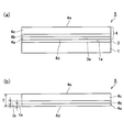
- (A) is a schematic diagram showing a state in which a seed crystal film 3 is formed on a single crystal substrate 1, and (b) shows a state in which a first void deficient layer 4 a is provided on the seed crystal film 3. It is a schematic diagram, (c) is a schematic diagram showing a state in which a void distribution layer 4b is provided on the first void-deficient layer.
- (A) is a schematic diagram which shows the state which provided the 2nd void deficient layer 4c on the void distribution layer,
- (b) is a schematic diagram which shows the self-supporting substrate 6 which consists of a group 13 element nitride layer.
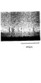
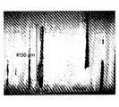
- . 3 shows a temperature profile that can be used to produce a Group 13 element nitride layer of the present invention. It is a microscope picture of the group 13 element nitride layer obtained in this invention Example. The partial enlarged photograph of FIG. 4 is shown.
- a seed crystal film 3 is formed on the growth surface 1 a of the single crystal substrate 1.
- a first void deficient layer 4 a is formed on the growth surface 3 a of the seed crystal film 3.
- a void distribution layer 4b is formed on the first void-deficient layer 4a.
- a second void-deficient layer 4c is formed on the void distribution layer 4b to obtain a group 13 element nitride layer 4.
- the composite substrate 5 is formed, and the functional element structure can be formed on the composite substrate 5.
- the group 13 element nitride layer 5 can be peeled from the seed crystal substrate to obtain a freestanding substrate 6 made of a group 13 element nitride layer.
- a functional element structure can be formed on the surface of the second void-deficient layer 4c.
- the group 13 element nitride layer 4 of the present invention has a first main surface 4d and a second main surface 4e.
- the first void deficient layer 4a provided on the first main surface 4d side
- the second void deficient layer 4c provided on the second main surface 4e side
- the void distribution layer 4b is provided between the layer 4c and the depletion layer 4c.
- the seed crystal substrate may include a single crystal substrate and a seed crystal film thereon, or may be a free-standing substrate made of a seed crystal.
- the material of the single crystal substrate is not limited, but sapphire, AlN template, GaN template, GaN free-standing substrate, silicon single crystal, SiC single crystal, MgO single crystal, spinel (MgAl 2 O 4 ), LiAlO 2 , LiGaO 2 , LaAlO 3 , LaGaO 3 , NdGaO 3 and other perovskite complex oxides, SCAM (ScAlMgO 4 ).
- cubic perovskite structure composite oxides (1) and (2) can be used.
- the material constituting the seed crystal is preferably a group 13 element nitride, and boron nitride (BN), aluminum nitride (AlN), gallium nitride (GaN), indium nitride (InN), thallium nitride (TlN), and mixed crystals thereof ( AlGaN: AlGaInN etc.).
- BN boron nitride
- AlN aluminum nitride
- GaN gallium nitride
- InN indium nitride
- TlN thallium nitride
- the seed crystal film is preferably formed by vapor deposition, but metal organic chemical vapor deposition (MOCVD), metal chemistry, chemical vapor deposition, hydride vapor deposition (HVPE), pulsed excitation deposition (PXD), MBE. Method and sublimation method. Metalorganic chemical vapor deposition is particularly preferred.
- Group 13 elements are Group 13 elements according to the periodic table established by IUPAC.
- the group 13 element is specifically gallium, aluminum, indium, thallium, or the like.
- the additive include carbon, low melting point metals (tin, bismuth, silver, gold) and high melting point metals (transition metals such as iron, manganese, titanium, and chromium).
- the low melting point metal may be added for the purpose of preventing oxidation of sodium, and the high melting point metal may be mixed from a container in which a crucible is put or a heater of a growth furnace.
- the group 13 element nitride is gallium nitride, aluminum nitride, or aluminum gallium nitride.
- voids are distributed in the group 13 element nitride.
- a void is a void free from nitrides and other inclusion components in a group 13 element nitride layer.
- the void in this specification is measured as follows.
- the seed crystal and the nitride film thereon are cut out along the cross section, and the cross section is polished with a diamond slurry having a particle size of about 1 micron. Then, a cross section is photographed with a transmission optical microscope having a magnification of 200 times. Then, the number of voids having a diameter of 1 ⁇ m or more in each layer is counted for a length of 100 ⁇ m along the interface between the single crystal and the group 13 element nitride layer.
- the average diameter of voids in each layer is preferably 1.5 to 6 ⁇ m.
- the diameter of each void is calculated as follows. That is, as described above, after taking a cross section of the group 13 element nitride crystal layer with a transmission optical microscope of 200 times magnification, in this cross section photograph, each void is perpendicular to the growth direction of each layer. The length in the direction is measured, and the maximum value of the measured values for each void is taken as the diameter.
- the number of voids having a diameter of 1 ⁇ m or more per 100 ⁇ m length in each void-deficient layer is preferably 1 or less from the viewpoint of film quality, and it is desirable that voids having a diameter of 1 ⁇ m or more are not observed.
- the number of voids having a diameter of 1 ⁇ m or more per 100 ⁇ m length in the void distribution layer is preferably 3 or more, more preferably 5 or more from the viewpoint of relaxing stress and preventing cracks. . Further, from the viewpoint of film quality, 15 or less is preferable, and 10 or less is more preferable.
- the thickness ta (see FIG. 2B) of the first void-deficient layer 4a is 30 ⁇ m or more. This makes it easier to relieve stress in the void distribution layer 4b. From this point of view, the thickness ta of the first void-deficient layer 4a is more preferably 50 ⁇ m or more. Further, from the viewpoint of film quality, the thickness ta of the first void-deficient layer 4a is preferably 150 ⁇ m or less, and more preferably 100 ⁇ m or less.
- the functional element of the present invention includes the group 13 element nitride layer and a functional layer provided on the second main surface.
- the functional element of the present invention is used in a technical field that is required to have high quality, for example, a high color rendering white LED called a post-fluorescent lamp, a blue-violet laser for high-speed and high-density optical memory, a pure blue, and a pure green light source. It can be used for power devices used in LEDs, lasers, inverters for hybrid vehicles, and the like.
- the production method of the group 13 element nitride layer of the present invention is not particularly limited, and is a liquid phase method such as a flux method, a metal organic chemical vapor deposition (MOCVD) method, a hydride vapor phase epitaxy (HVPE). Examples thereof include gas phase methods such as the method, pulse excitation deposition (PXD) method, MBE method, and sublimation method.
- a liquid phase method such as a flux method, a metal organic chemical vapor deposition (MOCVD) method, a hydride vapor phase epitaxy (HVPE).
- gas phase methods such as the method, pulse excitation deposition (PXD) method, MBE method, and sublimation method.
- the temperature schedule is changed by at least three stages when the flux method is performed. Specifically, the film formation temperature Tb in the step (b) is lower than the film formation temperature Ta in the process (a), and the temperature is rapidly lowered. Then, the process (c) is lower than the film formation temperature Tb in the process (b). The film forming temperature Tc is increased.
- Such a temperature schedule is advantageous because when the film formation temperature is increased, the film formation rate is reduced and voids are less likely to occur, and when the film formation temperature is decreased, the film formation rate is increased and voids are likely to occur.
- the supersaturation degree in a flux changes abruptly, so that the temperature fall rate from Ta to Tb is quick, it becomes easy to produce a void and it is advantageous.
- film formation temperatures Ta, Tb, and Tc vary depending on the group 13 element nitride to be formed, but generally the following ranges are preferable.
- Ta and Tc 850 to 900 ° C. (preferably 860 to 880 ° C.)
- Tb 800 to 850 ° C. (preferably 820 to 850 ° C.)
- Ta-Tb and Tc-Tb 10 to 50 ° C. (preferably 20 to 40 ° C.)
- the rate of temperature decrease from Ta to Tb is preferably 12 to 90 ° C./hour, and the rate of temperature increase from Tb to Tc is preferably 50 to 500 ° C./min.
- the pressure during film formation is preferably 3.0 to 5.0 MPa, more preferably 3.3 to 4.5 MPa.
- void control can be performed by relatively reducing the pressures PA and PC in the steps (a) and (c) and relatively increasing the pressure PB in the step (b).
- PB-PA and PB-PC are preferably set to 0.2 MPa or more.
- the ease of generating voids can be controlled by rotating the container containing the melt.
- the rotational speeds Ra and Rc of the container are preferably 10 to 50 rpm.
- the rotational speed Rb of the container is preferably 10 to 100 rpm.
- the rotation stop time is preferably 1 second to 6000 seconds, more preferably 10 seconds to 3600 seconds.
- the rotation time before and after the rotation stop time is preferably 10 seconds to 3600 seconds.
- the ratio of the group 13 element nitride / flux (for example, sodium) in the melt (mole ratio is preferably increased from the viewpoint of the present invention, preferably 18 mol% or more, more preferably 25 mol% or more.
- the formation of voids can be promoted, but if this ratio becomes too large, the crystal quality tends to deteriorate, so 40 mol% or less is preferable.
- Example 1 A gallium nitride crystal layer was grown in accordance with the method described with reference to FIGS. Specifically, a 5 micron thick gallium nitride seed crystal film 3 is epitaxially grown by MOCVD on a c-plane sapphire substrate 1 having a diameter of 3 inches and a thickness of 0.25 mm to produce a so-called GaN template (FIG. 1 ( a)).
- a gallium nitride single crystal layer 4 was grown on the seed crystal film 3 by a flux method. Specifically, a cylindrical flat bottom crucible having an inner diameter of 80 mm and a height of 45 mm was used, and the raw materials for growth (metal Ga 60 g, metal Na 60 g) were melted in a glove box and filled in the crucible. First, Na was filled, and then Ga was filled to shield Na from the atmosphere and prevent oxidation. The melt height of the raw material in the crucible was about 15 mm.
- the crucible was put in a refractory metal container and hermetically sealed, and then placed on a stage where the crystal growth furnace could be rotated.
- the temperature was raised to 870 ° C and 4.5 MPa, and then held for 5 hours. During this time, the solution was rotated to grow crystals while stirring (step (a)).
- the rotation conditions were as follows. Rotation speed: 10rpm Rotation time: 600 seconds Stop time: 600 seconds
- step (b) the temperature was decreased to 840 ° C. over 1 hour (temperature decrease rate: 30 ° C./hour), and held there for 3 hours (step (b)).
- step (c) the temperature was raised again to 870 ° C. (temperature raising rate 300 ° C./hour), and crystal growth was performed over 92 hours (step (c)). Thereafter, it was gradually cooled to room temperature over 10 hours.
- the grown crystal was grown to a thickness of 1.3 mm.
- the in-plane thickness variation was small, less than 10%.
- 4 and 5 show cross-sectional photographs of the obtained crystal. When observed from the cross-sectional direction, the first void-deficient layer, void distribution layer, and second void-deficient layer were seen from the sapphire substrate 1 side, and the structure was a three-layer structure.
- each layer is as follows.
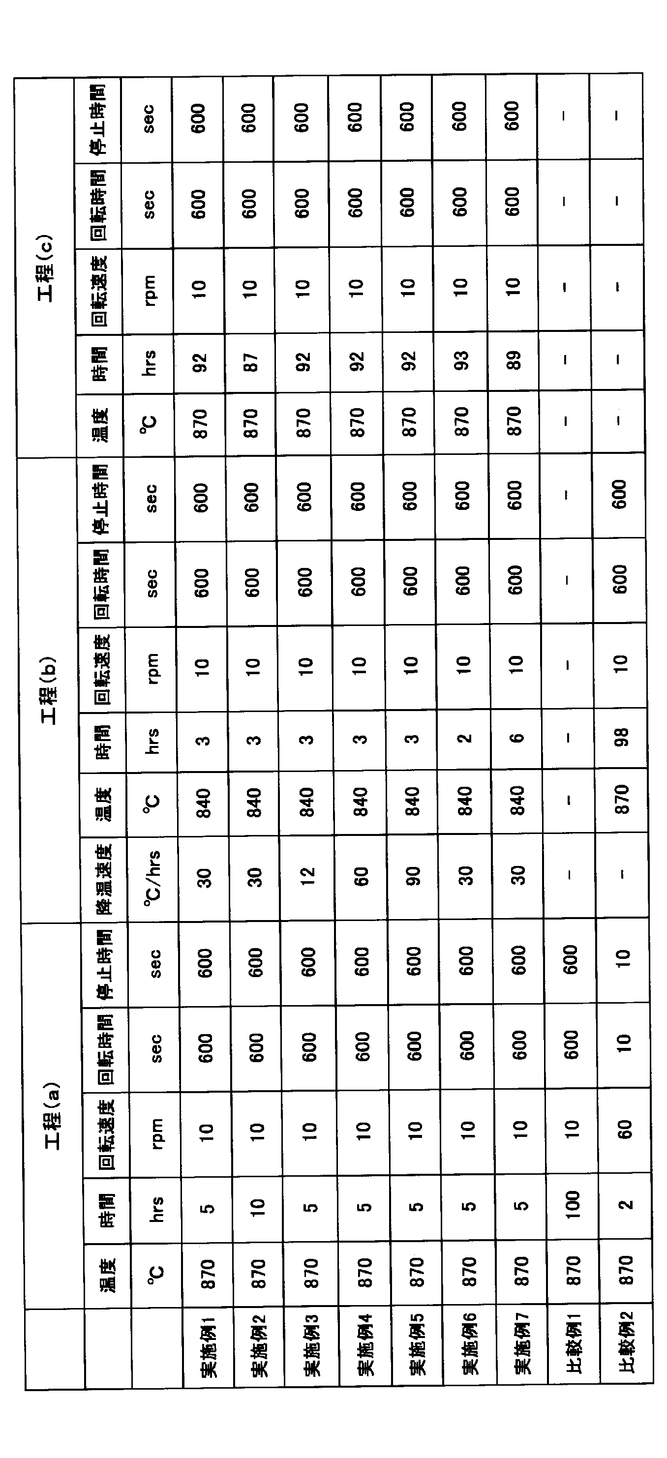
- Examples 2 to 7 The group 13 element nitride layer of each example was formed in the same manner as in Example 1. However, the conditions in steps (a), (b), and (c) were changed as shown in Table 1.
- Table 1 shows the structure of each of the obtained group 13 element nitride layers in each example. Moreover, about the obtained group 13 element nitride layer of each example, the presence or absence of the crack in a group 13 element nitride layer was observed after the growth and after peeling by the laser lift-off method. The results are shown in Table 2.
- Example 1 A gallium nitride crystal layer was grown in accordance with the method described with reference to FIGS. Specifically, the same GaN template as in Example 1 was produced (FIG. 1A).
- a gallium nitride single crystal layer was grown on the seed crystal film 3 by a flux method. Specifically, a cylindrical flat bottom crucible having an inner diameter of 80 mm and a height of 45 mm was used, and the raw materials for growth (metal Ga 60 g, metal Na 60 g) were melted in a glove box and filled in the crucible. First, Na was filled, and then Ga was filled to shield Na from the atmosphere and prevent oxidation. The melt height of the raw material in the crucible was about 15 mm.
- the crucible was put in a refractory metal container and hermetically sealed, and then placed on a stage where the crystal growth furnace could be rotated. After raising the temperature and pressing up to 870 ° C. and 4.5 MPa, it was maintained for 100 hours to grow crystals. During this period, the solution was rotated to grow crystals while stirring.
- the rotation conditions are as follows. Rotation speed: 10rpm Rotation time: 600 seconds Stop time: 600 seconds
- the grown crystal was grown to a thickness of 1.3 mm.
- the in-plane thickness variation was small, less than 10%.
- a cross-sectional photograph of the obtained crystal was observed, it was a single layer structure as viewed from the sapphire substrate 1 side.
- the structure of this layer is as follows. Thickness: 1.3mm Number of voids per 100 ⁇ m length: 0
- the crack generation rate was 40%.
- Each group 13 element nitride layer was separated from the sapphire substrate by a laser lift-off method. As a result of repeating the same experiment 10 times, the crack occurrence rate in the group 13 element nitride layer was 40%.
- Example 2 A gallium nitride crystal layer was grown in accordance with the method described with reference to FIGS. Specifically, the same GaN template as in Example 1 was produced (FIG. 1A).
- a gallium nitride single crystal layer 4 was grown on the seed crystal film 3 by a flux method. Specifically, a cylindrical flat bottom crucible having an inner diameter of 80 mm and a height of 45 mm was used, and the raw materials for growth (metal Ga 60 g, metal Na 60 g) were melted in a glove box and filled in the crucible. First, Na was filled, and then Ga was filled to shield Na from the atmosphere and prevent oxidation. The melt height of the raw material in the crucible was about 15 mm.
- the crucible was put in a refractory metal container and hermetically sealed, and then placed on a stage where the crystal growth furnace could be rotated.
- the temperature was increased to 870 ° C. and 4.5 MPa, and then held for 2 hours to grow crystals.
- the rotation conditions are as follows. Rotation speed: 60rpm Rotation time: 10 seconds Stop time: 10 seconds
- the grown crystal was grown to a thickness of 1.3 mm.
- the in-plane thickness variation was small and less than 10%.
- a cross-sectional photograph of the obtained crystal was observed, it was a two-layer structure as viewed from the sapphire substrate 1 side.
- the structure of each layer is as follows. Void distribution layer: Thickness: 20 ⁇ m Number of voids per 100 ⁇ m length: 10 void-deficient layers: Number of voids per 100 ⁇ m length: 0 Total thickness of group 13 element nitride layer: 1.3 mm
Landscapes
- Chemical & Material Sciences (AREA)
- Engineering & Computer Science (AREA)
- Crystallography & Structural Chemistry (AREA)
- Materials Engineering (AREA)
- Metallurgy (AREA)
- Organic Chemistry (AREA)
- Inorganic Chemistry (AREA)
- Crystals, And After-Treatments Of Crystals (AREA)
Abstract
第一の主面および第二の主面を有する13族元素窒化物層を提供する。13族元素窒化物層は、第一の主面側に設けられた第一のボイド欠乏層、第二の主面側に設けられた第二のボイド欠乏層、および第一の欠乏層と第二の欠乏層との間に設けられたボイド分布層を備えている。
Description
本発明は、13族元素窒化物層、複合基板および機能素子に関するものである。
窒化ガリウム単結晶からなる自立基板の作製方法として、サファイアやGaAsといった異種材料を下地基板とし、この上に厚膜の窒化ガリウム結晶を成長させ、その後、下地基板を除去する方法が知られている。この場合、下地基板と窒化ガリウムの熱膨張率が異なるため、冷却中に応力が発生するため、下地基板と窒化ガリウム結晶からなる複合基板の反りが大きく、窒化ガリウム結晶や下地基板にクラックが発生しやすくなり、歩留りが低下する。また、複合基板の反りが大きいと、例えばレーザーリフトオフなどの方法で下地基板を除去する際にクラックが発生するといった問題がある。
特許文献1(特開2012-126602)によれば、種結晶基板の表面に空隙を作製し、この部分から結晶成長させることにより、種結晶基板と育成した結晶との接触面積を減らし、冷却時の熱膨張差を利用して、成長後の結晶を剥離させている。
一方、特許文献2(WO2013/021804 A2)によれば、種結晶膜の界面に沿って、インクルージョン(異相)の多いインクルージョン分布層を形成することで、レーザーリフトオフ法によってクラックなく窒化ガリウムを剥離可能であると記載している。
また、特許文献3、4(特開2009-91225、特開2009-91226)によれば、温度や圧力を制御することで、窒化ガリウム結晶の成長効率を高めることを提案している。
また、特許文献3、4(特開2009-91225、特開2009-91226)によれば、温度や圧力を制御することで、窒化ガリウム結晶の成長効率を高めることを提案している。
しかし、特許文献1の方法では、窒化ガリウム結晶の剥離の成功率に限界があり、クラック抑制が十分ではない。
特許文献2では、種結晶膜上にインクルージョン分布層を形成し、その上にインクルージョン欠乏層を形成することによって、転位欠陥をインクルージョン分布層で吸収し、クラックを抑制する。しかし、インクルージョン欠乏層の厚さやインクルージョンのサイズを制御することが難しく、インクルージョン欠乏層にクラックが発生することがあった。
特許文献3、4は、窒化ガリウム結晶の成長速度を高める技術であるが、クラック抑制等については記載がない。
本発明の課題は、13族元素窒化物層のクラックを抑制できるような層構造を提供することである。
本発明は、第一の主面および第二の主面を有する13族元素窒化物層であって、
前記第一の主面側に設けられた第一のボイド欠乏層、
前記第二の主面側に設けられた第二のボイド欠乏層、および
前記第一の欠乏層と前記第二の欠乏層との間に設けられたボイド分布層
を備えていることを特徴とする、13族元素窒化物層に係るものである。
前記第一の主面側に設けられた第一のボイド欠乏層、
前記第二の主面側に設けられた第二のボイド欠乏層、および
前記第一の欠乏層と前記第二の欠乏層との間に設けられたボイド分布層
を備えていることを特徴とする、13族元素窒化物層に係るものである。
また、本発明は、
種結晶基板、および
前記種結晶基板の表面に設けられた、前記13族元素窒化物層を備えていることを特徴とする、複合基板に係るものである。
種結晶基板、および
前記種結晶基板の表面に設けられた、前記13族元素窒化物層を備えていることを特徴とする、複合基板に係るものである。
また、本発明は、前記13族元素窒化物層、および
前記13族元素窒化物層の第二の主面上に設けられた機能層を備えていることを特徴とする、機能素子に係るものである。
前記13族元素窒化物層の第二の主面上に設けられた機能層を備えていることを特徴とする、機能素子に係るものである。
本発明者は、種結晶上に13族元素窒化物層を形成するのに際して、まずボイドの乏しい第一のボイド欠乏層を形成し、その上にボイドの多いボイド分布層を形成した上で、ボイド分布層上にふたたび第二のボイド欠乏層を形成し、三層構造を提供することを想到した。すなわち、ボイド分布層と種結晶膜界面との間に第一のボイド欠乏層を配置する構造を製造することに成功した。
その上で、得られた13族元素窒化物層を精査したところ、第二のボイド欠乏層におけるクラックが著しく低減されることを見いだし、本発明に到達した。
この理由は明らかではない。しかし、13族元素窒化物層を冷却したときに、応力が、13族元素窒化物層と種結晶表面との界面には集中せず、この界面から13族元素窒化物層内に向かってある程度離れた場所に集中することが判明した。このため、ボイド分布層を、前記界面から13族元素窒化物層中に離れた場所に設けることによって、冷却時の応力をボイド分布層あるいはその近辺に集中させ、応力を緩和させることができ、またはボイド分布層によってクラックの進展を抑制することができ、その上の第二のボイド欠乏層内でのクラックを抑制できたものと考えられる。
以下、図面を適宜参照しつつ、本発明の実施形態を更に説明する。
図1(a)に示すように、単結晶基板1の育成面1a上に種結晶膜3を形成する。次いで、図1(b)に示すように、種結晶膜3の育成面3a上に、第一のボイド欠乏層4aを形成する。次いで、図1(c)に示すように、第一のボイド欠乏層4a上にボイド分布層4bを形成する。次いで、図2(a)に示すように、ボイド分布層4b上に、第二のボイド欠乏層4cを成膜し、13族元素窒化物層4を得る。
図1(a)に示すように、単結晶基板1の育成面1a上に種結晶膜3を形成する。次いで、図1(b)に示すように、種結晶膜3の育成面3a上に、第一のボイド欠乏層4aを形成する。次いで、図1(c)に示すように、第一のボイド欠乏層4a上にボイド分布層4bを形成する。次いで、図2(a)に示すように、ボイド分布層4b上に、第二のボイド欠乏層4cを成膜し、13族元素窒化物層4を得る。
図2(a)の状態で、複合基板5とし、複合基板5上に機能素子構造を成膜することができる。あるいは、図2(b)に示すように、13族元素窒化物層5を種結晶基板から剥離させ、13族元素窒化物層からなる自立基板6を得ることができる。この場合には、第二のボイド欠乏層4cの表面上に機能素子構造を成膜できる。
本発明の13族元素窒化物層4は、第一の主面4dおよび第二の主面4eを有する。そして、第一の主面4d側に設けられた第一のボイド欠乏層4a、第二の主面4e側に設けられた第二のボイド欠乏層4c、および第一の欠乏層4aと第二の欠乏層4cとの間に設けられたボイド分布層4bを有する。
以下、本発明の各構成要素について更に説明する。
(種結晶基板)
種結晶基板は、単結晶基板およびその上の種結晶膜を備えていてよく、あるいは、種結晶からなる自立基板であってよい。
(種結晶基板)
種結晶基板は、単結晶基板およびその上の種結晶膜を備えていてよく、あるいは、種結晶からなる自立基板であってよい。
単結晶基板の材質は限定されないが、サファイア、AlNテンプレート、GaNテンプレート、GaN自立基板、シリコン単結晶、SiC単結晶、MgO単結晶、スピネル(MgAl2O4)、LiAlO2、LiGaO2、LaAlO3,LaGaO3,NdGaO3等のペロブスカイト型複合酸化物、SCAM(ScAlMgO4)を例示できる。また組成式〔A1-y(Sr1-xBax)y〕〔(Al1-zGaz)1-u・Du〕O3(Aは、希土類元素である;Dは、ニオブおよびタンタルからなる群より選ばれた一種以上の元素である;y=0.3~0.98;x=0~1;z=0~1;u=0.15~0.49;x+z=0.1~2)の立方晶系のペロブスカイト構造複合酸化物も使用できる。
種結晶を構成する材質は13族元素窒化物が好ましく、窒化ホウ素(BN)、窒化アルミニウム(AlN)、窒化ガリウム(GaN)、窒化インジウム(InN)、窒化タリウム(TlN)、これらの混晶(AlGaN:AlGaInN等)が挙げられる。
種結晶膜の形成方法は気相成長法が好ましいが、有機金属化学気相成長(MOCVD: Metal Organic Chemical Vapor Deposition)法、ハイドライド気相成長(HVPE)法、パルス励起堆積(PXD)法、MBE法、昇華法を例示できる。有機金属化学気相成長法が特に好ましい。
(13族元素窒化物層)
13族元素とは、IUPACが策定した周期律表による第13族元素のことである。13族元素は、具体的にはガリウム、アルミニウム、インジウム、タリウム等である。また、添加剤としては、炭素や、低融点金属(錫、ビスマス、銀、金)、高融点金属(鉄、マンガン、チタン、クロムなどの遷移金属)が挙げられる。低融点金属は、ナトリウムの酸化防止を目的として添加する場合があり、高融点金属は、坩堝を入れる容器や育成炉のヒーターなどから混入する場合がある。
13族元素とは、IUPACが策定した周期律表による第13族元素のことである。13族元素は、具体的にはガリウム、アルミニウム、インジウム、タリウム等である。また、添加剤としては、炭素や、低融点金属(錫、ビスマス、銀、金)、高融点金属(鉄、マンガン、チタン、クロムなどの遷移金属)が挙げられる。低融点金属は、ナトリウムの酸化防止を目的として添加する場合があり、高融点金属は、坩堝を入れる容器や育成炉のヒーターなどから混入する場合がある。
好適な実施形態においては、13族元素窒化物が窒化ガリウム、窒化アルミニウムまたは窒化アルミニウムガリウムであ。
ボイド分布層においては、ボイドが13族元素窒化物中に分布している。ボイドは、13族元素窒化物層中で、窒化物やその他の包含成分がない空隙のことである。本明細書におけるボイドとは、以下のようにして測定されるものである。
すなわち、種結晶およびその上の窒化物膜を横断面に沿って切り出し、横断面を粒径1ミクロン程度のダイヤモンドスラリーで研磨する。そして倍率200倍の透過型光学顕微鏡で横断面を撮影する。その上で、単結晶と13族元素窒化物層との界面に沿って長さ100μmについて、各層において、径1μm以上のボイドの数を計数する。
各層におけるボイドの平均径は、1.5~6μmであることが好ましい。ここで、各ボイドの径は、以下のようにして算出する。
すなわち、上述したように、倍率200倍の透過型光学顕微鏡で13族元素窒化物結晶層の横断面を撮影した後、この横断面写真において、各ボイドについて、各層の成長方向に対して垂直な方向の長さを測定し、各ボイドについてこの測定値の最大値を径とする。
すなわち、上述したように、倍率200倍の透過型光学顕微鏡で13族元素窒化物結晶層の横断面を撮影した後、この横断面写真において、各ボイドについて、各層の成長方向に対して垂直な方向の長さを測定し、各ボイドについてこの測定値の最大値を径とする。
好適な実施形態においては、各ボイド欠乏層における長さ100μmあたりの径1μm以上のボイド数は、膜品質の観点からは、1個以下が好ましく、径1μm以上のボイドが観察されないことが望ましい。
好適な実施形態においては、ボイド分布層における長さ100μmあたりの径1μm以上のボイド数は、応力を緩和してクラックを防止するという観点からは、3個以上が好ましく、5個以上が更に好ましい。また、膜品質の観点からは、15個以下が好ましく、 10個以下が更に好ましい。
好ましくは、第一のボイド欠乏層4aの厚さta(図2(b)参照)が30μm以上である。これによって、ボイド分布層4bで応力を緩和しやすくなる。この観点からは、第一のボイド欠乏層4aの厚さtaは50μm以上が更に好ましい。また、膜品質の観点からは、第一のボイド欠乏層4aの厚さtaは150μm以下が好ましく、100μm以下が更に好ましい。
(機能素子)
本発明の機能素子は、前記13族元素窒化物層、および
第二の主面上に設けられた機能層を備えている。
本発明の機能素子は、前記13族元素窒化物層、および
第二の主面上に設けられた機能層を備えている。
本発明の機能素子は、高品質であることが要求される技術分野、例えばポスト蛍光灯といわれている高演色性の白色LEDや高速高密度光メモリ用青紫レーザ、純青色、純緑色の光源用LEDやレーザ、ハイブリッド自動車用のインバータに用いるパワーデバイスなどに用いることができる。
(13族元素窒化物層の製法例)
本発明の13族元素窒化物層の製法は特に限定されず、フラックス法のような液相法、有機金属化学気相成長(MOCVD: Metal Organic Chemical Vapor Deposition)法、ハイドライド気相成長(HVPE)法、パルス励起堆積(PXD)法、MBE法、昇華法のような気相法を例示できる。
本発明の13族元素窒化物層の製法は特に限定されず、フラックス法のような液相法、有機金属化学気相成長(MOCVD: Metal Organic Chemical Vapor Deposition)法、ハイドライド気相成長(HVPE)法、パルス励起堆積(PXD)法、MBE法、昇華法のような気相法を例示できる。
具体的には、種結晶上に13族元素窒化物層を成膜するのに際して、各層のボイド数を増大し、あるいは減少させるような条件を選択する。
以下、フラックス法の例について説明する。
好適な実施形態においては、図3に示すように、フラックス法の実施に際して、温度スケジュールを少なくとも3段階変更する。具体的には、工程(a)における成膜温度Taよりも工程(b)における成膜温度Tbを低く、急速に降温し、次いで、工程(b)における成膜温度Tbよりも工程(c)における成膜温度Tcを高くする。成膜温度を上げると成膜速度が低くなり、ボイドが生じにくくなるし、成膜温度を下げると成膜速度が高くなり、ボイドが生じやすくなるので、こうした温度スケジュールは有利である。また、TaからTbへの降温速度が速いほど、フラックス中の過飽和度が急激に変化するため、ボイドが生じやすくなり、有利である。
好適な実施形態においては、図3に示すように、フラックス法の実施に際して、温度スケジュールを少なくとも3段階変更する。具体的には、工程(a)における成膜温度Taよりも工程(b)における成膜温度Tbを低く、急速に降温し、次いで、工程(b)における成膜温度Tbよりも工程(c)における成膜温度Tcを高くする。成膜温度を上げると成膜速度が低くなり、ボイドが生じにくくなるし、成膜温度を下げると成膜速度が高くなり、ボイドが生じやすくなるので、こうした温度スケジュールは有利である。また、TaからTbへの降温速度が速いほど、フラックス中の過飽和度が急激に変化するため、ボイドが生じやすくなり、有利である。
成膜温度Ta、Tb、Tcの具体的数値は、成膜するべき13族元素窒化物によって変化するが、一般的には以下の範囲が好ましい。
TaおよびTc: 850~900℃(好ましくは860~880℃)
Tb: 800~850℃(好ましくは820~850℃)
Ta-TbおよびTc-Tb: 10~50℃(好ましくは20~40℃)
Tb: 800~850℃(好ましくは820~850℃)
Ta-TbおよびTc-Tb: 10~50℃(好ましくは20~40℃)
また、TaからTbへの降温速度は、12~90℃/時間とすることが好ましく、TbからTcへの昇温速度は50~500℃/分とすることが好ましい。
また、成膜時の圧力については、3.0~5.0MPaとすることが好ましく、3.3~4.5MPaとすることが更に好ましい。また、工程(a)、工程(c)における圧力PA、PCを相対的に低くし、工程(b)における圧力PBを相対的に高くすることによって、ボイド制御できる。この観点からは、PB-PA、PB-PCは、0.2MPa以上とすることが好ましい。
また、融液を収容する容器を回転させることによって、ボイドの生成しやすさを制御することができる。例えば、工程(a)、工程(c)においては、容器の回転速度Ra、Rcを10~50rpmとすることが好ましい。また、工程(b)においては、容器の回転速度Rbを10~100rpmとすることが好ましい。
また、本発明の13族元素窒化物層を生成させる上で、容器の回転を停止させることが好ましい。この場合には、回転停止時間は1秒~6000秒が好ましく、10秒~3600秒が更に好ましい。また、回転停止時間の前後における回転時間は10秒~3600秒が好ましい。
融液における13族元素窒化物/フラックス(例えばナトリウム)の比率(mol比率は、本発明の観点からは、高くすることが好ましく、18mol%以上が好ましく、25mol%以上が更に好ましい。これを大きくすることで、ボイドの生成を促進できる。ただし、この割合が大きくなり過ぎると結晶品質が落ちる傾向があるので、40mol%以下が好ましい。
(実施例1)
図1~図3を参照しつつ説明した方法に従い、窒化ガリウム結晶層を育成した。
具体的には、直径3インチ、厚さ0.25mmのc面サファイア基板1に、厚さ5ミクロンの窒化ガリウム種結晶膜3をMOCVD法によりエピタキシャル成長させ、いわゆるGaNテンプレートを作製した(図1(a))。
図1~図3を参照しつつ説明した方法に従い、窒化ガリウム結晶層を育成した。
具体的には、直径3インチ、厚さ0.25mmのc面サファイア基板1に、厚さ5ミクロンの窒化ガリウム種結晶膜3をMOCVD法によりエピタキシャル成長させ、いわゆるGaNテンプレートを作製した(図1(a))。
次いで、フラックス法によって、種結晶膜3上に窒化ガリウム単結晶層4を育成した。
具体的には、内径80mm、高さ45mmの円筒平底坩堝を用い、育成原料(金属Ga60g、金属Na60g)をグローブボックス内でそれぞれ融解して坩堝内に充填した。まずNaを充填し、その後Gaを充填することにより、Naを雰囲気から遮蔽し、酸化を防止した。坩堝内の原料の融液高さは約15mmとなった。
具体的には、内径80mm、高さ45mmの円筒平底坩堝を用い、育成原料(金属Ga60g、金属Na60g)をグローブボックス内でそれぞれ融解して坩堝内に充填した。まずNaを充填し、その後Gaを充填することにより、Naを雰囲気から遮蔽し、酸化を防止した。坩堝内の原料の融液高さは約15mmとなった。
この坩堝を耐熱金属製の容器に入れて密閉した後、結晶育成炉の回転が可能な台上に設置した。870℃・4.5MPaまで昇温加圧後、5時間保持した。この間、溶液を回転することで撹拌しながら結晶成長させた(工程(a))。回転条件は以下のようにした。
回転速度:10rpm
回転時間:600秒
停止時間:600秒
回転速度:10rpm
回転時間:600秒
停止時間:600秒
次いで、1時間かけて840℃まで降温し(降温速度30℃/時間)、そこで3時間保持した(工程(b))。次いで、再び870℃まで昇温し(昇温速度300℃/時間)、92時間かけて結晶成長させた(工程(c))。その後10時間かけて室温まで徐冷した。
育成した結晶は、1.3mmの厚さで成長していた。面内の厚さバラツキは小さく、10%未満であった。得られた結晶の横断面写真を図4、図5に示す。横断面方向から観察すると、サファイア基板1側から観て、第一のボイド欠乏層、ボイド分布層、第二のボイド欠乏層が観られ、三層構造であった。
各層の構造は、以下のとおりである。
第一のボイド欠乏層:
厚さ: 65μm
長さ100μmあたりのボイド数: 0個
ボイド分布層:
厚さ: 50μm
長さ100μmあたりのボイド数: 5個
ボイド径(平均値): 2μm
第二のボイド欠乏層:
長さ100μmあたりのボイド数: 0個
13族元素窒化物層の合計厚さ: 1.3mm
第一のボイド欠乏層:
厚さ: 65μm
長さ100μmあたりのボイド数: 0個
ボイド分布層:
厚さ: 50μm
長さ100μmあたりのボイド数: 5個
ボイド径(平均値): 2μm
第二のボイド欠乏層:
長さ100μmあたりのボイド数: 0個
13族元素窒化物層の合計厚さ: 1.3mm
以上のような13族元素窒化物層を10体形成し、育成後のクラック発生数を調べたが、クラック発生率は0%であった。
また、各13族元素窒化物層について、レーザーリフトオフ法によってサファイア基板から分離した。同様の実験を10回繰り返した結果、13族元素窒化物層中のクラック発生率は0%であった。
また、各13族元素窒化物層について、レーザーリフトオフ法によってサファイア基板から分離した。同様の実験を10回繰り返した結果、13族元素窒化物層中のクラック発生率は0%であった。
(実施例2~7)
実施例1と同様にして各例の13族元素窒化物層を成膜した。
ただし、工程(a)、(b)、(c)における各条件を、表1に示すように変更した。
実施例1と同様にして各例の13族元素窒化物層を成膜した。
ただし、工程(a)、(b)、(c)における各条件を、表1に示すように変更した。
得られた各例の13族元素窒化物層について、各層の構造を表1に示す。また、得られた各例の13族元素窒化物層について、育成後およびレーザーリフトオフ法による剥離後について、13族元素窒化物層中のクラックの有無を観察した。結果を表2に示す。

(比較例1)
図1、図2を参照しつつ説明した方法に従い、窒化ガリウム結晶層を育成した。
具体的には、実施例1と同じGaNテンプレートを作製した(図1(a))。
図1、図2を参照しつつ説明した方法に従い、窒化ガリウム結晶層を育成した。
具体的には、実施例1と同じGaNテンプレートを作製した(図1(a))。
次いで、フラックス法によって、種結晶膜3上に窒化ガリウム単結晶層を育成した。
具体的には、内径80mm、高さ45mmの円筒平底坩堝を用い、育成原料(金属Ga60g、金属Na60g)をグローブボックス内でそれぞれ融解して坩堝内に充填した。まずNaを充填し、その後Gaを充填することにより、Naを雰囲気から遮蔽し、酸化を防止した。坩堝内の原料の融液高さは約15mmとなった。
具体的には、内径80mm、高さ45mmの円筒平底坩堝を用い、育成原料(金属Ga60g、金属Na60g)をグローブボックス内でそれぞれ融解して坩堝内に充填した。まずNaを充填し、その後Gaを充填することにより、Naを雰囲気から遮蔽し、酸化を防止した。坩堝内の原料の融液高さは約15mmとなった。
この坩堝を耐熱金属製の容器に入れて密閉した後、結晶育成炉の回転が可能な台上に設置した。870℃・4.5MPaまで昇温加圧後、100時間保持し、結晶を育成した。この間、溶液を回転することで撹拌しながら結晶成長させた。回転条件は以下のとおりである。
回転速度:10rpm
回転時間:600秒
停止時間:600秒
回転速度:10rpm
回転時間:600秒
停止時間:600秒
育成した結晶は、1.3mmの厚さで成長していた。面内の厚さバラツキは小さく、10%未満であった。得られた結晶の横断面写真を観察すると、サファイア基板1側から観て、一層構造であった。この層の構造は、以下のとおりである。
厚さ: 1.3mm
長さ100μmあたりのボイド数: 0個
厚さ: 1.3mm
長さ100μmあたりのボイド数: 0個
以上のような13族元素窒化物層を10体形成し、育成後のクラック発生数を調べたが、クラック発生率は40%であった。
また、各13族元素窒化物層について、レーザーリフトオフ法によってサファイア基板から分離した。同様の実験を10回繰り返した結果、13族元素窒化物層中のクラック発生率は40%であった。
また、各13族元素窒化物層について、レーザーリフトオフ法によってサファイア基板から分離した。同様の実験を10回繰り返した結果、13族元素窒化物層中のクラック発生率は40%であった。
(比較例2)
図1、図2を参照しつつ説明した方法に従い、窒化ガリウム結晶層を育成した。
具体的には、実施例1と同じGaNテンプレートを作製した(図1(a)。
図1、図2を参照しつつ説明した方法に従い、窒化ガリウム結晶層を育成した。
具体的には、実施例1と同じGaNテンプレートを作製した(図1(a)。
次いで、フラックス法によって、種結晶膜3上に窒化ガリウム単結晶層4を育成した。
具体的には、内径80mm、高さ45mmの円筒平底坩堝を用い、育成原料(金属Ga60g、金属Na60g)をグローブボックス内でそれぞれ融解して坩堝内に充填した。まずNaを充填し、その後Gaを充填することにより、Naを雰囲気から遮蔽し、酸化を防止した。坩堝内の原料の融液高さは約15mmとなった。
具体的には、内径80mm、高さ45mmの円筒平底坩堝を用い、育成原料(金属Ga60g、金属Na60g)をグローブボックス内でそれぞれ融解して坩堝内に充填した。まずNaを充填し、その後Gaを充填することにより、Naを雰囲気から遮蔽し、酸化を防止した。坩堝内の原料の融液高さは約15mmとなった。
この坩堝を耐熱金属製の容器に入れて密閉した後、結晶育成炉の回転が可能な台上に設置した。870℃・4.5MPaまで昇温加圧後、2時間保持し、結晶を育成した。回転条件は以下のとおりである。
回転速度:60rpm
回転時間:10秒
停止時間:10秒
回転速度:60rpm
回転時間:10秒
停止時間:10秒
次いで、870℃・4.5MPaのまま回転条件を以下のとおりに変更して98時間保持し、結晶を育成した。
回転速度:10rpm
回転時間:600秒
停止時間:600秒
回転速度:10rpm
回転時間:600秒
停止時間:600秒
育成した結晶は、1.3mmの厚さで成長していた。面内の厚さバラツキは小さく、10%未満であった。得られた結晶の横断面写真を観察すると、サファイア基板1側から観て、二層構造であった。
各層の構造は、以下のとおりである。
ボイド分布層:
厚さ:20μm
長さ100μmあたりのボイド数:10個
ボイド欠乏層:
長さ100μmあたりのボイド数: 0個
13族元素窒化物層の合計厚さ: 1.3mm
各層の構造は、以下のとおりである。
ボイド分布層:
厚さ:20μm
長さ100μmあたりのボイド数:10個
ボイド欠乏層:
長さ100μmあたりのボイド数: 0個
13族元素窒化物層の合計厚さ: 1.3mm
以上のような13族元素窒化物層を10体形成し、育成後のクラック発生数を調べたが、クラック発生率は20%であった。
また、各13族元素窒化物層について、レーザーリフトオフ法によってサファイア基板から分離した。同様の実験を10回繰り返した結果、13族元素窒化物層中のクラック発生率は30%であった。
また、各13族元素窒化物層について、レーザーリフトオフ法によってサファイア基板から分離した。同様の実験を10回繰り返した結果、13族元素窒化物層中のクラック発生率は30%であった。
Claims (10)
- 第一の主面および第二の主面を有する13族元素窒化物層であって、
前記第一の主面側に設けられた第一のボイド欠乏層、
前記第二の主面側に設けられた第二のボイド欠乏層、および
前記第一の欠乏層と前記第二の欠乏層との間に設けられたボイド分布層
を備えていることを特徴とする、13族元素窒化物層。 - 前記13族元素窒化物が窒化ガリウム、窒化アルミニウムまたは窒化アルミニウムガリウムであることを特徴とする、請求項1記載の13族元素窒化物層。
- 前記第一のボイド欠乏層の厚さが30~100μmであることを特徴とする、請求項1または2記載の13族元素窒化物層。
- 前記第一のボイド欠乏層および前記第二のボイド欠乏層の長さ100μm当たりのボイド数が1個以下であり、前記ボイド分布層の長さ100μm当たりのボイド数が3~10個であることを特徴とする、請求項1~3のいずれか一つの請求項に記載の13族元素窒化物層。
- 種結晶基板、および
前記種結晶基板の表面に設けられた、請求項1~4のいずれか一つの請求項に記載の13族元素窒化物層
を備えていることを特徴とする、複合基板。 - 前記種結晶基板が、単結晶基板、およびこの単結晶基板上に設けられた種結晶膜を備えており、前記種結晶膜が前記第一の主面に接していることを特徴とする、請求項5記載の複合基板。
- 請求項1~4のいずれか一つの請求項に記載の13族元素窒化物層、および
前記第二の主面上に設けられた機能層を備えていることを特徴とする、機能素子。 - 前記機能層が発光機能を有することを特徴とする、請求項7記載の機能素子。
- 更に種結晶基板を備えており、前記種結晶基板上に前記13族元素窒化物層が設けられていることを特徴とする、請求項7または8記載の機能素子。
- 前記種結晶基板が、単結晶基板、およびこの単結晶基板上に設けられた種結晶膜を備えており、前記種結晶膜が前記第一の主面に接していることを特徴とする、請求項9記載の機能素子。
Priority Applications (3)
| Application Number | Priority Date | Filing Date | Title |
|---|---|---|---|
| JP2018547504A JP6986024B2 (ja) | 2016-10-28 | 2017-09-29 | 複合基板および機能素子 |
| CN201780062316.5A CN109863262A (zh) | 2016-10-28 | 2017-09-29 | 13族元素氮化物层、复合基板以及功能元件 |
| US16/385,380 US11035055B2 (en) | 2016-10-28 | 2019-04-16 | Group 13 nitride layer, composite substrate, and functional element |
Applications Claiming Priority (2)
| Application Number | Priority Date | Filing Date | Title |
|---|---|---|---|
| JP2016-211564 | 2016-10-28 | ||
| JP2016211564 | 2016-10-28 |
Related Child Applications (1)
| Application Number | Title | Priority Date | Filing Date |
|---|---|---|---|
| US16/385,380 Continuation US11035055B2 (en) | 2016-10-28 | 2019-04-16 | Group 13 nitride layer, composite substrate, and functional element |
Publications (1)
| Publication Number | Publication Date |
|---|---|
| WO2018079192A1 true WO2018079192A1 (ja) | 2018-05-03 |
Family
ID=62024801
Family Applications (1)
| Application Number | Title | Priority Date | Filing Date |
|---|---|---|---|
| PCT/JP2017/035537 Ceased WO2018079192A1 (ja) | 2016-10-28 | 2017-09-29 | 13族元素窒化物層、複合基板および機能素子 |
Country Status (4)
| Country | Link |
|---|---|
| US (1) | US11035055B2 (ja) |
| JP (1) | JP6986024B2 (ja) |
| CN (1) | CN109863262A (ja) |
| WO (1) | WO2018079192A1 (ja) |
Families Citing this family (1)
| Publication number | Priority date | Publication date | Assignee | Title |
|---|---|---|---|---|
| WO2021100242A1 (ja) | 2019-11-21 | 2021-05-27 | 日本碍子株式会社 | 13族元素窒化物結晶層、自立基板および機能素子 |
Citations (3)
| Publication number | Priority date | Publication date | Assignee | Title |
|---|---|---|---|---|
| JP2007106666A (ja) * | 2005-10-12 | 2007-04-26 | Samsung Corning Co Ltd | フリースタンディング窒化ガリウム基板の製造方法 |
| JP2013249230A (ja) * | 2012-05-31 | 2013-12-12 | Mitsubishi Chemicals Corp | 周期表第13族金属窒化物半導体基板の製造方法 |
| JP2013252989A (ja) * | 2012-06-06 | 2013-12-19 | Mie Univ | 半導体素子用エピタキシャル基板、半導体素子用エピタキシャル基板の作製方法、およびAlN単結晶自立基板 |
Family Cites Families (7)
| Publication number | Priority date | Publication date | Assignee | Title |
|---|---|---|---|---|
| JP2004273661A (ja) * | 2003-03-07 | 2004-09-30 | Sumitomo Chem Co Ltd | 窒化ガリウム単結晶基板の製造方法 |
| JP4861953B2 (ja) | 2007-10-12 | 2012-01-25 | 日本碍子株式会社 | 窒化物単結晶の製造方法 |
| JP4861954B2 (ja) | 2007-10-12 | 2012-01-25 | 日本碍子株式会社 | 窒化物単結晶の製造方法 |
| JP5542040B2 (ja) | 2010-12-15 | 2014-07-09 | 日本碍子株式会社 | Iii族窒化物単結晶の製造方法およびこれに用いる種結晶基板 |
| JP5943921B2 (ja) | 2011-08-10 | 2016-07-05 | 日本碍子株式会社 | 13族元素窒化物膜の剥離方法 |
| JP6144630B2 (ja) * | 2012-08-30 | 2017-06-07 | 日本碍子株式会社 | 複合基板の製造方法、13族元素窒化物からなる機能層の製造方法 |
| JP5896470B2 (ja) * | 2012-11-16 | 2016-03-30 | 国立大学法人名古屋大学 | AlN単結晶の製造方法 |
-
2017
- 2017-09-29 CN CN201780062316.5A patent/CN109863262A/zh active Pending
- 2017-09-29 WO PCT/JP2017/035537 patent/WO2018079192A1/ja not_active Ceased
- 2017-09-29 JP JP2018547504A patent/JP6986024B2/ja not_active Expired - Fee Related
-
2019
- 2019-04-16 US US16/385,380 patent/US11035055B2/en not_active Expired - Fee Related
Patent Citations (3)
| Publication number | Priority date | Publication date | Assignee | Title |
|---|---|---|---|---|
| JP2007106666A (ja) * | 2005-10-12 | 2007-04-26 | Samsung Corning Co Ltd | フリースタンディング窒化ガリウム基板の製造方法 |
| JP2013249230A (ja) * | 2012-05-31 | 2013-12-12 | Mitsubishi Chemicals Corp | 周期表第13族金属窒化物半導体基板の製造方法 |
| JP2013252989A (ja) * | 2012-06-06 | 2013-12-19 | Mie Univ | 半導体素子用エピタキシャル基板、半導体素子用エピタキシャル基板の作製方法、およびAlN単結晶自立基板 |
Non-Patent Citations (1)
| Title |
|---|
| FUJITA, KOHEI ET AL.: "HVPE growth of thick A1N on trench-patterned substrate", PHYS. STATUS SOLIDI C, vol. 8, no. 5, 2011, pages 1483 - 1486 * |
Also Published As
| Publication number | Publication date |
|---|---|
| JPWO2018079192A1 (ja) | 2019-09-12 |
| US20190242029A1 (en) | 2019-08-08 |
| US11035055B2 (en) | 2021-06-15 |
| JP6986024B2 (ja) | 2021-12-22 |
| CN109863262A (zh) | 2019-06-07 |
Similar Documents
| Publication | Publication Date | Title |
|---|---|---|
| KR101936967B1 (ko) | 13족 원소 질화물막 및 그 적층체 | |
| JP5256198B2 (ja) | Iii族窒化物単結晶の製造方法 | |
| US9045844B2 (en) | Method for peeling group 13 element nitride film | |
| JP6344987B2 (ja) | 13族元素窒化物結晶層および機能素子 | |
| US20140158978A1 (en) | Semiconductor Light-Emitting Element and Laminate Containing Same | |
| JP5981074B1 (ja) | 13族元素窒化物結晶基板および機能素子 | |
| JP5426178B2 (ja) | Iii族金属窒化物単結晶の製造方法 | |
| JP6169292B1 (ja) | 13族元素窒化物結晶基板および機能素子 | |
| JP6986024B2 (ja) | 複合基板および機能素子 | |
| WO2016093033A1 (ja) | 13族元素窒化物結晶層および機能素子 | |
| JP4876002B2 (ja) | 窒化ガリウム単結晶育成用融液組成物および窒化ガリウム単結晶を育成する方法 | |
| JP6211087B2 (ja) | 13族元素窒化物の製造方法および融液組成物の製造方法 | |
| JP7491942B2 (ja) | 13族元素窒化物結晶層、自立基板および機能素子 | |
| JP5924800B1 (ja) | 13族元素窒化物結晶層および機能素子 | |
| JP2007254206A (ja) | 窒化物単結晶の育成方法 |
Legal Events
| Date | Code | Title | Description |
|---|---|---|---|
| 121 | Ep: the epo has been informed by wipo that ep was designated in this application |
Ref document number: 17863540 Country of ref document: EP Kind code of ref document: A1 |
|
| ENP | Entry into the national phase |
Ref document number: 2018547504 Country of ref document: JP Kind code of ref document: A |
|
| NENP | Non-entry into the national phase |
Ref country code: DE |
|
| 122 | Ep: pct application non-entry in european phase |
Ref document number: 17863540 Country of ref document: EP Kind code of ref document: A1 |