WO2018055699A1 - 基板処理装置、半導体装置の製造方法およびプログラム - Google Patents
基板処理装置、半導体装置の製造方法およびプログラム Download PDFInfo
- Publication number
- WO2018055699A1 WO2018055699A1 PCT/JP2016/077856 JP2016077856W WO2018055699A1 WO 2018055699 A1 WO2018055699 A1 WO 2018055699A1 JP 2016077856 W JP2016077856 W JP 2016077856W WO 2018055699 A1 WO2018055699 A1 WO 2018055699A1
- Authority
- WO
- WIPO (PCT)
- Prior art keywords
- processing
- chamber
- substrate
- transfer
- substrates
- Prior art date
- Legal status (The legal status is an assumption and is not a legal conclusion. Google has not performed a legal analysis and makes no representation as to the accuracy of the status listed.)
- Ceased
Links
Images


Classifications
-
- H—ELECTRICITY
- H10—SEMICONDUCTOR DEVICES; ELECTRIC SOLID-STATE DEVICES NOT OTHERWISE PROVIDED FOR
- H10P—GENERIC PROCESSES OR APPARATUS FOR THE MANUFACTURE OR TREATMENT OF DEVICES COVERED BY CLASS H10
- H10P72/00—Handling or holding of wafers, substrates or devices during manufacture or treatment thereof
- H10P72/30—Handling or holding of wafers, substrates or devices during manufacture or treatment thereof for conveying, e.g. between different workstations
- H10P72/33—Handling or holding of wafers, substrates or devices during manufacture or treatment thereof for conveying, e.g. between different workstations into and out of processing chamber
-
- H—ELECTRICITY
- H10—SEMICONDUCTOR DEVICES; ELECTRIC SOLID-STATE DEVICES NOT OTHERWISE PROVIDED FOR
- H10P—GENERIC PROCESSES OR APPARATUS FOR THE MANUFACTURE OR TREATMENT OF DEVICES COVERED BY CLASS H10
- H10P72/00—Handling or holding of wafers, substrates or devices during manufacture or treatment thereof
- H10P72/06—Apparatus for monitoring, sorting, marking, testing or measuring
- H10P72/0606—Position monitoring, e.g. misposition detection or presence detection
-
- H—ELECTRICITY
- H10—SEMICONDUCTOR DEVICES; ELECTRIC SOLID-STATE DEVICES NOT OTHERWISE PROVIDED FOR
- H10P—GENERIC PROCESSES OR APPARATUS FOR THE MANUFACTURE OR TREATMENT OF DEVICES COVERED BY CLASS H10
- H10P72/00—Handling or holding of wafers, substrates or devices during manufacture or treatment thereof
- H10P72/30—Handling or holding of wafers, substrates or devices during manufacture or treatment thereof for conveying, e.g. between different workstations
-
- H—ELECTRICITY
- H10—SEMICONDUCTOR DEVICES; ELECTRIC SOLID-STATE DEVICES NOT OTHERWISE PROVIDED FOR
- H10P—GENERIC PROCESSES OR APPARATUS FOR THE MANUFACTURE OR TREATMENT OF DEVICES COVERED BY CLASS H10
- H10P72/00—Handling or holding of wafers, substrates or devices during manufacture or treatment thereof
- H10P72/30—Handling or holding of wafers, substrates or devices during manufacture or treatment thereof for conveying, e.g. between different workstations
- H10P72/34—Handling or holding of wafers, substrates or devices during manufacture or treatment thereof for conveying, e.g. between different workstations the wafers being stored in a carrier, involving loading and unloading
- H10P72/3406—Handling or holding of wafers, substrates or devices during manufacture or treatment thereof for conveying, e.g. between different workstations the wafers being stored in a carrier, involving loading and unloading involving removal of lid, door or cover
-
- H—ELECTRICITY
- H10—SEMICONDUCTOR DEVICES; ELECTRIC SOLID-STATE DEVICES NOT OTHERWISE PROVIDED FOR
- H10P—GENERIC PROCESSES OR APPARATUS FOR THE MANUFACTURE OR TREATMENT OF DEVICES COVERED BY CLASS H10
- H10P95/00—Generic processes or apparatus for manufacture or treatments not covered by the other groups of this subclass
Definitions
- the present invention relates to a substrate processing apparatus, a semiconductor device manufacturing method, and a program.
- a single-wafer processing apparatus that processes substrates one by one or a small number of sheets and a vertical processing apparatus that processes a plurality of substrates at once are used.
- a processing apparatus that connects a single wafer processing apparatus and a vertical processing apparatus via a transfer chamber and can continuously process a substrate has been proposed (for example, Patent Document 1).
- an object of the present invention is to provide a technique capable of performing continuous processing with a single wafer processing apparatus and a vertical processing apparatus without complicating the apparatus configuration. It is to provide.
- a technique is provided that includes a transfer chamber that is adjacent to the first transfer chamber and the second transfer chamber and in which a transfer machine for transferring the substrate is installed.
- continuous processing can be performed by the single wafer processing apparatus and the vertical processing apparatus without complicating the apparatus configuration.
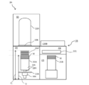
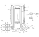
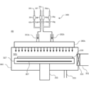
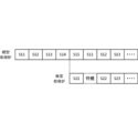
- Cross-sectional view of a substrate processing apparatus according to the present invention Front longitudinal section of substrate processing apparatus according to the present invention Vertical section around the vertical processing furnace according to the present invention Side surface longitudinal section of substrate processing apparatus according to the present invention Longitudinal sectional view around a single wafer processing furnace according to the present invention Sequence diagram in a vertical processing furnace and a single wafer processing furnace according to the present invention
- the transfer chamber 8 side described later is a front side (front side), and the transfer chambers 6A and 6B described later are back sides (rear sides). Furthermore, let the side which faces the boundary line (adjacent surface) of processing modules 3A and 3B, which will be described later, be the inside, and the side away from the boundary line be the outside.
- the substrate processing apparatus is configured as a substrate processing apparatus (hereinafter referred to as a processing apparatus) 2 that performs a substrate processing process such as a heat treatment as one process of the manufacturing process in the semiconductor device (device) manufacturing method. Yes.
- a substrate processing apparatus hereinafter referred to as a processing apparatus 2 that performs a substrate processing process such as a heat treatment as one process of the manufacturing process in the semiconductor device (device) manufacturing method.
- the substrate processing apparatus 2 includes two adjacent processing modules (casings) 3A and 3B.
- the processing module 3A is a vertical processing module that processes a plurality of substrates at once, and the processing module 3B is a single wafer processing module that processes substrates one by one.
- the processing modules 3A and 3B are configured by processing furnaces 4A and 4B and transfer chambers 6A and 6B as preparation chambers, respectively. Transfer chambers 6A and 6B are disposed below the processing furnaces 4A and 4B, respectively.
- a transfer chamber 8 having a transfer machine 7 for transferring a wafer W as a substrate is disposed adjacent to the transfer chambers 6A and 6B.
- a storage chamber 9 for storing a pod (hoop) 5 as a storage container for storing a plurality of wafers W is arranged on the front side of the transfer chamber 8.
- An I / O port 22 is installed on the entire surface of the storage chamber 9, and the pod 5 is carried into and out of the processing apparatus 2 through the I / O port 22.
- Gate valves 90 ⁇ / b> A and 90 ⁇ / b> B as isolation parts are respectively installed on boundary walls (adjacent surfaces) between the transfer chambers 6 ⁇ / b> A and 6 ⁇ / b> B and the transfer chamber 8.
- Pressure detectors are installed in the transfer chamber 8 and the transfer chambers 6A and 6B, respectively, and the pressure in the transfer chamber 8 is set to be lower than the pressure in the transfer chambers 6A and 6B.
- oxygen concentration detectors are installed in the transfer chamber 8 and the transfer chambers 6A and 6B, respectively. The oxygen concentration in the transfer chamber 8A and the transfer chambers 6A and 6B is higher than the oxygen concentration in the atmosphere. Is also kept low.
- a clean unit 62C for supplying clean air into the transfer chamber 8 is installed on the ceiling of the transfer chamber 8, and for example, an inert gas is circulated in the transfer chamber 8 as clean air. It is configured. By circulating and purging the inside of the transfer chamber 8 with an inert gas, the inside of the transfer chamber 8 can be made a clean atmosphere. With such a configuration, it is possible to prevent particles and the like in the transfer chambers 6A and 6B from entering the transfer chamber 8, and to naturally move on the wafer W in the transfer chamber 8 and the transfer chambers 6A and 6B. Formation of an oxide film can be suppressed.
- the processing furnace 4A is a vertical processing furnace that processes a plurality of substrates at once. As shown in FIG. 3, the processing furnace 4A includes a cylindrical reaction tube 10A and a heater 12A as a heating means (heating mechanism) installed on the outer periphery of the reaction tube 10A.
- the reaction tube is made of, for example, quartz or SiC.
- a processing chamber 14A for processing the wafer W as a substrate is formed inside the reaction tube 10A.
- a temperature detector 16A as a temperature detector is installed in the reaction tube 10A. The temperature detector 16A is erected along the inner wall of the reaction tube 10A.
- the gas used for substrate processing is supplied into the processing chamber 14A by a gas supply mechanism 34A as a gas supply system.
- the gas supplied by the gas supply mechanism 34A is changed according to the type of film to be formed.
- the gas supply mechanism 34A includes a source gas supply unit, a reaction gas supply unit, and an inert gas supply unit.
- the raw material gas supply unit includes a gas supply pipe 36a.
- a gas flow controller (MFC) 38a which is a flow rate controller (flow rate control unit), and a valve 40a, which is an on-off valve, are provided in order from the upstream direction. It has been.
- the gas supply pipe 36 a is connected to a nozzle 44 a that penetrates the side wall of the manifold 18.
- the nozzle 44a is erected in the vertical direction in the reaction tube 10A, and has a plurality of supply holes that open toward the wafer W held by the boat 26A as a substrate holder.
- the source gas is supplied to the wafer W through the supply hole of the nozzle 44a.
- the reaction gas is supplied to the wafer W from the reaction gas supply unit through the supply pipe 36b, the MFC 38b, the valve 40b, and the nozzle 44b with the same configuration.
- an inert gas is supplied to the wafer W via supply pipes 36c and 36d, MFCs 38c and 38d, valves 40c and 40d, and nozzles 44a and 44b.
- a cylindrical manifold 18A is connected to the lower end opening of the reaction tube 10A via a seal member such as an O-ring to support the lower end of the reaction tube 10A.
- the lower end opening portion 10B of the manifold 18 is formed facing the ceiling portion of the transfer chamber 6A, and is opened and closed by a disc-shaped lid portion 22A.
- a sealing member such as an O-ring is installed on the upper surface of the lid portion 22A, whereby the inside of the reaction tube 10A and the outside air are hermetically sealed.
- a substrate holder (boat) 26A which will be described later, is placed on the lid portion 22A via a heat insulating portion 24A.
- An exhaust pipe 46A is attached to the manifold 18.
- the exhaust pipe 46A is provided with a pressure sensor 48A as a pressure detector (pressure detection unit) for detecting the pressure in the processing chamber 14A and an APC (Auto Pressure Controller) valve 50A as a pressure regulator (pressure adjustment unit).
- a vacuum pump 52A as an evacuation device is connected. With such a configuration, the pressure in the processing chamber 14A can be set to a processing pressure corresponding to the processing.
- An exhaust system A is mainly configured by the exhaust pipe 46A, the APC valve 50A, and the pressure sensor 48A. The exhaust system A is accommodated in an exhaust box (not shown).
- the processing chamber 14A accommodates therein a boat 26A as a substrate holder for supporting a plurality of, for example, 25 to 50 wafers W vertically in a shelf shape.
- the boat 26A is made of, for example, quartz or SiC.
- the boat 26A is supported above the heat insulating portion 24A by a rotating shaft 28A that penetrates the lid portion 22A and the heat insulating portion 24A.
- the rotation shaft 28A is connected to a rotation mechanism 30A installed below the lid portion 22A, and the rotation shaft 28A is configured to be rotatable in a state where the inside of the reaction tube 10A is hermetically sealed.
- the lid portion 22A is driven in the vertical direction by a boat elevator 32A as a lifting mechanism. Accordingly, the boat 26A and the lid portion 22A are integrally lifted from the home position, and the boat 26A is transported between the transport chamber 6A and the reaction tube 10A.
- the transfer of the wafer W to the boat 26A is performed when the boat 26A is at the home position in the transfer chamber 6A.
- the home position is a position when the boat elevator 32 is not driving the lid portion 22A.
- a clean unit 60A is installed on one side of the transfer chamber 6A (the outer side of the transfer chamber 6A, the side opposite to the side facing the transfer chamber 6B), and the transfer chamber 6A. Clean air (for example, inert gas) is circulated in the interior.
- the inert gas supplied into the transfer chamber 6A is exhausted from the transfer chamber 6A by the exhaust part 62A installed on the side surface (side surface facing the transfer chamber 6B) facing the clean unit 60A across the boat 26A.
- the pressure in the transfer chamber 6 ⁇ / b> A is set to be lower than the pressure in the transfer chamber 8.
- the oxygen concentration in the transfer chamber 6A is set to be lower than the oxygen concentration in the atmosphere.
- the height of the transfer chamber 6A is set so that the transfer chamber 6A can be applied to at least two types of boats having different holding numbers.
- the transfer chamber 6A is configured such that, for example, when a boat 26A that holds N (N ⁇ 2) wafers W is used, a boat 26A ′ that holds 2N wafers W, which is double, can also be used. ing.
- the height of the boat 26A holding N wafers W from the floor surface of the transfer chamber 6A to the upper end of the boat is T2.
- the height of the transfer chamber 6A is at least higher than T1.
- the transfer machine 7 is also set to a height that can be driven up and down so that it can be applied to at least two types of boats with different numbers of holdings. That is, it is configured to be able to drive from a height position where the wafer W is transferred to the lowermost stage of the boat 26A and the boat 26A ′ to a height position where the wafer W is transferred to the uppermost stage of the boat 26A ′. With such a configuration, even if the type of boat is changed, there is no need to change the transfer machine 7, and the cost can be reduced.
- Utilities 120A such as a gas supply mechanism 34A and an exhaust mechanism of the processing furnace 4A are installed on the back surface (the back side of the processing module 3A) of the transfer chamber 6A.
- the processing furnace 4B is composed of a single wafer processing furnace that processes substrates one by one.
- the processing furnace 4B includes a processing container 303 that forms a processing chamber 301, a shower head 303s that supplies gas into the processing chamber 301 in a shower shape, and a support base that supports the wafer W in a horizontal posture. 317, a rotating shaft 355 that supports the support base 317 from below, and a heater 307 provided on the support base 317.
- the gas used for substrate processing is supplied into the processing chamber 301 by a gas supply mechanism 34B as a gas supply system.
- the gas supplied by the gas supply mechanism 34B is changed according to the substrate processing.
- the gas supply mechanism 34B includes a source gas supply unit, a reaction gas supply unit, and an inert gas supply unit.
- the source gas supply unit includes a supply pipe 36e, an MFC 38e, and a valve 40e
- the reaction gas supply unit includes a supply pipe 36f, an MFC 38f, and a valve 40f.
- the inert gas supply unit includes supply pipes 36g and 36h, MFCs 38g and 38h, and valves 40g and 40h.
- a gas supply port 332a for supplying the above-described raw material gas and a gas supply port 332b for supplying the above-described reaction gas are connected to an inlet (gas introduction port) of the shower head 303s.
- the above-described reaction gas supply unit and inert gas supply unit are connected to the gas supply port 332a.
- the gas supply port 332b is connected to the source gas supply unit and the inert gas supply unit described above.
- a gas dispersion plate that supplies gas into the processing chamber 301 in a shower shape is provided at the outlet (gas outlet) of the shower head 303s.
- the processing vessel 303 is provided with an exhaust port 333 that exhausts the inside of the processing chamber 301.
- An exhaust part is connected to the exhaust port 333 similarly to the processing furnace 4A.
- a transfer port 331 for carrying the wafer W in and out of the processing chamber 301 is formed on the front side surface of the processing container 303.
- the transfer port 331 is opened and closed by a gate valve 335.
- the gate valve 335 is closed, the inside of the processing container 303 and the outside air are hermetically sealed.
- the loading / unloading port 331 is formed on the side facing the transfer chamber 8. With such a configuration, the wafer W can be carried into and out of the processing container 303 using the transfer machine 7.
- a clean unit 60B is installed in the transfer chamber 6B in the same configuration as the transfer chamber 6A, and is configured to circulate clean air in the transfer chamber 6B.
- the oxygen concentration in the transfer chamber 6B is set to be lower than the oxygen concentration in the atmosphere, as in the transfer chamber 6A. With such a configuration, it is not necessary to install an evacuation chamber or the like between the transfer chamber 6B and the processing container 303, and the apparatus can be simplified.
- Utilities such as the gas supply mechanism 34B and the exhaust mechanism of the processing furnace 4B are installed on the upper surface of the processing furnace 3B (upper part of the processing module 3B). With such a configuration, the back side of the processing furnace 4B can be widely secured as a maintenance area, and workability can be improved.
- a mounting table 26B which is a rack for temporarily holding and holding the wafer W (temporarily placing the wafer W), is installed.
- the mounting table 26B is formed of, for example, quartz or SiC, and is configured to vertically support N wafers W in a shelf shape.
- the lowermost storage position of the pedestal 26B and the lowermost storage position of the boat 26A are configured to have the same height position.
- the uppermost storage position of the mounting table 26B and the uppermost storage position of the boat 26A are configured to be at the same height position.
- the pitch between the wafers W of the mounting table 26B and the pitch between the wafers W of the boat 26 are configured to be the same. That is, preferably, the mounting table 26B is configured in the same shape as the boat 26A, and is configured to store N wafers W. With such a configuration, the wafer W can be smoothly transferred from the transfer chamber 6A to the transfer chamber 6B.
- the mounting table 26B is installed so that the center of the wafer W supported by the mounting table 26B and the center of the wafer W mounted in the processing furnace 4B are on the same straight line.
- the horizontal distance between the transfer machine 7 to the wafer W on the mounting table 26B and the transfer machine 7 to the wafer W in the processing furnace 4B can be made the same, so that the wafer W is transferred with the same stroke.
- the wafer W can be loaded and unloaded, and the wafer W can be transferred quickly.
- the height of the transfer chamber 6B is formed lower than the height of the transfer chamber 6A. Further, the total height of the transfer chamber 6B and the processing furnace 4B is formed to be equal to or less than the height of the transfer chamber 6A. In other words, the processing furnace 4B is disposed at a height position corresponding to the upper side of the transfer chamber 6A. With such a configuration, since the height of the processing module 3B is formed lower than the height of the processing module 3A, a space can be secured above the processing module 3B, and a utility is installed above the processing module 3B. Therefore, an increase in footprint can be suppressed.
- the height position of the transfer port 331 of the processing furnace 4B is set to a position lower than the height of the transfer chamber 6A (height of the ceiling portion). In other words, the height of the transport port 331 is lower than the height of the opening 10B.
- the height position of the transport port 331 is set to be a height position above the upper end of the boat 26A. More preferably, the processing furnace 4B is installed so that the height position of the transfer port 331 falls within the height position corresponding to the upper side (upper region) of the boat 26A ′, in other words, the upper side of the boat 26A ′.
- the height position of the transfer port 331 is formed to be a height position between the upper end of the boat 26A ′ and the upper end of the boat 26A.
- the transport port 331 is formed so as to fit between the upper end of the boat 26A ′ and the upper end of the boat 26A.
- the transfer port 331 is formed so as to be within the range of 0.2T1 to 0.5T1 downward from the upper end of the boat 26A ′.
- Rotating mechanism 30A, boat elevator 32A, gas supply mechanisms 34A and 34B, MFCs 38a to 38h, valves 40a to 40h, and APC valve 50A are connected to controller 100 that controls them.
- the controller 100 is composed of, for example, a microprocessor (computer) having a CPU, and is configured to control the operation of the processing device 2.
- an input / output device 102 configured as a touch panel or the like is connected to the controller 100.
- One controller 100 may be installed in each of the processing module 3A and the processing module 3B, or one controller 100 may be installed in common.
- the controller 100 is connected to a storage unit 104 as a storage medium.
- the storage unit 104 stores a control program for controlling the operation of the processing device 10 and a program (also referred to as a recipe) for causing each component unit of the processing device 2 to execute processing according to processing conditions in a readable manner.
- the control program for controlling the operation of the processing device 10
- a program also referred to as a recipe
- the storage unit 104 may be a storage device (hard disk or flash memory) built in the controller 100, or a portable external recording device (magnetic disk such as magnetic tape, flexible disk or hard disk, CD or DVD, etc. It may be an optical disk, a magneto-optical disk such as an MO, or a semiconductor memory such as a USB memory or a memory card. Further, the program may be provided to the computer using a communication means such as the Internet or a dedicated line. The program is read from the storage unit 104 according to an instruction from the input / output device 102 as necessary, and the controller 100 executes processing according to the read recipe, so that the processing device 2 Under the control of 100, a desired process is executed.
- the controller 100 is housed in a controller box (not shown).
- step S11 the wafer W is transferred to the boat 26A that can hold 25 wafers W.
- the gate valve 90A is opened, the wafer W is transferred to the boat 26A, and a plurality of wafers W are loaded into the boat 26A (wafer charge), the gate valve 90A is closed.
- step S12 the boat 26A is carried into the processing chamber 14A (boat loading).
- the boat 26A is carried into the processing chamber 14A by the boat elevator 32A, and the lower opening of the reaction tube 10A is airtightly closed (sealed) by the lid portion 22A.
- Step S13 a predetermined substrate process is performed on the wafer W.
- a predetermined substrate process is performed on the wafer W.
- DCS SiH 2 Cl 2 : dichlorosilane
- O 2 oxygen
- SiO 2 silicon oxide
- O 2 gas is supplied to the wafer W in the processing chamber 14A.
- the O 2 gas is controlled to have a desired flow rate by the MFC 38b, and is supplied into the processing chamber 14A through the gas supply pipe 36b and the nozzle 44b.
- a SiO 2 film having a predetermined composition and a predetermined film thickness can be formed on the wafer W.
- processing conditions for forming the SiO 2 film on the wafer W include the following. Processing temperature (wafer temperature): 300 ° C. to 700 ° C. Processing pressure (pressure in processing chamber) 1 Pa to 4000 Pa, DCS gas: 100 sccm to 10,000 sccm, O 2 gas: 100 sccm to 10,000 sccm, N 2 gas: 100 sccm to 10,000 sccm, By setting each processing condition to a value within the respective range, it is possible to appropriately progress the film forming process.
- step S14 the boat 26A is unloaded from the reaction tube 10A (boat unloading). After forming a film with a predetermined thickness, N 2 gas is supplied from the inert gas supply unit, the inside of the processing chamber 14A is replaced with N 2 gas, and the pressure in the processing chamber 14A is returned to normal pressure. Thereafter, the lid 22A is lowered by the boat elevator 32A, and the boat 26A is carried out of the reaction tube 10A.
- step S15 and step S21 the processed wafer W is taken out from the boat 26A (wafer discharge) and loaded on the mounting table 26B.
- the mounting table 26B is configured to be loaded with 25 wafers W.
- the gate valves 90A and 90B are opened, and the wafer W is transferred from the boat 20A to the mounting table 26B.
- the gate valve 90B is closed.
- step S15 when step S15 is completed, the process returns to step S11 to process the next wafer W.
- step S11 the wafer W is not transferred in the processing module 3B and is set in a standby state. That is, step S11 and step S22 described later are not performed simultaneously.
- Step S22 predetermined substrate processing is performed on the wafer W loaded on the mounting table 26B.
- the wafer W is annealed by heating the wafer W with the heater 307.
- N 2 gas may be supplied to the wafer W as an inert gas.
- Substrate processing is performed on the wafers W held on the mounting table 26B in order from the wafer W held on the top.
- the gate valve 335 is opened, the wafer W is loaded into the processing furnace 301 by the transfer machine 7. Thereafter, the gate valve 335 is closed, and the substrate processing is performed on the wafer W in the processing furnace 301.
- the gate valve 335 is opened.
- the gate valve 335 is closed. The wafer W is placed at the original holding position of the mounting table 26B, and the processing of the lower-stage wafer W is subsequently performed.
- processing conditions for performing annealing on the wafer W include the following. Processing temperature (wafer temperature): 300 ° C. to 800 ° C. Processing pressure (processing chamber pressure) 0.1 Pa to 300 Pa, By setting each processing condition to a value within the respective range, it is possible to appropriately perform a desired substrate processing.
- Step S22 may be performed at the same timing as step S12. Moreover, step S22 may be performed at the same timing as step S13. Moreover, step S22 may be performed at the same timing as step S14.
- Step S23 In step S ⁇ b> 23, the processed wafer W is taken out from the table 26 ⁇ / b> B, stored in the pod 5, and carried out of the processing apparatus 2.
- Step S22 may be performed at the same timing as step S12.
- step S23 may be performed at the same timing as step S13.
- step S22 may be performed at the same timing as step S14.
- the wafer W is not transferred in the processing module 3A. That is, step S23 and step S11 are not performed simultaneously.
- step S23 when step S23 is completed, the process returns to step S21 to process the next wafer W.
- the two mounting tables 26B are installed in the transfer chamber 6B.
- the two mounting bases 26B are installed one by one on the left and right with the center line of the wafer W placed in the processing furnace 4B symmetrical in front view. With such a configuration, it is possible to increase the number of processed wafers W while suppressing an increase in the footprint of the apparatus.
Landscapes
- Container, Conveyance, Adherence, Positioning, Of Wafer (AREA)
Abstract
Description
基板保持具に保持されたN(N≧2)枚の基板を処理する第1の処理室と、
前記第1の処理室の下方に配置され、前記基板保持具を前記第1の処理室に搬送する第1の搬送室と、
前記基板を一枚ずつ処理する第2の処理室と、
前記第2の処理室の下方に配置され、前記第2の処理室で処理される前記基板を一時的に複数枚保持する置台が設置される第2の搬送室と、
前記第1の搬送室および前記第2の搬送室に隣接し、前記基板を移載する移載機が設置される移載室と、を備える技術が提供される。
処理炉4Aは、複数枚の基板を一度に処理する縦型処理炉で構成される。
図3に示すように、処理炉4Aは、円筒形状の反応管10Aと、反応管10Aの外周に設置された加熱手段(加熱機構)としてのヒータ12Aとを備える。反応管は、例えば石英やSiCにより形成される。反応管10Aの内部には、基板としてのウエハWを処理する処理室14Aが形成される。反応管10Aには、温度検出器としての温度検出部16Aが設置される。温度検出部16Aは、反応管10Aの内壁に沿って立設されている。
処理炉4Bは、基板を一枚ずつ処理する枚葉処理炉で構成される。
図5に示すように、処理炉4Bは、処理室301を形成する処理容器303と、処理室301内にガスをシャワー状に供給するシャワーヘッド303sと、ウエハWを水平姿勢で支持する支持台317と、支持台317を下方から支持する回転軸355と、支持台317に設けられたヒータ307と、を備えている。
ステップS11では、25枚のウエハWを保持できるボート26Aに対してウエハWを搬送する。ゲートバルブ90Aを開き、ボート26Aに対してウエハWを搬送し、複数枚のウエハWがボート26Aに装填(ウエハチャージ)されると、ゲートバルブ90Aが閉じられる。
ステップS12では、ボート26Aを処理室14A内に搬入(ボートロード)する。ボート26Aは、ボートエレベータ32Aによって処理室14A内に搬入され、反応管10Aの下部開口は蓋部22Aによって気密に閉塞(シール)された状態となる。
ステップS13では、ウエハWに対して所定の基板処理を行う。例えば、ウエハWに対して、原料ガスとしてDCS(SiH2 Cl2 :ジクロロシラン)ガスと、反応ガスとしてO2 (酸素)ガスとを供給することで、ウエハW上にシリコン酸化(SiO2)膜を形成する。
ヒータ12Aの加熱によって処理室14A内の温度が予め設定された処理温度に安定すると、処理室14A内のウエハWに対してDCSガスを供給する。DCSガスは、MFC38aにて所望の流量となるように制御され、ガス供給管36aおよびノズル44aを介して処理室14A内に供給される。
次に、DCSガスの供給を停止し、真空ポンプ52Aにより処理室14A内を真空排気する。この時、不活性ガス供給部から不活性ガスとしてN2ガスを処理室14A内に供給しても良い(不活性ガスパージ)。
次に、処理室14A内のウエハWに対してO2ガスを供給する。O2ガスは、MFC38bにて所望の流量となるように制御され、ガス供給管36bおよびノズル44bを介して処理室14A内に供給される。
次に、O2ガスの供給を停止し、真空ポンプ52Aにより処理室14A内を真空排気する。この時、不活性ガス供給部からN2ガスを処理室14A内に供給しても良い(不活性ガスパージ)。
処理温度(ウエハ温度):300℃~700℃、
処理圧力(処理室内圧力)1Pa~4000Pa、
DCSガス:100sccm~10000sccm、
O2ガス:100sccm~10000sccm、
N2ガス:100sccm~10000sccm、
それぞれの処理条件を、それぞれの範囲内の値に設定することで、成膜処理を適正に進行させることが可能となる。
ステップS14では、ボート26Aを反応管10Aから搬出(ボートアンロード)する。 所定膜厚の膜を形成した後、不活性ガス供給部からN2ガスが供給され、処理室14A内がN2ガスに置換されると共に、処理室14Aの圧力が常圧に復帰される。その後、ボートエレベータ32Aにより蓋部22Aが降下されて、ボート26Aが反応管10Aから搬出される。
ステップS15およびステップS21では、処理済ウエハWをボート26Aより取り出し(ウエハディスチャージ)、置台26Bに装填する。置台26Bは25枚のウエハWを装填可能に構成される。ゲートバルブ90A、90Bを開き、ウエハWをボート20Aから置台26Bへ移載する。複数枚の処理済ウエハWが置台26Bに装填されると、ゲートバルブ90Bが閉じられる。
ステップS22では、置台26Bに装填されたウエハWに対して所定の基板処理を行う。例えば、ヒータ307によりウエハWを加熱することで、ウエハWをアニール処理する。この時、ウエハWに対して不活性ガスとしてN2ガスを供給しても良い。
処理温度(ウエハ温度):300℃~800℃、
処理圧力(処理室内圧力)0.1Pa~300Pa、
それぞれの処理条件を、それぞれの範囲内の値に設定することで、所望の基板処理を適正に進行させることが可能となる。
ステップS23では、処理済ウエハWを置台26Bより取り出し、ポッド5に収納し、処理装置2外に搬出する。ステップS22はステップS12と同じタイミングで行われても良い。また、ステップS23はステップS13と同じタイミングで行われても良い。また、ステップS22はステップS14と同じタイミングで行われても良い。なお、ステップS23の間は、処理モジュール3AにおけるウエハWの搬送は行われない。すなわち、ステップS23とステップS11は同時には行われない。
本実施形態によれば、以下に示す1つ又は複数の効果が得られる。
(2)基板を仮置きする置台を枚葉処理炉の下方に設置することにより、装置のフットプリントの増加を抑制することができ、デバイスの製造コストを抑えることができる。
(3)枚葉処理炉の搬送口を、移載機の上下駆動可能領域内に設置することにより、枚葉処理炉に基板を搬送するために構成を追加したり、装置構造を改造したりする必要がないため、装置構成を簡略化することができる。
(4)縦型処理炉を少なくとも2種類のボートを使用可能に設定し、枚葉処理炉の搬出口の高さ位置を処理枚数の多い方のボートの上部領域に収まるように設定することにより、装置形態の改造が容易となる。すなわち、移載室や搬送室といったプラットフォームを変更することなく、縦型処理炉と枚葉処理炉の様々な組み合わせを実現でき、デバイスの製造工程において適応可能なプロセスを大幅に拡大させることができる。
本実施形態は上述の態様に限定されず、以下に示す変形例のように変更することができる。
ボート26A´を用いる際(例えば、ウエハWを50枚保持)、ステップS15およびステップS21では、処理済ウエハWをボート26Aより取り出し、置台26Bに25枚のウエハWを装填し、ポッド6に25枚のウエハWを仮置きする。このような構成により、ウエハWの処理枚数を増やすことができ、生産性を向上させることができる。
ボート26A´を用いる際(例えば、ウエハWを50枚保持)、搬送室6Bに2台の置台26Bを設置する。例えば、2台の置台26Bは、正面視において、処理炉4B内に載置されるウエハWの中心線を対称として、左右に1台ずつ設置される。このような構成により、装置のフットプリントの増加を抑制しつつ、ウエハWの処理枚数を増やすことができる。
4A、4B・・・処理炉
26A・・・ボート
26B・・・置台
Claims (13)
- 基板保持具に保持されたN(N≧2)枚の基板を処理する第1の処理室と、
前記第1の処理室の下方に配置され、前記基板保持具を前記第1の処理室に搬送する第1の搬送室と、
前記基板を一枚ずつ処理する第2の処理室と、
前記第2の処理室の下方に配置され、前記第2の処理室で処理される前記基板を一時的に複数枚保持する置台が設置される第2の搬送室と、
前記第1の搬送室および前記第2の搬送室に隣接し、前記基板を移載する移載機が設置される移載室と、を備える基板処理装置。 - 前記第2の処理室は、前記第1の搬送室の上方に対応する高さ位置に配置される請求項1に記載の基板処理装置。
- 前記第1の処理室は、前記第1の処理室の下方から前記基板保持具を搬入出する第1の開口部を有し、
前記第2の処理室は、前記第2の処理室の前記移載室に対面する側方から前記基板を搬入出する第2の開口部を有し、
前記第1の開口部よりも、前記第2の開口部の方が低い位置に形成される請求項2に記載の基板処理装置。 - 前記第2の開口部は、前記第1の開口部と前記基板保持具の上端部との間に収まるように配置される請求項3に記載の基板処理装置。
- 前記第2の開口部は、2N枚の基板を保持するよう構成された基板保持具を前記第1の搬送室に設置した際の、2N枚の基板を保持する前記基板保持具の上方に対応する高さ位置に配置される請求項4に記載の基板処理装置。
- 前記置台に載置される前記基板の中心位置と、前記第2の処理室内に載置される前記基板の中心位置とは、同一直線上である請求項5に記載の基板処理装置。
- 前記移載機は、
前記第1の処理室で前記基板を処理した後、前記基板保持具から前記置台へ前記基板を移載するよう構成される請求項1乃至6に記載の基板処理装置。 - 前記第1の処理室への前記基板保持具の搬入と、前記第2の処理室での基板処理とを並行して行う請求項7に記載の基板処理装置。
- 前記第1の処理室での基板処理と、前記第2の処理室での基板処理とを並行して行う請求項8に記載の基板処理装置。
- 基板保持具に保持された複数枚の基板を第1の処理室内で処理する工程と、
前記基板保持具を前記第1の処理室の下方に配置された第1の搬送室に搬出する工程と、
前記基板保持具から第2の搬送室内の置台へ複数枚の前記基板を移載する工程と、
前記第2の搬送室の上方に配置された第2の処理室内で前記基板を一枚ずつ処理する工程と、
を有する半導体装置の製造方法。 - 前記基板保持具から第2の搬送室内の置台へ複数枚の前記基板を移載する工程の後であって、前記第2の処理室内で前記基板を一枚ずつ処理する工程の前に、前記第1の処理室内で処理する新たな複数枚の基板を前記基板保持具に移載する工程をさらに有する請求項10に記載の半導体装置の製造方法。
- 新たな複数枚の前記基板を保持した前記基板保持具を前記第1の処理室内へ搬入する工程をさらに有し、
前記第1の処理室内へ搬入する工程と、前記基板を一枚ずつ処理する工程とを並行して行う請求項11に記載の半導体装置の製造方法。 - 複数の処理室と複数の搬送室とを備える基板処理装置で実行されるプログラムであって、
基板保持具に保持された複数枚の基板を第1の処理室内で処理する手順と、
前記基板保持具を前記第1の処理室の下方に配置された第1の搬送室に搬出する手順と、
前記基板保持具から第2の搬送室内の置台へ複数枚の前記基板を移載する手順と、
前記第2の搬送室の上方に配置された第2の処理室内で前記基板を一枚ずつ処理する手順と、
をコンピュータにより前記基板処理装置に実行させるプログラム。
Priority Applications (3)
| Application Number | Priority Date | Filing Date | Title |
|---|---|---|---|
| JP2018540537A JP6680895B2 (ja) | 2016-09-21 | 2016-09-21 | 基板処理装置、半導体装置の製造方法およびプログラム |
| KR1020187013248A KR102141748B1 (ko) | 2016-09-21 | 2016-09-21 | 기판 처리 장치, 반도체 장치의 제조 방법 및 컴퓨터로 판독 가능한 기록 매체에 기록된 프로그램 |
| PCT/JP2016/077856 WO2018055699A1 (ja) | 2016-09-21 | 2016-09-21 | 基板処理装置、半導体装置の製造方法およびプログラム |
Applications Claiming Priority (1)
| Application Number | Priority Date | Filing Date | Title |
|---|---|---|---|
| PCT/JP2016/077856 WO2018055699A1 (ja) | 2016-09-21 | 2016-09-21 | 基板処理装置、半導体装置の製造方法およびプログラム |
Publications (1)
| Publication Number | Publication Date |
|---|---|
| WO2018055699A1 true WO2018055699A1 (ja) | 2018-03-29 |
Family
ID=61690909
Family Applications (1)
| Application Number | Title | Priority Date | Filing Date |
|---|---|---|---|
| PCT/JP2016/077856 Ceased WO2018055699A1 (ja) | 2016-09-21 | 2016-09-21 | 基板処理装置、半導体装置の製造方法およびプログラム |
Country Status (3)
| Country | Link |
|---|---|
| JP (1) | JP6680895B2 (ja) |
| KR (1) | KR102141748B1 (ja) |
| WO (1) | WO2018055699A1 (ja) |
Cited By (1)
| Publication number | Priority date | Publication date | Assignee | Title |
|---|---|---|---|---|
| JP2023130260A (ja) * | 2022-03-07 | 2023-09-20 | 株式会社Kokusai Electric | 基板処理装置、半導体装置の製造方法及びプログラム |
Families Citing this family (1)
| Publication number | Priority date | Publication date | Assignee | Title |
|---|---|---|---|---|
| JP7228612B2 (ja) | 2020-03-27 | 2023-02-24 | 株式会社Kokusai Electric | 基板処理装置、半導体装置の製造方法、基板処理方法及びプログラム |
Citations (3)
| Publication number | Priority date | Publication date | Assignee | Title |
|---|---|---|---|---|
| JP2005051089A (ja) * | 2003-07-30 | 2005-02-24 | Tokyo Electron Ltd | 基板処理装置および基板処理方法 |
| JP2006261546A (ja) * | 2005-03-18 | 2006-09-28 | Dainippon Screen Mfg Co Ltd | 基板処理装置 |
| JP2007180581A (ja) * | 1993-07-15 | 2007-07-12 | Renesas Technology Corp | 半導体装置の製造システム及び半導体装置の製造方法。 |
Family Cites Families (3)
| Publication number | Priority date | Publication date | Assignee | Title |
|---|---|---|---|---|
| JP3118681B2 (ja) * | 1993-10-29 | 2000-12-18 | 東京エレクトロン株式会社 | 処理装置及び処理方法 |
| US5565034A (en) | 1993-10-29 | 1996-10-15 | Tokyo Electron Limited | Apparatus for processing substrates having a film formed on a surface of the substrate |
| JP2000114187A (ja) | 1998-10-06 | 2000-04-21 | Kokusai Electric Co Ltd | 半導体製造装置 |
-
2016
- 2016-09-21 WO PCT/JP2016/077856 patent/WO2018055699A1/ja not_active Ceased
- 2016-09-21 JP JP2018540537A patent/JP6680895B2/ja active Active
- 2016-09-21 KR KR1020187013248A patent/KR102141748B1/ko active Active
Patent Citations (3)
| Publication number | Priority date | Publication date | Assignee | Title |
|---|---|---|---|---|
| JP2007180581A (ja) * | 1993-07-15 | 2007-07-12 | Renesas Technology Corp | 半導体装置の製造システム及び半導体装置の製造方法。 |
| JP2005051089A (ja) * | 2003-07-30 | 2005-02-24 | Tokyo Electron Ltd | 基板処理装置および基板処理方法 |
| JP2006261546A (ja) * | 2005-03-18 | 2006-09-28 | Dainippon Screen Mfg Co Ltd | 基板処理装置 |
Cited By (2)
| Publication number | Priority date | Publication date | Assignee | Title |
|---|---|---|---|---|
| JP2023130260A (ja) * | 2022-03-07 | 2023-09-20 | 株式会社Kokusai Electric | 基板処理装置、半導体装置の製造方法及びプログラム |
| JP7375069B2 (ja) | 2022-03-07 | 2023-11-07 | 株式会社Kokusai Electric | 基板処理装置、半導体装置の製造方法及びプログラム |
Also Published As
| Publication number | Publication date |
|---|---|
| JPWO2018055699A1 (ja) | 2019-09-05 |
| JP6680895B2 (ja) | 2020-04-15 |
| KR20180063310A (ko) | 2018-06-11 |
| KR102141748B1 (ko) | 2020-08-05 |
Similar Documents
| Publication | Publication Date | Title |
|---|---|---|
| KR101969276B1 (ko) | 기판 처리 장치, 반도체 장치의 제조 방법 및 기록 매체 | |
| KR102170007B1 (ko) | 기판 처리 장치, 반도체 장치의 제조 방법, 및 프로그램 | |
| US12540399B2 (en) | Substrate processing apparatus, method of manufacturing semiconductor device and non-transitory computer-readable recording medium | |
| KR102375496B1 (ko) | 기판 처리 장치 및 반도체 장치의 제조 방법, 그리고 기판 처리 프로그램 | |
| JP6795675B2 (ja) | 基板処理装置、半導体装置の製造方法およびプログラム | |
| TWI761758B (zh) | 半導體裝置的製造方法、基板處理裝置及記錄媒體 | |
| JP6995902B2 (ja) | 基板処理装置及び半導体装置の製造方法並びに基板処理プログラム | |
| JP2021129118A (ja) | 基板処理装置、半導体装置の製造方法、プログラムおよび記録媒体 | |
| JP6680895B2 (ja) | 基板処理装置、半導体装置の製造方法およびプログラム | |
| KR20200108467A (ko) | 처리 장치, 배기 시스템, 반도체 장치의 제조 방법 | |
| JP4880408B2 (ja) | 基板処理装置、基板処理方法、半導体装置の製造方法、メインコントローラおよびプログラム | |
| JP6906559B2 (ja) | 基板処理装置、半導体装置の製造方法及びプログラム | |
| JP2019125805A (ja) | 基板処理装置、半導体装置の製造方法および記録媒体 | |
| JP2019110340A (ja) | 基板処理装置、半導体装置の製造方法および記録媒体 | |
| JP4954678B2 (ja) | 半導体製造装置 | |
| WO2004057656A1 (ja) | 基板処理装置および半導体装置の製造方法 | |
| JP2019110339A (ja) | 基板処理装置、半導体装置の製造方法および記録媒体 |
Legal Events
| Date | Code | Title | Description |
|---|---|---|---|
| ENP | Entry into the national phase |
Ref document number: 20187013248 Country of ref document: KR Kind code of ref document: A |
|
| 121 | Ep: the epo has been informed by wipo that ep was designated in this application |
Ref document number: 16916769 Country of ref document: EP Kind code of ref document: A1 |
|
| NENP | Non-entry into the national phase |
Ref country code: DE |
|
| ENP | Entry into the national phase |
Ref document number: 2018540537 Country of ref document: JP Kind code of ref document: A |
|
| 122 | Ep: pct application non-entry in european phase |
Ref document number: 16916769 Country of ref document: EP Kind code of ref document: A1 |