WO2018052016A1 - Ponシステム、無線ネットワークシステム、データ転送方法、olt、およびonu - Google Patents
Ponシステム、無線ネットワークシステム、データ転送方法、olt、およびonu Download PDFInfo
- Publication number
- WO2018052016A1 WO2018052016A1 PCT/JP2017/033020 JP2017033020W WO2018052016A1 WO 2018052016 A1 WO2018052016 A1 WO 2018052016A1 JP 2017033020 W JP2017033020 W JP 2017033020W WO 2018052016 A1 WO2018052016 A1 WO 2018052016A1
- Authority
- WO
- WIPO (PCT)
- Prior art keywords
- circuit
- data
- bypass
- encryption
- pon
- Prior art date
- Legal status (The legal status is an assumption and is not a legal conclusion. Google has not performed a legal analysis and makes no representation as to the accuracy of the status listed.)
- Ceased
Links
Images









Classifications
-
- G—PHYSICS
- G06—COMPUTING OR CALCULATING; COUNTING
- G06F—ELECTRIC DIGITAL DATA PROCESSING
- G06F21/00—Security arrangements for protecting computers, components thereof, programs or data against unauthorised activity
- G06F21/60—Protecting data
- G06F21/602—Providing cryptographic facilities or services
-
- H—ELECTRICITY
- H04—ELECTRIC COMMUNICATION TECHNIQUE
- H04B—TRANSMISSION
- H04B10/00—Transmission systems employing electromagnetic waves other than radio-waves, e.g. infrared, visible or ultraviolet light, or employing corpuscular radiation, e.g. quantum communication
- H04B10/11—Arrangements specific to free-space transmission, i.e. transmission through air or vacuum
-
- H—ELECTRICITY
- H04—ELECTRIC COMMUNICATION TECHNIQUE
- H04B—TRANSMISSION
- H04B10/00—Transmission systems employing electromagnetic waves other than radio-waves, e.g. infrared, visible or ultraviolet light, or employing corpuscular radiation, e.g. quantum communication
- H04B10/25—Arrangements specific to fibre transmission
- H04B10/2575—Radio-over-fibre, e.g. radio frequency signal modulated onto an optical carrier
- H04B10/25752—Optical arrangements for wireless networks
- H04B10/25753—Distribution optical network, e.g. between a base station and a plurality of remote units
- H04B10/25754—Star network topology
-
- H—ELECTRICITY
- H04—ELECTRIC COMMUNICATION TECHNIQUE
- H04B—TRANSMISSION
- H04B10/00—Transmission systems employing electromagnetic waves other than radio-waves, e.g. infrared, visible or ultraviolet light, or employing corpuscular radiation, e.g. quantum communication
- H04B10/27—Arrangements for networking
-
- H—ELECTRICITY
- H04—ELECTRIC COMMUNICATION TECHNIQUE
- H04B—TRANSMISSION
- H04B10/00—Transmission systems employing electromagnetic waves other than radio-waves, e.g. infrared, visible or ultraviolet light, or employing corpuscular radiation, e.g. quantum communication
- H04B10/80—Optical aspects relating to the use of optical transmission for specific applications, not provided for in groups H04B10/03 - H04B10/70, e.g. optical power feeding or optical transmission through water
- H04B10/85—Protection from unauthorised access, e.g. eavesdrop protection
-
- H—ELECTRICITY
- H04—ELECTRIC COMMUNICATION TECHNIQUE
- H04L—TRANSMISSION OF DIGITAL INFORMATION, e.g. TELEGRAPHIC COMMUNICATION
- H04L12/00—Data switching networks
- H04L12/28—Data switching networks characterised by path configuration, e.g. LAN [Local Area Networks] or WAN [Wide Area Networks]
- H04L12/44—Star or tree networks
-
- H—ELECTRICITY
- H04—ELECTRIC COMMUNICATION TECHNIQUE
- H04Q—SELECTING
- H04Q11/00—Selecting arrangements for multiplex systems
- H04Q11/0001—Selecting arrangements for multiplex systems using optical switching
- H04Q11/0062—Network aspects
-
- H—ELECTRICITY
- H04—ELECTRIC COMMUNICATION TECHNIQUE
- H04Q—SELECTING
- H04Q11/00—Selecting arrangements for multiplex systems
- H04Q11/0001—Selecting arrangements for multiplex systems using optical switching
- H04Q11/0062—Network aspects
- H04Q11/0067—Provisions for optical access or distribution networks, e.g. Gigabit Ethernet Passive Optical Network (GE-PON), ATM-based Passive Optical Network (A-PON), PON-Ring
Definitions
- the present invention relates to a data transfer technique for reducing processing delay caused by OLT and ONU of PON (Passive Optical Network).
- the high density arrangement of small cells leads to an increase in interference power from adjacent cells.
- a transmission signal from a cell other than the cell that transmits data addressed to itself is interference with a desired received signal.
- the power will be reduced, leading to a decrease in throughput.
- cooperative transmission of cell groups is required for interference suppression (Non-Patent Document 1).
- this radio access network system includes a plurality of radio stations RRU (Remote Radio Unit) arranged in each cell, and an aggregation station CU (Central Unit) for cooperatively controlling radio transmission and reception of these RRUs. And MFH (Mobile Fronthaul) that connects these CUs and RRUs with optical fibers.
- RRU Remote Radio Unit
- CU Central Unit
- MFH Mobile Fronthaul
- data addressed to the user terminal UE (UserquiEquipment) received from the MBH (Mobile Backhaul) is transferred from the CU to the RRU via the MFH optical fiber, and wirelessly transmitted from the RRU to the UE.
- Non-Patent Document 2 a form in which data subjected to baseband processing by a CU is transferred to each RRU (Non-Patent Document 2), but in order to make MFH economical, the baseband processing is moved to the RRU side.
- TDM-PON Time-Division-Multiplexing-Passive-Optical-Network
- OSI reference model L2 Layer-2
- the wireless protocol processing used in the wireless network system is usually PDCP (Packet Data Convergence Protocol) for performing processing such as packet header compression, decompression, encryption / decryption, retransmission control, and duplicate detection.
- PDCP Packet Data Convergence Protocol
- RLC Radio Link Control
- MAC Medium Access Control
- PHY Physical
- RF Radio frequency
- MFH Layer 2 conversion methods have been proposed. As one of them, for example, there is a MAC-PHY division method in which up to baseband processing is executed by RRU, and higher protocol processing is executed by CU. As another Layer 2 method, there is a PDCP-RLC division method in which not only baseband processing but also RLC that is part of layer 2 processing is executed by RRU, and higher protocol processing is executed by CU. is there. Further, there are forms in which these are arbitrarily changed (Non-Patent Documents 4 and 5). For this reason, MFH is required to be able to flexibly cope with various functional division schemes between CU and RRU in MFH converted to Layer2.
- the present invention is intended to solve such a problem, and an object of the present invention is to provide a data transfer technique that can reduce processing delay caused by the PON OLT and ONU.
- a PON system includes a single OLT and a plurality of ONUs, and transfers data between the OLT and the plurality of ONUs via the PON. And at least one of the OLT and the plurality of ONUs includes an encryption / decryption processing circuit that performs encryption / decryption processing on the data, and priority control processing on the data.
- the data transfer method is a data transfer method used in a PON system that includes one OLT and a plurality of ONUs, and transfers data between the OLT and the plurality of ONUs via a PON. Then, the PON device of at least one of the OLT and the plurality of ONUs performs an encryption / decryption processing step for performing encryption / decryption processing on the data, and performs priority control processing on the data A priority control step and a bypass processing step of bypassing at least one of the encryption / decryption processing and the priority control processing according to a preset bypass instruction.
- the wireless network system includes one or more wireless stations that perform wireless communication with one or more user terminals accommodated under the wireless network system, and performs a plurality of wireless protocol processes with the aggregation station and the A wireless network system divided and executed by a radio station, wherein a mobile fronthaul for transferring data transmitted and received by the user terminal between the aggregation station and the radio station is transmitted from any of the PON systems described above. It will be.
- the station apparatus according to the present invention is an OLT used in any of the PON systems described above. Further, the subscriber side apparatus according to the present invention is an ONU used in any of the PON systems described above.
- the priority control bypass instruction and the encryption / decryption bypass instruction are set according to the position of the division point of the communication protocol process to be executed in a divided manner, so that the data transferred in the PON system can be set. It is possible to bypass encryption / decryption processing and priority control processing in OLT and ONU that are executed in duplicate. Therefore, it is possible to omit redundant and unnecessary processing in the OLT and the ONU, and as a result, it is possible to reduce processing delay. Moreover, it is possible to reduce the processing delay in the OLT and ONU for the data transferred in the PON system by setting the priority control bypass instruction and the encryption / decryption bypass instruction, not limited to the mobile fronthaul. It becomes.
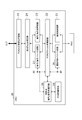
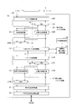
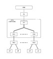
- FIG. 1 is a block diagram illustrating a configuration of a wireless network system according to the first embodiment.
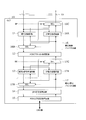
- FIG. 2 is a block diagram illustrating a configuration of the OLT according to the first embodiment.
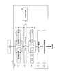
- FIG. 3 is a block diagram illustrating the configuration of the ONU according to the first embodiment.
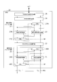
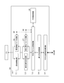
- FIG. 4 is a block diagram illustrating a configuration of the OLT according to the second embodiment.
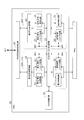
- FIG. 5 is a block diagram illustrating a configuration of an ONU according to the second embodiment.
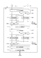
- FIG. 6 is a block diagram illustrating a configuration of an OLT according to the third embodiment.
- FIG. 7 is a block diagram illustrating a configuration of an ONU according to the third embodiment.
- FIG. 8 is a block diagram illustrating a configuration of an OLT according to the fourth embodiment.
- FIG. 1 is a block diagram illustrating a configuration of a wireless network system according to the first embodiment.
- FIG. 2 is a block diagram illustrating a configuration of the OLT according to the first embodiment.
- FIG. 9 is a block diagram illustrating a configuration of an ONU according to the fourth embodiment.
- FIG. 10 is a block diagram illustrating a configuration of an OLT according to the fifth embodiment.
- FIG. 11 is a block diagram illustrating a configuration of an ONU according to the fifth embodiment.
- FIG. 12 is a block diagram illustrating a configuration of an OLT according to the sixth embodiment.
- FIG. 13 is a block diagram illustrating a configuration of an ONU according to the sixth embodiment.
- FIG. 14 is a block diagram illustrating a configuration of an OLT according to the seventh embodiment.
- FIG. 15 is a block diagram illustrating a configuration of an ONU according to the seventh embodiment.
- FIG. 16 is a configuration example of a general wireless network system.
- FIG. 17 is an explanatory diagram showing the MFH layer 2 conversion.
- FIG. 18 is a configuration example of MFH to which TDM-PON is applied.
- this radio network system 1 includes one central station CU (Central Unit) and one or more radio stations RRU that perform radio communication with one or more user terminals UE accommodated therein. (Remote Radio Unit) and a mobile front hole MFH (Mobile Fronthaul) that connects the CU and the RRU.
- Central Unit Central Unit
- RRU Radio Unit
- MFH Mobile Fronthaul
- the radio network system 1 is a system that transfers data transmitted and received by the UE between the CU and RRU via the MFH by dividing and executing a plurality of radio protocol processes by the CU and RRU.
- the invention applies the PON system 2 as MFH.
- the PON system 2 is composed of one station-side device OLT 10 that is a PON device and a plurality of subscriber-side devices ONU 20 that accommodates one or a plurality of RRUs under the control, and through the PON composed of optical fibers, This is an optical access network system that transfers data in a time-sharing manner between the OLT 10 and the ONU 20.
- FIG. 1 shows an example in which only one RRU is accommodated under the ONU and only one UE is connected to the RRU for easy understanding. It is not limited to this. In general, one or more RRUs are accommodated in the ONU, and one or more UEs are connected to each RRU.
- the CU, RRU, and UE have a generally known configuration, and detailed description thereof is omitted here.
- TDM-PON which is a TDM type PON system
- present invention is not limited to this, and other types of PON systems may be used. Can be applied in the same manner, and similar effects can be obtained.
- the PON system 2 according to the present invention will be described as an example in which the PON system 2 is used as the MFH of the wireless network system 1 that operates based on wireless protocol processing, but is not limited thereto.
- the PON system 2 according to the present invention can also be used when an arbitrary section is relay-connected by optical communication. Similar effects can be obtained.
- the CU and RRU correspond to a host device and a home gateway.
- a priority control circuit 11 As a main circuit unit, a priority control circuit 11, a PON protocol processing circuit 12, an encryption / decryption processing circuit 13, and an error correction processing circuit 14 having the same configuration as that of FIG.
- a priority control bypass circuit 16 and an encryption / decryption bypass circuit 17 are provided.
- These circuit units are composed of one or a plurality of semiconductor chips. Note that some of the functions of priority control, PON protocol processing, and encryption / decryption processing can be configured by software on the CPU in the OLT.
- the ONU 20 includes, as main circuit units, a priority control circuit 21, a PON protocol processing circuit 22, an encryption / decryption processing circuit 23, an error correction process, which have the same configuration as that of FIG.
- a priority control bypass circuit 26 and an encryption / decryption bypass circuit 27 are provided.
- These circuit units are composed of one or a plurality of semiconductor chips. Note that some of the functions of priority control, PON protocol processing, and encryption / decryption processing can be configured by software on the CPU in the ONU.
- the priority control bypass circuit 16 has a function of bypassing data input to the priority control circuit 11 in accordance with a preset priority control bypass instruction BP.
- the encryption / decryption bypass circuit 17 has a function of bypassing data input to the encryption / decryption processing circuit 13 in accordance with a preset encryption / decryption bypass instruction BE.
- the priority control bypass circuit 16 and the encryption / decryption bypass circuit 17 perform bypass processing on both downlink data from the CU to the UE and uplink data from the UE to the CU.
- the priority control bypass circuit 26 has a function of bypassing data input to the priority control circuit 21 in accordance with a preset priority control bypass instruction BP.
- the encryption / decryption bypass circuit 27 has a function of bypassing data input to the encryption / decryption processing circuit 23 in accordance with a preset encryption / decryption bypass instruction BE.
- the priority control bypass circuit 26 and the encryption / decryption bypass circuit 27 perform bypass processing on both downlink data from the CU to the UE and uplink data from the UE to the CU.
- the priority control circuit 11 and the priority control circuit 21 operate as a pair, and by performing priority control processing on data transferred between the OLT 10 and the ONU 20 via the PON, in the PON section This is to ensure communication quality.
- the encryption / decryption processing circuit 13 and the encryption / decryption processing circuit 23 operate as a pair, and by performing encryption / decryption processing on data transferred between the OLT 10 and the ONU 20 via the PON, This is to ensure security in the PON section.
- the PON protocol processing circuit 12, the error correction processing circuit 14, the PON optical transmission / reception processing circuit 15, and the PON protocol processing circuit 22, the error correction processing circuit 24, and the PON optical transmission / reception processing circuit 25 are generally known configurations. The detailed description here is omitted.
- the wireless protocol processing used in the wireless network system 1 performs encryption / decryption processing in addition to packet header compression / decompression processing as shown in FIG. It has become.
- the encryption / decryption processing in PDCP corresponds to the encryption / decryption processing executed in the UE, and is for ensuring security in the path between the PDCP and the UE.
- the MAC performs priority control processing in addition to processing such as radio resource allocation, data mapping, and retransmission control.
- the priority control process in the MAC corresponds to the priority control process executed in the UE, and is for ensuring the communication quality in the path between the MAC and the UE.
- the station side device OLT 10 and the subscriber side device ONU 20 constituting the PON system 2 used as the MFH can transmit and receive data via a PON made of an optical fiber.
- An encryption / decryption processing circuit that performs encryption / decryption processing and a priority control circuit that performs priority control processing on the data are provided. Therefore, the encryption / decryption process and the priority control process in the OLT 10 and the ONU 20 overlap with the encryption / decryption process and the priority control process in the PDCP and MAC among the wireless protocol processes.
- a division point may be provided between arbitrary processes from PDCP to RF.
- MFH will be inserted into. Therefore, for example, in the case of the MAC-PHY division method, MFH is inserted between the MAC and PHY, so that data transferred by MFH is encrypted / decrypted in PDCP and MAC and priority control.
- the encryption / decryption processing and the priority control processing in the OLT 10 and the ONU 20 are executed in duplicate in the MFH section.
- the present invention can reduce processing delays in the OLT 10 and the ONU 20 by bypassing the encryption / decryption processing and priority control processing that are executed redundantly on data transferred by such MFH, and Note that these overlapping processes change depending on the position of the division point of the wireless protocol process. Then, the OLT 10 and the ONU 20 are provided with a bypass circuit that bypasses one or both of the encryption / decryption process and the priority control process, and based on a bypass instruction set in advance according to the division point position of the wireless protocol process, Switching between bypass / non-bypass in the bypass circuit is controlled.
- the priority control bypass circuit 16 is provided with an IF matching processing circuit 16A and selectors SEL16B and 16C as main processing circuits.
- the encryption / decryption bypass circuit 17 is provided with an IF matching processing circuit 17A and selectors SEL17B and 17C as main processing circuits.
- the IF matching processing circuit 16A takes in the downlink input data that is output from the CU and is input to the priority control circuit 11 to be bypassed, and sets an interface such as a standard or a format related to the downlink input data as the downlink input data. By matching with downlink non-bypass data obtained by applying priority control processing, it has a function of generating downlink bypass data that bypasses priority control processing.
- the IF matching processing circuit 16A takes in the upstream input data output from the PON protocol processing circuit 12 and is input to the priority control circuit 11 to be bypassed, and interfaces such as standards and formats related to the upstream input data. Is matched with uplink non-bypass data obtained by applying priority control processing to uplink input data, and has a function of generating uplink bypass data that bypasses priority control processing.
- the SEL 16B switches and selects either the downlink non-bypass data output from the priority control circuit 11 or the downlink bypass data output from the IF matching processing circuit 16A to select the PON protocol. It has a function of outputting to the processing circuit 12.
- the SEL 16C switches and selects either the uplink non-bypass data output from the priority control circuit 11 or the uplink bypass data output from the IF matching processing circuit 16A to the CU. It has a function to output.
- the priority control bypass instruction BP indicates non-bypass
- the downlink non-bypass data output from the priority control circuit 11 in SEL 16B is selected and output to the PON protocol processing circuit 12, and the priority control circuit 11 in SEL 16C.
- the uplink non-bypass data output from is selected and output to the CU.
- the priority control bypass instruction BP indicates bypass
- the downlink bypass data output from the IF matching processing circuit 16A by the SEL 16B is selected and output to the PON protocol processing circuit 12, and the IF matching processing circuit 16A is selected by the SEL 16C.
- the uplink bypass data output from is selected and output to the CU.
- the IF matching processing circuit 17A takes in the downstream input data that is output from the PON protocol processing circuit 12 and is input to the encryption / decryption processing circuit 13 to be bypassed, and an interface such as a standard and format related to the downstream input data. Has the function of generating downlink bypass data that bypasses the encryption / decryption process by matching the downlink non-bypass data obtained by applying the encryption / decryption process to the downlink input data. Yes.
- the IF matching processing circuit 17A takes in the upstream input data that is output from the error correction processing circuit 14 and is input to the encryption / decryption processing circuit 13 to be bypassed, and a standard or format related to the upstream input data. Has a function to generate uplink bypass data that bypasses the encryption / decryption processing by matching the interface with the uplink non-bypass data obtained by applying the encryption / decryption processing to the uplink input data. is doing.
- the SEL 17B switches and selects either the downlink non-bypass data output from the encryption / decryption processing circuit 13 or the downlink bypass data output from the IF matching processing circuit 17A in response to the encryption / decryption bypass instruction BE.
- the SEL 17C switches and selects either the uplink non-bypass data output from the encryption / decryption processing circuit 13 or the uplink bypass data output from the IF matching processing circuit 17A in response to the encryption / decryption bypass instruction BE.
- the encryption / decryption bypass instruction BE indicates non-bypass
- the downlink non-bypass data output from the encryption / decryption processing circuit 13 is selected by the SEL 17B and output to the error correction processing circuit 14, and the encryption is performed by the SEL 17C.
- / Upstream non-bypass data output from the decoding processing circuit 13 is selected and output to the PON protocol processing circuit 12.
- the encryption / decryption bypass instruction BE indicates bypass
- the downlink bypass data output from the IF matching processing circuit 17A is selected by the SEL 17B and output to the error correction processing circuit 14, and the IF matching processing circuit is selected by the SEL 16C.
- the uplink bypass data output from 17A is selected and output to the PON protocol processing circuit 12.
- the priority control bypass circuit 26 is provided with an IF matching processing circuit 26A and selectors SEL 26B and 26C as main processing circuits.
- the encryption / decryption bypass circuit 27 is provided with an IF matching processing circuit 27A and selectors SEL27B and 27C as main processing circuits.
- the IF matching processing circuit 26A takes in the upstream input data that is output from the RRU and is input to the priority control circuit 21 to be bypassed, and converts an interface such as a standard or format related to the upstream input data to the upstream input data. By matching with uplink non-bypass data obtained by applying priority control processing, it has a function of generating uplink bypass data that bypasses priority control processing.
- the IF matching processing circuit 26A takes in the downlink input data output from the PON protocol processing circuit 12 and is input to the priority control circuit 21 to be bypassed, and interfaces such as standards and formats related to the downlink input data. Is matched with downlink non-bypass data obtained by applying priority control processing to downlink input data, thereby having a function of generating downlink bypass data that bypasses priority control processing.
- the SEL 26B switches and selects either the uplink non-bypass data output from the priority control circuit 21 or the uplink bypass data output from the IF matching processing circuit 26A. It has a function of outputting to the processing circuit 22.
- the SEL 26C switches and selects one of the downlink non-bypass data output from the priority control circuit 21 and the downlink bypass data output from the IF matching processing circuit 26A, and sends it to the RRU. It has a function to output.
- the priority control bypass instruction BP indicates non-bypass
- the uplink non-bypass data output from the priority control circuit 21 in SEL 26B is selected and output to the PON protocol processing circuit 22, and the priority control circuit 21 in SEL 26C.
- the downlink non-bypass data output from is selected and output to the RRU.
- the priority control bypass instruction BP indicates bypass
- the upstream bypass data output from the IF matching processing circuit 26A by the SEL 26B is selected and output to the PON protocol processing circuit 22, and the IF matching processing circuit 26A is selected by the SEL 26C.
- the downlink bypass data output from is selected and output to the RRU.
- the IF matching processing circuit 27A takes in the upstream input data output from the PON protocol processing circuit 22 and is input to the encryption / decryption processing circuit 23 to be bypassed, and interfaces such as standards and formats related to the upstream input data. Has a function of generating uplink bypass data that bypasses the encryption / decryption processing by matching the uplink non-bypass data obtained by applying the encryption / decryption processing to the uplink input data. Yes.
- the IF matching processing circuit 27A takes in the downstream input data output from the error correction processing circuit 24 and is input to the encryption / decryption processing circuit 23 to be bypassed, and the standards and formats relating to the downstream input data.
- the SEL 27B switches and selects either the uplink non-bypass data output from the encryption / decryption processing circuit 23 or the uplink bypass data output from the IF matching processing circuit 27A. And a function of outputting to the error correction processing circuit 24.
- the SEL 27C switches and selects either downlink non-bypass data output from the encryption / decryption processing circuit 23 or downlink bypass data output from the IF matching processing circuit 27A. A function of outputting to the PON protocol processing circuit 22.
- the encryption / decryption bypass instruction BE indicates non-bypass
- the uplink non-bypass data output from the encryption / decryption processing circuit 23 is selected by the SEL 27B and output to the error correction processing circuit 24, and the encryption is performed by the SEL 27C.
- / Downstream non-bypass data output from the decoding processing circuit 23 is selected and output to the PON protocol processing circuit 22.
- the encryption / decryption bypass instruction BE indicates bypass
- the upstream bypass data output from the IF matching processing circuit 27A is selected by the SEL 27B and output to the error correction processing circuit 24, and the IF matching processing circuit is selected by the SEL 26C.
- the downlink bypass data output from 27A is selected and output to the PON protocol processing circuit 22.
- the OLT 10 is provided with the priority control bypass circuit 16 and the encryption / decryption bypass circuit 17, and encryption is performed according to the preset priority control bypass instruction BP and encryption / decryption bypass instruction BE. / Either or both of the decoding process and the priority control process are bypassed.
- the ONU 20 is provided with a priority control bypass circuit 26 and an encryption / decryption bypass circuit 27, and encryption / decryption processing and priority control processing are performed in accordance with a preset priority control bypass instruction BP and encryption / decryption bypass instruction BE. One or both of them are bypassed.
- the priority control bypass circuit 16 and the encryption / decryption bypass circuit 17 of the OLT 10 and the priority control bypass circuit 26 and the encryption / decryption bypass circuit 27 of the ONU 20 have been described on the assumption that they are provided as a pair.
- the present invention is not limited to this. If only one of them can reduce the processing delay, there is no need to provide a pair.
- the radio network system 1 Next, a radio network system 1 according to the second exemplary embodiment of the present invention will be described.
- the priority control bypass instruction BP and the encryption / decryption bypass instruction BE are set in advance has been described.
- the OLT 10 or ONU 20 identifies the division point of the wireless protocol processing divided in advance by the CU and RRU based on the control information given to the data from the CU or RRU, and performs priority control bypass.
- a case where the instruction BP and the encryption / decryption bypass instruction BE are generated autonomously will be described.
- the priority control bypass circuit 16 of the OLT 10 according to the present embodiment is added with a bypass control circuit 16 ⁇ / b> D as compared with FIG. 2, and the encryption / decryption bypass circuit 17 similarly includes A bypass control circuit 17D is added.
- the bypass control circuit 16D has a function of identifying the position of the division point of the radio protocol processing divided in advance by the CU and the RRU from the control information included in the downlink data output from the CU or the uplink data output from the UE, It has a function of generating a priority control bypass instruction BP according to the obtained position of the dividing point and outputting it to the SELs 16B and 16C.
- the bypass control circuit 17D has a function of identifying the position of the division point of the radio protocol processing divided in advance by the CU and RRU from the control information included in the downlink data output from the CU or the uplink data output from the UE,
- the encryption / decryption bypass instruction BE is generated according to the obtained position of the dividing point and output to the SELs 17B and 17C.
- the bypass instruction generation processing in the bypass control circuit 16D and the bypass control circuit 17D is set in advance with new tag information indicating the division point position given to the uplink data or downlink data as control information by the CU or RRU.
- the priority control bypass instruction BP and the encryption / decryption bypass instruction BE may be generated.
- 2-bit instruction data “11” (binary value) is set in the table corresponding to the tag value “0” indicating the MAC-PHY division method, and the tag value “1” indicating the PDCP-RLC division method is set.
- 2-bit instruction data “01” may be set in the table.
- the upper bits of the instruction data correspond to priority control bypass instructions BP (1... Bypass, 0... Non-bypass), and the lower bits correspond to encryption / decryption bypass instructions BE (1... Bypass, 0. . Therefore, when the acquired tag value is “0” indicating the MAC-PHY division method, the priority control bypass instruction BP for instructing “bypass” and the encryption / decryption bypass based on the instruction data “11” obtained from the table An instruction BE is output. When the acquired tag value is “1” indicating the PDCP-RLC division method, the priority control bypass instruction BP instructing “non-bypass” and the “bypass” based on the instruction data “01” obtained from the table. The encryption / decryption bypass instruction BE for instructing is output.
- control information that replaces the tag value As control information that replaces the tag value, existing control information stored in the uplink data or downlink data for control exchanged between the CU and the RRU is extracted, and the table is referred to in the same manner as the tag value.
- the priority control bypass instruction BP and the encryption / decryption bypass instruction BE may be generated.
- the bypass control circuit 16D identifies the division point position of the radio protocol processing based on the downlink data from the CU or the uplink data from the UE, and the priority control bypass instruction BP corresponding to the division point position is selected by the SEL 16B, Is output to 16C. Further, the bypass control circuit 17D identifies the division point position of the radio protocol processing based on the downlink data from the CU or the uplink data from the UE, and the encryption / decryption bypass instruction BE corresponding to the division point position is SEL 17B, To 17C.
- the bypass control circuit 26D has a function of identifying the position of the division point of the radio protocol processing divided in advance by the CU and the RRU from the control information included in the downlink data output from the CU or the uplink data output from the UE; It has a function of generating a priority control bypass instruction BP according to the position of the obtained dividing point and outputting it to the SELs 26B and 26C.
- the bypass control circuit 27D has a function of identifying the position of the division point of the radio protocol processing divided in advance by the CU and RRU from the control information included in the downlink data output from the CU or the uplink data output from the UE,
- the encryption / decryption bypass instruction BE is generated according to the position of the obtained dividing point and output to the SELs 27B and 27C.
- the bypass control circuit 26D identifies the division point position of the radio protocol processing based on the downlink data from the CU or the uplink data from the UE, and the priority control bypass instruction BP corresponding to the division point position is selected by the SEL 26B, To 26C. Further, the bypass control circuit 27D identifies the division point position of the radio protocol processing based on the downlink data from the CU or the uplink data from the UE, and the encryption / decryption bypass instruction BE corresponding to the division point position is sent to the SEL 27B, To 27C.
- the bypass instruction generation processing in the bypass control circuit 26D and the bypass control circuit 27D is the same as that of the bypass control circuit 16D and the bypass control circuit 17D described above.
- the ONU identifies the division point position of the wireless protocol processing based on the downlink data
- the processing circuit is equipped with not only a function to decrypt and transfer encrypted data but also a function to transfer unencrypted data as it is, and it can be identified by setting the initial state of ONU encryption / decryption bypass instruction BE to non-bypass. It becomes.
- the division point may be identified based on the downlink data for control generated and transmitted by the OLT instead of the data from the CU or the UE.
- the bypass control circuit 26D of FIG. 5 is arranged on the RRU side, it can also be arranged on the PON protocol processing circuit side.
- the bypass control circuit 16D and the bypass control circuit 26D identify the division point position of the radio protocol processing based on the downlink data from the CU or the uplink data from the UE, and the division point.
- the priority control bypass instruction BP corresponding to the position is generated, and the bypass control circuit 17D and the bypass control circuit 27D identify the division point position of the radio protocol processing based on the downlink data from the CU or the uplink data from the UE.
- the encryption / decryption bypass instruction BE corresponding to the division point position is generated.
- the priority control bypass instruction BP and the encryption / decryption bypass instruction BE are autonomously generated based on the division points of the wireless protocol processing divided in advance by the CU and the RRU. Therefore, the priority control bypass instruction BP and the encryption / decryption bypass instruction BE do not need to be set in advance, and the priority control bypass instruction BP and the encryption / decryption bypass instruction BE are dynamically changed according to the operation of the system. Is possible.
- the PON protocol processing circuit 12 of the OLT 10 and the PON protocol processing circuit 22 of the ONU 20 control optical data communication in the PON section such as dynamic bandwidth allocation for each ONU 20, for example, based on a dedicated PON protocol.
- OMCC ONU Management and Control Channel
- NG-PON2 Next Generation-PON2
- uplink / downlink data exchanged between the OLT 10 and the ONU 20 is based on the encryption / decryption bypass instruction BE and the priority control bypass instruction BP. Not applicable is determined. Therefore, in the configuration example of FIG. 1, the control data transmitted and received by the PON protocol processing circuit 12 and the PON protocol processing circuit 22 depend on whether the bypass is applied or not applied to the uplink / downlink data.
- control data transmitted from the PON protocol processing circuit 12 of the OLT 10 to the PON side bypasses the encryption / decryption processing circuit 13 by the encryption / decryption bypass circuit 17. It is transmitted to the PON side.
- control data that is not encrypted is exchanged in the PON section, and encryption of control data defined by OMCC cannot be satisfied.
- the control data is encrypted in advance, if the encryption / decryption process is not bypassed, the encryption for the control data will be duplicated, increasing the processing load and delay. The same applies to the ONU 20.
- the downstream PON protocol processing circuit 12 of the OLT 10 needs to determine which of the OMCC control data and the data from the CU is prioritized and transmit it to the PON side.
- the description of this function is omitted.
- priority control processing when waiting for data transfer from the CU due to transfer of OMCC control data, priority is given to the data transferred next to the control data being transferred from among the data from the CU.
- the data having the highest degree is selected and transferred, or when the priority of the data of the next OMCC is higher than the priority of the data from the CU, the data of the next OMCC is transferred.
- the priority control process is bypass application, the order of data transfer does not need to consider the priority.
- the OMCC control data encryption is performed by placing the OMCC transmission at the head of the FS payload defined by NG-PON2. Therefore, the priority control process in the PON protocol processing circuit 12 needs to be changed so that the PON control circuit can perform the conversion. Details will be described later. The same applies to the ONU 20.
- the OLT 10 includes a control encryption / decryption processing circuit 18 that performs encryption / decryption processing on control data used for control of the PON system 2.
- the PON protocol processing circuit 12 exchanges according to the presence / absence of bypass for the encryption / decryption processing in the encryption / decryption bypass circuit 17, specifically, according to the encryption / decryption bypass instruction BE.
- the application / non-application of encryption / decryption processing to control data to be switched is switched.
- the PON protocol processing circuit 12 sends the encryption / decryption processing circuit 13 to the encryption / decryption processing circuit 13 according to whether or not the priority control processing is bypassed in the priority control bypass circuit 16, specifically, according to the priority control bypass instruction BP. Whether or not the control for each priority regarding the output data is executed in the PON protocol processing circuit 12 is switched. In the OLT 10, the PON protocol processing circuit 12 determines whether the priority control bypass circuit 16 bypasses the priority control process, specifically, to the priority control bypass circuit 16 according to the priority control bypass instruction BP. The output permission is output or the output permission is output to the priority control circuit 11.
- control encryption / decryption processing circuit 18 is provided as hardware and provided between the PON control circuit 19 that controls the PON system 2 and the PON protocol processing circuit 12 will be described as an example. It is not limited to this.
- the control encryption / decryption processing circuit 18 may be mounted (hardware / software) inside the PON protocol processing circuit 12 or the PON control circuit 19.
- a control encryption / decryption processing circuit 18 may be provided between the OLT 10 and the external device or inside the external device.
- Other configurations of the OTL 10 according to the present embodiment are the same as those of the first and second embodiments described above, and a description thereof is omitted here.
- the ONU 20 is provided with a control encryption / decryption processing circuit 28 for performing encryption / decryption processing on control data used for control of the PON system 2.
- the encryption / decryption processing circuit 28 uses the PON protocol processing circuit 22 according to the presence / absence of bypass for the encryption / decryption processing in the encryption / decryption bypass circuit 27, specifically, according to the encryption / decryption bypass instruction BE. In this case, the application / non-application of the encryption / decryption processing to the control data exchanged by the user is switched.
- the PON protocol processing circuit 22 sends the encryption / decryption processing circuit 23 to the encryption / decryption processing circuit 23 according to the presence / absence of bypass of the priority control process in the priority control bypass circuit 26, specifically, according to the priority control bypass instruction BP. Whether or not the control for each priority regarding the output data is executed in the PON protocol processing circuit 22 is switched. In the ONU 20, the PON protocol processing circuit 22 determines whether or not the priority control processing in the priority control bypass circuit 26 is bypassed, specifically, to the priority control bypass circuit 26 according to the priority control bypass instruction BP. The output permission is outputted or the output permission is outputted to the priority control circuit 21.
- control encryption / decryption processing circuit 28 is provided as hardware and provided between the PON control circuit 29 that controls the PON system 2 and the PON protocol processing circuit 22 will be described as an example. It is not limited to this.
- the control encryption / decryption processing circuit 28 may be mounted inside the PON protocol processing circuit 22 or the PON control circuit 29 (hardware / software).
- the control encryption / decryption processing circuit 28 may be provided between the ONU 20 and the external device or inside the external device.
- Other configurations of the ONU 20 according to this embodiment are the same as those in the first and second embodiments described above, and a description thereof is omitted here.
- priority control is performed on downlink wireless user data in the MAC process, and wireless user data is encrypted in the PDCP process. That is, the downlink data after priority control and encryption are performed by the CU transmits the MFH. For this reason, the OLT 10 and the ONU 20 in the present embodiment bypass downlink priority control and encryption processing that overlap with the CU.
- the upstream control from the ONU 20 to the OLT 10 similarly bypasses priority control and decoding processing. This is because the uplink data from the RRU is data after being encrypted and preferentially controlled by the user terminal (UE) or RRU.
- the PON protocol processing circuit 12 receives the uplink data and the uplink control data (OMCC control data) from the encryption / decryption bypass circuit 17. Among these, the uplink control data is output to the control encryption / decryption processing circuit 18, and the uplink data other than the uplink control data is output to the upper unit (CU) side.
- OMCC control data uplink control data
- CU upper unit
- the PON protocol processing circuit 12 adds decoding information such as SFC (SuperFrame Counter) and IFC (Intra-Frame Counter) necessary for decoding the uplink control data to the uplink control data and outputs it.
- decoding information such as SFC (SuperFrame Counter) and IFC (Intra-Frame Counter) necessary for decoding the uplink control data to the uplink control data and outputs it.
- the uplink control data is decrypted by the control encryption / decryption processing circuit 18 based on the decryption information, and then used for the control of the PON system 2 by the PON control circuit 19. Further, uplink data other than the uplink control data is output from the OLT 10 to the host device side via the priority control bypass circuit 16.
- the PON protocol processing circuit 12 downloads the downlink data from the priority control bypass circuit 16 and the downlink control data output from the PON control circuit 19 and encrypted by the control encryption / decryption processing circuit 18. And the downstream data and downstream control data from the priority control bypass circuit 16 are inserted into the FS payload and output to the PON side. As a result, the downlink data and downlink control data from the priority control bypass circuit 16 are output to the error correction processing circuit 14 via the encryption / decryption bypass circuit 17.
- the PON protocol processing circuit 12 inserts the downlink control data at the head position of the FS payload, and then inserts the downlink data from the priority control bypass circuit 16 at the subsequent position.
- IFC can be determined from the FS header length managed by software.
- the software specifies the SFC of the PHY frame that transmits the header when generating the FS header, and uses the SFC at the time of IFC determination (the SFC of the PHY frame into which the FS payload is inserted). do it.
- a buffer for downlink data from the priority control bypass circuit 16 is mounted in the PON protocol processing circuit 12, or a priority control bypass circuit is included in the PON protocol processing circuit 12. It is only necessary to provide a function for permitting the output to 16 and permit the output to the priority control bypass circuit 16 only when downlink data is inserted from the priority control bypass circuit 16. In the latter case, a buffer is mounted in the priority control bypass circuit 16, and when the output permission is input from the PON protocol processing circuit 12, the priority control bypass circuit 16 outputs data from the buffer.
- the PON protocol processing circuit 22 transmits upstream data from the priority control bypass circuit 26 and upstream control data output from the PON control circuit 29 and encrypted by the control encryption / decryption processing circuit 28. And the downlink data and downlink control data from the priority control bypass circuit 26 having the same Allocation-ID are inserted into the same FS payload and output to the PON side.
- the PON protocol processing circuit 22 inserts the uplink control data of the Allocation-ID at the head position of the FS payload, and then transmits the uplink data from the priority control bypass circuit 26 of the Allocation-ID. Insert at the subsequent position.
- the uplink data and the uplink control data from the priority control bypass circuit 26 are output to the error correction processing circuit 24 via the encryption / decryption bypass circuit 27.
- uplink data from the priority control bypass circuit 26 may be inserted from the head position of the FS payload.
- the PON protocol processing circuit 22 inserts the uplink control data at the head position of the FS payload for the uplink data and the uplink control data from the priority control bypass circuit 26 of the same Allocation-ID, and then the priority control bypass.
- the upstream data from the circuit 26 is inserted at the subsequent position.
- IFC can be determined from uplink bandwidth allocation information (BWmap StartTime / GrantSize / DBRu presence / absence / PLOAMu presence / absence).
- the SFC value corresponding to BWmap may be used so that the software can manage it.
- a buffer for the uplink data from the priority control bypass circuit 26 is installed in the PON protocol processing circuit 22 for each Allocation-ID, or in the PON protocol processing circuit 22. Is equipped with a function for permitting output to the priority control bypass circuit 26 (and a function for outputting Allocation-ID information for permitting output), and priority control is performed only when uplink data is inserted from the priority control bypass circuit 26. What is necessary is just to permit an output to the bypass circuit 26.
- a buffer is mounted for each Allocation-ID in the priority control bypass circuit 26, and the priority control bypass circuit 26 receives an output permission (and information on the permitted Allocation-ID) from the PON protocol processing circuit 22. If so, the data is output from the permitted Allocation-ID buffer.
- the PON protocol processing circuit 22 receives downlink data and downlink control data from the encryption / decryption bypass circuit 27. Among these, the downlink control data is output to the control encryption / decryption processing circuit 28, and the downlink data other than the downlink control data is output to the user terminal side.
- the PON protocol processing circuit 22 adds the decoding information such as SFC and IFC necessary for decoding the downlink control data to the downlink control data and outputs it.
- the downlink control data is decrypted based on the decryption information by the control encryption / decryption processing circuit 28 and then used for controlling the PON system 2 by the PON control circuit 29.
- downlink data other than downlink control data is output from the ONU 20 to the user terminal side via the priority control bypass circuit 26.
- the PON protocol processing circuit 12 receives the uplink data and the uplink control data from the encryption / decryption bypass circuit 17. Among these, the uplink control data is output to the control encryption / decryption processing circuit 18, and the uplink data other than the uplink control data is output to the upper unit (CU) side.
- CU unit
- the PON protocol processing circuit 12 adds decoding information such as SFC and IFC necessary for decoding the uplink control data to the uplink control data and outputs it.
- the uplink control data is decrypted by the control encryption / decryption processing circuit 18 based on the decryption information, and then used for the control of the PON system 2 by the PON control circuit 19.
- uplink data other than the uplink control data is output from the OLT 10 to the host device side via the priority control circuit 11.
- the PON protocol processing circuit 12 Downstream In the OLT 10, the PON protocol processing circuit 12 includes downstream data from the priority control circuit 11, downstream control data output from the PON control circuit 19 and encrypted by the control encryption / decryption processing circuit 18, and , And the downlink data and downlink control data from the priority control circuit 11 are inserted into the FS payload and output to the PON side. As a result, the downlink data and downlink control data from the priority control circuit 11 are output to the error correction processing circuit 14 via the encryption / decryption bypass circuit 17.
- the PON protocol processing circuit 12 inserts the downlink control data at the head position of the FS payload, and then inserts the downlink data from the priority control circuit 11 at the subsequent position.
- IFC can be determined from the FS header length managed by software.
- the software specifies the SFC of the PHY frame that transmits the header when generating the FS header, and uses the SFC at the time of IFC determination (the SFC of the PHY frame into which the FS payload is inserted). do it.
- a buffer for each priority level is mounted in the PON protocol processing circuit 12 so that priority is given to the output from the high priority buffer (insertion into the FS payload), or in the PON protocol processing circuit 12.
- a function for permitting the output to the priority control circuit 11 is provided, and the output to the priority control circuit 11 may be permitted only when downlink data is inserted from the priority control circuit 11. In the latter case, a buffer for each priority in the priority control circuit 11 is used.
- the PON protocol processing circuit 22 includes upstream data from the priority control circuit 21, upstream control data output from the PON control circuit 29 and encrypted by the control encryption / decryption processing circuit 28, and And the upstream data and the upstream control data from the priority control circuit 21 having the same Allocation-ID are inserted into the same FS payload and output to the PON side.
- the PON protocol processing circuit 22 inserts the uplink control data of the Allocation-ID at the head position of the FS payload, and then transmits the uplink data from the priority control circuit 21 of the Allocation-ID. Insert in the continuation position.
- the uplink data and the uplink control data from the priority control circuit 21 are output to the error correction processing circuit 24 via the encryption / decryption bypass circuit 27.
- upstream data from the priority control circuit 21 may be inserted from the head position of the FS payload.
- the PON protocol processing circuit 22 inserts the uplink control data at the head position of the FS payload for the uplink data and the uplink control data from the priority control circuit 21 having the same Allocation-ID, and then the priority control circuit 21.
- the upstream data from is inserted at the subsequent position.
- IFC can be determined from uplink bandwidth allocation information (BWmap StartTime / GrantSize / DBRu presence / absence / PLOAMu presence / absence).
- the SFC value corresponding to BWmap may be used so that the software can manage it.
- a buffer for each priority is mounted in the PON protocol processing circuit 22 for each Allocation-ID so that priority is given to output from the buffer with high priority (insertion into the FS payload) or PON.
- a function for permitting output to the priority control circuit 21 in the protocol processing circuit 22 (and a function for outputting information of Allocation-ID permitting output) is mounted, and when uplink data is inserted from the priority control circuit 21 Only the priority control circuit 21 needs to be allowed to output.
- a buffer for each priority is mounted for each Allocation-ID in the priority control circuit 21, and the priority control circuit 21 permits output from the PON protocol processing circuit 22 (and information on the permitted Allocation-ID). Is given priority, the output from the buffer with the higher priority of Allocation-ID permitted is output.
- the priority control circuit 21 permits output from the PON protocol processing circuit 22 (and information on the permitted Allocation-ID). Is given priority, the output from the buffer with the higher priority of Allocation-ID permitted is output.
- the PON protocol processing circuit 22 receives downlink data and downlink control data from the encryption / decryption bypass circuit 27. Among these, the downlink control data is output to the control encryption / decryption processing circuit 28, and the downlink data other than the downlink control data is output to the user terminal side.
- the PON protocol processing circuit 22 adds the decoding information such as SFC and IFC necessary for decoding the downlink control data to the downlink control data and outputs it.
- the downlink control data is decrypted based on the decryption information by the control encryption / decryption processing circuit 28 and then used for controlling the PON system 2 by the PON control circuit 29.
- downlink data other than downlink control data is output from the ONU 20 to the user terminal side via the priority control circuit 21.
- OLT Uplink
- the PON protocol processing circuit 12 receives the uplink data and the uplink control data from the encryption / decryption processing circuit 13. Among these, the uplink control data is output to the control encryption / decryption processing circuit 18, and the uplink data other than the uplink control data is output to the upper unit (CU) side.
- the control encryption / decryption processing circuit 18 outputs the uplink control data to the PON control circuit 19 as it is without decrypting it. Further, uplink data other than the uplink control data is output from the OLT 10 to the host device side via the priority control circuit 11.
- the PON protocol processing circuit 12 downloads the downlink data from the priority control circuit 11 and the downlink control data output from the PON control circuit 19 and not encrypted by the control encryption / decryption processing circuit 18. And the downstream data and downstream control data from the priority control circuit 11 are inserted into the FS payload and output to the PON side. As a result, the downlink data and downlink control data from the priority control circuit 11 are output to the error correction processing circuit 14 via the encryption / decryption processing circuit 13.
- a buffer for each priority level is mounted in the PON protocol processing circuit 12 so that priority is given to the output from the high priority buffer (insertion into the FS payload), or in the PON protocol processing circuit 12.
- the downlink data and the downlink control data from the priority control circuit 11 are stored in the same buffer according to the priority, or the downlink data buffer and the downlink control data from the priority control circuit 11 are stored.
- the buffers may be alternately inserted into the FS payload. .
- the PON protocol processing circuit 12 determines, by setting or the like, how often the downlink data or the downlink control data from the priority control circuit 11 is inserted, and the downlink control data is transferred to the FS payload. When inserting, it inserts from the buffer for downlink control data in the PON protocol processing circuit 12 according to the priority, and when inserting the downlink data from the priority control circuit 11 into the FS payload, the priority in the priority control circuit 11 When the output permission is input from the PON protocol processing circuit 12, the priority control circuit 11 gives priority to the output from the buffer having a high priority. In either case of the former or the latter case, the insertion of the downlink control data into the FS payload may be given priority over the insertion of the downlink data from the priority control circuit 11.
- the PON protocol processing circuit 22 transmits upstream data from the priority control circuit 21, and upstream control data output from the PON control circuit 29 and not encrypted by the control encryption / decryption processing circuit 28. And the upstream data and the upstream control data from the priority control circuit 21 having the same Allocation-ID are inserted into the same FS payload and output to the PON side.
- a buffer for each priority is mounted in the PON protocol processing circuit 22 for each Allocation-ID so that priority is given to output from the buffer with high priority (insertion into the FS payload) or PON.
- the protocol processing circuit 22 has a buffer for each priority for uplink control data and a function for permitting output to the priority control circuit 21 (and a function for outputting information of Allocation-ID permitting output). It is only necessary to permit output to the priority control circuit 21 when upstream data from the priority control circuit 21 is inserted.
- the upstream data and the upstream control data from the priority control circuit 21 are stored in the same buffer according to the priority, or the upstream data buffer and the upstream control data from the priority control circuit 21 are stored.
- the buffers may be inserted alternately into the FS payload. .
- the PON protocol processing circuit 22 determines, by setting or the like, how often the upstream data or the upstream control data from the priority control circuit 21 is inserted, and the upstream control data is transferred to the FS payload. When inserting, it inserts according to the priority from the buffer for uplink control data in the PON protocol processing circuit 22, and when inserting the uplink data from the priority control circuit 21 into the FS payload, it is allocated in the priority control circuit 21.
- -A buffer for each priority is mounted for each ID, and the Allocation-ID permitted when the priority control circuit 21 receives an output permission (and information on the permitted Allocation-ID) from the PON protocol processing circuit 22 Priority is given to the output from the high priority buffer.
- the PON protocol processing circuit 22 receives downlink data and downlink control data from the encryption / decryption processing circuit 23. Among these, the downlink control data is output to the control encryption / decryption processing circuit 28, and the downlink data other than the downlink control data is output to the user terminal side.
- the OLT 10 is provided with the control encryption / decryption processing circuit 18 that performs the encryption / decryption processing on the control data used for the control of the PON system 2, and the bypass circuit is used as a bypass circuit.
- An encryption / decryption bypass circuit 17 that bypasses the encryption / decryption processing in the encryption / decryption processing circuit 13 according to the instruction is provided, and the control encryption / decryption processing circuit 18 performs encryption in the encryption / decryption bypass circuit 17.
- the application / non-application of the encryption / decryption process to the control data exchanged by the PON protocol processing circuit 12 is switched according to the presence / absence of bypass for the decryption process.
- the ONU 20 is provided with a control encryption / decryption processing circuit 28 that performs encryption / decryption processing on control data used for control of the PON system 2, and as a bypass circuit, encryption / decryption processing is performed according to a bypass instruction.
- An encryption / decryption bypass circuit 27 for bypassing the encryption / decryption processing in the circuit 23 is provided, and the control encryption / decryption processing circuit 28 determines whether or not the encryption / decryption processing in the encryption / decryption bypass circuit 27 is bypassed. Accordingly, the application / non-application of encryption / decryption processing to control data exchanged by the PON protocol processing circuit 12 is switched.
- the control data exchanged by the PON protocol processing circuit 12 is encrypted / decrypted by the control encryption / decryption processing circuit 18. Will be processed.
- the control data exchanged by the PON protocol processing circuit 22 is encrypted / decrypted by the control encryption / decryption processing circuit 28. Will be processed.
- the OLT 10 is provided with a priority control bypass circuit 16 that bypasses the priority control process according to the bypass instruction as a bypass circuit, and the PON protocol processing circuit 12 performs priority control in the priority control bypass circuit 16. Whether or not the control for each priority regarding the data to be output to the encryption / decryption processing circuit 13 is performed in the PON protocol processing circuit 12 is switched according to the presence or absence of processing bypass.
- the ONU 20 is provided with a priority control bypass circuit 26 that bypasses priority control processing according to a bypass instruction as a bypass circuit, and the PON protocol processing circuit 22 responds to whether or not the priority control processing in the priority control bypass circuit 26 is bypassed.
- the PON protocol processing circuit 22 responds to whether or not the priority control processing in the priority control bypass circuit 26 is bypassed.
- whether to perform control for each priority (buffering for each priority, etc.) regarding the data output to the encryption / decryption processing circuit 23 in the PON protocol processing circuit 22 is switched.
- the priority control processing when the priority control processing is not bypassed by the priority control bypass circuit 16, the data output to the encryption / decryption processing circuit 13 is controlled for each priority (buffering for each priority, etc.). It will be. Therefore, even if a conflict with the output of control data (insertion into the FS payload) occurs, the priority of the data output by the priority control circuit 11 can be appropriately maintained.
- the OLT 10 is provided with a priority control bypass circuit 16 that bypasses the priority control process according to the bypass instruction as a bypass circuit, and the PON protocol processing circuit 12 performs priority control in the priority control bypass circuit 16. Depending on whether or not processing is bypassed, output permission is output to the priority control bypass circuit 16 or output permission is output to the priority control circuit 11.
- the ONU 20 is provided with a priority control bypass circuit 26 that bypasses priority control processing according to a bypass instruction as a bypass circuit, and the PON protocol processing circuit 22 responds to whether or not the priority control processing in the priority control bypass circuit 26 is bypassed.
- the output permission is output to the priority control bypass circuit 26 or the output permission is output to the priority control circuit 21.
- the priority control circuit 11 when the priority control process is not bypassed by the priority control bypass circuit 16, the priority control circuit 11 outputs data only when the output permission is input, and the priority control process is bypassed.
- the priority control bypass circuit 16 outputs data only when the output permission is input.
- the output of the priority control circuit 11 is prevented from being output by the PON protocol processing circuit 12 when the control data is inserted into the FS payload. In this case, contention with control data output (insertion into the FS payload) does not occur, so that the priority of the data output by the priority control circuit 11 is maintained as it is (output in the order output by the priority control circuit 11). ) Is possible.
- the ONU 20 has the same effect as the OLT 10.
- the case where the priority control bypass instruction BP and the encryption / decryption bypass instruction BE are set in advance has been described.
- the OLT 10 and the ONU 20 identify the division point of the wireless protocol processing divided in advance by the CU and RRU based on the tag value given to the data from the CU or RRU, and perform the priority control bypass.
- a case where the instruction BP and the encryption / decryption bypass instruction BE are generated autonomously will be described.
- bypass control circuit 16E is added to the priority control bypass circuit 16 as compared with FIG.
- a bypass control circuit 17E is added.
- These bypass control circuits 16E and 17E correspond to the bypass control circuits 16D and 17D in FIG.
- the bypass control circuit 16E has a function of identifying the position of the division point of the radio protocol processing divided in advance by the CU and the RRU from the tag value included in the downlink data output from the CU or the uplink data output from the UE, It has a function of generating a priority control bypass instruction BP according to the obtained position of the dividing point and outputting it to the SELs 16B and 16C.
- the bypass control circuit 17E has a function of identifying the position of the division point of the radio protocol processing divided in advance by the CU and RRU from the tag value included in the downlink data output from the CU or the uplink data output from the UE,
- the encryption / decryption bypass instruction BE is generated according to the obtained position of the dividing point and output to the SELs 17B and 17C.
- the bypass instruction generation processing in the bypass control circuit 16E and the bypass control circuit 17E is set in advance with new tag information indicating the division point position added to the uplink data or downlink data as control information by the CU or RRU.
- the priority control bypass instruction BP and the encryption / decryption bypass instruction BE may be generated.
- 2-bit instruction data “11” (binary value) is set in the table corresponding to the tag value “0” indicating the MAC-PHY division method, and the tag value “1” indicating the PDCP-RLC division method is set.
- 2-bit instruction data “01” may be set in the table.
- the upper bits of the instruction data correspond to priority control bypass instructions BP (1... Bypass, 0... Non-bypass), and the lower bits correspond to encryption / decryption bypass instructions BE (1... Bypass, 0. . Therefore, when the acquired tag value is “0” indicating the MAC-PHY division method, the priority control bypass instruction BP for instructing “bypass” and the encryption / decryption bypass based on the instruction data “11” obtained from the table An instruction BE is output. When the acquired tag value is “1” indicating the PDCP-RLC division method, the priority control bypass instruction BP instructing “non-bypass” and the “bypass” based on the instruction data “01” obtained from the table. The encryption / decryption bypass instruction BE for instructing is output.
- bypass control circuit 26E is added to the priority control bypass circuit 26 as compared with FIG.
- a bypass control circuit 27E is added. These bypass control circuits 26E and 27E correspond to the bypass control circuits 26D and 27D in FIG.
- the bypass control circuit 26E has a function of identifying the position of the division point of the radio protocol processing divided in advance between the CU and the RRU from the tag value included in the downlink data output from the CU or the uplink data output from the UE, It has a function of generating a priority control bypass instruction BP according to the position of the obtained dividing point and outputting it to the SELs 26B and 26C.
- the bypass control circuit 27E has a function of identifying the position of the division point of the radio protocol processing divided in advance by the CU and RRU from the tag value included in the downlink data output from the CU or the uplink data output from the UE,
- the encryption / decryption bypass instruction BE is generated according to the position of the obtained dividing point and output to the SELs 27B and 27C.
- the bypass control circuit 26E identifies the division point position of the radio protocol processing based on the downlink data from the CU or the uplink data from the UE, and the priority control bypass instruction BP corresponding to the division point position is selected by the SEL 26B, To 26C. Further, the bypass control circuit 27D identifies the division point position of the radio protocol processing based on the downlink data from the CU or the uplink data from the UE, and the encryption / decryption bypass instruction BE corresponding to the division point position is sent to the SEL 27B, To 27C.
- the bypass instruction generation processing in the bypass control circuit 26E and the bypass control circuit 27E is the same as that of the bypass control circuit 16E and the bypass control circuit 17E described above.
- the ONU identifies the division point position of the wireless protocol processing based on the downlink data
- the processing circuit is equipped with not only a function to decrypt and transfer encrypted data but also a function to transfer unencrypted data as it is, and it can be identified by setting the initial state of ONU encryption / decryption bypass instruction BE to non-bypass. It becomes.
- the division point may be identified based on downlink control data generated and transmitted by the OLT instead of data from the CU or the UE.
- the bypass control circuit 26E in FIG. 9 is arranged on the RRU side, it can also be arranged on the PON protocol processing circuit side.
- the bypass control circuit 16E and the bypass control circuit 26E identify the division point position of the radio protocol processing based on the downlink data from the CU or the uplink data from the UE, and the division point.
- a priority control bypass instruction BP corresponding to the position is generated, and the bypass control circuit 17E and the bypass control circuit 27E identify the division point position of the radio protocol processing based on the downlink data from the CU or the uplink data from the UE.
- the encryption / decryption bypass instruction BE corresponding to the division point position is generated.
- the priority control bypass instruction BP and the encryption / decryption bypass instruction BE are autonomously transmitted based on the division points of the wireless protocol processing divided in advance by the CU and the RRU. Generated. Therefore, the priority control bypass instruction BP and the encryption / decryption bypass instruction BE do not need to be set in advance, and the priority control bypass instruction BP and the encryption / decryption bypass instruction BE are dynamically changed according to the operation of the system. Is possible. Therefore, even when various CU / RRUs having different functional division points between CU and RRU are accommodated in the same PON section, it is possible to reduce the delay time according to each functional division point.
- the present embodiment is different from the third embodiment in that data and control data are exchanged in separate frames in the OLT 10 and the ONU 20. Further, since encryption of control data (control frame) is not essential, the PON protocol processing circuits 12 and 22 do not need to add decryption information to the output control frame, and the control encryption / decryption processing circuit can be mounted. It becomes unnecessary.
- the other configurations of the OLT 10 and the ONU 20 according to the present embodiment are the same as those of the third embodiment described above, and a description thereof is omitted here.
- OLT Uplink
- the PON protocol processing circuit 12 receives an uplink frame and an uplink control frame (MPCP frame / OAM frame, etc.) from the encryption / decryption bypass circuit 17.
- the uplink control frame is output to the PON control circuit 19, and the uplink frames other than the uplink control frame are output to the upper unit (CU) side.
- the uplink control frame is used for controlling the PON system 2 by the PON control circuit 19.
- uplink frames other than the uplink control frame are output from the OLT 10 to the higher-level device side via the priority control bypass circuit 16.
- the PON protocol processing circuit 12 acquires the downlink frame from the priority control bypass circuit 16 and the downlink control frame output from the PON control circuit 19, and outputs it to the PON side. As a result, the downlink frame and downlink control frame are output to the error correction processing circuit 14 via the encryption / decryption bypass circuit 17. At this time, the PON protocol processing circuit 12 may arbitrarily output the downlink frame or the downlink control frame from the priority control bypass circuit 16, but may output the downlink control frame with priority. It may be.
- the buffer for the downlink frame from the priority control bypass circuit 16 mounted in the PON protocol processing circuit 12 Since the output of the downlink control frame and the output of the downlink frame from the priority control bypass circuit 16 cannot be performed simultaneously, is the buffer for the downlink frame from the priority control bypass circuit 16 mounted in the PON protocol processing circuit 12?
- a function for permitting output to the priority control bypass circuit 16 is installed in the PON protocol processing circuit 12 and output to the priority control bypass circuit 16 only when a downstream frame is output from the priority control bypass circuit 16. Need to be allowed.
- a buffer is mounted in the priority control bypass circuit 16, and when the output permission is input from the PON protocol processing circuit 12, the priority control bypass circuit 16 outputs a frame from the buffer.
- the PON protocol processing circuit 22 acquires the upstream frame from the priority control bypass circuit 26 and the upstream control frame output from the PON control circuit 29, and obtains an LLID (Logical Link. ID). Outputs to the PON side every time. As a result, the upstream frame and the upstream control frame from the priority control bypass circuit 26 are output to the error correction processing circuit 24 via the encryption / decryption bypass circuit 27. At this time, it may be arbitrary whether the PON protocol processing circuit 22 outputs the uplink frame or the uplink control frame from the priority control bypass circuit 26 with priority, but the uplink control frame is output with priority. It may be.
- the buffer for the uplink frame from the priority control bypass circuit 26 is provided for each LLID in the PON protocol processing circuit 22. Or a function for permitting output to the priority control bypass circuit 26 in the PON protocol processing circuit 22 (and a function for outputting LLID information for permitting output) and mounting the priority control bypass circuit 26 It is necessary to permit the output to the priority control bypass circuit 26 only when an upstream frame from is output. In the latter case, a buffer is mounted for each LLID in the priority control bypass circuit 26, and the priority control bypass circuit 26 receives output permission (and information on permitted LLID) from the PON protocol processing circuit 22. Output the frame from the permitted LLID buffer.
- the PON protocol processing circuit 22 receives a downstream frame and a downstream control frame from the encryption / decryption bypass circuit 27. Among these, the downlink control frame is output to the PON control circuit 29, and the downlink frames other than the downlink control frame are output to the user terminal side. Thereby, the downlink control frame is used for the control of the PON system 2 by the PON control circuit 29. Further, downlink frames other than the downlink control frame are output from the ONU 20 to the user terminal side via the priority control bypass circuit 26.
- OLT Uplink
- the PON protocol processing circuit 12 receives the uplink frame and the uplink control frame from the encryption / decryption bypass circuit 17.
- the uplink control frame is output to the PON control circuit 19, and the uplink frames other than the uplink control frame are output to the upper unit (CU) side.
- the uplink control frame is used for controlling the PON system 2 by the PON control circuit 19.
- uplink frames other than the uplink control frame are output from the OLT 10 to the host device side via the priority control circuit 11.
- the PON protocol processing circuit 12 acquires the downstream frame from the priority control circuit 11 and the downstream control frame output from the PON control circuit 19, and outputs it to the PON side according to the priority. To do. As a result, the downlink frame and downlink control frame from the priority control circuit 11 are output to the error correction processing circuit 14 via the encryption / decryption non-bypass circuit 17.
- a buffer for each priority is mounted in the PON protocol processing circuit 12 to give priority to the output from the buffer with a higher priority, or the PON protocol. It is necessary to permit the priority control circuit 11 to output only when the processing circuit 12 has a function for permitting output to the priority control circuit 11 and outputs a downstream frame from the priority control circuit 11. In the latter case, a buffer for each priority in the priority control circuit 11 is used. When the priority control circuit 11 receives an output permission from the PON protocol processing circuit 12, the output from the buffer with a higher priority is given priority. Output.
- the PON protocol processing circuit 22 acquires the upstream frame from the priority control circuit 21 and the upstream control frame output from the PON control circuit 29, and outputs it to the PON side for each LLID. .
- the upstream frame and the upstream control frame from the priority control circuit 21 are output to the error correction processing circuit 24 via the encryption / decryption bypass circuit 27.
- the priority of the frame needs to be considered as to which of the upstream frame and the upstream control frame from the priority control circuit 21 is to be output preferentially by the PON protocol processing circuit 22.
- a buffer for each priority is mounted in the PON protocol processing circuit 22 for each LLID so that the output from the buffer having a higher priority is given priority, or the priority control circuit 21 is provided in the PON protocol processing circuit 22. Equipped with a function for permitting output (and a function for outputting LLID information for permitting output) and permitting output to the priority control circuit 21 only when an upstream frame from the priority control circuit 21 is output. There is a need to.
- a buffer for each priority is mounted in the priority control circuit 21 for each LLID, and the priority control circuit 21 receives an output permission (and information on the permitted LLID) from the PON protocol processing circuit 22.
- priority is given to the output from the buffer having the higher priority of the LLID permitted.
- the LLID is properly used for each priority, it is not necessary to mount a buffer for each priority for each LLID, and a frame output only by the LLID (in the latter case) The frame output by the priority control circuit 21 can be determined.
- the PON protocol processing circuit 22 receives a downstream frame and a downstream control frame from the encryption / decryption bypass circuit 27. Among these, the downlink control frame is output to the PON control circuit 29, and the downlink frames other than the downlink control frame are output to the user terminal side. Thereby, the downlink control frame is used for the control of the PON system 2 by the PON control circuit 29. Downstream frames other than the downlink control frame are output from the ONU 20 to the user terminal side via the priority control circuit 21.
- OLT Uplink
- the PON protocol processing circuit 12 receives an uplink frame and an uplink control frame from the encryption / decryption processing circuit 13.
- the uplink control frame is output to the PON control circuit 19, and the uplink frames other than the uplink control frame are output to the upper unit (CU) side.
- the upstream control frame is used for controlling the PON system 2 by the PON control circuit 19.
- uplink frames other than the uplink control frame are output from the OLT 10 to the host device side via the priority control circuit 11.
- the PON protocol processing circuit 12 acquires the downstream frame from the priority control circuit 11 and the downstream control frame output from the PON control circuit 19, and outputs it to the PON side based on the priority. To do. As a result, the downlink frame and downlink control frame from the priority control circuit 11 are output to the error correction processing circuit 14 via the encryption / decryption processing circuit 13. At this time, it is necessary to consider the priority of the frame as to whether the PON protocol processing circuit 12 outputs the downlink frame or the downlink control frame with priority.
- a buffer for each priority is installed in the PON protocol processing circuit 12 so that the output from the buffer with a higher priority is given priority, or the priority control circuit 11 is provided in the PON protocol processing circuit 12. It is necessary to permit output to the priority control circuit 11 only when a function for permitting output is mounted and a downstream frame from the priority control circuit 11 is output. In the latter case, a buffer for each priority in the priority control circuit 11 is used. When the priority control circuit 11 receives an output permission from the PON protocol processing circuit 12, the output from the buffer with a higher priority is given priority. Output.
- the PON protocol processing circuit 22 acquires the upstream frame from the priority control circuit 21 and the upstream control frame output from the PON control circuit 29, and outputs it to the PON side for each LLID. .
- the upstream frame and the upstream control frame from the priority control circuit 21 are output to the error correction processing circuit 24 via the encryption / decryption processing circuit 23.
- it is necessary to consider the priority of the frame as to whether the PON protocol processing circuit 22 gives priority to the output of the upstream frame or the upstream control frame.
- a buffer for each priority is mounted in the PON protocol processing circuit 22 for each LLID so that the output from the buffer having a higher priority is given priority, or the priority control circuit 21 is provided in the PON protocol processing circuit 22. Equipped with a function for permitting output (and a function for outputting LLID information for permitting output) and permitting output to the priority control circuit 21 only when an upstream frame from the priority control circuit 21 is output. There is a need to.
- a buffer for each priority is mounted in the priority control circuit 21 for each LLID, and the priority control circuit 21 receives an output permission (and information on the permitted LLID) from the PON protocol processing circuit 22.
- priority is given to the output from the buffer having the higher priority of the LLID permitted.
- the LLID is properly used for each priority, it is not necessary to mount a buffer for each priority for each LLID, and a frame output only by the LLID (in the latter case) The frame output by the priority control circuit 21 can be determined.
- the PON protocol processing circuit 22 receives a downstream frame and a downstream control frame from the encryption / decryption processing circuit 23.
- the downlink control frame is output to the PON control circuit 29, and the downlink frames other than the downlink control frame are output to the user terminal side.
- the downlink control frame is used for the control of the PON system 2 by the PON control circuit 29.
- downlink frames other than the downlink control frame are output from the OLT 10 to the higher-level device side via the priority control circuit 21.
- the PON protocol processing circuit 12 in the OLT 10 is arranged between the priority control circuit 11 and the encryption / decryption processing circuit 13, and the PON protocol processing circuit 22 in the ONU 20 is arranged.
- the PON protocol processing circuit 12 is arranged between the encryption / decryption processing circuit 13 and the error correction processing circuit 14, and the encryption / decryption processing circuit is shown in FIG.
- the PON protocol processing circuit 22 is arranged between the error correction processing circuit 24 and the error correction processing circuit 24.
- Other configurations of the OLT 10 and the ONU 20 according to the present embodiment are the same as those of the fifth embodiment described above, and a description thereof is omitted here.
- OLT Uplink
- the PON protocol processing circuit 12 receives an uplink frame and an uplink control frame (MPCP frame / OAM frame, etc.) from the error correction processing circuit 14.
- the uplink control frame is output to the PON control circuit 19, and the uplink frames other than the uplink control frame are output to the upper unit (CU) side.
- the uplink control frame is used for controlling the PON system 2 by the PON control circuit 19.
- upstream frames other than the upstream control frame are output from the OLT 10 to the host device side via the encryption / decryption bypass circuit 17 and the priority control bypass circuit 16.
- the PON protocol processing circuit 12 acquires the downstream frame from the encryption / decryption bypass circuit 17 and the downstream control frame output from the PON control circuit 19, and outputs it to the PON side.
- the downlink frame and downlink control frame from the encryption / decryption bypass circuit 17 are output to the error correction processing circuit 14.
- a buffer for the downlink frame from the encryption / decryption bypass circuit 17 is installed in the PON protocol processing circuit 12.
- a function for permitting the output to the priority control bypass circuit 16 is installed in the PON protocol processing circuit 12 and only when the downstream frame from the priority control bypass circuit 16 is output to the priority control bypass circuit 16 Output must be allowed.
- a buffer is mounted in the priority control bypass circuit 16, and when the output permission is input from the PON protocol processing circuit 12, the priority control bypass circuit 16 outputs a frame from the buffer.
- a buffer is not mounted in the priority control bypass circuit 16 but a function for permitting output to the encryption / decryption bypass circuit 17 is installed in the PON protocol processing circuit 12 so that a downstream frame from the encryption / decryption bypass circuit 17 is provided. Is output only to the encryption / decryption bypass circuit 17, a buffer is mounted in the encryption / decryption bypass circuit 17, and the encryption / decryption bypass circuit 17 is permitted to output from the PON protocol processing circuit 12. A frame may be output from the buffer when input.
- the PON protocol processing circuit 22 acquires the uplink data from the encryption / decryption bypass circuit 27 and the uplink control data output from the PON control circuit 29, and sends it to the PON side for each LLID. Output. As a result, the upstream frame and the upstream control frame from the encryption / decryption bypass circuit 27 are output to the error correction processing circuit 24. At this time, it may be arbitrary whether the PON protocol processing circuit 22 outputs the uplink frame or the uplink control frame with priority, but the uplink control frame may be output with priority.
- the upstream frame buffer from the encryption / decryption bypass circuit 27 is provided in the PON protocol processing circuit 22 with the LLID. Or a function for permitting output to the priority control bypass circuit 26 in the PON protocol processing circuit 22 (and a function for outputting LLID information for permitting output). It is necessary to permit output to the priority control bypass circuit 26 only when the upstream frame from the circuit 26 is output.
- a buffer is mounted for each LLID in the priority control bypass circuit 26, and the priority control bypass circuit 26 receives output permission (and information on permitted LLID) from the PON protocol processing circuit 22. Output the frame from the permitted LLID buffer.
- a function for permitting output to the encryption / decryption bypass circuit 27 in the PON protocol processing circuit 22 (and a function for outputting LLID information permitting output) without mounting a buffer in the priority control bypass circuit 26 ) To permit output to the encryption / decryption bypass circuit 27 only when an upstream frame is output from the encryption / decryption bypass circuit 27, and a buffer is mounted in the encryption / decryption bypass circuit 27 for each LLID.
- the encryption / decryption bypass circuit 27 may output a frame from the permitted LLID buffer when the output permission (and information on the permitted LLID) is input from the PON protocol processing circuit 22.
- the PON protocol processing circuit 22 receives a downstream frame and a downstream control frame from the error correction processing circuit 24. Among these, the downlink control frame is output to the PON control circuit 29, and the downlink frames other than the downlink control frame are output to the user terminal side. Thereby, the downlink control frame is used for the control of the PON system 2 by the PON control circuit 29. Downstream frames other than the downlink control frame are output from the ONU 20 to the user terminal side via the encryption / decryption bypass circuit 27 and the priority control bypass circuit 26.
- OLT Uplink
- the PON protocol processing circuit 12 receives an uplink frame and an uplink control frame from the error correction processing circuit 14. Among these, the uplink control frame is output to the PON control circuit 19, and the uplink frames other than the uplink control frame are output to the upper unit (CU) side. Thus, the uplink control frame is used for controlling the PON system 2 by the PON control circuit 19.
- upstream frames other than the upstream control frame are output from the OLT 10 to the host device side via the encryption / decryption bypass circuit 17 and the priority control circuit 11.
- the PON protocol processing circuit 12 acquires the downstream frame from the encryption / decryption bypass circuit 17 and the downstream control data output from the PON control circuit 19, and the PON side according to the priority Output to. As a result, the downlink frame and downlink control frame from the encryption / decryption bypass circuit 17 are output to the error correction processing circuit 14.
- a buffer for each priority is mounted in the PON protocol processing circuit 12 to give priority to the output from the buffer with a higher priority, or the PON protocol. It is necessary to permit the priority control circuit 11 to output only when the processing circuit 12 has a function for permitting output to the priority control circuit 11 and outputs a downstream frame from the priority control circuit 11.
- a buffer for each priority in the priority control circuit 11 is used.
- the priority control circuit 11 receives an output permission from the PON protocol processing circuit 12, the output from the buffer with a higher priority is given priority. Output.
- a function for permitting output to the encryption / decryption bypass circuit 17 is installed in the PON protocol processing circuit 12, and only when the downstream frame from the encryption / decryption bypass circuit 17 is output, to the encryption / decryption bypass circuit 17 Output is permitted, a buffer for each priority is installed in the encryption / decryption bypass circuit 17, and when the output permission is input from the PON protocol processing circuit 12, the encryption / decryption bypass circuit 17 has a high priority.
- the output from the buffer may be output with priority.
- the PON protocol processing circuit 22 acquires the upstream frame from the encryption / decryption bypass circuit 27 and the upstream control frame output from the PON control circuit 29, and sends it to the PON side for each LLID. Output.
- the upstream frame and the upstream control frame from the encryption / decryption bypass circuit 27 are output to the error correction processing circuit 24.
- it is necessary to consider the priority of the frame as to whether the PON protocol processing circuit 22 gives priority to the output from the encryption / decryption bypass circuit 27 or the uplink control frame.
- a buffer for each priority is mounted in the PON protocol processing circuit 22 for each LLID so that the output from the buffer having a higher priority is given priority, or the priority control circuit 21 is provided in the PON protocol processing circuit 22. Equipped with a function for permitting output (and a function for outputting LLID information for permitting output) and permitting output to the priority control circuit 21 only when an upstream frame from the priority control circuit 21 is output. There is a need to.
- a buffer for each priority is mounted in the priority control circuit 21 for each LLID, and the priority control circuit 21 receives an output permission (and information on the permitted LLID) from the PON protocol processing circuit 22.
- priority is given to the output from the buffer having the higher priority of the LLID permitted.
- the LLID is properly used for each priority, it is not necessary to mount a buffer for each priority for each LLID, and a frame output only by the LLID (in the latter case) The frame output by the priority control circuit 21 can be determined.
- the PON protocol processing circuit 22 is equipped with a function for permitting output to the encryption / decryption bypass circuit 27 (and a function for outputting information of LLID permitting output). Only when an upstream frame is output, output to the encryption / decryption bypass circuit 27 is permitted.
- a buffer for each priority is installed in the encryption / decryption bypass circuit 27 for each LLID.
- output permission and information on the permitted LLID
- the output from the buffer having a higher priority of the permitted LLID may be preferentially output. In this case as well, when the LLID is properly used for each priority, it is not necessary to mount a buffer for each priority for each LLID, and the frame output from the encryption / decryption bypass circuit 27 can be determined only by the LLID.
- the PON protocol processing circuit 22 receives a downstream frame and a downstream control frame from the error correction processing circuit 24. Among these, the downlink control frame is output to the PON control circuit 29, and the downlink frames other than the downlink control frame are output to the user terminal side. Thereby, the downlink control frame is used for the control of the PON system 2 by the PON control circuit 29. Downstream frames other than the downlink control frame are output from the ONU 20 to the user terminal side via the encryption / decryption bypass circuit 27 and the priority control circuit 21.
- OLT Uplink
- the PON protocol processing circuit 12 receives an uplink frame and an uplink control frame from the error correction processing circuit 14. Among these, the uplink control frame is output to the PON control circuit 19, and the uplink frames other than the uplink control frame are output to the upper unit (CU) side. Thus, the uplink control frame is used for controlling the PON system 2 by the PON control circuit 19. Further, uplink frames other than the uplink control frame are output from the OLT 10 to the higher-level device side via the encryption / decryption processing circuit 13 and the priority control circuit 11.
- the PON protocol processing circuit 12 acquires the downstream frame from the encryption / decryption processing circuit 13 and the downstream control frame output from the PON control circuit 19, and the PON side according to the priority Output to. As a result, the downlink frame and downlink control frame from the encryption / decryption processing circuit 13 are output to the error correction processing circuit 14.
- a buffer for each priority is mounted in the PON protocol processing circuit 12 to give priority to the output from the buffer with a higher priority, or the PON protocol. It is necessary to permit the priority control circuit 11 to output only when the processing circuit 12 has a function for permitting output to the priority control circuit 11 and outputs a downstream frame from the priority control circuit 11.
- a buffer for each priority in the priority control circuit 11 is used.
- the priority control circuit 11 receives an output permission from the PON protocol processing circuit 12, the output from the buffer with a higher priority is given priority. Output.
- a function for permitting output to the encryption / decryption processing circuit 13 is installed in the PON protocol processing circuit 12, and only when the downstream frame is output from the encryption / decryption processing circuit 13, the encryption / decryption processing circuit 13 is provided. Output is permitted, a buffer for each priority is installed in the encryption / decryption processing circuit 13, and when the output permission is input from the PON protocol processing circuit 12 to the encryption / decryption processing circuit 13, the priority is high.
- the output from the buffer may be output with priority.
- the PON protocol processing circuit 22 acquires the upstream frame from the encryption / decryption processing circuit 23 and the upstream control frame output from the PON control circuit 29, and sends it to the PON side for each LLID. Output.
- the upstream frame and the upstream control frame from the encryption / decryption processing circuit 23 are output to the error correction processing circuit 24.
- it is necessary to consider the priority of the frame as to whether the PON protocol processing circuit 22 gives priority to the output of the upstream frame or the upstream control frame.
- a buffer for each priority is mounted in the PON protocol processing circuit 22 for each LLID so that the output from the buffer having a higher priority is given priority, or the priority control circuit 21 is provided in the PON protocol processing circuit 22. Equipped with a function for permitting output (and a function for outputting LLID information for permitting output) and permitting output to the priority control circuit 21 only when an upstream frame from the priority control circuit 21 is output. There is a need to.
- a buffer for each priority is mounted in the priority control circuit 21 for each LLID, and the priority control circuit 21 receives an output permission (and information on the permitted LLID) from the PON protocol processing circuit 22.
- priority is given to the output from the buffer having the higher priority of the LLID permitted.
- the LLID is properly used for each priority, it is not necessary to mount a buffer for each priority for each LLID, and a frame output only by the LLID (in the latter case) The frame output by the priority control circuit 21 can be determined.
- the PON protocol processing circuit 22 is equipped with a function for permitting output to the encryption / decryption processing circuit 23 (and a function for outputting information of LLID permitting output) from the encryption / decryption processing circuit 23. Only when an upstream frame is output, the encryption / decryption processing circuit 23 is allowed to output, and the encryption / decryption processing circuit 23 includes a buffer for each priority for each LLID. When output permission (and information on the permitted LLID) is input from the PON protocol processing circuit 22, the output from the buffer having a higher priority of the permitted LLID may be preferentially output. In this case as well, when the LLID is properly used for each priority, it is not necessary to mount a buffer for each priority for each LLID, and the frame output from the encryption / decryption processing circuit 23 can be determined only by the LLID.
- the PON protocol processing circuit 22 receives a downstream frame and a downstream control frame from the encryption / decryption processing circuit 23.
- the downlink control frame is output to the PON control circuit 29, and the downlink frames other than the downlink control frame are output to the user terminal side.
- the downlink control frame is used for the control of the PON system 2 by the PON control circuit 29.
- Downstream frames other than the downlink control frame are output from the ONU 20 to the user terminal side via the encryption / decryption processing circuit 23 and the priority control circuit 21.
- the PON protocol processing circuit 12 is arranged between the encryption / decryption processing circuit 13 and the error correction processing circuit 14, and in the ONU 20, the encryption / decryption processing circuit 23 and Even when the PON protocol processing circuit 22 is disposed between the error correction processing circuit 24 and the fifth embodiment, it is possible to obtain the same operational effects as those of the fifth embodiment.
- SIEPON SIEPON
- control frame encryption is not essential, but when control frame encryption is performed, control similar to that in the third embodiment is performed between the PON protocol processing circuit and the PON control circuit.
- By mounting the encryption / decryption processing circuit for use it is possible to obtain the same operational effects as those of the third embodiment. In this case, depending on the encryption method, it is necessary to mount a function for outputting information used for encryption and decryption information in the PON protocol processing circuit as in the third embodiment.
- FIG. 14 shows a configuration example in the case where optical signals having two different wavelengths ⁇ X and ⁇ Y are used as the OLT 10.
- the PON processing circuit 10X has a function of performing optical communication using an optical signal having a wavelength ⁇ X
- the PON processing circuit 10Y has a function of performing optical communication using an optical signal having a wavelength ⁇ Y.
- the PON processing circuits 10X and 10Y are provided with a priority control circuit 11, an encryption / decryption processing circuit 13, an error correction processing circuit 14, a priority control bypass circuit 16, and an encryption / decryption bypass circuit 17, respectively.
- the PON protocol processing circuit 12 and the PON optical transmission / reception processing circuit 15 are provided in common to the PON processing circuits 10X and 10Y.
- FIG. 15 shows a configuration example in which optical signals having two different wavelengths ⁇ X and ⁇ Y are used as the ONU 20.
- the PON processing circuit 20X has a function of performing optical communication using an optical signal having a wavelength ⁇ X
- the PON processing circuit 20Y has a function of performing optical communication using an optical signal having a wavelength ⁇ Y.
- the PON processing circuits 20X and 20Y are provided with a priority control circuit 21, an encryption / decryption processing circuit 23, an error correction processing circuit 24, a priority control bypass circuit 26, and an encryption / decryption bypass circuit 27, respectively.
- the PON protocol processing circuit 22 and the PON optical transmission / reception processing circuit 25 are provided in common to the PON processing circuits 20X and 20Y.
- control data encryption / decryption processing can be performed by selecting a wavelength that does not bypass the encryption / decryption processing for transmission / reception of control data.
- the PON protocol processing circuit 12 of the OLT 10 selects a wavelength that does not bypass the encryption / decryption processing based on the encryption / decryption bypass instructions BEX and BEY related to the PON processing circuits 10X and 10Y. It has a function of transmitting and receiving control data using the PON processing circuits 10X and 10Y corresponding to the selected wavelength. Further, the PON protocol processing circuit 22 of the ONU 20 according to the present embodiment selects a wavelength that does not bypass the encryption / decryption processing based on the encryption / decryption bypass instructions BEX and BEY related to the PON processing circuits 20X and 20Y. The control data is transmitted and received using the PON processing circuits 20X and 20Y corresponding to the selected wavelength.
- OLT Uplink
- the PON protocol processing circuit 12 receives the uplink data and the uplink control data from the encryption / decryption processing circuit 13. Among these, the uplink control data is output to the PON control circuit 19, and the uplink data other than the uplink control data is output to the upper unit (CU) side. As a result, uplink data other than uplink control data is output from the OLT 10 to the host device side via the priority control circuit 11.
- the PON protocol processing circuit 12 acquires the downlink data from the priority control circuit 11 and the downlink control data output from the PON control circuit 19, and inserts it into the FS payload to the PON side. Output.
- the downlink data and downlink control data from the priority control circuit 11 are stored in the FS payload and output to the error correction processing circuit 14 via the encryption / decryption processing circuit 13.
- a buffer for each priority level is mounted in the PON protocol processing circuit 12 so that priority is given to the output from the high priority buffer (insertion into the FS payload), or in the PON protocol processing circuit 12.
- the downlink data and the downlink control data from the priority control circuit 11 are stored in the same buffer according to the priority, or the downlink data buffer and the downlink control data from the priority control circuit 11 are stored.
- the buffers may be alternately inserted into the FS payload. .
- the PON protocol processing circuit 12 determines, by setting or the like, how often the downlink data or the downlink control data from the priority control circuit 11 is inserted, and the downlink control data is transferred to the FS payload. When inserting, it inserts from the buffer for downlink control data in the PON protocol processing circuit 12 according to the priority, and when inserting the downlink data from the priority control circuit 11 into the FS payload, the priority in the priority control circuit 11 When the output permission is input from the PON protocol processing circuit 12, the priority control circuit 11 gives priority to the output from the buffer having a high priority. In either case of the former or the latter case, the insertion of the downlink control data into the FS payload may be given priority over the insertion of the downlink data from the priority control circuit 11.
- the PON protocol processing circuit 22 acquires the uplink data from the priority control circuit 21 and the uplink control data output from the PON control circuit 29, and the priority control circuit with the same Allocation-ID The upstream data from 21 and the upstream control data are inserted into the same FS payload and output to the PON side.
- a buffer for each priority is mounted in the PON protocol processing circuit 22 for each Allocation-ID so that priority is given to output from the buffer with high priority (insertion into the FS payload) or PON.
- the protocol processing circuit 22 has a buffer for each priority for uplink control data and a function for permitting output to the priority control circuit 21 (and a function for outputting information of Allocation-ID permitting output). It is only necessary to permit output to the priority control circuit 21 when upstream data from the priority control circuit 21 is inserted.
- the upstream data and the upstream control data from the priority control circuit 21 are stored in the same buffer according to the priority, or the upstream data buffer and the upstream control data from the priority control circuit 21 are stored.
- the buffers may be inserted alternately into the FS payload. .
- the PON protocol processing circuit 22 determines, by setting or the like, how often the upstream data or the upstream control data from the priority control circuit 21 is inserted, and the upstream control data is transferred to the FS payload.
- the Allocation- A buffer for each priority is mounted for each ID, and when the priority control circuit 21 receives an output permission (and information on the permitted Allocation-ID) from the PON protocol processing circuit 22, the Allocation-ID permitted Priority is given to the output from the buffer with high priority.
- the PON protocol processing circuit 22 receives downlink data and downlink control data from the encryption / decryption processing circuit 23. Among these, downlink control data is output to the PON control circuit 29, and downlink data other than downlink control data is output to the user terminal side. Thereby, downlink data other than downlink control data is output from the ONU 200 to the user terminal side via the priority control circuit 21.
- OLT Uplink
- the PON protocol processing circuit 12 receives the uplink data and the uplink control data from the encryption / decryption processing circuit 13. Among these, the uplink control data is output to the PON control circuit 19, and the uplink data other than the uplink control data is output to the upper unit (CU) side. Thereby, the uplink data other than the uplink control data is output from the OLT 10 to the host device side via the priority control bypass circuit 16.
- the PON protocol processing circuit 12 acquires the downlink data from the priority control bypass circuit 16 and the downlink control data output from the PON control circuit 19, and inserts it into the FS payload to insert it into the PON side. Output to.
- the downlink data and downlink control data from the priority control bypass circuit 16 are stored in the FS payload and output to the error correction processing circuit 14 via the encryption / decryption processing circuit 13.
- the downlink control data from the priority control bypass circuit 16 is included in the PON protocol processing circuit 12.
- a buffer for data is mounted, or a function for permitting output to the priority control bypass circuit 16 is mounted in the PON protocol processing circuit 12 and priority control is performed only when downstream data is inserted from the priority control bypass circuit 16 What is necessary is just to permit an output to the bypass circuit 16.
- the downlink data and the downlink control data from the priority control bypass circuit 16 are stored in the same buffer, or the downlink data buffer and the downlink control data buffer from the priority control bypass circuit 16 are stored. For example, may be inserted into the FS payload alternately.
- the PON protocol processing circuit 12 determines, by setting or the like, how often the downlink data or the downlink control data from the priority control bypass circuit 16 is inserted, and the downlink control data is transferred to the FS payload. Is inserted from the downlink control data buffer in the PON protocol processing circuit 12, and when the downlink data from the priority control bypass circuit 16 is inserted into the FS payload, the buffer is stored in the priority control bypass circuit 16. And the priority control bypass circuit 16 outputs data from the buffer when the output permission is input from the PON protocol processing circuit 12. In either case of the former or the latter case, the insertion of the downlink control data into the FS payload may be given priority over the insertion of the downlink data from the priority control bypass circuit 16.
- the PON protocol processing circuit 22 acquires the uplink data from the priority control bypass circuit 26 and the uplink control data output from the PON control circuit 29, and performs priority control with the same Allocation-ID.
- the upstream data and the upstream control data from the bypass circuit 26 are inserted into the same FS payload and output to the PON side.
- the uplink data and the uplink control data from the priority control bypass circuit 26 are stored in the FS payload and output to the error correction processing circuit 24 via the encryption / decryption processing circuit 23.
- the uplink control data from the priority control bypass circuit 26 is included in the PON protocol processing circuit 22.
- a data buffer is mounted for each Allocation-ID, or a function for permitting output to the priority control bypass circuit 26 in the PON protocol processing circuit 22 (and information on Allocation-ID permitting output is output) It is only necessary to allow the priority control bypass circuit 26 to output only when upstream data from the priority control bypass circuit 26 is inserted.
- the uplink data and the uplink control data from the priority control bypass circuit 26 are stored in the same buffer for each Allocation-ID, or the uplink data buffer and the uplink data from the priority control bypass circuit 26 are stored in the same buffer.
- Control data buffers may be mounted separately and inserted into the FS payload alternately, for example.
- the PON protocol processing circuit 22 determines, by setting or the like, how often the upstream data or the upstream control data from the priority control bypass circuit 26 is inserted, and the upstream control data is transferred to the FS payload. Is inserted from the buffer for uplink control data in the PON protocol processing circuit 22, and when uplink data from the priority control bypass circuit 26 is inserted into the FS payload, allocation is performed in the priority control bypass circuit 26.
- -A buffer is mounted for each ID, and when the priority control bypass circuit 26 receives an output permission (and information on the permitted Allocation-ID) from the PON protocol processing circuit 22, from the Allocation-ID buffer permitted Output data.
- the insertion of the uplink control data into the FS payload may be prioritized over the insertion of the uplink data from the priority control bypass circuit 26.
- the PON protocol processing circuit 22 receives downlink data and downlink control data from the encryption / decryption processing circuit 23. Among these, downlink control data is output to the PON control circuit 29, and downlink data other than downlink control data is output to the user terminal side. Thereby, downlink data other than downlink control data is output from the ONU 20 to the user terminal side via the priority control bypass circuit 26.
- OLT Uplink In the OLT 10, the PON protocol processing circuit 12 receives the uplink data from the encryption / decryption processing circuit 13 and outputs it from the OLT 10 to the higher-level device side via the priority control circuit 11.
- -OLT Downlink In the OLT 10, the PON protocol processing circuit 12 acquires downlink data from the priority control circuit 11, inserts it into the FS payload, and outputs it to the PON side. As a result, the downlink data from the priority control circuit 11 is stored in the FS payload and output to the error correction processing circuit 14 via the encryption / decryption processing circuit 13. Since the downlink control data is not inserted into the FS payload, the PON protocol processing circuit 12 may insert the downlink data output from the priority control circuit 11 into the FS payload in the output order.
- the PON protocol processing circuit 22 acquires the uplink data from the priority control circuit 21, inserts the uplink data having the same Allocation-ID into the same FS payload, and outputs it to the PON side. Since the uplink control data is not inserted into the FS payload, the PON protocol processing circuit 22 may insert the uplink data output from the priority control circuit 21 into the FS payload in the output order.
- ONU Downlink In the ONU 20, the PON protocol processing circuit 22 receives downlink data from the encryption / decryption processing circuit 23 and outputs it from the ONU 200 to the user terminal side via the priority control circuit 21.
- OLT Uplink In the OLT 10, the PON protocol processing circuit 12 receives the uplink data from the encryption / decryption processing circuit 13 and outputs it from the OLT 10 to the higher-level device side via the priority control bypass circuit 16.
- OLT Downstream In the OLT 10, the PON protocol processing circuit 12 acquires the downlink data from the priority control bypass circuit 16, inserts it into the FS payload, and outputs it to the PON side. As a result, the downlink data is stored in the FS payload and output to the error correction processing circuit 14 via the encryption / decryption processing circuit 13. Since the downlink control data is not inserted into the FS payload, the PON protocol processing circuit 12 may insert the downlink data output from the priority control bypass circuit 16 into the FS payload in the output order. .
- the PON protocol processing circuit 22 acquires the uplink data from the priority control bypass circuit 26, inserts the uplink data with the same Allocation-ID into the same FS payload, and outputs it to the PON side. As a result, the uplink data is output to the error correction processing circuit 24 via the encryption / decryption processing circuit 23. Since the uplink control data is not inserted into the FS payload, the PON protocol processing circuit 22 may insert the uplink data output from the priority control bypass circuit 26 into the FS payload in the output order. . ONU: Downlink In the ONU 20, the PON protocol processing circuit 22 receives downlink data from the encryption / decryption processing circuit 23 and outputs it from the ONU 20 to the user terminal side via the priority control bypass circuit 26.
- OLT Uplink
- the PON protocol processing circuit 12 receives the uplink data from the encryption / decryption bypass circuit 17 and outputs it from the OLT 10 to the higher-level device side via the priority control circuit 11.
- OLT Downstream
- the PON protocol processing circuit 12 acquires downstream data from the priority control circuit 11, inserts it into the FS payload, and outputs it to the error correction processing circuit 14 via the encryption / decryption bypass circuit 17. To do. Since the downlink control data is not inserted into the FS payload, the PON protocol processing circuit 12 may insert the downlink data output from the priority control circuit 11 into the FS payload in the output order.
- the PON protocol processing circuit 22 acquires the uplink data from the priority control circuit 21, inserts the uplink data having the same Allocation-ID into the same FS payload, and outputs it to the PON side. As a result, the uplink data is output to the error correction processing circuit 24 via the encryption / decryption bypass circuit 27. Since the uplink control data is not inserted into the FS payload, the PON protocol processing circuit 22 may insert the uplink data output from the priority control circuit 21 into the FS payload in the output order.
- ONU Downstream In the ONU 20, the PON protocol processing circuit 22 receives the downlink data from the encryption / decryption bypass circuit 27 and outputs it to the user terminal side.
- OLT Uplink
- the PON protocol processing circuit 12 receives the uplink data from the encryption / decryption bypass circuit 17, and outputs it to the host device (CU) side.
- the uplink data is output from the OLT 10 to the host device side via the priority control bypass circuit 16.
- the PON protocol processing circuit 12 Downstream In the OLT 10, the PON protocol processing circuit 12 acquires the downlink data from the priority control bypass circuit 16, inserts it into the FS payload, and outputs it to the PON side. As a result, the downlink data is output to the error correction processing circuit 14 via the encryption / decryption bypass circuit 17. Since the downlink control data is not inserted into the FS payload, the PON protocol processing circuit 12 may insert the downlink data output from the priority control bypass circuit 16 into the FS payload in the output order. .
- the PON protocol processing circuit 22 acquires the uplink data from the priority control bypass circuit 26, inserts it in the same downlink data FS payload with the same Allocation-ID, and outputs it to the PON side. As a result, the uplink data is output to the error correction processing circuit 24 via the encryption / decryption bypass circuit 27. Since the uplink control data is not inserted into the FS payload, the PON protocol processing circuit 22 may insert the uplink data output from the priority control bypass circuit 26 into the FS payload in the output order. .
- the PON protocol processing circuit 22 receives the downlink data from the encryption / decryption bypass circuit 27 and outputs it to the user terminal side. Thereby, the downlink data is output from the ONU 20 to the user terminal side via the priority control bypass circuit 26.
- the OLT 10 is provided with a set of the encryption / decryption processing circuit 13 and the encryption / decryption bypass circuit 17 separately for each wavelength of the optical signal transmitted and received by the PON, and the PON protocol processing circuit. 12 is commonly used for the wavelength, and the PON protocol processing circuit 12 exchanges control data using a wavelength of which the encryption / decryption bypass circuit 17 does not bypass the encryption / decryption process. It is what.
- the ONU 20 includes a pair of the encryption / decryption processing circuit 23 and the encryption / decryption bypass circuit 27 separately for each wavelength of the optical signal transmitted / received by the PON, and includes the PON protocol processing circuit 22 in common for the wavelength.
- the PON protocol processing circuit 22 exchanges control data using a wavelength of which wavelengths are not bypassed by the encryption / decryption bypass circuit 27.
- control data can be encrypted and transmitted / decrypted and received using a wavelength that does not bypass the encryption / decryption processing.
- wavelengths that do not transmit / receive control data can be used only for data between CU and RRU, and processing delay is reduced by bypass such as encryption / decryption processing as in the first embodiment. It becomes possible.
- the processing delay at a wavelength at which control data is not transmitted / received in this embodiment is compared with the same bypass setting in the third embodiment, the control data is inserted into the FS payload in the third embodiment. During this period, data between the CU and RRU cannot be inserted into the FS payload, so a waiting time corresponding to that occurs. On the other hand, this waiting time does not occur at wavelengths where control data is not transmitted and received in this embodiment. Minutes, delay is reduced.
- the PON protocol processing circuits 12 and 22 select a wavelength that does not bypass the encryption / decryption processing as a wavelength for transmission / reception of control data.
- the PON protocol processing circuits 12 and 22 may be configured not to bypass the encryption / decryption processing for wavelengths that are selected in advance for transmission / reception of control data.
- SYMBOLS 1 ... Wireless network system, 2 ... PON system, 10 ... Station side apparatus (OLT), 11 ... Priority control circuit, 12 ... PON protocol processing circuit, 13 ... Encryption / decryption processing circuit, 14 ... Error correction processing circuit, 15 ... PON optical transmission / reception processing circuit, 16 ... priority control bypass circuit, 16A ... IF matching processing circuit, 16B, 16C ... selector (SEL), 16D, 16E ... bypass control circuit, 17 ... encryption / decryption bypass circuit, 17A ...
- IF matching processing Circuit 17B, 17C: Selector (SEL), 17D, 17E: Bypass control circuit, 18: Control encryption / decryption processing circuit, 19: PON control circuit, 20: Subscriber side unit (ONU), 21: Priority control circuit , 22 ... PON protocol processing circuit, 23 ... encryption / decryption processing circuit, 24 ... error correction processing circuit, 25 ... PON optical transmission / reception Logic circuit, 26 ... Priority control bypass circuit, 26A ... IF matching processing circuit, 26B, 26C ... Selector (SEL), 26D, 26E ... Bypass control circuit, 27 ... Encryption / decryption bypass circuit, 28 ... Control encryption / decryption processing Circuit, 29 ...
- PON control circuit CU ... Aggregation station, RRU ... Radio station, UE ... User terminal, MFH ... Mobile fronthaul, MBH ... Mobile backhaul, BP, BPX, BPY ... Priority control bypass instruction, BE, BEX, BEY: Encryption / decryption bypass instruction.
Landscapes
- Engineering & Computer Science (AREA)
- Physics & Mathematics (AREA)
- Computer Networks & Wireless Communication (AREA)
- Signal Processing (AREA)
- Electromagnetism (AREA)
- Theoretical Computer Science (AREA)
- Computer Security & Cryptography (AREA)
- Computer Hardware Design (AREA)
- General Engineering & Computer Science (AREA)
- General Physics & Mathematics (AREA)
- Software Systems (AREA)
- Health & Medical Sciences (AREA)
- General Health & Medical Sciences (AREA)
- Bioethics (AREA)
- Computing Systems (AREA)
- Small-Scale Networks (AREA)
Abstract
OLT(10)に、優先制御バイパス回路(16)および暗号/復号バイパス回路(17)を設け、あるいは、ONU(20)に、優先制御バイパス回路(26)および暗号/復号バイパス回路(27)を設け、予め設定された優先制御バイパス指示(BP)および暗号/復号バイパス指示(BE)に応じて、暗号化/復号化処理および優先制御処理のうちいずれか一方または両方をバイパスする。これにより、OLTやONUで生じる処理遅延を低減する。
Description
本発明は、PON(Passive Optical Network)のOLTやONUで生じる処理遅延を低減するためのデータ転送技術に関する。
近年、無線ネットワークシステムにおいて、急増するモバイルトラヒックを収容するために、スモールセルを高密度に配置することが検討されている。スモールセルは、マクロセルに比べてセル半径が小さいため、セル内で同一周波数を共有するユーザ端末数が削減され、端末当りのスループットを改善することができる。
一方で、スモールセルの高密度配置は、隣接セルからの干渉電力の増大を招く。例えば、複数のセルが同時に同一周波数帯を用いて異なるユーザ端末にデータ送信した場合には、ユーザ端末にとっては、自分宛てのデータを送信するセル以外からの送信信号は、所望の受信信号に対する干渉電力となり、かえってスループットの低下を招く恐れがある。このため、特に高いスループットが要求される下りリンクにおいては、干渉抑圧のために、セル群の協調送信が必要となる(非特許文献1)。
図16に示すように、この無線アクセスネットワークシステムは、各セルに配置される複数の無線局RRU(Remote Radio Unit)と、これらRRUの無線送受信を協調制御するための集約局CU(Central Unit)と、これらCUとRRUとを光ファイバで接続するMFH(モバイルフロントホール:Mobile Fronthaul)とから構成されている。これにより、MBH(モバイルバックホール:Mobile Backhaul)から届いたユーザ端末UE(User Equipment)宛のデータは、MFHの光ファイバを介してCUからRRUに転送され、RRUからUEに無線送信される。
田岡ほか,「LTE-AdvancedにおけるMIMOおよびセル間協調送受信技術」,NTT DOCOMO テクニカル・ジャーナル,Vol. 18,No. 2,Jul. 2010
松永ほか,「5Gに向けた無線アクセスネットワークアーキテクチャの進化」,信学技報,RCS2014-172,2014年10月
宮本ほか,「PONを適用した将来モバイルフロントホールの光伝送容量に関する一検討」,信学技報,CS2014-18,2014年
China Mobile Research Instituteほか,"White Paper of Next Generation Fronthaul Interface ver. 1.0",June 4,2015
3GPP,TS 36.213 V.8.2.0
従来、MFHでは、CUでベースバンド処理されたデータを各RRUに転送する形態が採用されていたが(非特許文献2)、MFHの経済化のために、ベースバンド処理をRRU側に移し、汎用的なLayer2(OSI参照モデルのL2)網で実現する、いわゆるLayer2化し、TDM-PON(時分割多重光通信網:Time Division Multiplexing Passive Optical Network)等のTDMシステムをMFHに適用する検討がなされている(非特許文献3,4)。
図17に示すように、無線ネットワークシステムで用いられる無線プロトコル処理は、通常、パケットヘッダの圧縮、解凍、暗号化/復号化などの処理を行うPDCP(Packet Data Convergence Protocol)、再送制御,重複検出,順序整列などの処理を行うRLC(Radio Link Control)、無線リソース割り当て、データマッピング、再送制御、優先制御などの処理を行うMAC(Medium Access Control)、変調方式、符号化方式,アンテナ多重化などの処理を行うPHY(Physical)、および無線送受信処理を行うRF(Radio frequency)の各処理から構成されており、これら処理がCUとRRUとで分割して実行されることになる。
MFHのLayer2化方法は様々提案されている。その1つとして、例えば、ベースバンド処理までをRRUで実行し、それよりも上位のプロトコル処理をCUで実行する、MAC-PHY分割方式がある。また、別のLayer2化方法として、ベースバンド処理だけでなく、レイヤ2処理の一部であるRLCまでをRRUで実行し、それよりも上位のプロトコル処理をCUで実行するPDCP-RLC分割方式がある。さらにこれらを任意に変更する形態等もある(非特許文献4,5)。このため、MFHには、Layer2化されたMFHにおいて、CU-RRU間の様々な機能分割方式に柔軟に対応できることが求められる。
図18に示すように、この構成では、TDM-PONを適用しないMFHと比べて、複数のRRUで光ファイバを共用できる利点がある一方で、MFH区間にTDM-PONを構成するOLT(Optical Line Terminal)とONU(Optical Network Unit)が挿入されることになる。このため、これらOLTやONUにおけるデータ転送処理の所要時間が、MFH区間で発生する遅延に加わるという問題点がある。特に、MFH区間に許容される遅延はそれぞれの無線ネットワークシステムによって規定され制限されているため、OLTやONUでの処理遅延を低減する必要がある。
本発明はこのような課題を解決するためのものであり、PONのOLTやONUで生じる処理遅延を低減できるデータ転送技術を提供することを目的としている。
このような目的を達成するために、本発明にかかるPONシステムは、1つのOLTと複数のONUとを備え、PONを介して前記OLTと前記複数のONUとの間でデータを転送するPONシステムであって、前記OLTおよび前記複数のONUの少なくともいずれか一方のPON装置は、前記データに対して暗号化/復号化処理を行う暗号/復号処理回路と、前記データに対して優先制御処理を行う優先制御回路と、予め設定されたバイパス指示に応じて、前記暗号化/復号化処理および前記優先制御処理の少なくともいずれか一方をバイパスするバイパス回路とを備えている。
また、本発明にかかるデータ転送方法は、1つのOLTと複数のONUとを備え、PONを介して前記OLTと前記複数のONUとの間でデータを転送するPONシステムで用いられるデータ転送方法であって、前記OLTおよび前記複数のONUの少なくともいずれか一方のPON装置は、前記データに対して暗号化/復号化処理を行う暗号/復号処理ステップと、前記データに対して優先制御処理を行う優先制御ステップと、予め設定されたバイパス指示に応じて、前記暗号/復号処理および前記優先制御処理のうち少なくともいずれか一方をバイパスするバイパス処理ステップとを備えている。
また、本発明にかかる無線ネットワークシステムは、配下に収容した1つまたは複数のユーザ端末と無線通信を行う1つまたは複数の無線局とを有し、複数の無線プロトコル処理を前記集約局と前記無線局とで分割して実行する無線ネットワークシステムであって、前記集約局と前記無線局との間で前記ユーザ端末が送受信するデータを転送するモバイルフロントホールが、前述したいずれかのPONシステムからなるものである。
また、本発明にかかる局側装置は、前述したいずれかのPONシステムで用いられるOLTである。
また、本発明にかかる加入者側装置は、前述したいずれかのPONシステムで用いられるONUである。
また、本発明にかかる加入者側装置は、前述したいずれかのPONシステムで用いられるONUである。
本発明によれば、分割して実行する通信プロトコル処理の分割点の位置に応じて、優先制御バイパス指示および暗号/復号バイパス指示をそれぞれ設定することにより、PONシステムで転送されるデータに対して重複して実行されるOLTやONUでの暗号化/復号化処理や優先制御処理をバイパスさせることができる。したがって、OLTおよびONUにおける重複した無駄な処理を省くことができ、結果として処理遅延を低減することが可能となる。
また、モバイルフロントホールに限らず、優先制御バイパス指示および暗号/復号バイパス指示をそれぞれ設定することにより、PONシステムで転送されるデータに対してOLTおよびONU内での処理遅延を低減することが可能となる。
また、モバイルフロントホールに限らず、優先制御バイパス指示および暗号/復号バイパス指示をそれぞれ設定することにより、PONシステムで転送されるデータに対してOLTおよびONU内での処理遅延を低減することが可能となる。
次に、本発明の実施の形態について図面を参照して説明する。
[第1の実施の形態]
まず、図1を参照して、本発明の第1の実施の形態にかかる無線ネットワークシステム1について説明する。
[第1の実施の形態]
まず、図1を参照して、本発明の第1の実施の形態にかかる無線ネットワークシステム1について説明する。
図1に示すように、この無線ネットワークシステム1は、1つの集約局CU(Central Unit)と、配下に収容した1つまたは複数のユーザ端末UEと無線通信を行う1つまたは複数の無線局RRU(Remote Radio Unit)と、これらCUとRRUとを接続するモバイルフロントホールMFH(Mobile Fronthaul)とを備えている。
無線ネットワークシステム1は、複数の無線プロトコル処理をこれらCUとRRUとで分割して実行することにより、CUとRRUとの間でUEが送受信するデータをMFHを介して転送するシステムであり、本発明は、MFHとしてPONシステム2を適用したものである。
PONシステム2は、PON装置である、1つの局側装置OLT10と、1つまたは複数のRRUを配下に収容する複数の加入者側装置ONU20とから構成され、光ファイバからなるPONを介して、OLT10とONU20との間で時分割でデータ転送する光アクセスネットワークシステムである。
PONシステム2は、PON装置である、1つの局側装置OLT10と、1つまたは複数のRRUを配下に収容する複数の加入者側装置ONU20とから構成され、光ファイバからなるPONを介して、OLT10とONU20との間で時分割でデータ転送する光アクセスネットワークシステムである。
また、図1には、理解を容易とするため、ONUの配下にRRUが1つのみ収容されており、このRRUに対してUEが1つのみ接続されている例が示されているが、これに限定されるものではない。一般的には、ONUに1つまたは複数のRRUが収容されており、それぞれのRRUに1つまたは複数のUEが接続される。
なお、無線ネットワークシステム1のうち、CU、RRU、UEについては、一般的な公知の構成からなるものであり、ここでの詳細説明は省略する。
なお、無線ネットワークシステム1のうち、CU、RRU、UEについては、一般的な公知の構成からなるものであり、ここでの詳細説明は省略する。
また、本発明にかかるPONシステム2は、TDM方式のPONシステムであるTDM-PONを例として説明するが、これに限定されるものではなく、他の方式のPONシステムであっても、本発明を同様に適用でき、同様の作用効果を得ることができる。
また、本発明にかかるPONシステム2は、無線プロトコル処理に基づき動作する無線ネットワークシステム1のMFHとして用いる場合を例として説明するが、これに限定されるものではない。例えば、IoT(Internet of Things)などの任意の通信プロトコル処理に基づき動作する通信ネットワークにおいて、任意の区間を光通信で中継接続する場合にも、本発明にかかるPONシステム2を用いることができ、同様の作用効果を得ることができる。これらの場合、一般的には、上記CUおよびRRUが、上位装置およびホームゲートウェイに相当する。
[PON装置]
次に、図1を参照して、本実施の形態にかかるPON装置であるOLT10とONU20の構成について説明する。
本実施の形態にかかるOLT10には、主な回路部として、前述の図18と同様の構成である、優先制御回路11、PONプロトコル処理回路12、暗号/復号処理回路13、誤り訂正処理回路14、PON光送受信処理回路15に加えて、優先制御バイパス回路16および暗号/復号バイパス回路17(バイパス回路)が設けられている。これら回路部は、1つまたは複数の半導体チップから構成されている。なお、優先制御、PONプロトコル処理、暗号/復号処理の機能の一部をOLT内のCPU上のソフトウエアで構成することも可能である。
次に、図1を参照して、本実施の形態にかかるPON装置であるOLT10とONU20の構成について説明する。
本実施の形態にかかるOLT10には、主な回路部として、前述の図18と同様の構成である、優先制御回路11、PONプロトコル処理回路12、暗号/復号処理回路13、誤り訂正処理回路14、PON光送受信処理回路15に加えて、優先制御バイパス回路16および暗号/復号バイパス回路17(バイパス回路)が設けられている。これら回路部は、1つまたは複数の半導体チップから構成されている。なお、優先制御、PONプロトコル処理、暗号/復号処理の機能の一部をOLT内のCPU上のソフトウエアで構成することも可能である。
また、本実施の形態にかかるONU20には、主な回路部として、前述の図18と同様の構成である、優先制御回路21、PONプロトコル処理回路22、暗号/復号処理回路23、誤り訂正処理回路24、PON光送受信処理回路25に加えて、優先制御バイパス回路26および暗号/復号バイパス回路27(バイパス回路)が設けられている。これら回路部は、1つまたは複数の半導体チップから構成されている。なお、優先制御、PONプロトコル処理、暗号/復号処理の機能の一部をONU内のCPU上のソフトウエアで構成することも可能である。
優先制御バイパス回路16は、予め設定された優先制御バイパス指示BPに応じて、優先制御回路11に入力されるデータをバイパスする機能を有している。
暗号/復号バイパス回路17は、予め設定された暗号/復号バイパス指示BEに応じて、暗号/復号処理回路13に入力されるデータをバイパスする機能を有している。
これら優先制御バイパス回路16および暗号/復号バイパス回路17は、CUからUEへの下りデータと、UEからCUへの上りデータの両方についてバイパス処理する。
暗号/復号バイパス回路17は、予め設定された暗号/復号バイパス指示BEに応じて、暗号/復号処理回路13に入力されるデータをバイパスする機能を有している。
これら優先制御バイパス回路16および暗号/復号バイパス回路17は、CUからUEへの下りデータと、UEからCUへの上りデータの両方についてバイパス処理する。
優先制御バイパス回路26は、予め設定された優先制御バイパス指示BPに応じて、優先制御回路21に入力されるデータをバイパスする機能を有している。
暗号/復号バイパス回路27は、予め設定された暗号/復号バイパス指示BEに応じて、暗号/復号処理回路23に入力されるデータをバイパスする機能を有している。
これら優先制御バイパス回路26および暗号/復号バイパス回路27は、CUからUEへの下りデータと、UEからCUへの上りデータの両方についてバイパス処理する。
暗号/復号バイパス回路27は、予め設定された暗号/復号バイパス指示BEに応じて、暗号/復号処理回路23に入力されるデータをバイパスする機能を有している。
これら優先制御バイパス回路26および暗号/復号バイパス回路27は、CUからUEへの下りデータと、UEからCUへの上りデータの両方についてバイパス処理する。
これら回路部のうち、優先制御回路11と優先制御回路21とは対として動作して、PONを介してOLT10とONU20との間で転送されるデータに優先制御処理を行うことにより、PON区間における通信品質を確保するためのものである。
また、暗号/復号処理回路13と暗号/復号処理回路23とは対として動作して、PONを介してOLT10とONU20との間で転送されるデータに暗号化/復号化処理を行うことにより、PON区間におけるセキュリティ性を確保するためのものである。
また、暗号/復号処理回路13と暗号/復号処理回路23とは対として動作して、PONを介してOLT10とONU20との間で転送されるデータに暗号化/復号化処理を行うことにより、PON区間におけるセキュリティ性を確保するためのものである。
なお、PONプロトコル処理回路12、誤り訂正処理回路14、PON光送受信処理回路15、および、PONプロトコル処理回路22、誤り訂正処理回路24、PON光送受信処理回路25については、一般的な公知の構成からなるものであり、ここでの詳細説明は省略する。
[発明の原理]
一般に、無線ネットワークシステム1で用いられる無線プロトコル処理には、前述の図17に示したように、PDCPでは、パケットヘッダの圧縮や解凍などの処理のほか、暗号化/復号化処理を行うものとなっている。PDCPでの暗号化/復号化処理は、UEで実行される暗号化/復号化処理に対応するものであり、PDCPとUEとの間の経路におけるセキュリティ性を確保するためのものである。また、MACでは、無線リソース割り当て、データマッピング、再送制御などの処理のほか、優先制御処理を行うものとなっている。MACでの優先制御処理は、UEで実行される優先制御処理に対応するものであり、MACとUEとの間の経路における通信品質を確保するためのものである。
一般に、無線ネットワークシステム1で用いられる無線プロトコル処理には、前述の図17に示したように、PDCPでは、パケットヘッダの圧縮や解凍などの処理のほか、暗号化/復号化処理を行うものとなっている。PDCPでの暗号化/復号化処理は、UEで実行される暗号化/復号化処理に対応するものであり、PDCPとUEとの間の経路におけるセキュリティ性を確保するためのものである。また、MACでは、無線リソース割り当て、データマッピング、再送制御などの処理のほか、優先制御処理を行うものとなっている。MACでの優先制御処理は、UEで実行される優先制御処理に対応するものであり、MACとUEとの間の経路における通信品質を確保するためのものである。
一方、MFHとして用いられるPONシステム2を構成する局側装置OLT10および加入者側装置ONU20には、前述の図18に示したように、光ファイバからなるPONを介して送受信するデータに対して、暗号化/復号化処理を行う暗号/復号処理回路と、当該データに対して優先制御処理を行う優先制御回路とが設けられている。
したがって、OLT10およびONU20における暗号化/復号化処理や優先制御処理は、無線プロトコル処理のうちPDCPおよびMACにおける暗号化/復号化処理や優先制御処理と重複することになる。
したがって、OLT10およびONU20における暗号化/復号化処理や優先制御処理は、無線プロトコル処理のうちPDCPおよびMACにおける暗号化/復号化処理や優先制御処理と重複することになる。
ここで、図17に示したように、無線プロトコル処理をCUとRRUとで分割して実行する場合、PDCPからRFまでの任意の処理間に分割点が設けられる可能性があり、その分割点にMFHが挿入されることになる。したがって、例えば、MAC-PHY分割方式の場合には、MACとPHYとの間にMFHが挿入されるため、MFHで転送されるデータには、PDCPおよびMACにおける暗号化/復号化処理および優先制御処理とは別個に、MFH区間においてOLT10およびONU20における暗号化/復号化処理および優先制御処理が重複して実行されることになる。
また、例えば、PDCP-RLC分割方式の場合には、PDCPとRLCとの間にMFHが挿入されるため、MFHで転送されるデータには、PDCPにおける暗号化/復号化処理とは別個に、MFH区間においてOLT10およびONU20における暗号化/復号化処理が重複して実行されることになる。したがって、このような重複して実行される処理をOLT10およびONU20においてバイパスさせることにより、OLT10およびONU20における処理遅延を低減することができる。
本発明は、このようなMFHで転送されるデータに対して重複して実行される暗号化/復号化処理や優先制御処理をバイパスさせることにより、OLT10およびONU20における処理遅延を低減できる点、および、これら重複処理が無線プロトコル処理の分割点の位置によって変化する点に着目したものである。そして、OLT10およびONU20に、暗号/復号処理および優先制御処理のうちいずれか一方または両方をバイパスするバイパス回路を設け、無線プロトコル処理の分割点位置に応じて予め設定されたバイパス指示に基づいて、バイパス回路でのバイパス/非バイパスを切替制御するようにしたものである。
[OLT]
次に、図2を参照して、本実施の形態にかかるOLT10の優先制御バイパス回路16および暗号/復号バイパス回路17の構成および動作について詳細に説明する。
図2に示すように、優先制御バイパス回路16には、主な処理回路として、IF整合処理回路16AおよびセレクタSEL16B,16Cが設けられている。また、暗号/復号バイパス回路17には、主な処理回路として、IF整合処理回路17AおよびセレクタSEL17B,17Cが設けられている。
次に、図2を参照して、本実施の形態にかかるOLT10の優先制御バイパス回路16および暗号/復号バイパス回路17の構成および動作について詳細に説明する。
図2に示すように、優先制御バイパス回路16には、主な処理回路として、IF整合処理回路16AおよびセレクタSEL16B,16Cが設けられている。また、暗号/復号バイパス回路17には、主な処理回路として、IF整合処理回路17AおよびセレクタSEL17B,17Cが設けられている。
IF整合処理回路16Aは、CUから出力された、バイパスの対象となる優先制御回路11に入力される下り入力データを取り込んで、当該下り入力データに関する規格や形式などのインターフェースを、下り入力データに優先制御処理を適用して得られた下り非バイパスデータと整合させることにより、優先制御処理をバイパスさせた下りバイパスデータを生成する機能を有している。
また、IF整合処理回路16Aは、PONプロトコル処理回路12から出力された、バイパスの対象となる優先制御回路11に入力される上り入力データを取り込んで、当該上り入力データに関する規格や形式などのインターフェースを、上り入力データに優先制御処理を適用して得られた上り非バイパスデータと整合させることにより、優先制御処理をバイパスさせた上りバイパスデータを生成する機能を有している。
SEL16Bは、優先制御バイパス指示BPに応じて、優先制御回路11から出力された下り非バイパスデータと、IF整合処理回路16Aから出力された下りバイパスデータとのいずれか一方を切替選択してPONプロトコル処理回路12へ出力する機能を有している。
SEL16Cは、優先制御バイパス指示BPに応じて、優先制御回路11から出力された上り非バイパスデータと、IF整合処理回路16Aから出力された上りバイパスデータとのいずれか一方を切替選択してCUへ出力する機能を有している。
SEL16Cは、優先制御バイパス指示BPに応じて、優先制御回路11から出力された上り非バイパスデータと、IF整合処理回路16Aから出力された上りバイパスデータとのいずれか一方を切替選択してCUへ出力する機能を有している。
したがって、優先制御バイパス指示BPが非バイパスを示す場合、SEL16Bで優先制御回路11から出力された下り非バイパスデータが選択されて、PONプロトコル処理回路12へ出力されるとともに、SEL16Cで優先制御回路11から出力された上り非バイパスデータが選択されて、CUへ出力されることになる。一方、優先制御バイパス指示BPがバイパスを示す場合、SEL16BでIF整合処理回路16Aから出力された下りバイパスデータが選択されて、PONプロトコル処理回路12へ出力されるとともに、SEL16CでIF整合処理回路16Aから出力された上りバイパスデータが選択されて、CUへ出力されることになる。これにより、優先制御回路11での優先制御処理がバイパスされることになる。
IF整合処理回路17Aは、PONプロトコル処理回路12から出力された、バイパスの対象となる暗号/復号処理回路13に入力される下り入力データを取り込んで、当該下り入力データに関する規格や形式などのインターフェースを、下り入力データに暗号化/復号化処理を適用して得られた下り非バイパスデータと整合させることにより、暗号化/復号化処理をバイパスさせた下りバイパスデータを生成する機能を有している。
また、IF整合処理回路17Aは、誤り訂正処理回路14から出力された、バイパスの対象となる暗号/復号処理回路13に入力される上り入力データを取り込んで、当該上り入力データに関する規格や形式などのインターフェースを、上り入力データに暗号化/復号化処理を適用して得られた上り非バイパスデータと整合させることにより、暗号化/復号化処理をバイパスさせた上りバイパスデータを生成する機能を有している。
SEL17Bは、暗号/復号バイパス指示BEに応じて、暗号/復号処理回路13から出力された下り非バイパスデータと、IF整合処理回路17Aから出力された下りバイパスデータとのいずれか一方を切替選択して誤り訂正処理回路14へ出力する機能を有している。
SEL17Cは、暗号/復号バイパス指示BEに応じて、暗号/復号処理回路13から出力された上り非バイパスデータと、IF整合処理回路17Aから出力された上りバイパスデータとのいずれか一方を切替選択してPONプロトコル処理回路12へ出力する機能を有している。
SEL17Cは、暗号/復号バイパス指示BEに応じて、暗号/復号処理回路13から出力された上り非バイパスデータと、IF整合処理回路17Aから出力された上りバイパスデータとのいずれか一方を切替選択してPONプロトコル処理回路12へ出力する機能を有している。
したがって、暗号/復号バイパス指示BEが非バイパスを示す場合、SEL17Bで暗号/復号処理回路13から出力された下り非バイパスデータが選択されて、誤り訂正処理回路14へ出力されるとともに、SEL17Cで暗号/復号処理回路13から出力された上り非バイパスデータが選択されて、PONプロトコル処理回路12へ出力されることになる。一方、暗号/復号バイパス指示BEがバイパスを示す場合、SEL17BでIF整合処理回路17Aから出力された下りバイパスデータが選択されて、誤り訂正処理回路14へ出力されるとともに、SEL16CでIF整合処理回路17Aから出力された上りバイパスデータが選択されて、PONプロトコル処理回路12へ出力されることになる。これにより、暗号/復号処理回路13での暗号化/復号化処理がバイパスされることになる。
[ONU]
次に、図3を参照して、本実施の形態にかかるONU20の優先制御バイパス回路26および暗号/復号バイパス回路27の構成および動作について詳細に説明する。
図3に示すように、優先制御バイパス回路26には、主な処理回路として、IF整合処理回路26AおよびセレクタSEL26B,26Cが設けられている。また、暗号/復号バイパス回路27には、主な処理回路として、IF整合処理回路27AおよびセレクタSEL27B,27Cが設けられている。
次に、図3を参照して、本実施の形態にかかるONU20の優先制御バイパス回路26および暗号/復号バイパス回路27の構成および動作について詳細に説明する。
図3に示すように、優先制御バイパス回路26には、主な処理回路として、IF整合処理回路26AおよびセレクタSEL26B,26Cが設けられている。また、暗号/復号バイパス回路27には、主な処理回路として、IF整合処理回路27AおよびセレクタSEL27B,27Cが設けられている。
IF整合処理回路26Aは、RRUから出力された、バイパスの対象となる優先制御回路21に入力される上り入力データを取り込んで、当該上り入力データに関する規格や形式などのインターフェースを、上り入力データに優先制御処理を適用して得られた上り非バイパスデータと整合させることにより、優先制御処理をバイパスさせた上りバイパスデータを生成する機能を有している。
また、IF整合処理回路26Aは、PONプロトコル処理回路12から出力された、バイパスの対象となる優先制御回路21に入力される下り入力データを取り込んで、当該下り入力データに関する規格や形式などのインターフェースを、下り入力データに優先制御処理を適用して得られた下り非バイパスデータと整合させることにより、優先制御処理をバイパスさせた下りバイパスデータを生成する機能を有している。
SEL26Bは、優先制御バイパス指示BPに応じて、優先制御回路21から出力された上り非バイパスデータと、IF整合処理回路26Aから出力された上りバイパスデータとのいずれか一方を切替選択してPONプロトコル処理回路22へ出力する機能を有している。
SEL26Cは、優先制御バイパス指示BPに応じて、優先制御回路21から出力された下り非バイパスデータと、IF整合処理回路26Aから出力された下りバイパスデータとのいずれか一方を切替選択してRRUへ出力する機能を有している。
SEL26Cは、優先制御バイパス指示BPに応じて、優先制御回路21から出力された下り非バイパスデータと、IF整合処理回路26Aから出力された下りバイパスデータとのいずれか一方を切替選択してRRUへ出力する機能を有している。
したがって、優先制御バイパス指示BPが非バイパスを示す場合、SEL26Bで優先制御回路21から出力された上り非バイパスデータが選択されて、PONプロトコル処理回路22へ出力されるとともに、SEL26Cで優先制御回路21から出力された下り非バイパスデータが選択されて、RRUへ出力されることになる。一方、優先制御バイパス指示BPがバイパスを示す場合、SEL26BでIF整合処理回路26Aから出力された上りバイパスデータが選択されて、PONプロトコル処理回路22へ出力されるとともに、SEL26CでIF整合処理回路26Aから出力された下りバイパスデータが選択されて、RRUへ出力されることになる。これにより、優先制御回路21での優先制御処理がバイパスされることになる。
IF整合処理回路27Aは、PONプロトコル処理回路22から出力された、バイパスの対象となる暗号/復号処理回路23に入力される上り入力データを取り込んで、当該上り入力データに関する規格や形式などのインターフェースを、上り入力データに暗号化/復号化処理を適用して得られた上り非バイパスデータと整合させることにより、暗号化/復号化処理をバイパスさせた上りバイパスデータを生成する機能を有している。
また、IF整合処理回路27Aは、誤り訂正処理回路24から出力された、バイパスの対象となる暗号/復号処理回路23に入力される下り入力データを取り込んで、当該下り入力データに関する規格や形式などのインターフェースを、下り入力データに暗号化/復号化処理を適用して得られた下り非バイパスデータと整合させることにより、暗号化/復号化処理をバイパスさせた下りバイパスデータを生成する機能を有している。
SEL27Bは、暗号/復号バイパス指示BEに応じて、暗号/復号処理回路23から出力された上り非バイパスデータと、IF整合処理回路27Aから出力された上りバイパスデータとのいずれか一方を切替選択して誤り訂正処理回路24へ出力する機能を有している。
SEL27Cは、暗号/復号バイパス指示BEに応じて、暗号/復号処理回路23から出力された下り非バイパスデータと、IF整合処理回路27Aから出力された下りバイパスデータとのいずれか一方を切替選択してPONプロトコル処理回路22へ出力する機能を有している。
SEL27Cは、暗号/復号バイパス指示BEに応じて、暗号/復号処理回路23から出力された下り非バイパスデータと、IF整合処理回路27Aから出力された下りバイパスデータとのいずれか一方を切替選択してPONプロトコル処理回路22へ出力する機能を有している。
したがって、暗号/復号バイパス指示BEが非バイパスを示す場合、SEL27Bで暗号/復号処理回路23から出力された上り非バイパスデータが選択されて、誤り訂正処理回路24へ出力されるとともに、SEL27Cで暗号/復号処理回路23から出力された下り非バイパスデータが選択されて、PONプロトコル処理回路22へ出力されることになる。一方、暗号/復号バイパス指示BEがバイパスを示す場合、SEL27BでIF整合処理回路27Aから出力された上りバイパスデータが選択されて、誤り訂正処理回路24へ出力されるとともに、SEL26CでIF整合処理回路27Aから出力された下りバイパスデータが選択されて、PONプロトコル処理回路22へ出力されることになる。これにより、暗号/復号処理回路23での暗号化/復号化処理がバイパスされることになる。
[第1の実施の形態の効果]
このように、本実施の形態は、OLT10に、優先制御バイパス回路16および暗号/復号バイパス回路17を設け、予め設定された優先制御バイパス指示BPおよび暗号/復号バイパス指示BEに応じて、暗号化/復号化処理および優先制御処理のうちいずれか一方または両方をバイパスするようにしたものである。
あるいは、ONU20に、優先制御バイパス回路26および暗号/復号バイパス回路27を設け、予め設定された優先制御バイパス指示BPおよび暗号/復号バイパス指示BEに応じて、暗号化/復号化処理および優先制御処理のうちいずれか一方または両方をバイパスするようにしたものである。
このように、本実施の形態は、OLT10に、優先制御バイパス回路16および暗号/復号バイパス回路17を設け、予め設定された優先制御バイパス指示BPおよび暗号/復号バイパス指示BEに応じて、暗号化/復号化処理および優先制御処理のうちいずれか一方または両方をバイパスするようにしたものである。
あるいは、ONU20に、優先制御バイパス回路26および暗号/復号バイパス回路27を設け、予め設定された優先制御バイパス指示BPおよび暗号/復号バイパス指示BEに応じて、暗号化/復号化処理および優先制御処理のうちいずれか一方または両方をバイパスするようにしたものである。
これにより、CUとRRUとで分割して実行する無線プロトコル処理の分割点の位置に応じて、優先制御バイパス指示BPおよび暗号/復号バイパス指示BEをそれぞれ設定することにより、MFHで転送されるデータに対して重複して実行されるOLT10やONU20での暗号化/復号化処理や優先制御処理をバイパスさせることができる。したがって、OLT10およびONU20における重複した無駄な処理を省くことができ、結果として処理遅延を低減することが可能となる。
なお、本実施の形態では、OLT10の優先制御バイパス回路16および暗号/復号バイパス回路17と、ONU20の優先制御バイパス回路26および暗号/復号バイパス回路27については、対として備えることを前提として説明したが、これに限定されるものではない。いずれか一方だけでも処理遅延を低減することが可能であれば、対として備える必要はない。
[第2の実施の形態]
次に、本発明の第2の実施の形態にかかる無線ネットワークシステム1について説明する。
第1の実施の形態では、優先制御バイパス指示BPおよび暗号/復号バイパス指示BEを予め設定しておく場合について説明した。本実施の形態では、OLT10やONU20において、CUやRRUからのデータに付与されている制御情報に基づいて、CUとRRUとで予め分割した無線プロトコル処理の分割点を識別して、優先制御バイパス指示BPおよび暗号/復号バイパス指示BEを自律的に生成する場合について説明する。
次に、本発明の第2の実施の形態にかかる無線ネットワークシステム1について説明する。
第1の実施の形態では、優先制御バイパス指示BPおよび暗号/復号バイパス指示BEを予め設定しておく場合について説明した。本実施の形態では、OLT10やONU20において、CUやRRUからのデータに付与されている制御情報に基づいて、CUとRRUとで予め分割した無線プロトコル処理の分割点を識別して、優先制御バイパス指示BPおよび暗号/復号バイパス指示BEを自律的に生成する場合について説明する。
[OLT]
次に、図4を参照して、本実施の形態にかかるOLT10の優先制御バイパス回路16および暗号/復号バイパス回路17の構成および動作について詳細に説明する。
図4に示すように、本実施の形態にかかるOLT10の優先制御バイパス回路16には、図2と比較して、バイパス制御回路16Dが追加されているとともに、同じく暗号/復号バイパス回路17にはバイパス制御回路17Dが追加されている。
次に、図4を参照して、本実施の形態にかかるOLT10の優先制御バイパス回路16および暗号/復号バイパス回路17の構成および動作について詳細に説明する。
図4に示すように、本実施の形態にかかるOLT10の優先制御バイパス回路16には、図2と比較して、バイパス制御回路16Dが追加されているとともに、同じく暗号/復号バイパス回路17にはバイパス制御回路17Dが追加されている。
バイパス制御回路16Dは、CUとRRUとで予め分割した無線プロトコル処理の分割点の位置を、CUから出力された下りデータあるいはUEから出力された上りデータに含まれる制御情報から識別する機能と、得られた分割点の位置に応じて優先制御バイパス指示BPを生成してSEL16B,16Cへ出力する機能を有している。
バイパス制御回路17Dは、CUとRRUとで予め分割した無線プロトコル処理の分割点の位置を、CUから出力された下りデータあるいはUEから出力された上りデータに含まれる制御情報から識別する機能と、得られた分割点の位置に応じて暗号/復号バイパス指示BEを生成してSEL17B,17Cへ出力する機能を有している。
バイパス制御回路17Dは、CUとRRUとで予め分割した無線プロトコル処理の分割点の位置を、CUから出力された下りデータあるいはUEから出力された上りデータに含まれる制御情報から識別する機能と、得られた分割点の位置に応じて暗号/復号バイパス指示BEを生成してSEL17B,17Cへ出力する機能を有している。
バイパス制御回路16Dおよびバイパス制御回路17Dにおけるバイパス指示の生成処理については、CUやRRUで制御情報として上りデータあるいは下りデータに付与した、分割点位置を示す新たなタグ情報で、予め設定されているテーブルを参照することにより、優先制御バイパス指示BPおよび暗号/復号バイパス指示BEを生成してもよい。例えば、MAC-PHY分割方式を示すタグ値「0」に対応して、テーブルに2ビットの指示データ「11」(バイナリ値)を設定し、PDCP-RLC分割方式を示すタグ値「1」に対応して、テーブルに2ビットの指示データ「01」(バイナリ値)を設定しておけばよい。
この指示データの上位ビットが優先制御バイパス指示BP(1…バイパス,0…非バイパス)に相当し、下位ビットが暗号/復号バイパス指示BE(1…バイパス,0…非バイパス)に相当している。したがって、取得したタグ値がMAC-PHY分割方式を示す「0」であった場合、テーブルから得た指示データ「11」に基づき、「バイパス」を指示する優先制御バイパス指示BPおよび暗号/復号バイパス指示BEが出力される。また、取得したタグ値がPDCP-RLC分割方式を示す「1」であった場合、テーブルから得た指示データ「01」に基づき、「非バイパス」を指示する優先制御バイパス指示BPと「バイパス」を指示する暗号/復号バイパス指示BEとが出力される。
なお、タグ値に代わる制御情報として、CUとRRUとの間でやり取りする制御用の上りデータあるいは下りデータに格納されている既存の制御情報を抽出し、タグ値と同様にしてテーブルを参照することにより、優先制御バイパス指示BPおよび暗号/復号バイパス指示BEを生成するようにしてもよい。
これにより、バイパス制御回路16Dで、CUからの下りデータあるいはUEからの上りデータに基づいて、無線プロトコル処理の分割点位置が識別されて、分割点位置に応じた優先制御バイパス指示BPがSEL16B,16Cへ出力される。また、バイパス制御回路17Dで、CUからの下りデータあるいはUEからの上りデータに基づいて、無線プロトコル処理の分割点位置が識別されて、分割点位置に応じた暗号/復号バイパス指示BEがSEL17B,17Cへ出力される。
[ONU]
次に、図5を参照して、本実施の形態にかかるONU20の優先制御バイパス回路26および暗号/復号バイパス回路27の構成および動作について詳細に説明する。
図5に示すように、本実施の形態にかかるONU20の優先制御バイパス回路26には、図3と比較して、バイパス制御回路26Dが追加されているとともに、同じく暗号/復号バイパス回路27にはバイパス制御回路27Dが追加されている。
次に、図5を参照して、本実施の形態にかかるONU20の優先制御バイパス回路26および暗号/復号バイパス回路27の構成および動作について詳細に説明する。
図5に示すように、本実施の形態にかかるONU20の優先制御バイパス回路26には、図3と比較して、バイパス制御回路26Dが追加されているとともに、同じく暗号/復号バイパス回路27にはバイパス制御回路27Dが追加されている。
バイパス制御回路26Dは、CUとRRUとで予め分割した無線プロトコル処理の分割点の位置を、CUから出力された下りデータあるいはUEから出力された上りデータに含まれる制御情報から識別する機能と、得られた分割点の位置に応じて優先制御バイパス指示BPを生成してSEL26B,26Cへ出力する機能を有している。
バイパス制御回路27Dは、CUとRRUとで予め分割した無線プロトコル処理の分割点の位置を、CUから出力された下りデータあるいはUEから出力された上りデータに含まれる制御情報から識別する機能と、得られた分割点の位置に応じて暗号/復号バイパス指示BEを生成してSEL27B,27Cへ出力する機能を有している。
バイパス制御回路27Dは、CUとRRUとで予め分割した無線プロトコル処理の分割点の位置を、CUから出力された下りデータあるいはUEから出力された上りデータに含まれる制御情報から識別する機能と、得られた分割点の位置に応じて暗号/復号バイパス指示BEを生成してSEL27B,27Cへ出力する機能を有している。
これにより、バイパス制御回路26Dで、CUからの下りデータあるいはUEからの上りデータに基づいて、無線プロトコル処理の分割点位置が識別されて、分割点位置に応じた優先制御バイパス指示BPがSEL26B,26Cへ出力される。また、バイパス制御回路27Dで、CUからの下りデータあるいはUEからの上りデータに基づいて、無線プロトコル処理の分割点位置が識別されて、分割点位置に応じた暗号/復号バイパス指示BEがSEL27B,27Cへ出力される。
なお、バイパス制御回路26Dおよびバイパス制御回路27Dにおけるバイパス指示の生成処理については、前述したバイパス制御回路16Dおよびバイパス制御回路17Dと同様である。
なお、バイパス制御回路26Dおよびバイパス制御回路27Dにおけるバイパス指示の生成処理については、前述したバイパス制御回路16Dおよびバイパス制御回路17Dと同様である。
また、ONUにおいて下りデータに基づいて無線プロトコル処理の分割点位置を識別する場合、下りデータが暗号化されていると復号しないと識別できない場合が想定されるが、ONU内の下りの暗号/復号処理回路に暗号化データを復号して転送する機能だけではなく非暗号化データをそのまま転送する機能も搭載し、ONUの暗号/復号バイパス指示BEの初期状態を非バイパスにしておくことにより識別可能となる。
また、CUあるいはUEからのデータではなく、OLTが生成、送信する制御用の下りデータに基づいて分割点を識別するようにしてもよい。
なお、図5のバイパス制御回路26DはRRU側に配置されているが、PONプロトコル処理回路側に配置することも可能である。
また、CUあるいはUEからのデータではなく、OLTが生成、送信する制御用の下りデータに基づいて分割点を識別するようにしてもよい。
なお、図5のバイパス制御回路26DはRRU側に配置されているが、PONプロトコル処理回路側に配置することも可能である。
[第2の実施の形態の効果]
このように、本実施の形態は、バイパス制御回路16Dおよびバイパス制御回路26Dで、CUからの下りデータあるいはUEからの上りデータに基づいて、無線プロトコル処理の分割点位置を識別し、この分割点位置に応じた優先制御バイパス指示BPを生成するとともに、バイパス制御回路17Dおよびバイパス制御回路27Dで、CUからの下りデータあるいはUEからの上りデータに基づいて、無線プロトコル処理の分割点位置を識別し、この分割点位置に応じた暗号/復号バイパス指示BEを生成するようにしたものである。
このように、本実施の形態は、バイパス制御回路16Dおよびバイパス制御回路26Dで、CUからの下りデータあるいはUEからの上りデータに基づいて、無線プロトコル処理の分割点位置を識別し、この分割点位置に応じた優先制御バイパス指示BPを生成するとともに、バイパス制御回路17Dおよびバイパス制御回路27Dで、CUからの下りデータあるいはUEからの上りデータに基づいて、無線プロトコル処理の分割点位置を識別し、この分割点位置に応じた暗号/復号バイパス指示BEを生成するようにしたものである。
これにより、OLT10やONU20において、CUとRRUとで予め分割した無線プロトコル処理の分割点に基づいて、優先制御バイパス指示BPおよび暗号/復号バイパス指示BEを自律的に生成される。したがって、優先制御バイパス指示BPおよび暗号/復号バイパス指示BEを予め設定しておく必要はなく、システムの運用に応じて、優先制御バイパス指示BPおよび暗号/復号バイパス指示BEを動的に変更することが可能となる。
[第3の実施の形態]
次に、図6および図7を参照して、本発明の第3の実施の形態にかかる無線ネットワークシステム1について説明する。
本実施の形態では、OLT10とONU20との間でやり取りする制御データに関する暗号化/符号化および優先制御について説明する。
次に、図6および図7を参照して、本発明の第3の実施の形態にかかる無線ネットワークシステム1について説明する。
本実施の形態では、OLT10とONU20との間でやり取りする制御データに関する暗号化/符号化および優先制御について説明する。
図6において、OLT10のPONプロトコル処理回路12とONU20のPONプロトコル処理回路22は、例えば各ONU20に対する動的な帯域割当など、PON区間における光データ通信を制御するため、専用のPONプロトコルに基づいて、OLT10とONT20との間で各種の制御データをやり取りする機能を有している。本実施の形態では、PONプロトコルとして、ITU-T G989.3(NG-PON2:Next Generation-PON2)で規定されているOMCC(ONU Management and Control Channel)を用いた場合を例として説明する。
通常、OLT10とONU20との間でやり取りされる上り/下りデータは、暗号/復号バイパス指示BEおよび優先制御バイパス指示BPに基づいて、暗号化/復号化処理や優先制御処理のバイパスに関するバイパス適用/非適用が決定される。したがって、図1の構成例では、PONプロトコル処理回路12やPONプロトコル処理回路22が送受信する制御データは、上り/下りデータに関するバイパス適用/非適用に依存する。
このため、暗号化/復号化処理がバイパス適用である場合、OLT10のPONプロトコル処理回路12からPON側へ送信する制御データは、暗号/復号バイパス回路17により暗号/復号処理回路13をバイパスしてPON側へ送信されることになる。このため、図1の構成例では、PON区間において暗号化されていない制御データがやり取りされることになり、OMCCで規定されている制御データの暗号化を満たすことができなくなる。逆に、予め制御データを暗号化しておくと、暗号化/復号化処理がバイパス非適用である場合、制御データに対する暗号化が重複することになり、処理負担や遅延が増加することになる。このことは、ONU20でも同様である。
また、優先制御処理がバイパス非適用かバイパス適用かに応じてOLT10のPONプロトコル処理回路12内の優先制御処理を変える必要がある。OLT10の下りのPONプロトコル処理回路12は、OMCCの制御データとCUからのデータのどちらを優先するかを決定してPON側へ送信する必要が有る。第1および第2の実施の形態の説明ではPONプロトコル処理回路12は一般的な公知の構成からなるものとしてOMCC等の制御データの説明を省略したため、この機能の説明が省略されている。
優先制御処理がバイパス非適用の場合、OMCCの制御データの転送によりCUからのデータの転送に待ち合わせが発生した場合、転送中の制御データの次に転送するデータをCUからのデータの中から優先度が最も高いデータを選択して転送、もしくは、CUからのデータの優先度より次のOMCCのデータの優先度が高い場合は次のOMCCのデータを転送する。優先制御処理がバイパス適用の場合、データの転送の順番は優先度を考慮する必要がない。
なお、後述するように、暗号/復号化処理がバイパス適用の場合については、OMCCの送信をNG-PON2で規定されているFSペイロードの先頭に配置するようにすることによりOMCCの制御データの暗号化をPON制御回路等で行えるようにするため、PONプロトコル処理回路12内の優先制御処理も変える必要がある。詳細は後述する。このことは、ONU20でも同様である。
本実施の形態にかかるOLT10は、図6に示すように、PONシステム2の制御に用いる制御データに対して暗号化/復号化処理を行う制御用暗号/復号処理回路18を設け、制御用暗号/復号処理回路18が、暗号/復号バイパス回路17での暗号化/復号化処理に対するバイパス有無に応じて、具体的には、暗号/復号バイパス指示BEに応じて、PONプロトコル処理回路12がやり取りする制御データに対する暗号化/復号化処理の適用有無を切り替えるようにしたものである。
また、OLT10において、PONプロトコル処理回路12が、優先制御バイパス回路16での優先制御処理のバイパス有無に応じて、具体的には、優先制御バイパス指示BPに応じて、暗号/復号処理回路13へ出力するデータに関する、優先度ごとの制御をPONプロトコル処理回路12内で実施するか否かを切り替えるようにしたものである。
また、OLT10において、PONプロトコル処理回路12が、優先制御バイパス回路16での優先制御処理のバイパス有無に応じて、具体的には、優先制御バイパス指示BPに応じて、優先制御バイパス回路16に対して出力許可を出力するか優先制御回路11に対して出力許可を出力するかを切り替えるようにしたものである。
また、OLT10において、PONプロトコル処理回路12が、優先制御バイパス回路16での優先制御処理のバイパス有無に応じて、具体的には、優先制御バイパス指示BPに応じて、優先制御バイパス回路16に対して出力許可を出力するか優先制御回路11に対して出力許可を出力するかを切り替えるようにしたものである。
なお、図6では、制御用暗号/復号処理回路18をハードウェアとして、PONシステム2の制御を行うPON制御回路19とPONプロトコル処理回路12との間に設けた場合を例として説明するが、これに限定されるものではない。例えば、制御用暗号/復号処理回路18をPONプロトコル処理回路12あるいはPON制御回路19の内部に実装(ハードウェア/ソフトウェア)してもよい。また、PON制御回路19が外部装置(図示せず)としてOLT10に外部接続されている場合、OLT10と外部装置との間あるいは外部装置の内部に制御用暗号/復号処理回路18を設けてもよい。本実施の形態にかかるOTL10のその他構成については、前述した第1および第2の実施の形態と同様であり、ここでの説明は省略する。
また、本実施の形態にかかるONU20は、図7に示すように、PONシステム2の制御に用いる制御データに対して暗号化/復号化処理を行う制御用暗号/復号処理回路28を設け、制御用暗号/復号処理回路28が、暗号/復号バイパス回路27での暗号化/復号化処理に対するバイパス有無に応じて、具体的には、暗号/復号バイパス指示BEに応じて、PONプロトコル処理回路22がやり取りする制御データに対する暗号化/復号化処理の適用有無を切り替えるようにしたものである。
また、ONU20において、PONプロトコル処理回路22が、優先制御バイパス回路26での優先制御処理のバイパス有無に応じて、具体的には、優先制御バイパス指示BPに応じて、暗号/復号処理回路23へ出力するデータに関する、優先度ごとの制御をPONプロトコル処理回路22内で実施するか否かを切り替えるようにしたものである。
また、ONU20において、PONプロトコル処理回路22が、優先制御バイパス回路26での優先制御処理のバイパス有無に応じて、具体的には、優先制御バイパス指示BPに応じて、優先制御バイパス回路26に対して出力許可を出力するか優先制御回路21に対して出力許可を出力するかを切り替えるようにしたものである。
また、ONU20において、PONプロトコル処理回路22が、優先制御バイパス回路26での優先制御処理のバイパス有無に応じて、具体的には、優先制御バイパス指示BPに応じて、優先制御バイパス回路26に対して出力許可を出力するか優先制御回路21に対して出力許可を出力するかを切り替えるようにしたものである。
なお、図7では、制御用暗号/復号処理回路28をハードウェアとして、PONシステム2の制御を行うPON制御回路29とPONプロトコル処理回路22との間に設けた場合を例として説明するが、これに限定されるものではない。例えば、制御用暗号/復号処理回路28をPONプロトコル処理回路22あるいはPON制御回路29の内部に実装(ハードウェア/ソフトウェア)してもよい。また、PON制御回路29が外部装置(図示せず)としてONU20に外部接続されている場合、ONU20と外部装置との間あるいは外部装置の内部に制御用暗号/復号処理回路28を設けてもよい。本実施の形態にかかるONU20のその他構成については、前述した第1および第2の実施の形態と同様であり、ここでの説明は省略する。
[第3の実施の形態の動作]
次に、図6および図7を参照して、本実施の形態にかかるPONシステム2の動作について説明する。ここでは、暗号化/復号化処理および優先制御処理に対するバイパスの組み合わせごとに、OLT10およびONU20の動作を説明する。以下では、PONプロトコルとして、ITU-T G989.3(NG-PON2)で規定されているOMCCを用いた場合を例として説明する。
次に、図6および図7を参照して、本実施の形態にかかるPONシステム2の動作について説明する。ここでは、暗号化/復号化処理および優先制御処理に対するバイパスの組み合わせごとに、OLT10およびONU20の動作を説明する。以下では、PONプロトコルとして、ITU-T G989.3(NG-PON2)で規定されているOMCCを用いた場合を例として説明する。
[暗号化/復号化処理および優先制御処理の両方をバイパスする場合]
本実施の形態では、適用するMFHにおけるCU-RRU間の機能分割に応じて、バイパスの実行/非実行を静的に設定する。具体的に、CU-RRU間での機能分割が、前記MAC-PHY分割の場合に、図6および図7に示したプロトコルスタックにおいて、OLT10からONU20への下り方向における下りデータに対する処理は、CUでMAC処理までを行い、それ以下のPHY処理(=ベースバンド処理)を各RRUで実行する。
本実施の形態では、適用するMFHにおけるCU-RRU間の機能分割に応じて、バイパスの実行/非実行を静的に設定する。具体的に、CU-RRU間での機能分割が、前記MAC-PHY分割の場合に、図6および図7に示したプロトコルスタックにおいて、OLT10からONU20への下り方向における下りデータに対する処理は、CUでMAC処理までを行い、それ以下のPHY処理(=ベースバンド処理)を各RRUで実行する。
この分割において、MAC処理では下り無線ユーザデータに対する優先制御が行われ、PDCP処理では無線ユーザデータの暗号化が行われる。つまり、CUで優先制御および暗号化が行われた後の下りデータが、MFHを伝送することになる。このため、本実施の形態におけるOLT10およびONU20は、CUと重複する、下りの優先制御および暗号処理をバイパスする。ONU20からOLT10への上り方向も同様に優先制御と復号処理をバイパスする。これは、RRUからの上りデータは、ユーザ端末(UE)もしくはRRUにて暗号化および優先制御された後のデータであるからである。
・OLT:上り方向
OLT10において、PONプロトコル処理回路12は、暗号/復号バイパス回路17から上りデータと上り制御データ(OMCCの制御データ)とを受信する。このうち、上り制御データは制御用暗号/復号処理回路18へ出力し、上り制御データ以外の上りデータは上位装置(CU)側へ出力する。
OLT10において、PONプロトコル処理回路12は、暗号/復号バイパス回路17から上りデータと上り制御データ(OMCCの制御データ)とを受信する。このうち、上り制御データは制御用暗号/復号処理回路18へ出力し、上り制御データ以外の上りデータは上位装置(CU)側へ出力する。
この際、PONプロトコル処理回路12は、上り制御データの復号に必要となる、SFC(SuperFrame Counter)やIFC(Intra-Frame Counter)などの復号情報を、上り制御データに付加して出力する。これにより、上り制御データは、制御用暗号/復号処理回路18で復号情報に基づいて復号化された後、PON制御回路19でのPONシステム2の制御に用いられる。また、上り制御データ以外の上りデータは、優先制御バイパス回路16を介してOLT10から上位装置側へ出力される。
・OLT:下り方向
OLT10において、PONプロトコル処理回路12は、優先制御バイパス回路16からの下りデータと、PON制御回路19から出力されて制御用暗号/復号処理回路18で暗号化された下り制御データとを取得し、これら優先制御バイパス回路16からの下りデータと下り制御データをFSペイロードに挿入してPON側へ出力する。これにより、優先制御バイパス回路16からの下りデータおよび下り制御データは、暗号/復号バイパス回路17を介して誤り訂正処理回路14へ出力されることになる。
OLT10において、PONプロトコル処理回路12は、優先制御バイパス回路16からの下りデータと、PON制御回路19から出力されて制御用暗号/復号処理回路18で暗号化された下り制御データとを取得し、これら優先制御バイパス回路16からの下りデータと下り制御データをFSペイロードに挿入してPON側へ出力する。これにより、優先制御バイパス回路16からの下りデータおよび下り制御データは、暗号/復号バイパス回路17を介して誤り訂正処理回路14へ出力されることになる。
一般に、OMCCの制御データを、ソフトウェアもしくはOLT10以外の装置などの制御用暗号/復号処理回路18で暗号化するためには、SFCとIFCが必要となる。本実施の形態では、PONプロトコル処理回路12が、下り制御データをFSペイロードの先頭位置に挿入した後、優先制御バイパス回路16からの下りデータをその後続位置に挿入するものとした。これにより、暗号化時、IFCについては、ソフトウェアが管理するFSヘッダ長から決定することができる。また、SFCについては、例えばFSヘッダ生成時にそのヘッダを送信するPHYフレームのSFCをソフトウェアが指定するようにし、IFC決定時のSFC(FSペイロードが挿入されるPHYフレームのSFC)を使用するようにすればよい。
なお、優先制御バイパス回路16からの下りデータをFSペイロードに挿入する際に、データの優先度を考慮する必要はない。しかし、下り制御データの挿入が優先されるため、PONプロトコル処理回路12内に優先制御バイパス回路16からの下りデータ用のバッファを搭載するか、もしくは、PONプロトコル処理回路12内に優先制御バイパス回路16に対して出力を許可する機能を搭載して優先制御バイパス回路16からの下りデータの挿入時にのみ優先制御バイパス回路16に対して出力を許可すればよい。後者の場合は、優先制御バイパス回路16内にバッファを搭載し、優先制御バイパス回路16がPONプロトコル処理回路12から出力許可が入力された場合にバッファからデータを出力する。
・ONU:上り方向
ONU20において、PONプロトコル処理回路22は、優先制御バイパス回路26からの上りデータと、PON制御回路29から出力されて制御用暗号/復号処理回路28で暗号化された上り制御データとを取得して、Allocation-IDが同じ優先制御バイパス回路26からの下りデータと下り制御データを同一FSペイロードに挿入してPON側へ出力する。
ONU20において、PONプロトコル処理回路22は、優先制御バイパス回路26からの上りデータと、PON制御回路29から出力されて制御用暗号/復号処理回路28で暗号化された上り制御データとを取得して、Allocation-IDが同じ優先制御バイパス回路26からの下りデータと下り制御データを同一FSペイロードに挿入してPON側へ出力する。
この際、PONプロトコル処理回路22は、Allocation-IDごとに、当該Allocation-IDの上り制御データをFSペイロードの先頭位置に挿入した後、当該Allocation-IDの優先制御バイパス回路26からの上りデータをその後続位置に挿入する。これにより、優先制御バイパス回路26からの上りデータおよび上り制御データは、暗号/復号バイパス回路27を介して誤り訂正処理回路24へ出力されることになる。なお、制御データを含まないAllocation-IDの場合や制御データがない場合、FSペイロードの先頭位置から優先制御バイパス回路26からの上りデータを挿入すればよい。
一般に、OMCCの制御データを、ソフトウェアもしくはONU以外の装置などの制御用暗号/復号処理回路28で暗号化するためには、SFCとIFCが必要となる。本実施の形態では、PONプロトコル処理回路22が、同一Allocation-IDの優先制御バイパス回路26からの上りデータと上り制御データについて、上り制御データをFSペイロードの先頭位置に挿入した後、優先制御バイパス回路26からの上りデータをその後続位置に挿入するものとした。これにより、暗号化時、IFCについては、上り帯域割当情報(BWmapのStartTime/GrantSize/DBRu有無/PLOAMu有無)から決定することができる。また、SFCについては、BWmapに対応するSFC値をソフトウェア等が管理できるようにして使用するようにすればよい。
なお、優先制御バイパス回路26からの上りデータをFSペイロードに挿入する際に、データの優先度を考慮する必要はない。しかし、上り制御データの挿入が優先されるため、PONプロトコル処理回路22内に優先制御バイパス回路26からの上りデータ用のバッファをAllocation-IDごとに搭載するか、もしくは、PONプロトコル処理回路22内に優先制御バイパス回路26に対して出力を許可する機能(および、出力を許可するAllocation-IDの情報を出力する機能)を搭載して優先制御バイパス回路26からの上りデータの挿入時にのみ優先制御バイパス回路26に対して出力を許可すればよい。
後者の場合は、優先制御バイパス回路26内にAllocation-IDごとにバッファを搭載し、優先制御バイパス回路26がPONプロトコル処理回路22から出力許可(および、許可されたAllocation-IDの情報)が入力された場合に許可されたAllocation-IDのバッファからデータを出力する。
・ONU:下り方向
ONU20において、PONプロトコル処理回路22は、暗号/復号バイパス回路27から下りデータと下り制御データとを受信する。このうち、下り制御データは制御用暗号/復号処理回路28へ出力し、下り制御データ以外の下りデータはユーザ端末側へ出力する。
ONU20において、PONプロトコル処理回路22は、暗号/復号バイパス回路27から下りデータと下り制御データとを受信する。このうち、下り制御データは制御用暗号/復号処理回路28へ出力し、下り制御データ以外の下りデータはユーザ端末側へ出力する。
この際、PONプロトコル処理回路22は、下り制御データの復号に必要となる、SFCやIFCなどの復号情報を、下り制御データに付加して出力する。これにより、下り制御データは、制御用暗号/復号処理回路28で復号情報に基づいて復号化された後、PON制御回路29でのPONシステム2の制御に用いられる。また、下り制御データ以外の下りデータは、優先制御バイパス回路26を介してONU20からユーザ端末側へ出力される。
[暗号化/復号化処理のみをバイパスする場合]
CU-RRU間での機能分割がPDCP-RLC分割の場合には、PDCP処理までCUで実施し、それ以下のRLC処理は各RRUで実行される。つまり、CUから転送される下りデータは、暗号化後であるが、優先制御前のデータである。このため、本実施の形態におけるOLT10およびONU20は、当該分割したCU-RRU間のMFHに適用する場合には、暗号/復号処理回路のみをバイパスする。上りも同様に、暗号・復号処理回路のみをバイパスする。
CU-RRU間での機能分割がPDCP-RLC分割の場合には、PDCP処理までCUで実施し、それ以下のRLC処理は各RRUで実行される。つまり、CUから転送される下りデータは、暗号化後であるが、優先制御前のデータである。このため、本実施の形態におけるOLT10およびONU20は、当該分割したCU-RRU間のMFHに適用する場合には、暗号/復号処理回路のみをバイパスする。上りも同様に、暗号・復号処理回路のみをバイパスする。
・OLT:上り方向
OLT10において、PONプロトコル処理回路12は、暗号/復号バイパス回路17から上りデータと上り制御データとを受信する。このうち、上り制御データは制御用暗号/復号処理回路18へ出力し、上り制御データ以外の上りデータは上位装置(CU)側へ出力する。
OLT10において、PONプロトコル処理回路12は、暗号/復号バイパス回路17から上りデータと上り制御データとを受信する。このうち、上り制御データは制御用暗号/復号処理回路18へ出力し、上り制御データ以外の上りデータは上位装置(CU)側へ出力する。
この際、PONプロトコル処理回路12は、上り制御データの復号に必要となる、SFCやIFCなどの復号情報を、上り制御データに付加して出力する。これにより、上り制御データは、制御用暗号/復号処理回路18で復号情報に基づいて復号化された後、PON制御回路19でのPONシステム2の制御に用いられる。また、上り制御データ以外の上りデータは、優先制御回路11を介してOLT10から上位装置側へ出力される。
・OLT:下り方向
OLT10において、PONプロトコル処理回路12は、優先制御回路11からの下りデータと、PON制御回路19から出力されて制御用暗号/復号処理回路18で暗号化された下り制御データとを取得し、これら優先制御回路11からの下りデータと下り制御データをFSペイロードに挿入してPON側へ出力する。これにより、優先制御回路11からの下りデータおよび下り制御データは、暗号/復号バイパス回路17を介して誤り訂正処理回路14へ出力されることになる。
OLT10において、PONプロトコル処理回路12は、優先制御回路11からの下りデータと、PON制御回路19から出力されて制御用暗号/復号処理回路18で暗号化された下り制御データとを取得し、これら優先制御回路11からの下りデータと下り制御データをFSペイロードに挿入してPON側へ出力する。これにより、優先制御回路11からの下りデータおよび下り制御データは、暗号/復号バイパス回路17を介して誤り訂正処理回路14へ出力されることになる。
一般に、OMCCの制御データを、ソフトウェアもしくはOLT10以外の装置などの制御用暗号/復号処理回路18で暗号化するためには、SFCとIFCが必要となる。本実施の形態では、PONプロトコル処理回路12が、下り制御データをFSペイロードの先頭位置に挿入した後、優先制御回路11からの下りデータをその後続位置に挿入するものとした。これにより、暗号化時、IFCについては、ソフトウェアが管理するFSヘッダ長から決定することができる。また、SFCについては、例えばFSヘッダ生成時にそのヘッダを送信するPHYフレームのSFCをソフトウェアが指定するようにし、IFC決定時のSFC(FSペイロードが挿入されるPHYフレームのSFC)を使用するようにすればよい。
なお、優先制御回路11からの下りデータをFSペイロードに挿入する際には、データの優先度を考慮して優先度のより高いデータを優先して挿入する必要がある。そのために、PONプロトコル処理回路12内に優先度ごとのバッファを搭載して優先度の高いバッファからの出力(FSペイロードへの挿入)を優先するようにするか、もしくは、PONプロトコル処理回路12内に優先制御回路11に対して出力を許可する機能を搭載して優先制御回路11からの下りデータの挿入時にのみ優先制御回路11に対して出力を許可すればよい。後者の場合は、優先制御回路11内の優先度ごとのバッファを使用し、優先制御回路11がPONプロトコル処理回路12から出力許可が入力された場合に優先度の高いバッファからの出力を優先して出力する。
・ONU:上り方向
ONU20において、PONプロトコル処理回路22は、優先制御回路21からの上りデータと、PON制御回路29から出力されて制御用暗号/復号処理回路28で暗号化された上り制御データとを取得して、Allocation-IDが同じ優先制御回路21からの上りデータと上り制御データを同一FSペイロードに挿入してPON側へ出力する。
ONU20において、PONプロトコル処理回路22は、優先制御回路21からの上りデータと、PON制御回路29から出力されて制御用暗号/復号処理回路28で暗号化された上り制御データとを取得して、Allocation-IDが同じ優先制御回路21からの上りデータと上り制御データを同一FSペイロードに挿入してPON側へ出力する。
この際、PONプロトコル処理回路22は、Allocation-IDごとに、当該Allocation-IDの上り制御データをFSペイロードの先頭位置に挿入した後、当該Allocation-IDの優先制御回路21からの上りデータをその後続位置に挿入する。これにより、優先制御回路21からの上りデータおよび上り制御データは、暗号/復号バイパス回路27を介して誤り訂正処理回路24へ出力されることになる。なお、OMCCの制御データを含まないAllocation-IDの場合や、OMCCの制御データがない場合、FSペイロードの先頭位置から優先制御回路21からの上りデータを挿入すればよい。
一般に、OMCCの制御データを、ソフトウェアもしくはONU以外の装置などの制御用暗号/復号処理回路28で暗号化するためには、SFCとIFCが必要となる。本実施の形態では、PONプロトコル処理回路22が、同一Allocation-IDの優先制御回路21からの上りデータと上り制御データについて、上り制御データをFSペイロードの先頭位置に挿入した後、優先制御回路21からの上りデータをその後続位置に挿入するものとした。これにより、暗号化時、IFCについては、上り帯域割当情報(BWmapのStartTime/GrantSize/DBRu有無/PLOAMu有無)から決定することができる。また、SFCについては、BWmapに対応するSFC値をソフトウェア等が管理できるようにして使用するようにすればよい。
なお、優先制御回路21からの上りデータをFSペイロードに挿入する際には、データの優先度を考慮して優先度のより高いデータを優先して挿入する必要がある。そのために、PONプロトコル処理回路22内にAllocation-IDごとに優先度ごとのバッファを搭載して優先度の高いバッファからの出力(FSペイロードへの挿入)を優先するようにするか、もしくは、PONプロトコル処理回路22内に優先制御回路21に対して出力を許可する機能(および、出力を許可するAllocation-IDの情報を出力する機能)を搭載して優先制御回路21からの上りデータの挿入時にのみ優先制御回路21に対して出力を許可すればよい。
後者の場合は、優先制御回路21内にAllocation-IDごとに優先度ごとのバッファを搭載し、優先制御回路21がPONプロトコル処理回路22から出力許可(および、許可されたAllocation-IDの情報)が入力された場合に許可されたAllocation-IDの優先度の高いバッファからの出力を優先して出力する。
なお、前者の場合、後者の場合のどちらの場合でも、優先度ごとにAllocation-IDを使い分ける場合は、Allocation-IDごとに優先度ごとのバッファを搭載する必要はなく、Allocation-IDのみでFSペイロードに挿入するデータ(後者の場合は、優先制御回路21が出力するデータ)を決定することができる。
なお、前者の場合、後者の場合のどちらの場合でも、優先度ごとにAllocation-IDを使い分ける場合は、Allocation-IDごとに優先度ごとのバッファを搭載する必要はなく、Allocation-IDのみでFSペイロードに挿入するデータ(後者の場合は、優先制御回路21が出力するデータ)を決定することができる。
・ONU:下り方向
ONU20において、PONプロトコル処理回路22は、暗号/復号バイパス回路27から下りデータと下り制御データとを受信する。このうち、下り制御データは制御用暗号/復号処理回路28へ出力し、下り制御データ以外の下りデータはユーザ端末側へ出力する。
ONU20において、PONプロトコル処理回路22は、暗号/復号バイパス回路27から下りデータと下り制御データとを受信する。このうち、下り制御データは制御用暗号/復号処理回路28へ出力し、下り制御データ以外の下りデータはユーザ端末側へ出力する。
この際、PONプロトコル処理回路22は、下り制御データの復号に必要となる、SFCやIFCなどの復号情報を、下り制御データに付加して出力する。これにより、下り制御データは、制御用暗号/復号処理回路28で復号情報に基づいて復号化された後、PON制御回路29でのPONシステム2の制御に用いられる。また、下り制御データ以外の下りデータは、優先制御回路21を介してONU20からユーザ端末側へ出力される。
[暗号化/復号化処理および優先制御処理のいずれもバイパスしない場合]
・OLT:上り方向
OLT10において、PONプロトコル処理回路12は、暗号/復号処理回路13から上りデータと上り制御データとを受信する。このうち、上り制御データは制御用暗号/復号処理回路18へ出力し、上り制御データ以外の上りデータは上位装置(CU)側へ出力する。
・OLT:上り方向
OLT10において、PONプロトコル処理回路12は、暗号/復号処理回路13から上りデータと上り制御データとを受信する。このうち、上り制御データは制御用暗号/復号処理回路18へ出力し、上り制御データ以外の上りデータは上位装置(CU)側へ出力する。
この際、上り制御データは暗号/復号処理回路13で復号されているため、SFCやIFCなどの復号情報は不要であり、上り制御データに付加して出力する必要はない。また、制御用暗号/復号処理回路18は、上り制御データを復号化することなく、そのままPON制御回路19へ出力する。また、上り制御データ以外の上りデータは、優先制御回路11を介してOLT10から上位装置側へ出力される。
・OLT:下り方向
OLT10において、PONプロトコル処理回路12は、優先制御回路11からの下りデータと、PON制御回路19から出力されて制御用暗号/復号処理回路18で暗号化されていない下り制御データとを取得し、これら優先制御回路11からの下りデータと下り制御データをFSペイロードに挿入してPON側へ出力する。これにより、優先制御回路11からの下りデータおよび下り制御データは、暗号/復号処理回路13を介して誤り訂正処理回路14へ出力されることになる。
OLT10において、PONプロトコル処理回路12は、優先制御回路11からの下りデータと、PON制御回路19から出力されて制御用暗号/復号処理回路18で暗号化されていない下り制御データとを取得し、これら優先制御回路11からの下りデータと下り制御データをFSペイロードに挿入してPON側へ出力する。これにより、優先制御回路11からの下りデータおよび下り制御データは、暗号/復号処理回路13を介して誤り訂正処理回路14へ出力されることになる。
FSペイロードへの挿入の際にはデータの優先度を考慮して優先度のより高いデータを優先して挿入する必要がある。そのために、PONプロトコル処理回路12内に優先度ごとのバッファを搭載して優先度の高いバッファからの出力(FSペイロードへの挿入)を優先するようにするか、もしくは、PONプロトコル処理回路12内に下り制御データ用の優先度ごとのバッファと優先制御回路11に対して出力を許可する機能を搭載して優先制御回路11からの下りデータの挿入時にのみ優先制御回路11に対して出力を許可すればよい。
前者の場合は、優先制御回路11からの下りデータと下り制御データを優先度に応じて同じバッファに格納するようにするか、もしくは、優先制御回路11からの下りデータ用のバッファと下り制御データ用のバッファをそれぞれ別々に優先度ごとに搭載して優先制御回路11からの下りデータの優先度と下り制御データの優先度が同じ場合には例えば交互にFSペイロードへ挿入するようにすればよい。
後者の場合は、PONプロトコル処理回路12が優先制御回路11からの下りデータと下り制御データのどちらをどの程度の頻度で挿入するか等を設定等により決定して、下り制御データをFSペイロードへ挿入する場合にはPONプロトコル処理回路12内の下り制御データ用のバッファから優先度に従って挿入し、優先制御回路11からの下りデータをFSペイロードへ挿入する場合には優先制御回路11内の優先度ごとのバッファを使用して優先制御回路11がPONプロトコル処理回路12から出力許可が入力された場合に優先度の高いバッファからの出力を優先して出力する。
なお、前者の場合、後者の場合のどちらの場合でも、下り制御データのFSペイロードへの挿入を優先制御回路11からの下りデータの挿入よりも優先するようにしてもよい。
なお、前者の場合、後者の場合のどちらの場合でも、下り制御データのFSペイロードへの挿入を優先制御回路11からの下りデータの挿入よりも優先するようにしてもよい。
・ONU:上り方向
ONU20において、PONプロトコル処理回路22は、優先制御回路21からの上りデータと、PON制御回路29から出力されて制御用暗号/復号処理回路28で暗号化されていない上り制御データとを取得して、Allocation-IDが同じ優先制御回路21からの上りデータと上り制御データを同一FSペイロードに挿入してPON側へ出力する。
ONU20において、PONプロトコル処理回路22は、優先制御回路21からの上りデータと、PON制御回路29から出力されて制御用暗号/復号処理回路28で暗号化されていない上り制御データとを取得して、Allocation-IDが同じ優先制御回路21からの上りデータと上り制御データを同一FSペイロードに挿入してPON側へ出力する。
FSペイロードへの挿入の際には、データの優先度を考慮して優先度のより高いデータを優先して挿入する必要がある。そのために、PONプロトコル処理回路22内にAllocation-IDごとに優先度ごとのバッファを搭載して優先度の高いバッファからの出力(FSペイロードへの挿入)を優先するようにするか、もしくは、PONプロトコル処理回路22内に上り制御データ用の優先度ごとのバッファと優先制御回路21に対して出力を許可する機能(および、出力を許可するAllocation-IDの情報を出力する機能)を搭載して優先制御回路21からの上りデータの挿入時にのみ優先制御回路21に対して出力を許可すればよい。
前者の場合は、優先制御回路21からの上りデータと上り制御データを優先度に応じて同じバッファに格納するようにするか、もしくは、優先制御回路21からの上りデータ用のバッファと上り制御データ用のバッファをそれぞれ別々に優先度ごとに搭載して優先制御回路21からの上りデータの優先度と上り制御データの優先度が同じ場合には例えば交互にFSペイロードへ挿入するようにすればよい。
後者の場合は、PONプロトコル処理回路22が優先制御回路21からの上りデータと上り制御データのどちらをどの程度の頻度で挿入するか等を設定等により決定して、上り制御データをFSペイロードへ挿入する場合にはPONプロトコル処理回路22内の上り制御データ用のバッファから優先度に従って挿入し、優先制御回路21からの上りデータをFSペイロードへ挿入する場合には、優先制御回路21内にAllocation-IDごとに優先度ごとのバッファを搭載し、優先制御回路21がPONプロトコル処理回路22から出力許可(および、許可されたAllocation-IDの情報)が入力された場合に許可されたAllocation-IDの優先度の高いバッファからの出力を優先して出力する。
なお、前者の場合、後者の場合のどちらの場合でも、優先度ごとにAllocation-IDを使い分ける場合は、Allocation-IDごとに優先度ごとのバッファを搭載する必要はなく、Allocation-IDのみでFSペイロードに挿入するデータ(後者の場合は、優先制御回路21が出力するデータ)を決定することができる。
また、前者の場合、後者の場合のどちらの場合でも、上り制御データのFSペイロードへの挿入を優先制御回路21からの上りデータの挿入よりも優先するようにしてもよい。
また、前者の場合、後者の場合のどちらの場合でも、上り制御データのFSペイロードへの挿入を優先制御回路21からの上りデータの挿入よりも優先するようにしてもよい。
・ONU:下り方向
ONU20において、PONプロトコル処理回路22は、暗号/復号処理回路23から下りデータと下り制御データとを受信する。このうち、下り制御データは制御用暗号/復号処理回路28へ出力し、下り制御データ以外の下りデータはユーザ端末側へ出力する。
ONU20において、PONプロトコル処理回路22は、暗号/復号処理回路23から下りデータと下り制御データとを受信する。このうち、下り制御データは制御用暗号/復号処理回路28へ出力し、下り制御データ以外の下りデータはユーザ端末側へ出力する。
[第3の実施の形態の効果]
このように、本実施の形態は、OLT10に、PONシステム2の制御に用いる制御データに対して暗号化/復号化処理を行う制御用暗号/復号処理回路18を設けるとともに、バイパス回路として、バイパス指示に応じて暗号/復号処理回路13での暗号化/復号化処理をバイパスする暗号/復号バイパス回路17を設け、制御用暗号/復号処理回路18が、暗号/復号バイパス回路17での暗号化/復号化処理に対するバイパス有無に応じて、PONプロトコル処理回路12がやり取りする制御データに対する暗号化/復号化処理の適用有無を切り替えるようにしたものである。
このように、本実施の形態は、OLT10に、PONシステム2の制御に用いる制御データに対して暗号化/復号化処理を行う制御用暗号/復号処理回路18を設けるとともに、バイパス回路として、バイパス指示に応じて暗号/復号処理回路13での暗号化/復号化処理をバイパスする暗号/復号バイパス回路17を設け、制御用暗号/復号処理回路18が、暗号/復号バイパス回路17での暗号化/復号化処理に対するバイパス有無に応じて、PONプロトコル処理回路12がやり取りする制御データに対する暗号化/復号化処理の適用有無を切り替えるようにしたものである。
あるいは、ONU20に、PONシステム2の制御に用いる制御データに対して暗号化/復号化処理を行う制御用暗号/復号処理回路28を設けるとともに、バイパス回路として、バイパス指示に応じて暗号/復号処理回路23での暗号化/復号化処理をバイパスする暗号/復号バイパス回路27を設け、制御用暗号/復号処理回路28が、暗号/復号バイパス回路27での暗号化/復号化処理に対するバイパス有無に応じて、PONプロトコル処理回路12がやり取りする制御データに対する暗号化/復号化処理の適用有無を切り替えるようにしたものである。
これにより、OLT10において、暗号/復号バイパス回路17により暗号化/復号化処理がバイパスされた場合、PONプロトコル処理回路12がやり取りする制御データが、制御用暗号/復号処理回路18で暗号化/復号化処理されることになる。また、ONU20において、暗号/復号バイパス回路27により暗号化/復号化処理がバイパスされた場合、PONプロトコル処理回路22がやり取りする制御データが、制御用暗号/復号処理回路28で暗号化/復号化処理されることになる。
したがって、PON区間において暗号化されていない制御データがやり取りされることを回避でき、OMCCで規定されている制御データの暗号化を満たすことが可能となる。逆に、予め制御データを暗号化しておく場合と比較して、暗号化/復号化処理がバイパス非適用である場合の制御データに対する暗号化の重複を回避でき、処理負担や遅延の増加を回避することが可能となる。
また、本実施の形態は、OLT10に、バイパス回路として、バイパス指示に応じて優先制御処理をバイパスする優先制御バイパス回路16を設け、PONプロトコル処理回路12が、優先制御バイパス回路16での優先制御処理のバイパス有無に応じて、暗号/復号処理回路13へ出力するデータに関する、優先度ごとの制御をPONプロトコル処理回路12内で実施するか否かを切り替えるようにしたものである。
あるいは、ONU20に、バイパス回路として、バイパス指示に応じて優先制御処理をバイパスする優先制御バイパス回路26を設け、PONプロトコル処理回路22が、優先制御バイパス回路26での優先制御処理のバイパス有無に応じて、暗号/復号処理回路23へ出力するデータに関する、優先度ごとの制御(優先度ごとのバッファリング等)をPONプロトコル処理回路22内で実施するか否かを切り替えるようにしたものである。
これにより、OLT10において、優先制御バイパス回路16により優先制御処理がバイパスされない場合には、暗号/復号処理回路13へ出力するデータが、優先度ごとに制御(優先度ごとのバッファリング等)されることになる。したがって、制御データの出力(FSペイロードへの挿入)との競合が発生しても、優先制御回路11が出力したデータの優先度を適切に維持することが可能となる。
また、本実施の形態は、OLT10に、バイパス回路として、バイパス指示に応じて優先制御処理をバイパスする優先制御バイパス回路16を設け、PONプロトコル処理回路12が、優先制御バイパス回路16での優先制御処理のバイパス有無に応じて、優先制御バイパス回路16に対して出力許可を出力するか優先制御回路11に対して出力許可を出力するかを切り替えるようにしたものである。
あるいは、ONU20に、バイパス回路として、バイパス指示に応じて優先制御処理をバイパスする優先制御バイパス回路26を設け、PONプロトコル処理回路22が、優先制御バイパス回路26での優先制御処理のバイパス有無に応じて、優先制御バイパス回路26に対して出力許可を出力するか優先制御回路21に対して出力許可を出力するかを切り替えるようにしたものである。
これにより、OLT10において、優先制御バイパス回路16により優先制御処理がバイパスされない場合には、出力許可が入力されている時のみ優先制御回路11がデータを出力し、優先制御処理がバイパスされる場合には、出力許可が入力されている時のみ優先制御バイパス回路16がデータを出力する。制御データをFSペイロードに挿入する際にPONプロトコル処理回路12が出力許可を出力しないようにすることにより、PONプロトコル処理回路12内に優先制御回路11もしくは制御バイパス回路16からのデータ用のバッファを搭載しないで優先制御回路11もしくは優先制御バイパス回路16内のバッファを使用して制御データとその他のデータ(優先制御回路11もしくは優先制御バイパス回路16からのデータ)の競合制御(FSペイロードへの挿入の順序制御)を行うことができる。
また、優先制御処理がバイパスされない場合に、制御データをFSペイロードに挿入する際にPONプロトコル処理回路12が出力許可を出力しないようにすることにより、優先制御回路11の出力はPONプロトコル処理回路12内で制御データの出力(FSペイロードへの挿入)との競合が発生しなくなるので、優先制御回路11が出力したデータの優先度をそのまま維持する(優先制御回路11が出力した順番のまま出力する)ことが可能となる。
ONU20についてもOLT10と同様の効果がある。
ONU20についてもOLT10と同様の効果がある。
[第4の実施の形態]
次に、図8および図9を参照して、本発明の第4の実施の形態にかかる無線ネットワークシステム1について説明する。
本実施の形態では、OLT10とONU20との間でやり取りする制御データに関する暗号化/符号化および優先制御について説明する。
次に、図8および図9を参照して、本発明の第4の実施の形態にかかる無線ネットワークシステム1について説明する。
本実施の形態では、OLT10とONU20との間でやり取りする制御データに関する暗号化/符号化および優先制御について説明する。
第3の実施の形態では、優先制御バイパス指示BPおよび暗号/復号バイパス指示BEを予め設定しておく場合について説明した。本実施の形態では、OLT10やONU20において、CUやRRUからのデータに付与されているタグ値に基づいて、CUとRRUとで予め分割した無線プロトコル処理の分割点を識別して、優先制御バイパス指示BPおよび暗号/復号バイパス指示BEを自律的に生成する場合について説明する。
図8に示すように、本実施の形態にかかるOLT10には、図2と比較して、優先制御バイパス回路16にはバイパス制御回路16Eが追加されているとともに、同じく暗号/復号バイパス回路17にはバイパス制御回路17Eが追加されている。これらバイパス制御回路16E,17Eは、図4のバイパス制御回路16D,17Dに相当する。
バイパス制御回路16Eは、CUとRRUとで予め分割した無線プロトコル処理の分割点の位置を、CUから出力された下りデータあるいはUEから出力された上りデータに含まれるタグ値から識別する機能と、得られた分割点の位置に応じて優先制御バイパス指示BPを生成してSEL16B,16Cへ出力する機能を有している。
バイパス制御回路17Eは、CUとRRUとで予め分割した無線プロトコル処理の分割点の位置を、CUから出力された下りデータあるいはUEから出力された上りデータに含まれるタグ値から識別する機能と、得られた分割点の位置に応じて暗号/復号バイパス指示BEを生成してSEL17B,17Cへ出力する機能を有している。
バイパス制御回路17Eは、CUとRRUとで予め分割した無線プロトコル処理の分割点の位置を、CUから出力された下りデータあるいはUEから出力された上りデータに含まれるタグ値から識別する機能と、得られた分割点の位置に応じて暗号/復号バイパス指示BEを生成してSEL17B,17Cへ出力する機能を有している。
バイパス制御回路16Eおよびバイパス制御回路17Eにおけるバイパス指示の生成処理については、CUやRRUで制御情報として上りデータあるいは下りデータに付与した、分割点位置を示す新たなタグ情報で、予め設定されているテーブルを参照することにより、優先制御バイパス指示BPおよび暗号/復号バイパス指示BEを生成してもよい。例えば、MAC-PHY分割方式を示すタグ値「0」に対応して、テーブルに2ビットの指示データ「11」(バイナリ値)を設定し、PDCP-RLC分割方式を示すタグ値「1」に対応して、テーブルに2ビットの指示データ「01」(バイナリ値)を設定しておけばよい。
この指示データの上位ビットが優先制御バイパス指示BP(1…バイパス,0…非バイパス)に相当し、下位ビットが暗号/復号バイパス指示BE(1…バイパス,0…非バイパス)に相当している。したがって、取得したタグ値がMAC-PHY分割方式を示す「0」であった場合、テーブルから得た指示データ「11」に基づき、「バイパス」を指示する優先制御バイパス指示BPおよび暗号/復号バイパス指示BEが出力される。また、取得したタグ値がPDCP-RLC分割方式を示す「1」であった場合、テーブルから得た指示データ「01」に基づき、「非バイパス」を指示する優先制御バイパス指示BPと「バイパス」を指示する暗号/復号バイパス指示BEとが出力される。
図9に示すように、本実施の形態にかかるONU20には、図3と比較して、優先制御バイパス回路26にはバイパス制御回路26Eが追加されているとともに、同じく暗号/復号バイパス回路27にはバイパス制御回路27Eが追加されている。これらバイパス制御回路26E,27Eは、図5のバイパス制御回路26D,27Dに相当する。
バイパス制御回路26Eは、CUとRRUとで予め分割した無線プロトコル処理の分割点の位置を、CUから出力された下りデータあるいはUEから出力された上りデータに含まれるタグ値から識別する機能と、得られた分割点の位置に応じて優先制御バイパス指示BPを生成してSEL26B,26Cへ出力する機能を有している。
バイパス制御回路27Eは、CUとRRUとで予め分割した無線プロトコル処理の分割点の位置を、CUから出力された下りデータあるいはUEから出力された上りデータに含まれるタグ値から識別する機能と、得られた分割点の位置に応じて暗号/復号バイパス指示BEを生成してSEL27B,27Cへ出力する機能を有している。
バイパス制御回路27Eは、CUとRRUとで予め分割した無線プロトコル処理の分割点の位置を、CUから出力された下りデータあるいはUEから出力された上りデータに含まれるタグ値から識別する機能と、得られた分割点の位置に応じて暗号/復号バイパス指示BEを生成してSEL27B,27Cへ出力する機能を有している。
これにより、バイパス制御回路26Eで、CUからの下りデータあるいはUEからの上りデータに基づいて、無線プロトコル処理の分割点位置が識別されて、分割点位置に応じた優先制御バイパス指示BPがSEL26B,26Cへ出力される。また、バイパス制御回路27Dで、CUからの下りデータあるいはUEからの上りデータに基づいて、無線プロトコル処理の分割点位置が識別されて、分割点位置に応じた暗号/復号バイパス指示BEがSEL27B,27Cへ出力される。
なお、バイパス制御回路26Eおよびバイパス制御回路27Eにおけるバイパス指示の生成処理については、前述したバイパス制御回路16Eおよびバイパス制御回路17Eと同様である。
なお、バイパス制御回路26Eおよびバイパス制御回路27Eにおけるバイパス指示の生成処理については、前述したバイパス制御回路16Eおよびバイパス制御回路17Eと同様である。
また、ONUにおいて下りデータに基づいて無線プロトコル処理の分割点位置を識別する場合、下りデータが暗号化されていると復号しないと識別できない場合が想定されるが、ONU内の下りの暗号/復号処理回路に暗号化データを復号して転送する機能だけではなく非暗号化データをそのまま転送する機能も搭載し、ONUの暗号/復号バイパス指示BEの初期状態を非バイパスにしておくことにより識別可能となる。
また、CUあるいはUEからのデータではなく、OLTが生成、送信する下り制御データに基づいて分割点を識別するようにしてもよい。
なお、図9のバイパス制御回路26EはRRU側に配置されているが、PONプロトコル処理回路側に配置することも可能である。
また、CUあるいはUEからのデータではなく、OLTが生成、送信する下り制御データに基づいて分割点を識別するようにしてもよい。
なお、図9のバイパス制御回路26EはRRU側に配置されているが、PONプロトコル処理回路側に配置することも可能である。
[第4の実施の形態の効果]
このように、本実施の形態は、バイパス制御回路16Eおよびバイパス制御回路26Eで、CUからの下りデータあるいはUEからの上りデータに基づいて、無線プロトコル処理の分割点位置を識別し、この分割点位置に応じた優先制御バイパス指示BPを生成するとともに、バイパス制御回路17Eおよびバイパス制御回路27Eで、CUからの下りデータあるいはUEからの上りデータに基づいて、無線プロトコル処理の分割点位置を識別し、この分割点位置に応じた暗号/復号バイパス指示BEを生成するようにしたものである。
このように、本実施の形態は、バイパス制御回路16Eおよびバイパス制御回路26Eで、CUからの下りデータあるいはUEからの上りデータに基づいて、無線プロトコル処理の分割点位置を識別し、この分割点位置に応じた優先制御バイパス指示BPを生成するとともに、バイパス制御回路17Eおよびバイパス制御回路27Eで、CUからの下りデータあるいはUEからの上りデータに基づいて、無線プロトコル処理の分割点位置を識別し、この分割点位置に応じた暗号/復号バイパス指示BEを生成するようにしたものである。
これにより、第3の実施の形態にかかるOLT10やONU20において、CUとRRUとで予め分割した無線プロトコル処理の分割点に基づいて、優先制御バイパス指示BPおよび暗号/復号バイパス指示BEを自律的に生成される。したがって、優先制御バイパス指示BPおよび暗号/復号バイパス指示BEを予め設定しておく必要はなく、システムの運用に応じて、優先制御バイパス指示BPおよび暗号/復号バイパス指示BEを動的に変更することが可能となる。このため、CU-RRU間の機能分割点が異なる、様々なCU・RRUを同じPON区間で収容する場合においても、それぞれの機能分割点に応じた遅延時間の低減が可能になる。
[第5の実施の形態]
次に、図10および図11を参照して、本発明の第5の実施の形態にかかる無線ネットワークシステム1について説明する。
本実施の形態では、OLT10とONU20との間でやり取りする制御データに関する暗号化/符号化および優先制御について、第3の実施の形態で説明したNG-PON2ではなく、IEEE1904.1で規定されているSIEPON(Service Interoperability in Ethernet Passive Optical. Networks)からなるPONプロトコルを用いた場合について説明する。
次に、図10および図11を参照して、本発明の第5の実施の形態にかかる無線ネットワークシステム1について説明する。
本実施の形態では、OLT10とONU20との間でやり取りする制御データに関する暗号化/符号化および優先制御について、第3の実施の形態で説明したNG-PON2ではなく、IEEE1904.1で規定されているSIEPON(Service Interoperability in Ethernet Passive Optical. Networks)からなるPONプロトコルを用いた場合について説明する。
本実施の形態において、第3の実施の形態と違いは、OLT10およびONU20において、データおよび制御データがそれぞれ個別のフレームでやり取りされる点にある。また、制御データ(制御フレーム)の暗号化が必須ではないため、PONプロトコル処理回路12,22において、出力する制御フレームに復号情報を付加する必要がなく、制御用暗号/復号処理回路の搭載も不要となる。
本実施の形態にかかるOLT10およびONU20のその他構成については、前述した第3の実施の形態と同様であり、ここでの説明は省略する。
本実施の形態にかかるOLT10およびONU20のその他構成については、前述した第3の実施の形態と同様であり、ここでの説明は省略する。
[第5の実施の形態の動作]
次に、図10および図11を参照して、本実施の形態にかかるPONシステム2の動作について説明する。ここでは、暗号化/復号化処理および優先制御処理に対するバイパスの組み合わせごとに、OLT10およびONU20の動作を説明する。以下では、PONプロトコルとして、IEEE1904.1で規定されているSIEPONを用いた場合を例として説明する。
次に、図10および図11を参照して、本実施の形態にかかるPONシステム2の動作について説明する。ここでは、暗号化/復号化処理および優先制御処理に対するバイパスの組み合わせごとに、OLT10およびONU20の動作を説明する。以下では、PONプロトコルとして、IEEE1904.1で規定されているSIEPONを用いた場合を例として説明する。
[暗号化/復号化処理および優先制御処理の両方をバイパスする場合]
・OLT:上り方向
OLT10において、PONプロトコル処理回路12は、暗号/復号バイパス回路17から上りフレームと上り制御フレーム(MPCPフレーム/OAMフレーム等)とを受信する。このうち、上り制御フレームはPON制御回路19へ出力し、上り制御フレーム以外の上りフレームは上位装置(CU)側へ出力する。
これにより、上り制御フレームは、PON制御回路19でのPONシステム2の制御に用いられる。また、上り制御フレーム以外の上りフレームは、優先制御バイパス回路16を介してOLT10から上位装置側へ出力される。
・OLT:上り方向
OLT10において、PONプロトコル処理回路12は、暗号/復号バイパス回路17から上りフレームと上り制御フレーム(MPCPフレーム/OAMフレーム等)とを受信する。このうち、上り制御フレームはPON制御回路19へ出力し、上り制御フレーム以外の上りフレームは上位装置(CU)側へ出力する。
これにより、上り制御フレームは、PON制御回路19でのPONシステム2の制御に用いられる。また、上り制御フレーム以外の上りフレームは、優先制御バイパス回路16を介してOLT10から上位装置側へ出力される。
・OLT:下り方向
OLT10において、PONプロトコル処理回路12は、優先制御バイパス回路16からの下りフレームと、PON制御回路19から出力された下り制御フレームとを取得し、PON側へ出力する。
これにより、下りフレームおよび下り制御フレームは、暗号/復号バイパス回路17を介して誤り訂正処理回路14へ出力されることになる。この際、PONプロトコル処理回路12が、優先制御バイパス回路16からの下りフレームおよび下り制御フレームのどちらを優先して出力するかについては、任意でよいが、下り制御フレームを優先して出力するようにしてもよい。
OLT10において、PONプロトコル処理回路12は、優先制御バイパス回路16からの下りフレームと、PON制御回路19から出力された下り制御フレームとを取得し、PON側へ出力する。
これにより、下りフレームおよび下り制御フレームは、暗号/復号バイパス回路17を介して誤り訂正処理回路14へ出力されることになる。この際、PONプロトコル処理回路12が、優先制御バイパス回路16からの下りフレームおよび下り制御フレームのどちらを優先して出力するかについては、任意でよいが、下り制御フレームを優先して出力するようにしてもよい。
なお、下り制御フレームの出力と優先制御バイパス回路16からの下りフレームの出力を同時に行うことはできないため、PONプロトコル処理回路12内に優先制御バイパス回路16からの下りフレーム用のバッファを搭載するか、もしくは、PONプロトコル処理回路12内に優先制御バイパス回路16に対して出力を許可する機能を搭載して優先制御バイパス回路16からの下りフレームを出力する時にのみ優先制御バイパス回路16に対して出力を許可する必要がある。後者の場合は、優先制御バイパス回路16内にバッファを搭載し、優先制御バイパス回路16がPONプロトコル処理回路12から出力許可が入力された場合にバッファからフレームを出力する。
・ONU:上り方向
ONU20において、PONプロトコル処理回路22は、優先制御バイパス回路26からの上りフレームと、PON制御回路29から出力された上り制御フレームとを取得して、LLID(Logical Link. ID)ごとにPON側へ出力する。
これにより、優先制御バイパス回路26からの上りフレームおよび上り制御フレームは、暗号/復号バイパス回路27を介して誤り訂正処理回路24へ出力されることになる。この際、PONプロトコル処理回路22が、優先制御バイパス回路26からの上りフレームおよび上り制御フレームのどちらを優先して出力するかについては、任意でよいが、上り制御フレームを優先して出力するようにしてもよい。
ONU20において、PONプロトコル処理回路22は、優先制御バイパス回路26からの上りフレームと、PON制御回路29から出力された上り制御フレームとを取得して、LLID(Logical Link. ID)ごとにPON側へ出力する。
これにより、優先制御バイパス回路26からの上りフレームおよび上り制御フレームは、暗号/復号バイパス回路27を介して誤り訂正処理回路24へ出力されることになる。この際、PONプロトコル処理回路22が、優先制御バイパス回路26からの上りフレームおよび上り制御フレームのどちらを優先して出力するかについては、任意でよいが、上り制御フレームを優先して出力するようにしてもよい。
なお、上り制御フレームの出力と優先制御バイパス回路26からの上りフレームの出力を同時に行うことはできないため、PONプロトコル処理回路22内に優先制御バイパス回路26からの上りフレーム用のバッファをLLIDごとに搭載するか、もしくは、PONプロトコル処理回路22内に優先制御バイパス回路26に対して出力を許可する機能(および、出力を許可するLLIDの情報を出力する機能)を搭載して優先制御バイパス回路26からの上りフレームを出力する時にのみ優先制御バイパス回路26に対して出力を許可する必要がある。後者の場合は、優先制御バイパス回路26内にLLIDごとにバッファを搭載し、優先制御バイパス回路26がPONプロトコル処理回路22から出力許可(および、許可されたLLIDの情報)が入力された場合に許可されたLLIDのバッファからフレームを出力する。
・ONU:下り方向
ONU20において、PONプロトコル処理回路22は、暗号/復号バイパス回路27から下りフレームと下り制御フレームとを受信する。このうち、下り制御フレームはPON制御回路29へ出力し、下り制御フレーム以外の下りフレームはユーザ端末側へ出力する。
これにより、下り制御フレームは、PON制御回路29でのPONシステム2の制御に用いられる。また、下り制御フレーム以外の下りフレームは、優先制御バイパス回路26を介してONU20からユーザ端末側へ出力される。
ONU20において、PONプロトコル処理回路22は、暗号/復号バイパス回路27から下りフレームと下り制御フレームとを受信する。このうち、下り制御フレームはPON制御回路29へ出力し、下り制御フレーム以外の下りフレームはユーザ端末側へ出力する。
これにより、下り制御フレームは、PON制御回路29でのPONシステム2の制御に用いられる。また、下り制御フレーム以外の下りフレームは、優先制御バイパス回路26を介してONU20からユーザ端末側へ出力される。
[暗号化/復号化処理のみをバイパスする場合]
・OLT:上り方向
OLT10において、PONプロトコル処理回路12は、暗号/復号バイパス回路17から上りフレームと上り制御フレームとを受信する。このうち、上り制御フレームはPON制御回路19へ出力し、上り制御フレーム以外の上りフレームは上位装置(CU)側へ出力する。
これにより、上り制御フレームは、PON制御回路19でのPONシステム2の制御に用いられる。また、上り制御フレーム以外の上りフレームは、優先制御回路11を介してOLT10から上位装置側へ出力される。
・OLT:上り方向
OLT10において、PONプロトコル処理回路12は、暗号/復号バイパス回路17から上りフレームと上り制御フレームとを受信する。このうち、上り制御フレームはPON制御回路19へ出力し、上り制御フレーム以外の上りフレームは上位装置(CU)側へ出力する。
これにより、上り制御フレームは、PON制御回路19でのPONシステム2の制御に用いられる。また、上り制御フレーム以外の上りフレームは、優先制御回路11を介してOLT10から上位装置側へ出力される。
・OLT:下り方向
OLT10において、PONプロトコル処理回路12は、優先制御回路11からの下りフレームと、PON制御回路19から出力された下り制御フレームとを取得し、優先度に応じてPON側へ出力する。
これにより、優先制御回路11からの下りフレームおよび下り制御フレームは、暗号/復号無バイパス回路17を介して誤り訂正処理回路14へ出力されることになる。
OLT10において、PONプロトコル処理回路12は、優先制御回路11からの下りフレームと、PON制御回路19から出力された下り制御フレームとを取得し、優先度に応じてPON側へ出力する。
これにより、優先制御回路11からの下りフレームおよび下り制御フレームは、暗号/復号無バイパス回路17を介して誤り訂正処理回路14へ出力されることになる。
なお、フレームの優先度を考慮する必要があるため、PONプロトコル処理回路12内に優先度ごとのバッファを搭載して優先度の高いバッファからの出力を優先するようにするか、もしくは、PONプロトコル処理回路12内に優先制御回路11に対して出力を許可する機能を搭載して優先制御回路11からの下りフレームを出力する時にのみ優先制御回路11に対して出力を許可する必要がある。後者の場合は、優先制御回路11内の優先度ごとのバッファを使用し、優先制御回路11がPONプロトコル処理回路12から出力許可が入力された場合に優先度の高いバッファからの出力を優先して出力する。
・ONU:上り方向
ONU20において、PONプロトコル処理回路22は、優先制御回路21からの上りフレームと、PON制御回路29から出力された上り制御フレームとを取得して、LLIDごとにPON側へ出力する。
これにより、優先制御回路21からの上りフレームおよび上り制御フレームは、暗号/復号バイパス回路27を介して誤り訂正処理回路24へ出力されることになる。この際、PONプロトコル処理回路22が、優先制御回路21からの上りフレームおよび上り制御フレームのどちらを優先して出力するかについては、フレームの優先度を考慮する必要がある。
ONU20において、PONプロトコル処理回路22は、優先制御回路21からの上りフレームと、PON制御回路29から出力された上り制御フレームとを取得して、LLIDごとにPON側へ出力する。
これにより、優先制御回路21からの上りフレームおよび上り制御フレームは、暗号/復号バイパス回路27を介して誤り訂正処理回路24へ出力されることになる。この際、PONプロトコル処理回路22が、優先制御回路21からの上りフレームおよび上り制御フレームのどちらを優先して出力するかについては、フレームの優先度を考慮する必要がある。
そのため、PONプロトコル処理回路22内にLLIDごとに優先度ごとのバッファを搭載して優先度の高いバッファからの出力を優先するようにするか、もしくは、PONプロトコル処理回路22内に優先制御回路21に対して出力を許可する機能(および、出力を許可するLLIDの情報を出力する機能)を搭載して優先制御回路21からの上りフレームを出力する時にのみ優先制御回路21に対して出力を許可する必要がある。
後者の場合は、優先制御回路21内にLLIDごとに優先度ごとのバッファを搭載し、優先制御回路21がPONプロトコル処理回路22から出力許可(および、許可されたLLIDの情報)が入力された場合に許可されたLLIDの優先度の高いバッファからの出力を優先して出力する。
なお、前者の場合、後者の場合のどちらの場合でも、優先度ごとにLLIDを使い分ける場合は、LLIDごとに優先度ごとのバッファを搭載する必要はなく、LLIDのみで出力するフレーム(後者の場合は、優先制御回路21が出力するフレーム)を決定することができる。
なお、前者の場合、後者の場合のどちらの場合でも、優先度ごとにLLIDを使い分ける場合は、LLIDごとに優先度ごとのバッファを搭載する必要はなく、LLIDのみで出力するフレーム(後者の場合は、優先制御回路21が出力するフレーム)を決定することができる。
・ONU:下り方向
ONU20において、PONプロトコル処理回路22は、暗号/復号バイパス回路27から下りフレームと下り制御フレームとを受信する。このうち、下り制御フレームはPON制御回路29へ出力し、下り制御フレーム以外の下りフレームはユーザ端末側へ出力する。
これにより、下り制御フレームは、PON制御回路29でのPONシステム2の制御に用いられる。また、下り制御フレーム以外の下りフレームは、優先制御回路21を介してONU20からユーザ端末側へ出力される。
ONU20において、PONプロトコル処理回路22は、暗号/復号バイパス回路27から下りフレームと下り制御フレームとを受信する。このうち、下り制御フレームはPON制御回路29へ出力し、下り制御フレーム以外の下りフレームはユーザ端末側へ出力する。
これにより、下り制御フレームは、PON制御回路29でのPONシステム2の制御に用いられる。また、下り制御フレーム以外の下りフレームは、優先制御回路21を介してONU20からユーザ端末側へ出力される。
[暗号化/復号化処理および優先制御処理のいずれもバイパスしない場合]
・OLT:上り方向
OLT10において、PONプロトコル処理回路12は、暗号/復号処理回路13から上りフレームと上り制御フレームとを受信する。このうち、上り制御フレームはPON制御回路19へ出力し、上り制御フレーム以外の上りフレームは上位装置(CU)側へ出力する。
これにより、上り制御フレームはPON制御回路19でのPONシステム2の制御に用いられる。また、上り制御フレーム以外の上りフレームは、優先制御回路11を介してOLT10から上位装置側へ出力される。
・OLT:上り方向
OLT10において、PONプロトコル処理回路12は、暗号/復号処理回路13から上りフレームと上り制御フレームとを受信する。このうち、上り制御フレームはPON制御回路19へ出力し、上り制御フレーム以外の上りフレームは上位装置(CU)側へ出力する。
これにより、上り制御フレームはPON制御回路19でのPONシステム2の制御に用いられる。また、上り制御フレーム以外の上りフレームは、優先制御回路11を介してOLT10から上位装置側へ出力される。
・OLT:下り方向
OLT10において、PONプロトコル処理回路12は、優先制御回路11からの下りフレームと、PON制御回路19から出力された下り制御フレームとを取得し、優先度に基づいてPON側へ出力する。
これにより、優先制御回路11からの下りフレームおよび下り制御フレームは、暗号/復号処理回路13を介して誤り訂正処理回路14へ出力されることになる。この際、PONプロトコル処理回路12が、下りフレームおよび下り制御フレームのどちらを優先して出力するかについては、フレームの優先度を考慮する必要がある。
OLT10において、PONプロトコル処理回路12は、優先制御回路11からの下りフレームと、PON制御回路19から出力された下り制御フレームとを取得し、優先度に基づいてPON側へ出力する。
これにより、優先制御回路11からの下りフレームおよび下り制御フレームは、暗号/復号処理回路13を介して誤り訂正処理回路14へ出力されることになる。この際、PONプロトコル処理回路12が、下りフレームおよび下り制御フレームのどちらを優先して出力するかについては、フレームの優先度を考慮する必要がある。
そのため、PONプロトコル処理回路12内に優先度ごとのバッファを搭載して優先度の高いバッファからの出力を優先するようにするか、もしくは、PONプロトコル処理回路12内に優先制御回路11に対して出力を許可する機能を搭載して優先制御回路11からの下りフレームを出力する時にのみ優先制御回路11に対して出力を許可する必要がある。後者の場合は、優先制御回路11内の優先度ごとのバッファを使用し、優先制御回路11がPONプロトコル処理回路12から出力許可が入力された場合に優先度の高いバッファからの出力を優先して出力する。
・ONU:上り方向
ONU20において、PONプロトコル処理回路22は、優先制御回路21からの上りフレームと、PON制御回路29から出力された上り制御フレームとを取得して、LLIDごとにPON側へ出力する。
これにより、優先制御回路21からの上りフレームおよび上り制御フレームは、暗号/復号処理回路23を介して誤り訂正処理回路24へ出力されることになる。この際、PONプロトコル処理回路22が、上りフレームおよび上り制御フレームのどちらを優先して出力するかについては、フレームの優先度を考慮する必要がある。
ONU20において、PONプロトコル処理回路22は、優先制御回路21からの上りフレームと、PON制御回路29から出力された上り制御フレームとを取得して、LLIDごとにPON側へ出力する。
これにより、優先制御回路21からの上りフレームおよび上り制御フレームは、暗号/復号処理回路23を介して誤り訂正処理回路24へ出力されることになる。この際、PONプロトコル処理回路22が、上りフレームおよび上り制御フレームのどちらを優先して出力するかについては、フレームの優先度を考慮する必要がある。
そのため、PONプロトコル処理回路22内にLLIDごとに優先度ごとのバッファを搭載して優先度の高いバッファからの出力を優先するようにするか、もしくは、PONプロトコル処理回路22内に優先制御回路21に対して出力を許可する機能(および、出力を許可するLLIDの情報を出力する機能)を搭載して優先制御回路21からの上りフレームを出力する時にのみ優先制御回路21に対して出力を許可する必要がある。
後者の場合は、優先制御回路21内にLLIDごとに優先度ごとのバッファを搭載し、優先制御回路21がPONプロトコル処理回路22から出力許可(および、許可されたLLIDの情報)が入力された場合に許可されたLLIDの優先度の高いバッファからの出力を優先して出力する。
なお、前者の場合、後者の場合のどちらの場合でも、優先度ごとにLLIDを使い分ける場合は、LLIDごとに優先度ごとのバッファを搭載する必要はなく、LLIDのみで出力するフレーム(後者の場合は、優先制御回路21が出力するフレーム)を決定することができる。
なお、前者の場合、後者の場合のどちらの場合でも、優先度ごとにLLIDを使い分ける場合は、LLIDごとに優先度ごとのバッファを搭載する必要はなく、LLIDのみで出力するフレーム(後者の場合は、優先制御回路21が出力するフレーム)を決定することができる。
・ONU:下り方向
ONU20において、PONプロトコル処理回路22は、暗号/復号処理回路23から下りフレームと下り制御フレームとを受信する。このうち、下り制御フレームはPON制御回路29へ出力し、下り制御フレーム以外の下りフレームはユーザ端末側へ出力する。
これにより、下り制御フレームはPON制御回路29でのPONシステム2の制御に用いられる。また、下り制御フレーム以外の下りフレームは、優先制御回路21を介してOLT10から上位装置側へ出力される。
ONU20において、PONプロトコル処理回路22は、暗号/復号処理回路23から下りフレームと下り制御フレームとを受信する。このうち、下り制御フレームはPON制御回路29へ出力し、下り制御フレーム以外の下りフレームはユーザ端末側へ出力する。
これにより、下り制御フレームはPON制御回路29でのPONシステム2の制御に用いられる。また、下り制御フレーム以外の下りフレームは、優先制御回路21を介してOLT10から上位装置側へ出力される。
[第5の実施の形態の効果]
このように、本実施の形態によれば、PONプロトコルとして、IEEE1904.1で規定されているSIEPONを用いた場合でも、第3の実施の形態と同様の作用効果を得ることが可能となる。
なお、SIEPONを用いた場合、制御フレームの暗号化は必須ではないが、制御フレームの暗号化を行う場合は、第3の実施の形態と同様に制御用暗号/復号化処理回路を搭載することにより、第3の実施の形態と同様の作用効果を得ることが可能となる。その場合、暗号化の方式によっては、第3の実施の形態と同様にPONプロトコル処理回路に暗号化に使用する情報および復号情報を出力する機能を搭載する必要がある。
このように、本実施の形態によれば、PONプロトコルとして、IEEE1904.1で規定されているSIEPONを用いた場合でも、第3の実施の形態と同様の作用効果を得ることが可能となる。
なお、SIEPONを用いた場合、制御フレームの暗号化は必須ではないが、制御フレームの暗号化を行う場合は、第3の実施の形態と同様に制御用暗号/復号化処理回路を搭載することにより、第3の実施の形態と同様の作用効果を得ることが可能となる。その場合、暗号化の方式によっては、第3の実施の形態と同様にPONプロトコル処理回路に暗号化に使用する情報および復号情報を出力する機能を搭載する必要がある。
[第6の実施の形態]
次に、図12および図13を参照して、本発明の第6の実施の形態にかかる無線ネットワークシステム1について説明する。
本実施の形態では、OLT10におけるPONプロトコル処理回路12の配置位置、およびONU20におけるPONプロトコル処理回路22の配置位置について説明する。
次に、図12および図13を参照して、本発明の第6の実施の形態にかかる無線ネットワークシステム1について説明する。
本実施の形態では、OLT10におけるPONプロトコル処理回路12の配置位置、およびONU20におけるPONプロトコル処理回路22の配置位置について説明する。
第3の実施の形態では、図6に示すように、OLT10におけるPONプロトコル処理回路12を、優先制御回路11と暗号/復号処理回路13との間に配置し、ONU20におけるPONプロトコル処理回路22を、優先制御回路21と暗号/復号処理回路23との間に配置した場合を例として説明した。
本実施の形態は、図12に示すように、暗号/復号処理回路13と誤り訂正処理回路14との間にPONプロトコル処理回路12を配置し、図13に示すように、暗号/復号処理回路23と誤り訂正処理回路24との間にPONプロトコル処理回路22を配置したものである。
本実施の形態にかかるOLT10およびONU20のその他構成については、前述した第5の実施の形態と同様であり、ここでの説明は省略する。
本実施の形態は、図12に示すように、暗号/復号処理回路13と誤り訂正処理回路14との間にPONプロトコル処理回路12を配置し、図13に示すように、暗号/復号処理回路23と誤り訂正処理回路24との間にPONプロトコル処理回路22を配置したものである。
本実施の形態にかかるOLT10およびONU20のその他構成については、前述した第5の実施の形態と同様であり、ここでの説明は省略する。
[第6の実施の形態の動作]
次に、図12および図13を参照して、本実施の形態にかかるPONシステム2の動作について説明する。ここでは、暗号化/復号化処理および優先制御処理に対するバイパスの組み合わせごとに、OLT10およびONU20の動作を説明する。以下では、第5の実施の形態と同様に、IEEE1904.1で規定されているSIEPONからなるPONプロトコルを用いた場合について説明する。
次に、図12および図13を参照して、本実施の形態にかかるPONシステム2の動作について説明する。ここでは、暗号化/復号化処理および優先制御処理に対するバイパスの組み合わせごとに、OLT10およびONU20の動作を説明する。以下では、第5の実施の形態と同様に、IEEE1904.1で規定されているSIEPONからなるPONプロトコルを用いた場合について説明する。
[暗号化/復号化処理および優先制御処理の両方をバイパスする場合]
・OLT:上り方向
OLT10において、PONプロトコル処理回路12は、誤り訂正処理回路14から上りフレームと上り制御フレーム(MPCPフレーム/OAMフレーム等)とを受信する。このうち、上り制御フレームはPON制御回路19へ出力し、上り制御フレーム以外の上りフレームは上位装置(CU)側へ出力する。
これにより、上り制御フレームは、PON制御回路19でのPONシステム2の制御に用いられる。また、上り制御フレーム以外の上りフレームは、暗号/復号バイパス回路17および優先制御バイパス回路16を介してOLT10から上位装置側へ出力される。
・OLT:上り方向
OLT10において、PONプロトコル処理回路12は、誤り訂正処理回路14から上りフレームと上り制御フレーム(MPCPフレーム/OAMフレーム等)とを受信する。このうち、上り制御フレームはPON制御回路19へ出力し、上り制御フレーム以外の上りフレームは上位装置(CU)側へ出力する。
これにより、上り制御フレームは、PON制御回路19でのPONシステム2の制御に用いられる。また、上り制御フレーム以外の上りフレームは、暗号/復号バイパス回路17および優先制御バイパス回路16を介してOLT10から上位装置側へ出力される。
・OLT:下り方向
OLT10において、PONプロトコル処理回路12は、暗号/復号バイパス回路17からの下りフレームと、PON制御回路19から出力された下り制御フレームとを取得し、PON側へ出力する。
これにより、暗号/復号バイパス回路17からの下りフレームおよび下り制御フレームは、誤り訂正処理回路14へ出力されることになる。この際、PONプロトコル処理回路12が、暗号/復号バイパス回路17からの下りフレームおよび下り制御フレームのどちらを優先して出力するかについては、任意でよいが、下り制御フレームを優先して出力するようにしてもよい。
OLT10において、PONプロトコル処理回路12は、暗号/復号バイパス回路17からの下りフレームと、PON制御回路19から出力された下り制御フレームとを取得し、PON側へ出力する。
これにより、暗号/復号バイパス回路17からの下りフレームおよび下り制御フレームは、誤り訂正処理回路14へ出力されることになる。この際、PONプロトコル処理回路12が、暗号/復号バイパス回路17からの下りフレームおよび下り制御フレームのどちらを優先して出力するかについては、任意でよいが、下り制御フレームを優先して出力するようにしてもよい。
なお、下り制御フレームの出力と暗号/復号バイパス回路17からの下りフレームの出力を同時に行うことはできないため、PONプロトコル処理回路12内に暗号/復号バイパス回路17からの下りフレーム用のバッファを搭載するか、もしくは、PONプロトコル処理回路12内に優先制御バイパス回路16に対して出力を許可する機能を搭載して優先制御バイパス回路16からの下りフレームを出力する時にのみ優先制御バイパス回路16に対して出力を許可する必要がある。
後者の場合は、優先制御バイパス回路16内にバッファを搭載し、優先制御バイパス回路16がPONプロトコル処理回路12から出力許可が入力された場合にバッファからフレームを出力する。また、優先制御バイパス回路16内にバッファを搭載せず、PONプロトコル処理回路12内に暗号/復号バイパス回路17に対して出力を許可する機能を搭載して暗号/復号バイパス回路17からの下りフレームを出力する時にのみ暗号/復号バイパス回路17に対して出力を許可するようにし、暗号/復号バイパス回路17内にバッファを搭載し、暗号/復号バイパス回路17がPONプロトコル処理回路12から出力許可が入力された場合にバッファからフレームを出力するようにしてもよい。
・ONU:上り方向
ONU20において、PONプロトコル処理回路22は、暗号/復号バイパス回路27からの上りデータと、PON制御回路29から出力された上り制御データとを取得して、LLIDごとにPON側へ出力する。
これにより、暗号/復号バイパス回路27からの上りフレームおよび上り制御フレームは、誤り訂正処理回路24へ出力されることになる。この際、PONプロトコル処理回路22が、上りフレームおよび上り制御フレームのどちらを優先して出力するかについては、任意でよいが、上り制御フレームを優先して出力するようにしてもよい。
ONU20において、PONプロトコル処理回路22は、暗号/復号バイパス回路27からの上りデータと、PON制御回路29から出力された上り制御データとを取得して、LLIDごとにPON側へ出力する。
これにより、暗号/復号バイパス回路27からの上りフレームおよび上り制御フレームは、誤り訂正処理回路24へ出力されることになる。この際、PONプロトコル処理回路22が、上りフレームおよび上り制御フレームのどちらを優先して出力するかについては、任意でよいが、上り制御フレームを優先して出力するようにしてもよい。
なお、上り制御フレームの出力と暗号/復号バイパス回路27からの上りフレームの出力を同時に行うことはできないため、PONプロトコル処理回路22内に暗号/復号バイパス回路27からの上りフレーム用のバッファをLLIDごとに搭載するか、もしくは、PONプロトコル処理回路22内に優先制御バイパス回路26に対して出力を許可する機能(および、出力を許可するLLIDの情報を出力する機能)を搭載して優先制御バイパス回路26からの上りフレームを出力する時にのみ優先制御バイパス回路26に対して出力を許可する必要がある。
後者の場合は、優先制御バイパス回路26内にLLIDごとにバッファを搭載し、優先制御バイパス回路26がPONプロトコル処理回路22から出力許可(および、許可されたLLIDの情報)が入力された場合に許可されたLLIDのバッファからフレームを出力する。また、優先制御バイパス回路26内にバッファを搭載せず、PONプロトコル処理回路22内に暗号/復号バイパス回路27に対して出力を許可する機能(および、出力を許可するLLIDの情報を出力する機能)を搭載して暗号/復号バイパス回路27からの上りフレームを出力する時にのみ暗号/復号バイパス回路27に対して出力を許可するようにし、暗号/復号バイパス回路27内にLLIDごとにバッファを搭載し、暗号/復号バイパス回路27がPONプロトコル処理回路22から出力許可(および、許可されたLLIDの情報)が入力された場合に許可されたLLIDのバッファからフレームを出力するようにしてもよい。
・ONU:下り方向
ONU20において、PONプロトコル処理回路22は、誤り訂正処理回路24から下りフレームと下り制御フレームとを受信する。このうち、下り制御フレームはPON制御回路29へ出力し、下り制御フレーム以外の下りフレームはユーザ端末側へ出力する。
これにより、下り制御フレームは、PON制御回路29でのPONシステム2の制御に用いられる。また、下り制御フレーム以外の下りフレームは、暗号/復号バイパス回路27および優先制御バイパス回路26を介してONU20からユーザ端末側へ出力される。
ONU20において、PONプロトコル処理回路22は、誤り訂正処理回路24から下りフレームと下り制御フレームとを受信する。このうち、下り制御フレームはPON制御回路29へ出力し、下り制御フレーム以外の下りフレームはユーザ端末側へ出力する。
これにより、下り制御フレームは、PON制御回路29でのPONシステム2の制御に用いられる。また、下り制御フレーム以外の下りフレームは、暗号/復号バイパス回路27および優先制御バイパス回路26を介してONU20からユーザ端末側へ出力される。
[暗号化/復号化処理のみをバイパスする場合]
・OLT:上り方向
OLT10において、PONプロトコル処理回路12は、誤り訂正処理回路14から上りフレームと上り制御フレームとを受信する。このうち、上り制御フレームはPON制御回路19へ出力し、上り制御フレーム以外の上りフレームは上位装置(CU)側へ出力する。
これにより、上り制御フレームは、PON制御回路19でのPONシステム2の制御に用いられる。また、上り制御フレーム以外の上りフレームは、暗号/復号バイパス回路17および優先制御回路11を介してOLT10から上位装置側へ出力される。
・OLT:上り方向
OLT10において、PONプロトコル処理回路12は、誤り訂正処理回路14から上りフレームと上り制御フレームとを受信する。このうち、上り制御フレームはPON制御回路19へ出力し、上り制御フレーム以外の上りフレームは上位装置(CU)側へ出力する。
これにより、上り制御フレームは、PON制御回路19でのPONシステム2の制御に用いられる。また、上り制御フレーム以外の上りフレームは、暗号/復号バイパス回路17および優先制御回路11を介してOLT10から上位装置側へ出力される。
・OLT:下り方向
OLT10において、PONプロトコル処理回路12は、暗号/復号バイパス回路17からの下りフレームと、PON制御回路19から出力された下り制御データとを取得し、優先度に応じてPON側へ出力する。これにより、暗号/復号バイパス回路17からの下りフレームおよび下り制御フレームは、誤り訂正処理回路14へ出力されることになる。
OLT10において、PONプロトコル処理回路12は、暗号/復号バイパス回路17からの下りフレームと、PON制御回路19から出力された下り制御データとを取得し、優先度に応じてPON側へ出力する。これにより、暗号/復号バイパス回路17からの下りフレームおよび下り制御フレームは、誤り訂正処理回路14へ出力されることになる。
なお、フレームの優先度を考慮する必要があるため、PONプロトコル処理回路12内に優先度ごとのバッファを搭載して優先度の高いバッファからの出力を優先するようにするか、もしくは、PONプロトコル処理回路12内に優先制御回路11に対して出力を許可する機能を搭載して優先制御回路11からの下りフレームを出力する時にのみ優先制御回路11に対して出力を許可する必要がある。
後者の場合は、優先制御回路11内の優先度ごとのバッファを使用し、優先制御回路11がPONプロトコル処理回路12から出力許可が入力された場合に優先度の高いバッファからの出力を優先して出力する。また、PONプロトコル処理回路12内に暗号/復号バイパス回路17に対して出力を許可する機能を搭載して暗号/復号バイパス回路17からの下りフレームを出力する時にのみ暗号/復号バイパス回路17に対して出力を許可するようにし、暗号/復号バイパス回路17内に優先度ごとのバッファを搭載し、暗号/復号バイパス回路17がPONプロトコル処理回路12から出力許可が入力された場合に優先度の高いバッファからの出力を優先して出力するようにしてもよい。
・ONU:上り方向
ONU20において、PONプロトコル処理回路22は、暗号/復号バイパス回路27からの上りフレームと、PON制御回路29から出力された上り制御フレームとを取得して、LLIDごとにPON側へ出力する。
これにより、暗号/復号バイパス回路27からの上りフレームおよび上り制御フレームは、誤り訂正処理回路24へ出力されることになる。この際、PONプロトコル処理回路22が、暗号/復号バイパス回路27からの上りフレームおよび上り制御フレームのどちらを優先して出力するかについては、フレームの優先度を考慮する必要がある。
ONU20において、PONプロトコル処理回路22は、暗号/復号バイパス回路27からの上りフレームと、PON制御回路29から出力された上り制御フレームとを取得して、LLIDごとにPON側へ出力する。
これにより、暗号/復号バイパス回路27からの上りフレームおよび上り制御フレームは、誤り訂正処理回路24へ出力されることになる。この際、PONプロトコル処理回路22が、暗号/復号バイパス回路27からの上りフレームおよび上り制御フレームのどちらを優先して出力するかについては、フレームの優先度を考慮する必要がある。
そのため、PONプロトコル処理回路22内にLLIDごとに優先度ごとのバッファを搭載して優先度の高いバッファからの出力を優先するようにするか、もしくは、PONプロトコル処理回路22内に優先制御回路21に対して出力を許可する機能(および、出力を許可するLLIDの情報を出力する機能)を搭載して優先制御回路21からの上りフレームを出力する時にのみ優先制御回路21に対して出力を許可する必要がある。
後者の場合は、優先制御回路21内にLLIDごとに優先度ごとのバッファを搭載し、優先制御回路21がPONプロトコル処理回路22から出力許可(および、許可されたLLIDの情報)が入力された場合に許可されたLLIDの優先度の高いバッファからの出力を優先して出力する。
なお、前者の場合、後者の場合のどちらの場合でも、優先度ごとにLLIDを使い分ける場合は、LLIDごとに優先度ごとのバッファを搭載する必要はなく、LLIDのみで出力するフレーム(後者の場合は、優先制御回路21が出力するフレーム)を決定することができる。
なお、前者の場合、後者の場合のどちらの場合でも、優先度ごとにLLIDを使い分ける場合は、LLIDごとに優先度ごとのバッファを搭載する必要はなく、LLIDのみで出力するフレーム(後者の場合は、優先制御回路21が出力するフレーム)を決定することができる。
また、PONプロトコル処理回路22内に暗号/復号バイパス回路27に対して出力を許可する機能(および、出力を許可するLLIDの情報を出力する機能)を搭載して暗号/復号バイパス回路27からの上りフレームを出力する時にのみ暗号/復号バイパス回路27に対して出力を許可するようにし、暗号/復号バイパス回路27内にLLIDごとに優先度ごとのバッファを搭載し、暗号/復号バイパス回路27がPONプロトコル処理回路22から出力許可(および、許可されたLLIDの情報)が入力された場合に許可されたLLIDの優先度の高いバッファからの出力を優先して出力するようにしてもよい。この場合も優先度ごとにLLIDを使い分ける場合は、LLIDごとに優先度ごとのバッファを搭載する必要はなく、LLIDのみで暗号/復号バイパス回路27が出力するフレームを決定することができる。
・ONU:下り方向
ONU20において、PONプロトコル処理回路22は、誤り訂正処理回路24から下りフレームと下り制御フレームとを受信する。このうち、下り制御フレームはPON制御回路29へ出力し、下り制御フレーム以外の下りフレームはユーザ端末側へ出力する。
これにより、下り制御フレームは、PON制御回路29でのPONシステム2の制御に用いられる。また、下り制御フレーム以外の下りフレームは、暗号/復号バイパス回路27および優先制御回路21を介してONU20からユーザ端末側へ出力される。
ONU20において、PONプロトコル処理回路22は、誤り訂正処理回路24から下りフレームと下り制御フレームとを受信する。このうち、下り制御フレームはPON制御回路29へ出力し、下り制御フレーム以外の下りフレームはユーザ端末側へ出力する。
これにより、下り制御フレームは、PON制御回路29でのPONシステム2の制御に用いられる。また、下り制御フレーム以外の下りフレームは、暗号/復号バイパス回路27および優先制御回路21を介してONU20からユーザ端末側へ出力される。
[暗号化/復号化処理および優先制御処理のいずれもバイパスしない場合]
・OLT:上り方向
OLT10において、PONプロトコル処理回路12は、誤り訂正処理回路14から上りフレームと上り制御フレームとを受信する。このうち、上り制御フレームはPON制御回路19へ出力し、上り制御フレーム以外の上りフレームは上位装置(CU)側へ出力する。
これにより、上り制御フレームは、PON制御回路19でのPONシステム2の制御に用いられる。また、上り制御フレーム以外の上りフレームは、暗号/復号処理回路13および優先制御回路11を介してOLT10から上位装置側へ出力される。
・OLT:上り方向
OLT10において、PONプロトコル処理回路12は、誤り訂正処理回路14から上りフレームと上り制御フレームとを受信する。このうち、上り制御フレームはPON制御回路19へ出力し、上り制御フレーム以外の上りフレームは上位装置(CU)側へ出力する。
これにより、上り制御フレームは、PON制御回路19でのPONシステム2の制御に用いられる。また、上り制御フレーム以外の上りフレームは、暗号/復号処理回路13および優先制御回路11を介してOLT10から上位装置側へ出力される。
・OLT:下り方向
OLT10において、PONプロトコル処理回路12は、暗号/復号処理回路13からの下りフレームと、PON制御回路19から出力された下り制御フレームとを取得し、優先度に応じてPON側へ出力する。
これにより、暗号/復号処理回路13からの下りフレームおよび下り制御フレームは、誤り訂正処理回路14へ出力されることになる。
OLT10において、PONプロトコル処理回路12は、暗号/復号処理回路13からの下りフレームと、PON制御回路19から出力された下り制御フレームとを取得し、優先度に応じてPON側へ出力する。
これにより、暗号/復号処理回路13からの下りフレームおよび下り制御フレームは、誤り訂正処理回路14へ出力されることになる。
なお、フレームの優先度を考慮する必要があるため、PONプロトコル処理回路12内に優先度ごとのバッファを搭載して優先度の高いバッファからの出力を優先するようにするか、もしくは、PONプロトコル処理回路12内に優先制御回路11に対して出力を許可する機能を搭載して優先制御回路11からの下りフレームを出力する時にのみ優先制御回路11に対して出力を許可する必要がある。
後者の場合は、優先制御回路11内の優先度ごとのバッファを使用し、優先制御回路11がPONプロトコル処理回路12から出力許可が入力された場合に優先度の高いバッファからの出力を優先して出力する。また、PONプロトコル処理回路12内に暗号/復号処理回路13に対して出力を許可する機能を搭載して暗号/復号処理回路13からの下りフレームを出力する時にのみ暗号/復号処理回路13に対して出力を許可するようにし、暗号/復号処理回路13内に優先度ごとのバッファを搭載し、暗号/復号処理回路13がPONプロトコル処理回路12から出力許可が入力された場合に優先度の高いバッファからの出力を優先して出力するようにしてもよい。
・ONU:上り方向
ONU20において、PONプロトコル処理回路22は、暗号/復号処理回路23からの上りフレームと、PON制御回路29から出力された上り制御フレームとを取得して、LLIDごとにPON側へ出力する。
これにより、暗号/復号処理回路23からの上りフレームおよび上り制御フレームは、誤り訂正処理回路24へ出力されることになる。この際、PONプロトコル処理回路22が、上りフレームおよび上り制御フレームのどちらを優先して出力するかについては、フレームの優先度を考慮する必要がある。
ONU20において、PONプロトコル処理回路22は、暗号/復号処理回路23からの上りフレームと、PON制御回路29から出力された上り制御フレームとを取得して、LLIDごとにPON側へ出力する。
これにより、暗号/復号処理回路23からの上りフレームおよび上り制御フレームは、誤り訂正処理回路24へ出力されることになる。この際、PONプロトコル処理回路22が、上りフレームおよび上り制御フレームのどちらを優先して出力するかについては、フレームの優先度を考慮する必要がある。
そのため、PONプロトコル処理回路22内にLLIDごとに優先度ごとのバッファを搭載して優先度の高いバッファからの出力を優先するようにするか、もしくは、PONプロトコル処理回路22内に優先制御回路21に対して出力を許可する機能(および、出力を許可するLLIDの情報を出力する機能)を搭載して優先制御回路21からの上りフレームを出力する時にのみ優先制御回路21に対して出力を許可する必要がある。
後者の場合は、優先制御回路21内にLLIDごとに優先度ごとのバッファを搭載し、優先制御回路21がPONプロトコル処理回路22から出力許可(および、許可されたLLIDの情報)が入力された場合に許可されたLLIDの優先度の高いバッファからの出力を優先して出力する。
なお、前者の場合、後者の場合のどちらの場合でも、優先度ごとにLLIDを使い分ける場合は、LLIDごとに優先度ごとのバッファを搭載する必要はなく、LLIDのみで出力するフレーム(後者の場合は、優先制御回路21が出力するフレーム)を決定することができる。
なお、前者の場合、後者の場合のどちらの場合でも、優先度ごとにLLIDを使い分ける場合は、LLIDごとに優先度ごとのバッファを搭載する必要はなく、LLIDのみで出力するフレーム(後者の場合は、優先制御回路21が出力するフレーム)を決定することができる。
また、PONプロトコル処理回路22内に暗号/復号処理回路23に対して出力を許可する機能(および、出力を許可するLLIDの情報を出力する機能)を搭載して暗号/復号処理回路23からの上りフレームを出力する時にのみ暗号/復号処理回路23に対して出力を許可するようにし、暗号/復号処理回路23内にLLIDごとに優先度ごとのバッファを搭載し、暗号/復号処理回路23がPONプロトコル処理回路22から出力許可(および、許可されたLLIDの情報)が入力された場合に許可されたLLIDの優先度の高いバッファからの出力を優先して出力するようにしてもよい。この場合も優先度ごとにLLIDを使い分ける場合は、LLIDごとに優先度ごとのバッファを搭載する必要はなく、LLIDのみで暗号/復号処理回路23が出力するフレームを決定することができる。
・ONU:下り方向
ONU20において、PONプロトコル処理回路22は、暗号/復号処理回路23から下りフレームと下り制御フレームとを受信する。このうち、下り制御フレームはPON制御回路29へ出力し、下り制御フレーム以外の下りフレームはユーザ端末側へ出力する。
これにより、下り制御フレームは、PON制御回路29でのPONシステム2の制御に用いられる。また、下り制御フレーム以外の下りフレームは、暗号/復号処理回路23および優先制御回路21を介してONU20からユーザ端末側へ出力される。
ONU20において、PONプロトコル処理回路22は、暗号/復号処理回路23から下りフレームと下り制御フレームとを受信する。このうち、下り制御フレームはPON制御回路29へ出力し、下り制御フレーム以外の下りフレームはユーザ端末側へ出力する。
これにより、下り制御フレームは、PON制御回路29でのPONシステム2の制御に用いられる。また、下り制御フレーム以外の下りフレームは、暗号/復号処理回路23および優先制御回路21を介してONU20からユーザ端末側へ出力される。
[第6の実施の形態の効果]
このように、本実施の形態によれば、OLT10において、暗号/復号処理回路13と誤り訂正処理回路14との間にPONプロトコル処理回路12を配置し、ONU20において、暗号/復号処理回路23と誤り訂正処理回路24との間にPONプロトコル処理回路22を配置した場合でも、第5の実施の形態と同様の作用効果を得ることが可能となる。
なお、SIEPONを用いた場合、制御フレームの暗号化は必須ではないが、制御フレームの暗号化を行う場合は、PONプロトコル処理回路とPON制御回路の間に第3の実施の形態と同様の制御用暗号/復号化処理回路を搭載することにより、第3の実施の形態と同様の作用効果を得ることが可能となる。その場合、暗号化の方式によっては、第3の実施の形態と同様にPONプロトコル処理回路に暗号化に使用する情報および復号情報を出力する機能を搭載する必要がある。
このように、本実施の形態によれば、OLT10において、暗号/復号処理回路13と誤り訂正処理回路14との間にPONプロトコル処理回路12を配置し、ONU20において、暗号/復号処理回路23と誤り訂正処理回路24との間にPONプロトコル処理回路22を配置した場合でも、第5の実施の形態と同様の作用効果を得ることが可能となる。
なお、SIEPONを用いた場合、制御フレームの暗号化は必須ではないが、制御フレームの暗号化を行う場合は、PONプロトコル処理回路とPON制御回路の間に第3の実施の形態と同様の制御用暗号/復号化処理回路を搭載することにより、第3の実施の形態と同様の作用効果を得ることが可能となる。その場合、暗号化の方式によっては、第3の実施の形態と同様にPONプロトコル処理回路に暗号化に使用する情報および復号情報を出力する機能を搭載する必要がある。
[第7の実施の形態]
次に、図14および図15を参照して、本発明の第7の実施の形態にかかる無線ネットワークシステム1について説明する。
本実施の形態では、第3の実施の形態で説明した、ITU-T G989.3(NG-PON2)で規定されているOMCCにおいて、複数の異なる波長の光信号を用いる場合における、制御データのやり取りについて説明する。
次に、図14および図15を参照して、本発明の第7の実施の形態にかかる無線ネットワークシステム1について説明する。
本実施の形態では、第3の実施の形態で説明した、ITU-T G989.3(NG-PON2)で規定されているOMCCにおいて、複数の異なる波長の光信号を用いる場合における、制御データのやり取りについて説明する。
図14には、OLT10として、2つの異なる波長λX,λYの光信号を用いる場合の構成例が示されている。PON処理回路10Xは、波長λXの光信号を用いて光通信を行う機能を有しており、PON処理回路10Yは、波長λYの光信号を用いて光通信を行う機能を有している。
PON処理回路10X,10Yには、それぞれ優先制御回路11、暗号/復号処理回路13、誤り訂正処理回路14、優先制御バイパス回路16、および暗号/復号バイパス回路17が設けられている。また、PONプロトコル処理回路12とPON光送受信処理回路15は、PON処理回路10X,10Yに共通して設けられている。
PON処理回路10X,10Yには、それぞれ優先制御回路11、暗号/復号処理回路13、誤り訂正処理回路14、優先制御バイパス回路16、および暗号/復号バイパス回路17が設けられている。また、PONプロトコル処理回路12とPON光送受信処理回路15は、PON処理回路10X,10Yに共通して設けられている。
図15には、ONU20として、2つの異なる波長λX,λYの光信号を用いる場合の構成例が示されている。PON処理回路20Xは、波長λXの光信号を用いて光通信を行う機能を有しており、PON処理回路20Yは、波長λYの光信号を用いて光通信を行う機能を有している。
PON処理回路20X,20Yには、それぞれ優先制御回路21、暗号/復号処理回路23、誤り訂正処理回路24、優先制御バイパス回路26、および暗号/復号バイパス回路27が設けられている。また、PONプロトコル処理回路22とPON光送受信処理回路25は、PON処理回路20X,20Yに共通して設けられている。
PON処理回路20X,20Yには、それぞれ優先制御回路21、暗号/復号処理回路23、誤り訂正処理回路24、優先制御バイパス回路26、および暗号/復号バイパス回路27が設けられている。また、PONプロトコル処理回路22とPON光送受信処理回路25は、PON処理回路20X,20Yに共通して設けられている。
これにより、PONプロトコル処理回路12,22で制御データを送受信する場合、波長λX,λYのいずれを選択してもよいことになる。一方、優先制御処理および暗号化/復号化処理のバイパス有無は、波長λX,λYごとに、優先制御バイパス指示BPX,BPYおよび暗号/復号バイパス指示BEX,BEYにより、それぞれ別個に指定されることになる。したがって、暗号化/復号化処理をバイパスしていない波長を、制御データの送受信に選択することにより制御データの暗号/復号処理を行うことができる。
本実施の形態にかかるOLT10のPONプロトコル処理回路12は、PON処理回路10X,10Yに関する暗号/復号バイパス指示BEX,BEYに基づいて、暗号化/復号化処理をバイパスしていない波長を選択し、選択した波長と対応するPON処理回路10X,10Yを用いて制御データを送受信する機能を有している。
また、本実施の形態にかかるONU20のPONプロトコル処理回路22は、PON処理回路20X,20Yに関する暗号/復号バイパス指示BEX,BEYに基づいて、暗号化/復号化処理をバイパスしていない波長を選択し、選択した波長と対応するPON処理回路20X,20Yを用いて制御データを送受信する機能を有している。
また、本実施の形態にかかるONU20のPONプロトコル処理回路22は、PON処理回路20X,20Yに関する暗号/復号バイパス指示BEX,BEYに基づいて、暗号化/復号化処理をバイパスしていない波長を選択し、選択した波長と対応するPON処理回路20X,20Yを用いて制御データを送受信する機能を有している。
[第7の実施の形態の動作]
次に、図14および図15を参照して、本実施の形態にかかるPONシステム2の動作について説明する。ここでは、暗号化/復号化処理および優先制御処理に対するバイパスの組み合わせごとに、OLT10およびONU20の動作を説明する。以下では、PONプロトコルとして、ITU-T G989.3(NG-PON2)で規定されているOMCCを用いた場合を例として説明する。
次に、図14および図15を参照して、本実施の形態にかかるPONシステム2の動作について説明する。ここでは、暗号化/復号化処理および優先制御処理に対するバイパスの組み合わせごとに、OLT10およびONU20の動作を説明する。以下では、PONプロトコルとして、ITU-T G989.3(NG-PON2)で規定されているOMCCを用いた場合を例として説明する。
◆制御データの送受信に用いる波長について
[暗号化/復号化処理および優先制御処理のいずれもバイパスしない場合]
・OLT:上り方向
OLT10において、PONプロトコル処理回路12は、暗号/復号処理回路13から上りデータと上り制御データとを受信する。このうち、上り制御データはPON制御回路19へ出力し、上り制御データ以外の上りデータは上位装置(CU)側へ出力する。これにより、上り制御データ以外の上りデータは、優先制御回路11を介してOLT10から上位装置側へ出力される。
[暗号化/復号化処理および優先制御処理のいずれもバイパスしない場合]
・OLT:上り方向
OLT10において、PONプロトコル処理回路12は、暗号/復号処理回路13から上りデータと上り制御データとを受信する。このうち、上り制御データはPON制御回路19へ出力し、上り制御データ以外の上りデータは上位装置(CU)側へ出力する。これにより、上り制御データ以外の上りデータは、優先制御回路11を介してOLT10から上位装置側へ出力される。
・OLT:下り方向
OLT10において、PONプロトコル処理回路12は、優先制御回路11からの下りデータと、PON制御回路19から出力された下り制御データとを取得し、FSペイロードに挿入してPON側へ出力する。これにより、優先制御回路11からの下りデータおよび下り制御データは、FSペイロードに格納されて、暗号/復号処理回路13を介して誤り訂正処理回路14へ出力されることになる。
OLT10において、PONプロトコル処理回路12は、優先制御回路11からの下りデータと、PON制御回路19から出力された下り制御データとを取得し、FSペイロードに挿入してPON側へ出力する。これにより、優先制御回路11からの下りデータおよび下り制御データは、FSペイロードに格納されて、暗号/復号処理回路13を介して誤り訂正処理回路14へ出力されることになる。
FSペイロードへの挿入の際にはデータの優先度を考慮して優先度のより高いデータを優先して挿入する必要がある。そのために、PONプロトコル処理回路12内に優先度ごとのバッファを搭載して優先度の高いバッファからの出力(FSペイロードへの挿入)を優先するようにするか、もしくは、PONプロトコル処理回路12内に下り制御データ用の優先度ごとのバッファと優先制御回路11に対して出力を許可する機能を搭載して優先制御回路11からの下りデータの挿入時にのみ優先制御回路11に対して出力を許可すればよい。
前者の場合は、優先制御回路11からの下りデータと下り制御データを優先度に応じて同じバッファに格納するようにするか、もしくは、優先制御回路11からの下りデータ用のバッファと下り制御データ用のバッファをそれぞれ別々に優先度ごとに搭載して優先制御回路11からの下りデータの優先度と下り制御データの優先度が同じ場合には例えば交互にFSペイロードへ挿入するようにすればよい。
後者の場合は、PONプロトコル処理回路12が優先制御回路11からの下りデータと下り制御データのどちらをどの程度の頻度で挿入するか等を設定等により決定して、下り制御データをFSペイロードへ挿入する場合にはPONプロトコル処理回路12内の下り制御データ用のバッファから優先度に従って挿入し、優先制御回路11からの下りデータをFSペイロードへ挿入する場合には優先制御回路11内の優先度ごとのバッファを使用して優先制御回路11がPONプロトコル処理回路12から出力許可が入力された場合に優先度の高いバッファからの出力を優先して出力する。
なお、前者の場合、後者の場合のどちらの場合でも、下り制御データのFSペイロードへの挿入を優先制御回路11からの下りデータの挿入よりも優先するようにしてもよい。
なお、前者の場合、後者の場合のどちらの場合でも、下り制御データのFSペイロードへの挿入を優先制御回路11からの下りデータの挿入よりも優先するようにしてもよい。
・ONU:上り方向
ONU20において、PONプロトコル処理回路22は、優先制御回路21からの上りデータと、PON制御回路29から出力された上り制御データとを取得して、Allocation-IDが同じ優先制御回路21からの上りデータと上り制御データを同一FSペイロードに挿入してPON側へ出力する。
ONU20において、PONプロトコル処理回路22は、優先制御回路21からの上りデータと、PON制御回路29から出力された上り制御データとを取得して、Allocation-IDが同じ優先制御回路21からの上りデータと上り制御データを同一FSペイロードに挿入してPON側へ出力する。
FSペイロードへの挿入の際には、データの優先度を考慮して優先度のより高いデータを優先して挿入する必要がある。そのために、PONプロトコル処理回路22内にAllocation-IDごとに優先度ごとのバッファを搭載して優先度の高いバッファからの出力(FSペイロードへの挿入)を優先するようにするか、もしくは、PONプロトコル処理回路22内に上り制御データ用の優先度ごとのバッファと優先制御回路21に対して出力を許可する機能(および、出力を許可するAllocation-IDの情報を出力する機能)を搭載して優先制御回路21からの上りデータの挿入時にのみ優先制御回路21に対して出力を許可すればよい。
前者の場合は、優先制御回路21からの上りデータと上り制御データを優先度に応じて同じバッファに格納するようにするか、もしくは、優先制御回路21からの上りデータ用のバッファと上り制御データ用のバッファをそれぞれ別々に優先度ごとに搭載して優先制御回路21からの上りデータの優先度と上り制御データの優先度が同じ場合には例えば交互にFSペイロードへ挿入するようにすればよい。
後者の場合は、PONプロトコル処理回路22が優先制御回路21からの上りデータと上り制御データのどちらをどの程度の頻度で挿入するか等を設定等により決定して、上り制御データをFSペイロードへ挿入する場合にはPONプロトコル処理回路22内の上り制御データ用のバッファから優先度に従って挿入し、優先制御回路21からの上りデータをFSペイロードへ挿入する場合には優先制御回路21内にAllocation-IDごとに優先度ごとのバッファを搭載し、優先制御回路21がPONプロトコル処理回路22から出力許可(および、許可されたAllocation-IDの情報)が入力された場合に許可されたAllocation-IDの優先度の高いバッファからの出力を優先して出力する。
なお、前者の場合、後者の場合のどちらの場合でも、優先度ごとにAllocation-IDを使い分ける場合は、Allocation-IDごとに優先度ごとのバッファを搭載する必要はなく、Allocation-IDのみでFSペイロードに挿入するデータ(後者の場合は、優先制御回路21が出力するデータ)を決定することができる。
また、前者の場合、後者の場合のどちらの場合でも、上り制御データのFSペイロードへの挿入を優先制御回路21からの上りデータの挿入よりも優先するようにしてもよい。
また、前者の場合、後者の場合のどちらの場合でも、上り制御データのFSペイロードへの挿入を優先制御回路21からの上りデータの挿入よりも優先するようにしてもよい。
・ONU:下り方向
ONU20において、PONプロトコル処理回路22は、暗号/復号処理回路23から下りデータと下り制御データとを受信する。このうち、下り制御データはPON制御回路29へ出力し、下り制御データ以外の下りデータはユーザ端末側へ出力する。これにより、下り制御データ以外の下りデータは、優先制御回路21を介してONU200からユーザ端末側へ出力される。
ONU20において、PONプロトコル処理回路22は、暗号/復号処理回路23から下りデータと下り制御データとを受信する。このうち、下り制御データはPON制御回路29へ出力し、下り制御データ以外の下りデータはユーザ端末側へ出力する。これにより、下り制御データ以外の下りデータは、優先制御回路21を介してONU200からユーザ端末側へ出力される。
[優先制御処理のみをバイパスする場合]
・OLT:上り方向
OLT10において、PONプロトコル処理回路12は、暗号/復号処理回路13から上りデータと上り制御データとを受信する。このうち、上り制御データはPON制御回路19へ出力し、上り制御データ以外の上りデータは上位装置(CU)側へ出力する。これにより、上り制御データ以外の上りデータは、優先制御バイパス回路16を介してOLT10から上位装置側へ出力される。
・OLT:上り方向
OLT10において、PONプロトコル処理回路12は、暗号/復号処理回路13から上りデータと上り制御データとを受信する。このうち、上り制御データはPON制御回路19へ出力し、上り制御データ以外の上りデータは上位装置(CU)側へ出力する。これにより、上り制御データ以外の上りデータは、優先制御バイパス回路16を介してOLT10から上位装置側へ出力される。
・OLT:下り方向
OLT10において、PONプロトコル処理回路12は、優先制御バイパス回路16からの下りデータと、PON制御回路19から出力された下り制御データとを取得し、FSペイロードに挿入してPON側へ出力する。これにより、優先制御バイパス回路16からの下りデータおよび下り制御データは、FSペイロードに格納されて、暗号/復号処理回路13を介して誤り訂正処理回路14へ出力されることになる。
OLT10において、PONプロトコル処理回路12は、優先制御バイパス回路16からの下りデータと、PON制御回路19から出力された下り制御データとを取得し、FSペイロードに挿入してPON側へ出力する。これにより、優先制御バイパス回路16からの下りデータおよび下り制御データは、FSペイロードに格納されて、暗号/復号処理回路13を介して誤り訂正処理回路14へ出力されることになる。
なお、優先制御バイパス回路16からの下りデータをFSペイロードに挿入する際に、データの優先度を考慮する必要はない。しかし、下り制御データのFSペイロードへの挿入と優先制御バイパス回路16からの下りデータのFSペイロードへの挿入を同時に行うことはできないため、PONプロトコル処理回路12内に優先制御バイパス回路16からの下りデータ用のバッファを搭載するか、もしくは、PONプロトコル処理回路12内に優先制御バイパス回路16に対して出力を許可する機能を搭載して優先制御バイパス回路16からの下りデータの挿入時にのみ優先制御バイパス回路16に対して出力を許可すればよい。
前者の場合は、優先制御バイパス回路16からの下りデータと下り制御データを同じバッファに格納するようにするか、もしくは、優先制御バイパス回路16からの下りデータ用のバッファと下り制御データ用のバッファをそれぞれ別々に搭載して例えば交互にFSペイロードへ挿入するようにすればよい。
後者の場合は、PONプロトコル処理回路12が優先制御バイパス回路16からの下りデータと下り制御データのどちらをどの程度の頻度で挿入するか等を設定等により決定して、下り制御データをFSペイロードへ挿入する場合にはPONプロトコル処理回路12内の下り制御データ用のバッファから挿入し、優先制御バイパス回路16からの下りデータをFSペイロードへ挿入する場合には、優先制御バイパス回路16内にバッファを搭載し、優先制御バイパス回路16がPONプロトコル処理回路12から出力許可が入力された場合にバッファからデータを出力する。
なお、前者の場合、後者の場合のどちらの場合でも、下り制御データのFSペイロードへの挿入を優先制御バイパス回路16からの下りデータの挿入よりも優先するようにしてもよい。
なお、前者の場合、後者の場合のどちらの場合でも、下り制御データのFSペイロードへの挿入を優先制御バイパス回路16からの下りデータの挿入よりも優先するようにしてもよい。
・ONU:上り方向
ONU20において、PONプロトコル処理回路22は、優先制御バイパス回路26からの上りデータと、PON制御回路29から出力された上り制御データとを取得して、Allocation-IDが同じ優先制御バイパス回路26からの上りデータと上り制御データを同一FSペイロードに挿入してPON側へ出力する。
これにより、優先制御バイパス回路26からの上りデータおよび上り制御データは、FSペイロードに格納されて、暗号/復号処理回路23を介して誤り訂正処理回路24へ出力されることになる。
ONU20において、PONプロトコル処理回路22は、優先制御バイパス回路26からの上りデータと、PON制御回路29から出力された上り制御データとを取得して、Allocation-IDが同じ優先制御バイパス回路26からの上りデータと上り制御データを同一FSペイロードに挿入してPON側へ出力する。
これにより、優先制御バイパス回路26からの上りデータおよび上り制御データは、FSペイロードに格納されて、暗号/復号処理回路23を介して誤り訂正処理回路24へ出力されることになる。
なお、優先制御バイパス回路26からの上りデータをFSペイロードに挿入する際に、データの優先度を考慮する必要はない。しかし、上り制御データのFSペイロードへの挿入と優先制御バイパス回路26からの上りデータのFSペイロードへの挿入を同時に行うことはできないため、PONプロトコル処理回路22内に優先制御バイパス回路26からの上りデータ用のバッファをAllocation-IDごとに搭載するか、もしくは、PONプロトコル処理回路22内に優先制御バイパス回路26に対して出力を許可する機能(および、出力を許可するAllocation-IDの情報を出力する機能)を搭載して優先制御バイパス回路26からの上りデータの挿入時にのみ優先制御バイパス回路26に対して出力を許可すればよい。
前者の場合は、優先制御バイパス回路26からの上りデータと上り制御データをAllocation-IDごとに同じバッファに格納するようにするか、もしくは、優先制御バイパス回路26からの上りデータ用のバッファと上り制御データ用のバッファをそれぞれ別々に搭載して例えば交互にFSペイロードへ挿入するようにすればよい。
後者の場合は、PONプロトコル処理回路22が優先制御バイパス回路26からの上りデータと上り制御データのどちらをどの程度の頻度で挿入するか等を設定等により決定して、上り制御データをFSペイロードへ挿入する場合にはPONプロトコル処理回路22内の上り制御データ用のバッファから挿入し、優先制御バイパス回路26からの上りデータをFSペイロードへ挿入する場合には、優先制御バイパス回路26内にAllocation-IDごとにバッファを搭載し、優先制御バイパス回路26がPONプロトコル処理回路22から出力許可(および、許可されたAllocation-IDの情報)が入力された場合に許可されたAllocation-IDのバッファからデータを出力する。
なお、前者の場合、後者の場合のどちらの場合でも、上り制御データのFSペイロードへの挿入を優先制御バイパス回路26からの上りデータの挿入よりも優先するようにしてもよい。
なお、前者の場合、後者の場合のどちらの場合でも、上り制御データのFSペイロードへの挿入を優先制御バイパス回路26からの上りデータの挿入よりも優先するようにしてもよい。
・ONU:下り方向
ONU20において、PONプロトコル処理回路22は、暗号/復号処理回路23から下りデータと下り制御データとを受信する。このうち、下り制御データはPON制御回路29へ出力し、下り制御データ以外の下りデータはユーザ端末側へ出力する。これにより、下り制御データ以外の下りデータは、優先制御バイパス回路26を介してONU20からユーザ端末側へ出力される。
ONU20において、PONプロトコル処理回路22は、暗号/復号処理回路23から下りデータと下り制御データとを受信する。このうち、下り制御データはPON制御回路29へ出力し、下り制御データ以外の下りデータはユーザ端末側へ出力する。これにより、下り制御データ以外の下りデータは、優先制御バイパス回路26を介してONU20からユーザ端末側へ出力される。
◆制御データの送受信に用いない波長について
[暗号化/復号化処理および優先制御処理のいずれもバイパスしない場合]
・OLT:上り方向
OLT10において、PONプロトコル処理回路12は、暗号/復号処理回路13から上りデータを受信し、優先制御回路11を介してOLT10から上位装置側へ出力される。
・OLT:下り方向
OLT10において、PONプロトコル処理回路12は、優先制御回路11からの下りデータを取得し、FSペイロードに挿入してPON側へ出力する。これにより、優先制御回路11からの下りデータは、FSペイロードに格納されて、暗号/復号処理回路13を介して誤り訂正処理回路14へ出力されることになる。
なお、下り制御データのFSペイロードへの挿入は行われないため、PONプロトコル処理回路12は、優先制御回路11から出力された下りデータを出力された順序のまま、FSペイロードへ挿入すればよい。
[暗号化/復号化処理および優先制御処理のいずれもバイパスしない場合]
・OLT:上り方向
OLT10において、PONプロトコル処理回路12は、暗号/復号処理回路13から上りデータを受信し、優先制御回路11を介してOLT10から上位装置側へ出力される。
・OLT:下り方向
OLT10において、PONプロトコル処理回路12は、優先制御回路11からの下りデータを取得し、FSペイロードに挿入してPON側へ出力する。これにより、優先制御回路11からの下りデータは、FSペイロードに格納されて、暗号/復号処理回路13を介して誤り訂正処理回路14へ出力されることになる。
なお、下り制御データのFSペイロードへの挿入は行われないため、PONプロトコル処理回路12は、優先制御回路11から出力された下りデータを出力された順序のまま、FSペイロードへ挿入すればよい。
・ONU:上り方向
ONU20において、PONプロトコル処理回路22は、優先制御回路21からの上りデータを取得し、Allocation-IDが同じ上りデータを同一FSペイロードに挿入してPON側へ出力する。
なお、上り制御データのFSペイロードへの挿入は行われないため、PONプロトコル処理回路22は、優先制御回路21から出力された上りデータを出力された順序のまま、FSペイロードへ挿入すればよい。
・ONU:下り方向
ONU20において、PONプロトコル処理回路22は、暗号/復号処理回路23から下りデータを受信し、優先制御回路21を介してONU200からユーザ端末側へ出力する。
ONU20において、PONプロトコル処理回路22は、優先制御回路21からの上りデータを取得し、Allocation-IDが同じ上りデータを同一FSペイロードに挿入してPON側へ出力する。
なお、上り制御データのFSペイロードへの挿入は行われないため、PONプロトコル処理回路22は、優先制御回路21から出力された上りデータを出力された順序のまま、FSペイロードへ挿入すればよい。
・ONU:下り方向
ONU20において、PONプロトコル処理回路22は、暗号/復号処理回路23から下りデータを受信し、優先制御回路21を介してONU200からユーザ端末側へ出力する。
[優先制御処理のみをバイパスする場合]
・OLT:上り方向
OLT10において、PONプロトコル処理回路12は、暗号/復号処理回路13から上りデータを受信し、優先制御バイパス回路16を介してOLT10から上位装置側へ出力される。
・OLT:下り方向
OLT10において、PONプロトコル処理回路12は、優先制御バイパス回路16からの下りデータを取得し、FSペイロードに挿入してPON側へ出力する。これにより、下りデータは、FSペイロードに格納されて、暗号/復号処理回路13を介して誤り訂正処理回路14へ出力されることになる。
なお、下り制御データのFSペイロードへの挿入は行われないため、PONプロトコル処理回路12は、優先制御バイパス回路16から出力された下りデータを出力された順序のまま、FSペイロードへ挿入すればよい。
・OLT:上り方向
OLT10において、PONプロトコル処理回路12は、暗号/復号処理回路13から上りデータを受信し、優先制御バイパス回路16を介してOLT10から上位装置側へ出力される。
・OLT:下り方向
OLT10において、PONプロトコル処理回路12は、優先制御バイパス回路16からの下りデータを取得し、FSペイロードに挿入してPON側へ出力する。これにより、下りデータは、FSペイロードに格納されて、暗号/復号処理回路13を介して誤り訂正処理回路14へ出力されることになる。
なお、下り制御データのFSペイロードへの挿入は行われないため、PONプロトコル処理回路12は、優先制御バイパス回路16から出力された下りデータを出力された順序のまま、FSペイロードへ挿入すればよい。
・ONU:上り方向
ONU20において、PONプロトコル処理回路22は、優先制御バイパス回路26からの上りデータを取得して、Allocation-IDが同じ上りデータを同一FSペイロードに挿入してPON側へ出力する。これにより、上りデータは、暗号/復号処理回路23を介して誤り訂正処理回路24へ出力されることになる。
なお、上り制御データのFSペイロードへの挿入は行われないため、PONプロトコル処理回路22は、優先制御バイパス回路26から出力された上りデータを出力された順序のまま、FSペイロードへ挿入すればよい。
・ONU:下り方向
ONU20において、PONプロトコル処理回路22は、暗号/復号処理回路23から下りデータを受信し、優先制御バイパス回路26を介してONU20からユーザ端末側へ出力される。
ONU20において、PONプロトコル処理回路22は、優先制御バイパス回路26からの上りデータを取得して、Allocation-IDが同じ上りデータを同一FSペイロードに挿入してPON側へ出力する。これにより、上りデータは、暗号/復号処理回路23を介して誤り訂正処理回路24へ出力されることになる。
なお、上り制御データのFSペイロードへの挿入は行われないため、PONプロトコル処理回路22は、優先制御バイパス回路26から出力された上りデータを出力された順序のまま、FSペイロードへ挿入すればよい。
・ONU:下り方向
ONU20において、PONプロトコル処理回路22は、暗号/復号処理回路23から下りデータを受信し、優先制御バイパス回路26を介してONU20からユーザ端末側へ出力される。
[暗号化/復号化処理のみをバイパスする場合]
・OLT:上り方向
OLT10において、PONプロトコル処理回路12は、暗号/復号バイパス回路17から上りデータを受信し、優先制御回路11を介してOLT10から上位装置側へ出力する。
・OLT:下り方向
OLT10において、PONプロトコル処理回路12は、優先制御回路11からの下りデータを取得して、FSペイロードに挿入し、暗号/復号バイパス回路17を介して誤り訂正処理回路14へ出力する。
なお、下り制御データのFSペイロードへの挿入は行われないため、PONプロトコル処理回路12は、優先制御回路11から出力された下りデータを出力された順序のまま、FSペイロードへ挿入すればよい。
・OLT:上り方向
OLT10において、PONプロトコル処理回路12は、暗号/復号バイパス回路17から上りデータを受信し、優先制御回路11を介してOLT10から上位装置側へ出力する。
・OLT:下り方向
OLT10において、PONプロトコル処理回路12は、優先制御回路11からの下りデータを取得して、FSペイロードに挿入し、暗号/復号バイパス回路17を介して誤り訂正処理回路14へ出力する。
なお、下り制御データのFSペイロードへの挿入は行われないため、PONプロトコル処理回路12は、優先制御回路11から出力された下りデータを出力された順序のまま、FSペイロードへ挿入すればよい。
・ONU:上り方向
ONU20において、PONプロトコル処理回路22は、優先制御回路21からの上りデータを取得して、Allocation-IDが同じ上りデータを同一FSペイロードに挿入して、PON側へ出力する。これにより、上りデータは、暗号/復号バイパス回路27を介して誤り訂正処理回路24へ出力されることになる。
なお、上り制御データのFSペイロードへの挿入は行われないため、PONプロトコル処理回路22は、優先制御回路21から出力された上りデータを出力された順序のまま、FSペイロードへ挿入すればよい。
・ONU:下り方向
ONU20において、PONプロトコル処理回路22は、暗号/復号バイパス回路27から下りデータを受信し、ユーザ端末側へ出力する。
ONU20において、PONプロトコル処理回路22は、優先制御回路21からの上りデータを取得して、Allocation-IDが同じ上りデータを同一FSペイロードに挿入して、PON側へ出力する。これにより、上りデータは、暗号/復号バイパス回路27を介して誤り訂正処理回路24へ出力されることになる。
なお、上り制御データのFSペイロードへの挿入は行われないため、PONプロトコル処理回路22は、優先制御回路21から出力された上りデータを出力された順序のまま、FSペイロードへ挿入すればよい。
・ONU:下り方向
ONU20において、PONプロトコル処理回路22は、暗号/復号バイパス回路27から下りデータを受信し、ユーザ端末側へ出力する。
[暗号化/復号化処理および優先制御処理の両方をバイパスする場合]
・OLT:上り方向
OLT10において、PONプロトコル処理回路12は、暗号/復号バイパス回路17から上りデータを受信し、上位装置(CU)側へ出力する。これにより、上りデータは、優先制御バイパス回路16を介してOLT10から上位装置側へ出力される。
・OLT:上り方向
OLT10において、PONプロトコル処理回路12は、暗号/復号バイパス回路17から上りデータを受信し、上位装置(CU)側へ出力する。これにより、上りデータは、優先制御バイパス回路16を介してOLT10から上位装置側へ出力される。
・OLT:下り方向
OLT10において、PONプロトコル処理回路12は、優先制御バイパス回路16からの下りデータを取得し、FSペイロードに挿入してPON側へ出力する。これにより、下りデータは、暗号/復号バイパス回路17を介して誤り訂正処理回路14へ出力されることになる。
なお、下り制御データのFSペイロードへの挿入は行われないため、PONプロトコル処理回路12は、優先制御バイパス回路16から出力された下りデータを出力された順序のまま、FSペイロードへ挿入すればよい。
OLT10において、PONプロトコル処理回路12は、優先制御バイパス回路16からの下りデータを取得し、FSペイロードに挿入してPON側へ出力する。これにより、下りデータは、暗号/復号バイパス回路17を介して誤り訂正処理回路14へ出力されることになる。
なお、下り制御データのFSペイロードへの挿入は行われないため、PONプロトコル処理回路12は、優先制御バイパス回路16から出力された下りデータを出力された順序のまま、FSペイロードへ挿入すればよい。
・ONU:上り方向
ONU20において、PONプロトコル処理回路22は、優先制御バイパス回路26からの上りデータを取得して、Allocation-IDが同じ下りデータ同一FSペイロードに挿入してPON側へ出力する。これにより、上りデータは、暗号/復号バイパス回路27を介して誤り訂正処理回路24へ出力されることになる。
なお、上り制御データのFSペイロードへの挿入は行われないため、PONプロトコル処理回路22は、優先制御バイパス回路26から出力された上りデータを出力された順序のまま、FSペイロードへ挿入すればよい。
ONU20において、PONプロトコル処理回路22は、優先制御バイパス回路26からの上りデータを取得して、Allocation-IDが同じ下りデータ同一FSペイロードに挿入してPON側へ出力する。これにより、上りデータは、暗号/復号バイパス回路27を介して誤り訂正処理回路24へ出力されることになる。
なお、上り制御データのFSペイロードへの挿入は行われないため、PONプロトコル処理回路22は、優先制御バイパス回路26から出力された上りデータを出力された順序のまま、FSペイロードへ挿入すればよい。
・ONU:下り方向
ONU20において、PONプロトコル処理回路22は、暗号/復号バイパス回路27から下りデータを受信し、ユーザ端末側へ出力する。これにより、下りデータは、優先制御バイパス回路26を介してONU20からユーザ端末側へ出力される。
ONU20において、PONプロトコル処理回路22は、暗号/復号バイパス回路27から下りデータを受信し、ユーザ端末側へ出力する。これにより、下りデータは、優先制御バイパス回路26を介してONU20からユーザ端末側へ出力される。
[第7の実施の形態の効果]
このように、本実施の形態は、OLT10に、暗号/復号処理回路13と暗号/復号バイパス回路17との組を、PONで送受信する光信号の波長ごとに別個に備えるとともに、PONプロトコル処理回路12を波長に共通して備え、PONプロトコル処理回路12が、波長のうち、暗号/復号バイパス回路17により暗号化/復号化処理がバイパスされていない波長を用いて、制御データをやり取りするようにしたものである。
このように、本実施の形態は、OLT10に、暗号/復号処理回路13と暗号/復号バイパス回路17との組を、PONで送受信する光信号の波長ごとに別個に備えるとともに、PONプロトコル処理回路12を波長に共通して備え、PONプロトコル処理回路12が、波長のうち、暗号/復号バイパス回路17により暗号化/復号化処理がバイパスされていない波長を用いて、制御データをやり取りするようにしたものである。
また、ONU20に、暗号/復号処理回路23と暗号/復号バイパス回路27との組を、PONで送受信する光信号の波長ごとに別個に備えるとともに、PONプロトコル処理回路22を波長に共通して備え、PONプロトコル処理回路22が、波長のうち、暗号/復号バイパス回路27により暗号化/復号化処理がバイパスされていない波長を用いて、制御データをやり取りするようにしたものである。
これにより、暗号化/復号化処理をバイパスしていない波長を用いて、制御データを暗号化して送信/復号して受信することができる。
一方、制御データの送受信を行わない波長は、CU-RRU間のデータのみで使用することが可能となり、第1の実施例と同様に暗号化/復号化処理等のバイパスにより処理遅延を低減することが可能となる。
なお、本実施の形態の制御データの送受信を行わない波長における処理遅延を第3の実施の形態の同じパイパス設定と比較した場合、第3の実施の形態においては制御データをFSペイロードに挿入している期間はCU-RRU間のデータをFSペイロードに挿入できないのでその分の待ち時間が発生するのに対して、本実施の形態の制御データの送受信を行わない波長ではこの待ち時間が発生しない分、遅延が小さくなる。
一方、制御データの送受信を行わない波長は、CU-RRU間のデータのみで使用することが可能となり、第1の実施例と同様に暗号化/復号化処理等のバイパスにより処理遅延を低減することが可能となる。
なお、本実施の形態の制御データの送受信を行わない波長における処理遅延を第3の実施の形態の同じパイパス設定と比較した場合、第3の実施の形態においては制御データをFSペイロードに挿入している期間はCU-RRU間のデータをFSペイロードに挿入できないのでその分の待ち時間が発生するのに対して、本実施の形態の制御データの送受信を行わない波長ではこの待ち時間が発生しない分、遅延が小さくなる。
なお、以上では、PONプロトコル処理回路12,22が、暗号/復号バイパス指示BEX,BEYに基づいて、暗号化/復号化処理をバイパスしていない波長を、制御データの送受信用の波長として選択する場合を例として説明したが、これに限定されるものではない。例えば、制御データの送受信用として予め選択されている波長については、PONプロトコル処理回路12,22が、暗号化/復号化処理をバイパスさせないようにしてもよい。
[実施の形態の拡張]
以上、実施形態を参照して本発明を説明したが、本発明は上記実施形態に限定されるものではない。本発明の構成や詳細には、本発明のスコープ内で当業者が理解しうる様々な変更をすることができる。また、各実施形態については、矛盾しない範囲で任意に組み合わせて実施することができる。
以上、実施形態を参照して本発明を説明したが、本発明は上記実施形態に限定されるものではない。本発明の構成や詳細には、本発明のスコープ内で当業者が理解しうる様々な変更をすることができる。また、各実施形態については、矛盾しない範囲で任意に組み合わせて実施することができる。
1…無線ネットワークシステム、2…PONシステム、10…局側装置(OLT)、11…優先制御回路、12…PONプロトコル処理回路、13…暗号/復号処理回路、14…誤り訂正処理回路、15…PON光送受信処理回路、16…優先制御バイパス回路、16A…IF整合処理回路、16B,16C…セレクタ(SEL)、16D,16E…バイパス制御回路、17…暗号/復号バイパス回路、17A…IF整合処理回路、17B,17C…セレクタ(SEL)、17D,17E…バイパス制御回路、18…制御用暗号/復号処理回路、19…PON制御回路、20…加入者側装置(ONU)、21…優先制御回路、22…PONプロトコル処理回路、23…暗号/復号処理回路、24…誤り訂正処理回路、25…PON光送受信処理回路、26…優先制御バイパス回路、26A…IF整合処理回路、26B,26C…セレクタ(SEL)、26D,26E…バイパス制御回路、27…暗号/復号バイパス回路、28…制御用暗号/復号処理回路、29…PON制御回路、CU…集約局、RRU…無線局、UE…ユーザ端末、MFH…モバイルフロントホール、MBH…モバイルバックホール、BP,BPX,BPY…優先制御バイパス指示、BE,BEX,BEY…暗号/復号バイパス指示。
Claims (13)
- 1つのOLTと複数のONUとを備え、PONを介して前記OLTと前記複数のONUとの間でデータを転送するPONシステムからなり、
前記OLTおよび前記複数のONUの少なくともいずれか一方のPON装置は、
前記データに対して暗号化/復号化処理を行う暗号/復号処理回路と、
前記データに対して優先制御処理を行う優先制御回路と、
予め設定されたバイパス指示に応じて、前記暗号化/復号化処理および前記優先制御処理の少なくともいずれか一方をバイパスするバイパス回路とを備える
ことを特徴とするPONシステム。 - 請求項1に記載のPONシステムにおいて、
前記バイパス回路は、
前記バイパスの対象となる対象処理に入力される入力データを取り込んで、前記入力データに関するインターフェースを、前記入力データに前記対象処理を適用して得られた非バイパスデータと整合させることにより、前記対象処理をバイパスさせたバイパスデータを生成するIF整合処理回路と、
前記バイパス指示に応じて、前記非バイパスデータと前記バイパスデータのいずれか一方を切替出力するセレクタと
を備えることを特徴とするPONシステム。 - 請求項1または請求項2に記載のPONシステムにおいて、
前記PONシステムの制御に用いる制御データに対して暗号化/復号化処理を行う制御用暗号/復号処理回路をさらに備え、
前記PON装置は、
前記バイパス回路としての、前記バイパス指示に応じて前記暗号化/復号化処理をバイパスする暗号/復号バイパス回路と、
前記暗号/復号処理回路と前記優先制御回路との間に接続されて、前記優先制御回路と前記暗号/復号処理回路との間で前記データをやり取りするとともに、前記暗号/復号処理回路との間で前記制御データをやり取りするPONプロトコル処理回路とをさらに備え、
前記制御用暗号/復号処理回路は、前記暗号/復号バイパス回路での前記暗号化/復号化処理に対するバイパス有無に応じて、前記PONプロトコル処理回路がやり取りする前記制御データに対する前記暗号化/復号化処理の適用有無を切り替える
ことを特徴とするPONシステム。 - 請求項1または請求項2に記載のPONシステムにおいて、
前記PON装置は、
前記バイパス回路としての、前記バイパス指示に応じて前記優先制御処理をバイパスする優先制御バイパス回路と、
前記暗号/復号処理回路と前記優先制御回路との間に接続されて、前記優先制御回路と前記暗号/復号処理回路との間で前記データをやり取りするとともに、前記暗号/復号処理回路との間で前記PONシステムの制御に用いる制御データをやり取りするPONプロトコル処理回路とをさらに備え、
前記PONプロトコル処理回路は、前記優先制御バイパス回路での前記優先制御処理のバイパス有無に応じて、前記暗号/復号処理回路へ出力する前記データに関する優先度ごとの制御を前記PONプロトコル処理回路内で実施するか否かを切り替える
ことを特徴とするPONシステム。 - 請求項1または請求項2に記載のPONシステムにおいて、
前記PON装置は、
前記バイパス回路としての、前記バイパス指示に応じて前記優先制御処理をバイパスする優先制御バイパス回路と、
前記暗号/復号処理回路と前記優先制御回路との間に接続されて、前記優先制御回路と前記暗号/復号処理回路との間で前記データをやり取りするとともに、前記暗号/復号処理回路との間で前記PONシステムの制御に用いる制御データをやり取りするPONプロトコル処理回路とをさらに備え、
前記PONプロトコル処理回路は、前記優先制御バイパス回路での前記優先制御処理のバイパス有無に応じて、前記優先制御バイパス回路に対して出力許可を出力するか前記優先制御回路に対して出力許可を出力するかを切り替える
ことを特徴とするPONシステム。 - 請求項1または請求項2に記載のPONシステムにおいて、
前記PON装置は、
前記バイパス回路としての、前記バイパス指示に応じて前記優先制御処理をバイパスする優先制御バイパス回路と、
前記暗号/復号処理回路と前記PON側との間に接続されて、前記暗号/復号処理回路と前記PON側との間で前記データをやり取りするとともに、前記PON側との間で前記PONシステムの制御に用いる制御データをやり取りするPONプロトコル処理回路とをさらに備え、
前記PONプロトコル処理回路は、前記優先制御バイパス回路での前記優先制御処理のバイパス有無に応じて、前記PON側へ出力する前記データに関する優先度ごとの制御を前記PONプロトコル処理回路内で実施するか否かを切り替える
ことを特徴とするPONシステム。 - 請求項1または請求項2に記載のPONシステムにおいて、
前記PON装置は、
前記バイパス回路としての、前記バイパス指示に応じて前記優先制御処理をバイパスする優先制御バイパス回路と、
前記暗号/復号処理回路と前記PON側との間に接続されて、前記暗号/復号処理回路と前記PON側との間で前記データをやり取りするとともに、前記PON側との間で前記PONシステムの制御に用いる制御データをやり取りするPONプロトコル処理回路とをさらに備え、
前記PONプロトコル処理回路は、前記優先制御バイパス回路での前記優先制御処理のバイパス有無に応じて、前記優先制御バイパス回路に対して出力許可を出力するか前記優先制御回路に対して出力許可を出力するかを切り替える
ことを特徴とするPONシステム。 - 請求項1または請求項2に記載のPONシステムにおいて、
前記PON装置は、
前記暗号/復号処理回路と前記暗号/復号バイパス回路との組を、前記PONで送受信する光信号の波長ごとに別個に備えるとともに、
前記暗号/復号処理回路と前記優先制御回路との間に接続されて、前記優先制御回路と前記暗号/復号処理回路との間で前記データをやり取りするとともに、前記暗号/復号処理回路との間で前記PONシステムの制御に用いる制御データをやり取りするPONプロトコル処理回路を、前記波長に共通して備え、
前記PONプロトコル処理回路は、前記波長のうち、前記暗号/復号バイパス回路により前記暗号化/復号化処理がバイパスされていない波長を用いて、前記制御データをやり取りする
ことを特徴とするPONシステム。 - 1つのOLTと複数のONUとを備え、PONを介して前記OLTと前記複数のONUとの間でデータを転送するPONシステムで用いられるデータ転送方法であって、
前記OLTおよび前記複数のONUの少なくともいずれか一方のPON装置は、
前記データに対して暗号化/復号化処理を行う暗号/復号処理ステップと、
前記データに対して優先制御処理を行う優先制御ステップと、
予め設定されたバイパス指示に応じて、前記暗号/復号処理および前記優先制御処理のうち少なくともいずれか一方をバイパスするバイパス処理ステップとを備える
ことを特徴とするデータ転送方法。 - 1つの集約局と、配下に収容した1つまたは複数のユーザ端末と無線通信を行う1つまたは複数の無線局とを有し、複数の無線プロトコル処理を前記集約局と前記無線局とで分割して実行する無線ネットワークシステムであって、
前記集約局と前記無線局との間で前記ユーザ端末が送受信するデータを転送するモバイルフロントホールが、請求項1~請求項8のいずれかに記載のPONシステムからなることを特徴とする無線ネットワークシステム。 - 請求項10に記載の無線ネットワークシステムにおいて、
前記PONシステムのバイパス回路は、前記集約局と前記無線局とで予め分割した前記無線プロトコル処理の分割点位置を前記データに含まれる制御情報から識別し、得られた前記分割点位置に応じてバイパス指示を生成するバイパス制御回路をさらに備えることを特徴とする無線ネットワークシステム。 - 請求項1~請求項8のいずれかに記載のPONシステムで用いられるOLT。
- 請求項1~請求項8のいずれかに記載のPONシステムで用いられるONU。
Priority Applications (4)
| Application Number | Priority Date | Filing Date | Title |
|---|---|---|---|
| CN201780056100.8A CN109691032B (zh) | 2016-09-13 | 2017-09-13 | Pon系统、无线网络系统、数据传输方法、olt和onu |
| US16/332,777 US11036871B2 (en) | 2016-09-13 | 2017-09-13 | PON system, wireless network system, data transfer method, OLT, and ONU |
| CN202111267694.1A CN113922880B (zh) | 2016-09-13 | 2017-09-13 | Pon系统、无线网络系统、数据传输方法、olt和onu |
| JP2018539745A JP6574315B2 (ja) | 2016-09-13 | 2017-09-13 | Ponシステム、無線ネットワークシステム、データ転送方法、olt、およびonu |
Applications Claiming Priority (2)
| Application Number | Priority Date | Filing Date | Title |
|---|---|---|---|
| JP2016178232 | 2016-09-13 | ||
| JP2016-178232 | 2016-09-13 |
Publications (1)
| Publication Number | Publication Date |
|---|---|
| WO2018052016A1 true WO2018052016A1 (ja) | 2018-03-22 |
Family
ID=61618837
Family Applications (1)
| Application Number | Title | Priority Date | Filing Date |
|---|---|---|---|
| PCT/JP2017/033020 Ceased WO2018052016A1 (ja) | 2016-09-13 | 2017-09-13 | Ponシステム、無線ネットワークシステム、データ転送方法、olt、およびonu |
Country Status (4)
| Country | Link |
|---|---|
| US (1) | US11036871B2 (ja) |
| JP (1) | JP6574315B2 (ja) |
| CN (2) | CN109691032B (ja) |
| WO (1) | WO2018052016A1 (ja) |
Cited By (1)
| Publication number | Priority date | Publication date | Assignee | Title |
|---|---|---|---|---|
| US20240063850A1 (en) * | 2021-01-07 | 2024-02-22 | Nippon Telegraph And Telephone Corporation | Distributed antenna system, wireless communication method, and centralized station |
Families Citing this family (5)
| Publication number | Priority date | Publication date | Assignee | Title |
|---|---|---|---|---|
| CN109691032B (zh) * | 2016-09-13 | 2021-10-29 | 日本电信电话株式会社 | Pon系统、无线网络系统、数据传输方法、olt和onu |
| JP7262964B2 (ja) * | 2018-10-12 | 2023-04-24 | 株式会社東芝 | 情報処理装置、及び情報処理システム |
| CN110620811B (zh) * | 2019-08-02 | 2021-11-02 | 烽火通信科技股份有限公司 | 一种vOLT集群架构下ONU管理方法及系统 |
| JP2022019278A (ja) * | 2020-07-17 | 2022-01-27 | 富士通株式会社 | パケットスイッチおよびパケットの周期判定方法 |
| TWI855733B (zh) | 2022-11-04 | 2024-09-11 | 正文科技股份有限公司 | 訊號處理系統及其訊號處理方法 |
Family Cites Families (12)
| Publication number | Priority date | Publication date | Assignee | Title |
|---|---|---|---|---|
| KR100462477B1 (ko) * | 2002-12-10 | 2004-12-17 | 한국전자통신연구원 | 이더넷 pon에서의 다지점제어 프로토콜 처리장치 |
| US20080247550A1 (en) * | 2004-05-14 | 2008-10-09 | Seiji Kozaki | Pon System with Encryption Function and Encryption Method of Pon System |
| JP2007114404A (ja) * | 2005-10-19 | 2007-05-10 | Matsushita Electric Ind Co Ltd | データ処理装置、およびデータ処理方法 |
| US20100074628A1 (en) * | 2006-05-24 | 2010-03-25 | Mitsubishi Electric Corporation | Optical communication system, station-side apparatus, and subscriber-side apparatus |
| JP5072614B2 (ja) * | 2008-01-18 | 2012-11-14 | 日本電信電話株式会社 | 加入者宅内装置、局内装置及び光加入者系アクセスシステム |
| JP5795550B2 (ja) * | 2012-05-14 | 2015-10-14 | 日本電信電話株式会社 | 光伝送システムにおける局側装置およびフレーム転送方法 |
| US20150222429A1 (en) * | 2012-08-02 | 2015-08-06 | Spada Innovations, Inc. | Mutually secure multi-tenant optical data network and method |
| CN103220266B (zh) * | 2013-02-01 | 2016-04-06 | 北京邮电大学 | 基于网络编码的无源光网络中进行数据加密的方法 |
| WO2014131018A1 (en) * | 2013-02-25 | 2014-08-28 | Zte (Usa) Inc. | Method and apparatus of downstream forward error correction on-off control in xg-pon1 and ng-pon2 twdm-pon systems |
| CN105610590B (zh) * | 2015-12-18 | 2018-12-11 | 新华三技术有限公司 | 一种组播报文传输方法和装置 |
| CN109691032B (zh) * | 2016-09-13 | 2021-10-29 | 日本电信电话株式会社 | Pon系统、无线网络系统、数据传输方法、olt和onu |
| US10986622B2 (en) * | 2018-05-10 | 2021-04-20 | Apple Inc. | User equipment (UE) downlink transmission configuration indication (TCI)-state selection |
-
2017
- 2017-09-13 CN CN201780056100.8A patent/CN109691032B/zh active Active
- 2017-09-13 CN CN202111267694.1A patent/CN113922880B/zh active Active
- 2017-09-13 US US16/332,777 patent/US11036871B2/en active Active
- 2017-09-13 WO PCT/JP2017/033020 patent/WO2018052016A1/ja not_active Ceased
- 2017-09-13 JP JP2018539745A patent/JP6574315B2/ja active Active
Non-Patent Citations (2)
| Title |
|---|
| CHINA MOBILE RESEARCH INSTITUTE ET AL., WHITE PAPER OF NEXT GENERATION FRONTHAUL INTERFACE VER. 1.0, 4 June 2015 (2015-06-04), pages 1 - 39, Retrieved from the Internet <URL:https://pdfs.semanticscholar.org/5a48/7ba2bc7fad422ca3f7944b6244ca2649b7c6.pdf>> * |
| MIYAMOTO, KENJI ET AL.: "A Study on Optical Transmission Bandwidth for Future Mobile Front haul Based on PON System", SHINGAKU GIHO, vol. 114, no. 119, 3 July 2014 (2014-07-03), pages 7 - 12 * |
Cited By (2)
| Publication number | Priority date | Publication date | Assignee | Title |
|---|---|---|---|---|
| US20240063850A1 (en) * | 2021-01-07 | 2024-02-22 | Nippon Telegraph And Telephone Corporation | Distributed antenna system, wireless communication method, and centralized station |
| US12250034B2 (en) * | 2021-01-07 | 2025-03-11 | Nippon Telegraph And Telephone Corporation | Distributed antenna system, wireless communication method, and centralized station |
Also Published As
| Publication number | Publication date |
|---|---|
| JP6574315B2 (ja) | 2019-09-11 |
| US20190213334A1 (en) | 2019-07-11 |
| JPWO2018052016A1 (ja) | 2019-02-14 |
| US11036871B2 (en) | 2021-06-15 |
| CN113922880A (zh) | 2022-01-11 |
| CN113922880B (zh) | 2024-03-12 |
| CN109691032A (zh) | 2019-04-26 |
| CN109691032B (zh) | 2021-10-29 |
Similar Documents
| Publication | Publication Date | Title |
|---|---|---|
| JP6574315B2 (ja) | Ponシステム、無線ネットワークシステム、データ転送方法、olt、およびonu | |
| US9602212B2 (en) | Optical communication system, optical communication method, higher-network apparatus, and optical line terminal | |
| US8649341B2 (en) | Joint management of radio and transport resources | |
| EP3223465B1 (en) | Optical-wireless access system | |
| EP2753143B1 (en) | Apparatus, method and computer program for splitting baseband data processing between a plurality of baseband processing units | |
| WO2015122198A1 (ja) | ネットワーク制御装置、通信装置、ネットワーク制御方法、通信方法、通信システムおよびプログラム | |
| US10110310B2 (en) | Transmission system and transmission method | |
| EP4369733A1 (en) | Method for processing cascaded onts, and apparatus and system | |
| Kani et al. | Options for future mobile backhaul and fronthaul | |
| CN108141403B (zh) | 中继传输系统、中继传输方法以及中继传输装置 | |
| JP2014110574A (ja) | 光無線アクセスシステム | |
| WO2018090296A1 (zh) | 无源光网络的通信方法、装置和系统 | |
| JP6022921B2 (ja) | セル間の干渉抑制方法及び分散無線通信基地局システム | |
| Ou et al. | Passive optical network range applicable to cost-effective mobile fronthaul | |
| JP5414629B2 (ja) | 通信システム、加入者側終端装置および通信方法 | |
| US20130128827A1 (en) | Method and System for Configuring Enhanced Dedicated Channel Transmission Bearer Mode | |
| US20160261935A1 (en) | Central base station apparatus capable of dynamically allocating multiple wavelengths | |
| EP2789206B1 (en) | Integrated microwave backhaul support in cellular products | |
| JP2020136986A (ja) | 光通信システム、局側装置および加入者側装置、光通信システムの波長切替方法、ならびに、局側装置および加入者側装置の波長切替プログラム | |
| JP2002186017A (ja) | 無線基地局ネットワークシステム、統括局、信号処理方法、及びハンドオーバー制御方法 | |
| WO2021250756A1 (ja) | 光主信号処理ノード装置及び光主信号処理ノード装置の制御方法 | |
| JP2017139643A (ja) | 光アクセスネットワークシステム、局側装置、及びその制御プログラム | |
| JP6461765B2 (ja) | 端局装置及び帯域割当方法 | |
| CN104768086A (zh) | 光网络单元间相互通信的方法及装置 | |
| US20250266923A1 (en) | Method for wireless and fronthaul scheduling to support coordinated multipoint transmission in 6g and a system thereof |
Legal Events
| Date | Code | Title | Description |
|---|---|---|---|
| WWE | Wipo information: entry into national phase |
Ref document number: 2018539745 Country of ref document: JP |
|
| 121 | Ep: the epo has been informed by wipo that ep was designated in this application |
Ref document number: 17850917 Country of ref document: EP Kind code of ref document: A1 |
|
| NENP | Non-entry into the national phase |
Ref country code: DE |
|
| 122 | Ep: pct application non-entry in european phase |
Ref document number: 17850917 Country of ref document: EP Kind code of ref document: A1 |