WO2018047642A1 - 撮像素子および撮像素子の動作方法、撮像装置、および電子機器 - Google Patents
撮像素子および撮像素子の動作方法、撮像装置、および電子機器 Download PDFInfo
- Publication number
- WO2018047642A1 WO2018047642A1 PCT/JP2017/030630 JP2017030630W WO2018047642A1 WO 2018047642 A1 WO2018047642 A1 WO 2018047642A1 JP 2017030630 W JP2017030630 W JP 2017030630W WO 2018047642 A1 WO2018047642 A1 WO 2018047642A1
- Authority
- WO
- WIPO (PCT)
- Prior art keywords
- pixel
- analog
- image
- low
- value
- Prior art date
- Legal status (The legal status is an assumption and is not a legal conclusion. Google has not performed a legal analysis and makes no representation as to the accuracy of the status listed.)
- Ceased
Links
Images









Classifications
-
- H—ELECTRICITY
- H04—ELECTRIC COMMUNICATION TECHNIQUE
- H04N—PICTORIAL COMMUNICATION, e.g. TELEVISION
- H04N25/00—Circuitry of solid-state image sensors [SSIS]; Control thereof
- H04N25/70—SSIS architectures; Circuits associated therewith
- H04N25/76—Addressed sensors, e.g. MOS or CMOS sensors
- H04N25/78—Readout circuits for addressed sensors, e.g. output amplifiers or A/D converters
-
- H—ELECTRICITY
- H04—ELECTRIC COMMUNICATION TECHNIQUE
- H04N—PICTORIAL COMMUNICATION, e.g. TELEVISION
- H04N25/00—Circuitry of solid-state image sensors [SSIS]; Control thereof
- H04N25/70—SSIS architectures; Circuits associated therewith
- H04N25/76—Addressed sensors, e.g. MOS or CMOS sensors
Definitions
- the present disclosure relates to an image sensor and an operation method of the image sensor, an image pickup apparatus, and an electronic apparatus, and in particular, can perform computations other than processing essential for imaging without newly adding a memory or an arithmetic circuit.
- the present invention relates to an imaging element, an imaging element, an operation method of the imaging element, an imaging apparatus, and an electronic device.
- an object region detection method called an inter-frame difference method that detects an object region by taking a difference between a past image and an input image is widely used as a general technique.
- Non-Patent Document 2 a technique called a background difference method for detecting an object region by taking a difference between a background image and an input image has been proposed (see Non-Patent Document 2).
- the senor is increased in size by having a memory for each pixel. Moreover, there is a possibility that sufficient detection performance cannot be exhibited with a simple difference between frames.
- Non-Patent Document 2 it is necessary to secure a frame memory that can be read back and written back after background update processing, and the circuit becomes complicated if the function is realized by an analog circuit. Therefore, it is generally held in a digital frame memory, but the area increases and power consumption increases.
- the present disclosure has been made in view of such a situation, and in particular, makes it possible to realize operations other than processing essential for imaging without newly adding a memory or an arithmetic circuit.
- An imaging device includes a pixel array in which a plurality of pixels that generate pixel signals according to the amount of incident light are arranged in a two-dimensional array, and each column in which the plurality of pixels are arranged A plurality of analog-to-digital converters that convert the pixel signals from analog signals to digital signals, and a portion of the plurality of analog-to-digital converters has a lower resolution than the resolution of the pixel array
- the pixel signals constituting the image are analog-to-digital converted, and at least the analog-digital conversion unit other than the part is an image sensor that performs arithmetic processing using the pixel signals constituting the low-resolution image.
- the analog-to-digital conversion unit includes a storage unit that stores the result of the arithmetic processing, and at least the analog-to-digital conversion unit other than the part has a low resolution for a plurality of frames having different timings. Pixel signals constituting the image can be stored.
- the pixel signal stored in the storage unit of the adjacent analog-digital conversion unit is read,
- the pixel signals constituting the low-resolution images for a plurality of frames having different timings can be stored by shifting and storing them in the storage unit.
- Pixels stored in its own storage unit every predetermined number of frames when a pixel signal of a new low-resolution image is supplied to at least the analog-digital conversion unit other than the part
- At least the analog-digital conversion unit other than the part executes arithmetic processing for obtaining inter-frame difference images of pixel signals constituting the low-resolution image corresponding to a plurality of frames having different timings, which are stored in the storage unit. You can make it.
- At least the analog-to-digital conversion unit other than the part reads out pixel signals constituting the low-resolution image for one frame at a predetermined timing stored in the storage unit,
- the inter-frame difference image can be obtained and overwritten in the storage unit.
- the adjacent analog-digital conversion unit stores the pixel signal stored in its storage unit
- the ring buffer can be configured by storing the pixel signals constituting the low-resolution images of a predetermined number of a plurality of frames having different timings by shifting and storing them in the storage unit.
- a calculation unit that calculates a difference image between a pixel signal constituting the low-resolution image of a predetermined number of frames having different timings stored in the ring buffer and a pixel signal of the new low-resolution image; You can make it.
- the arithmetic unit includes an average value in each pixel of pixel signals constituting the low resolution image from the oldest frame to a predetermined oldest frame stored in the ring buffer, and pixels of the new low resolution image
- the absolute difference value with respect to the signal is calculated, a pixel having the absolute difference value larger than a predetermined threshold is defined as a first pixel value, and a pixel having the absolute difference value smaller than the predetermined threshold is defined as a second pixel value.
- a difference image composed of binary images can be calculated.
- the arithmetic unit includes a weighted average value corresponding to the timing of the pixel signal constituting the low-resolution image from the oldest frame stored in the ring buffer to the predetermined oldest frame, and the new A difference absolute value with a pixel signal of a low-resolution image is calculated, a pixel having the difference absolute value larger than a predetermined threshold is set as a first pixel value, and a pixel having the difference absolute value smaller than the predetermined threshold is set as a second pixel. It is possible to calculate a difference image consisting of a binary image having a pixel value of.
- the arithmetic unit includes a difference between a pixel signal constituting the low-resolution image from the oldest frame stored in the ring buffer to a predetermined oldest frame and a pixel signal of the new low-resolution image.
- An absolute value is calculated, and a pixel whose each difference absolute value is larger than a predetermined threshold is set as a first pixel value, and a pixel whose one of the difference absolute values is smaller than a predetermined threshold is set as a second pixel. It is possible to calculate a difference image consisting of a binary image having a pixel value of.
- a calculation unit that calculates an average value of pixel values of pixels constituting the low-resolution image of a predetermined number of frames at different timings stored in the ring buffer can be further included.
- the calculation unit is configured to calculate a weighted average value corresponding to the timing of pixel values of pixels constituting the low-resolution image of a plurality of frames at a predetermined number of times stored in the ring buffer. Can be.
- the low-resolution image may be an image formed of any one of an average value, a representative value, and a median for each of a plurality of pixel groups of the pixels constituting the pixel array.
- An operation method of an imaging element includes a pixel array in which a plurality of pixels that generate pixel signals according to the amount of incident light are arranged in a two-dimensional array, and the plurality of pixels are arranged.
- An analog-digital conversion is performed on a pixel signal constituting a low-resolution image having a resolution lower than the resolution of the pixel array, and at least the analog-digital conversion unit other than the part uses the pixel signal constituting the low-resolution image.
- An imaging apparatus includes a pixel array in which a plurality of pixels that generate pixel signals according to the amount of incident light are arranged in a two-dimensional array, and each column in which the plurality of pixels are arranged A plurality of analog-to-digital converters that convert the pixel signals from analog signals to digital signals, and a portion of the plurality of analog-to-digital converters has a lower resolution than the resolution of the pixel array
- the pixel signal constituting the image is analog-to-digital converted, and at least the analog-to-digital conversion unit other than the part is an imaging device that performs arithmetic processing using the pixel signal constituting the low-resolution image.
- An electronic apparatus includes a pixel array in which a plurality of pixels that generate pixel signals according to the amount of incident light are arranged in a two-dimensional array, and each column in which the plurality of pixels are arranged A plurality of analog-to-digital converters that convert the pixel signals from analog signals to digital signals, and a portion of the plurality of analog-to-digital converters has a lower resolution than the resolution of the pixel array
- the pixel signals constituting the image are analog-to-digital converted, and at least the analog-digital conversion unit other than the part is an electronic device that executes arithmetic processing using the pixel signals constituting the low-resolution image.
- a pixel signal corresponding to the amount of incident light is generated by a pixel array in which a plurality of pixels are arranged in a two-dimensional array, and each column in which the plurality of pixels are arranged.
- the plurality of analog-to-digital converters convert the pixel signal from an analog signal to a digital signal, and a part of the plurality of analog-to-digital converters generates a low-resolution image having a resolution lower than that of the pixel array.
- the constituent pixel signals are subjected to analog-to-digital conversion, and arithmetic processing using the pixel signals constituting the low-resolution image is executed by at least the analog-to-digital conversion unit other than the part.
- FIG. 17 is a flowchart for explaining background difference calculation processing when a ring buffer is configured using a memory in a column AD circuit by the image sensor of FIG. 16.
- FIG. 11 is a block diagram illustrating a configuration example of an arithmetic circuit that implements noise removal processing as a second application example when a ring buffer is configured using a memory in a column AD circuit.
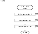
- FIG. 19 is a flowchart for describing noise removal processing when a ring buffer is configured using a memory in a column AD circuit by the image sensor of FIG. 18.
- FIG. It is a figure explaining the modification in a column AD circuit. It is a figure explaining the example of the arithmetic circuit realizable by the column AD circuit of FIG. It is a figure explaining the arithmetic processing implement
- FIG. 21 is a diagram illustrating a configuration example in the case of connecting a horizontal transfer line in the column AD circuit of FIG. 20. It is a block diagram which shows the structural example of the imaging device as an electronic device to which the camera module of this indication is applied. It is a figure explaining the usage example of the camera module to which the technique of this indication is applied.
- Non-Patent Document 2 a technique has been proposed in which a technique called a background difference method for detecting an object region by taking a difference between a background image and an input image is realized in an image sensor.
- a technique called a background difference method for detecting an object region by taking a difference between a background image and an input image is realized in an image sensor.
- the configuration of the memory for storing the background image is essential, the device configuration becomes large, and every time the input image is supplied, the background image is read out to be updated, and the updated background image Is overwritten, the operation becomes complicated and the apparatus configuration becomes complicated.
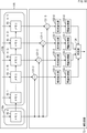
- the image sensor 1 described above includes, for example, an AD (Analog / Digital) conversion unit 11, an image reduction unit 12, a digital frame memory 13, a background update algorithm processing unit 14, a subtraction, as shown in FIG.
- the unit 15, the absolute value conversion unit 16, and the threshold processing unit 17 are configured.
- the AD conversion unit 11 converts a pixel signal composed of an analog signal supplied from a pixel array (not shown) into a digital signal and outputs the digital signal to the image reduction unit 12.
- the image reduction unit 12 reduces the image so as to reduce the resolution of the pixel signal converted into the digital signal, stores the image in the digital frame memory 13, and outputs it to the subtraction unit 15.
- the digital frame memory 13 stores the reduced image signal supplied from the image reduction unit 12, supplies the reduced image signal to the background update algorithm processing unit 14, and overwrites the processing result of the background update algorithm processing unit 14. .
- the background update algorithm processing unit 14 updates the background image using the reduced image that is the input image supplied from the image reducing unit 12 and writes it back to the digital frame memory 13. That is, the background image is sequentially updated and held in the digital frame memory 13 by this processing.
- the subtraction unit 15 obtains a difference between the reduced image supplied from the image reduction unit 12 and the background image stored in the digital frame memory 13 and subjected to the background update algorithm processing by the background update algorithm processing unit 14.
- the foreground image is supplied to the absolute value converting unit 16.
- the absolute value converting unit 16 determines the absolute value of the difference value between the reduced image that is the input image and the background image, and configures the difference image.
- the threshold processing unit 17 is composed of a moving image by binarization processing in which the pixel value of pixels larger than the threshold is set to 1 and the other pixels are set to 0 by comparing the difference value val and the threshold th in the difference image. Estimate the foreground area.
- the AD converter 11 converts an analog image signal into a digital signal.
- the image reduction unit 12 reduces the resolution of the image signal converted into the digital signal and stores it in the digital frame memory 13.
- the background update algorithm processing unit 14 repeats the process of updating and writing back the background image using the image signals sequentially stored in the digital frame memory 13.
- the subtraction unit 15 obtains a difference between the reduced image and the background image stored in the digital frame memory 13 and outputs the difference to the absolute value conversion unit 16.
- the absolute value conversion unit 16 supplies a difference image including a difference absolute value between the reduced image as the input image and the background image read from the digital frame memory 13 to the threshold processing unit 17.
- the threshold value processing unit 17 compares the pixel value val of each pixel of this difference image with the threshold value th to obtain a binary image in which the pixel value of a large pixel is 1 and the pixel values of other pixels are 0. As a result, an image for estimating the foreground area composed of the moving image is output.
- the digital frame memory 13 is indispensable for sequentially updating the background image, and thus the apparatus becomes large.
- the background update algorithm processing unit 14 needs to read the reduced image stored in the digital frame memory 13, update the background image, and then write it back to the digital frame memory 13, which increases power consumption. End up.
- the weighted averaging unit 41 assigns a large weight to the input image, which is the image processed by the weighted averaging unit 41 stored so far in the digital frame memory 13 and the reduced image that is the input image. By performing weighted averaging as described above, noise is removed from the image and output. Further, the weighted averaging unit 41 stores the weighted averaged image in the digital frame memory 13 and repeats the same processing to gradually remove noise.
- the weighted averaging unit 41 reads the image that is the previous processing result from the digital frame memory 13, performs the weighted averaging process using the input image, and writes it again in the digital frame memory 13. It is necessary to return, and power consumption becomes large. Further, since the digital frame memory 13 is an essential configuration, it is necessary to secure an installation area, and the apparatus becomes large.
- the imaging device has a function of generating pixel signals using all column AD circuits provided for each column for all pixels when imaging with high resolution.
- the imaging device of the present disclosure is not intended to capture an image. For example, when functioning as a sensor that detects each region of a background image and a foreground image, the resolution is reduced. Using the processed image, other arithmetic processing is executed using a column AD circuit that is not used for image processing caused by lowering the resolution. By realizing such an operation, a function for capturing a high-resolution image and a function as a sensor can be switched without adding a new configuration to the configuration of the image sensor.
- FIG. 3 shows a configuration example of the imaging device of the present disclosure.
- 3 includes a pixel array 71 having pixels arranged in two dimensions of m rows ⁇ n columns, and column AD circuits 72-0 to 72- (provided for each of n columns of vertical transfer lines. n-1) and an arithmetic circuit 73.
- column AD circuits 72-0 to 72- n-1
- the pixel array 71 has a photodiode for each pixel, generates a pixel signal corresponding to the amount of incident light, and supplies it to the column AD circuit 72 of each column via a vertical transfer line.
- a column AD (Analog Digital) circuit 72 converts a pixel signal composed of an analog signal supplied via a vertical transfer line into a digital signal and supplies the digital signal to the arithmetic circuit 73.
- the arithmetic circuit 73 performs various arithmetic processes on the pixel signal composed of digital signals supplied from the column AD circuits 72-0 to 72- (n-1), and outputs an arithmetic result.
- the pixel array 71 captures a high-resolution image signal using all the pixels, and further operates differently depending on the operation mode.
- the operation modes include an image capturing mode for capturing a high resolution image using all pixels and a sensor mode using information on a low resolution image. For example, in the sensor mode, a difference image that identifies a foreground region in which a foreground image made up of moving images in the image is captured and a background region in which a background image is captured is output.
- the pixel array 71 generates a low-resolution image with respect to the resolution of all pixels by pixel addition or thinning, and sends the low-resolution pixel signal to the corresponding column AD circuit 72.
- FIG. 3 shows a configuration when a low-resolution image of p pixels composed of a predetermined number of pixel groups 71a-1 to 71a-p among the pixels constituting the pixel array 71 is captured.
- a column AD circuit 72 that is not used for image processing is generated due to the use of a low-resolution image. Therefore, a difference is obtained by using the column AD circuit 72 that is not used for image processing. Arithmetic processing other than imaging processing, such as generating an image, is executed.
- a pixel signal that treats the pixel array 71 as a single pixel group 71a-1 composed of a predetermined number of pixels is supplied to the column AD circuits 72-0 to 72-. 2 and the pixel signal that treats the pixel group 71a-2 as one pixel is processed by the column AD circuits 72-3 to 72-5.
- a pixel signal that treats the pixel group 71a- (p-1) as one pixel is processed by the column AD circuits 72- (n-6) to 72- (n-4), and the pixel group 71a-p is treated as one pixel.
- the column AD circuits 72-0 to 72-n include calculators 72a-0 to 72a-n, respectively, but sequentially shift the calculation results to adjacent column AD circuits 72 in units of one frame.
- a pixel signal of the 0th frame is supplied to the column AD circuit 72-0 as a pixel signal with the pixel group 71a-1 as one pixel, and a pixel signal with the pixel group 71a-2 as one pixel is The pixel signal supplied to the column AD circuit 72-3,... With the pixel group 71a- (p-1) as one pixel is supplied to the column AD circuit 72- (n-6), and the pixel group 71a-p Is supplied to the column AD circuit 72- (n-3), the pixel signal is converted from an analog signal to a digital signal and held.
- the column AD circuits 72-0, 72-3,... 72- (n-6), 72- (n-3) are held respectively. Are shifted to the column AD circuits 72-1, 72-4,... 72- (n-5), 72- (n-2) on the right side.
- a pixel signal for the pixel group 71a-1 as one pixel is supplied to the column AD circuit 72-0, and a pixel group 71a-2 as one pixel.
- the pixel signal is supplied to the column AD circuit 72-3,...,
- the pixel signal having the pixel group 71a- (p-1) as one pixel is supplied to the column AD circuit 72- (n-6)
- a pixel signal having the group 71a-p as one pixel is supplied to the column AD circuit 72- (n-3).
- the column AD circuit 72 converts a pixel signal constituting an image from an analog signal to a digital signal in units of rows and outputs the converted signal.
- the pixel group 71a in the sensor mode, is regarded as one pixel, so that a low-resolution image is configured and a memory including a latch circuit included in the plurality of column AD circuits 72 and the like.
- a plurality of frames of the low-resolution image are stored in place of the frame memory and used for buffering and computation.
- the pixel value of each pixel constituting the pixel group 71a may be added to obtain an average, or any of the representative pixels The pixel value may be used, or the median of the pixel values of the pixels constituting the pixel group 71a may be used.
- FIG. 3 shows an example in which a low-resolution image signal is accumulated for three frames by repeating the same processing. Then, when a new low resolution pixel signal for one frame is supplied, the oldest pixel signal is discarded and the latest three frames of pixel signals are accumulated.
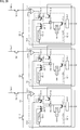
- each of the column AD circuits 72 includes an arithmetic unit 72a. More specifically, the arithmetic unit 72a includes, for example, a comparator 91, a combinational circuit 92, and The memory 93 is used.
- the column AD circuits 72-0 to 72-2 include comparators 91-0 to 91-2, combinational circuits 92-0 to 92-2, and a memory 93-, respectively. 0 to 93-2.
- the comparator 91 compares the pixel signal supplied from the vertical transfer line with the reference voltage, and supplies the comparison result to the combinational circuit 92.
- the combinational circuits 92-0 to 92-2 realize AD conversion processing in the image capturing mode. In the sensor mode, various circuits combined to function as an AD circuit are appropriately used. Used to perform various operations and supply them to the memories 93-0 to 93-2.
- the memories 93-0 to 93-2 are composed of, for example, a latch circuit, and temporarily store calculation results.
- the combinational circuits 92-0 to 92-2 include, for example, selectors 101-0 to 101-2, 102-0 to 102-2, sign inversion units 103-0 to 103-2, and selectors 104-0 to 104-2, respectively. , Adders 105-0 to 105-2, absolute value conversion units 106-0 to 106-2, and selectors 107-0 to 107-2.
- the selectors 101 and 102, the sign inversion unit 103, the selector 104, the adder 105, the absolute value conversion unit 106, and the selector 107 of the combinational circuit 92 are a so-called counter or the like together with the comparator 91 and the memory 93 in the image capturing mode. It realizes equivalent functions and realizes AD conversion.
- the selectors 101 and 102, the sign inverting unit 103, the selector 104, the adder 105, the absolute value converting unit 106, and the selector 107 of the combinational circuit 92 are adjacent to the column AD circuit on the left side in the drawing.
- the selector 101 outputs 0 or 1 based on the comparison result of the comparator 91 and supplies it to the selector 102.
- the selector 102 selectively outputs either the value in the memory 93 of the column AD circuit 72 on the left side or the value supplied from the selector 101 to the adder 105.
- the sign inversion unit 103 inverts the sign of the value stored in the memory 93 and supplies it to the selector 104.
- the selector 104 selectively outputs the value of its own memory 93, the value of its own memory 93 from the sign inverting unit 103, the sign of which is inverted, or 0 to the adder 105.
- Adder 105 adds the value output from selector 102 and the value output from selector 104 and outputs the result to absolute value converting section 106 and selector 107.
- the absolute value converting unit 106 obtains the absolute value of the value supplied from the adder 105 and supplies it to the selector 107.
- the selector 107 selectively stores either the value supplied from the adder 105 or the value supplied from the absolute value conversion unit 101 in the memory 93.
- the column AD circuit 72 transfers the value stored in the AD conversion circuit or the memory 93 of the column AD 72 on the left side, or is stored in the memory 93 with the transferred value. It functions as an arithmetic circuit that adds a certain value.
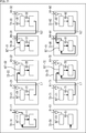
- the selector 101 when functioning as an AD conversion circuit, the selector 101 as shown in the left part of FIG. 5 based on the comparison result of the comparator 91 as shown by the thick lines in the left part and the right part of FIG. 1 selectively outputs 1 or the selector 101 selectively outputs 0 as shown in the right part of FIG. Then, the selector 102 supplies the output value of the selector 101 to the adder 105.
- the selector 104 reads out the value stored in the memory 93 and outputs it to the adder 105.
- the adder 105 adds the values supplied from the selectors 102 and 104, respectively, and outputs the result to the selector 107 and the absolute value converting unit 106.
- the selector 107 stores the value output from the adder 105 in the memory 93. Thereafter, the same processing is repeated.
- the adder 105 supplies the value of the memory 93 of the column AD circuit 72 on the left side to the absolute value conversion unit 106 and the selector 107 substantially.
- the selector 107 stores the value stored in the memory 93 of the left column AD circuit 72 supplied from the adder 105 in its own memory 93.
- the selector 102 selects the value of the memory 93 of the column AD circuit 72 on the left side and supplies it to the adder 105, and the sign inversion unit 103 is stored in its own memory 93.
- the selector 104 inverts the sign of the existing value, and supplies the adder 105 with the value whose sign has been inverted by the sign inversion unit 103.
- the adder 105 adds the value of the memory 93 of the column AD circuit 72 on the left to the value stored in its own memory 93 and supplies the sum to the absolute value conversion unit 106 and the selector 107.
- the absolute value converting unit 106 obtains the absolute value of the addition result by the adder 105 and supplies it to the selector 107.
- the selector 107 writes the addition result supplied from the absolute value converting unit 106 back into its own memory 93 and stores it.
- each combinational circuit 92 in the column AD circuit 72 performs AD conversion processing, calculates and outputs the absolute difference value of the sequentially supplied pixel values, and stores it in the memory 93.
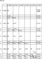
- step S11 the combinational circuit 92-0 of the column AD circuit 72-0 supplies the 0th frame supplied via the vertical transfer line.
- the pixel signal is AD converted and stored in the memory 93-0 as a pixel value val0 composed of a digital signal.
- step S12 as shown in the middle left portion of FIG. 7, the combinational circuit 92-1 of the column AD circuit 72-1 is connected to the memory of the column AD circuit 72-0 adjacent to the left side via the wiring L-0.
- the pixel value val0 is read from 93-0 and stored in the memory 93-1. This operation corresponds to the operation on the left side of FIG. 6 described above.
- step S13 as shown in the lower left part of FIG. 7, the combinational circuit 92-0 of the column AD circuit 72-0 AD-converts the pixel signal of the first frame supplied via the vertical transfer line. Then, it is stored in the memory 93-0 as a pixel value val1 composed of a digital signal.
- step S14 as shown in the upper right part of FIG. 7, the combinational circuit 92-1 of the column AD circuit 72-1 is connected to the memory of the column AD circuit 72-0 adjacent to the left side via the wiring L-0.
- ) is written back to the memory 93-1.
- This operation corresponds to the operation on the right side of FIG. 6 described above.
- step S15 as shown in the middle right part of FIG. 7, the calculation result ad01, which is the absolute difference value stored in the memory 93-1, is output as the interframe difference calculation result.
- step S16 as shown in the lower right part of FIG. 7, the combinational circuit 92-1 of the column AD circuit 72-1 is connected to the memory of the column AD circuit 72-0 adjacent to the left side via the wiring L-0.
- the pixel value val1 is read from 93-0 and stored in the memory 93-1. That is, the pixel value val1 is shifted by one column. This operation corresponds to the operation on the left side of FIG. 6 described above.
- step S13 when pixel signals are sequentially supplied, the processing after step S13 is sequentially repeated, and an image composed of pixel signals of inter-frame differences is sequentially output.
- the inter-frame difference image without newly adding the configuration of the image sensor while the image is a low-resolution image with respect to the resolution of the pixel array 71, for example, a moving image region with a low resolution It is possible to generate a difference image that distinguishes a foreground region that is not a moving image, that is, a background region that does not move. Also, until the intruder is detected as a foreground area in a monitoring image or the like by detecting the foreground area that is a moving image area, the sensor operates in the sensor mode, and only when the intruder is detected, the image capturing mode is set. It is possible to switch and capture a high-resolution image.
- the apparatus configuration can be reduced in size.
- Ring buffer In the above description, the example in which the inter-frame difference is sequentially obtained using the pixel signal whose resolution has been reduced has been described. However, the pixel signal is sequentially stored in the memory 93 in the column AD circuit 72, and the pixel signal of the next frame is further stored.
- a ring buffer between a plurality of frames may be configured by performing a process of only shifting to an adjacent column AD circuit 72 each time.
- the basic operation can be realized by simply repeating the operation of shifting the pixel signal to the adjacent column AD circuit 72 without executing the above-described difference calculation.
- the pixel signal “1” of the frame F1 which is the first frame, is AD-converted by the column AD circuit 72-0 and stored in the memory 93-0.
- the pixel signal “1” stored in the memory 93-0 is adjacent to the adjacent column AD as shown in the upper center of FIG.
- the pixel signal “2” of the new frame F2 is stored in the memory 93-0 of the column AD circuit 72-0 while being shifted to the memory 93-1 of the circuit 72-1.
- the column AD circuit in which the pixel signal “1” stored in the memory 93-1 is adjacent is shown.
- the pixel signal “2” that has been shifted to the memory 93-2 of 72-2 and stored in the memory 93-0 is shifted to the memory 93-1 of the adjacent column AD circuit 72-1.
- the pixel signal “3” of the new frame F3 is stored in the memory 93-0 of the column AD circuit 72-0.
- a pixel signal is sequentially supplied for each frame, it is sequentially shifted to the memory 93 of the column AD circuit 72 adjacent in the right direction in the figure, and the pixel signal of the oldest frame is discarded.
- the pixel signals for the latest three frames are always accumulated, and as a result, a ring buffer can be realized.
- the pixel signal “1” of the frame F1 which is the first frame, is AD-converted by the column AD circuit 72-0 and stored in the memory 93-0.
- the pixel signal “1” stored in the memory 93-0 is adjacent to the adjacent column AD as shown in the upper center of FIG.
- the pixel signal “2” of the new frame F2 is stored in the memory 93-0 of the column AD circuit 72-0 while being shifted to the memory 93-1 of the circuit 72-1.
- the column AD circuit to which the pixel signal “1” stored in the memory 93-1 is adjacent as shown in the lower left part of FIG.
- the pixel signal “3” that has been shifted to the memory 93-2 of the 72-2 and stored in the memory 93-0 is shifted to the memory 93-1 of the adjacent column AD circuit 72-1.
- the pixel signal “4” of the new frame F4 is overwritten and stored in the memory 93-0 of the column AD circuit 72-0.
- the pixel signal “4” stored in the memory 93-0 is discarded as shown in the lower center part of FIG.
- the pixel signal “5” of the correct frame F5 is stored in the memory 93-0 of the column AD circuit 72-0.
- the pixel signal “5” stored in the memory 93-0 is discarded as shown in the lower right part of FIG. Is overwritten by the pixel signal “6” of the new frame F6 and stored in the memory 93-0 of the column AD circuit 72-0.
- the pixel signals of the oldest frame are shifted to the memory 93 of the column AD circuit 72 adjacent in the right direction in the figure every N frames (every other frame). Discarded, the pixel signals for the latest three frames are always accumulated every other frame, and as a result, a ring buffer can be realized.
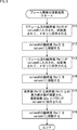
- step S31 a counter n is initialized to 1 by a control unit (not shown).
- step S32 a control unit (not shown) determines whether a pixel signal of a new frame has been supplied, and the same processing is repeated until it is transmitted.
- step S32 when a pixel signal of a new frame has been supplied, the process proceeds to step S33.
- step S34 the combinational circuit 92-0 AD-converts the pixel signal and discards the pixel signal stored until the AD conversion is performed in the memory 93-0. Advances to step S35. In the first process, since there is no value, it is stored as it is.
- step S35 the counter n (not shown) increments the counter n by 1, and the process returns to step S32.
- step S33 when the counter n becomes N + 1, a process progresses to step S36.
- step S36 the combinational circuit 92-1 reads out the pixel signal from the memory 93-0 of the column AD circuit 72-0 adjacent on the left side in FIG. 4 and stores it in the memory 93-1, thereby storing the pixel signal in one column. Shift by minutes.
- step S37 the combinational circuit 92-0 AD-converts the pixel signal and stores it in the memory 93-0, and the process proceeds to step S38.
- step S38 the combinational circuit 92-0 determines whether or not the process is finished. If the process is not finished, the process returns to step S31 and the subsequent processes are repeated. Then, when it is determined in step S38 that the process is to be terminated, the process is terminated.
- the pixel signal is sequentially shifted to the memory 93 of the column AD circuit 72 on the right side every arbitrary N frames, and a ring buffer can be configured.
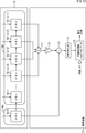
- FIG. 12 shows a configuration example of the arithmetic circuit 73 that calculates the background image using the ring buffer including the memory 93 described above.
- the memory 93-0 has a buffer 110a for storing the pixel signal of the latest frame, and a buffer comprising the memories 93-1 to 93- (n-1) for storing the pixel signals of the past frame. 110b, and the buffers 110a and 110b constitute a ring buffer 110.
- the 12 includes an adding unit 111, a gain amplifier 112, a subtracting unit 113, an absolute value converting unit 114, and a threshold processing unit 115.
- the adder 111 holds, from among the memories 93-0 to 93-N constituting the ring buffer 110, the memory 93- (n ⁇ 1) to 93- (n-4) pixel signals are added and supplied to the gain amplifier 112.
- the gain amplifier 112 holds the pixel signal of the oldest frame from the pixel signal of the oldest frame among the memories 93-0 to 93-N constituting the ring buffer 110, and holds the pixel signal of the oldest frame 93- (n ⁇ 1). ) To 93- (n ⁇ 4) are added to the gain of 1 ⁇ 4 to obtain an average value of the pixel signals and output the result to the subtractor 113.
- the subtracting unit 113 averages the pixel signal of the memory 93-0 in which the pixel signal of the newest frame is held and the pixel signal of the oldest frame from the oldest frame pixel signal supplied from the gain amplifier 112 to the fourth oldest frame. Is obtained and supplied to the absolute value conversion unit 114.
- the absolute value converting unit 114 obtains the absolute value of the pixel value that is the difference output from the subtracting unit 113 as the difference absolute value, and outputs the absolute value to the threshold processing unit 115.
- the threshold processing unit 115 compares the pixel value val, which is the difference absolute value supplied from the absolute value converting unit 114, with the predetermined threshold th and sets the pixel value of a pixel larger than the predetermined threshold th to 1, A binarized difference image in which the pixel values of the other pixels are 0 is output. From the binarized difference image, an image including a foreground region having a pixel value “1” and a background region having a pixel value “0” is generated, and the foreground region and the background region are estimated. It becomes possible to do.
- the pixel values 0 and 1 may be interchanged, or may be expressed by other binary values.
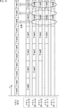
- the pixel signal of frame 0 (frame 0) is stored in the ring buffer 110 formed by the memories 93-1 to 93- (n-1), and the frame 0 (frame 0) is stored in the memory 93- (n-5). Is stored at the timing of supply, and frame 1 (frame 1) is skipped. Then, at the timing of frame 2 (frame 2), the pixel signal of frame 0 (frame 0) is shifted to the memory 93- (n-4) and at the same time, the frame 93 (frame 2) Is supplied and stored, and this state is maintained even at the timing of frame 3 (frame 3).
- the pixel signal of frame 0 (frame 0) is shifted to the memory 93- (n-3), and the pixel signal of frame 2 (frame 2) is shifted to the memory 93- (n -4), the frame 4 (frame 4) is supplied and stored in the memory 93- (n-5), and this state is maintained even at the timing of the frame 5 (frame 5).
- the pixel signal of frame 0 (frame 0) is shifted to the memory 93- (n-2), and the pixel signal of frame 2 (frame 2) is shifted to the memory 93- (n -3), the pixel signal of frame 4 (frame4) is shifted to the memory 93- (n-4), and the frame 6 (frame6) is supplied to the memory 93- (n-5).
- This state is also maintained at the timing of frame 7 (frame 7).
- the pixel signal of frame 0 (frame 0) is shifted to the memory 93- (n-1), and the pixel signal of frame 2 (frame 2) is shifted to the memory 93- (n -2), the pixel signal of frame 4 (frame4) is shifted to the memory 93- (n-3), and the pixel signal of frame 6 (frame6) is transferred to the memory 93- (n-3).
- the frame 8 (frame 8) is supplied and stored in the memory 93- (n-5), and this state is maintained even at the timing of the frame 9 (frame 9).
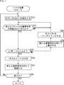
- background difference calculation processing Next, background difference calculation processing by the calculation circuit 73 of FIG. 12 will be described with reference to the flowchart of FIG. Here, it is assumed that an average value of pixel signals for four frames is obtained from the oldest one.
- step S51 the gain amplifiers 111-0 to 111-3 respectively select the pixels of the oldest frame from the pixel signal of the oldest frame to the Nth of the memories 93-0 to 93- (n-1) constituting the ring buffer.
- the pixel signals of the memories 93- (n-1) to 93- (n-4) holding the signals are read out.
- step S52 the adder 111 adds the pixel signals of the oldest frame pixel from the oldest frame pixel signal held in the ring buffer 110, and supplies the result to the gain amplifier 112.
- step S53 the gain amplifier 112 sets the gain of the added pixel signal to 1 ⁇ 4, obtains the average value of the pixel signals of the oldest frame pixel from the oldest frame pixel signal, and supplies the average value to the subtractor 113.
- step S54 the subtractor 113 subtracts the pixels of the oldest frame from the pixel signal of the memory 93-0 in which the pixel signal of the newest frame is held and the pixel signal of the oldest frame supplied from the adder 112. A difference from the average value of the signal is obtained and supplied to the absolute value converting unit 114.
- step S55 the absolute value converting unit 114 obtains the absolute value of the pixel value that is the difference output from the subtracting unit 113, and outputs the absolute value to the threshold processing unit 115 as the difference absolute value.
- step S56 the threshold processing unit 115 compares the pixel value val, which is the difference absolute value supplied from the absolute value converting unit 114, with the predetermined threshold th and the pixel value of the pixel larger than the predetermined threshold th. 1 is output, and a binary difference image with the pixel values of the other pixels being 0 is output.
- the foreground area and the background area can be estimated from the binarized difference image.
- the foreground region and the background region are estimated using the absolute difference between the average value of the oldest four frames and the pixel signal of the latest frame among the pixel signals stored in the ring buffer 110.
- the average value of the oldest plurality of frames the average value of the number of frames other than 4 frames may be obtained.
- the ring buffer 110 using the memories 93-0 to 93- (n-1) uses the absolute value of the difference between the pixel signal in the latest frame and the average value of the pixel signals for the four oldest frames.
- the pixels with the absolute difference when the absolute difference between the pixel signal in the latest frame and each of the four oldest frames is larger than the threshold are regarded as the foreground region, and the other pixels It may be regarded as a background area.
- FIG. 16 shows the case where the ring buffer 110 using the memories 93-0 to 93- (n-1) has all the absolute differences between the pixel signal in the latest frame and the four oldest frames larger than the threshold value.
- This is a first application example of the arithmetic circuit 73 in which only the pixels having the difference absolute value are regarded as the foreground region and the other pixels are regarded as the background region.
- 16 includes subtracters 131-0 to 131-3, absolute value conversion units 132-0 to 132-3, threshold value processing units 133-0 to 133-3, and a determination unit 134.
- the subtracters 131-0 to 131-3 read out the oldest four frames of pixel signals stored in the memories 93-N to 93- (N-3), and update the latest signals stored in the memory 93-0.
- the difference from the pixel signal of the input image is obtained and supplied to the absolute value converting sections 132-0 to 132-3, respectively.
- the absolute value conversion units 132-0 to 132-3 supply the supplied difference values to the threshold value processing units 133-0 to 133-3 as absolute difference values.
- Each of the threshold processing units 133-0 to 133-3 compares the difference absolute value with a predetermined threshold, sets the pixel value to 1 for pixels larger than the threshold, and sets the pixel value to 0 for other pixels.
- a converted image is generated and supplied to the determination unit 134.
- the determination unit 134 sets the pixel value of only the pixels whose pixel values are 1 to 1 for each pixel of the four binarized images supplied from the threshold processing units 133-0 to 133-3, The pixel values of the other pixels are set to 0.
- step S71 the subtracters 131-0 to 131-3 have the four oldest pixel signals (N pixel signals) stored in the memories 93- (n-1) to 93- (n-4). ).
- step S72 the subtracters 131-0 to 131-3 obtain the difference between the pixel signals for the four oldest read frames and the pixel signal of the latest input image stored in the memory 93-0. Are supplied to the absolute value converting sections 132-0 to 132-3, respectively.
- step S73 the absolute value converting units 132-0 to 132-3 obtain absolute values of the supplied difference values, and supply them to the threshold processing units 133-0 to 133-3 as the absolute difference values.
- each of the threshold processing units 133-0 to 133-3 compares the absolute difference value with a predetermined threshold, sets the pixel value to 1 for pixels larger than the threshold, and sets the pixel value to 0 for other pixels. Is generated and supplied to the determination unit 134.
- step S75 the determination unit 134 calculates pixel values of only pixels whose pixel values are all 1 for each pixel of the four binarized images supplied from the threshold processing units 133-0 to 133-3. 1 and the pixel values of the other pixels are 0.
- a range in which leaves are included in the background and the area is not stably regarded as the foreground area due to fluctuations in the wind, for example, is reliably regarded as the background area, and the subject has moved stably. Only the range can be regarded as the foreground region.
- the ring buffer 110 using the memories 93-0 to 93- (n-1) uses the ring buffer 110 to compare the absolute value of the difference between the pixel signal in the latest frame and the oldest four frame pixel signals.
- noise removal may be realized by obtaining an average of pixel signals in all frames stored in the ring buffer 110.
- FIG. 18 shows an operation of the arithmetic circuit 73 that realizes noise removal by obtaining an average of pixel signals in all frames by the ring buffer 110 using the memories 93-0 to 93- (n-1). A configuration example is shown.
- the 18 includes an adder 151 and a gain amplifier 152.
- the adder 151 adds the pixel signals of all frames for n frames stored in the memories 93-0 to 93-(n ⁇ 1) and supplies the result to the gain amplifier 152.
- the gain amplifier 152 includes a gain amplifier 152 that obtains an average value in the ring buffer by multiplying the addition result of the adder 151 by a gain of 1 / n.
- step S91 the adder 151 reads out and adds all the n-frame pixel signals stored in the memories 93-0 to 93- (n-1), and supplies the addition result to the gain amplifier 152.
- step S92 the gain amplifier 152 multiplies the addition result by a gain of 1 / n to obtain an average value of the pixel signals.
- step S93 the gain amplifier 152 outputs an average value for all frames of the pixel signal.
- a horizontal transfer line 191 for connecting the vertical transfer lines 192 is provided, and switches 181-0 to 181-2 for switching on or off the connection between the vertical transfer lines 192 are provided. Yes.
- switches 182-0 to 182-2 for switching on / off the connection of the vertical transfer line are provided.
- the value of the memory 93 provided between the column AD circuits 72-0 and 72-1 and between the column AD circuits 72-1 and 72-2 is transferred to the adjacent left column AD circuit 72.
- wirings L2-1 and L2-2 for transferring to the right column AD circuit 72 are provided.
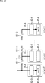
- FIG. 20 is different from FIG. 4 in that a combinational circuit 92 ′ is provided instead of the combinational circuit 92.
- the combinational circuit 92 ′ has the same basic function as the combinational circuit 92, but differs in that a selector 171 is further provided.
- the selector 171 selects either the pixel signal of the memory 93 of the column AD circuit 72 on the right side or 0 from the right according to the operation mode, and supplies the selected signal to the adder 105. Therefore, in the combinational circuit 92 ′ in FIG. 20, the adder 105 adds the three values supplied from the selectors 102, 104, and 171 and supplies the sum to the absolute value conversion unit 106 and the selector 107.
- the comparator 91-11 compares the pixel signal of the analog signal supplied from the vertical transfer line with the reference.
- the combinational circuit 92′-11 is supplied to the combinational circuit 92′-11 so that the combinational circuit 92′-11 can function as a count-up circuit or a count-down circuit used for AD conversion.
- the thick line on each wiring indicates the movement path of the pixel signal.
- the combination circuit 92′-22 of the column AD circuit 72-22 is connected to the column AD on the left side via the wiring L1.
- the pixel signal stored in the memory 93-21 of the circuit 72-21 is read out and stored in the memory 93-22, whereby the pixel signal stored in the memory 93-21 of the column AD circuit 72-21 is It becomes possible to function as a right shift processing circuit to be moved to the memory 93-22 of the column AD circuit 72-22.
- the combination circuit 92′-31 of the column AD circuit 72-31 is connected to the column AD on the right side via the wiring L2.
- the pixel signal stored in the memory 93-32 of the circuit 72-32 is read out and stored in the memory 93-31, whereby the pixel signal stored in the memory 93-32 of the column AD circuit 72-32 is It becomes possible to function as a left shift processing circuit to be moved to the memory 93-31 of the column AD circuit 72-31.
- the initial value is set by storing the pixel signal as the initial value in the memory 93-51 of the column AD circuit 72-51, as shown by the column AD circuit 72-51. It becomes possible to function as a circuit.
- the combinational circuit 92′-72 of the column AD circuit 72-72 is connected via the wiring L1.
- Functions as a right shift operation circuit that reads out the pixel signal stored in the memory 93-71 of the column AD circuit 72-71 on the left, calculates the value together with the value stored in the memory 93-72, and stores it in the memory 93-72 It becomes possible to make it.
- the combinational circuit 92′-91 of the column AD circuit 72-91 is connected via the wiring L2.
- the pixel signal stored in the memory 93-92 of the column AD circuit 72-92 on the left is read, calculated using the value stored in the memory 93-91, and stored in the memory 93-91 to shift left It can function as an arithmetic circuit.
- column AD circuits 72-0 to 72-5 are provided for 6 columns from the 0th column (column0) to the 5th column (column5), and the column AD circuits 72-0 and 72-4 are used for AD conversion.
- the column AD circuits 72-1 to 72-3 function as right shift processing circuits
- the column AD circuit 72-5 functions as an initial value setting circuit
- the column AD circuit 72-4 Furthermore, by making it function as a right shift arithmetic circuit as shown in FIG. 5, it becomes possible to realize the processing as shown in FIG.
- the column AD circuit 72-5 of column 5 functions in advance as an initial setting circuit, and a threshold value (thresh) is set in the memory 93-5.
- the combinational circuit 92′-0 of the column AD circuit 72-0 performs AD conversion.
- the data is stored in the memory 93-0 in the column AD circuit 72-0 (column0).
- the combinational circuit 92'-1 of the column AD circuit 72-1 shifts the pixel value (val0) stored in the memory 93-0 in column0 to the memory 93-1 in column1.
- the pixel value (val0) is shifted from the memory 93-1 in the column 1 to the memory 93-2 in the column 2, and similarly, the pixel value (val1) is changed from the memory 93-0 in the column 0 to the memory 93- in the column 1. Shifted to 1.
- AD conversion is sequentially performed on the pixel value (val2) of the second frame (frame2), and is stored in the memory 93-0 of column0 at timing T8.
- the pixel value (val0) of column2 is shifted to the memory 93-3 of column3, the pixel value (val1) of column1 is shifted to the memory 93-2 of column2, and the pixel value (val2) of column0 is changed. Shifted to memory 93-1 in column1.
- the pixel values val0 to val3 of the column 0 to 3 are shifted to the memories 93-3 to 93-1 of the column AD circuits 72-3 to 72-1 adjacent to the right side, respectively.
- the combinational circuit 92-4 causes the pixel value (val0) stored in the memory 93-3 of the column 3 column AD circuit 72-3 and the column 4 column AD.
- the absolute value of the difference is obtained by calculation with the pixel value (val3) AD-converted by the circuit 72-4, and the calculation result (abs_diff03) is stored in the memory 93-4 of the column AD circuit 72-4 of column4.
- the threshold value (thresh) set in the column AD circuit 72-5 of column5 is shifted to the column AD circuit 72-4 of column4, and is subtracted from the difference absolute value (abs_diff03), and the subtraction result (diff03) Save.
- this pixel is regarded as a foreground region including a moving object.
- Such an operation makes it possible to construct a differential image composed of a binary image composed of a foreground region and a background region.
- the imaging device of the present disclosure it is not necessary to add a digital frame memory by performing arithmetic processing using the memory 93 in the column AD circuit 72, so that the mounting area can be reduced accordingly. Therefore, it is possible to reduce the size of the apparatus. In addition, since there is no need to provide a digital frame memory, it is possible to reduce the leakage current and to realize power saving.
- the pixel can be made smaller than the method having a memory in the pixel, it is possible to realize a larger number of pixels or a smaller area.
- the above-described imaging element 51 can be applied to various electronic devices such as an imaging device such as a digital still camera or a digital video camera, a mobile phone having an imaging function, or other devices having an imaging function. .
- FIG. 24 is a block diagram illustrating a configuration example of an imaging device as an electronic apparatus to which the present technology is applied.
- An imaging apparatus 501 shown in FIG. 24 includes an optical system 502, a shutter apparatus 503, a solid-state imaging element 504, a driving circuit 505, a signal processing circuit 506, a monitor 507, and a memory 508.
- the imaging apparatus 501 shown in FIG. Imaging is possible.
- the optical system 502 includes one or a plurality of lenses, guides light (incident light) from the subject to the solid-state image sensor 504, and forms an image on the light-receiving surface of the solid-state image sensor 504.
- the shutter device 503 is disposed between the optical system 502 and the solid-state imaging device 504, and controls the light irradiation period and the light-shielding period to the solid-state imaging device 504 according to the control of the drive circuit 1005.
- the solid-state image sensor 504 is configured by a package including the above-described solid-state image sensor.
- the solid-state imaging device 504 accumulates signal charges for a certain period in accordance with light imaged on the light receiving surface via the optical system 502 and the shutter device 503.
- the signal charge accumulated in the solid-state image sensor 504 is transferred according to a drive signal (timing signal) supplied from the drive circuit 505.
- the drive circuit 505 outputs a drive signal for controlling the transfer operation of the solid-state image sensor 504 and the shutter operation of the shutter device 503 to drive the solid-state image sensor 504 and the shutter device 503.
- the signal processing circuit 506 performs various types of signal processing on the signal charges output from the solid-state imaging device 504.
- An image (image data) obtained by the signal processing by the signal processing circuit 506 is supplied to the monitor 507 and displayed, or supplied to the memory 508 and stored (recorded).
- Imaging apparatus 501 configured as described above, a circuit configuration required for calculation is obtained by applying the imaging element 51 instead of the optical system 502, the shutter apparatus 503, and the solid-state imaging element 504 described above. Imaging can be performed by switching between the image capturing mode and the sensor mode without increasing the number, and the apparatus can be reduced in size and power can be saved.
- FIG. 25 is a diagram illustrating a usage example in which the above-described imaging element 51 is used.
- the camera module described above can be used in various cases for sensing light such as visible light, infrared light, ultraviolet light, and X-ray as follows.
- Devices for taking images for viewing such as digital cameras and mobile devices with camera functions
- Devices used for traffic such as in-vehicle sensors that capture the back, surroundings, and interiors of vehicles, surveillance cameras that monitor traveling vehicles and roads, and ranging sensors that measure distances between vehicles, etc.
- Equipment used for home appliances such as TVs, refrigerators, air conditioners, etc. to take pictures and operate the equipment according to the gestures ⁇ Endoscopes, equipment that performs blood vessel photography by receiving infrared light, etc.
- Equipment used for medical and health care ⁇ Security equipment such as security surveillance cameras and personal authentication cameras ⁇ Skin measuring instrument for photographing skin and scalp photography Such as a microscope to do beauty Equipment used for sports-Equipment used for sports such as action cameras and wearable cameras for sports applications-Used for agriculture such as cameras for monitoring the condition of fields and crops apparatus
- this indication can also take the following structures.
- a plurality of analog-digital converters provided for each column in which the plurality of pixels are arranged, and converting the pixel signal from an analog signal to a digital signal;
- a part of the plurality of analog-to-digital converters performs analog-to-digital conversion on a pixel signal constituting a low-resolution image having a resolution lower than that of the pixel array, and at least the part of the analog-to-digital converters
- An image sensor that performs arithmetic processing using pixel signals that form a resolution image.
- the analog-digital conversion unit includes a storage unit that stores a result of the arithmetic processing,
- the image sensor according to ⁇ 1> in which at least the analog-to-digital conversion unit other than the part stores pixel signals constituting a low-resolution image for a plurality of frames having different timings.
- At least the analog-to-digital conversion unit other than the part receives the pixel signal stored in the storage unit of the adjacent analog-to-digital conversion unit when a pixel signal of a new low-resolution image is supplied.
- the image pickup device according to ⁇ 2>, wherein pixel signals constituting low-resolution images for a plurality of frames having different timings are stored by reading and shifting to the storage unit.
- At least the analog-to-digital conversion unit other than the part is when a pixel signal of a new low-resolution image is supplied, and is stored in the storage unit for each predetermined number of frames.
- the pixel signals constituting the low-resolution images for a plurality of frames with different timings are stored by sequentially shifting the stored pixel signals to the storage unit of the analog-digital conversion unit adjacent to each other, and storing the pixel signals.
- Image sensor. ⁇ 5> Arithmetic processing for obtaining an inter-frame difference image of pixel signals constituting the low-resolution image for a plurality of frames having different timings stored in the storage unit, at least the analog-digital conversion unit other than the part.
- At least the analog-to-digital conversion unit other than the part reads out a pixel signal constituting the low-resolution image for one frame at a predetermined timing, which is stored in the storage unit, and creates a new frame pixel
- the image sensor according to ⁇ 5> wherein an inter-frame difference image with a signal is obtained and overwritten in the storage unit.
- the ring buffer is configured by storing pixel signals constituting low-resolution images of a predetermined number of a plurality of frames having different timings by shifting and storing the data in the storage unit of the conversion unit.
- a calculation unit that calculates a difference image between a pixel signal constituting the low-resolution image of a plurality of frames of a predetermined number of different timings stored in the ring buffer and a pixel signal of the new low-resolution image
- the calculation unit includes an average value in each pixel of pixel signals constituting the low-resolution image from the oldest frame stored in the ring buffer to a predetermined oldest frame, and the new low-resolution image.
- the absolute value of the difference from the pixel signal is calculated, a pixel having the absolute difference greater than a predetermined threshold is defined as a first pixel value, and a pixel having the absolute difference smaller than the predetermined threshold is defined as a second pixel value.
- the calculation unit includes a weighted average value corresponding to the timing of pixel signals constituting the low-resolution image from the oldest frame stored in the ring buffer to a predetermined oldest frame, and A difference absolute value with a pixel signal of a new low-resolution image is calculated, a pixel having the difference absolute value larger than a predetermined threshold is defined as a first pixel value, and a pixel having the difference absolute value smaller than the predetermined threshold is determined.
- the image sensor according to ⁇ 9> wherein a difference image including a binary image serving as a second pixel value is calculated.
- the calculation unit includes each of a pixel signal constituting the low-resolution image from the oldest frame stored in the ring buffer to a predetermined oldest frame, and a pixel signal of the new low-resolution image
- the difference absolute value of each of the difference absolute values is calculated, a pixel in which each of the difference absolute values is larger than a predetermined threshold is set as a first pixel value, and a pixel in which any of the difference absolute values is smaller than the predetermined threshold
- the image sensor according to ⁇ 9> wherein a difference image including a binary image serving as a second pixel value is calculated.
- the imaging apparatus further including a calculation unit that calculates an average value of pixel values of pixels constituting the low-resolution image of a plurality of frames at a predetermined number of times stored in the ring buffer. element.
- the computing unit computes a weighted average value corresponding to the timing of pixel values of pixels constituting the low-resolution image of a predetermined number of frames at different timings stored in the ring buffer.
- the image pickup device according to ⁇ 12>.
- ⁇ 14> The imaging device according to ⁇ 1>, wherein the low-resolution image is an image including any one of an average value, a representative value, and a median for each of a plurality of pixel groups of pixels that form the pixel array.
- An image pickup method for an image pickup device including a plurality of analog-digital conversion units that are provided for each column in which the plurality of pixels are arranged and convert the pixel signal from an analog signal to a digital signal, A part of the plurality of analog-digital conversion units performs analog-digital conversion on a pixel signal constituting a low-resolution image having a resolution lower than the resolution of the pixel array, and at least the analog-digital conversion unit other than the part includes the analog-digital conversion unit, An operation method of an image sensor that executes arithmetic processing using pixel signals constituting a low-resolution image.
- a pixel array in which a plurality of pixels that generate pixel signals according to the amount of incident light are arranged in a two-dimensional array;
- a plurality of analog-digital converters provided for each column in which the plurality of pixels are arranged, and converting the pixel signal from an analog signal to a digital signal;
- a part of the plurality of analog-to-digital converters performs analog-to-digital conversion on a pixel signal constituting a low-resolution image having a resolution lower than the resolution of the pixel array, and at least the analog-to-digital converters other than the part are
- An imaging device that performs arithmetic processing using pixel signals that form a low-resolution image.
- a part of the plurality of analog-to-digital converters performs analog-to-digital conversion on a pixel signal constituting a low-resolution image having a resolution lower than the resolution of the pixel array, and at least the analog-to-digital converters other than the part are
- An electronic device that performs arithmetic processing using pixel signals that make up a low-resolution image.
Landscapes
- Engineering & Computer Science (AREA)
- Multimedia (AREA)
- Signal Processing (AREA)
- Transforming Light Signals Into Electric Signals (AREA)
Abstract
本開示は、撮像素子に対して、新たにメモリや演算回路を新たに付加することなく撮像に必須とされる処理以外の演算を実現できるようにする撮像素子および撮像素子の動作方法、撮像装置、および電子機器に関する。 複数のアナログデジタル変換部の一部が、画素アレイの解像度よりも低解像度の低解像度画像を構成する画素信号をアナログデジタル変換し、少なくとも一部以外のアナログデジタル変換部は、低解像度画像を構成する画素信号を用いた演算処理を実行する。本開示は、撮像素子に適用することができる。
Description
本開示は、撮像素子および撮像素子の動作方法、撮像装置、および電子機器に関し、特に、メモリや演算回路を新たに付加することなく撮像に必須とされる処理以外の演算を実現できるようにした撮像素子および撮像素子および撮像素子の動作方法、撮像装置、および電子機器に関する。
撮像された画像のうち、過去画像と入力画像との差分をとることで物体領域を検出するフレーム間差分法とよばれる物体領域検出方法が一般的な技術として普及している。
そこで、この技術を利用して、イメージセンサ内でフレーム間差分を実現するために画素毎にメモリを持ち、アナログ値を差分処理する方式が提案されている(非特許文献1参照)。
また、背景画像と入力画像の差分をとることで物体領域を検出する背景差分法と呼ばれる技術が提案されている(非特許文献2参照)。
さらに、時間方向に複数の画像の重み付平均をとることでノイズ除去を行う手法が提案されている。
S.Ma,J,Chen JSSCC1999, A Singl-Chip CMOS APS Camera with Direct Frame Difference
Chris Stauffer, W.E.L Grimson, Adaptive background mixture models for real-time tracking
しかしながら、非特許文献1に記載の技術では、画素毎にメモリを持つことでセンサが大型化する。また、単純なフレーム間差分では十分な検知性能が発揮できない恐れがある。
また、非特許文献2に記載の技術の実現のためには、読み出し及び背景更新処理後の書き戻しが可能なフレームメモリの確保が必要となり、その機能をアナログ回路により実現すると回路が煩雑になってしまうため、一般的にはデジタルのフレームメモリに保持することになるが、面積が嵩むとともに、消費電力が大きくなってしまう。
さらに、上述したノイズ除去の手法では、同様にフレームメモリに書き戻す必要があるため、やはりアナログ回路により実現すると煩雑になり、デジタルフレームメモリを別途確保する必要があり、消費電力および面積が大きくなる。
本開示は、このような状況に鑑みてなされたものであり、特に、メモリや演算回路を新たに付加することなく撮像に必須とされる処理以外の演算を実現できるようにするものである。
本開示の一側面の撮像素子は、入射光の光量に応じて画素信号を生成する複数の画素が2次元のアレイ状に配設された画素アレイと、前記複数の画素が配列された列ごとに設けられ、前記画素信号をアナログ信号からデジタル信号に変換する複数のアナログデジタル変換部とを含み、前記複数のアナログデジタル変換部の一部が、前記画素アレイの解像度よりも低解像度の低解像度画像を構成する画素信号をアナログデジタル変換し、少なくとも前記一部以外の前記アナログデジタル変換部は、前記低解像度画像を構成する画素信号を用いた演算処理を実行する撮像素子である。
前記アナログデジタル変換部には、前記アナログデジタル変換部は、前記演算処理の結果を記憶する記憶部を含み、少なくとも前記一部以外の前記アナログデジタル変換部は、タイミングの異なる複数フレーム分の低解像度画像を構成する画素信号を記憶させるようにすることができる。
少なくとも前記一部以外の前記アナログデジタル変換部には、新たな低解像度画像の画素信号が供給されてくるとき、隣接する前記アナログデジタル変換部の前記記憶部に記憶している画素信号を読み出し、自らの前記記憶部にシフトさせて記憶させることにより、前記タイミングの異なる複数フレーム分の低解像度画像を構成する画素信号を記憶させるようにすることができる。
少なくとも前記一部以外の前記アナログデジタル変換部には、新たな低解像度画像の画素信号が供給されてくるときであって、所定数のフレーム毎に、自らの前記記憶部に記憶している画素信号を、順次隣接する前記アナログデジタル変換部の前記記憶部にシフトさせて記憶させることにより、前記タイミングの異なる複数フレーム分の低解像度画像を構成する画素信号を記憶させるようにすることができる。
少なくとも前記一部以外の前記アナログデジタル変換部には、前記記憶部に記憶している、タイミングの異なる複数フレーム分の前記低解像度画像を構成する画素信号のフレーム間差分画像を求める演算処理を実行させるようにすることができる。
少なくとも前記一部以外の前記アナログデジタル変換部には、前記記憶部に記憶している、所定のタイミングの1フレーム分の前記低解像度画像を構成する画素信号を読み出し、新たなフレームの画素信号とのフレーム間差分画像を求め、前記記憶部に上書きさせるようにすることができる。
少なくとも前記一部以外の前記アナログデジタル変換部には、新たな低解像度画像の画素信号が供給されてくるとき、自らの前記記憶部に記憶している画素信号を、隣接する前記アナログデジタル変換部の前記記憶部にシフトさせて記憶させることにより、前記タイミングの異なる所定数の複数フレーム分の低解像度画像を構成する画素信号を記憶することで、リングバッファを構成させるようにすることができる。
前記リングバッファに記憶されているタイミングの異なる所定数の複数のフレームの前記低解像度画像を構成する画素信号と、前記新たな低解像度画像の画素信号との差分画像を演算する演算部をさらに含ませるようにすることができる。
前記演算部には、前記リングバッファに記憶されている最も古いフレームから所定番目に古いフレームまでの前記低解像度画像を構成する画素信号の各画素における平均値と、前記新たな低解像度画像の画素信号との差分絶対値を演算させ、前記差分絶対値が所定の閾値よりも大きな画素を第1の画素値とし、前記差分絶対値が所定の閾値よりも小さな画素を第2の画素値とする2値画像からなる差分画像を演算させるようにすることができる。
前記演算部には、前記リングバッファに記憶されている最も古いフレームから所定番目に古いフレームまでの前記低解像度画像を構成する画素信号の、前記タイミングに応じた重み付平均値と、前記新たな低解像度画像の画素信号との差分絶対値を演算させ、前記差分絶対値が所定の閾値よりも大きな画素を第1の画素値とし、前記差分絶対値が所定の閾値よりも小さな画素を第2の画素値とする2値画像からなる差分画像を演算させるようにすることができる。
前記演算部には、前記リングバッファに記憶されている最も古いフレームから所定番目に古いフレームまでの前記低解像度画像を構成する画素信号と、前記新たな低解像度画像の画素信号とのそれぞれの差分絶対値を演算させ、それぞれの前記差分絶対値がいずれも所定の閾値よりも大きな画素を第1の画素値とし、それぞれの前記差分絶対値のいずれかが所定の閾値よりも小さな画素を第2の画素値とする2値画像からなる差分画像を演算させるようにすることができる。
前記リングバッファに記憶されている異なるタイミングの所定数の複数のフレームの前記低解像度画像を構成する画素の画素値の平均値を演算する演算部をさらに含ませるようにすることができる。
前記演算部には、前記リングバッファに記憶されている異なるタイミングの所定数の複数のフレームの前記低解像度画像を構成する画素の画素値の、前記タイミングに応じた重み付平均値を演算させるようにすることができる。
前記低解像度画像は、前記画素アレイを構成する画素の、複数の画素群毎の平均値、代表値、およびメジアンのいずれかよりなる画像とすることができる。
本開示の一側面の撮像素子の動作方法は、入射光の光量に応じて画素信号を生成する複数の画素が2次元のアレイ状に配設された画素アレイと、前記複数の画素が配列された列ごとに設けられ、前記画素信号をアナログ信号からデジタル信号に変換する複数のアナログデジタル変換部とを含む撮像素子の撮像方法であって、前記複数のアナログデジタル変換部の一部が、前記画素アレイの解像度よりも低解像度の低解像度画像を構成する画素信号をアナログデジタル変換し、少なくとも前記一部以外の前記アナログデジタル変換部が、前記低解像度画像を構成する画素信号を用いた演算処理を実行する撮像素子の動作方法である。
本開示の一側面の撮像装置は、入射光の光量に応じて画素信号を生成する複数の画素が2次元のアレイ状に配設された画素アレイと、前記複数の画素が配列された列ごとに設けられ、前記画素信号をアナログ信号からデジタル信号に変換する複数のアナログデジタル変換部とを含み、前記複数のアナログデジタル変換部の一部が、前記画素アレイの解像度よりも低解像度の低解像度画像を構成する画素信号をアナログデジタル変換し、少なくとも前記一部以外の前記アナログデジタル変換部は、前記低解像度画像を構成する画素信号を用いた演算処理を実行する撮像装置である。
本開示の一側面の電子機器は、入射光の光量に応じて画素信号を生成する複数の画素が2次元のアレイ状に配設された画素アレイと、前記複数の画素が配列された列ごとに設けられ、前記画素信号をアナログ信号からデジタル信号に変換する複数のアナログデジタル変換部とを含み、前記複数のアナログデジタル変換部の一部が、前記画素アレイの解像度よりも低解像度の低解像度画像を構成する画素信号をアナログデジタル変換し、少なくとも前記一部以外の前記アナログデジタル変換部は、前記低解像度画像を構成する画素信号を用いた演算処理を実行する電子機器である。
本開示の一側面においては、複数の画素が2次元のアレイ状に配設された画素アレイにより、入射光の光量に応じた画素信号が生成され、前記複数の画素が配列された列ごとに設けられた複数のアナログデジタル変換部により、前記画素信号がアナログ信号からデジタル信号に変換され、前記複数のアナログデジタル変換部の一部により、前記画素アレイの解像度よりも低解像度の低解像度画像を構成する画素信号がアナログデジタル変換され、少なくとも前記一部以外の前記アナログデジタル変換部により、前記低解像度画像を構成する画素信号を用いた演算処理が実行される。
本開示の一側面によれば、画像処理に使用することがないカラムAD回路を利用することで、メモリや演算回路を新たに付加することなく撮像に必須とされる処理以外の演算を実現することが可能となる。
以下に添付図面を参照しながら、本開示の好適な実施の形態について詳細に説明する。なお、本明細書及び図面において、実質的に同一の機能構成を有する構成要素については、同一の符号を付することにより重複説明を省略する。
<一般的な撮像素子の構成例>
(前景画像と背景画像とを抽出する撮像素子の構成例)
過去画像と入力画像の差分をとることで動物体領域の検出を行うという従来技術(フレーム間差分法)がある。そこで、例えば、上述した非特許文献1で示されるように、撮像素子(イメージセンサ)内でフレーム間差分を実現するために画素毎にメモリを設けて、アナログ回路により差分処理する方式が提案されている。
(前景画像と背景画像とを抽出する撮像素子の構成例)
過去画像と入力画像の差分をとることで動物体領域の検出を行うという従来技術(フレーム間差分法)がある。そこで、例えば、上述した非特許文献1で示されるように、撮像素子(イメージセンサ)内でフレーム間差分を実現するために画素毎にメモリを設けて、アナログ回路により差分処理する方式が提案されている。
また、非特許文献2で示されるように、背景画像と入力画像の差分をとることで物体領域を検出する背景差分法と呼ばれる手法を撮像素子内で実現する技術が提案されている。この場合、背景画像を格納するメモリの構成が必須となるので、装置構成が大型化してしまう上、入力画像が供給される毎に、背景画像を更新するために読出し、さらに、更新した背景画像を上書きするため、動作が複雑なものとなり、装置構成も複雑なものとなる。
より詳細には、上述する撮像素子1は、例えば、図1で示されるように、AD(Analog Digital)変換部11、画像縮小化部12、デジタルフレームメモリ13、背景更新アルゴリズム処理部14、減算部15、絶対値化部16、および閾値処理部17より構成されている。
AD変換部11は、図視せぬ画素アレイより供給されてくるアナログ信号からなる画素信号をデジタル信号に変換し、画像縮小化部12に出力する。
画像縮小化部12は、デジタル信号に変換された画素信号の解像度を低減するように画像を縮小し、デジタルフレームメモリ13に記憶させるとともに、減算部15に出力する。
デジタルフレームメモリ13は、画像縮小化部12より供給されてきた縮小された画像信号を格納するとともに、背景更新アルゴリズム処理部14に供給し、さらに、背景更新アルゴリズム処理部14の処理結果を上書きする。
背景更新アルゴリズム処理部14は、画像縮小化部12より供給されてくる入力画像である縮小画像を用いて背景画像を更新し、デジタルフレームメモリ13に書き戻す。すなわち、この処理によりデジタルフレームメモリ13に、背景画像が順次更新されて保持されることになる。
減算部15は、画像縮小化部12より供給されてくる縮小画像と、デジタルフレームメモリ13に記憶されている、背景更新アルゴリズム処理部14により背景更新アルゴリズム処理された背景画像との差分を求めて、前景画像を絶対値化部16に供給する。
絶対値化部16は、入力画像である縮小画像と背景画像との差分値の絶対値を求めて、差分画像を構成する。
閾値処理部17は、差分画像における差分値valと閾値thとの比較により、閾値より多きい画素の画素値を1とし、それ以外の画素を0とする2値化処理により、動画像からなる前景領域を推定する。
次に、図1の撮像素子の動作について説明する。
まず、AD変換部11がアナログ信号の画像信号をデジタル信号に変換する。次に、画像縮小化部12は、デジタル信号に変換された画像信号を縮小化して低解像度化し、デジタルフレームメモリ13に格納させる。
次に、背景更新アルゴリズム処理部14は、デジタルフレームメモリ13に順次格納されてくる画像信号を用いて、背景画像を更新して書き戻す処理を繰り返す。
減算部15は、縮小画像とデジタルフレームメモリ13に格納されている背景画像との差分を求めて絶対値化部16に出力する。
絶対値化部16は、入力画像である縮小画像と、デジタルフレームメモリ13より読み出される背景画像との差分絶対値からなる差分画像を閾値処理部17に供給する。
閾値処理部17は、この差分画像の各画素の画素値valと閾値thとを比較し、大きな画素の画素値を1とし、それ以外の画素の画素値を0とする2値化画像とすることで、動画像からなる前景領域を推定する画像を出力する。
この図1の撮像素子1の場合、背景画像を順次更新するためにデジタルフレームメモリ13が必須の構成となり、このため、装置が大型化してしまう。
また、背景更新アルゴリズム処理部14は、デジタルフレームメモリ13に格納されている縮小画像を読み出し、背景画像に更新処理を施した後、デジタルフレームメモリ13に書き戻す必要があり、消費電力を増大させてしまう。
(画質を向上させる撮像素子の構成例)
さらに、図2で示される撮像素子のように、時間方向の複数の画像の重み付け平均により画質を向上させる撮像素子も提案されている。尚、図2における撮像素子31において、図1の撮像素子1と同一の機能を備えた構成については、同一の符号および同一の名称を付しており、その説明は適宜省略するものとする。
さらに、図2で示される撮像素子のように、時間方向の複数の画像の重み付け平均により画質を向上させる撮像素子も提案されている。尚、図2における撮像素子31において、図1の撮像素子1と同一の機能を備えた構成については、同一の符号および同一の名称を付しており、その説明は適宜省略するものとする。
すなわち、図2の撮像素子31において、図1の撮像素子1と異なる点は、背景更新アルゴリズム処理部14、減算部15、絶対値化部16、および閾値処理部17に代えて、重み付平均化部41が設けられている点である。
重み付平均化部41は、デジタルフレームメモリ13に記憶されている、それまでの重み付平均化部41により処理された画像と、入力画像である縮小画像とを、入力画像に大きな重みが付されるように重み付平均化することで、画像よりノイズを除去して出力する。さらに、重み付平均化部41は、重み付平均化した画像をデジタルフレームメモリ13に格納させ、同様の処理を繰り返すことにより、ノイズを徐々に除去する。
ただし、この場合においても、重み付平均化部41は、デジタルフレームメモリ13より直前の処理結果となる画像を読み出すとともに、入力画像を用いて重み付平均化処理し、再びデジタルフレームメモリ13に書き戻す必要があり、消費電力が大きくなってしまう。また、デジタルフレームメモリ13が必須の構成となるため、設置面積を確保する必要があり、装置が大型化してしまう。
<本開示の撮像素子の構成例>
そこで、本開示の撮像素子においては、高解像度で撮像する際には、全画素に対して列ごとに設けられている全てのカラムAD回路を用いて画素信号を生成する機能を備える。そして、その上で、本開示の撮像素子は、画像を撮像することを目的としない、例えば、背景画像および前景画像のそれぞれの領域を検出するようなセンサとして機能させる際には、低解像度化した画像を用い、低解像度化されることで生じる画像処理に用いられることがないカラムAD回路を用いて、他の演算処理を実行させる。このような動作を実現することにより、撮像素子の構成に新たな構成を付加することなく、高解像度の画像を撮像する機能と、センサとしての機能とを切り替えて実現する。
そこで、本開示の撮像素子においては、高解像度で撮像する際には、全画素に対して列ごとに設けられている全てのカラムAD回路を用いて画素信号を生成する機能を備える。そして、その上で、本開示の撮像素子は、画像を撮像することを目的としない、例えば、背景画像および前景画像のそれぞれの領域を検出するようなセンサとして機能させる際には、低解像度化した画像を用い、低解像度化されることで生じる画像処理に用いられることがないカラムAD回路を用いて、他の演算処理を実行させる。このような動作を実現することにより、撮像素子の構成に新たな構成を付加することなく、高解像度の画像を撮像する機能と、センサとしての機能とを切り替えて実現する。
より詳細には、図3は、本開示の撮像素子の構成例を示している。図3の撮像素子51は、m行×n列からなる2次元に配列された画素を備えた画素アレイ71、n列の垂直転送線毎に設けられたカラムAD回路72-0乃至72-(n-1)、および演算回路73を備えている。尚、以降において、カラムAD回路72-0乃至72-(n-1)のそれぞれを特に区別する必要がない場合、単にカラムAD回路72と称するものとし、その他の構成についても同様に称するものとする。
画素アレイ71は、画素単位でフォトダイオードを有し、入射光の光量に応じた画素信号を発生し、垂直転送線を介して各列のカラムAD回路72に供給する。
カラムAD(Analog Digital)回路72は、垂直転送線を介して供給されてくるアナログ信号からなる画素信号をデジタル信号に変換して演算回路73に供給する。
演算回路73は、カラムAD回路72-0乃至72-(n-1)より供給されてくるデジタル信号からなる画素信号に各種の演算処理を施して、演算結果を出力する。
また、画素アレイ71は、全画素を用いた高解像度の画像信号を撮像する上、さらに、動作モードに応じて異なる動作をする。動作モードには、全画素を用いた高解像度画像を撮像する画像撮像モードと、低解像度画像の情報を用いたセンサモードとがある。例えば、センサモードにおいては、画像内の動画像からなる前景画像が撮像されている前景領域と、背景画像が撮像されている背景領域とを識別する差分画像を出力する。
より詳細には、画素アレイ71は、センサモードの場合、画素加算や間引きなどにより全画素の解像度に対して低解像度の画像を生成して、低解像度の画素信号を対応するカラムAD回路72に供給する。図3においては、画素アレイ71を構成する画素のうちの所定数の画素群71a-1乃至71a-pからなるp画素の低解像度画像として撮像する際の構成が示されている。
そこで、センサモードにおいては、低解像度画像が使用されることにより、画像処理に使用されないカラムAD回路72が発生することになるので、この画像処理に使用されないカラムAD回路72を使用して、差分画像を生成するといった撮像処理以外の演算処理を実行する。
より具体的には、図3で示されるように、例えば、画素アレイ71を、所定数の画素からなる画素群71a-1を1画素として扱う画素信号が、カラムAD回路72-0乃至72-2で処理され、画素群71a-2を1画素として扱う画素信号が、カラムAD回路72-3乃至72-5で処理される。そして、画素群71a-(p-1)を1画素として扱う画素信号が、カラムAD回路72-(n-6)乃至72-(n-4)で処理され、画素群71a-pを1画素として扱う画素信号が、カラムAD回路72-(n-3)乃至72-(n-1)のそれぞれで処理される。
カラムAD回路72-0乃至72-nは、それぞれ演算器72a-0乃至72a-nを備えているが、1フレーム単位で、順次、隣接するカラムAD回路72に演算結果をシフトさせる。
すなわち、例えば、0フレーム目の画素信号が、画素群71a-1を1画素とする画素信号が、カラムAD回路72-0に供給され、画素群71a-2を1画素とする画素信号が、カラムAD回路72-3に供給され、・・・画素群71a-(p-1)を1画素とする画素信号が、カラムAD回路72-(n-6)に供給され、画素群71a-pを1画素とする画素信号が、カラムAD回路72-(n-3)に供給される場合、それぞれで画素信号がアナログ信号からデジタル信号に変換されて、保持される。
次の1フレーム目の画素信号が供給される前に、カラムAD回路72-0,72-3,・・・72-(n-6),72-(n-3)は、それぞれが保持している画素信号を右隣りのカラムAD回路72-1,72-4,・・・72-(n-5),72-(n-2)にシフトする。
そして、新たな1フレーム目の画素信号が供給されると、画素群71a-1を1画素とする画素信号が、カラムAD回路72-0に供給され、画素群71a-2を1画素とする画素信号が、カラムAD回路72-3に供給され、・・・画素群71a-(p-1)を1画素とする画素信号が、カラムAD回路72-(n-6)に供給され、画素群71a-pを1画素とする画素信号が、カラムAD回路72-(n-3)に供給される。
すなわち、一般的に、カラムAD回路72は、画像を構成する画素信号を行単位でアナログ信号からデジタル信号に変換し、出力する。しかしながら、本開示の撮像素子51の画素アレイにおいては、センサモードにおいて、画素群71aを1画素とみなすことで、低解像度画像を構成し、複数のカラムAD回路72が有するラッチ回路などからなるメモリに、この低解像度画像からなる複数フレーム分の画像をフレームメモリ代わりに記憶させ、バッファリングや演算に使用する。
尚、画素群71aを1画素とみなすようにする処理としては、例えば、画素群71aを構成する各画素の画素値を加算して平均を求めるようにしてもよいし、いずれかの代表画素の画素値を用いるようにしてもよいし、画素群71aを構成する画素の画素値のメジアンなどを利用するようにしてもよい。
図3の撮像素子51においては、同様の処理が繰り返されることにより、低解像度の画像信号が、3フレーム分だけ蓄積される例が示されている。そして、新たに低解像度の1フレーム分の画素信号が供給されてくるとき、最も古い画素信号が破棄されて、最新の3フレーム分の画素信号が蓄積される。
(カラムAD回路の詳細な構成例)
ここで、図4を参照して、カラムAD回路72の詳細な構成例について説明する。
ここで、図4を参照して、カラムAD回路72の詳細な構成例について説明する。
カラムAD回路72は、図3で示されるように、演算器72aをそれぞれ備えているが、演算器72aは、より詳細には、例えば、図4で示される、コンパレータ91、組み合わせ回路92、およびメモリ93により構成される。
より詳細には、図4で示されるように、カラムAD回路72-0乃至72-2には、それぞれコンパレータ91-0乃至91-2、組み合わせ回路92-0乃至92-2、およびメモリ93-0乃至93-2を備えている。コンパレータ91は、それぞれ垂直転送線より供給されてくる画素信号と、リファレンス電圧とを比較して、比較結果を組み合わせ回路92に供給する。組み合わせ回路92-0乃至92-2は、画像撮像モードにおいては、AD変換処理を実現するものであり、また、センサモードにおいては、AD回路として機能させるために組み合わされている各種の回路を適宜使用して、様々な演算を実行し、メモリ93-0乃至93-2に供給する。メモリ93-0乃至93-2は、例えば、ラッチ回路などからなるものであり、演算結果を一時的に記憶する。
組み合わせ回路92-0乃至92-2は、それぞれ例えば、セレクタ101-0乃至101-2、102-0乃至102-2、符号反転部103-0乃至103-2、セレクタ104-0乃至104-2、加算器105-0乃至105-2、絶対値化部106-0乃至106-2、およびセレクタ107-0乃至107-2を備えている。
組み合わせ回路92のセレクタ101、102、符号反転部103、セレクタ104、加算器105、絶対値化部106、およびセレクタ107は、画像撮像モードにおいては、コンパレータ91、およびメモリ93と共に、いわゆるカウンタなどと同等の機能を実現し、AD変換を実現するものである。また、センサモードである場合、組み合わせ回路92のセレクタ101、102、符号反転部103、セレクタ104、加算器105、絶対値化部106、およびセレクタ107は、図中の左側に隣接するカラムAD回路72の画素信号を順次取得し、自らのメモリ93に格納する、または、メモリ93に格納されている値と共に所定の演算を加えて、メモリ93に書き戻す。さらには、メモリ93に格納された値は、右側に隣接するカラムAD回路72に供給される。
図4においては、セレクタ101は、コンパレータ91の比較結果に基づいて、0または1を出力し、セレクタ102に供給する。セレクタ102は、左隣のカラムAD回路72のメモリ93の値、または、セレクタ101より供給されてくる値のいずれかを選択的に加算器105に出力する。符号反転部103は、メモリ93に格納されている値の正負の符号を反転させてセレクタ104に供給する。セレクタ104は、自らのメモリ93の値、符号反転部103からの自らのメモリ93の値であって符号が反転された値、または、0のいずれかを選択的に加算器105に出力する。加算器105は、セレクタ102より出力される値と、セレクタ104より出力される値とを加算して、絶対値化部106およびセレクタ107に出力する。絶対値化部106は、加算器105より供給されてくる値の絶対値を求めてセレクタ107に供給する。セレクタ107は、加算機105より供給されてくる値、または、絶対値化部101より供給されてくる値のいずれかを選択的にメモリ93に格納させる。
このような構成により、カラムAD回路72は、AD変換回路、または、左隣のカラムAD72のメモリ93に格納されている値を転送する、若しくは、転送した値と自らのメモリ93に格納されている値とを加算する演算回路として機能する。
すなわち、AD変換回路として機能する場合、図5の左部、および右部のそれぞれの太線で示されるように、コンパレータ91の比較結果に基づいて、図5の左部で示されるようにセレクタ101が1を選択的に出力する、または、図5の右部で示されるようにセレクタ101が0を選択的に出力する。そして、セレクタ102が、セレクタ101の出力値を加算器105に供給する。また、セレクタ104が、メモリ93に格納されている値を読み出して加算器105に出力する。加算器105は、セレクタ102,104よりそれぞれ供給されてくる値を加算して、セレクタ107および絶対値化部106に出力する。セレクタ107は、加算器105より出力された値をメモリ93に格納する。以降において、同様の処理を繰り返す。
また、演算回路として機能する場合、左隣のカラムAD回路72のメモリ93の値を自らのメモリ93に読み込むとき、図6の左部で示されるように、セレクタ102が左隣のカラムAD回路72のメモリ93の値を選択して加算器105に供給し、セレクタ104が0を加算器105に供給する。これにより、加算器105は、実質的に、左隣のカラムAD回路72のメモリ93の値を絶対値化部106およびセレクタ107に供給する。セレクタ107は、加算器105より供給されてくる左隣のカラムAD回路72のメモリ93に格納されている値を自らのメモリ93に格納させる。
さらに、他の演算回路として機能する場合、自らのメモリ93に格納されている値と、左隣のカラムAD回路72のメモリ93の値を加算して、自らのメモリ93に読み戻すとき、図6の右部で示されるように、セレクタ102が左隣のカラムAD回路72のメモリ93の値を選択して加算器105に供給し、符号反転部103が、自らのメモリ93に格納されている値の符号を反転し、セレクタ104が、符号反転部103により符号が反転された値を加算器105に供給する。これにより、加算器105は、左隣のカラムAD回路72のメモリ93の値と、自らのメモリ93に格納されている値とを加算して絶対値化部106およびセレクタ107に供給する。絶対値化部106は、加算器105による加算結果の絶対値を求めてセレクタ107に供給する。セレクタ107は、絶対値化部106より供給されてくる加算結果を自らのメモリ93に書き戻して格納する。
(フレーム間差分演算処理)
次に、図7の動作説明図と、図8のフローチャートを参照して、画素信号を順次演算し、演算結果を右隣のカラムAD回路に転送させて、フレーム間の差分絶対値からなる差分画像を出力するフレーム間差分処理を実現させる処理について説明する。
次に、図7の動作説明図と、図8のフローチャートを参照して、画素信号を順次演算し、演算結果を右隣のカラムAD回路に転送させて、フレーム間の差分絶対値からなる差分画像を出力するフレーム間差分処理を実現させる処理について説明する。
尚、図7においては、0列目(column0)におけるカラムAD回路72-0および1列目(column1)におけるカラムAD回路72-1における処理を説明するものとするが、以降の列においても同様の処理がなされるものである。また、ここでは、カラムAD回路72における各組み合わせ回路92は、AD変換処理を行うとともに、順次供給されてくる画素値の差分絶対値を演算して出力すると共にメモリ93に格納させるものであるものとする。
すなわち、ステップS11(図8)において、図7の左上段部で示されるように、カラムAD回路72-0の組み合わせ回路92-0は、垂直転送線を介して供給される第0番目のフレームの画素信号をAD変換し、デジタル信号からなる画素値val0としてメモリ93-0に格納する。
ステップS12において、図7の左中段部で示されるように、カラムAD回路72-1の組み合わせ回路92-1は、配線L-0を介して、左側に隣接するカラムAD回路72-0のメモリ93-0より画素値val0を読み出し、メモリ93-1に格納する。この動作は、上述した図6の左部の動作に対応する動作である。
ステップS13において、図7の左下段部で示されるように、カラムAD回路72-0の組み合わせ回路92-0は、垂直転送線を介して供給される第1番目のフレームの画素信号をAD変換し、デジタル信号からなる画素値val1としてメモリ93-0に格納する。
ステップS14において、図7の右上段部で示されるように、カラムAD回路72-1の組み合わせ回路92-1は、配線L-0を介して、左側に隣接するカラムAD回路72-0のメモリ93-0より画素値val1を読み出すと共に、メモリ93-1に格納されている画素値val0を読み出し、差分絶対値を演算し、演算結果である差分絶対値ad01(=(abs-diff01)=|val1-val0|)をメモリ93-1に書き戻す。この動作は、上述した図6の右部の動作に対応する動作である。
ステップS15において、図7の右中段部で示されるように、メモリ93-1に格納された差分絶対値である演算結果ad01がフレーム間差分演算結果として出力される。
ステップS16において、図7の右下段部で示されるように、カラムAD回路72-1の組み合わせ回路92-1は、配線L-0を介して、左側に隣接するカラムAD回路72-0のメモリ93-0より画素値val1を読み出し、メモリ93-1に格納する。すなわち、画素値val1が1列分シフトされる。この動作は、上述した図6の左部の動作に対応する動作である。
そして、以降において、順次画素信号が供給されてくると、ステップS13以降の処理が順次繰り返されて、順次フレーム間差分の画素信号からなる画像が出力される。
以上の処理が繰り返しなされることにより、前後するフレームの画素間の差分絶対値からなる差分画像を順次出力することが可能となる。
すなわち、画素アレイ71の解像度に対して低解像度の画像ながら、撮像素子の構成を新たに追加することなく、フレーム間差分画像を求めることが可能となるので、例えば、低解像度ながら動画像の領域である前景領域と、動画像ではない、すなわち、動きのない背景領域とを区別する差分画像を生成することが可能となる。また、動画像領域である前景領域の検出により、監視画像などにおいて、侵入者などを前景領域として検出するまでは、センサモードで動作し、侵入者が検出された場合にのみ、画像撮像モードに切り替えて、高解像度画像で撮像するようにすることが可能となる。この際、センサモードにおいては、カラムAD回路72の一部のみを使用して、侵入者が検出されたときにのみ、高解像度で、カラムAD回路72を全て使用するようにすることで、侵入者が撮像されるまでは、比較的低消費電力のセンサモードとし、侵入者を高解像度で確実に撮像することができるので、消費電力を低減させつつ、必要な侵入者の画像について高解像度で撮像することが可能となる。また、フレームメモリ等を増設する必要がないので、装置構成を小型化することが可能となる。
(リングバッファ)
以上においては、低解像度化された画素信号を用いて順次フレーム間差分を求める例について説明してきたが、カラムAD回路72におけるメモリ93に画素信号を順次格納し、さらに、次のフレームの画素信号が供給される度に、隣接するカラムAD回路72にシフトさせるのみの処理をすることで、複数フレーム間のリングバッファを構成するようにしてもよい。
以上においては、低解像度化された画素信号を用いて順次フレーム間差分を求める例について説明してきたが、カラムAD回路72におけるメモリ93に画素信号を順次格納し、さらに、次のフレームの画素信号が供給される度に、隣接するカラムAD回路72にシフトさせるのみの処理をすることで、複数フレーム間のリングバッファを構成するようにしてもよい。
基本的な動作については、上述した差分演算を実行することなく、単に、画素信号を隣接するカラムAD回路72にシフトする動作を繰り返すことのみで実現することが可能となる。
すなわち、図9の左上部で示されるように、まず、第1フレームであるフレームF1の画素信号「1」がカラムAD回路72-0によりAD変換されて、メモリ93-0に格納される。
次に、第2フレームであるフレームF2の画素信号が供給されてくると、図9の中央上部で示されるように、メモリ93-0に格納されていた画素信号「1」が隣接するカラムAD回路72-1のメモリ93-1にシフトされると共に、新たなフレームF2の画素信号「2」がカラムAD回路72-0のメモリ93-0に格納される。
さらに、第3フレームであるフレームF3の画素信号が供給されてくると、図9の右上部で示されるように、メモリ93-1に格納されていた画素信号「1」が隣接するカラムAD回路72-2のメモリ93-2にシフトされ、メモリ93-0に格納されていた画素信号「2」が隣接するカラムAD回路72-1のメモリ93-1にシフトされる。そして、新たなフレームF3の画素信号「3」がカラムAD回路72-0のメモリ93-0に格納される。
また、第4フレームであるフレームF4の画素信号が供給されてくると、図9の左下部で示されるように、カラムAD回路72-2のメモリ93-2に格納されていた画素信号「1」が破棄されて、メモリ93-1に格納されていた画素信号「2」が隣接するカラムAD回路72-2のメモリ93-2にシフトされ、メモリ93-0に格納されていた画素信号「3」が隣接するカラムAD回路72-1のメモリ93-1にシフトされる。そして、新たなフレームF4の画素信号「4」がカラムAD回路72-0のメモリ93-0に格納される。
さらに、第5フレームであるフレームF5の画素信号が供給されてくると、図9の中央下部で示されるように、カラムAD回路72-2のメモリ93-2に格納されていた画素信号「2」が破棄されて、メモリ93-1に格納されていた画素信号「3」が隣接するカラムAD回路72-2のメモリ93-2にシフトされ、メモリ93-0に格納されていた画素信号「4」が隣接するカラムAD回路72-1のメモリ93-1にシフトされる。そして、新たなフレームF5の画素信号「5」がカラムAD回路72-0のメモリ93-0に格納される。
また、第6フレームであるフレームF6の画素信号が供給されてくると、図9の右下部で示されるように、カラムAD回路72-2のメモリ93-2に格納されていた画素信号「3」が破棄されて、メモリ93-1に格納されていた画素信号「4」が隣接するカラムAD回路72-2のメモリ93-2にシフトされ、メモリ93-0に格納されていた画素信号「5」が隣接するカラムAD回路72-1のメモリ93-1にシフトされる。そして、新たなフレームF6の画素信号「6」がカラムAD回路72-0のメモリ93-0に格納される。
以降において、順次、1フレームごとに画素信号が供給されてくると、順次、図中の右方向に隣接するカラムAD回路72のメモリ93にシフトされ、最も古いフレームの画素信号が破棄されて、常に、最新の3フレーム分の画素信号が蓄積され続け、結果として、リングバッファを実現することが可能となる。
(Nフレームごとに画素信号をバッファリングするリングバッファ)
以上においては、毎フレームごとに画素信号を隣接するカラムAD回路72のメモリ73にシフトすることでリングバッファを構成する例について説明してきたが、Nフレームごとに画素信号をシフトして、リングバッファを構成するようにしてもよい。
以上においては、毎フレームごとに画素信号を隣接するカラムAD回路72のメモリ73にシフトすることでリングバッファを構成する例について説明してきたが、Nフレームごとに画素信号をシフトして、リングバッファを構成するようにしてもよい。
すなわち、図10の左上部で示されるように、まず、第1フレームであるフレームF1の画素信号「1」がカラムAD回路72-0によりAD変換されて、メモリ93-0に格納される。
次に、第2フレームであるフレームF2の画素信号が供給されてくると、図10の中央上部で示されるように、メモリ93-0に格納されていた画素信号「1」が隣接するカラムAD回路72-1のメモリ93-1にシフトされると共に、新たなフレームF2の画素信号「2」がカラムAD回路72-0のメモリ93-0に格納される。
さらに、第3フレームであるフレームF3の画素信号が供給されてくると、図10の右上部で示されるように、メモリ93-0に格納されていた画素信号「2」が破棄されて、画素信号「3」が上書きされる。
また、第4フレームであるフレームF4の画素信号が供給されてくると、図10の左下部で示されるように、メモリ93-1に格納されていた画素信号「1」が隣接するカラムAD回路72-2のメモリ93-2にシフトされ、メモリ93-0に格納されていた画素信号「3」が隣接するカラムAD回路72-1のメモリ93-1にシフトされる。そして、新たなフレームF4の画素信号「4」がカラムAD回路72-0のメモリ93-0に上書きされて格納される。
さらに、第5フレームであるフレームF5の画素信号が供給されてくると、図10の中央下部で示されるように、メモリ93-0に格納されていた画素信号「4」が破棄されて、新たなフレームF5の画素信号「5」がカラムAD回路72-0のメモリ93-0に格納される。
また、第6フレームであるフレームF6の画素信号が供給されてくると、図10の右下部で示されるように、メモリ93-0に格納されていた画素信号「5」が破棄されて、新たなフレームF6の画素信号「6」により上書きされて、カラムAD回路72-0のメモリ93-0に格納される。
以降において、順次、画素信号が供給されてくると、Nフレームおき(1フレームおき)に、図中の右方向に隣接するカラムAD回路72のメモリ93にシフトされ、最も古いフレームの画素信号が破棄されて、常に、最新の3フレーム分の画素信号が、1フレームおきに蓄積され続け、結果として、リングバッファを実現することが可能となる。
(Nフレームおきに右側に隣接するカラムAD回路に画素信号をシフトするシフト処理)
次に、図11のフローチャートを参照して、Nフレームおきに右側に隣接するカラムAD回路に画素信号をシフトするシフト処理について説明する。
次に、図11のフローチャートを参照して、Nフレームおきに右側に隣接するカラムAD回路に画素信号をシフトするシフト処理について説明する。
ステップS31において、図示せぬ制御部により、カウンタnが1に初期化される。
ステップS32において、図示せぬ制御部により、新たなフレームの画素信号が供給されてきたか否かが判定され、送信されてくるまで、同様の処理が繰り返される。
ステップS32において、新たなフレームの画素信号が供給されてきた場合、処理は、ステップS33に進む。
ステップS33において、図示せぬ制御部により、カウンタnがN+1であるか否かが判定される。例えば、図10を参照して説明したN=1フレームおきの場合、最初の処理ではカウンタn=1であり、2(=N+1)ではないので、処理は、ステップS34に進む。
ステップS34において、組み合わせ回路92-0は、画素信号をAD変換してメモリ93-0にAD変換されるまでに格納されていた画素信号を破棄した上で、新たに上書きして格納し、処理は、ステップS35に進む。尚、最初の処理では、値がないので、そのまま格納される。
ステップS35において、図示せぬ制御部により、カウンタnが1インクリメントされて、処理は、ステップS32に戻る。
すなわち、カウンタnがN+1となるまで、ステップS32乃至S35の処理が繰り返されて、新たなフレームの画素信号が供給されてきても、画素信号がAD変換されて、カラムAD回路72-0のメモリ93-0の値が上書きされ続ける。
そして、ステップS33において、カウンタnがN+1となった場合、処理は、ステップS36に進む。
ステップS36において、組み合わせ回路92-1は、図4における左側に隣接するカラムAD回路72-0のメモリ93-0より画素信号を読み出し、メモリ93-1に格納させることにより、画素信号を1列分だけシフトさせる。
ステップS37において、組み合わせ回路92-0は、画素信号をAD変換してメモリ93-0に格納し、処理は、ステップS38に進む。
ステップS38において、組み合わせ回路92-0は、処理が終了か否かを判定し、終了ではない場合、処理は、ステップS31に戻り、それ以降の処理が繰り返される。そして、ステップS38において、処理の終了が判定されると、処理は、終了される。
すなわち、このような処理により、任意のNフレームおきに画素信号が順次右隣のカラムAD回路72のメモリ93にシフトされて、リングバッファを構成することが可能となる。
<リングバッファを用いた背景画像を算出する演算回路の構成例>
以上においては、カラムAD回路72-0乃至72-(n-1)のメモリ93-0乃至93-(n-1)を用いてリングバッファを構成する例について説明してきたが、このリングバッファを用いて背景画像と前景画像との差分画像を演算する演算回路73の構成例について説明する。
以上においては、カラムAD回路72-0乃至72-(n-1)のメモリ93-0乃至93-(n-1)を用いてリングバッファを構成する例について説明してきたが、このリングバッファを用いて背景画像と前景画像との差分画像を演算する演算回路73の構成例について説明する。
図12は、上述したメモリ93からなるリングバッファを用いて背景画像を演算する演算回路73の構成例を示している。尚、図12においては、メモリ93-0が最新のフレームの画素信号を格納するバッファ110aと、過去のフレームの画素信号を格納する、メモリ93-1乃至93-(n-1)からなるバッファ110bを構成しており、このバッファ110aおよび110bによりリングバッファ110が構成されている。
図12の演算回路73は、加算部111、ゲインアンプ112、減算部113、絶対値化部114、および閾値処理部115を備えている。
加算部111は、それぞれリングバッファ110を構成するメモリ93-0乃至93-Nのうち、最も古いフレームの画素信号から4番目まで古いフレームの画素信号を保持している、メモリ93-(n-1)乃至93-(n-4)の画素信号を加算し、ゲインアンプ112に供給する。
ゲインアンプ112は、リングバッファ110を構成するメモリ93-0乃至93-Nのうち、最も古いフレームの画素信号から4番目まで古いフレームの画素信号を保持している、メモリ93-(n-1)乃至93-(n-4)の画素信号の加算結果を1/4のゲインにすることで画素信号の平均値を求めて減算部113に出力する。
減算部113は、最も新しいフレームの画素信号が保持されているメモリ93-0の画素信号とゲインアンプ112より供給されてくる最も古いフレームの画素信号から4番目まで古いフレームの画素信号の平均値との差分を求めて絶対値化部114に供給する。
絶対値化部114は、減算部113より出力される差分となる画素値の絶対値を差分絶対値として求めて、閾値処理部115に出力する。
閾値処理部115は、絶対値化部114より供給されてくる差分絶対値となる画素値valと、所定の閾値thとを比較して所定の閾値thよりも大きな画素の画素値を1とし、それ以外の画素の画素値を0とした2値化された差分画像を出力する。この2値化された差分画像により、画素値が「1」からなる前景領域、および画素値が「0」からなる背景領域をからなる画像が生成されて、それぞれの前景領域および背景領域を推定することが可能となる。尚、画素値の0,1は入れ替わったものであってもよいし、それ以外の2値で表現されていてもよい。
すなわち、メモリ93-0乃至93-(n-1)が1フレームおきに画素信号を順次シフトして画素信号を記憶し、リングバッファ110を構成する場合、N(=1)フレームおきに画素値をシフトさせるとき、図13の最上段で示されるように、メモリ93-0にフレーム0(frame0)乃至フレーム10(frame10)が順次格納されるものとする。
この場合、メモリ93-1乃至93-(n-1)により形成されるリングバッファ110には、フレーム0(frame0)の画素信号が、メモリ93-(n-5)に、フレーム0(frame0)が供給されるタイミングで格納され、フレーム1(frame1)がスキップされる。そして、フレーム2(frame2)のタイミングで、フレーム0(frame0)の画素信号が、メモリ93-(n-4)にシフトされると共に、メモリ93-(n-5)に、フレーム2(frame2)が供給されると共に格納され、フレーム3(frame3)のタイミングでもこの状態が保持される。
また、フレーム4(frame4)のタイミングで、フレーム0(frame0)の画素信号が、メモリ93-(n-3)にシフトされると共に、フレーム2(frame2)の画素信号が、メモリ93-(n-4)にシフトされて、メモリ93-(n-5)に、フレーム4(frame4)が供給されると共に格納され、フレーム5(frame5)のタイミングでもこの状態が保持される。
さらに、フレーム6(frame6)のタイミングで、フレーム0(frame0)の画素信号が、メモリ93-(n-2)にシフトされると共に、フレーム2(frame2)の画素信号が、メモリ93-(n-3)にシフトされて、フレーム4(frame4)の画素信号が、メモリ93-(n-4)にシフトされて、メモリ93-(n-5)に、フレーム6(frame6)が供給されると共に格納され、フレーム7(frame7)のタイミングでもこの状態が保持される。
また、フレーム8(frame8)のタイミングで、フレーム0(frame0)の画素信号が、メモリ93-(n-1)にシフトされると共に、フレーム2(frame2)の画素信号が、メモリ93-(n-2)にシフトされて、フレーム4(frame4)の画素信号が、メモリ93-(n-3)にシフトされて、フレーム6(frame6)の画素信号が、メモリ93-(n-3)にシフトされて、メモリ93-(n-5)に、フレーム8(frame8)が供給されると共に格納され、フレーム9(frame9)のタイミングでもこの状態が保持される。
この処理により、メモリ93-0に、例えば、フレーム8(frame8)が供給されるタイミングにおいては、フレーム0,2,4,6(frame0,2,4,6)の平均値と、フレーム8(frame8)との差分絶対値が差分画像の画素値としてそれぞれ求められる。
すなわち、従来においては、図14の上段で示されるように、各フレームの画素信号が供給されてくる度に、直前の背景画像(背景画像(t-1))が読み出され、入力画像(入力画像(t))との重みαを用いた重み付平均が背景画像(=背景画像(t-1)×α+入力画像(t)×(1-α))として求められて書き戻す処理が繰り返されていた。このため、読み出し、演算、および書き戻しにより、演算回路73の構成が複雑になると共に、消費電力を増大させる原因となっていた。
しかしながら、図12の演算回路73の構成によれば、図14の下段で示されるように、例えば、フレーム8(frame8)の画素信号が供給されるタイミングにおいては、格納されているフレーム0,2,4,6(frame0,2,4,6)の画素信号を読み出して平均値を求め、フレーム8(frame8)の画素信号との差分絶対値を演算するのみでよいため演算回路73の構成を簡素化することができ、さらに、書き戻す処理が不要であるので、消費電力を低減させることが可能となる。
(背景差分演算処理)
次に、図15のフローチャートを参照して、図12の演算回路73による背景差分演算処理について説明する。尚、ここでは、古い方から4フレーム分の画素信号の平均値を求めるものとする。
次に、図15のフローチャートを参照して、図12の演算回路73による背景差分演算処理について説明する。尚、ここでは、古い方から4フレーム分の画素信号の平均値を求めるものとする。
ステップS51において、ゲインアンプ111-0乃至111-3は、それぞれリングバッファを構成するメモリ93-0乃至93-(n-1)のうち、最も古いフレームの画素信号からN番目まで古いフレームの画素信号を保持している、メモリ93-(n-1)乃至93-(n-4)の画素信号を読み出す。
ステップS52において、加算部111は、リングバッファ110に保持されている、最も古いフレーム画素信号から4番目まで古いフレームの画素信号を加算し、ゲインアンプ112に供給する。
ステップS53において、ゲインアンプ112は、加算した画素信号のゲインを1/4にして、最も古いフレーム画素信号から4番目まで古いフレームの画素信号の平均値を求めて減算部113に供給する。
ステップS54において、減算部113は、最も新しいフレームの画素信号が保持されているメモリ93-0の画素信号と加算部112より供給されてくる最も古いフレームの画素信号から4番目まで古いフレームの画素信号の平均値との差分を求めて絶対値化部114に供給する。
ステップS55において、絶対値化部114は、減算部113より出力される差分となる画素値の絶対値を求めて、差分絶対値として、閾値処理部115に出力する。
ステップS56において、閾値処理部115は、絶対値化部114より供給されてくる差分絶対値となる画素値valと、所定の閾値thとを比較して所定の閾値thよりも大きな画素の画素値を1とし、それ以外の画素の画素値を0とした2値化された差分画像を出力する。
この2値化された差分画像により、前景領域、および背景領域を推定することが可能となる。尚、以上においては、リングバッファ110に格納された画素信号のうち、最も古い4フレーム分の平均値と最新のフレームの画素信号との差分絶対値を用いて前景領域および背景領域を推定する例について説明してきたが、最も古い複数フレームの平均値については、4フレーム以外のフレーム数の平均値を求めるようにしてもよい。
<第1の応用例>
以上においては、メモリ93-0乃至93-(n-1)を用いたリングバッファ110により最新のフレームにおける画素信号と、最も古い4フレーム分の画素信号の平均値との差分絶対値を用いる例について説明してきたが、最新のフレームにおける画素信号と、最も古い4フレームのそれぞれとの差分絶対値が全て閾値よりも大きいときの差分絶対値の画素のみを前景領域とみなし、それ以外の画素を背景領域とみなすようにしてもよい。
以上においては、メモリ93-0乃至93-(n-1)を用いたリングバッファ110により最新のフレームにおける画素信号と、最も古い4フレーム分の画素信号の平均値との差分絶対値を用いる例について説明してきたが、最新のフレームにおける画素信号と、最も古い4フレームのそれぞれとの差分絶対値が全て閾値よりも大きいときの差分絶対値の画素のみを前景領域とみなし、それ以外の画素を背景領域とみなすようにしてもよい。
図16は、メモリ93-0乃至93-(n-1)を用いたリングバッファ110により、最新のフレームにおける画素信号と、最も古い4フレームのそれぞれとの差分絶対値が全て閾値よりも大きいときの差分絶対値の画素のみを前景領域とみなし、それ以外の画素を背景領域とみなすようにした演算回路73の第1の応用例である。
図16の演算回路73は、減算器131-0乃至131-3、絶対値化部132-0乃至132-3、閾値処理部133-0乃至133-3、および判定部134を備えている。
減算器131-0乃至131-3は、メモリ93-N乃至93-(N-3)に格納されている最も古い4フレーム分の画素信号を読み出し、メモリ93-0に格納されている最新の入力画像の画素信号との差分を求めて、それぞれ絶対値化部132-0乃至132-3に供給する。
絶対値化部132-0乃至132-3は、それぞれ供給されてくる差分値を差分絶対値として閾値処理部133-0乃至133-3に供給する。
閾値処理部133-0乃至133-3は、それぞれ差分絶対値と所定の閾値とを比較し、閾値よりも大きな画素について画素値を1とし、それ以外の画素について画素値を0とする2値化画像を生成し、判定部134に供給する。
判定部134は、閾値処理部133-0乃至133-3より供給されてくる4個の2値化画像の各画素について、画素値がいずれも1である画素のみの画素値を1とし、それ以外の画素の画素値を0とする。
このような構成により、例えば、背景に木の葉が含まれており、風に揺らぐなどして安定的に背景領域とみなされない範囲については、時系列に画素値を加算して求められる平均値の場合、値にばらつきが生じて、背景画像であるにもかかわらず、前景画像であるとみなされることがあり、安定的に背景画像であるとみなされないことがある。しかしながら、各タイミングの同一位置の画素値の全てが前景画像であるとみなされる場合にのみ前景画像であるとみなされるようにすることで、木の葉が揺れるのみで動物体が検出されてしまうようなことがなくなるので、被写体が移動した範囲のみを確実に前景領域とみなすことが可能となる。
(図16の演算回路による背景差分演算処理)
次に、図17のフローチャートを参照して、図16の演算回路による背景差分演算処理について説明する。
次に、図17のフローチャートを参照して、図16の演算回路による背景差分演算処理について説明する。
ステップS71において、減算器131-0乃至131-3は、メモリ93-(n-1)乃至93-(n-4)に格納されている最も古い4フレーム分の画素信号(N個の画素信号)を読み出す。
ステップS72において、減算器131-0乃至131-3は、それぞれ読み出した最も古い4フレーム分の画素信号と、メモリ93-0に格納されている最新の入力画像の画素信号との差分を求めて、それぞれ絶対値化部132-0乃至132-3に供給する。
ステップS73において、絶対値化部132-0乃至132-3は、それぞれ供給されてくる差分値の絶対値を求め、差分絶対値として閾値処理部133-0乃至133-3に供給する。
ステップS74において、閾値処理部133-0乃至133-3は、それぞれ差分絶対値と所定の閾値とを比較し、閾値よりも大きな画素について画素値を1とし、それ以外の画素について画素値を0とする2値化画像を生成し、判定部134に供給する。
ステップS75において、判定部134は、閾値処理部133-0乃至133-3より供給されてくる4個の2値化画像の各画素について、画素値がいずれも1である画素のみの画素値を1とし、それ以外の画素の画素値を0とする。
このような構成により、例えば、背景に木の葉が含まれており、風に揺らぐなどして安定的に前景領域とみなされない範囲については、確実に背景領域とみなされ、安定的に被写体が移動した範囲のみを前景領域とみなすことが可能となる。
<第2の応用例>
以上においては、メモリ93-0乃至93-(n-1)を用いたリングバッファ110により最新のフレームにおける画素信号と、最も古い4フレーム分の画素信号のそれぞれとの差分絶対値の比較結果を用いる例について説明してきたが、リングバッファ110に格納されている全フレームにおける画素信号の平均を求めるようにすることで、ノイズ除去を実現するようにしてもよい。
以上においては、メモリ93-0乃至93-(n-1)を用いたリングバッファ110により最新のフレームにおける画素信号と、最も古い4フレーム分の画素信号のそれぞれとの差分絶対値の比較結果を用いる例について説明してきたが、リングバッファ110に格納されている全フレームにおける画素信号の平均を求めるようにすることで、ノイズ除去を実現するようにしてもよい。
図18は、メモリ93-0乃至93-(n-1)を用いたリングバッファ110により全フレームにおける画素信号の平均を求めるようにすることで、ノイズ除去を実現するようにした演算回路73の構成例を示している。
図18の演算回路73は、加算器151、およびゲインアンプ152を備えている。加算器151は、メモリ93-0乃至93-(n-1)に格納されているnフレーム分の全フレームの画素信号を加算し、ゲインアンプ152に供給する。ゲインアンプ152は、加算器151の加算結果に、1/n倍のゲインを掛けることにより、リングバッファに平均値を求めるゲインアンプ152を備えている。
このような構成により、ノイズを除去することが可能となる。
(図18の演算回路によるノイズ除去処理)
次に、図19のフローチャートを参照して、図18の演算回路73によるノイズ除去処理について説明する。
次に、図19のフローチャートを参照して、図18の演算回路73によるノイズ除去処理について説明する。
ステップS91において、加算器151は、メモリ93-0乃至93-(n-1)に格納されているnフレーム分の画素信号を全て読み出して、加算し、加算結果をゲインアンプ152に供給する。
ステップS92において、ゲインアンプ152は、加算結果を1/n倍のゲインを掛けて、画素信号の平均値を求めるようにする。
ステップS93において、ゲインアンプ152は、画素信号の全フレーム分の平均値を出力する。
この結果、メモリ93-0乃至93-(n-1)により構成されたリングバッファ110に格納されている全フレーム分の画素信号を平均化することで、ノイズが除去された画像を出力することが可能となる。尚、以上においては、全ての画像を均等に加算して平均化する例について説明してきたが、新しい画像により大きな重みを付して、重み付平均をもとめるようにしてもよい。
<第3の応用例>
以上においては、カラムAD回路72のメモリ93の値を順次、右隣のカラムAD回路72のメモリ93にシフトする例について説明してきたが、例えば、図20で示されるように、左隣のカラムAD回路72にシフトさせるようにしてもよいし、垂直転送線の接続のオンまたはオフを切り替えるようにしてもよいし、さらに、隣接する垂直転送線の接続を切り替えるようにしてもよい。
以上においては、カラムAD回路72のメモリ93の値を順次、右隣のカラムAD回路72のメモリ93にシフトする例について説明してきたが、例えば、図20で示されるように、左隣のカラムAD回路72にシフトさせるようにしてもよいし、垂直転送線の接続のオンまたはオフを切り替えるようにしてもよいし、さらに、隣接する垂直転送線の接続を切り替えるようにしてもよい。
すなわち、図20においては、垂直転送線192間を接続する水平転送線191が設けられ、さらに、垂直転送線192間の接続のオンまたはオフを切り替えるスイッチ181-0乃至181-2が設けられている。また、垂直転送線の接続のオンまたはオフを切り替えるスイッチ182-0乃至182-2が設けられている。
さらに、カラムAD回路72-0,72-1間、およびカラムAD回路72-1,72-2間のそれぞれに設けられている、メモリ93の値を隣接する左側のカラムAD回路72に転送する配線L1-0,L1-1に加えて、右側のカラムAD回路72に転送する配線L2-1,L2-2が設けられている。
尚、図20の各構成において、図4と同一の機能を備えた構成については、同一の符号を付しており、その説明は適宜省略するものとする。すなわち、図20において、図4と異なる点は、組み合わせ回路92に代えて、組み合わせ回路92’を設けている点である。組み合わせ回路92’は、基本的な機能は、組み合わせ回路92と同様であるが、セレクタ171をさらに設けている点で異なる。セレクタ171は、動作モードに応じて、右隣のカラムAD回路72のメモリ93の画素信号か、または0のいずれかを選択して加算器105に供給する。従って、図20の組み合わせ回路92’においては、加算器105は、セレクタ102,104,171より供給されてくる3値を加算して、絶対値化部106およびセレクタ107に供給する。
このような構成により、様々な演算を実現することが可能となる。
より具体的には、図21の左上部のカラムAD回路72-11で示されるように、コンパレータ91-11が、垂直転送線より供給されてくるアナログ信号の画素信号をリファレンスとの比較結果を組み合わせ回路92’-11に供給し、組み合わせ回路92’-11を、AD変換する際に使用されるカウントアップ回路またはカウントダウン回路として機能させることが可能となる。尚、図21においては、各配線上の太線が、画素信号の移動経路を示している。
また、図21の中央上部のカラムAD回路72-21,72-22で示されるように、カラムAD回路72-22の組み合わせ回路92’-22が、配線L1を介して、左隣のカラムAD回路72-21のメモリ93-21に格納された画素信号を読み出し、メモリ93-22に格納させることで、カラムAD回路72-21のメモリ93-21に格納された画素信号を、右隣のカラムAD回路72-22のメモリ93-22に移動させる右シフト処理回路として機能させることが可能となる。
さらに、図21の右上部のカラムAD回路72-31,72-32で示されるように、カラムAD回路72-31の組み合わせ回路92’-31が、配線L2を介して、右隣のカラムAD回路72-32のメモリ93-32に格納された画素信号を読み出し、メモリ93-31に格納させることで、カラムAD回路72-32のメモリ93-32に格納された画素信号を、左隣のカラムAD回路72-31のメモリ93-31に移動させる左シフト処理回路として機能させることが可能となる。
また、図21の左下部で示されるように、カラムAD回路72-51で示されるように、カラムAD回路72-51のメモリ93-51に初期値として画素信号を格納させることで初期値設定回路として機能させることが可能となる。
さらに、図21の中央下部で示されるように、カラムAD回路72-71,72-72で示されるように、カラムAD回路72-72の組み合わせ回路92’-72が、配線L1を介して、左隣のカラムAD回路72-71のメモリ93-71に格納された画素信号を読み出し、メモリ93-72に格納されている値と共に演算し、メモリ93-72に格納する右シフト演算回路として機能させることが可能となる。
また、図21の右下部で示されるように、カラムAD回路72-91,72-92で示されるように、カラムAD回路72-91の組み合わせ回路92’-91が、配線L2を介して、左隣のカラムAD回路72-92のメモリ93-92に格納された画素信号を読み出し、メモリ93-91に格納されている値を用いて演算し、メモリ93-91に格納することで左シフト演算回路として機能させることが可能となる。
このような演算回路を組み合わせるようにすることで、様々な演算処理を実現することが可能となる。
例えば、0列目(column0)乃至5列目(column5)までの6列について、カラムAD回路72-0乃至72-5を設けて、カラムAD回路72-0,72-4をAD変換のためのカウントアップ回路として機能させ、カラムAD回路72-1乃至72-3を右シフト処理回路として機能させ、カラムAD回路72-5を初期値設定回路として機能させ、カラムAD回路72-4を、さらに、図5で示されるような右シフト演算回路として機能させることで、図22で示されるような処理を実現することが可能となる。
尚、図22においては、各列(column0乃至5)のカラムAD回路72-0乃至72-5における第0フレーム(frame0)乃至第3フレーム(frame3)までの処理がタイミングT1乃至T13のそれぞれにおいて示されている。
また、予めcolumn5のカラムAD回路72-5が、初期設定回路として機能し、メモリ93-5に閾値(thresh)が設定されるものとする。
タイミングT1において、column0のカラムAD回路72-0に、0フレーム目(frame0)の画素値(val0)が入力されると、カラムAD回路72-0の組み合わせ回路92’-0が、AD変換し、タイミングT2において、カラムAD回路72-0(column0)内のメモリ93-0に保存する。
タイミングT3において、カラムAD回路72-1の組み合わせ回路92’-1が、column0内のメモリ93-0に保存した画素値(val0)を、column1内のメモリ93-1にシフトする。
タイミングT4において、1フレーム目(frame1)の画素値(val1)がcolumn0のカラムAD回路72-0の組み合わせ回路92’-0に入力されると、カラムAD回路72-0の組み合わせ回路92’-0が、AD変換し、タイミングT5において、column0内のメモリ93-0に保存する。
タイミングT6において、画素値(val0)がcolum1内のメモリ93-1からcolumn2のメモリ93-2へシフトされ、同様に、画素値(val1)がcolumn0内のメモリ93-0からcolumn1のメモリ93-1へとシフトされる。
タイミングT7において、2フレーム目(frame2)の画素値(val2)に対しても順次AD変換がなされ、タイミングT8において、column0のメモリ93-0に保存される。
そして、タイミングT9において、column2の画素値(val0)がcolumn3のメモリ93-3にシフトされ、column1の画素値(val1)がcolumn2のメモリ93-2にシフトされ、column0の画素値(val2)がcolumn1のメモリ93-1にシフトされる。
タイミングT10において、3フレーム目(frame3)の画素値(val3)が入力されたとき、図23で示されるように、水平転送線191のスイッチ181-0乃至181-3をオンにして接続し、column0のカラムAD回路72-0とcolumn4のカラムAD回路72-4とで同時にAD変換を実行し、タイミングT11において、それぞれ画素値(val3)が、メモリ93-0,93-4に格納される。
タイミングT12において、column0乃至3の画素値val0乃至val3は、それぞれ右隣に隣接するカラムAD回路72-3乃至72-1のメモリ93-3乃至93-1にそれぞれシフトされる。このとき、同時に、column4のカラムAD回路72-4では、組み合わせ回路92-4が、column3のカラムAD回路72-3のメモリ93-3に格納されている画素値(val0)とcolumn4のカラムAD回路72-4によりAD変換された画素値(val3)とで差分絶対値を演算により求め、演算結果(abs_diff03)をcolumn4のカラムAD回路72-4のメモリ93-4に格納する。
タイミングT13において、column5のカラムAD回路72-5に設定された閾値(thresh)がcolumn4のカラムAD回路72-4にシフトされながら、その差分絶対値(abs_diff03)から減算し、減算結果(diff03)を保存する。
この減算結果(diff03)が、所定の閾値よりも大きい場合、この画素が動体を含む前景領域であるものとみなされることになる。
このような動作により、前景領域と背景領域とからなる2値化画像からなる差分画像を構成することが可能となる。
尚、以上においては、低解像度画像とすることでAD変換に使用されないカラムAD回路72を用いて差分画像を演算する例について説明してきたが、カラムAD回路72を構成する組み合わせ回路92の構成を工夫することで、他の演算処理に応用することも可能である。また、AD変換に使用されないカラムAD回路72を利用してリングバッファ110を構成し、リングバッファ110を用いて、演算回路73の構成により差分画像を求める、およびノイズを除去するようにする例についても説明してきたが、演算回路73の構成を変えることで、他の演算に使用するようにしてもよいものである。
また、以上においては、全画素について露光時間が同一である例について説明してきたが、露光時間の異なる低解像度画像をカラムAD回路72のグループを分けて格納し、白飛びや黒沈みを除去するようにしてもよい。
以上の如く、本開示の撮像素子によれば、カラムAD回路72内メモリ93を用いて演算処理を行うことで、デジタルフレームメモリを増設する必要がないため、その分の実装エリアを小さくすることができるので、装置の小型化を実現することが可能となる。また、デジタルフレームメモリを設ける必要がないので、リーク電流を低く抑えることが可能となり、省電力化を実現することが可能となる。
また、画素内にメモリを持つ方式に比べて、画素を小さくできるので、その分多画素化を実現する、または、小面積化を実現することが可能となる。
さらに、カラムAD回路内で動物体を検知する構成にすることで、通常時はカラムAD回路の後段の構成を完全に停止したまま、動き検知をすることができるため、省電力化を実現することが可能となる。
<電子機器への適用例>
上述した撮像素子51は、例えば、デジタルスチルカメラやデジタルビデオカメラなどの撮像装置、撮像機能を備えた携帯電話機、または、撮像機能を備えた他の機器といった各種の電子機器に適用することができる。
上述した撮像素子51は、例えば、デジタルスチルカメラやデジタルビデオカメラなどの撮像装置、撮像機能を備えた携帯電話機、または、撮像機能を備えた他の機器といった各種の電子機器に適用することができる。
図24は、本技術を適用した電子機器としての撮像装置の構成例を示すブロック図である。
図24に示される撮像装置501は、光学系502、シャッタ装置503、固体撮像素子504、駆動回路505、信号処理回路506、モニタ507、およびメモリ508を備えて構成され、静止画像および動画像を撮像可能である。
光学系502は、1枚または複数枚のレンズを有して構成され、被写体からの光(入射光)を固体撮像素子504に導き、固体撮像素子504の受光面に結像させる。
シャッタ装置503は、光学系502および固体撮像素子504の間に配置され、駆動回路1005の制御に従って、固体撮像素子504への光照射期間および遮光期間を制御する。
固体撮像素子504は、上述した固体撮像素子を含むパッケージにより構成される。固体撮像素子504は、光学系502およびシャッタ装置503を介して受光面に結像される光に応じて、一定期間、信号電荷を蓄積する。固体撮像素子504に蓄積された信号電荷は、駆動回路505から供給される駆動信号(タイミング信号)に従って転送される。
駆動回路505は、固体撮像素子504の転送動作、および、シャッタ装置503のシャッタ動作を制御する駆動信号を出力して、固体撮像素子504およびシャッタ装置503を駆動する。
信号処理回路506は、固体撮像素子504から出力された信号電荷に対して各種の信号処理を施す。信号処理回路506が信号処理を施すことにより得られた画像(画像データ)は、モニタ507に供給されて表示されたり、メモリ508に供給されて記憶(記録)されたりする。
このように構成されている撮像装置501においても、上述した光学系502、シャッタ装置503、および固体撮像素子504に代えて、撮像素子51を適用することにより、演算に必要とされる回路構成を増設することなく画像撮像モードとセンサモードとを切り替えた撮像が可能となり、装置の小型化や省電力化を実現することが可能となる。
<固体撮像素子の使用例>
<固体撮像素子の使用例>
図25は、上述の撮像素子51を使用する使用例を示す図である。
上述したカメラモジュールは、例えば、以下のように、可視光や、赤外光、紫外光、X線等の光をセンシングする様々なケースに使用することができる。
・ディジタルカメラや、カメラ機能付きの携帯機器等の、鑑賞の用に供される画像を撮影する装置
・自動停止等の安全運転や、運転者の状態の認識等のために、自動車の前方や後方、周囲、車内等を撮影する車載用センサ、走行車両や道路を監視する監視カメラ、車両間等の測距を行う測距センサ等の、交通の用に供される装置
・ユーザのジェスチャを撮影して、そのジェスチャに従った機器操作を行うために、TVや、冷蔵庫、エアーコンディショナ等の家電に供される装置
・内視鏡や、赤外光の受光による血管撮影を行う装置等の、医療やヘルスケアの用に供される装置
・防犯用途の監視カメラや、人物認証用途のカメラ等の、セキュリティの用に供される装置
・肌を撮影する肌測定器や、頭皮を撮影するマイクロスコープ等の、美容の用に供される装置
・スポーツ用途等向けのアクションカメラやウェアラブルカメラ等の、スポーツの用に供される装置
・畑や作物の状態を監視するためのカメラ等の、農業の用に供される装置
・自動停止等の安全運転や、運転者の状態の認識等のために、自動車の前方や後方、周囲、車内等を撮影する車載用センサ、走行車両や道路を監視する監視カメラ、車両間等の測距を行う測距センサ等の、交通の用に供される装置
・ユーザのジェスチャを撮影して、そのジェスチャに従った機器操作を行うために、TVや、冷蔵庫、エアーコンディショナ等の家電に供される装置
・内視鏡や、赤外光の受光による血管撮影を行う装置等の、医療やヘルスケアの用に供される装置
・防犯用途の監視カメラや、人物認証用途のカメラ等の、セキュリティの用に供される装置
・肌を撮影する肌測定器や、頭皮を撮影するマイクロスコープ等の、美容の用に供される装置
・スポーツ用途等向けのアクションカメラやウェアラブルカメラ等の、スポーツの用に供される装置
・畑や作物の状態を監視するためのカメラ等の、農業の用に供される装置
尚、本開示は、以下のような構成も取ることができる。
<1> 入射光の光量に応じて画素信号を生成する複数の画素が2次元のアレイ状に配設された画素アレイと、
前記複数の画素が配列された列ごとに設けられ、前記画素信号をアナログ信号からデジタル信号に変換する複数のアナログデジタル変換部とを含み、
前記複数のアナログデジタル変換部の一部が、前記画素アレイの解像度よりも低解像度の低解像度画像を構成する画素信号をアナログデジタル変換し、少なくとも前記一部の前記アナログデジタル変換部は、前記低解像度画像を構成する画素信号を用いた演算処理を実行する
撮像素子。
<2> 前記アナログデジタル変換部は、前記演算処理の結果を記憶する記憶部を含み、
少なくとも前記一部以外の前記アナログデジタル変換部は、タイミングの異なる複数フレーム分の低解像度画像を構成する画素信号を記憶する
<1>に記載の撮像素子。
<3> 少なくとも前記一部以外の前記アナログデジタル変換部は、新たな低解像度画像の画素信号が供給されてくるとき、隣接する前記アナログデジタル変換部の前記記憶部に記憶している画素信号を読み出し、自らの前記記憶部にシフトさせて記憶させることにより、前記タイミングの異なる複数フレーム分の低解像度画像を構成する画素信号を記憶する
<2>に記載の撮像素子。
<4> 少なくとも前記一部以外の前記アナログデジタル変換部は、新たな低解像度画像の画素信号が供給されてくるときであって、所定数のフレーム毎に、自らの前記記憶部に記憶している画素信号を、順次隣接する前記アナログデジタル変換部の前記記憶部にシフトさせて記憶させることにより、前記タイミングの異なる複数フレーム分の低解像度画像を構成する画素信号を記憶する
<2>に記載の撮像素子。
<5> 少なくとも前記一部以外の前記アナログデジタル変換部は、前記記憶部に記憶している、タイミングの異なる複数フレーム分の前記低解像度画像を構成する画素信号のフレーム間差分画像を求める演算処理を実行する
<2>に記載の撮像素子。
<6> 少なくとも前記一部以外の前記アナログデジタル変換部は、前記記憶部に記憶している、所定のタイミングの1フレーム分の前記低解像度画像を構成する画素信号を読み出し、新たなフレームの画素信号とのフレーム間差分画像を求め、前記記憶部に上書きする
<5>に記載の撮像素子。
<7> 少なくとも前記一部以外の前記アナログデジタル変換部は、新たな低解像度画像の画素信号が供給されてくるとき、自らの前記記憶部に記憶している画素信号を、隣接する前記アナログデジタル変換部の前記記憶部にシフトさせて記憶させることにより、前記タイミングの異なる所定数の複数フレーム分の低解像度画像を構成する画素信号を記憶することで、リングバッファを構成する
<2>に記載の撮像素子。
<8> 前記リングバッファに記憶されているタイミングの異なる所定数の複数のフレームの前記低解像度画像を構成する画素信号と、前記新たな低解像度画像の画素信号との差分画像を演算する演算部をさらに含む
<7>に記載の撮像素子。
<9> 前記演算部は、前記リングバッファに記憶されている最も古いフレームから所定番目に古いフレームまでの前記低解像度画像を構成する画素信号の各画素における平均値と、前記新たな低解像度画像の画素信号との差分絶対値を演算し、前記差分絶対値が所定の閾値よりも大きな画素を第1の画素値とし、前記差分絶対値が所定の閾値よりも小さな画素を第2の画素値とする2値画像からなる差分画像を演算する
<8>に記載の撮像素子。
<10> 前記演算部は、前記リングバッファに記憶されている最も古いフレームから所定番目に古いフレームまでの前記低解像度画像を構成する画素信号の、前記タイミングに応じた重み付平均値と、前記新たな低解像度画像の画素信号との差分絶対値を演算し、前記差分絶対値が所定の閾値よりも大きな画素を第1の画素値とし、前記差分絶対値が所定の閾値よりも小さな画素を第2の画素値とする2値画像からなる差分画像を演算する
<9>に記載の撮像素子。
<11> 前記演算部は、前記リングバッファに記憶されている最も古いフレームから所定番目に古いフレームまでの前記低解像度画像を構成する画素信号と、前記新たな低解像度画像の画素信号とのそれぞれの差分絶対値を演算し、それぞれの前記差分絶対値がいずれも所定の閾値よりも大きな画素を第1の画素値とし、それぞれの前記差分絶対値のいずれかが所定の閾値よりも小さな画素を第2の画素値とする2値画像からなる差分画像を演算する
<9>に記載の撮像素子。
<12> 前記リングバッファに記憶されている異なるタイミングの所定数の複数のフレームの前記低解像度画像を構成する画素の画素値の平均値を演算する演算部をさらに含む
<7>に記載の撮像素子。
<13> 前記演算部は、前記リングバッファに記憶されている異なるタイミングの所定数の複数のフレームの前記低解像度画像を構成する画素の画素値の、前記タイミングに応じた重み付平均値を演算する
<12>に記載の撮像素子。
<14> 前記低解像度画像は、前記画素アレイを構成する画素の、複数の画素群毎の平均値、代表値、およびメジアンのいずれかよりなる画像である
<1>に記載の撮像素子。
<15> 入射光の光量に応じて画素信号を生成する複数の画素が2次元のアレイ状に配設された画素アレイと、
前記複数の画素が配列された列ごとに設けられ、前記画素信号をアナログ信号からデジタル信号に変換する複数のアナログデジタル変換部とを含む撮像素子の撮像方法であって、
前記複数のアナログデジタル変換部の一部が、前記画素アレイの解像度よりも低解像度の低解像度画像を構成する画素信号をアナログデジタル変換し、少なくとも前記一部以外の前記アナログデジタル変換部が、前記低解像度画像を構成する画素信号を用いた演算処理を実行する
撮像素子の動作方法。
<16> 入射光の光量に応じて画素信号を生成する複数の画素が2次元のアレイ状に配設された画素アレイと、
前記複数の画素が配列された列ごとに設けられ、前記画素信号をアナログ信号からデジタル信号に変換する複数のアナログデジタル変換部とを含み、
前記複数のアナログデジタル変換部の一部が、前記画素アレイの解像度よりも低解像度の低解像度画像を構成する画素信号をアナログデジタル変換し、少なくとも前記一部以外の前記アナログデジタル変換部は、前記低解像度画像を構成する画素信号を用いた演算処理を実行する
撮像装置。
<17> 入射光の光量に応じて画素信号を生成する複数の画素が2次元のアレイ状に配設された画素アレイと、
前記複数の画素が配列された列ごとに設けられ、前記画素信号をアナログ信号からデジタル信号に変換する複数のアナログデジタル変換部とを含み、
前記複数のアナログデジタル変換部の一部が、前記画素アレイの解像度よりも低解像度の低解像度画像を構成する画素信号をアナログデジタル変換し、少なくとも前記一部以外の前記アナログデジタル変換部は、前記低解像度画像を構成する画素信号を用いた演算処理を実行する
電子機器。
<1> 入射光の光量に応じて画素信号を生成する複数の画素が2次元のアレイ状に配設された画素アレイと、
前記複数の画素が配列された列ごとに設けられ、前記画素信号をアナログ信号からデジタル信号に変換する複数のアナログデジタル変換部とを含み、
前記複数のアナログデジタル変換部の一部が、前記画素アレイの解像度よりも低解像度の低解像度画像を構成する画素信号をアナログデジタル変換し、少なくとも前記一部の前記アナログデジタル変換部は、前記低解像度画像を構成する画素信号を用いた演算処理を実行する
撮像素子。
<2> 前記アナログデジタル変換部は、前記演算処理の結果を記憶する記憶部を含み、
少なくとも前記一部以外の前記アナログデジタル変換部は、タイミングの異なる複数フレーム分の低解像度画像を構成する画素信号を記憶する
<1>に記載の撮像素子。
<3> 少なくとも前記一部以外の前記アナログデジタル変換部は、新たな低解像度画像の画素信号が供給されてくるとき、隣接する前記アナログデジタル変換部の前記記憶部に記憶している画素信号を読み出し、自らの前記記憶部にシフトさせて記憶させることにより、前記タイミングの異なる複数フレーム分の低解像度画像を構成する画素信号を記憶する
<2>に記載の撮像素子。
<4> 少なくとも前記一部以外の前記アナログデジタル変換部は、新たな低解像度画像の画素信号が供給されてくるときであって、所定数のフレーム毎に、自らの前記記憶部に記憶している画素信号を、順次隣接する前記アナログデジタル変換部の前記記憶部にシフトさせて記憶させることにより、前記タイミングの異なる複数フレーム分の低解像度画像を構成する画素信号を記憶する
<2>に記載の撮像素子。
<5> 少なくとも前記一部以外の前記アナログデジタル変換部は、前記記憶部に記憶している、タイミングの異なる複数フレーム分の前記低解像度画像を構成する画素信号のフレーム間差分画像を求める演算処理を実行する
<2>に記載の撮像素子。
<6> 少なくとも前記一部以外の前記アナログデジタル変換部は、前記記憶部に記憶している、所定のタイミングの1フレーム分の前記低解像度画像を構成する画素信号を読み出し、新たなフレームの画素信号とのフレーム間差分画像を求め、前記記憶部に上書きする
<5>に記載の撮像素子。
<7> 少なくとも前記一部以外の前記アナログデジタル変換部は、新たな低解像度画像の画素信号が供給されてくるとき、自らの前記記憶部に記憶している画素信号を、隣接する前記アナログデジタル変換部の前記記憶部にシフトさせて記憶させることにより、前記タイミングの異なる所定数の複数フレーム分の低解像度画像を構成する画素信号を記憶することで、リングバッファを構成する
<2>に記載の撮像素子。
<8> 前記リングバッファに記憶されているタイミングの異なる所定数の複数のフレームの前記低解像度画像を構成する画素信号と、前記新たな低解像度画像の画素信号との差分画像を演算する演算部をさらに含む
<7>に記載の撮像素子。
<9> 前記演算部は、前記リングバッファに記憶されている最も古いフレームから所定番目に古いフレームまでの前記低解像度画像を構成する画素信号の各画素における平均値と、前記新たな低解像度画像の画素信号との差分絶対値を演算し、前記差分絶対値が所定の閾値よりも大きな画素を第1の画素値とし、前記差分絶対値が所定の閾値よりも小さな画素を第2の画素値とする2値画像からなる差分画像を演算する
<8>に記載の撮像素子。
<10> 前記演算部は、前記リングバッファに記憶されている最も古いフレームから所定番目に古いフレームまでの前記低解像度画像を構成する画素信号の、前記タイミングに応じた重み付平均値と、前記新たな低解像度画像の画素信号との差分絶対値を演算し、前記差分絶対値が所定の閾値よりも大きな画素を第1の画素値とし、前記差分絶対値が所定の閾値よりも小さな画素を第2の画素値とする2値画像からなる差分画像を演算する
<9>に記載の撮像素子。
<11> 前記演算部は、前記リングバッファに記憶されている最も古いフレームから所定番目に古いフレームまでの前記低解像度画像を構成する画素信号と、前記新たな低解像度画像の画素信号とのそれぞれの差分絶対値を演算し、それぞれの前記差分絶対値がいずれも所定の閾値よりも大きな画素を第1の画素値とし、それぞれの前記差分絶対値のいずれかが所定の閾値よりも小さな画素を第2の画素値とする2値画像からなる差分画像を演算する
<9>に記載の撮像素子。
<12> 前記リングバッファに記憶されている異なるタイミングの所定数の複数のフレームの前記低解像度画像を構成する画素の画素値の平均値を演算する演算部をさらに含む
<7>に記載の撮像素子。
<13> 前記演算部は、前記リングバッファに記憶されている異なるタイミングの所定数の複数のフレームの前記低解像度画像を構成する画素の画素値の、前記タイミングに応じた重み付平均値を演算する
<12>に記載の撮像素子。
<14> 前記低解像度画像は、前記画素アレイを構成する画素の、複数の画素群毎の平均値、代表値、およびメジアンのいずれかよりなる画像である
<1>に記載の撮像素子。
<15> 入射光の光量に応じて画素信号を生成する複数の画素が2次元のアレイ状に配設された画素アレイと、
前記複数の画素が配列された列ごとに設けられ、前記画素信号をアナログ信号からデジタル信号に変換する複数のアナログデジタル変換部とを含む撮像素子の撮像方法であって、
前記複数のアナログデジタル変換部の一部が、前記画素アレイの解像度よりも低解像度の低解像度画像を構成する画素信号をアナログデジタル変換し、少なくとも前記一部以外の前記アナログデジタル変換部が、前記低解像度画像を構成する画素信号を用いた演算処理を実行する
撮像素子の動作方法。
<16> 入射光の光量に応じて画素信号を生成する複数の画素が2次元のアレイ状に配設された画素アレイと、
前記複数の画素が配列された列ごとに設けられ、前記画素信号をアナログ信号からデジタル信号に変換する複数のアナログデジタル変換部とを含み、
前記複数のアナログデジタル変換部の一部が、前記画素アレイの解像度よりも低解像度の低解像度画像を構成する画素信号をアナログデジタル変換し、少なくとも前記一部以外の前記アナログデジタル変換部は、前記低解像度画像を構成する画素信号を用いた演算処理を実行する
撮像装置。
<17> 入射光の光量に応じて画素信号を生成する複数の画素が2次元のアレイ状に配設された画素アレイと、
前記複数の画素が配列された列ごとに設けられ、前記画素信号をアナログ信号からデジタル信号に変換する複数のアナログデジタル変換部とを含み、
前記複数のアナログデジタル変換部の一部が、前記画素アレイの解像度よりも低解像度の低解像度画像を構成する画素信号をアナログデジタル変換し、少なくとも前記一部以外の前記アナログデジタル変換部は、前記低解像度画像を構成する画素信号を用いた演算処理を実行する
電子機器。
51 撮像素子, 71 画素アレイ, 71a,71a-1乃至71a-p 画素群, 72,72-0乃至72-(n-1) カラムAD回路, 73 演算回路, 91 コンパレータ, 92,92-0乃至92-(n-1) 組み合わせ回路, 93,93-0乃至93-(n-1) メモリ, 101,101-0乃至101-(n-1) 回路, 102,102-0乃至102-(n-1) 加算器, 103,103-0乃至103-(n-1) 回路, 110 リングバッファ, 111,111-0乃至111-4 ゲインアンプ, 112 加算器, 113 減算気, 114 絶対値化部, 115 閾値処理部, 131,131-0乃至131-3 減算気, 132,132-0乃至132-3 絶対値化部, 133,133-0乃至133-(n-1) 閾値判定部, 134 判定部, 151 加算器, 152 ゲインアンプ, 181,181-0乃至181-2 スイッチ, 182,182-0乃至182-2 スイッチ, 191 水平転送線, 192,192-1乃至192-2 垂直転送
Claims (17)
- 入射光の光量に応じて画素信号を生成する複数の画素が2次元のアレイ状に配設された画素アレイと、
前記複数の画素が配列された列ごとに設けられ、前記画素信号をアナログ信号からデジタル信号に変換する複数のアナログデジタル変換部とを含み、
前記複数のアナログデジタル変換部の一部が、前記画素アレイの解像度よりも低解像度の低解像度画像を構成する画素信号をアナログデジタル変換し、少なくとも前記一部以外の前記アナログデジタル変換部は、前記低解像度画像を構成する画素信号を用いた演算処理を実行する
撮像素子。 - 前記アナログデジタル変換部は、前記演算処理の結果を記憶する記憶部を含み、
少なくとも前記一部以外の前記アナログデジタル変換部は、タイミングの異なる複数フレーム分の低解像度画像を構成する画素信号を記憶する
請求項1に記載の撮像素子。 - 少なくとも前記一部以外の前記アナログデジタル変換部は、新たな低解像度画像の画素信号が供給されてくるとき、隣接する前記アナログデジタル変換部の前記記憶部に記憶している画素信号を読み出し、自らの前記記憶部にシフトさせて記憶させることにより、前記タイミングの異なる複数フレーム分の低解像度画像を構成する画素信号を記憶する
請求項2に記載の撮像素子。 - 少なくとも前記一部以外の前記アナログデジタル変換部は、新たな低解像度画像の画素信号が供給されてくるときであって、所定数のフレーム毎に、自らの前記記憶部に記憶している画素信号を、順次隣接する前記アナログデジタル変換部の前記記憶部にシフトさせて記憶させることにより、前記タイミングの異なる複数フレーム分の低解像度画像を構成する画素信号を記憶する
請求項2に記載の撮像素子。 - 少なくとも前記一部以外の前記アナログデジタル変換部は、前記記憶部に記憶している、タイミングの異なる複数フレーム分の前記低解像度画像を構成する画素信号のフレーム間差分画像を求める演算処理を実行する
請求項2に記載の撮像素子。 - 少なくとも前記一部以外の前記アナログデジタル変換部は、前記記憶部に記憶している、所定のタイミングの1フレーム分の前記低解像度画像を構成する画素信号を読み出し、新たなフレームの画素信号とのフレーム間差分画像を求め、前記記憶部に上書きする
請求項5に記載の撮像素子。 - 少なくとも前記一部以外の前記アナログデジタル変換部は、新たな低解像度画像の画素信号が供給されてくるとき、自らの前記記憶部に記憶している画素信号を、隣接する前記アナログデジタル変換部の前記記憶部にシフトさせて記憶させることにより、前記タイミングの異なる所定数の複数フレーム分の低解像度画像を構成する画素信号を記憶することで、リングバッファを構成する
請求項2に記載の撮像素子。 - 前記リングバッファに記憶されているタイミングの異なる所定数の複数のフレームの前記低解像度画像を構成する画素信号と、前記新たな低解像度画像の画素信号との差分画像を演算する演算部をさらに含む
請求項7に記載の撮像素子。 - 前記演算部は、前記リングバッファに記憶されている最も古いフレームから所定番目に古いフレームまでの前記低解像度画像を構成する画素信号の各画素における平均値と、前記新たな低解像度画像の画素信号との差分絶対値を演算し、前記差分絶対値が所定の閾値よりも大きな画素を第1の画素値とし、前記差分絶対値が所定の閾値よりも小さな画素を第2の画素値とする2値画像からなる差分画像を演算する
請求項8に記載の撮像素子。 - 前記演算部は、前記リングバッファに記憶されている最も古いフレームから所定番目に古いフレームまでの前記低解像度画像を構成する画素信号の、前記タイミングに応じた重み付平均値と、前記新たな低解像度画像の画素信号との差分絶対値を演算し、前記差分絶対値が所定の閾値よりも大きな画素を第1の画素値とし、前記差分絶対値が所定の閾値よりも小さな画素を第2の画素値とする2値画像からなる差分画像を演算する
請求項9に記載の撮像素子。 - 前記演算部は、前記リングバッファに記憶されている最も古いフレームから所定番目に古いフレームまでの前記低解像度画像を構成する画素信号と、前記新たな低解像度画像の画素信号とのそれぞれの差分絶対値を演算し、それぞれの前記差分絶対値がいずれも所定の閾値よりも大きな画素を第1の画素値とし、それぞれの前記差分絶対値のいずれかが所定の閾値よりも小さな画素を第2の画素値とする2値画像からなる差分画像を演算する
請求項9に記載の撮像素子。 - 前記リングバッファに記憶されている異なるタイミングの所定数の複数のフレームの前記低解像度画像を構成する画素の画素値の平均値を演算する演算部をさらに含む
請求項7に記載の撮像素子。 - 前記演算部は、前記リングバッファに記憶されている異なるタイミングの所定数の複数のフレームの前記低解像度画像を構成する画素の画素値の、前記タイミングに応じた重み付平均値を演算する
請求項12に記載の撮像素子。 - 前記低解像度画像は、前記画素アレイを構成する画素の、複数の画素群毎の平均値、代表値、およびメジアンのいずれかよりなる画像である
請求項1に記載の撮像素子。 - 入射光の光量に応じて画素信号を生成する複数の画素が2次元のアレイ状に配設された画素アレイと、
前記複数の画素が配列された列ごとに設けられ、前記画素信号をアナログ信号からデジタル信号に変換する複数のアナログデジタル変換部とを含む撮像素子の撮像方法であって、
前記複数のアナログデジタル変換部の一部が、前記画素アレイの解像度よりも低解像度の低解像度画像を構成する画素信号をアナログデジタル変換し、少なくとも前記一部以外の前記アナログデジタル変換部が、前記低解像度画像を構成する画素信号を用いた演算処理を実行する
撮像素子の動作方法。 - 入射光の光量に応じて画素信号を生成する複数の画素が2次元のアレイ状に配設された画素アレイと、
前記複数の画素が配列された列ごとに設けられ、前記画素信号をアナログ信号からデジタル信号に変換する複数のアナログデジタル変換部とを含み、
前記複数のアナログデジタル変換部の一部が、前記画素アレイの解像度よりも低解像度の低解像度画像を構成する画素信号をアナログデジタル変換し、少なくとも前記一部以外の前記アナログデジタル変換部は、前記低解像度画像を構成する画素信号を用いた演算処理を実行する
撮像装置。 - 入射光の光量に応じて画素信号を生成する複数の画素が2次元のアレイ状に配設された画素アレイと、
前記複数の画素が配列された列ごとに設けられ、前記画素信号をアナログ信号からデジタル信号に変換する複数のアナログデジタル変換部とを含み、
前記複数のアナログデジタル変換部の一部が、前記画素アレイの解像度よりも低解像度の低解像度画像を構成する画素信号をアナログデジタル変換し、少なくとも前記一部以外の前記アナログデジタル変換部は、前記低解像度画像を構成する画素信号を用いた演算処理を実行する
電子機器。
Applications Claiming Priority (2)
| Application Number | Priority Date | Filing Date | Title |
|---|---|---|---|
| JP2016-175734 | 2016-09-08 | ||
| JP2016175734A JP2018042139A (ja) | 2016-09-08 | 2016-09-08 | 撮像素子および撮像素子の動作方法、撮像装置、および電子機器 |
Publications (1)
| Publication Number | Publication Date |
|---|---|
| WO2018047642A1 true WO2018047642A1 (ja) | 2018-03-15 |
Family
ID=61561990
Family Applications (1)
| Application Number | Title | Priority Date | Filing Date |
|---|---|---|---|
| PCT/JP2017/030630 Ceased WO2018047642A1 (ja) | 2016-09-08 | 2017-08-25 | 撮像素子および撮像素子の動作方法、撮像装置、および電子機器 |
Country Status (2)
| Country | Link |
|---|---|
| JP (1) | JP2018042139A (ja) |
| WO (1) | WO2018047642A1 (ja) |
Families Citing this family (3)
| Publication number | Priority date | Publication date | Assignee | Title |
|---|---|---|---|---|
| JP7286309B2 (ja) | 2018-12-18 | 2023-06-05 | キヤノン株式会社 | 光電変換装置、光電変換システムおよび信号処理装置 |
| JP7010259B2 (ja) | 2019-03-20 | 2022-02-10 | カシオ計算機株式会社 | 撮像装置、撮像方法およびプログラム |
| JP7321741B2 (ja) * | 2019-04-04 | 2023-08-07 | キヤノン株式会社 | 撮像装置およびその制御方法 |
Citations (3)
| Publication number | Priority date | Publication date | Assignee | Title |
|---|---|---|---|---|
| JP2011159958A (ja) * | 2010-01-08 | 2011-08-18 | Sony Corp | 半導体装置、固体撮像装置、およびカメラシステム |
| WO2014007004A1 (ja) * | 2012-07-06 | 2014-01-09 | ソニー株式会社 | 固体撮像装置及び固体撮像装置の駆動方法、並びに、電子機器 |
| JP2014072541A (ja) * | 2012-09-27 | 2014-04-21 | Nikon Corp | 撮像素子および撮像装置 |
-
2016
- 2016-09-08 JP JP2016175734A patent/JP2018042139A/ja active Pending
-
2017
- 2017-08-25 WO PCT/JP2017/030630 patent/WO2018047642A1/ja not_active Ceased
Patent Citations (3)
| Publication number | Priority date | Publication date | Assignee | Title |
|---|---|---|---|---|
| JP2011159958A (ja) * | 2010-01-08 | 2011-08-18 | Sony Corp | 半導体装置、固体撮像装置、およびカメラシステム |
| WO2014007004A1 (ja) * | 2012-07-06 | 2014-01-09 | ソニー株式会社 | 固体撮像装置及び固体撮像装置の駆動方法、並びに、電子機器 |
| JP2014072541A (ja) * | 2012-09-27 | 2014-04-21 | Nikon Corp | 撮像素子および撮像装置 |
Also Published As
| Publication number | Publication date |
|---|---|
| JP2018042139A (ja) | 2018-03-15 |
Similar Documents
| Publication | Publication Date | Title |
|---|---|---|
| CN107925730B (zh) | 图像传感器和电子设备 | |
| JP4392492B2 (ja) | 広ダイナミックレンジイメージセンサ | |
| CN101371564B (zh) | 为成像器中的电子稳定提供像素存储栅极电荷感测的方法及设备 | |
| JPWO2016147885A1 (ja) | 固体撮像装置、固体撮像装置の駆動方法、及び、電子機器 | |
| JP2017183563A (ja) | 撮像装置、駆動方法、および、電子機器 | |
| JPWO2017141727A1 (ja) | 固体撮像装置、固体撮像装置の駆動方法、及び、電子機器 | |
| CN103905731B (zh) | 一种宽动态图像采集方法及系统 | |
| CN107360738B (zh) | 固态成像元件、成像设备和电子器械 | |
| CN105578067A (zh) | 图像生成方法、装置及终端设备 | |
| WO2017057048A1 (ja) | 画像処理装置、および画像処理方法、並びにプログラム | |
| WO2018047642A1 (ja) | 撮像素子および撮像素子の動作方法、撮像装置、および電子機器 | |
| JP6740230B2 (ja) | 固体撮像装置および電子機器 | |
| JPH077651A (ja) | 露光制御回路 | |
| CN120752929A (zh) | 基于事件处理来自单光子相机传感器的光子流数据的系统和方法 | |
| KR100864341B1 (ko) | 화상 처리 장치 및 방법과 촬상 장치 | |
| JP6028363B2 (ja) | 撮像装置、及びプログラム | |
| JP2018113614A (ja) | 撮像装置、および撮像方法、電子機器、並びに信号処理装置 | |
| JP2017028416A (ja) | 撮像素子 | |
| JP2021192498A (ja) | 撮像装置及びその制御方法、プログラム、記憶媒体 | |
| JP2016058877A (ja) | 撮像装置及びその制御方法 | |
| JP2019114956A (ja) | 画像処理装置、撮像システム、移動体 | |
| JP2007251898A (ja) | 撮像装置 | |
| JP6903417B2 (ja) | 固体撮像素子および制御方法、並びに電子機器 | |
| JP2012085205A (ja) | 画像処理装置、撮像装置、画像処理方法および画像処理プログラム | |
| KR101429512B1 (ko) | 밴딩 노이즈 제거 장치 및 방법 |
Legal Events
| Date | Code | Title | Description |
|---|---|---|---|
| 121 | Ep: the epo has been informed by wipo that ep was designated in this application |
Ref document number: 17848583 Country of ref document: EP Kind code of ref document: A1 |
|
| NENP | Non-entry into the national phase |
Ref country code: DE |
|
| 122 | Ep: pct application non-entry in european phase |
Ref document number: 17848583 Country of ref document: EP Kind code of ref document: A1 |