WO2018042838A1 - Optical transmission distortion compensation device, optical transmission distortion compensation method, and communication device - Google Patents
Optical transmission distortion compensation device, optical transmission distortion compensation method, and communication device Download PDFInfo
- Publication number
- WO2018042838A1 WO2018042838A1 PCT/JP2017/022871 JP2017022871W WO2018042838A1 WO 2018042838 A1 WO2018042838 A1 WO 2018042838A1 JP 2017022871 W JP2017022871 W JP 2017022871W WO 2018042838 A1 WO2018042838 A1 WO 2018042838A1
- Authority
- WO
- WIPO (PCT)
- Prior art keywords
- component
- compensation
- distortion
- optical transmission
- unit
- Prior art date
Links
Images


Classifications
-
- H—ELECTRICITY
- H04—ELECTRIC COMMUNICATION TECHNIQUE
- H04B—TRANSMISSION
- H04B10/00—Transmission systems employing electromagnetic waves other than radio-waves, e.g. infrared, visible or ultraviolet light, or employing corpuscular radiation, e.g. quantum communication
- H04B10/60—Receivers
- H04B10/61—Coherent receivers
- H04B10/616—Details of the electronic signal processing in coherent optical receivers
-
- H—ELECTRICITY
- H04—ELECTRIC COMMUNICATION TECHNIQUE
- H04B—TRANSMISSION
- H04B10/00—Transmission systems employing electromagnetic waves other than radio-waves, e.g. infrared, visible or ultraviolet light, or employing corpuscular radiation, e.g. quantum communication
- H04B10/40—Transceivers
-
- H—ELECTRICITY
- H04—ELECTRIC COMMUNICATION TECHNIQUE
- H04B—TRANSMISSION
- H04B10/00—Transmission systems employing electromagnetic waves other than radio-waves, e.g. infrared, visible or ultraviolet light, or employing corpuscular radiation, e.g. quantum communication
- H04B10/50—Transmitters
- H04B10/516—Details of coding or modulation
- H04B10/5161—Combination of different modulation schemes
-
- H—ELECTRICITY
- H04—ELECTRIC COMMUNICATION TECHNIQUE
- H04B—TRANSMISSION
- H04B10/00—Transmission systems employing electromagnetic waves other than radio-waves, e.g. infrared, visible or ultraviolet light, or employing corpuscular radiation, e.g. quantum communication
- H04B10/50—Transmitters
- H04B10/58—Compensation for non-linear transmitter output
- H04B10/588—Compensation for non-linear transmitter output in external modulation systems
-
- H—ELECTRICITY
- H04—ELECTRIC COMMUNICATION TECHNIQUE
- H04B—TRANSMISSION
- H04B10/00—Transmission systems employing electromagnetic waves other than radio-waves, e.g. infrared, visible or ultraviolet light, or employing corpuscular radiation, e.g. quantum communication
- H04B10/60—Receivers
- H04B10/61—Coherent receivers
- H04B10/616—Details of the electronic signal processing in coherent optical receivers
- H04B10/6163—Compensation of non-linear effects in the fiber optic link, e.g. self-phase modulation [SPM], cross-phase modulation [XPM], four wave mixing [FWM]
-
- H—ELECTRICITY
- H04—ELECTRIC COMMUNICATION TECHNIQUE
- H04L—TRANSMISSION OF DIGITAL INFORMATION, e.g. TELEGRAPHIC COMMUNICATION
- H04L27/00—Modulated-carrier systems
- H04L27/01—Equalisers
-
- H—ELECTRICITY
- H04—ELECTRIC COMMUNICATION TECHNIQUE
- H04L—TRANSMISSION OF DIGITAL INFORMATION, e.g. TELEGRAPHIC COMMUNICATION
- H04L27/00—Modulated-carrier systems
- H04L27/02—Amplitude-modulated carrier systems, e.g. using on-off keying; Single sideband or vestigial sideband modulation
- H04L27/06—Demodulator circuits; Receiver circuits
Definitions
- the present invention relates to an optical transmission distortion compensation device, an optical transmission distortion compensation method, and a communication device used for quadrature modulation communication in data communication.
- quadrature modulation in which amplitude modulation is independently performed for each of an in-phase component (In phase component: I component) and a quadrature phase component (Quadrature phase component: Q component) is employed.
- the transmission rate is increased by multi-level modulation such as QPSK (Quadrature Shift Keying) and 16QAM (Quadrature Amplitude Modulation).
- QPSK Quadratture Shift Keying
- 16QAM Quadrature Amplitude Modulation
- the distortion of the transmission path is compensated, so that chromatic dispersion compensation, polarization processing / adaptive equalization, Error correction is performed to improve reception sensitivity.
- the multi-level modulation signal is treated as an electric signal of 4 lanes (I component and Q component of X polarization, I component and Q component of Y polarization) in the electrical stage. That is, on the transmission side, a signal is generated as an electric signal of 4 lanes, and is converted into a multilevel modulated optical signal by the optical modulator.
- the optical modulator for example, a Mach-Zehnder interferometer type modulator is applied.
- Such an optical modulator has imperfections due to an error in bias voltage and an extinction ratio of the interferometer that is not infinite. Such imperfections cause distortion of the constellation.
- constellation distortion occurs, the transmitted information cannot be decoded correctly, and an increase in bit error rate or the like occurs.
- the constellation is also called a signal space diagram and represents data signal points by digital modulation on a two-dimensional complex plane (points indicated by an I component and a Q component on the complex plane).
- 16QAM and 64QAM are modulation systems having a constellation consisting of 16 points and 64 points, respectively, and generally 16 points and 64 points are arranged squarely in the signal space.
- 16QAM can be regarded as a four-value amplitude modulation that is independent of each other for each of the in-phase component and the quadrature component
- 64QAM is an eight-value that is independent for each of the in-phase component and the quadrature component. It can be considered that amplitude modulation has been performed.
- DC Direct Current
- a bias voltage is applied to the optical modulator so that the light output becomes a null point.
- a DC offset occurs.
- the Mach-Zehnder interferometer constituting the optical modulator has an infinite extinction ratio (on / off ratio), that is, ideally the optical output is completely zero when off, but when off. If it is not completely zero, the extinction ratio is not infinite and a DC offset occurs. Since the DC offset appears in the form of residual carriers in the optical signal, it can be confirmed by observing the spectrum of the optical signal.
- the DC offset and the remaining carrier due to this are not a direct detection method using a local oscillation laser but a direct detection method (for example, a method in which the intensity of an on / off signal of 1010 is directly detected by a light receiving element, also referred to as intensity modulation direct detection). But it happens.
- the direct detection method the remaining carrier appears again as a DC offset in the electrical stage on the receiving side, and can be easily removed by an analog DC block circuit such as a capacitor.
- the coherent detection method is used and the frequencies of the transmission laser and the reception-side local oscillation laser do not exactly match, the remaining carrier is not converted to direct current in the reception-side electric stage, and the DC block circuit Can not be removed.
- IQ crosstalk occurs when the phase difference between the in-phase component and the quadrature component is not exactly 90 ° due to the bias voltage error of the optical modulator.
- Non-Patent Document 1 cannot be used when the characteristics of the optical modulator cannot be measured in advance or when the characteristics change over time.
- the fluctuation of the auto-bias control circuit that controls the bias voltage applied to the optical modulator and the imperfection of the optical modulator caused by the error applied by the auto-bias control circuit are considered digital on the transmitter side.
- the present invention has been made to solve the above-described problems, and an object of the present invention is to provide an optical transmission distortion compensation apparatus, an optical transmission distortion compensation method, and communication that can accurately compensate for constellation distortion that occurs nonlinearly. Get the device.
- the optical transmission distortion compensator configures a first polynomial representing distortion of the I component based on the I component and the Q component of the quadrature modulation signal, and sets the first coefficient to each term of the first polynomial.
- a coefficient calculation unit for calculating the first and second coefficients in comparison.
- constellation distortion that occurs nonlinearly can be compensated with high accuracy.
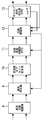
- FIG. 1 is a diagram illustrating a receiving device of a coherent optical communication device according to Embodiment 1 of the present invention.
- the receiving apparatus 1 converts an optical signal received from the optical fiber 2 into an electric signal and performs digital processing.
- the polarization separator 3 separates the optical signal into two orthogonal polarization components. These optical signals and the local light of the local light source 4 are input to the 90 ° hybrid circuits 5 and 6, and a set of output light in which both lights interfere with each other in the same phase and opposite phase, orthogonal (90 °) and inverse orthogonal A total of four output lights of a set of output lights interfered at ( ⁇ 90 °) are obtained. These output lights are converted into analog signals by photodiodes (not shown). These analog signals are converted into digital signals by the AD converter 7.
- the configuration after the chromatic dispersion compensator 8 is an optical transmission distortion compensator that digitally processes the orthogonal modulation signal output as a digital signal from the AD converter 7 to compensate for distortion.
- the chromatic dispersion compensator 8 estimates and compensates for the magnitude of the distortion from the received signal.
- the adaptive equalization unit 9 performs equalization processing to compensate for the distortion.
- the polarization separation is first performed by the optical demodulator, but the polarization separation is more completely processed in the adaptive equalization unit 9.
- a method has been proposed in which a long period / known pattern signal or a short period / known pattern signal is inserted on the transmission side to minimize an error from the received signal.
- the frequency offset compensation unit 10 corrects the frequency error of the local signal (carrier signal) to be transmitted / received.
- the phase fluctuation compensator 11 compensates using a short period / known pattern signal in which residual offset in the frequency offset compensator 10 or residual phase fluctuation or phase slip that cannot be completely removed by the adaptive equalizer 9 is inserted on the transmission side. Process.
- the IQ distortion compensation unit 12 compensates for distortion on the IQ plane (IQ distortion) such as distortion due to DC offset and extinction ratio.
- the IQ distortion compensation is preferably performed in a state where the phase fluctuation and the phase slip are reduced by the frequency offset compensator 10 and the phase fluctuation compensator 11.
- the carrier phase recovery (Carrier Phase Recovery: CPR) unit 13 compensates for phase fluctuations that could not be completely removed by the frequency offset compensation unit 10 and the phase fluctuation compensation unit 11.
- a deviation ⁇ between the temporarily determined constellation (signal point) and the received constellation (signal point) is detected, and the phase is rotated by ⁇ and corrected. Correction by this phase rotation can be performed by multiplying by exp (j ⁇ ).
- the error correction unit 14 performs processing.
- distortion that does not fluctuate statically such as distortion of the optical modulator
- distortion of the optical modulator can be compensated to some extent on the transmission side.
- Compensation on the receiving side has a feature that it is easy to cope with distortion that fluctuates dynamically.
- FIG. 2 is a diagram showing a constellation of 16QAM modulation when there is no distortion.
- FIG. 3 is a diagram showing a 16QAM constellation when distortions of the I component and the Q component occur.
- the distortion of the constellation on the receiving side in optical communication is not a mere offset of DC components, but a bow-like distortion. This is considered due to the nonlinearity of the quadrature modulator and the quadrature demodulator.
- a distortion component that changes in a bow shape on the IQ plane is referred to as a bow-like strain. This bow distortion cannot be compensated by simply offsetting the DC component as in the prior art.
- FIG. 4 is a diagram showing an optical transmission distortion compensation apparatus according to Embodiment 1 of the present invention.
- the IQ distortion compensation unit 12 is installed between the phase fluctuation compensation unit 11 and the carrier phase reproduction unit 13, and includes an I component compensation unit 15, a Q component compensation unit 16, and a coefficient calculation unit 17.
- the I component compensation unit 15 configures a first polynomial of N terms representing distortion of the I component based on the I component Xi and the Q component Xq of the quadrature modulation signal output from the phase fluctuation compensation unit 11, and a coefficient calculation unit By multiplying each term of the first polynomial by the first coefficient for the I component compensator output from 17, the I component with distortion compensated is calculated. If the nth term of the first polynomial composed of the I component and the Q component is INi (n) and the coefficient of the nth term of the first polynomial is hi (n), the output of the I component compensation unit 15 is as follows. It is expressed by the following formula.
- the Q component compensation unit 16 configures a second polynomial of N terms representing the distortion of the Q component based on the I component Xi and the Q component Xq of the quadrature modulation signal output from the phase fluctuation compensation unit 11, and a coefficient calculation unit
- the Q component compensated for distortion is calculated by multiplying each term of the second polynomial by the second coefficient for Q component compensation output from 17. If the nth term of the second polynomial composed of the I component and the Q component is INq (n), and the coefficient of the nth term of the second polynomial is hq (n), the output of the Q component compensation unit 16 is as follows. It is expressed by the following formula.
- the above processing is performed for each symbol, and the coefficient calculation unit 17 optimizes the coefficient of each term independently. Since the coefficient of each term is linear, instantaneous values can be used and no memory is required.
- the carrier phase reproducing unit 13 rotates the phase of the signal vector composed of the I component and the Q component by ⁇ in order to compensate for the phase fluctuation of the outputs of the I component compensation unit 15 and the Q component compensation unit 16. Therefore, the output of the carrier phase reproducing unit 13 is expressed by the following equation.
- the coefficient calculation unit 17 outputs the output of the I component compensation unit 15 and the Q component compensation unit 16 and the reference signal (known signal) for each term of the first and second polynomials before being multiplied by the first and second coefficients. ) To calculate the first and second coefficients. Specifically, the first and second coefficients are calculated so that the error between the output of the carrier phase reproducing unit 13 and the reference signal is minimized. Since the error includes phase rotation compensation in the carrier phase reproducing unit 13, a reverse rotation phase is given to the error and the coefficient calculation unit 17 is supplied to cancel the phase rotation compensation.
- the reference signal for example, a long period / known pattern signal (for example, 256 bits per 10,000 bits) inserted in the transmission signal for synchronization detection can be used. By setting a pseudo random signal as the long period / known pattern signal, the bow distortion of the IQ axis shown in FIG. 3 is easily detected. If only 1 and 0 are repeated, the distortion becomes linear and it is difficult to detect the bow-like distortion.
- FIG. 5 is a diagram showing an I component compensation unit and a Q component compensation unit according to Embodiment 1 of the present invention.
- N 7.
- the distortion is approximated using some terms of Voltera series expansion used as an expression for nonlinearity. This is equivalent to a nonlinear filter.
- the increase / decrease in the number of terms in the first and second polynomials, the use of other axis components, and the increase / decrease in the degree are set based on the technical idea that “bow distortion can be expressed by a polynomial”.
- the output of the I component compensation unit 15 is expressed by the following polynomial based on the I component Xi and the Q component Xq from the phase fluctuation compensation unit 11.
- the output of the Q component compensation unit 16 is represented by the following polynomial based on the I component Xi and the Q component Xq from the phase fluctuation compensation unit 11.
- the bow-shaped distortion changes like a bow along the I axis and changes like a bow along the Q axis. It can be assumed that this can be represented in a pseudo manner by a quadratic curve and a cubic curve for the I component, and a quadratic curve and a cubic curve for the Q component.
- the second term, the third term, and the sixth term in the above formula are intended for this purpose.
- the fifth term is a correction term for preventing the curvature of the bow from changing due to differences in quadrants.
- the first term adjusts the amplitude to account for the difference in amplification ratio during IQ combining on the transmitting side and IQ separation on the receiving side, and further the deviation of the amplitude ratio caused by the load difference in the I component and Q component lines.
- the fourth term is a term for approximating it by a cubic curve and returning it to linear because the control signal of the modulator versus the modulation output has a nonlinearity close to a sine wave.
- the seventh term corresponds to conventional DC offset compensation.
- coefficients hi (1) to hi (7) and the coefficients hq (1) to hq (7) of each term of the polynomial are calculated independently by the coefficient calculation unit 17.
- the outputs of the I component compensation unit 15 and the Q component compensation unit 16 are represented by the following signal vectors.
- the phase of this signal vector is rotated by ⁇ by the phase rotation compensation of the carrier phase reproducing unit 13.
- the output CPR_OUT of the carrier phase reproducing unit 13 is expressed by the following equation.
- the true value of the long period / known pattern signal (reference signal: TSi + jTSq) is subtracted from CPR_OUT to calculate the error err.
- the I component compensation unit 15 and the Q component compensation unit 16 have not yet performed phase rotation compensation by the carrier phase reproduction unit 13. Therefore, if the coefficient calculation is performed using the error err between the result of the phase rotation compensation and the reference signal, the influence of the phase rotation compensation is included, and the coefficient for compensating the IQ distortion cannot be calculated correctly. Therefore, the data input to the coefficient calculation unit 17 is set to err ⁇ e ⁇ j ⁇ by performing an operation for returning the phase rotation compensation to the error err. This is equivalent to performing phase rotation compensation on the reference signal.
- FIG. 6 is a diagram showing a coefficient calculation unit according to Embodiment 1 of the present invention.
- the coefficient calculation unit 17 obtains coefficients of all the polynomial terms of the I component compensation unit 15 and the Q component compensation unit 16 using a least square method (Least Mean Square, LMS) algorithm.
- LMS least Square Mean Square
- the LSM algorithm at this time is represented by the following equation.
- k indicates the number of calculation updates, and is updated for each symbol in the long period / known pattern signal.
- E k is a general error expression input at the k-th time.
- the values of the input signals INi (n), INq (n), error err, and phase rotation amount ⁇ are also different for each k, but k is not shown in the lower expression.
- ⁇ is a coefficient of 1 or less.
- the LSM algorithm uses the following coefficients hi (n) k , hq (n) k , error err ⁇ e ⁇ j ⁇ and input signals Xi, Xq so that the error is minimized.
- the coefficients hi (n) k + 1 and hq (n) k + 1 are obtained.
- the convergence value changes depending on the input status.
- the initial value is not limited to the above example.
- the IQ distortion is expressed by a polynomial, so that constellation distortion that occurs nonlinearly such as bow distortion can be compensated with high accuracy.
- the coefficient calculation unit 17 calculates the first and second coefficients using a least square method algorithm. As a result, the coefficient can be calculated faster and more easily than in the case of using a general minimum mean square error method (Minimum Mean Square Error: MMSE) algorithm.
- MMSE Minimum Mean Square Error
- the coefficient calculation unit 17 calculates the first and second coefficients by using an error between the output of the carrier phase recovery unit 13 and the known signal that has been subjected to compensation processing opposite to the compensation in the carrier phase recovery unit 13. To do. Thereby, the influence of the phase rotation compensation is removed, and the coefficient for compensating the IQ distortion can be calculated with high accuracy, so that the performance of the IQ distortion compensation can be improved.
- the IQ distortion compensation unit 12 by installing the IQ distortion compensation unit 12 at the subsequent stage of the phase fluctuation compensation unit 11, the IQ distortion compensation processing can be performed after the influence of the phase fluctuation is reduced. Therefore, the coefficient for compensating for IQ distortion can be accurately calculated, and the precision of IQ distortion compensation can be improved.
- FIG. FIG. 7 is a diagram showing an optical transmission distortion compensating apparatus according to Embodiment 2 of the present invention.
- a skew compensator 18 is provided between the IQ distortion compensator 12 and the carrier phase regenerator 13. With the addition of the skew compensation unit 18, the coefficient derivation formula in the coefficient calculation unit 17 changes. Other configurations are the same as those of the first embodiment.
- FIG. 8 is a diagram illustrating a skew compensator according to the second embodiment of the present invention.
- the skew compensation unit 18 mainly performs skew compensation that compensates for a delay difference between an I component signal and a Q component signal during transmission.
- the skew compensator 18 uses a filter 19 that performs skew compensation of outputs from the I component compensator 15 and the Q component compensator 16, and an error err subjected to compensation processing opposite to the compensation in the carrier phase regenerator 13.
- a filter coefficient calculation unit 20 that calculates a filter coefficient of the filter 19.
- the filter 19 is a butterfly type FIR filter in consideration of crosstalk between the I component and the Q component.
- the tap coefficients of the respective FIR filters are indicated by t 11 , t 12 , t 21 , and t 22 .
- each has 5 tap coefficients.
- the filter coefficient calculation unit 20 has an LMS algorithm corresponding to each FIR filter.
- the output of the carrier phase reproducing unit 13 is obtained by convolving (t 11 + j ⁇ t 21 ) with INsi which is the Real component of the input of the skew compensator 18 and (t 12 + j ⁇
- the sum of values obtained by convolving t 22 ) is a value obtained by rotating the sum by a phase amount ⁇ .
- the true value of the long period / known pattern signal is subtracted from the output of the carrier phase reproducing unit 13 expressed by the above equation, and the error err is calculated.
- the error err subjected to compensation processing opposite to the compensation in the carrier phase recovery unit 13 (err ⁇ e ⁇ j ⁇ ) is supplied to the LMS algorithm for calculating the coefficient of the FIR filter in the skew compensation unit 18.
- the LMS algorithm for calculating the filter coefficients t 11 and t 12 is supplied with Real [err ⁇ e ⁇ j ⁇ ] that is a real part.
- E k indicates the number of calculation updates.
- the update can be performed for each symbol of the long period / known pattern signal.
- E k is a general error expression input to the LMS at the k-th time. Note that the values of the input signals INsi, INsq, error err, and phase rotation amount ⁇ are different for each k, but the display of k is omitted in the above equation.
- the initial value is not limited to the above example.
- the coefficient calculation unit 17 uses an LMS algorithm to obtain polynomial coefficients hi (n) and hq (n) of the I component compensation unit 15 and the Q component compensation unit 16.
- the formula of the LSM algorithm at that time is shown below.
- E k indicates the number of calculation updates.
- the update can be performed for each symbol of the long period / known pattern signal.
- E k is a general error expression input to the LMS at the k-th time. Note that the values of the input signals INsi, INsq, error err, and phase rotation amount ⁇ are different for each k, but the display of k is omitted in the above equation.
- the initial value is not limited to the above example.
- the error E k input to the LMS algorithm is equal to the error of the skew compensation with respect to the error err calculated at the output of the carrier phase regenerator 13.
- the carrier phase reproduction is restored. In practice, they are given to the reference signal.
- the term added to the right side of the above err is for the purpose of processing.
- the coefficient calculation unit 17 calculates the first and second coefficients by using the error err subjected to the compensation process opposite to the compensation in the skew compensation unit 18 and the carrier phase reproduction unit 13. As a result, the influence of skew and phase rotation compensation can be removed and the coefficient for compensating for IQ distortion can be calculated with high accuracy, so that the performance of IQ distortion compensation can be improved.
- the IQ distortion compensation section 12 is installed at the subsequent stage of the phase fluctuation compensation section 11.
- the IQ distortion compensation unit 12 may be installed in the subsequent stage.
- FIG. 9 is a diagram showing an optical transmission distortion compensating apparatus according to Embodiment 3 of the present invention.
- the adaptive equalization unit 9 and the phase fluctuation compensation unit 11 calculate filter coefficients and compensation amounts for equalization processing and compensation processing based on errors between the known signal and the received signal, respectively.
- a known signal of the adaptive equalization unit 9 a long period for synchronization arranged at the head position of packet data at a level of several hundred symbols, a short period arranged for every several tens of symbols in a known pattern signal or data, A known pattern signal can be used.
- the known signal of the phase fluctuation compensator 11 the short cycle / known pattern signal can be used.
- the adaptive equalization unit 9 and the phase variation compensation unit 11 use the known signal to which the IQ distortion obtained from the calculation result of the coefficient calculation unit 17 is added to filter coefficients for equalization processing and compensation processing. And a compensation amount is calculated. Specifically, IQ distortion is added to a known signal by multiplying or adding a coefficient or compensation amount of an opposite sign. As a result, the coefficient calculation in the adaptive equalization unit 9 and the compensation amount calculation in the phase fluctuation compensation unit 11 can be accurately performed in the equalization process and the compensation process without being affected by the IQ distortion or greatly reduced. Furthermore, the IQ distortion compensation effect can be improved.
- FIG. FIG. 10 is a diagram showing a transmission device of the coherent optical communication device according to Embodiment 4 of the present invention.
- the digital signal processing apparatus of the transmitting apparatus 21 that transmits an optical signal is described.
- DSP Digital Signal Processor
- the modulators 24 and 25 modulate the output light of the signal light source 23 based on the output signal of the DSP 22. These output lights are multiplexed into orthogonal polarization states by the polarization beam combiner 26 and output to the optical fiber 2.
- FIG. 11 is a diagram showing an optical transmission distortion compensating apparatus according to Embodiment 4 of the present invention.
- the IQ distortion compensator 12 on the transmission side predicts the distortion shape by the modulators 24, 25, etc. in the subsequent stage and approximates the distortion with a polynomial.
- the coefficient calculation unit 17 calculates the first and second coefficients so that the error between the output of the I component compensation unit 15 and the Q component compensation unit 16 and the distortion prediction shape is minimized.
- an MMSE algorithm Minimum Mean Square Error, minimum mean square error
- a program for realizing the optical transmission distortion compensation method of Embodiments 1 to 4 is recorded on a computer-readable recording medium, and the program recorded on the recording medium is read into a computer system or a programmable logic device.
- the optical transmission distortion compensation may be performed by executing.
- the “computer system” includes an OS and hardware such as peripheral devices.
- the “computer system” includes a WWW system having a homepage providing environment (or display environment).
- the “computer-readable recording medium” refers to a storage device such as a flexible medium, a magneto-optical disk, a portable medium such as a ROM or a CD-ROM, and a hard disk incorporated in a computer system. Further, the “computer-readable recording medium” refers to a volatile memory (RAM) in a computer system that becomes a server or a client when a program is transmitted via a network such as the Internet or a communication line such as a telephone line. In addition, those holding programs for a certain period of time are also included. The program may be transmitted from a computer system storing the program in a storage device or the like to another computer system via a transmission medium or by a transmission wave in the transmission medium.
- RAM volatile memory
- the “transmission medium” for transmitting the program refers to a medium having a function of transmitting information, such as a network (communication network) such as the Internet or a communication line (communication line) such as a telephone line.
- the program may be for realizing a part of the functions described above. Furthermore, what can implement
Abstract
Description
図1は、本発明の実施の形態1に係るコヒーレント光通信装置の受信装置を示す図である。受信装置1は、光ファイバ2から受信した光信号を電気信号に変換してデジタル処理する。
FIG. 1 is a diagram illustrating a receiving device of a coherent optical communication device according to


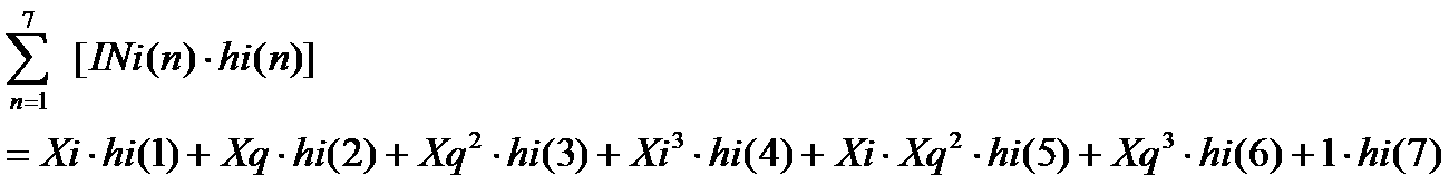


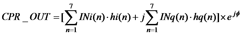


図7は、本発明の実施の形態2に係る光伝送歪補償装置を示す図である。IQ歪補償部12とキャリア位相再生部13との間にSkew補償部18が設けられている。Skew補償部18が加わることに伴い係数算出部17における係数の導出式が変わる。その他の構成は実施の形態1と同様である。
FIG. 7 is a diagram showing an optical transmission distortion compensating apparatus according to


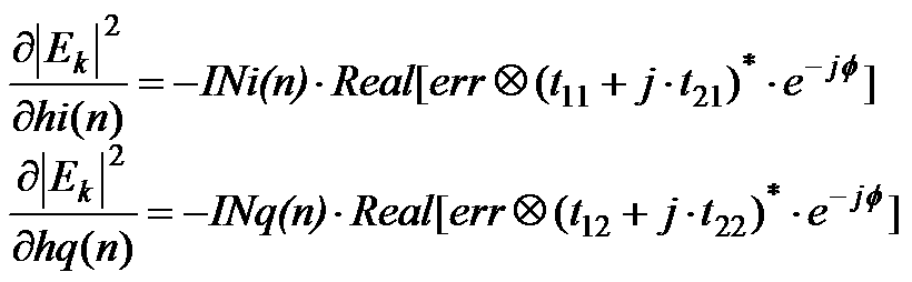
図9は、本発明の実施の形態3に係る光伝送歪補償装置を示す図である。適応等化部9及び位相変動補償部11は、それぞれ既知信号と受信信号との誤差に基づいて等化処理及び補償処理のフィルタ係数及び補償量を算出する。例えば、適応等化部9の既知信号として、パケットデータの先頭位置に数百シンボルレベルで配置される同期用の長周期・既知パターン信号やデータ全体に数十シンボル毎に配置される短周期・既知パターン信号が利用できる。位相変動補償部11の既知信号として、上記短周期・既知パターン信号が利用できる。
FIG. 9 is a diagram showing an optical transmission distortion compensating apparatus according to
図10は、本発明の実施の形態4に係るコヒーレント光通信装置の送信装置を示す図である。実施の形態1~3ではIQ歪補償部12を含む光伝送歪補償装置を受信装置1に適用した場合について説明したが、本実施の形態では光信号を送信する送信装置21のデジタル信号処理装置(Digital Signal Processor: DSP)22に適用している。DSP22の出力信号に基づいて信号光源23の出力光を変調器24,25が変調する。それらの出力光が偏波合成器26によって直交する偏波状態に多重されて光ファイバ2に出力される。
FIG. 10 is a diagram showing a transmission device of the coherent optical communication device according to
Claims (11)
- 直交変調信号のI成分及びQ成分を基にI成分の歪を表す第1の多項式を構成し、第1の係数を前記第1の多項式の各項に乗じることで、歪が補償されたI成分を算出するI成分補償部と、
前記直交変調信号のI成分及びQ成分を基にQ成分の歪を表す第2の多項式を構成し、第2の係数を前記第2の多項式の各項に乗じることで、歪が補償されたQ成分を算出するQ成分補償部と、
前記I成分補償部及び前記Q成分補償部の出力と既知信号とを比較して前記第1及び第2の係数を算出する係数算出部とを備えることを特徴とする光伝送歪補償装置。 A first polynomial representing the distortion of the I component is formed based on the I component and the Q component of the quadrature modulation signal, and the distortion is compensated by multiplying each term of the first polynomial by the first coefficient. An I component compensator for calculating a component;
A second polynomial representing the distortion of the Q component is constructed based on the I component and the Q component of the quadrature modulation signal, and the distortion is compensated by multiplying each term of the second polynomial by the second coefficient. A Q component compensator for calculating the Q component;
An optical transmission distortion compensation apparatus comprising: a coefficient calculation unit that calculates the first and second coefficients by comparing outputs of the I component compensation unit and the Q component compensation unit with known signals. - 前記第1及び第2の多項式の少なくとも一方は、IQ平面上で弓なり状に変化する歪成分を補償する項を含むことを特徴とする請求項1に記載の光伝送歪補償装置。 2. The optical transmission distortion compensation apparatus according to claim 1, wherein at least one of the first and second polynomials includes a term that compensates for a distortion component that changes in a bow shape on the IQ plane.
- 前記弓なり状に変化する歪成分を補償する項として、前記第1の多項式は、Q成分の1次の項、Q成分の2次の項、及びQ成分の3次の項の少なくとも一つを含み、前記第2の多項式は、I成分の1次の項、I成分の2次の項、及びI成分の3次の項の少なくとも一つを含むことを特徴とする請求項2に記載の光伝送歪補償装置。 As a term that compensates for the distortion component that changes in the bow shape, the first polynomial includes at least one of a first-order term of a Q component, a second-order term of a Q component, and a third-order term of a Q component. The second polynomial includes at least one of a first-order term of the I component, a second-order term of the I-component, and a third-order term of the I-component. Optical transmission distortion compensation device.
- 前記第1の多項式はI成分の3次の項を含み、
前記第2の多項式はQ成分の3次の項を含み、
送信変調器の非線形性を補償することを特徴とする請求項1~3の何れか1項に記載の光伝送歪補償装置。 The first polynomial includes a third-order term of I component;
The second polynomial includes a third-order term of a Q component,
4. The optical transmission distortion compensation apparatus according to claim 1, wherein the nonlinearity of the transmission modulator is compensated. - 前記係数算出部は、最小二乗法アルゴリズムを用いて前記第1及び第2の係数を算出することを特徴とする請求項1~4の何れか1項に記載の光伝送歪補償装置。 5. The optical transmission distortion compensation apparatus according to claim 1, wherein the coefficient calculation unit calculates the first and second coefficients using a least square method algorithm.
- 前記I成分補償部及び前記Q成分補償部の出力の位相変動を補償するキャリア位相再生部を更に備え、
前記係数算出部は、前記キャリア位相再生部の出力と前記既知信号との誤差に前記キャリア位相再生部における補償と逆の補償処理を行ったものを用いて前記第1及び第2の係数を算出することを特徴とする請求項1~5の何れか1項に記載の光伝送歪補償装置。 A carrier phase regenerator that compensates for phase fluctuations in the outputs of the I component compensator and the Q component compensator;
The coefficient calculation unit calculates the first and second coefficients by using an error between the output of the carrier phase recovery unit and the known signal that has been subjected to compensation processing opposite to the compensation in the carrier phase recovery unit. 6. The optical transmission distortion compensating apparatus according to claim 1, wherein: - 前記I成分補償部及び前記Q成分補償部と前記キャリア位相再生部との間に設けられたSkew補償部を更に備え、
前記Skew補償部は、前記I成分補償部及び前記Q成分補償部の出力のSkew補償を行うバタフライ型のフィルタと、前記誤差に前記キャリア位相再生部における補償と逆の補償処理を行ったものを用いて前記フィルタのフィルタ係数を算出するフィルタ係数算出部とを有し、
前記係数算出部は、前記誤差に前記Skew補償部及び前記キャリア位相再生部における補償と逆の補償処理を行ったものを用いて前記第1及び第2の係数を算出することを特徴とする請求項6に記載の光伝送歪補償装置。 A skew compensator provided between the I component compensator and the Q component compensator and the carrier phase regenerator;
The skew compensator includes a butterfly filter that performs skew compensation of outputs from the I component compensator and the Q component compensator, and the error subjected to compensation processing opposite to the compensation in the carrier phase reproducing unit. And a filter coefficient calculation unit that calculates a filter coefficient of the filter using,
The coefficient calculation unit calculates the first and second coefficients by using the error obtained by performing a compensation process opposite to the compensation in the skew compensation unit and the carrier phase reproduction unit. Item 7. The optical transmission distortion compensation device according to Item 6. - 前記直交変調信号に等化処理を行う適応等化部と、
前記直交変調信号に補償処理を行う位相変動補償部とを更に備え、
前記I成分補償部及び前記Q成分補償部は前記適応等化部及び前記位相変動補償部の後段に設けられ、
前記適応等化部及び前記位相変動補償部は、前記係数算出部の算出結果から求めたIQ歪を付加した既知信号を用いて前記等化処理及び前記補償処理のフィルタ係数及び補償量を算出することを特徴とする請求項1~7の何れか1項に記載の光伝送歪補償装置。 An adaptive equalization unit for performing equalization processing on the orthogonal modulation signal;
A phase fluctuation compensation unit that performs compensation processing on the quadrature modulation signal;
The I component compensation unit and the Q component compensation unit are provided after the adaptive equalization unit and the phase fluctuation compensation unit,
The adaptive equalization unit and the phase fluctuation compensation unit calculate a filter coefficient and a compensation amount of the equalization process and the compensation process using a known signal to which IQ distortion obtained from the calculation result of the coefficient calculation unit is added. The optical transmission distortion compensating apparatus according to any one of claims 1 to 7, wherein - 光信号を受信する受信装置を備え、
前記受信装置は、請求項1~8の何れか1項に記載の光伝送歪補償装置を有することを特徴とする通信装置。 A receiving device for receiving an optical signal;
9. A communication apparatus comprising the optical transmission distortion compensation apparatus according to claim 1, wherein the reception apparatus includes the optical transmission distortion compensation apparatus according to claim 1. - 光信号を送信する送信装置を備え、
前記送信装置は、請求項1~5の何れか1項に記載の光伝送歪補償装置を有することを特徴とする通信装置。 A transmission device for transmitting an optical signal;
6. A communication apparatus comprising the optical transmission distortion compensation apparatus according to claim 1, wherein the transmission apparatus includes the optical transmission distortion compensation apparatus according to claim 1. - 光伝送歪補償装置が行う光伝送歪補償方法であって、
直交変調信号のI成分及びQ成分を基にI成分の歪を表す第1の多項式を構成し、第1の係数を前記第1の多項式の各項に乗じることで、歪が補償されたI成分を算出するステップと、
前記直交変調信号のI成分及びQ成分を基にQ成分の歪を表す第2の多項式を構成し、第2の係数を前記第2の多項式の各項に乗じることで、歪が補償されたQ成分を算出するステップと、
前記歪が補償されたI成分及びQ成分と既知信号とを比較して前記第1及び第2の係数を算出するステップとを備えることを特徴とする光伝送歪補償方法。 An optical transmission distortion compensation method performed by an optical transmission distortion compensation apparatus,
A first polynomial representing the distortion of the I component is formed based on the I component and the Q component of the quadrature modulation signal, and the distortion is compensated by multiplying each term of the first polynomial by the first coefficient. Calculating a component;
A second polynomial representing the distortion of the Q component is constructed based on the I component and the Q component of the quadrature modulation signal, and the distortion is compensated by multiplying each term of the second polynomial by the second coefficient. Calculating a Q component;
Comparing the distortion-compensated I component and Q component with a known signal to calculate the first and second coefficients, an optical transmission distortion compensation method comprising:
Priority Applications (4)
| Application Number | Priority Date | Filing Date | Title |
|---|---|---|---|
| CN201780036510.6A CN109314683B (en) | 2016-08-29 | 2017-06-21 | Optical transmission distortion compensation device, optical transmission distortion compensation method, and communication device |
| US16/094,857 US10374718B2 (en) | 2016-08-29 | 2017-06-21 | Optical transmission distortion compensation device, optical transmission distortion compensation method, and communication device |
| EP17845848.5A EP3435608B1 (en) | 2016-08-29 | 2017-06-21 | Optical transmission distortion compensation device, optical transmission distortion compensation method, and communication device |
| CA3022078A CA3022078C (en) | 2016-08-29 | 2017-06-21 | Optical transmission distortion compensation device, optical transmission distortion compensation method, and communication device |
Applications Claiming Priority (2)
| Application Number | Priority Date | Filing Date | Title |
|---|---|---|---|
| JP2016167086A JP6315040B2 (en) | 2016-08-29 | 2016-08-29 | Optical transmission distortion compensation apparatus, optical transmission distortion compensation method, and communication apparatus |
| JP2016-167086 | 2016-08-29 |
Publications (1)
| Publication Number | Publication Date |
|---|---|
| WO2018042838A1 true WO2018042838A1 (en) | 2018-03-08 |
Family
ID=61300596
Family Applications (1)
| Application Number | Title | Priority Date | Filing Date |
|---|---|---|---|
| PCT/JP2017/022871 WO2018042838A1 (en) | 2016-08-29 | 2017-06-21 | Optical transmission distortion compensation device, optical transmission distortion compensation method, and communication device |
Country Status (6)
| Country | Link |
|---|---|
| US (1) | US10374718B2 (en) |
| EP (1) | EP3435608B1 (en) |
| JP (1) | JP6315040B2 (en) |
| CN (1) | CN109314683B (en) |
| CA (1) | CA3022078C (en) |
| WO (1) | WO2018042838A1 (en) |
Cited By (4)
| Publication number | Priority date | Publication date | Assignee | Title |
|---|---|---|---|---|
| JP6479278B1 (en) * | 2018-03-09 | 2019-03-06 | 三菱電機株式会社 | Optical receiver and optical transmission / reception system |
| WO2021124415A1 (en) * | 2019-12-16 | 2021-06-24 | 日本電信電話株式会社 | Optical reception device and transmission characteristic estimation method |
| WO2022259367A1 (en) * | 2021-06-08 | 2022-12-15 | 日本電信電話株式会社 | Signal processing method, signal processing device, and communication system |
| JP7415165B2 (en) | 2020-03-19 | 2024-01-17 | 富士通株式会社 | Transmission equipment and distortion compensation method |
Families Citing this family (10)
| Publication number | Priority date | Publication date | Assignee | Title |
|---|---|---|---|---|
| JP6206545B1 (en) * | 2016-06-17 | 2017-10-04 | Nttエレクトロニクス株式会社 | Transmission characteristic compensation apparatus, transmission characteristic compensation method, and communication apparatus |
| JP7059637B2 (en) * | 2018-01-11 | 2022-04-26 | 富士通株式会社 | Signal processing device and signal processing method |
| US11270200B2 (en) * | 2018-02-26 | 2022-03-08 | Nec Corporation | Single-step nonlinearity compensation using artificial intelligence for digital coherent transmission systems |
| CN110365428B (en) * | 2018-04-09 | 2021-09-07 | 富士通株式会社 | Damage monitoring device, damage monitoring and compensating system and method |
| JP7057506B2 (en) * | 2018-09-11 | 2022-04-20 | 日本電信電話株式会社 | Digital coherent receiver and digital coherent receiving method |
| JP6984784B2 (en) * | 2019-02-28 | 2021-12-22 | Nttエレクトロニクス株式会社 | Optical transmission characteristic estimation method, optical transmission characteristic estimation system and optical transmission characteristic compensation system |
| WO2021070280A1 (en) * | 2019-10-09 | 2021-04-15 | 日本電信電話株式会社 | Sn ratio estimating circuit and adaptive filter circuit |
| CN113298246B (en) * | 2021-05-27 | 2023-02-28 | 山东云海国创云计算装备产业创新中心有限公司 | Data processing method, device and computer readable storage medium |
| WO2023067641A1 (en) * | 2021-10-18 | 2023-04-27 | 日本電気株式会社 | Digital signal processing circuit, method, receiver, and communication system |
| CN115941056B (en) * | 2023-03-15 | 2023-05-05 | 北京航空航天大学 | Orthogonal modulation method and device based on microwave photons |
Citations (5)
| Publication number | Priority date | Publication date | Assignee | Title |
|---|---|---|---|---|
| JP2001060883A (en) * | 1999-08-24 | 2001-03-06 | Hitachi Denshi Ltd | Transmitter and data transmission device |
| JP4268760B2 (en) * | 1998-07-16 | 2009-05-27 | エアロフレックス・インターナショナル・リミテッド | Distortion compensation apparatus and method for IQ modulator |
| JP2012182793A (en) | 2006-06-06 | 2012-09-20 | Qualcomm Inc | Fast in-phase and quadrature imbalance calibration |
| JP2016034121A (en) * | 2014-07-31 | 2016-03-10 | 日本電信電話株式会社 | Transmitter |
| JP2016072942A (en) * | 2014-10-02 | 2016-05-09 | 富士通株式会社 | Optical transmitter and waveform distortion correction method |
Family Cites Families (11)
| Publication number | Priority date | Publication date | Assignee | Title |
|---|---|---|---|---|
| GB2348755B (en) * | 1999-04-01 | 2001-03-07 | Wireless Systems Int Ltd | Signal processing |
| JP5287516B2 (en) * | 2009-05-29 | 2013-09-11 | 富士通株式会社 | Digital coherent optical receiver |
| JP2013514027A (en) * | 2009-12-15 | 2013-04-22 | マルチフィ リミテッド | Method and system for coherent equalization of chromatic dispersion of optical signal in fiber |
| EP2381595B1 (en) * | 2010-04-21 | 2012-06-20 | Alcatel Lucent | Phase skew compensation at a coherent optical receiver |
| JP5637065B2 (en) * | 2011-05-13 | 2014-12-10 | 住友電気工業株式会社 | Amplifier circuit and wireless communication device |
| US8811538B1 (en) * | 2013-03-15 | 2014-08-19 | Blackberry Limited | IQ error correction |
| JP6176012B2 (en) * | 2013-09-11 | 2017-08-09 | 富士通株式会社 | Nonlinear distortion compensation apparatus and method, and communication apparatus |
| EP2930865B1 (en) * | 2014-04-07 | 2018-06-06 | Alcatel Lucent | Transmitter quadrature imbalance compensation at a coherent optical receiver |
| CN105264780B (en) * | 2014-05-12 | 2018-06-19 | 华为技术有限公司 | The bearing calibration of receiver mirror image, device and base station |
| JP2016015612A (en) * | 2014-07-02 | 2016-01-28 | 日本電気株式会社 | Receiver and distortion compensation method |
| CN105680946B (en) * | 2016-01-22 | 2018-02-16 | 武汉邮电科学研究院 | A kind of self-adaptive digital signal Processing Algorithm of compensated optical fiber transmission nonlinear impairments |
-
2016
- 2016-08-29 JP JP2016167086A patent/JP6315040B2/en active Active
-
2017
- 2017-06-21 CA CA3022078A patent/CA3022078C/en active Active
- 2017-06-21 US US16/094,857 patent/US10374718B2/en active Active
- 2017-06-21 CN CN201780036510.6A patent/CN109314683B/en active Active
- 2017-06-21 EP EP17845848.5A patent/EP3435608B1/en active Active
- 2017-06-21 WO PCT/JP2017/022871 patent/WO2018042838A1/en active Application Filing
Patent Citations (5)
| Publication number | Priority date | Publication date | Assignee | Title |
|---|---|---|---|---|
| JP4268760B2 (en) * | 1998-07-16 | 2009-05-27 | エアロフレックス・インターナショナル・リミテッド | Distortion compensation apparatus and method for IQ modulator |
| JP2001060883A (en) * | 1999-08-24 | 2001-03-06 | Hitachi Denshi Ltd | Transmitter and data transmission device |
| JP2012182793A (en) | 2006-06-06 | 2012-09-20 | Qualcomm Inc | Fast in-phase and quadrature imbalance calibration |
| JP2016034121A (en) * | 2014-07-31 | 2016-03-10 | 日本電信電話株式会社 | Transmitter |
| JP2016072942A (en) * | 2014-10-02 | 2016-05-09 | 富士通株式会社 | Optical transmitter and waveform distortion correction method |
Non-Patent Citations (2)
| Title |
|---|
| See also references of EP3435608A4 |
| SUGIHARA TAKASHI: "Recent Progress of Pre-equalization Technology for High-speed Optical Communication", THE INSTITUTE OF ELECTRONICS, INFORMATION AND COMMUNICATION ENGINEERS, SHINGAKUGIHOU, IEICE TECHNICAL REPORT, OCS2011-41, July 2011 (2011-07-01), pages 83 - 88 |
Cited By (7)
| Publication number | Priority date | Publication date | Assignee | Title |
|---|---|---|---|---|
| JP6479278B1 (en) * | 2018-03-09 | 2019-03-06 | 三菱電機株式会社 | Optical receiver and optical transmission / reception system |
| WO2019171587A1 (en) * | 2018-03-09 | 2019-09-12 | 三菱電機株式会社 | Optical receiver and optical transmission/reception system |
| WO2021124415A1 (en) * | 2019-12-16 | 2021-06-24 | 日本電信電話株式会社 | Optical reception device and transmission characteristic estimation method |
| JPWO2021124415A1 (en) * | 2019-12-16 | 2021-06-24 | ||
| JP7303459B2 (en) | 2019-12-16 | 2023-07-05 | 日本電信電話株式会社 | Optical receiver and transmission characteristic estimation method |
| JP7415165B2 (en) | 2020-03-19 | 2024-01-17 | 富士通株式会社 | Transmission equipment and distortion compensation method |
| WO2022259367A1 (en) * | 2021-06-08 | 2022-12-15 | 日本電信電話株式会社 | Signal processing method, signal processing device, and communication system |
Also Published As
| Publication number | Publication date |
|---|---|
| CA3022078C (en) | 2020-02-18 |
| JP2018037735A (en) | 2018-03-08 |
| US10374718B2 (en) | 2019-08-06 |
| US20190132051A1 (en) | 2019-05-02 |
| CN109314683A (en) | 2019-02-05 |
| CN109314683B (en) | 2021-06-01 |
| EP3435608A1 (en) | 2019-01-30 |
| EP3435608B1 (en) | 2021-01-13 |
| CA3022078A1 (en) | 2018-03-08 |
| JP6315040B2 (en) | 2018-04-25 |
| EP3435608A4 (en) | 2019-11-06 |
Similar Documents
| Publication | Publication Date | Title |
|---|---|---|
| JP6315040B2 (en) | Optical transmission distortion compensation apparatus, optical transmission distortion compensation method, and communication apparatus | |
| Khanna et al. | A robust adaptive pre-distortion method for optical communication transmitters | |
| JP6206545B1 (en) | Transmission characteristic compensation apparatus, transmission characteristic compensation method, and communication apparatus | |
| JP6156807B2 (en) | Received signal processing apparatus, communication system, and received signal processing method | |
| JP5406989B2 (en) | Optical receiver and optical transmission system | |
| US8131148B2 (en) | Optical transmitter error reduction using receiver feedback | |
| CN107925485B (en) | Coherent light receiving device | |
| US20190149393A1 (en) | Nonlinearity pre-compensation of high order modulation transmissions | |
| US11539447B2 (en) | Subcarrier based adaptive equalization of electrical filtering effects on sub-carrier multiplexed signals | |
| Lagha et al. | Blind Joint Polarization Demultiplexing and IQ Imbalance Compensation for $ M $-QAM Coherent Optical Communications | |
| US10708035B2 (en) | Signal processing device and signal processing method | |
| CN108521385B (en) | Coherent optical communication equalization method using cross hybrid state | |
| Zhang et al. | Training symbol-based equalization for quadrature duobinary PDM-FTN systems | |
| US20220216923A1 (en) | Optical transmission system and compensation method | |
| Shu et al. | Experimental investigation of extended Kalman Filter combined with carrier phase recovery for 16-QAM system | |
| Nguyen-Ti et al. | Blind I/Q imbalance compensation for m-QAM optical coherent systems based on pseudo-rotation | |
| WO2017069086A1 (en) | Coherent light-receiving device | |
| WO2023119627A1 (en) | Gain adjustment method, optical reception device, and computer program | |
| US11736199B1 (en) | Systems and methods for phase compensation | |
| US11546058B1 (en) | Systems and methods for chromatic dispersion pre-compensation | |
| US20230085546A1 (en) | Perturbative-based nonlinear compensation for digital subcarrier systems | |
| WO2023248285A1 (en) | Multicarrier signal waveform equalization circuit and multicarrier signal waveform equalization method | |
| CN117768037A (en) | Cascading MIMO structure for ultra-high order coherent light transmission system | |
| Gong et al. | Coherent optical transmitter IQ imbalance mitigation with embedded carrier phase and frequency offset estimation | |
| WO2017169424A1 (en) | Optical signal reception apparatus, optical communication system, and method for generating compensation signal for optical signal reception apparatus |
Legal Events
| Date | Code | Title | Description |
|---|---|---|---|
| ENP | Entry into the national phase |
Ref document number: 3022078 Country of ref document: CA |
|
| WWE | Wipo information: entry into national phase |
Ref document number: 2017845848 Country of ref document: EP |
|
| ENP | Entry into the national phase |
Ref document number: 2017845848 Country of ref document: EP Effective date: 20181025 |
|
| 121 | Ep: the epo has been informed by wipo that ep was designated in this application |
Ref document number: 17845848 Country of ref document: EP Kind code of ref document: A1 |
|
| NENP | Non-entry into the national phase |
Ref country code: DE |