WO2018037889A1 - 光変調器モジュール - Google Patents
光変調器モジュール Download PDFInfo
- Publication number
- WO2018037889A1 WO2018037889A1 PCT/JP2017/028523 JP2017028523W WO2018037889A1 WO 2018037889 A1 WO2018037889 A1 WO 2018037889A1 JP 2017028523 W JP2017028523 W JP 2017028523W WO 2018037889 A1 WO2018037889 A1 WO 2018037889A1
- Authority
- WO
- WIPO (PCT)
- Prior art keywords
- modulation element
- light modulation
- socket
- circuit board
- light
- Prior art date
- Legal status (The legal status is an assumption and is not a legal conclusion. Google has not performed a legal analysis and makes no representation as to the accuracy of the status listed.)
- Ceased
Links
Images



Classifications
-
- G—PHYSICS
- G02—OPTICS
- G02B—OPTICAL ELEMENTS, SYSTEMS OR APPARATUS
- G02B27/00—Optical systems or apparatus not provided for by any of the groups G02B1/00 - G02B26/00, G02B30/00
- G02B27/01—Head-up displays
-
- G—PHYSICS
- G03—PHOTOGRAPHY; CINEMATOGRAPHY; ANALOGOUS TECHNIQUES USING WAVES OTHER THAN OPTICAL WAVES; ELECTROGRAPHY; HOLOGRAPHY
- G03B—APPARATUS OR ARRANGEMENTS FOR TAKING PHOTOGRAPHS OR FOR PROJECTING OR VIEWING THEM; APPARATUS OR ARRANGEMENTS EMPLOYING ANALOGOUS TECHNIQUES USING WAVES OTHER THAN OPTICAL WAVES; ACCESSORIES THEREFOR
- G03B21/00—Projectors or projection-type viewers; Accessories therefor
- G03B21/14—Details
-
- G—PHYSICS
- G09—EDUCATION; CRYPTOGRAPHY; DISPLAY; ADVERTISING; SEALS
- G09F—DISPLAYING; ADVERTISING; SIGNS; LABELS OR NAME-PLATES; SEALS
- G09F9/00—Indicating arrangements for variable information in which the information is built-up on a support by selection or combination of individual elements
Definitions
- the present invention relates to an optical modulator module using a reflective optical modulation element.
- the projection display device is a device that projects image light (projection light) obtained by optically modulating illumination light emitted from the illumination optical system with a reflective light modulation element onto a screen or the like.
- Examples of the reflective light modulation element include DMD (registered trademark: Digital Micromirror Device).
- the DMD is typically an LGA (Land Grid Array) package, and the terminal of the DMD and the contact of the socket are electrically connected by pressing the terminal side against a dedicated socket.
- An object of the present invention is to provide an optical modulator module that can favorably maintain the electrical connection of the optical modulation elements.
- the light modulator module of the present invention receives illumination light from the front surface side, and a plurality of reflective surfaces that reflect the image light modulated by the illumination light in a predetermined direction on the front surface side and a plurality of arrays on the surface opposite to the reflection surface
- a light modulation element having a pin-shaped terminal, and a first contact disposed on a back side of the light modulation element, into which the terminal of the light modulation element is inserted and electrically connected to the terminal
- a socket having a pin-like second contact electrically connected to the first contact and arranged on a surface opposite to the surface on which the first contact is provided, and on the front side of the light modulation element Arranged and urged the light modulation element to the socket side in contact with the light modulation element, and a mounting plate for holding the light modulation element between the socket and the rear side of the socket, Insert the second contact
- a circuit board having a through hole for mounting the socket; a heat dissipating part disposed on the back side of the circuit board and
- the electrical connection of the light modulation element can be maintained well.
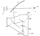
- FIG. 1 It is a figure which shows the structure of the head-up display by which the projection type display apparatus which concerns on this invention is mounted. It is a figure which shows the example of a structure of the projection type display apparatus of FIG. It is a disassembled perspective view of the projection type display apparatus of FIG. It is a perspective view of the projection type display apparatus of FIG. 1 assembled. It is sectional drawing of the light modulation element module of FIG. It is sectional drawing of the modification of the light modulation element module of FIG.
- the projection display apparatus 100 is applied to, for example, a head-up display 1 mounted on a vehicle.
- a head-up display 1 includes a projection display device 100 that generates image light L, a screen 200 that receives the image light L generated by the projection display device 100 and displays an image (real image), and a screen 200.
- a plane mirror 300 that reflects the image light L emitted from the mirror
- a concave mirror 400 that reflects the image light L reflected by the plane mirror 300 toward the front windshield (transmission reflection portion) 2.
- the projection display device 100, the screen 200, the plane mirror 300, and the case body 500 that houses the concave mirror 400 are configured, and the virtual image V is displayed forward through the front windshield 2 when viewed from the user.
- the user can visually recognize the virtual image V by placing the viewpoint 3a in the eye box 3 which is a predetermined area generated by the head-up display 1.
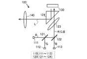
- FIG. 2 is a diagram showing an example of the configuration of the light distribution member of the projection display apparatus 100.
- the projection display apparatus 100 distributes a red light source 111 that emits red light R, a green light source 112 that emits green light G, a blue light source 113 that emits blue light B, and light rays (illumination light) R, G, and B.
- the light distribution member 120, the light modulation element 130 that converts the distributed light into the image light L, and the light projection lens 140 that forms an image of the image light L from the light modulation element 130 on the screen 200 are mainly used. Composed.
- the light distribution member 120 includes, for example, dichroic mirrors 121 and 122, a convex lens 123, a prism 124, and the like.
- the red light R passes through the dichroic mirror 121, is reflected by the dichroic mirror 122, and travels toward the convex lens 123.
- the green light beam G is reflected by the dichroic mirror 121 and further reflected by the dichroic mirror 122 toward the convex lens 123.
- the blue light B passes through the dichroic mirror 122, and the transmitted light goes to the convex lens 123.
- the light rays R, G, and B are distributed by the convex lens 123, pass through the prism 124, and reach the light modulation element 130.
- the light modulation element 130 modulates the light into a predetermined image light L.
- the modulated image light L is reflected by the prism 124, and the reflected image light L passes through the light projection lens 140 and is projected (emitted).
- FIG. 3 is an exploded perspective view of the projection display apparatus 100.
- the projection display device 100 includes a housing 150 that houses the light distribution member 120 described in FIG. 1, and a red light source (FIG. 1, reference numeral attached to the first wall 151 of the housing 150. 111), a second substrate 112a mounted on the second wall 152 of the housing 150 and mounting a green light source (FIG. 1, reference numeral 112), and mounted on the second wall 152 of the housing 150.
- the housing 150 accommodates the light distribution member 120 inside, and is made of a resin containing filler or metal to which a filler having high thermal conductivity is added.
- the housing 150 includes, for example, a rectangular first wall 151, a second wall 152, and a third wall 153 in a part of the outer wall.
- casing 150 is not restricted to what was mentioned above, You may add or abbreviate
- the first wall 151 of the housing 150 includes a rectangular first window 151a
- the second wall 152 includes a rectangular second window 152a and a third window 152b
- the third wall 153 includes: A rectangular fourth window (not shown) is provided.
- a first substrate 111 a is attached to the first wall 151, and a red light source 111 mounted on the first substrate 111 a is disposed on the first window portion 151 a so as to face the inside of the housing 150.
- the second substrate 112a and the third substrate 113a are attached to the second wall 152, and the second window portion 152a and the third window portion 152b are mounted on the second substrate 112a and the third substrate 113a.
- the light source 112 and the blue light source 113 are arranged so as to face the inside of the housing 150. Further, a light modulation element module 160 (to be described later) is attached to the third wall 153, and the light modulation element 130 in the light modulation element module 160 is attached to the casing 150 in the fourth window provided on the third wall 153. It is arranged to face the inside.
- the shape of the housing 150 is arbitrary. Further, the three substrates 111a, 112a, and 113a may all be attached to a common wall, for example, the second wall 152, or the three substrates 111a, 112a, and 113a may be attached to different walls. That is, the layout of the three substrates 111a, 112a, and 113a with respect to the housing 150 is arbitrary.
- the projection display apparatus 100 is fixed to the apparatus base 510 with screws M1.
- the projection display device 100 may be bonded and fixed to the device base 510.
- the device base 510 is a part of the case body 500 that houses the projection display device 100 of the head-up display 1, the screen 200, the relay optical system (planar mirror 300, concave mirror 400), and the like, and is a metal made of aluminum alloy or carbon steel. It is desired to be made.
- the first to third substrates 111a, 112a, 113a are detachably attached to the housing 150 with screws M2.
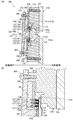
- FIG. 5 is a cross-sectional view of the light modulation element module 160 when attached to the third wall 153 of the housing 150.
- the light modulation element module 160 is a module formed by assembling a light modulation element 130, a socket 133 to which the light modulation element 130 is attached, a mounting plate 170, a circuit board 180, a cushion portion 190, and a heat radiating portion 195.
- the assembled light modulation element module 160 is fixed to the housing 150 with a screw M3.
- the light modulation element 130 is, for example, a reflective display device such as DMD or LCOS (registered trademark: Liquid Crystal On Silicon), and a plurality of pin-shaped terminals 131 are two-dimensionally provided on the opposite side (back side) of the reflective surface.
- the plurality of terminals 131 are housed and fixed in the socket 133 so as to be inserted into first contacts 134 of the socket 133 described later and to be electrically connected.
- the plurality of terminals 131 are disposed in a region excluding the central region of the light modulation element 130, and a rectangular heat radiation terminal 132 is disposed in the central region in order to release the heat of the light modulation element 130.
- the socket 133 is formed of an insulating resin in a concave shape so that the light modulation element 130 can be accommodated in a substantially central portion, and the concave bottom surface 135 is a plane having a rectangular opening 136 in the central region. ing.
- a plurality of first holes are formed in the bottom surface 135 so as to surround the opening 136, and a conductive first contact 134 is accommodated in the plurality of holes.
- a plurality of second holes are formed on the back surface of the socket 133 so as to surround the opening 136.
- the plurality of second holes (not shown) are electrically connected to the plurality of first contacts 134, respectively.
- a plurality of second contacts 137 connected to are housed so as to protrude somewhat.
- the first contact 134 is formed in a U-shape, and is disposed so that the U-shaped opening faces the entrance side of the first hole portion.
- the terminal 131 of the PGA package of the light modulation element 130 is connected to the first hole.
- the U-shaped opening of the first contact 134 is expanded and the pin-shaped terminal 131 of the light modulation element 130 is fitted to the first contact 134 so that the light modulation element 130 is electrically connected.
- Contact The plurality of second contacts 137 that are electrically connected to the first contacts 134 and project from the back side of the socket 133 are inserted into the through holes 181 of the circuit board 180 and are electrically connected by soldering.
- the second contact 137 desirably protrudes about 0.5 mm from the back side of the circuit board 180 when inserted into the through hole 181 of the circuit board 180.
- the second contact 137 may be a press-fit terminal that is press-fitted into the through hole 181 of the circuit board 180 instead of soldering.
- the second contact 137 may be provided with a standoff 139 that forms a gap between the back surface of the socket 133 and the circuit board 180. Since a gap is formed between the back surface of the socket 133 and the circuit board 180, air permeability in the through hole 181 is improved, so that melted solder easily enters the through hole 181 and good solder is obtained. In addition, it is possible to suppress the occurrence of solder bridge between the pin-shaped second contacts 137.
- the socket 133 has a protrusion (positioning portion) 138, and the protrusion 133 is inserted into an attachment hole 172 of the attachment plate 170, which will be described later, so that the socket 133 containing the light modulation element 130 is attached to the attachment plate 170. Is positioned.
- the positioning unevenness relationship between the socket 133 and the mounting plate 170 may be reversed.
- the positioning may be replaced by engaging the members, and the positioning structure itself may be omitted.
- the mounting plate 170 has a display hole 171 through which the light beams R, G, and B incident on the light modulation element 130 and the image light L reflected by the light modulation element 130 pass, and a mounting hole 172 into which the projection 138 of the socket 133 is inserted.
- a through hole 173 into which a screw M3 described later is inserted, and a boss 175 formed with a heat radiating portion 195 and a screw M4, which are described later, and projecting toward the heat radiating portion 195, and a light modulation element module This is a member that comes into contact with the housing 150 when 160 is attached to the housing 150.
- the mounting plate 170 is a member having a lower thermal conductivity than the housing 150, and is formed of, for example, a resin material such as polycarbonate, a low thermal conductivity metal such as stainless steel or titanium, and the like. For this reason, since the amount of heat transfer from the housing 150 to the light modulation element 130 can be suppressed, the light source from the housing 150 housing the light distribution member 120 while suppressing the influence of heat generation of the light source 110 on the light modulation element 130. The heat of 110 can be radiated smoothly.
- the circuit board 180 is formed of a hard base material, and a plurality of through holes 181 into which the plurality of pin-shaped second contacts 137 of the socket 133 are inserted are formed, and a rectangular opening is formed in the central region. 182 is formed, and a positioning hole 183 into which the boss 175 of the mounting plate 170 is inserted is formed.
- the circuit board 180 is connected to the control unit by a wiring (not shown), and supplies an electrical signal and power from the control unit to the light modulation element 130 through the through hole 181.
- the circuit board 180 is pressed against the mounting plate 170 by the heat radiating portion 195 and the cushion portion 190 when the heat radiating portion 195 described later is fastened to the mounting plate 170 using the screws M4. It is held between the cushion part 190.
- the cushion portion 190 is made of, for example, a plate-like member having elasticity and insulating properties such as urethane, and the second contact 137 of the socket 133 and the through hole 181 of the circuit board 180 are connected (soldered). A rectangular opening 191 is formed in the central region. That is, the cushion portion 190 is disposed at a position overlapping the second contact 137 in a plan view in the thickness direction (assembly direction).
- the cushion part 190 is disposed between the circuit board 180 and a heat radiating part 195 described later. When the heat radiating part 195 is fastened to the mounting plate 170 using the screws M4, the cushion part 190 and the heat radiating part 195 described later are radiated.
- the circuit board 180 is pressed against the socket 133 (second contact 137) side by an elastic force that is compressed between the portion 195 and returns to the original shape.
- the thickness of the cushion part 190 is set to be longer than the length of the second contact 137 protruding from the back side of the socket 133 even when the cushion part 190 is compressed between the circuit board 180 and a heat radiating part 195 described later. Is done. Since the circuit board 180 is pressed to the front side (front side) by the elastic force of the cushion portion 190 in this way, the force applied to the circuit board 180 and the light modulation element 130 due to vibration or the like is absorbed, and the load applied to each component is reduced. Can be reduced.
- the socket 133 of the PGA package since it is firmly bonded to the circuit board 180, it is possible to prevent the electrical connection from being disconnected due to vibration or the like, and to protrude from the back surface of the socket 133. It is possible to prevent the second contact 137 from contacting the conductive heat radiation part 195.
- the heat dissipating part 195 is a hard plate-like member disposed on the back side of the cushion part 190, and in the central region, a plurality of projecting parts 196 projecting to the front side and projecting to the side opposite to the mounting plate 170 side. It has the radiation fin 197 (refer FIG. 3) and the through-hole 198 which the screw
- the heat dissipating part 195 inserts the protruding part 196 into the opening 136 of the socket 133, the opening 182 of the circuit board 180, and the opening 191 of the cushion part 190, respectively.
- the heat radiating portion 195 is inserted into the through-hole 198 with a screw M4, which will be described later, and fastened to the mounting plate 170, so that the socket 133 storing the light modulation element 130, the circuit board 180, and the cushion portion 190 are connected.
- the protrusion 196 is in direct contact with the heat radiating terminal 132 of the light modulation element 130.
- a member such as silicon rubber having high elasticity and thermal conductivity may be sandwiched between the protruding portion 196 of the heat radiating portion 195 and the heat radiating terminal 132 of the light modulation element 130.
- the light modulation element 130 is housed and fixed in the socket 133, and the socket 133 is mounted on the circuit board 180.
- the positioning hole 183 of the circuit board 180 on which the socket 133 is mounted is inserted into the boss 175 of the mounting plate 170.
- the cushion part 190 is disposed on the back side of the circuit board 180.
- the light modulation element module 160 is assembled.
- the light modulation element module 160 can be fixed to the casing 150 by inserting a screw M3 through a through hole 173 provided in the mounting plate 170 of the light modulation element module 160 and screwing the screw M3 to the casing 150. it can.
- the first embodiment has been described as an example of the technique disclosed in the present application.
- the technology in the present disclosure is not limited to this, and can be applied to an embodiment in which changes, replacements, loads, omissions, and the like are made without departing from the gist of the present invention.
- the shapes and fixing structures of the light modulation element 130, the socket 133, the mounting plate 170, the circuit board 180, the cushion portion 190, the heat dissipation portion 195, and the like are not limited to the shapes of the above embodiments.
- the cushion portion 190 is disposed at a position overlapping the second contact 137 in the plan view in the thickness direction.
- position in the position which does not overlap with the contact 137.
- a gap can be provided so that the second contact 137 of the socket 133 does not contact the heat radiating part 195.
- the light modulator module of the present invention is suitable for a display device mounted on a vehicle.
- heat exhausting member 200 ... screen, 300 ... plane mirror (relay) Optical system), 400 ... concave mirror (relay optical system), 500 ... case body, L ... image light, M1 to M4 ... screw (screw), ... virtual image
Landscapes
- Physics & Mathematics (AREA)
- General Physics & Mathematics (AREA)
- Optics & Photonics (AREA)
- Engineering & Computer Science (AREA)
- Theoretical Computer Science (AREA)
- Cooling Or The Like Of Electrical Apparatus (AREA)
Abstract
光変調素子の電気的な接続を良好に維持できる。 PGAパッケージの光変調素子130を、ピン状の第2コンタクト137を有するソケット133に装着し、このソケット133を回路基板180のスルーホール実装し、取付板170の背面側に回路基板180を配設し、回路基板180の背面側に光変調素子130の熱を放熱可能な放熱部195を設け、回路基板180と放熱部195との間に弾性および絶縁性を有するクッション部190を配設し、放熱部195と取付板170とを固定することで、内部に光変調素子130、ソケット133、回路基板180およびクッション部190を挟持し、クッション部190は、回路基板180から突出した第2コンタクト137が放熱部195に接触しないように、回路基板180と放熱部195との間に隙間を設ける。
Description
本発明は、反射型の光変調素子を用いた光変調器モジュールに関する。
投写型表示装置は、照明光学系から出射された照明光を反射型の光変調素子で光変調した画像光(投影光)を、スクリーンなどへ投写する装置である。反射型の光変調素子としては、例えば、DMD(登録商標:Digital Micromirror Device)などがある。DMDは、典型的には、LGA(Land Grid Array)パッケージであり、端子側を専用のソケットに押し当てることで、DMDの端子とソケットのコンタクトとが電気的に接続される。
しかしながら、光変調素子をソケットに押し当てることで電気的な接続を図った場合、振動や温度変化による部品の膨張に起因して、光変調素子の端子とソケットに設けられたコンタクトとの接触が離れてしまい、光変調素子が誤動作してしまうおそれがあった。
本発明は、光変調素子の電気的な接続を良好に維持できる光変調器モジュールを提供することを課題とする。
本発明の光変調器モジュールは、照明光を前面側から受光し、この照明光を変調した画像光を前面側の所定の方向に反射する反射面と、前記反射面と反対の面に複数配列されたピン状の端子と、を有する光変調素子と、前記光変調素子の背面側に配置され、前記光変調素子の前記端子が挿入され、前記端子と電気的に接続される第1コンタクトと、前記第1コンタクトと電気的に接続され、前記第1コンタクトが設けられた面の反対の面に配列されたピン状の第2コンタクトと、を有するソケットと、前記光変調素子の前面側に配置されると共に前記光変調素子に接して前記光変調素子を前記ソケット側へ付勢し、前記ソケットとの間で前記光変調素子を保持する取付板と、前記ソケットの背面側に配置され、前記第2コンタクトを挿入して前記ソケットを実装するスルーホールを有する回路基板と、前記回路基板の背面側に配置され、前記光変調素子と間接または直接熱伝導的に接続される放熱部と、前記放熱部と前記回路基板との間に配置されると共に前記放熱部と前記回路基板とにそれぞれ接して、弾性及び絶縁性を有するクッション部と、を備える。
本発明では、光変調素子の電気的な接続を良好に維持できる。
本発明の実施の形態を添付図に基づいて以下に説明する。
図1に示されるように、投写型表示装置100は、例えば、車両に搭載されるヘッドアップディスプレイ1に適用される。このようなヘッドアップディスプレイ1は、画像光Lを生成する投写型表示装置100と、投写型表示装置100が生成した画像光Lを受光して画像(実像)を表示するスクリーン200と、スクリーン200から出射される画像光Lを反射する平面鏡300(リレー光学系)と、平面鏡300が反射した画像光Lをフロントウインドシールド(透過反射部)2に向けて反射する凹面鏡400(リレー光学系)と、これら投写型表示装置100とスクリーン200と平面鏡300と凹面鏡400とを収納するケース体500と、から構成され、ユーザから見てフロントウインドシールド2を介した前方に虚像Vを表示する。ユーザは、ヘッドアップディスプレイ1が生成する所定の領域であるアイボックス3内に視点3aを置くことで虚像Vを視認することが可能となる。
図2は、投写型表示装置100の配光部材の構成の例を示す図である。投写型表示装置100は、赤色光線Rを発する赤色光源111と、緑色光線Gを発する緑色光源112と、青色光線Bを発する青色光源113と、光線(照明光)R、G、Bを配光する配光部材120と、配光された光を画像光Lに変換する光変調素子130と、光変調素子130からの画像光Lをスクリーン200に結像させる投光レンズ140と、から主に構成される。
配光部材120は、例えば、ダイクロイックミラー121,122、凸レンズ123、プリズム124等とからなる。
赤色光線Rはダイクロイックミラー121を透過し、ダイクロイックミラー122で反射して凸レンズ123へ向かう。
緑色光線Gはダイクロイックミラー121で反射し、さらにダイクロイックミラー122で反射して凸レンズ123へ向かう。
青色光線Bはダイクロイックミラー122を透過し、透過光は凸レンズ123へ向かう。
緑色光線Gはダイクロイックミラー121で反射し、さらにダイクロイックミラー122で反射して凸レンズ123へ向かう。
青色光線Bはダイクロイックミラー122を透過し、透過光は凸レンズ123へ向かう。
光線R、G、Bは、凸レンズ123で配光され、プリズム124を透過し、光変調素子130に至る。この光変調素子130で所定の画像光Lに変調される。変調された画像光Lは、プリズム124で反射され、反射された画像光Lは、投光レンズ140を透過して投写(出射)される。
図3は、投写型表示装置100の分解斜視図である。
図3に示すように、投写型表示装置100は、図1で説明した配光部材120を収納する筐体150と、この筐体150の第1壁151に取付けられ赤色光源(図1、符号111)を実装する第1基板111aと、筐体150の第2壁152に取付けられ緑色光源(図1、符号112)を実装する第2基板112aと、筐体150の第2壁152に取付けられ青色光源(図1、符号113)を実装する第3基板113aと、光変調素子130を含み、筐体150の第3壁153に取付けられる光変調素子モジュール160と、を備える。
図3に示すように、投写型表示装置100は、図1で説明した配光部材120を収納する筐体150と、この筐体150の第1壁151に取付けられ赤色光源(図1、符号111)を実装する第1基板111aと、筐体150の第2壁152に取付けられ緑色光源(図1、符号112)を実装する第2基板112aと、筐体150の第2壁152に取付けられ青色光源(図1、符号113)を実装する第3基板113aと、光変調素子130を含み、筐体150の第3壁153に取付けられる光変調素子モジュール160と、を備える。
筐体150は、配光部材120を内部に収納するものであり、熱伝導率の高いフィラーが添加されているフィラー入り樹脂、又は金属で構成される。
筐体150は、外壁の一部に、例えば、矩形の第1壁151、第2壁152、第3壁153を有する。なお、筐体150に収納される配光部材120は、前述したものに限られず、適宜追加、または省略してもよい。
筐体150は、外壁の一部に、例えば、矩形の第1壁151、第2壁152、第3壁153を有する。なお、筐体150に収納される配光部材120は、前述したものに限られず、適宜追加、または省略してもよい。
筐体150の第1壁151は、矩形の第1窓部151aを有し、第2壁152は、矩形の第2窓部152a及び第3窓部152bを有し、第3壁153は、矩形の図示しない第4窓部を有している。第1壁151には、第1基板111aが取付けられ、第1窓部151aには、第1基板111aに実装される赤色光源111が筐体150の内部を臨むように配置される。また、第2壁152には、第2基板112a、第3基板113aが取付けられ、第2窓部152a、第3窓部152bには、第2基板112a、第3基板113aに実装される緑色光源112、青色光源113が筐体150の内部を臨むように配置される。さらに、第3壁153には、後述する光変調素子モジュール160が取付けられ、第3壁153に設けられた前記第4窓部には、光変調素子モジュール160における光変調素子130が筐体150の内部を臨むように配置される。
なお、筐体150の形状は任意である。また、3個の基板111a,112a,113aは、共通の壁、例えば第2壁152に全て取付けることや、3個の基板111a,112a,113aを異なる壁に取付けてもよい。すなわち、筐体150に対する3個の基板111a,112a,113aのレイアウトは任意である。
図4に示すように、投写型表示装置100は、ビスM1により、装置ベース510に固定される。なお、投写型表示装置100は、装置ベース510に接着固定されてもよい。
装置ベース510は、ヘッドアップディスプレイ1の投写型表示装置100、スクリーン200、リレー光学系(平面鏡300、凹面鏡400)などを収納するケース体500の一部であり、アルミニウム合金又は炭素鋼からなる金属製であることが望まれる。また、第1~第3基板111a、112a,113aは、ビスM2で筐体150に取り外し可能に取付けられる。
装置ベース510は、ヘッドアップディスプレイ1の投写型表示装置100、スクリーン200、リレー光学系(平面鏡300、凹面鏡400)などを収納するケース体500の一部であり、アルミニウム合金又は炭素鋼からなる金属製であることが望まれる。また、第1~第3基板111a、112a,113aは、ビスM2で筐体150に取り外し可能に取付けられる。
続いて、図5を用いて光変調素子モジュール160について説明する。図5は、筐体150の第3壁153に取付けられた際の光変調素子モジュール160の断面図である。光変調素子モジュール160は、光変調素子130と、光変調素子130を取り付けるソケット133と、取付板170と、回路基板180と、クッション部190と、放熱部195と、を組み付けてモジュール化したものであり、組み付けられた光変調素子モジュール160は、ねじM3により、筐体150に固定される。
光変調素子130は、例えば、DMDやLCOS(登録商標:Liquid Crystal On Silicon)などの反射型の表示デバイスであり、反射面の反対側(背面側)に複数のピン状の端子131を二次元的に配列したPGAパッケージ構造を有し、この複数の端子131が後述するソケット133の第1コンタクト134に挿入されて電気的に接続されるようにソケット133に収納固定される。また、これら複数の端子131は、光変調素子130の中央領域を除く領域に配置され、中央領域には、光変調素子130の熱を放出するために矩形状の放熱端子132が配置される。
ソケット133は、絶縁性の樹脂により略中央部に光変調素子130を収納可能に凹状に形成されており、該凹状の底面135は中央領域に矩形状の貫通した開口部136を有する平面になっている。該底面135には開口部136を取り囲むように複数の第1孔部が形成されており、前記複数の孔部の内部には、導電性の第1コンタクト134が収納されている。また、ソケット133の背面には、同じく開口部136を取り囲むように複数の第2孔部が形成されており、これら図示しない複数の第2孔部から、複数の第1コンタクト134にそれぞれ電気的に接続された複数の第2コンタクト137が幾分突出するように収納されている。第1コンタクト134は、コ字状に形成され、該コ字状の開口が前記第1孔部の入口側に向くように配置され、光変調素子130のPGAパッケージの端子131が前記第1孔部に挿入されると、第1コンタクト134のコ字状の開口が押し拡がり、第1コンタクト134に光変調素子130のピン状の端子131が嵌合することで光変調素子130と電気的に接触する。これら第1コンタクト134にそれぞれ電気的に接続され、ソケット133の背面側から突出する複数の第2コンタクト137は、回路基板180のスルーホール181に挿入され、ハンダ付けにより電気的に接続される。なお、第2コンタクト137は、回路基板180のスルーホール181に挿入された際、回路基板180の背面側に0.5mm程度突出することが望ましい。なお、第2コンタクト137は、ハンダ付けではなく、回路基板180のスルーホール181に圧入されるプレスフィット端子であってもよい。また、第2コンタクト137は、ソケット133の背面と回路基板180との間に隙間を形成するスタンドオフ139を設けてもよい。ソケット133の背面と回路基板180との間に隙間が形成されることで、スルーホール181での通気性が向上されるため、溶けたハンダがスルーホール181内に侵入しやすくなり、良好なハンダ付けが可能となると共に、ピン状の第2コンタクト137間のハンダブリッジ発生を抑制することもできる。
また、ソケット133は、突起(位置決め部)138を有し、この突起138が、後述する取付板170の取付穴172に挿入されることで、光変調素子130を収納したソケット133が取付板170に位置決めされる。なお、ソケット133と取付板170との位置決め用の凹凸の関係は逆であってもよく、取付板170に対するソケット133の位置決め方法としては、凹凸嵌合以外に、ビス止め、係合爪などの部材間を係合することによる位置決めにて代替されてもよく、位置決め構造自体を省略してもよい。
また、ソケット133は、突起(位置決め部)138を有し、この突起138が、後述する取付板170の取付穴172に挿入されることで、光変調素子130を収納したソケット133が取付板170に位置決めされる。なお、ソケット133と取付板170との位置決め用の凹凸の関係は逆であってもよく、取付板170に対するソケット133の位置決め方法としては、凹凸嵌合以外に、ビス止め、係合爪などの部材間を係合することによる位置決めにて代替されてもよく、位置決め構造自体を省略してもよい。
取付板170は、光変調素子130に入射する光線R、G、B、及び光変調素子130が反射した画像光Lが通過する表示孔171と、ソケット133の突起138が挿入される取付穴172と、後述するねじM3が挿通する貫通孔173と、後述する放熱部195とねじM4により締結する取付穴174が形成され、放熱部195側に突出したボス175と、を備え、光変調素子モジュール160を筐体150に取り付けた際に筐体150に接触する部材である。取付板170は、筐体150よりも熱伝導率が低い部材であり、例えば、ポリカーボネートなどの樹脂材料やステンレス鋼やチタンなどの低熱伝導率金属などで形成される。このため、筐体150から光変調素子130に向けた伝熱量を抑えることができるため、光変調素子130に対する光源110の発熱の影響を抑えつつ、配光部材120を収納した筐体150から光源110の熱を円滑に放熱することができる。
回路基板180は、硬質の基材で形成され、ソケット133のピン状の複数の第2コンタクト137が挿入される複数のスルーホール181が形成されており、中央領域には、矩形状の開口部182が形成され、さらに、取付板170のボス175が挿入する位置決め孔183が形成されている。回路基板180は、図示しない配線により制御部と接続され、制御部からの電気信号や電力を、スルーホール181を介して光変調素子130に供給する。なお、回路基板180は、後述する放熱部195が取付板170にねじM4を用いて締結される際、放熱部195及びクッション部190により取付板170側に押圧されることによって、取付板170とクッション部190との間に保持される。
クッション部190は、例えば、ウレタンなどの弾性及び絶縁性を有する板状の部材からなり、ソケット133の第2コンタクト137と回路基板180のスルーホール181とが接続される(ハンダ付けされる)接触領域を覆う形状に形成され、中央領域には、矩形状の開口部191が形成されている。すなわち、クッション部190は、厚さ方向(組み付け方向)の平面視において、第2コンタクト137と重なる位置に配置される。クッション部190は、回路基板180と後述する放熱部195との間に配置され、放熱部195が取付板170にねじM4を用いて締結されると、クッション部190が回路基板180と後述する放熱部195との間で押し縮められ、元の形状に戻ろうとする弾性力により回路基板180をソケット133(第2コンタクト137)側へ押し付ける。なお、クッション部190の厚みは、回路基板180と後述する放熱部195との間で押し縮められた場合でも、ソケット133の背面側から突出した第2コンタクト137の長さよりも長くなるように設定される。このようにクッション部190の弾性力で回路基板180を前方側(前面側)へ押し付けているため、振動などにより回路基板180や光変調素子130にかかる力を吸収し、各部品にかかる負荷を低減することができる。また、PGAパッケージのソケット133を用いることで、回路基板180に強固に接合されるため、振動などによって電気的な接続が外れてしまうことを防止することができ、かつ、ソケット133の背面から突出する第2コンタクト137が導電性の放熱部195に接触してしまうことを防止することができる。
放熱部195は、クッション部190の背面側に配置される硬質の板状の部材であり、中央領域には、前面側に突出した突出部196と、取付板170側と反対側に複数突出した放熱フィン197(図3参照)と、後述するねじM4が挿通する貫通孔198と、を有する。放熱部195は、突出部196を、ソケット133の開口部136と、回路基板180の開口部182と、クッション部190の開口部191と、にそれぞれ挿入する。そして、放熱部195は、貫通孔198に後述するねじM4を挿通し、取付板170に締結されることで、光変調素子130を収納したソケット133と、回路基板180と、クッション部190とを、取付板170側に押し付け固定し、突出部196が光変調素子130の放熱端子132に直接当接する。なお、放熱部195の突出部196と、光変調素子130の放熱端子132との間には、例えば弾性および熱伝導率が高いシリコンゴムなどの部材を挟んでもよい。
以下に、本実施形態における光変調素子モジュール160の組み立て方法を簡潔に説明する。
光変調素子130をソケット133に収納固定し、このソケット133を、回路基板180に実装する。(2)このソケット133を実装した回路基板180の位置決め孔183を取付板170のボス175をに挿入する。(3)回路基板180の背面側にクッション部190を配置する。(4)放熱部195の背面側からねじM4を用いて取付板170に締結する。これにより、光変調素子モジュール160が組み付けられる。さらに、この光変調素子モジュール160の取付板170に設けられた貫通孔173にねじM3を挿通し、筐体150にネジ止めすることで、光変調素子モジュール160を筐体150に固定することができる。
光変調素子130をソケット133に収納固定し、このソケット133を、回路基板180に実装する。(2)このソケット133を実装した回路基板180の位置決め孔183を取付板170のボス175をに挿入する。(3)回路基板180の背面側にクッション部190を配置する。(4)放熱部195の背面側からねじM4を用いて取付板170に締結する。これにより、光変調素子モジュール160が組み付けられる。さらに、この光変調素子モジュール160の取付板170に設けられた貫通孔173にねじM3を挿通し、筐体150にネジ止めすることで、光変調素子モジュール160を筐体150に固定することができる。
以上のように、本出願において開示する技術の例示として、第1の実施形態を説明した。しかしながら、本開示における技術は、これに限定されず、本発明の要旨を逸脱しない範囲で、変更、置き換え、負荷、省略などを行った実施の形態にも適用することができる。また、本出願で開示する各構成要素を組み合わせて、新たな実施例とすることも可能である。
なお、光変調素子130、ソケット133、取付板170、回路基板180、クッション部190、放熱部195などの形状及び固定構造などは上記実施形態の形状に限定されない。
上記実施形態では、クッション部190は、厚さ方向の平面視において、第2コンタクト137と重なる位置に配置されていたが、図6に示されるように、厚さ方向の平面視において、第2コンタクト137と重ならない位置に配置されていてもよい。このようなクッション部190においても、ソケット133の第2コンタクト137が放熱部195に接触しないように隙間を設けることができる。
本発明の光変調器モジュールは、車両に搭載される表示装置に好適である。
1…ヘッドアップディスプレイ、2…フロントウインドシールド(透過反射部)、3…アイボックス3a…視点、100…投写型表示装置、111…赤色光源、111a…第1基板、112…緑色光源、112a…第2基板、113…青色光源、113a…第3基板、121…ダイクロイックミラー(配光部材)、122…ダイクロイックミラー(配光部材)、123…凸レンズ(配光部材)、124…プリズム(配光部材)、130…光変調素子、150…筐体、160…光変調素子モジュール、170…スペーサ、180…回路基板、190…クッション部、195…排熱部材、200…スクリーン、300…平面鏡(リレー光学系)、400…凹面鏡(リレー光学系)、500…ケース体、L…画像光、M1~M4…ねじ(ビス)、V…虚像
Claims (3)
- 照明光を前面側から受光し、この照明光を変調した画像光を前面側の所定の方向に反射する反射面と、前記反射面と反対の面に複数配列されたピン状の端子と、を有する光変調素子と、
前記光変調素子の背面側に配置され、前記光変調素子の前記端子が挿入され、前記端子と電気的に接続される第1コンタクトと、前記第1コンタクトと電気的に接続され、前記第1コンタクトが設けられた面の反対の面に配列されたピン状の第2コンタクトと、を有するソケットと、
前記光変調素子の前面側に配置されると共に前記光変調素子に接して前記光変調素子を前記ソケット側へ付勢し、前記ソケットとの間で前記光変調素子を保持する取付板と、
前記ソケットの背面側に配置され、前記第2コンタクトを挿入して前記ソケットを実装するスルーホールを有する回路基板と、
前記回路基板の背面側に配置され、前記光変調素子と間接または直接熱伝導的に接続される放熱部と、
前記放熱部と前記回路基板との間に配置されると共に前記放熱部と前記回路基板とにそれぞれ接して、弾性及び絶縁性を有するクッション部と、を備える光変調器モジュール。 - 前記クッション部は、厚さ方向の平面視において、前記第2コンタクトと重なる位置に配置される、請求項1に記載の光変調器モジュール。
- 前記クッション部は、厚さ方向の平面視において、前記第2コンタクトと重ならない位置に配置される、請求項1に記載の光変調器モジュール。
Applications Claiming Priority (2)
| Application Number | Priority Date | Filing Date | Title |
|---|---|---|---|
| JP2016164304 | 2016-08-25 | ||
| JP2016-164304 | 2016-08-25 |
Publications (1)
| Publication Number | Publication Date |
|---|---|
| WO2018037889A1 true WO2018037889A1 (ja) | 2018-03-01 |
Family
ID=61246719
Family Applications (1)
| Application Number | Title | Priority Date | Filing Date |
|---|---|---|---|
| PCT/JP2017/028523 Ceased WO2018037889A1 (ja) | 2016-08-25 | 2017-08-07 | 光変調器モジュール |
Country Status (1)
| Country | Link |
|---|---|
| WO (1) | WO2018037889A1 (ja) |
Citations (4)
| Publication number | Priority date | Publication date | Assignee | Title |
|---|---|---|---|---|
| JP2005017452A (ja) * | 2003-06-24 | 2005-01-20 | Funai Electric Co Ltd | 画像表示プロジェクタ |
| JP2006220836A (ja) * | 2005-02-09 | 2006-08-24 | Sharp Corp | 光学装置 |
| JP2015125372A (ja) * | 2013-12-27 | 2015-07-06 | 日本精機株式会社 | 光変調器モジュール |
| JP2017009901A (ja) * | 2015-06-25 | 2017-01-12 | 日本精機株式会社 | 光変調素子モジュール及び投写型表示装置 |
-
2017
- 2017-08-07 WO PCT/JP2017/028523 patent/WO2018037889A1/ja not_active Ceased
Patent Citations (4)
| Publication number | Priority date | Publication date | Assignee | Title |
|---|---|---|---|---|
| JP2005017452A (ja) * | 2003-06-24 | 2005-01-20 | Funai Electric Co Ltd | 画像表示プロジェクタ |
| JP2006220836A (ja) * | 2005-02-09 | 2006-08-24 | Sharp Corp | 光学装置 |
| JP2015125372A (ja) * | 2013-12-27 | 2015-07-06 | 日本精機株式会社 | 光変調器モジュール |
| JP2017009901A (ja) * | 2015-06-25 | 2017-01-12 | 日本精機株式会社 | 光変調素子モジュール及び投写型表示装置 |
Similar Documents
| Publication | Publication Date | Title |
|---|---|---|
| JP5817313B2 (ja) | 光源装置及びプロジェクター | |
| CN103293669B (zh) | 激光光源组件 | |
| JP2006171398A (ja) | 光伝送モジュール | |
| JP2015065391A (ja) | 映像表示装置 | |
| JP2017009901A (ja) | 光変調素子モジュール及び投写型表示装置 | |
| JP2024003005A (ja) | 電子装置及び投影装置 | |
| US20210041775A1 (en) | Light source device and projector | |
| CN118613762A (zh) | 激光投影设备 | |
| JP2005017452A (ja) | 画像表示プロジェクタ | |
| JP6205579B2 (ja) | 光源装置および投写型映像表示装置 | |
| US8591043B2 (en) | Light modulation device and projector | |
| JP2020042147A (ja) | 光源装置およびプロジェクター | |
| JP7230732B2 (ja) | 光源装置およびプロジェクター | |
| WO2018047922A1 (ja) | 光変調器モジュール | |
| JP2009217216A (ja) | 実装ケース入り電気光学装置、及びそれを備える電子機器 | |
| CN218158683U (zh) | 一种投影光机及投影装置 | |
| JP6137265B2 (ja) | 光源装置及びプロジェクター | |
| WO2016199753A1 (ja) | 投写型表示装置 | |
| JP2014195218A (ja) | プロジェクタ及びヘッドアップディスプレイ装置 | |
| JP2015125372A (ja) | 光変調器モジュール | |
| JP4321634B2 (ja) | 電子機器に対するインジケータ装置の取付構造 | |
| CN116107145B (zh) | 激光投影设备 | |
| JP2007240769A (ja) | プロジェクタ | |
| CN221349096U (zh) | 一种密封装置、发光装置、灯具、投影装置及终端 | |
| CN222213185U (zh) | 投影芯片组件、车灯模组、车载灯及车辆 |
Legal Events
| Date | Code | Title | Description |
|---|---|---|---|
| 121 | Ep: the epo has been informed by wipo that ep was designated in this application |
Ref document number: 17843374 Country of ref document: EP Kind code of ref document: A1 |
|
| NENP | Non-entry into the national phase |
Ref country code: DE |
|
| NENP | Non-entry into the national phase |
Ref country code: JP |
|
| 122 | Ep: pct application non-entry in european phase |
Ref document number: 17843374 Country of ref document: EP Kind code of ref document: A1 |