WO2018024051A1 - 一种双面电致发光显示面板及显示装置 - Google Patents
一种双面电致发光显示面板及显示装置 Download PDFInfo
- Publication number
- WO2018024051A1 WO2018024051A1 PCT/CN2017/090520 CN2017090520W WO2018024051A1 WO 2018024051 A1 WO2018024051 A1 WO 2018024051A1 CN 2017090520 W CN2017090520 W CN 2017090520W WO 2018024051 A1 WO2018024051 A1 WO 2018024051A1
- Authority
- WO
- WIPO (PCT)
- Prior art keywords
- light
- wave component
- double
- polarization structure
- display panel
- Prior art date
- Legal status (The legal status is an assumption and is not a legal conclusion. Google has not performed a legal analysis and makes no representation as to the accuracy of the status listed.)
- Ceased
Links
Images




Classifications
-
- H—ELECTRICITY
- H10—SEMICONDUCTOR DEVICES; ELECTRIC SOLID-STATE DEVICES NOT OTHERWISE PROVIDED FOR
- H10K—ORGANIC ELECTRIC SOLID-STATE DEVICES
- H10K59/00—Integrated devices, or assemblies of multiple devices, comprising at least one organic light-emitting element covered by group H10K50/00
- H10K59/50—OLEDs integrated with light modulating elements, e.g. with electrochromic elements, photochromic elements or liquid crystal elements
-
- H—ELECTRICITY
- H10—SEMICONDUCTOR DEVICES; ELECTRIC SOLID-STATE DEVICES NOT OTHERWISE PROVIDED FOR
- H10K—ORGANIC ELECTRIC SOLID-STATE DEVICES
- H10K59/00—Integrated devices, or assemblies of multiple devices, comprising at least one organic light-emitting element covered by group H10K50/00
- H10K59/80—Constructional details
- H10K59/8791—Arrangements for improving contrast, e.g. preventing reflection of ambient light
- H10K59/8792—Arrangements for improving contrast, e.g. preventing reflection of ambient light comprising light absorbing layers, e.g. black layers
-
- H—ELECTRICITY
- H10—SEMICONDUCTOR DEVICES; ELECTRIC SOLID-STATE DEVICES NOT OTHERWISE PROVIDED FOR
- H10K—ORGANIC ELECTRIC SOLID-STATE DEVICES
- H10K50/00—Organic light-emitting devices
- H10K50/80—Constructional details
- H10K50/86—Arrangements for improving contrast, e.g. preventing reflection of ambient light
-
- H—ELECTRICITY
- H10—SEMICONDUCTOR DEVICES; ELECTRIC SOLID-STATE DEVICES NOT OTHERWISE PROVIDED FOR
- H10K—ORGANIC ELECTRIC SOLID-STATE DEVICES
- H10K50/00—Organic light-emitting devices
- H10K50/80—Constructional details
- H10K50/86—Arrangements for improving contrast, e.g. preventing reflection of ambient light
- H10K50/865—Arrangements for improving contrast, e.g. preventing reflection of ambient light comprising light absorbing layers, e.g. light-blocking layers
-
- G—PHYSICS
- G02—OPTICS
- G02B—OPTICAL ELEMENTS, SYSTEMS OR APPARATUS
- G02B5/00—Optical elements other than lenses
- G02B5/30—Polarising elements
- G02B5/3025—Polarisers, i.e. arrangements capable of producing a definite output polarisation state from an unpolarised input state
-
- G—PHYSICS
- G02—OPTICS
- G02B—OPTICAL ELEMENTS, SYSTEMS OR APPARATUS
- G02B5/00—Optical elements other than lenses
- G02B5/30—Polarising elements
- G02B5/3025—Polarisers, i.e. arrangements capable of producing a definite output polarisation state from an unpolarised input state
- G02B5/3058—Polarisers, i.e. arrangements capable of producing a definite output polarisation state from an unpolarised input state comprising electrically conductive elements, e.g. wire grids, conductive particles
-
- H—ELECTRICITY
- H10—SEMICONDUCTOR DEVICES; ELECTRIC SOLID-STATE DEVICES NOT OTHERWISE PROVIDED FOR
- H10K—ORGANIC ELECTRIC SOLID-STATE DEVICES
- H10K2102/00—Constructional details relating to the organic devices covered by this subclass
- H10K2102/301—Details of OLEDs
- H10K2102/302—Details of OLEDs of OLED structures
- H10K2102/3023—Direction of light emission
- H10K2102/3031—Two-side emission, e.g. transparent OLEDs [TOLED]
Definitions
- the present disclosure relates to a double-sided electroluminescent display panel and a display device.
- the Organic Light-Emitting Diode (OLED) display device has attracted the attention of the industry due to its self-illumination, no need for a backlight module, light weight, thin thickness, simple structure, and durability.
- OLED devices are opaque and transparent. Non-transparent OLED devices can only emit light on one side. Therefore, when preparing a double-sided OLED display device, two independent display devices are required to be attached, or the substrates respectively provided with the OLED devices need to be sealed. Therefore, the cost of preparing a double-sided OLED display device using a non-transparent OLED device is relatively high, and the double-sided OLED display device is thick.
- the transparent OLED device can perform double-sided illumination.
- the double-sided OLED display panel requires electroluminescence (EL) devices to have higher transmittances for both the anode and the cathode.
- the anode is generally made of ITO, and the cathode can be made of IZO or Mg.
- the EL device can emit in both directions by self-illumination, realizing double-sided display OLED device.
- the EL device is transparent, the ambient light can also pass through the OLED panel and the EL device emits light together, so that the contrast of the OLED device is greatly reduced, and the user's viewing effect is very susceptible to ambient light.
- An embodiment of the present disclosure provides a double-sided electroluminescent display panel, comprising: a double-sided light-emitting transparent electroluminescent structure, a first absorption polarization structure disposed on a first light-emitting surface of the transparent electroluminescent structure, And a first reflective polarization structure disposed on the second illuminating surface of the transparent electroluminescent structure; wherein the transmission axes of the first absorbing polarization structure and the first reflective polarization structure are perpendicular to each other; the first absorption polarization The structure is configured to absorb light of the first wave component and light of the second wave component; the first reflective polarization structure configured to transmit light of the first wave component and reflect the second wave component The amount of light.
- the method further includes: a second reflective polarization structure disposed between the first absorption polarization structure and the transparent electroluminescence structure And a second absorption polarization structure disposed on a side of the first reflective polarization structure away from the transparent electroluminescent structure; wherein a transmission axis of the second reflective polarization structure and the second absorption polarization structure are mutually Vertically, the directions of the transmission axes of the first absorption polarization structure and the second reflection polarization structure are the same; the second absorption polarization structure is configured to absorb light of the second wave component and light of the first wave component; The second reflective polarization structure is configured to transmit light of a second wave component and light of a first wave component.
- the double-sided electroluminescent display panel provided by the embodiment of the present disclosure further includes: a first light absorbing structure disposed between the first absorbing polarization structure and the first reflective polarization structure; The first light absorbing structure is for attenuating the light intensity of light transmitted through the first light absorbing structure.
- the first light absorbing structure is located between the first absorbing polarization structure and the second reflective polarization structure; or A first light absorbing structure is between the second reflective polarizing structure and the transparent electroluminescent structure.
- the double-sided electroluminescent display panel provided by the embodiment of the present disclosure further includes: a second light absorbing structure disposed between the second reflective polarization structure and the second absorption polarization structure;
- the second light absorbing structure is configured to attenuate light intensity of light transmitted through the second light absorbing structure.
- the second light absorbing structure is located between the second absorbing polarization structure and the first reflective polarization structure; or A second light absorbing structure is between the first reflective polarizing structure and the transparent electroluminescent structure.
- the first wave component is a transverse wave component
- the second wave component is a longitudinal wave component; or the first wave component is a longitudinal wave.
- the component, the second component is the transverse component.
- the first reflective polarization structure or the second reflective polarization structure is a metal wire grid polarizer or a reflective polarization. sheet.
- the first absorption polarization structure or the second absorption polarization structure is a linear polarization plate.
- the linear polarizing plate comprises a first triacetate film, a polyvinyl alcohol film, and a second triacetate film laminated.
- the material of the first light absorbing structure is an organic resin material containing a dye.
- the material of the second light absorbing structure is an organic resin material containing a dye.
- the first absorbing polarization structure is parallel to the first illuminating surface
- the first reflective polarizing structure is parallel to the second illuminating surface
- the first absorbing polarization structure covers the entire first illuminating surface
- the first reflective polarizing structure covers the entire second illuminating surface
- the embodiment of the present disclosure further provides a display device including the above-mentioned double-sided electroluminescent display panel provided by the embodiment of the present disclosure.
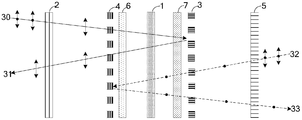
- FIG. 1 is a first structural diagram of a double-sided electroluminescent display panel according to an embodiment of the present disclosure, and a corresponding ambient light path diagram;
- FIG. 2 is a first structural diagram of a double-sided electroluminescent display panel according to an embodiment of the present disclosure, and a corresponding self-illuminating optical path diagram;
- FIG. 3 is a second schematic structural diagram of a double-sided electroluminescent display panel according to an embodiment of the present disclosure, and a corresponding ambient light path diagram;
- FIG. 4 is a second schematic structural diagram of a double-sided electroluminescent display panel according to an embodiment of the present disclosure, and a corresponding self-illuminating optical path diagram;
- FIG. 5 is a schematic diagram of a third structure of a double-sided electroluminescent display panel according to an embodiment of the present disclosure, And a corresponding ambient light path diagram;
- FIG. 6 is a third structural schematic diagram of a double-sided electroluminescent display panel according to an embodiment of the present disclosure, and a corresponding self-illuminating optical path diagram;
- FIG. 7 is a fourth structural diagram of a double-sided electroluminescent display panel according to an embodiment of the present disclosure, and a corresponding ambient light path diagram;
- FIG. 8 is a fourth structural schematic diagram of a double-sided electroluminescent display panel according to an embodiment of the present disclosure, and a corresponding self-illuminating optical path diagram;
- FIG. 9 is a fifth structural diagram of a double-sided electroluminescent display panel according to an embodiment of the present disclosure, and a corresponding ambient light path diagram;
- FIG. 10 is a schematic diagram of a fifth structure of a double-sided electroluminescent display panel according to an embodiment of the present disclosure, and a corresponding self-illuminating optical path diagram;
- FIG. 11 is a sixth structural diagram of a double-sided electroluminescent display panel according to an embodiment of the present disclosure, and a corresponding ambient light path diagram;
- FIG. 12 is a sixth structural diagram of a double-sided electroluminescent display panel according to an embodiment of the present disclosure, and a corresponding self-illuminating optical path diagram.
- Embodiments of the present disclosure provide a double-sided electroluminescent display panel comprising: a double-sided light-emitting transparent electroluminescence (EL) structure, a first absorption polarization structure disposed on a first light-emitting surface of the transparent EL structure, and a first reflective polarization structure disposed on a second illuminating surface of the transparent EL structure (the "upper" relationship described herein includes direct contact and indirect contact); wherein the first absorbing polarization structure and the first reflective polarization structure The transmission axes are perpendicular to each other;
- EL transparent electroluminescence
- a first absorption polarization structure for absorbing light of the first wave component and light of the second wave component
- a first reflective polarization structure for transmitting light of the first wave component and light reflecting the second wave component.
- light herein includes self-luminous of ambient light and EL structure.
- the double-sided electroluminescence display panel provided by the embodiment of the present disclosure, by providing the first absorption polarization structure and the second reflection polarization structure in the double-sided electroluminescence display panel, it is possible to ensure high self-luminescence of the EL structure.
- the rate the intensity of the ambient light is weakened, the ambient light does not penetrate the entire display panel, the contrast of the double-sided electroluminescent display panel is improved, the influence of the ambient light on the double-sided electroluminescent display panel is reduced, and the original
- the double-sided electroluminescent display panel has a problem of low contrast due to transparency of the EL structure.
- the second wave component is a longitudinal wave (P wave) component; or, when the first wave component is a longitudinal wave (P wave) component, the second wave The component is a transverse wave (S wave) component.
- the double-sided electroluminescent display panel provided by the embodiment of the present disclosure includes: a double-sided light-emitting transparent EL structure 1 disposed on the first light-emitting surface of the transparent EL structure 1
- the polarization structure 2 is absorbed, and the first reflective polarization structure 3 is disposed on the second light-emitting surface of the transparent EL structure 1; the transmission axes of the first absorption polarization structure 2 and the first reflection polarization structure 3 are perpendicular to each other.
- the ambient light 01 (light intensity I) incident toward the first light-emitting surface passes through the first absorption polarization structure 2, and the first absorption polarization structure 2 absorbs the ambient light of the S-wave component, and transmits The ambient light of the P wave component, and therefore the ambient light of the P wave component (the light intensity is I/2) passes through the EL structure 1, is reflected by the first reflective polarization structure 3, and passes through the EL structure 1 and the first absorption polarization structure 2 in turn. And emitted, at this time, the outgoing light that is directed in the direction of the first light-emitting surface along the second light-emitting surface contains the ambient light 02 of the P-wave component (the light intensity is I/2).
- the ambient light 03 (light intensity I) incident toward the second light emitting surface first passes through the first reflective polarization structure 3, the first reflective polarization structure 3 transmits the ambient light of the S wave component, reflects the ambient light of the P wave component, and then S The ambient light of the wave component sequentially passes through the EL structure 1 and the first absorption polarization structure 2, since the first absorption polarization structure 2 absorbs the ambient light of the S wave component, the ambient light of the S wave component is not emitted; and the environment of the P wave component The light is directly emitted, and the outgoing light in the direction in which the first light emitting surface is directed to the second light emitting surface at this time includes the ambient light 04 of the P wave component (the light intensity is I/2).
- the ambient light does not penetrate the entire double-sided electroluminescent display panel, and finally the direction along the first illuminating surface pointing to the second illuminating surface
- the intensity of the light emitted and the outgoing light directed in the direction of the first light emitting surface along the second light emitting surface The light intensity is I/2.
- the self-luminous 05 (light intensity I) emitted from the first light-emitting surface in the EL structure 1 passes through the first absorption polarization structure 2, and the self-luminescence of the S-wave component is absorbed by the first absorption polarization structure 2.
- the self-luminous light of the P-wave component is transmitted, so that the self-luminous light of the P-wave component is directly emitted.
- the outgoing light that is directed to the first light-emitting surface along the second light-emitting surface includes the self-luminous light of the P-wave component (the light intensity is I). /2).
- the self-luminous 07 (light intensity I) emitted from the second light-emitting surface in the EL structure 1 passes through the first reflective polarization structure 3, and the self-luminescence of the P-wave component is reflected by the first reflective polarization structure 3 transmitting the S-wave component.
- the self-illumination of the P-wave component sequentially passes through the EL structure 1 and the first absorption polarization structure 2, and the emitted light that is directed in the direction of the first light-emitting surface along the second light-emitting surface contains the self-luminous 08 of the P-wave component ( The light intensity is I/2); and the self-luminescence of the S-wave component is directly emitted, and the outgoing light in the direction of the first light-emitting surface pointing to the second light-emitting surface at this time includes the self-luminous light of the S-wave component (the light intensity is I/) 2).
- the S-wave component of the self-luminous emission will be emitted from one side
- the P-wave component will be emitted from the other side
- the second illumination is directed along the first illumination surface.
- the light intensity of the outgoing light in the direction of the surface is I/2
- the light intensity of the outgoing light in the direction of the second light emitting surface directed to the first light emitting surface is I.
- the emission intensity of the self-luminous light is higher than that of the ambient light, so that the contrast of the double-sided electroluminescent display panel can be improved.
- the double-sided electroluminescent display panel may further include: a second reflection disposed between the first absorption polarization structure and the transparent electroluminescence structure a polarization structure, and a second absorption polarization structure disposed on a side of the first reflective polarization structure away from the transparent EL structure; wherein the transmission axis of the second reflection polarization structure and the second absorption polarization structure are perpendicular to each other.
- the directions of the transmission axes of the first absorption polarization structure and the second reflection polarization structure are the same.
- a second absorption polarization structure for absorbing light of the second wave component and light transmitting the first wave component
- a second reflective polarization structure for transmitting light of the second wave component and light reflecting the first wave component.
- the double-sided electroluminescent display panel may further include: a second reflective polarization disposed between the first absorption polarization structure 2 and the transparent electroluminescent structure 1 .
- Structure 4 and disposed on the side of the first reflective polarization structure 3 away from the transparent EL structure 1
- the second absorption polarization structure 5 wherein the transmission axes of the second reflection polarization structure 4 and the second absorption polarization structure 5 are perpendicular to each other.
- the directions of the transmission axes of the first absorption polarization structure 2 and the second reflection polarization structure 4 are the same.
- the ambient light 10 (light intensity I) incident toward the first light-emitting surface passes through the first absorption polarization structure 2 first, and the first absorption polarization structure 2 absorbs the ambient light of the S-wave component, and transmits The ambient light of the P wave component, and therefore the ambient light of the P wave component (the light intensity is I/2) passes through the second reflective polarization structure 4 and the EL structure 1 in turn, is reflected by the first reflective polarization structure 3, and passes through the EL structure again. 1.
- the second reflective polarization structure 4 and the first absorption polarization structure 2 are emitted together, and the outgoing light that is directed in the direction of the first light-emitting surface along the second light-emitting surface contains the ambient light 11 of the P-wave component (the light intensity is I/ 2).
- the ambient light 12 (light intensity I) incident toward the second light emitting surface first passes through the second absorption polarization structure 5, and since the second absorption polarization structure 5 absorbs the ambient light of the P wave component, the ambient light of the S wave component is transmitted, thus The ambient light of the S-wave component (the light intensity is I/2) passes through the first reflective polarization structure 3 and the EL structure 1 in turn, is reflected by the second reflective polarization structure 4, and passes through the EL structure 1 and the first reflective polarization structure 3 in sequence.
- the second absorption polarization structure 5 is emitted, and the outgoing light in the direction in which the first light-emitting surface is directed to the second light-emitting surface at this time includes the ambient light 13 of the S-wave component (the light intensity is I/2).
- the self-luminous light 14 (light intensity I) emitted from the first light-emitting surface in the EL structure 1 passes through the second reflective polarization structure 4, and the self-luminous light of the P-wave component is transmitted by the second reflective polarization structure 4.
- the self-luminous of the S-wave component is reflected, so that the self-luminous light of the P-wave component is directly emitted through the first absorption polarization structure 2, and the emitted light that is directed to the first light-emitting surface along the second light-emitting surface contains the P-wave component.
- Illumination 15 (light intensity is I/2); and self-luminescence of the S-wave component sequentially passes through the EL structure 1, the first reflective polarization structure 3, and the second absorption polarization structure 5, and is emitted along the first light-emitting surface.
- the outgoing light in the direction of the two light-emitting surfaces contains the self-luminous light 16 of the S-wave component (the light intensity is I/2).
- the self-luminous light 17 (light intensity I) emitted from the second light-emitting surface in the EL structure 1 passes through the first reflective polarization structure 3, and the self-luminescence of the P-wave component is reflected by the first reflective polarization structure 3 transmitting the S-wave component.
- the self-luminous light of the S wave component is directly emitted through the second absorption polarization structure 5, at this time
- the emitted light along the direction in which the first light emitting surface is directed to the second light emitting surface includes the self-luminous light 19 of the S wave component (the light intensity is I/2); and the self-lighting of the P wave component sequentially passes through the EL structure 1 and the second reflective polarization
- the structure 4 and the first absorption polarization structure 2 are emitted, and at this time, the outgoing light directed in the direction of the first light-emitting surface along the second light-emitting surface contains the self-luminous light 18 of the P-wave component (the light intensity is I/2).
- the self-luminous S wave component will be emitted from one side, and the P wave component will be from another
- the light intensity of the outgoing light in the direction in which the first light emitting surface is directed to the second light emitting surface and the light intensity of the outgoing light in the direction in which the second light emitting surface is directed to the first light emitting surface are both I.
- the emission intensity of the self-luminous light is higher than that of the ambient light, which can ensure the intensity of the ambient light under the high emission rate of the self-luminous light of the double-sided structure of the EL structure, thereby improving the contrast of the double-sided display panel. Reduces the impact of ambient light on the double-sided display panel.
- the double-sided electroluminescent display panel may further include: a first absorption polarization structure and a first A first light absorbing structure between the reflective polarizing structures; the first light absorbing structure can be used to attenuate light intensity of light transmitted through the first light absorbing structure.
- the first light absorbing structure may be specifically located between the first absorbing polarization structure and the second reflective polarization structure; or The first light absorbing structure may specifically be located between the second reflective polarizing structure and the transparent EL structure.
- the double-sided electroluminescent display panel may further include: being disposed at the second reflective polarization A second light absorbing structure between the structure and the second absorbing polarizing structure; the second light absorbing structure can be used to attenuate light intensity of light transmitted through the second light absorbing structure.
- the second light absorbing structure may be located between the second absorbing polarization structure and the first reflective polarization structure; or the second light absorbing structure may be specifically located Between the first reflective polarization structure and the transparent EL structure.
- the first light absorbing structure 6 is disposed on the first absorbing polarization structure 2 and the second reflective polarization structure 4 .
- a second light absorbing structure 7 is disposed between the first reflective polarizing structure 3 and the second absorbing polarizing structure 5; assuming that the light transmittance of the first light absorbing structure 6 and the second light absorbing structure 7 are both T;
- the ambient light 20 (light intensity I) incident toward the first light-emitting surface passes through the first absorption polarization structure 2 first, and the first absorption polarization structure 2 absorbs the ambient light of the S-wave component, and transmits The ambient light of the P wave component, so the ambient light of the P wave component (the light intensity is I/2) first passes through the first light absorbing structure 6, and the intensity of the ambient light of the P wave component becomes I*T/2; Then, the second reflective polarization structure 4 and the EL structure 1 are sequentially reflected by the first reflective polarization structure 3, and sequentially passed through the EL structure 1, the first light absorbing structure 6, the second reflective polarization structure 4, and the first absorption polarization structure. 2 and emitted, at this time, the outgoing light directed in the direction of the first light-emitting surface along the second light-emitting surface contains the ambient light 21 of the P-wave component (the light intensity is I*T 2 /2).
- the ambient light 22 (light intensity I) incident toward the second light emitting surface first passes through the second absorption polarization structure 5, and since the second absorption polarization structure 5 absorbs the ambient light of the P wave component, the ambient light of the S wave component is transmitted, thus The ambient light of the S-wave component (the light intensity is I/2) first passes through the second light absorbing structure 7, and the intensity of the ambient light of the S-wave component becomes I*T/2; then the first reflective polarization structure is sequentially passed.
- the outgoing light in the direction in which the first light-emitting surface is directed to the second light-emitting surface contains the ambient light 23 of the S-wave component (the light intensity is I*T 2 /2).
- the ambient light Does not penetrate the entire double-sided electroluminescent display panel, and finally the light intensity of the outgoing light along the direction in which the first light emitting surface is directed to the second light emitting surface and the outgoing light directed in the direction of the first light emitting surface along the second light emitting surface
- the self-luminous light 24 (light intensity I) emitted from the first light-emitting surface in the EL structure 1 passes through the second reflective polarization structure 4, and the self-luminous light of the P-wave component is transmitted by the second reflective polarization structure 4.
- the self-luminous of the S-wave component is reflected, so that the self-illumination of the P-wave component is sequentially emitted through the first light-absorbing structure 6 and the first absorption-polarization structure 2, and the direction along the second light-emitting surface is directed to the first light-emitting surface.
- the emitted light includes a self-luminous 25 of a P-wave component (light intensity is I*T/2); and the self-illumination of the S-wave component sequentially passes through the EL structure 1, the first reflective polarization structure 3, the second light absorbing structure 7, and the second Absorbing the polarizing structure 5 and emitting it, at this time, along the direction in which the first light emitting surface is directed to the second light emitting surface
- the emitted light contains self-luminous light 26 of the S-wave component (light intensity is I*T/2).
- the self-luminous 27 (light intensity I) emitted from the second light-emitting surface in the EL structure 1 passes through the first reflective polarization structure 3, and the self-luminescence of the P-wave component is reflected by the first reflective polarization structure 3 transmitting the self-luminescence of the S-wave component Therefore, the self-illumination of the S-wave component is sequentially emitted through the second light-absorbing structure 7 and the second absorption-polarization structure 5, and the outgoing light that is directed to the second light-emitting surface along the first light-emitting surface includes the S-wave component.
- Luminescence 29 (light intensity is I*T/2); and self-luminescence of the P wave component sequentially passes through the EL structure 1, the second reflective polarization structure 4, the first light absorbing structure 6, and the first absorption polarization structure 2, and is emitted.
- the outgoing light in the direction in which the second light emitting surface is directed to the first light emitting surface includes the self-luminous light 28 of the P wave component (the light intensity is I*T/2).
- the first absorption polarization structure 2 the first reflection polarization structure 3, the second absorption polarization structure 5, the second reflection polarization structure 4, the first light absorption structure 6, and the second light absorption structure 7, self-luminescence
- the S wave component is emitted from one side
- the P wave component is emitted from the other side
- the light intensity of the outgoing light in the direction of the first light emitting surface pointing to the second light emitting surface and the first light emitting surface along the second light emitting surface
- the emission intensity of self-luminous is higher than that of ambient light, which can greatly weaken the intensity of ambient light while ensuring high emission rate of self-luminescence on both sides of the EL structure, and ambient light does not penetrate the entire display.
- the panel further improves the contrast of the double-sided display panel, greatly reduces the influence of ambient light on the double-sided display panel, and improves the problem that the original double-sided electroluminescent display panel has low contrast due to transparency of the EL structure.
- the first light absorbing structure 6 is disposed between the second reflective polarizing structure 4 and the transparent EL structure 1 .
- the second light absorbing structure 7 is disposed between the first reflective polarizing structure 3 and the transparent EL structure 1; it is assumed that the light transmittances of the first light absorbing structure 6 and the second light absorbing structure 7 are both T.
- the ambient light 30 (the light intensity is I) incident toward the first light-emitting surface passes through the first absorption polarization structure 2, and the first absorption polarization structure 2 absorbs the ambient light of the S-wave component, and transmits The ambient light of the P wave component, and therefore the ambient light of the P wave component (the light intensity is I/2) sequentially passes through the second reflective polarization structure 4 and the first light absorbing structure 6, and the intensity of the ambient light of the P wave component changes at this time.
- the outgoing light in the direction of the plane contains ambient light 31 of the P-wave component (light intensity is I*T 4 /2).
- the ambient light of the S-wave component (the light intensity is I/2) sequentially passes through the first reflective polarization structure 3 and the second light-absorbing structure 7, and the intensity of the ambient light of the S-wave component becomes I*T/2; Passing through the EL structure 1 and the first light absorbing structure 6 in sequence, at this time, the intensity of the ambient light of the S wave component becomes I*T 2 /2; the second reflective polarization structure 4 reflects, and then passes through the first light absorption again.
- the structure 6, the EL structure 1, the second light absorbing structure 7, the first reflective polarization structure 3, and the second absorbing polarization structure 5 are emitted, and the outgoing light directed in the direction of the second light emitting surface along the first light emitting surface includes S Ambient light 33 of the wave component (light intensity is I*T 4 /2).
- the ambient light Does not penetrate the entire double-sided electroluminescent display panel, and finally the light intensity of the outgoing light along the direction in which the first light emitting surface is directed to the second light emitting surface and the outgoing light directed in the direction of the first light emitting surface along the second light emitting surface
- the self-luminous light 34 (light intensity I) emitted from the first light-emitting surface in the EL structure 1 sequentially passes through the first light absorbing structure 6 and the second reflective polarization structure 4, due to the second reflective polarization structure.
- the emitted light includes a self-luminous 35 of a P-wave component (light intensity is I*T/2); and the self-illumination of the S-wave component sequentially passes through the first light absorbing layer 6, the EL structure 1, the second light absorbing structure 7, and the first
- the reflective polarization structure 3 and the second absorption polarization structure 5 are emitted, and the outgoing light in the direction of the first light emitting surface pointing to the second light emitting surface at this time includes the self-luminous light 36 of the S wave component (the light intensity is I*T 3 /2) ).
- the self-luminous light of the P wave component is reflected, so that the self-luminous light of the S wave component is directly emitted through the second absorption polarization structure 5, and the outgoing light that is directed to the second light emitting surface along the first light emitting surface includes the S wave component.
- Illumination 39 (light intensity is I*T/2); and self-luminescence of the P wave component sequentially passes through the second light absorbing structure 7, the EL structure 1, the first light absorbing structure 6, the second reflective polarization structure 4, and the first absorption
- the polarization structure 2 is emitted, and the emitted light in the direction in which the second light-emitting surface is directed to the first light-emitting surface at this time includes the self-luminous light 38 of the P-wave component (the light intensity is I*T 3 /2).
- the first absorption polarization structure 2 the first reflection polarization structure 3, the second absorption polarization structure 5, the second reflection polarization structure 4, the first light absorption structure 6, and the second light absorption structure 7, self-luminescence
- the S wave component is emitted from one side
- the P wave component is emitted from the other side
- the light intensity of the outgoing light in the direction of the first light emitting surface pointing to the second light emitting surface and the first light emitting surface along the second light emitting surface
- the emission intensity of self-luminous is higher than that of ambient light, which can greatly weaken the intensity of ambient light while ensuring high emission rate of self-luminescence on both sides of the EL structure, and ambient light does not penetrate the entire display.
- the panel further improves the contrast of the double-sided display panel, greatly reduces the influence of ambient light on the double-sided display panel, and improves the problem that the original double-sided electroluminescent display panel has low contrast due to transparency of the EL structure.
- the structure of the above-mentioned double-sided electroluminescent display panel includes not only the structure described above, but also various other structures, such as having only the first absorption polarization structure 2, the first reflection polarization structure 3, and a first light absorbing structure 6; or, having only the first absorbing polarization structure 2, the first reflective polarization structure 3, the first light absorbing structure 6, and the second light absorbing structure 7; or, having only the first absorbing polarization structure 2 a first reflective polarization structure 3, a second absorption polarization structure 5, a second reflective polarization structure 4, and a first light absorption structure 6; or, only having a first absorption polarization structure 2, a first reflection polarization structure 3, and a second absorption polarization
- the structure 5, the second reflective polarization structure 4, the second light absorbing structure 7, and the like are not limited as long as the contrast of the double-sided display panel can be improved.
- the double-sided electroluminescence display panel has only the first absorption polarization structure 2, the first reflection polarization structure 3, the first light absorption structure 6, and the second light absorption structure 7 as an example, and the following detailed description of the optical path diagram is performed:
- the first light absorbing structure 6 is located between the first absorbing polarization structure 2 and the EL structure 1, and the second light The absorbing structure 7 is located between the EL structure 1 and the first reflective polarizing structure 3.
- the ambient light 40 (light intensity I) incident toward the first light-emitting surface passes through the first absorption polarization structure 2 first, and the first absorption polarization structure 2 absorbs the ambient light of the S-wave component, and transmits The ambient light of the P wave component, and therefore the ambient light of the P wave component (the light intensity is I/2) sequentially passes through the first light absorbing layer 6, the EL structure 1 and the second light absorbing layer 7, and the ambient light of the P wave component at this time
- the intensity of the light becomes I*T 2 /2; is reflected by the first reflective polarization structure 3, and passes through the second light absorbing layer 7, the EL structure 1, the first light absorbing layer 6, and the first absorbing polarization structure 2 in turn.
- the emitted light in the direction in which the second light emitting surface is directed to the first light emitting surface at this time includes the ambient light 41 of the P wave component (the light intensity is I*T 4 /2).
- the ambient light 42 (light intensity I) incident toward the second light emitting surface first passes through the first reflective polarization structure 3, the first reflective polarization structure 3 transmits the ambient light of the S wave component, reflects the ambient light of the P wave component, and then S The ambient light of the wave component passes through the second light absorbing structure 7, the EL structure 1, the first light absorbing structure 6, and the first absorbing polarization structure 2 in order, since the first absorbing polarization structure 2 absorbs the ambient light of the S wave component, so S The ambient light of the wave component is not emitted; and the ambient light of the P wave component is directly emitted. At this time, the outgoing light that is directed to the second light emitting surface along the first light emitting surface contains the ambient light 43 of the P wave component (the light intensity is I/). 2).
- the ambient light does not penetrate the entire double-sided electroluminescent display panel, and finally the light intensity of the emitted light along a first light emitting surface light emitting surface of the pointing direction of the second I / 2, the second light emitting surface directed along the direction of the first light emitting surface of the light intensity of the emitted light is I * T 4/2 .
- the self-luminous light 44 (light intensity I) emitted from the first light-emitting surface in the EL structure 1 sequentially passes through the first light-absorbing structure 6 and the first absorption polarization structure 2, due to the first absorption polarization structure. 2 absorbing the self-luminous of the S-wave component and transmitting the self-luminous of the P-wave component, so that the self-luminescence of the P-wave component is directly emitted, and the outgoing light that is directed in the direction of the first light-emitting surface along the second light-emitting surface contains the P-wave component.
- Self-illuminating 45 (light intensity is I*T/2).
- the emitted light of the second light emitting surface pointing in the direction of the first light emitting surface includes the self-luminous light 47 of the P wave component (the light intensity is I*T 3 /2); and the self-luminous light of the S wave component is directly emitted, and the first light is emitted along the first light emitting surface.
- the outgoing light whose direction is directed to the second light-emitting surface contains the self-luminous light 48 of the S-wave component (the light
- the self-luminous S wave component will be emitted from one side, and the P wave component will be The other side exits, and finally, the intensity of the outgoing light in the direction in which the first light emitting surface is directed to the second light emitting surface is I*T/2, and the light intensity of the outgoing light in the direction of the second light emitting surface pointing to the first light emitting surface Is I*(T 4 +T)/2.
- the emission intensity of the self-luminous light is higher than that of the ambient light, especially the intensity of the emitted light along the direction in which the second light-emitting surface is directed to the first light-emitting surface is high, so that the double-sided electroluminescent display panel can be improved. Contrast.
- the first light absorbing structure 6 is located between the first absorbing polarization structure 2 and the EL structure 1 ,
- the second light absorbing structure 7 is located on a side of the first reflective polarization structure 3 away from the EL structure 1;
- the ambient light 49 (light intensity I) incident toward the first light-emitting surface passes through the first absorption polarization structure 2 first, and the first absorption polarization structure 2 absorbs the ambient light of the S-wave component, and transmits The ambient light of the P wave component, and therefore the ambient light of the P wave component (the light intensity is I/2) sequentially passes through the first light absorbing layer 6 and the EL structure 1, and the intensity of the ambient light of the P wave component becomes I* at this time.
- the outgoing light in the direction includes the ambient light 50 of the P-wave component (the light intensity is I*T 2 /2).
- the ambient light 51 (light intensity I) incident toward the second light emitting surface sequentially passes through the second light absorbing structure 7 and the first reflective polarization structure 3, and the first reflective polarization structure 3 transmits ambient light of the S wave component, and reflects the P wave.
- the ambient light of the component, and then the ambient light of the S-wave component sequentially passes through the EL structure 1, the first light absorbing structure 6, and the first absorbing polarization structure 2, since the first absorbing polarization structure 2 absorbs the ambient light of the S-wave component, so S
- the ambient light of the wave component is not emitted; and the ambient light of the P wave component is directly emitted through the second light absorbing structure 7.
- the outgoing light that is directed to the second light emitting surface along the first light emitting surface contains ambient light of the P wave component.
- 52 light intensity is I*T 2 /2).
- the ambient light does not penetrate the entire double-sided electroluminescent display panel, and finally
- the light intensity of the outgoing light in the direction in which the first light emitting surface is directed to the second light emitting surface and the light intensity of the outgoing light in the direction in which the second light emitting surface is directed to the first light emitting surface are both I*T 2 /2.
- the self-luminous light 53 (light intensity I) emitted from the first light-emitting surface in the EL structure 1 sequentially passes through the first light absorbing structure 6 and the first absorption polarization structure 2, due to the first absorption polarization structure. 2 absorbing the self-luminous of the S-wave component and transmitting the self-luminous of the P-wave component, so that the self-luminescence of the P-wave component is directly emitted, and the outgoing light that is directed in the direction of the first light-emitting surface along the second light-emitting surface contains the P-wave component.
- Self-illumination 54 (light intensity is I*T/2).
- the self-luminous 55 (light intensity I) emitted from the second light-emitting surface in the EL structure 1 passes through the first reflective polarization structure 3, and the self-luminescence of the P-wave component is reflected by the first reflective polarization structure 3 transmitting the S-wave component. Therefore, the self-luminous light of the P wave component sequentially passes through the EL structure 1, the first light absorbing structure 6, and the first absorbing polarization structure 2, and the emitted light that is directed in the direction of the first light emitting surface along the second light emitting surface includes P.
- Self-illumination 56 of the wave component (light intensity is I*T/2); and self-luminescence of the S-wave component is directly emitted through the second light absorbing structure 7, at this time along the direction of the first light-emitting surface pointing to the second light-emitting surface
- the emitted light contains self-luminous light 57 of the S-wave component (light intensity is I*T/2).
- the self-luminous S wave component will be emitted from one side, and the P wave component will be The other side is emitted, and finally, the light intensity of the outgoing light in the direction in which the first light emitting surface is directed to the second light emitting surface is I*T, and the light intensity of the outgoing light in the direction in which the second light emitting surface is directed to the first light emitting surface is I *T/2.
- the emission intensity of the self-luminous light is much higher than that of the ambient light, so that the contrast of the double-sided electroluminescent display panel can be improved.
- the first reflective polarizing structure or the second reflective polarizing structure may be configured as a metal wire grid polarizer or a reflective polarizer.
- the reflective polarizer can select a 3M reflective polarizer DBEF.
- the selection of the first reflective polarization structure or the second reflective polarization structure may be determined according to actual conditions, and is not limited herein.
- the first absorption polarization structure or the second absorption polarization structure is a linear polarization plate.
- the linear polarizing plate may specifically include a first triacetate film (TAC), a polyvinyl alcohol film (PVA), and a second triacetate film (TAC) which are laminated, that is, by laminating a TAC protective film on the PVA film.
- a linear polarizing plate obtained on the surface and the lower surface.
- the selection of the first absorbing polarization structure or the second absorbing polarization structure may be determined according to actual conditions, and is not limited herein.
- the material of the receiving structure may be an organic resin material containing a dye; the material of the second light absorbing structure may also be an organic resin material containing a dye; the dye may serve as a light absorbing agent.
- the material of the first light absorbing structure or the second light absorbing structure may be determined according to actual conditions, and is not limited herein.
- the EL structure in the double-sided electroluminescent display panel provided by the embodiment of the present disclosure generally has other film layer structures such as a light-emitting layer, a cathode, and an anode, and a thin film transistor is generally formed on the substrate.
- Structures such as a gate line and a data line may be implemented in various manners, and are not limited herein.
- each of the absorption polarization structure, the reflective polarization structure, and the light absorption structure may be disposed in parallel to the first light-emitting surface or the second light-emitting surface.
- each of the absorption polarization structure, the reflective polarization structure, and the light absorption structure may cover the respective first first light emitting surface and second light emitting surface.
- an embodiment of the present disclosure further provides a display device, including the double-sided electroluminescent display panel provided by the embodiment of the present disclosure, which may be: a mobile phone, a tablet computer, a television, a display, a notebook. Any product or component that has a display function, such as a computer, digital photo frame, and navigator. Other indispensable components of the display device are understood by those skilled in the art, and are not described herein, nor should they be construed as limiting the disclosure. For the implementation of the display device, reference may be made to the embodiment of the double-sided electroluminescent display panel described above, and the repeated description is omitted.
- a double-sided electroluminescent display panel and a display device include: a double-sided light-emitting transparent electroluminescent structure, and a first absorption polarization structure disposed on a first light-emitting surface of the transparent electroluminescent structure And a first reflective polarization structure disposed on the second illuminating surface of the transparent electroluminescent structure; wherein the transmission axes of the first absorbing polarization structure and the first reflective polarization structure are perpendicular to each other; and the first absorbing polarization structure for absorbing Light of a first wave component and light of a second wave component; a first reflective polarization structure for transmitting light of the first wave component and light of the second wave component.
- the intensity of the ambient light can be weakened while ensuring a high emission rate of self-luminescence of the electroluminescence device, ambient light It does not penetrate the entire display panel, improves the contrast of the double-sided display panel, reduces the influence of ambient light on the double-sided display panel, and improves the low contrast of the original double-sided display panel due to the transparency of the electroluminescent structure.
Landscapes
- Physics & Mathematics (AREA)
- Optics & Photonics (AREA)
- Electroluminescent Light Sources (AREA)
Abstract
提供了一种双面电致发光显示面板及显示装置。该双面电致发光显示面板包括:设置在透明EL结构(1)的第一发光面上的第一吸收偏振结构(2),以及设置在EL结构(1)的第二发光面上的第一反射偏振结构(3);其中,第一吸收偏振结构(2)和第一反射偏振结构(3)的透射轴互相垂直;第一吸收偏振结构(2)被配置为吸收第一波分量的光和透射第二波分量的光;第一反射偏振结构(3)被配置为透射第一波分量的光和反射第二波分量的光。通过第一吸收偏振结构和第一反射偏振结构的共同作用,可以在保证自发光的高出射率情况下削弱环境光的强度,改善了原有双面显示面板因EL结构透明导致对比度低的问题。
Description
本公开涉及一种双面电致发光显示面板及显示装置。
目前,有机发光二极管(Organic Light-Emitting Diode,OLED)显示装置因具有自发光、不需要背光源模块、重量轻、厚度薄、构造简单、耐用等应用优势,备受产业界的关注。
OLED器件有非透明和透明两种,非透明的OLED器件仅能一面发光,因此在制备双面OLED显示装置时,需要两个独立显示装置贴合,或者需要对分别设置OLED器件的基板进行密封,因此采用非透明的OLED器件制备双面OLED显示装置的成本较高,且双面OLED显示装置厚度较厚。而透明OLED器件可以进行双面发光,双面OLED显示面板要求电致发光(Electroluminescent,EL)器件的阳极和阴极都有较高的透过率,阳极一般用ITO制作,阴极可以用IZO或者Mg/Ag(9:1厚度),EL器件自发光就可以双向出射,实现双面显示OLED器件。但是由于EL器件是透明的,环境光也可以穿透OLED面板与EL器件自发光一起出射,致使OLED器件对比度大大降低,使用者的观看效果非常容易受到环境光的影响。
因此,如何提高双面OLED显示器的对比度,是本领域技术人员亟待解决的技术问题。
发明内容
本公开实施例提供了一种双面电致发光显示面板,包括:双面发光的透明电致发光结构,设置在所述透明电致发光结构的第一发光面上的第一吸收偏振结构,以及设置在所述透明电致发光结构的第二发光面上的第一反射偏振结构;其中,所述第一吸收偏振结构和第一反射偏振结构的透射轴互相垂直;所述第一吸收偏振结构被配置为吸收第一波分量的光和透射第二波分量的光;所述第一反射偏振结构被配置为透射第一波分量的光和反射第二波分
量的光。
在一些示例中,在本公开实施例提供的上述双面电致发光显示面板中,还包括:设置在所述第一吸收偏振结构和所述透明电致发光结构之间的第二反射偏振结构,以及设置在所述第一反射偏振结构的远离所述透明电致发光结构一侧的第二吸收偏振结构;其中,所述第二反射偏振结构与所述第二吸收偏振结构的透射轴互相垂直,所述第一吸收偏振结构和所述第二反射偏振结构的透射轴的方向相同;所述第二吸收偏振结构被配置为吸收第二波分量的光和透射第一波分量的光;所述第二反射偏振结构被配置为透射第二波分量的光和反射第一波分量的光。
在一些示例中,在本公开实施例提供的上述双面电致发光显示面板中,还包括:设置在所述第一吸收偏振结构和第一反射偏振结构之间的第一光吸收结构;所述第一光吸收结构,用于减弱透过所述第一光吸收结构的光的光强。
在一些示例中,在本公开实施例提供的上述双面电致发光显示面板中,所述第一光吸收结构位于所述第一吸收偏振结构和第二反射偏振结构之间;或,所述第一光吸收结构位于所述第二反射偏振结构和透明电致发光结构之间。
在一些示例中,在本公开实施例提供的上述双面电致发光显示面板中,还包括:设置在所述第二反射偏振结构和第二吸收偏振结构之间的第二光吸收结构;所述第二光吸收结构被配置为减弱透过所述第二光吸收结构的光的光强。
在一些示例中,在本公开实施例提供的上述双面电致发光显示面板中,所述第二光吸收结构位于所述第二吸收偏振结构和第一反射偏振结构之间;或,所述第二光吸收结构位于所述第一反射偏振结构和透明电致发光结构之间。
在一些示例中,在本公开实施例提供的上述双面电致发光显示面板中,所述第一波分量为横波分量,第二波分量为纵波分量;或,所述第一波分量为纵波分量,第二波分量为横波分量。
在一些示例中,在本公开实施例提供的上述双面电致发光显示面板中,所述第一反射偏振结构或第二反射偏振结构为金属线栅偏振器或反射型偏光
片。
在一些示例中,在本公开实施例提供的上述双面电致发光显示面板中,所述第一吸收偏振结构或第二吸收偏振结构为线偏振片。
在一些示例中,在本公开实施例提供的上述双面电致发光显示面板中,所述线偏振片包括层叠设置的第一三醋酸纤维薄膜、聚乙烯醇薄膜和第二三醋酸纤维薄膜。
在一些示例中,在本公开实施例提供的上述双面电致发光显示面板中,所述第一光吸收结构的材料为包含染料的有机树脂材料。
在一些示例中,在本公开实施例提供的上述双面电致发光显示面板中,所述第二光吸收结构的材料为包含染料的有机树脂材料。
在一些示例中,所述第一吸收偏振结构平行于所述第一发光面,所述第一反射偏振结构平行于所述第二发光面。
在一些示例中,所述第一吸收偏振结构覆盖整个第一发光面,所述第一反射偏振结构覆盖整个第二发光面。
本公开实施例还提供了一种显示装置,包括本公开实施例提供的上述双面电致发光显示面板。
为了更清楚地说明本公开实施例的技术方案,下面将对实施例的附图作简单地介绍,显而易见地,下面描述中的附图仅仅涉及本公开的一些实施例,而非对本公开的限制。
图1为本公开实施例提供的双面电致发光显示面板的第一种结构示意图,以及对应的环境光光路图;
图2为本公开实施例提供的双面电致发光显示面板的第一种结构示意图,以及对应的自发光光路图;
图3为本公开实施例提供的双面电致发光显示面板的第二种结构示意图,以及对应的环境光光路图;
图4为本公开实施例提供的双面电致发光显示面板的第二种结构示意图,以及对应的自发光光路图;
图5为本公开实施例提供的双面电致发光显示面板的第三种结构示意图,
以及对应的环境光光路图;
图6为本公开实施例提供的双面电致发光显示面板的第三种结构示意图,以及对应的自发光光路图;
图7为本公开实施例提供的双面电致发光显示面板的第四种结构示意图,以及对应的环境光光路图;
图8为本公开实施例提供的双面电致发光显示面板的第四种结构示意图,以及对应的自发光光路图;
图9为本公开实施例提供的双面电致发光显示面板的第五种结构示意图,以及对应的环境光光路图;
图10为本公开实施例提供的双面电致发光显示面板的第五种结构示意图,以及对应的自发光光路图;
图11为本公开实施例提供的双面电致发光显示面板的第六种结构示意图,以及对应的环境光光路图;
图12为本公开实施例提供的双面电致发光显示面板的第六种结构示意图,以及对应的自发光光路图。
为使本公开实施例的目的、技术方案和优点更加清楚,下面将结合本公开实施例的附图,对本公开实施例的技术方案进行清楚、完整地描述。显然,所描述的实施例是本公开的一部分实施例,而不是全部的实施例。基于所描述的本公开的实施例,本领域普通技术人员在无需创造性劳动的前提下所获得的所有其他实施例,都属于本公开保护的范围。
附图中各结构的大小和形状不反映双面电致发光显示面板的真实比例,目的只是示意说明本公开内容。
本公开实施例提供了一种双面电致发光显示面板,包括:双面发光的透明电致发光(EL)结构,设置在透明EL结构的第一发光面上的第一吸收偏振结构,以及设置在透明EL结构的第二发光面上的第一反射偏振结构(这里所描述的“上”的关系包括直接接触和非直接接触);其中,第一吸收偏振结构和第一反射偏振结构的透射轴互相垂直;
第一吸收偏振结构,用于吸收第一波分量的光和透射第二波分量的光;
第一反射偏振结构,用于透射第一波分量的光和反射第二波分量的光。
需要说明的是,这里的“光”包括环境光和EL结构的自发光。
在本公开实施例提供的上述双面电致发光显示面板,通过在双面电致发光显示面板中设置第一吸收偏振结构和第二反射偏振结构,可以在保证EL结构的自发光的高出射率情况下削弱环境光的强度,环境光不会穿透整个显示面板,提高了双面电致发光显示面板的对比度,降低了环境光对于双面电致发光显示面板的影响,改善了原有双面电致发光显示面板因EL结构透明导致对比度低的问题。
需要说明的是,当第一波分量为横波(S波)分量时,第二波分量为纵波(P波)分量;或,当第一波分量为纵波(P波)分量时,第二波分量为横波(S波)分量。
例如,以图1和图2为例,本公开实施例提供的双面电致发光显示面板包括:双面发光的透明EL结构1,设置在透明EL结构1的第一发光面上的第一吸收偏振结构2,以及设置在透明EL结构1的第二发光面上的第一反射偏振结构3;第一吸收偏振结构2和第一反射偏振结构3的透射轴互相垂直。
如图1的光路所示,朝着第一发光面入射的环境光01(光强为I)先通过第一吸收偏振结构2,由于第一吸收偏振结构2吸收S波分量的环境光,透射P波分量的环境光,因此P波分量的环境光(光强为I/2)通过EL结构1,经第一反射偏振结构3进行反射,再次依次通过EL结构1和第一吸收偏振结构2并射出,此时沿着第二发光面指向第一发光面的方向的出射光包含P波分量的环境光02(光强为I/2)。
朝着第二发光面入射的环境光03(光强为I)先通过第一反射偏振结构3,第一反射偏振结构3透射S波分量的环境光,反射P波分量的环境光,然后S波分量的环境光依次通过EL结构1和第一吸收偏振结构2,由于第一吸收偏振结构2会吸收S波分量的环境光,因此S波分量的环境光未射出;而P波分量的环境光直接射出,此时沿着第一发光面指向第二发光面的方向的出射光包含P波分量的环境光04(光强为I/2)。
可见,由于第一吸收偏振结构2和第一反射偏振结构3的存在,环境光不会穿透整个双面电致发光显示面板,最终沿着第一发光面指向第二发光面的方向的出射光的光强和沿着第二发光面指向第一发光面的方向的出射光的
光强均为I/2。
如图2的光路所示,EL结构1中从第一发光面出射的自发光05(光强为I)通过第一吸收偏振结构2,由于第一吸收偏振结构2吸收S波分量的自发光,透射P波分量的自发光,因此P波分量的自发光直接射出,此时沿着第二发光面指向第一发光面的方向的出射光包含P波分量的自发光06(光强为I/2)。
EL结构1中从第二发光面出射的自发光07(光强为I)通过第一反射偏振结构3,由于第一反射偏振结构3透射S波分量的自发光,反射P波分量的自发光,因此P波分量的自发光依次通过EL结构1和第一吸收偏振结构2并射出,此时沿着第二发光面指向第一发光面的方向的出射光包含P波分量的自发光08(光强为I/2);而S波分量的自发光直接射出,此时沿着第一发光面指向第二发光面的方向的出射光包含S波分量的自发光06(光强为I/2)。
可见,由于第一吸收偏振结构2和第一反射偏振结构3的存在,自发光的S波分量会从一面射出,P波分量会从另一面出射,最终沿着第一发光面指向第二发光面的方向的出射光的光强为I/2,沿着第二发光面指向第一发光面的方向的出射光的光强为I。
经比较,自发光的出射强度相较于环境光还是较高的,因此可以提高双面电致发光显示面板的对比度。
例如,在本公开实施例提供的上述双面电致发光显示面板中,该双面电致发光显示面板还可以包括:设置在第一吸收偏振结构和透明电致发光结构之间的第二反射偏振结构,以及设置在第一反射偏振结构上远离透明EL结构一侧的第二吸收偏振结构;其中,第二反射偏振结构与第二吸收偏振结构的透射轴互相垂直。例如,第一吸收偏振结构和第二反射偏振结构的透射轴的方向相同。
第二吸收偏振结构,用于吸收第二波分量的光和透射第一波分量的光;
第二反射偏振结构,用于透射第二波分量的光和反射第一波分量的光。
例如,以图3和图4为例,本公开实施例提供的双面电致发光显示面板还可以包括:设置在第一吸收偏振结构2和透明电致发光结构1之间的第二反射偏振结构4,以及设置在第一反射偏振结构3上远离透明EL结构1一侧
的第二吸收偏振结构5;其中,第二反射偏振结构4与第二吸收偏振结构5的透射轴互相垂直。例如,第一吸收偏振结构2和第二反射偏振结构4的透射轴的方向相同。
如图3的光路所示,朝着第一发光面入射的环境光10(光强为I)先通过第一吸收偏振结构2,由于第一吸收偏振结构2吸收S波分量的环境光,透射P波分量的环境光,因此P波分量的环境光(光强为I/2)依次通过第二反射偏振结构4和EL结构1,经第一反射偏振结构3进行反射,再次依次通过EL结构1、第二反射偏振结构4和第一吸收偏振结构2并射出,此时沿着第二发光面指向第一发光面的方向的出射光包含P波分量的环境光11(光强为I/2)。
朝着第二发光面入射的环境光12(光强为I)先通过第二吸收偏振结构5,由于第二吸收偏振结构5吸收P波分量的环境光,透射S波分量的环境光,因此S波分量的环境光(光强为I/2)依次通过第一反射偏振结构3和EL结构1,经第二反射偏振结构4进行反射,再次依次通过EL结构1、第一反射偏振结构3和第二吸收偏振结构5并射出,此时沿着第一发光面指向第二发光面的方向的出射光包含S波分量的环境光13(光强为I/2)。
可见,由于第一吸收偏振结构2、第一反射偏振结构3、第二吸收偏振结构5和第二反射偏振结构4的存在,环境光不会穿透整个双面电致发光显示面板,最终沿着第一发光面指向第二发光面的方向的出射光的光强和沿着第二发光面指向第一发光面的方向的出射光的光强均为I/2。
如图4的光路所示,EL结构1中从第一发光面出射的自发光14(光强为I)通过第二反射偏振结构4,由于第二反射偏振结构4透射P波分量的自发光,反射S波分量的自发光,因此P波分量的自发光通过第一吸收偏振结构2直接射出,此时沿着第二发光面指向第一发光面的方向的出射光包含P波分量的自发光15(光强为I/2);而S波分量的自发光依次通过EL结构1、第一反射偏振结构3和第二吸收偏振结构5并射出,此时沿着第一发光面指向第二发光面的方向的出射光包含S波分量的自发光16(光强为I/2)。
EL结构1中从第二发光面出射的自发光17(光强为I)通过第一反射偏振结构3,由于第一反射偏振结构3透射S波分量的自发光,反射P波分量的自发光,因此S波分量的自发光通过第二吸收偏振结构5直接射出,此时
沿着第一发光面指向第二发光面的方向的出射光包含S波分量的自发光19(光强为I/2);而P波分量的自发光依次通过EL结构1、第二反射偏振结构4和第一吸收偏振结构2并射出,此时沿着第二发光面指向第一发光面的方向的出射光包含P波分量的自发光18(光强为I/2)。
可见,由于第一吸收偏振结构2、第一反射偏振结构3、第二吸收偏振结构5和第二反射偏振结构4的存在,自发光的S波分量会从一面射出,P波分量会从另一面出射,最终沿着第一发光面指向第二发光面的方向的出射光的光强和沿着第二发光面指向第一发光面的方向的出射光的光强均为I。
经比较,自发光的出射强度相较于环境光还是较高的,可以保证EL结构双面的自发光的高出射率情况下削弱环境光的强度,进而提高了双面显示面板的对比度,大大降低了环境光对于双面显示面板的影响。
例如,在本公开实施例提供的上述双面电致发光显示面板中,为了进一步减小环境光的出射率,该双面电致发光显示面板还可以包括:设置在第一吸收偏振结构和第一反射偏振结构之间的第一光吸收结构;该第一光吸收结构可以用于减弱透过第一光吸收结构的光的光强。
较佳地,在具体实施时,在本公开实施例提供的上述双面电致发光显示面板中,第一光吸收结构具体可以位于第一吸收偏振结构和第二反射偏振结构之间;或,第一光吸收结构具体可以位于第二反射偏振结构和透明EL结构之间。
进一步地,例如,在本公开实施例提供的上述双面电致发光显示面板中,为了进一步减小环境光的出射率,该双面电致发光显示面板还可以包括:设置在第二反射偏振结构和第二吸收偏振结构之间的第二光吸收结构;该第二光吸收结构可以用于减弱透过第二光吸收结构的光的光强。
例如,在本公开实施例提供的上述双面电致发光显示面板中,第二光吸收结构可以位于第二吸收偏振结构和第一反射偏振结构之间;或,第二光吸收结构具体可以位于第一反射偏振结构和透明EL结构之间。
具体地,以图5和图6为例,在本公开实施例提供的双面电致发光显示面板中,第一光吸收结构6设置在第一吸收偏振结构2和第二反射偏振结构4之间;以及第二光吸收结构7设置在第一反射偏振结构3和第二吸收偏振结构5之间;假设第一光吸收结构6和第二光吸收结构7的光透过率均为T;
如图5的光路所示,朝着第一发光面入射的环境光20(光强为I)先通过第一吸收偏振结构2,由于第一吸收偏振结构2吸收S波分量的环境光,透射P波分量的环境光,因此P波分量的环境光(光强为I/2)先通过第一光吸收结构6,此时P波分量的环境光的光强变为I*T/2;之后依次通过第二反射偏振结构4和EL结构1,经第一反射偏振结构3进行反射,再次依次通过EL结构1、第一光吸收结构6、第二反射偏振结构4和第一吸收偏振结构2并射出,此时沿着第二发光面指向第一发光面的方向的出射光包含P波分量的环境光21(光强为I*T2/2)。
朝着第二发光面入射的环境光22(光强为I)先通过第二吸收偏振结构5,由于第二吸收偏振结构5吸收P波分量的环境光,透射S波分量的环境光,因此S波分量的环境光(光强为I/2)先通过第二光吸收结构7,此时S波分量的环境光的光强变为I*T/2;之后依次通过第一反射偏振结构3和EL结构1,经第二反射偏振结构4进行反射,再次依次通过EL结构1、第一反射偏振结构3、第二光吸收结构7和第二吸收偏振结构5并射出,此时沿着第一发光面指向第二发光面的方向的出射光包含S波分量的环境光23(光强为I*T2/2)。
可见,由于上述第一吸收偏振结构2、第一反射偏振结构3、第二吸收偏振结构5、第二反射偏振结构4、第一光吸收结构6和第二光吸收结构7的存在,环境光不会穿透整个双面电致发光显示面板,最终沿着第一发光面指向第二发光面的方向的出射光的光强和沿着第二发光面指向第一发光面的方向的出射光的光强均为I*T2/2。若T=0.8,则出射光的光强均为0.32I;若T=0.7,则出射光的光强均为0.245I,环境光的强度得到较大削弱,使用者也不易受到环境光的影响。
如图6的光路所示,EL结构1中从第一发光面出射的自发光24(光强为I)通过第二反射偏振结构4,由于第二反射偏振结构4透射P波分量的自发光,反射S波分量的自发光,因此P波分量的自发光依次通过第一光吸收结构6和第一吸收偏振结构2直接射出,此时沿着第二发光面指向第一发光面的方向的出射光包含P波分量的自发光25(光强为I*T/2);而S波分量的自发光依次通过EL结构1、第一反射偏振结构3、第二光吸收结构7和第二吸收偏振结构5并射出,此时沿着第一发光面指向第二发光面的方向的出
射光包含S波分量的自发光26(光强为I*T/2)。
EL结构1中从第二发光面出射的自发光27(光强为I)通过第一反射偏振结构3,由于第一反射偏振结构3透射S波分量的自发光,反射P波分量的自发光,因此S波分量的自发光依次通过第二光吸收结构7和第二吸收偏振结构5直接射出,此时沿着第一发光面指向第二发光面的方向的出射光包含S波分量的自发光29(光强为I*T/2);而P波分量的自发光依次通过EL结构1、第二反射偏振结构4、第一光吸收结构6和第一吸收偏振结构2并射出,此时沿着第二发光面指向第一发光面的方向的出射光包含P波分量的自发光28(光强为I*T/2)。
可见,由于上述第一吸收偏振结构2、第一反射偏振结构3、第二吸收偏振结构5、第二反射偏振结构4、第一光吸收结构6和第二光吸收结构7的存在,自发光的S波分量会从一面射出,P波分量会从另一面出射,最终沿着第一发光面指向第二发光面的方向的出射光的光强和沿着第二发光面指向第一发光面的方向的出射光的光强均为I*T。若T=0.8,则出射光的光强均为0.8I;若T=0.7,则出射光的光强均为0.7I。
经比较,自发光的出射强度相较于环境光还是较高的,可以在保证EL结构双面的自发光的高出射率情况下大大地削弱环境光的强度,环境光不会穿透整个显示面板,进而提高了双面显示面板的对比度,大大降低了环境光对于双面显示面板的影响,改善了原先双面电致发光显示面板因EL结构透明导致对比度低的问题。
另外,例如,以图7和图8为例,在本公开实施例提供的双面电致发光显示面板中,第一光吸收结构6设置在第二反射偏振结构4和透明EL结构1之间;以及第二光吸收结构7设置在第一反射偏振结构3和透明EL结构1之间;假设第一光吸收结构6和第二光吸收结构7的光透过率均为T。
如图7的光路所示,朝着第一发光面入射的环境光30(光强为I)先通过第一吸收偏振结构2,由于第一吸收偏振结构2吸收S波分量的环境光,透射P波分量的环境光,因此P波分量的环境光(光强为I/2)依次通过第二反射偏振结构4和第一光吸收结构6,此时P波分量的环境光的光强变为I*T/2;之后依次通过EL结构1和第二光吸收结构7,此时P波分量的环境光的光强变为I*T2/2;经第一反射偏振结构3进行反射,再次依次通过第二
光吸收结构7、EL结构1、第一光吸收结构6、第二反射偏振结构4和第一吸收偏振结构2并射出,此时沿着第二发光面指向第一发光面的方向的出射光包含P波分量的环境光31(光强为I*T4/2)。
朝着第二发光面入射的环境光32(光强为I)先通过第二吸收偏振结构5,由于第二吸收偏振结构5吸收P波分量的环境光,透射S波分量的环境光,因此S波分量的环境光(光强为I/2)依次通过第一反射偏振结构3和第二光吸收结构7,此时S波分量的环境光的光强变为I*T/2;之后依次通过EL结构1和第一光吸收结构6,此时S波分量的环境光的光强变为I*T2/2;经第二反射偏振结构4进行反射,再次依次通过第一光吸收结构6、EL结构1、第二光吸收结构7、第一反射偏振结构3和第二吸收偏振结构5并射出,此时沿着第一发光面指向第二发光面的方向的出射光包含S波分量的环境光33(光强为I*T4/2)。
可见,由于上述第一吸收偏振结构2、第一反射偏振结构3、第二吸收偏振结构5、第二反射偏振结构4、第一光吸收结构6和第二光吸收结构7的存在,环境光不会穿透整个双面电致发光显示面板,最终沿着第一发光面指向第二发光面的方向的出射光的光强和沿着第二发光面指向第一发光面的方向的出射光的光强均为I*T4/2。若T=0.8,则出射光的光强均为0.2I;若T=0.7,则出射光的光强均为0.12I,环境光的强度得到很大地削弱,使用者也不易受到环境光的影响。
如图8的光路所示,EL结构1中从第一发光面出射的自发光34(光强为I)依次通过第一光吸收结构6和第二反射偏振结构4,由于第二反射偏振结构4透射P波分量的自发光,反射S波分量的自发光,因此P波分量的自发光通过第一吸收偏振结构2直接射出,此时沿着第二发光面指向第一发光面的方向的出射光包含P波分量的自发光35(光强为I*T/2);而S波分量的自发光依次通过第一光吸收层6、EL结构1、第二光吸收结构7、第一反射偏振结构3和第二吸收偏振结构5并射出,此时沿着第一发光面指向第二发光面的方向的出射光包含S波分量的自发光36(光强为I*T3/2)。
EL结构1中从第二发光面出射的自发光37(光强为I)依次通过第二光吸收结构7和第一反射偏振结构3,由于第一反射偏振结构3透射S波分量的自发光,反射P波分量的自发光,因此S波分量的自发光通过第二吸收偏
振结构5直接射出,此时沿着第一发光面指向第二发光面的方向的出射光包含S波分量的自发光39(光强为I*T/2);而P波分量的自发光依次通过第二光吸收结构7、EL结构1、第一光吸收结构6、第二反射偏振结构4和第一吸收偏振结构2并射出,此时沿着第二发光面指向第一发光面的方向的出射光包含P波分量的自发光38(光强为I*T3/2)。
可见,由于上述第一吸收偏振结构2、第一反射偏振结构3、第二吸收偏振结构5、第二反射偏振结构4、第一光吸收结构6和第二光吸收结构7的存在,自发光的S波分量会从一面射出,P波分量会从另一面出射,最终沿着第一发光面指向第二发光面的方向的出射光的光强和沿着第二发光面指向第一发光面的方向的出射光的光强均为I*(T+T3)/2。若T=0.8,则出射光的光强均为0.656I;若T=0.7,则出射光的光强均为0.5215I。
经比较,自发光的出射强度相较于环境光还是较高的,可以在保证EL结构双面的自发光的高出射率情况下大大地削弱环境光的强度,环境光不会穿透整个显示面板,进而提高了双面显示面板的对比度,大大降低了环境光对于双面显示面板的影响,改善了原先双面电致发光显示面板因EL结构透明导致对比度低的问题。
对于本公开实施利提供的上述双面电致发光显示面板的结构不仅仅包括以上所描述的结构,还包括其他多种结构,如只具有第一吸收偏振结构2、第一反射偏振结构3和第一光吸收结构6;或者,只具有第一吸收偏振结构2、第一反射偏振结构3、第一光吸收结构6和第二光吸收结构7;或者,只具有第一吸收偏振结构2、第一反射偏振结构3、第二吸收偏振结构5、第二反射偏振结构4和第一光吸收结构6;或者,只具有第一吸收偏振结构2、第一反射偏振结构3、第二吸收偏振结构5、第二反射偏振结构4和第二光吸收结构7,等等,只要能提高双面显示面板的对比度均可,在此不做限定。
下面以双面电致发光显示面板只具有第一吸收偏振结构2、第一反射偏振结构3、第一光吸收结构6和第二光吸收结构7为例,进行以下光路图的具体描述:
例如,以图9和图10为例,在本公开实施例提供的双面电致发光显示面板中,第一光吸收结构6位于第一吸收偏振结构2和EL结构1之间,第二光吸收结构7位于EL结构1和第一反射偏振结构3之间。
如图9的光路所示,朝着第一发光面入射的环境光40(光强为I)先通过第一吸收偏振结构2,由于第一吸收偏振结构2吸收S波分量的环境光,透射P波分量的环境光,因此P波分量的环境光(光强为I/2)依次通过第一光吸收层6、EL结构1和第二光吸收层7,此时P波分量的环境光的光强变为I*T2/2;经第一反射偏振结构3进行反射,再次依次通过第二光吸收层7、EL结构1、第一光吸收层6和第一吸收偏振结构2并射出,此时沿着第二发光面指向第一发光面的方向的出射光包含P波分量的环境光41(光强为I*T4/2)。
朝着第二发光面入射的环境光42(光强为I)先通过第一反射偏振结构3,第一反射偏振结构3透射S波分量的环境光,反射P波分量的环境光,然后S波分量的环境光依次通过第二光吸收结构7、EL结构1、第一光吸收结构6和第一吸收偏振结构2,由于第一吸收偏振结构2会吸收S波分量的环境光,因此S波分量的环境光未射出;而P波分量的环境光直接射出,此时沿着第一发光面指向第二发光面的方向的出射光包含P波分量的环境光43(光强为I/2)。
可见,由于上述第一吸收偏振结构2、第一光吸收结构6、第一反射偏振结构3、第二光吸收结构7的存在,环境光不会穿透整个双面电致发光显示面板,最终沿着第一发光面指向第二发光面的方向的出射光的光强为I/2,沿着第二发光面指向第一发光面的方向的出射光的光强为I*T4/2。
如图10的光路所示,EL结构1中从第一发光面出射的自发光44(光强为I)依次通过第一光吸收结构6和第一吸收偏振结构2,由于第一吸收偏振结构2吸收S波分量的自发光,透射P波分量的自发光,因此P波分量的自发光直接射出,此时沿着第二发光面指向第一发光面的方向的出射光包含P波分量的自发光45(光强为I*T/2)。
EL结构1中从第二发光面出射的自发光46(光强为I)依次通过第二光吸收结构7和第一反射偏振结构3,由于第一反射偏振结构3透射S波分量的自发光,反射P波分量的自发光,因此P波分量的自发光依次通过第二光吸收结构7、EL结构1、第一光吸收结构6和第一吸收偏振结构2并射出,此时沿着第二发光面指向第一发光面的方向的出射光包含P波分量的自发光47(光强为I*T3/2);而S波分量的自发光直接射出,此时沿着第一发光面
指向第二发光面的方向的出射光包含S波分量的自发光48(光强为I*T/2)。
可见,由于上述第一吸收偏振结构2、第一光吸收结构6、第一反射偏振结构3、第二光吸收结构7的存在,自发光的S波分量会从一面射出,P波分量会从另一面出射,最终沿着第一发光面指向第二发光面的方向的出射光的光强为I*T/2,沿着第二发光面指向第一发光面的方向的出射光的光强为I*(T4+T)/2。
经比较,自发光的出射强度相较于环境光还是较高的,尤其是沿着第二发光面指向第一发光面的方向的出射光强度较高,因此可以提高双面电致发光显示面板的对比度。
另外,例如,以图11和图12为例,在本公开实施例提供的双面电致发光显示面板中,第一光吸收结构6位于第一吸收偏振结构2和EL结构1之间,第二光吸收结构7位于第一反射偏振结构3远离EL结构1的一侧;
如图11的光路所示,朝着第一发光面入射的环境光49(光强为I)先通过第一吸收偏振结构2,由于第一吸收偏振结构2吸收S波分量的环境光,透射P波分量的环境光,因此P波分量的环境光(光强为I/2)依次通过第一光吸收层6和EL结构1,此时P波分量的环境光的光强变为I*T/2;经第一反射偏振结构3进行反射,再次依次通过EL结构1、第一光吸收层6和第一吸收偏振结构2并射出,此时沿着第二发光面指向第一发光面的方向的出射光包含P波分量的环境光50(光强为I*T2/2)。
朝着第二发光面入射的环境光51(光强为I)依次通过第二光吸收结构7和第一反射偏振结构3,第一反射偏振结构3透射S波分量的环境光,反射P波分量的环境光,然后S波分量的环境光依次通过EL结构1、第一光吸收结构6和第一吸收偏振结构2,由于第一吸收偏振结构2会吸收S波分量的环境光,因此S波分量的环境光未射出;而P波分量的环境光通过第二光吸收结构7直接射出,此时沿着第一发光面指向第二发光面的方向的出射光包含P波分量的环境光52(光强为I*T2/2)。
可见,由于上述第一吸收偏振结构2、第一光吸收结构6、第一反射偏振结构3、第二光吸收结构7的存在,环境光不会穿透整个双面电致发光显示面板,最终沿着第一发光面指向第二发光面的方向的出射光的光强与沿着第二发光面指向第一发光面的方向的出射光的光强均为I*T2/2。
如图12的光路所示,EL结构1中从第一发光面出射的自发光53(光强为I)依次通过第一光吸收结构6和第一吸收偏振结构2,由于第一吸收偏振结构2吸收S波分量的自发光,透射P波分量的自发光,因此P波分量的自发光直接射出,此时沿着第二发光面指向第一发光面的方向的出射光包含P波分量的自发光54(光强为I*T/2)。
EL结构1中从第二发光面出射的自发光55(光强为I)通过第一反射偏振结构3,由于第一反射偏振结构3透射S波分量的自发光,反射P波分量的自发光,因此P波分量的自发光依次通过EL结构1、第一光吸收结构6和第一吸收偏振结构2并射出,此时沿着第二发光面指向第一发光面的方向的出射光包含P波分量的自发光56(光强为I*T/2);而S波分量的自发光通过第二光吸收结构7直接射出,此时沿着第一发光面指向第二发光面的方向的出射光包含S波分量的自发光57(光强为I*T/2)。
可见,由于上述第一吸收偏振结构2、第一光吸收结构6、第一反射偏振结构3、第二光吸收结构7的存在,自发光的S波分量会从一面射出,P波分量会从另一面出射,最终沿着第一发光面指向第二发光面的方向的出射光的光强为I*T,沿着第二发光面指向第一发光面的方向的出射光的光强为I*T/2。
经比较,自发光的出射强度相较于环境光高出很多,因此可以提高双面电致发光显示面板的对比度。
例如,在本公开实施例提供的上述双面电致发光显示面板中,第一反射偏振结构或第二反射偏振结构可以设置为金属线栅偏振器或反射型偏光片。该反射型偏光片可以选择3M的反射型偏光片DBEF。对于第一反射偏振结构或第二反射偏振结构的选取,可以根据实际情况而定,在此不做限定。
例如,在本公开实施例提供的上述双面电致发光显示面板中,第一吸收偏振结构或第二吸收偏振结构为线偏振片。该线偏振片可以具体包括层叠设置的第一三醋酸纤维薄膜(TAC)、聚乙烯醇薄膜(PVA)和第二三醋酸纤维薄膜(TAC),即通过将TAC保护膜层叠在PVA膜的上表面和下表面上获得的线偏振片。对于第一吸收偏振结构或第二吸收偏振结构的选取,可以根据实际情况而定,在此不做限定。
例如,在本公开实施例提供的上述双面电致发光显示面板中,第一光吸
收结构的材料可以为包含染料的有机树脂材料;第二光吸收结构的材料也可以为包含染料的有机树脂材料;该染料可以作为光吸收剂。对于第一光吸收结构或第二光吸收结构的材料,可以根据实际情况而定,在此不做限定。
例如,本公开实施例提供的双面电致发光显示面板中的EL结构中一般还会具有诸如发光层、阴极和阳极等其他膜层结构,以及在衬底基板上还一般形成有薄膜晶体管、栅线、数据线等结构,这些具体结构可以有多种实现方式,在此不做限定。
例如,在本公开实施例提供的双面电致发光显示面板中,各个吸收偏振结构、反射偏振结构和光吸收结构可以平行于第一发光面或第二发光面设置。
例如,在本公开实施例提供的双面电致发光显示面板中,各个吸收偏振结构、反射偏振结构和光吸收结构可以覆盖相应的整个第一发光面和第二发光面。
基于同一发明构思,本公开实施例还提供了一种显示装置,包括本公开实施例提供的上述双面电致发光显示面板,该显示装置可以为:手机、平板电脑、电视机、显示器、笔记本电脑、数码相框、导航仪等任何具有显示功能的产品或部件。对于该显示装置的其它必不可少的组成部分均为本领域的普通技术人员应该理解具有的,在此不做赘述,也不应作为对本公开的限制。该显示装置的实施可以参见上述双面电致发光显示面板的实施例,重复之处不再赘述。
本公开实施例提供的一种双面电致发光显示面板及显示装置,包括:双面发光的透明电致发光结构,设置在透明电致发光结构的第一发光面上的第一吸收偏振结构,以及设置在透明电致发光结构的第二发光面上的第一反射偏振结构;其中,第一吸收偏振结构和第一反射偏振结构的透射轴互相垂直;第一吸收偏振结构,用于吸收第一波分量的光和透射第二波分量的光;第一反射偏振结构,用于透射第一波分量的光和反射第二波分量的光。通过在双面电致发光显示面板中设置的第一吸收偏振结构和第二反射偏振结构的作用,可以在保证电致发光器件的自发光的高出射率情况下削弱环境光的强度,环境光不会穿透整个显示面板,提高了双面显示面板的对比度,降低了环境光对于双面显示面板的影响,改善了原有双面显示面板因电致发光结构透明导致对比度低的问题。
以上所述仅是本公开的示范性实施方式,而非用于限制本公开的保护范围,本公开的保护范围由所附的权利要求确定。
本申请要求于2016年8月5日递交的中国专利申请第201610641047.5号的优先权,在此全文引用上述中国专利申请公开的内容以作为本申请的一部分。
Claims (15)
- 一种双面电致发光显示面板,包括:双面发光的透明电致发光结构,设置在所述透明电致发光结构的第一发光面上的第一吸收偏振结构,以及设置在所述透明电致发光结构的第二发光面上的第一反射偏振结构;其中,所述第一吸收偏振结构和第一反射偏振结构的透射轴互相垂直;所述第一吸收偏振结构被配置为吸收第一波分量的光和透射第二波分量的光;所述第一反射偏振结构被配置为透射第一波分量的光和反射第二波分量的光。
- 如权利要求1所述的双面电致发光显示面板,还包括:设置在所述第一吸收偏振结构和所述透明电致发光结构之间的第二反射偏振结构,以及设置在所述第一反射偏振结构的远离所述透明电致发光结构一侧的第二吸收偏振结构;其中,所述第二反射偏振结构与所述第二吸收偏振结构的透射轴互相垂直,所述第一吸收偏振结构和所述第二反射偏振结构的透射轴的方向相同;所述第二吸收偏振结构被配置为吸收第二波分量的光和透射第一波分量的光;所述第二反射偏振结构被配置为透射第二波分量的光和反射第一波分量的光。
- 如权利要求2所述的双面电致发光显示面板,还包括:设置在所述第一吸收偏振结构和第一反射偏振结构之间的第一光吸收结构;所述第一光吸收结构被配置为减弱透过所述第一光吸收结构的光的光强。
- 如权利要求3所述的双面电致发光显示面板,其中,所述第一光吸收结构位于所述第一吸收偏振结构和第二反射偏振结构之间;或,所述第一光吸收结构位于所述第二反射偏振结构和透明电致发光结构之间。
- 如权利要求2或3所述的双面电致发光显示面板,还包括:设置在所述第二反射偏振结构和第二吸收偏振结构之间的第二光吸收结构;所述第二光吸收结构被配置为减弱透过所述第二光吸收结构的光的光强。
- 如权利要求5所述的双面电致发光显示面板,其中,所述第二光吸收结构位于所述第二吸收偏振结构和第一反射偏振结构之间;或,所述第二光吸收结构位于所述第一反射偏振结构和透明电致发光结构之间。
- 如权利要求1-6任一项所述的双面电致发光显示面板,其中,所述第一波分量为横波分量,第二波分量为纵波分量;或,所述第一波分量为纵波分量,第二波分量为横波分量。
- 如权利要求2所述的双面电致发光显示面板,其中,所述第一反射偏振结构或第二反射偏振结构为金属线栅偏振器或反射型偏光片。
- 如权利要求2所述的双面电致发光显示面板,其中,所述第一吸收偏振结构或第二吸收偏振结构为线偏振片。
- 如权利要求9所述的双面电致发光显示面板,其中,所述线偏振片包括层叠设置的第一三醋酸纤维薄膜、聚乙烯醇薄膜和第二三醋酸纤维薄膜。
- 如权利要求3所述的双面电致发光显示面板,其中,所述第一光吸收结构的材料为包含染料的有机树脂材料。
- 如权利要求5所述的双面电致发光显示面板,其中,所述第二光吸收结构的材料为包含染料的有机树脂材料。
- 根据权利要求1-12任一项所述的双面电致发光显示面板,其中,所述第一吸收偏振结构平行于所述第一发光面,所述第一反射偏振结构平行于所述第二发光面。
- 根据权利要求1-13任一项所述的双面电致发光显示面板,其中,所述第一吸收偏振结构覆盖整个第一发光面,所述第一反射偏振结构覆盖整个第二发光面。
- 一种显示装置,包括如权利要求1-14任一项所述的双面电致发光显示面板。
Priority Applications (1)
| Application Number | Priority Date | Filing Date | Title |
|---|---|---|---|
| US15/736,551 US10461280B2 (en) | 2016-08-05 | 2017-06-28 | Double-sided electroluminescent display panel and display device |
Applications Claiming Priority (2)
| Application Number | Priority Date | Filing Date | Title |
|---|---|---|---|
| CN201610641047.5A CN106024848B (zh) | 2016-08-05 | 2016-08-05 | 一种双面电致发光显示面板及显示装置 |
| CN201610641047.5 | 2016-08-05 |
Publications (1)
| Publication Number | Publication Date |
|---|---|
| WO2018024051A1 true WO2018024051A1 (zh) | 2018-02-08 |
Family
ID=57135374
Family Applications (1)
| Application Number | Title | Priority Date | Filing Date |
|---|---|---|---|
| PCT/CN2017/090520 Ceased WO2018024051A1 (zh) | 2016-08-05 | 2017-06-28 | 一种双面电致发光显示面板及显示装置 |
Country Status (3)
| Country | Link |
|---|---|
| US (1) | US10461280B2 (zh) |
| CN (1) | CN106024848B (zh) |
| WO (1) | WO2018024051A1 (zh) |
Families Citing this family (4)
| Publication number | Priority date | Publication date | Assignee | Title |
|---|---|---|---|---|
| CN106024848B (zh) * | 2016-08-05 | 2023-06-23 | 京东方科技集团股份有限公司 | 一种双面电致发光显示面板及显示装置 |
| CN110426859B (zh) * | 2019-07-31 | 2022-09-09 | 京东方科技集团股份有限公司 | 一种光学膜片、显示组件以及显示装置 |
| CN113725250B (zh) * | 2021-08-30 | 2023-08-08 | 业成科技(成都)有限公司 | 具有双面成像的薄膜显示器结构 |
| CN114038883B (zh) * | 2021-11-10 | 2023-11-07 | 业成科技(成都)有限公司 | 显示面板及显示装置 |
Citations (7)
| Publication number | Priority date | Publication date | Assignee | Title |
|---|---|---|---|---|
| JP2000193956A (ja) * | 1998-12-25 | 2000-07-14 | Seiko Epson Corp | 液晶表示装置およびそれを用いた電子機器 |
| CN1261444A (zh) * | 1997-07-10 | 2000-07-26 | 时至准钟表股份有限公司 | 液晶显示装置 |
| CN1495485A (zh) * | 2002-08-09 | 2004-05-12 | 液晶显示装置 | |
| CN103969871A (zh) * | 2014-04-21 | 2014-08-06 | 合肥鑫晟光电科技有限公司 | 显示装置 |
| CN104377231A (zh) * | 2014-12-03 | 2015-02-25 | 京东方科技集团股份有限公司 | 一种双面oled显示面板和显示装置 |
| CN106024848A (zh) * | 2016-08-05 | 2016-10-12 | 京东方科技集团股份有限公司 | 一种双面电致发光显示面板及显示装置 |
| CN205900546U (zh) * | 2016-08-05 | 2017-01-18 | 京东方科技集团股份有限公司 | 一种双面电致发光显示面板及显示装置 |
Family Cites Families (7)
| Publication number | Priority date | Publication date | Assignee | Title |
|---|---|---|---|---|
| JP2004095340A (ja) * | 2002-08-30 | 2004-03-25 | Seiko Instruments Inc | 自発光型表示装置 |
| JP2004117652A (ja) * | 2002-09-25 | 2004-04-15 | Rohm Co Ltd | 複合表示装置 |
| TWI411349B (zh) * | 2004-11-19 | 2013-10-01 | 半導體能源研究所股份有限公司 | 顯示裝置及電子裝置 |
| KR20080092786A (ko) * | 2007-04-13 | 2008-10-16 | 삼성전자주식회사 | 편광 도광판을 채용한 양면 디스플레이 장치 |
| CN102593149A (zh) | 2012-02-29 | 2012-07-18 | 南京中电熊猫液晶显示科技有限公司 | 一种双面oled显示器及其制造方法 |
| CN103904096B (zh) | 2012-12-27 | 2018-02-27 | 上海天马微电子有限公司 | 双面oled显示面板及制造方法 |
| CN103886813B (zh) | 2014-02-14 | 2016-07-06 | 上海和辉光电有限公司 | 双面显示器、双面显示器的控制装置及其制造方法 |
-
2016
- 2016-08-05 CN CN201610641047.5A patent/CN106024848B/zh active Active
-
2017
- 2017-06-28 WO PCT/CN2017/090520 patent/WO2018024051A1/zh not_active Ceased
- 2017-06-28 US US15/736,551 patent/US10461280B2/en active Active
Patent Citations (7)
| Publication number | Priority date | Publication date | Assignee | Title |
|---|---|---|---|---|
| CN1261444A (zh) * | 1997-07-10 | 2000-07-26 | 时至准钟表股份有限公司 | 液晶显示装置 |
| JP2000193956A (ja) * | 1998-12-25 | 2000-07-14 | Seiko Epson Corp | 液晶表示装置およびそれを用いた電子機器 |
| CN1495485A (zh) * | 2002-08-09 | 2004-05-12 | 液晶显示装置 | |
| CN103969871A (zh) * | 2014-04-21 | 2014-08-06 | 合肥鑫晟光电科技有限公司 | 显示装置 |
| CN104377231A (zh) * | 2014-12-03 | 2015-02-25 | 京东方科技集团股份有限公司 | 一种双面oled显示面板和显示装置 |
| CN106024848A (zh) * | 2016-08-05 | 2016-10-12 | 京东方科技集团股份有限公司 | 一种双面电致发光显示面板及显示装置 |
| CN205900546U (zh) * | 2016-08-05 | 2017-01-18 | 京东方科技集团股份有限公司 | 一种双面电致发光显示面板及显示装置 |
Also Published As
| Publication number | Publication date |
|---|---|
| US10461280B2 (en) | 2019-10-29 |
| CN106024848A (zh) | 2016-10-12 |
| US20180358583A1 (en) | 2018-12-13 |
| CN106024848B (zh) | 2023-06-23 |
Similar Documents
| Publication | Publication Date | Title |
|---|---|---|
| CN100533809C (zh) | 有机发光显示装置 | |
| CN110426859B (zh) | 一种光学膜片、显示组件以及显示装置 | |
| US10361401B2 (en) | Organic electroluminescent display device and display apparatus | |
| US10437099B2 (en) | Backlight module, display panel and display device | |
| US20220184920A1 (en) | Display device | |
| US9395471B2 (en) | Display device | |
| JP6612091B2 (ja) | 有機発光ダイオードアレイ基板及びその製造方法、表示装置 | |
| WO2018024051A1 (zh) | 一种双面电致发光显示面板及显示装置 | |
| EP3675176A3 (en) | Display device | |
| WO2015035719A1 (zh) | 显示面板及其制造方法、显示装置 | |
| KR102062754B1 (ko) | 표시 장치 및 그 제조 방법 | |
| CN104157646B (zh) | 显示面板像素单元及包含其的显示面板 | |
| TW201519437A (zh) | 發光顯示裝置 | |
| JP2005108540A (ja) | 自己発光型表示パネル | |
| US9983434B2 (en) | Transflective liquid crystal display panel and transflective liquid crystal display device | |
| CN205900546U (zh) | 一种双面电致发光显示面板及显示装置 | |
| US10146098B2 (en) | Transparent display device | |
| US9172062B2 (en) | Composite phase retarder and organic light emitting display apparatus using the same | |
| CN106094341A (zh) | 一种背光模组及显示装置 | |
| WO2017088202A1 (zh) | 一种液晶显示面板及液晶显示装置 | |
| CN100474041C (zh) | 复合型显示器 | |
| CN203502704U (zh) | 一种显示面板及显示装置 | |
| CN1953238A (zh) | 一种电激发光显示器 | |
| WO2020151616A1 (zh) | Oled显示面板、oled显示装置 | |
| CN116709865A (zh) | 显示面板及显示装置 |
Legal Events
| Date | Code | Title | Description |
|---|---|---|---|
| 121 | Ep: the epo has been informed by wipo that ep was designated in this application |
Ref document number: 17836234 Country of ref document: EP Kind code of ref document: A1 |
|
| NENP | Non-entry into the national phase |
Ref country code: DE |
|
| 32PN | Ep: public notification in the ep bulletin as address of the adressee cannot be established |
Free format text: NOTING OF LOSS OF RIGHTS PURSUANT TO RULE 112(1) EPC (EPO FORM 1205A DATED 27/06/2019) |
|
| 122 | Ep: pct application non-entry in european phase |
Ref document number: 17836234 Country of ref document: EP Kind code of ref document: A1 |