WO2018012286A1 - バックライト用フィルム - Google Patents
バックライト用フィルム Download PDFInfo
- Publication number
- WO2018012286A1 WO2018012286A1 PCT/JP2017/023700 JP2017023700W WO2018012286A1 WO 2018012286 A1 WO2018012286 A1 WO 2018012286A1 JP 2017023700 W JP2017023700 W JP 2017023700W WO 2018012286 A1 WO2018012286 A1 WO 2018012286A1
- Authority
- WO
- WIPO (PCT)
- Prior art keywords
- wavelength conversion
- layer
- film
- light
- meth
- Prior art date
- Legal status (The legal status is an assumption and is not a legal conclusion. Google has not performed a legal analysis and makes no representation as to the accuracy of the status listed.)
- Ceased
Links
Images


Classifications
-
- G—PHYSICS
- G02—OPTICS
- G02F—OPTICAL DEVICES OR ARRANGEMENTS FOR THE CONTROL OF LIGHT BY MODIFICATION OF THE OPTICAL PROPERTIES OF THE MEDIA OF THE ELEMENTS INVOLVED THEREIN; NON-LINEAR OPTICS; FREQUENCY-CHANGING OF LIGHT; OPTICAL LOGIC ELEMENTS; OPTICAL ANALOGUE/DIGITAL CONVERTERS
- G02F1/00—Devices or arrangements for the control of the intensity, colour, phase, polarisation or direction of light arriving from an independent light source, e.g. switching, gating or modulating; Non-linear optics
- G02F1/01—Devices or arrangements for the control of the intensity, colour, phase, polarisation or direction of light arriving from an independent light source, e.g. switching, gating or modulating; Non-linear optics for the control of the intensity, phase, polarisation or colour
- G02F1/13—Devices or arrangements for the control of the intensity, colour, phase, polarisation or direction of light arriving from an independent light source, e.g. switching, gating or modulating; Non-linear optics for the control of the intensity, phase, polarisation or colour based on liquid crystals, e.g. single liquid crystal display cells
- G02F1/133—Constructional arrangements; Operation of liquid crystal cells; Circuit arrangements
- G02F1/1333—Constructional arrangements; Manufacturing methods
- G02F1/1335—Structural association of cells with optical devices, e.g. polarisers or reflectors
- G02F1/133509—Filters, e.g. light shielding masks
- G02F1/133514—Colour filters
-
- G—PHYSICS
- G02—OPTICS
- G02B—OPTICAL ELEMENTS, SYSTEMS OR APPARATUS
- G02B5/00—Optical elements other than lenses
- G02B5/08—Mirrors
-
- G—PHYSICS
- G02—OPTICS
- G02B—OPTICAL ELEMENTS, SYSTEMS OR APPARATUS
- G02B26/00—Optical devices or arrangements for the control of light using movable or deformable optical elements
- G02B26/002—Optical devices or arrangements for the control of light using movable or deformable optical elements the movement or the deformation controlling the frequency of light, e.g. by Doppler effect
-
- C—CHEMISTRY; METALLURGY
- C08—ORGANIC MACROMOLECULAR COMPOUNDS; THEIR PREPARATION OR CHEMICAL WORKING-UP; COMPOSITIONS BASED THEREON
- C08J—WORKING-UP; GENERAL PROCESSES OF COMPOUNDING; AFTER-TREATMENT NOT COVERED BY SUBCLASSES C08B, C08C, C08F, C08G or C08H
- C08J5/00—Manufacture of articles or shaped materials containing macromolecular substances
- C08J5/18—Manufacture of films or sheets
-
- F—MECHANICAL ENGINEERING; LIGHTING; HEATING; WEAPONS; BLASTING
- F21—LIGHTING
- F21S—NON-PORTABLE LIGHTING DEVICES; SYSTEMS THEREOF; VEHICLE LIGHTING DEVICES SPECIALLY ADAPTED FOR VEHICLE EXTERIORS
- F21S2/00—Systems of lighting devices, not provided for in main groups F21S4/00 - F21S10/00 or F21S19/00, e.g. of modular construction
-
- G—PHYSICS
- G02—OPTICS
- G02B—OPTICAL ELEMENTS, SYSTEMS OR APPARATUS
- G02B27/00—Optical systems or apparatus not provided for by any of the groups G02B1/00 - G02B26/00, G02B30/00
- G02B27/09—Beam shaping, e.g. changing the cross-sectional area, not otherwise provided for
- G02B27/0938—Using specific optical elements
- G02B27/0977—Reflective elements
-
- G—PHYSICS
- G02—OPTICS
- G02B—OPTICAL ELEMENTS, SYSTEMS OR APPARATUS
- G02B5/00—Optical elements other than lenses
- G02B5/02—Diffusing elements; Afocal elements
- G02B5/0205—Diffusing elements; Afocal elements characterised by the diffusing properties
- G02B5/0236—Diffusing elements; Afocal elements characterised by the diffusing properties the diffusion taking place within the volume of the element
- G02B5/0242—Diffusing elements; Afocal elements characterised by the diffusing properties the diffusion taking place within the volume of the element by means of dispersed particles
-
- G—PHYSICS
- G02—OPTICS
- G02B—OPTICAL ELEMENTS, SYSTEMS OR APPARATUS
- G02B5/00—Optical elements other than lenses
- G02B5/20—Filters
-
- G—PHYSICS
- G02—OPTICS
- G02B—OPTICAL ELEMENTS, SYSTEMS OR APPARATUS
- G02B5/00—Optical elements other than lenses
- G02B5/20—Filters
- G02B5/201—Filters in the form of arrays
-
- G—PHYSICS
- G02—OPTICS
- G02B—OPTICAL ELEMENTS, SYSTEMS OR APPARATUS
- G02B5/00—Optical elements other than lenses
- G02B5/20—Filters
- G02B5/26—Reflecting filters
-
- G—PHYSICS
- G02—OPTICS
- G02B—OPTICAL ELEMENTS, SYSTEMS OR APPARATUS
- G02B5/00—Optical elements other than lenses
- G02B5/20—Filters
- G02B5/28—Interference filters
-
- G—PHYSICS
- G02—OPTICS
- G02F—OPTICAL DEVICES OR ARRANGEMENTS FOR THE CONTROL OF LIGHT BY MODIFICATION OF THE OPTICAL PROPERTIES OF THE MEDIA OF THE ELEMENTS INVOLVED THEREIN; NON-LINEAR OPTICS; FREQUENCY-CHANGING OF LIGHT; OPTICAL LOGIC ELEMENTS; OPTICAL ANALOGUE/DIGITAL CONVERTERS
- G02F1/00—Devices or arrangements for the control of the intensity, colour, phase, polarisation or direction of light arriving from an independent light source, e.g. switching, gating or modulating; Non-linear optics
- G02F1/01—Devices or arrangements for the control of the intensity, colour, phase, polarisation or direction of light arriving from an independent light source, e.g. switching, gating or modulating; Non-linear optics for the control of the intensity, phase, polarisation or colour
- G02F1/13—Devices or arrangements for the control of the intensity, colour, phase, polarisation or direction of light arriving from an independent light source, e.g. switching, gating or modulating; Non-linear optics for the control of the intensity, phase, polarisation or colour based on liquid crystals, e.g. single liquid crystal display cells
- G02F1/133—Constructional arrangements; Operation of liquid crystal cells; Circuit arrangements
- G02F1/1333—Constructional arrangements; Manufacturing methods
- G02F1/1335—Structural association of cells with optical devices, e.g. polarisers or reflectors
- G02F1/1336—Illuminating devices
- G02F1/133602—Direct backlight
- G02F1/133603—Direct backlight with LEDs
-
- G—PHYSICS
- G02—OPTICS
- G02F—OPTICAL DEVICES OR ARRANGEMENTS FOR THE CONTROL OF LIGHT BY MODIFICATION OF THE OPTICAL PROPERTIES OF THE MEDIA OF THE ELEMENTS INVOLVED THEREIN; NON-LINEAR OPTICS; FREQUENCY-CHANGING OF LIGHT; OPTICAL LOGIC ELEMENTS; OPTICAL ANALOGUE/DIGITAL CONVERTERS
- G02F1/00—Devices or arrangements for the control of the intensity, colour, phase, polarisation or direction of light arriving from an independent light source, e.g. switching, gating or modulating; Non-linear optics
- G02F1/01—Devices or arrangements for the control of the intensity, colour, phase, polarisation or direction of light arriving from an independent light source, e.g. switching, gating or modulating; Non-linear optics for the control of the intensity, phase, polarisation or colour
- G02F1/13—Devices or arrangements for the control of the intensity, colour, phase, polarisation or direction of light arriving from an independent light source, e.g. switching, gating or modulating; Non-linear optics for the control of the intensity, phase, polarisation or colour based on liquid crystals, e.g. single liquid crystal display cells
- G02F1/133—Constructional arrangements; Operation of liquid crystal cells; Circuit arrangements
- G02F1/1333—Constructional arrangements; Manufacturing methods
- G02F1/1335—Structural association of cells with optical devices, e.g. polarisers or reflectors
- G02F1/1336—Illuminating devices
- G02F1/133602—Direct backlight
- G02F1/133605—Direct backlight including specially adapted reflectors
-
- H—ELECTRICITY
- H10—SEMICONDUCTOR DEVICES; ELECTRIC SOLID-STATE DEVICES NOT OTHERWISE PROVIDED FOR
- H10H—INORGANIC LIGHT-EMITTING SEMICONDUCTOR DEVICES HAVING POTENTIAL BARRIERS
- H10H20/00—Individual inorganic light-emitting semiconductor devices having potential barriers, e.g. light-emitting diodes [LED]
- H10H20/80—Constructional details
- H10H20/84—Coatings, e.g. passivation layers or antireflective coatings
- H10H20/841—Reflective coatings, e.g. dielectric Bragg reflectors
-
- H—ELECTRICITY
- H10—SEMICONDUCTOR DEVICES; ELECTRIC SOLID-STATE DEVICES NOT OTHERWISE PROVIDED FOR
- H10H—INORGANIC LIGHT-EMITTING SEMICONDUCTOR DEVICES HAVING POTENTIAL BARRIERS
- H10H20/00—Individual inorganic light-emitting semiconductor devices having potential barriers, e.g. light-emitting diodes [LED]
- H10H20/80—Constructional details
- H10H20/85—Packages
- H10H20/851—Wavelength conversion means
-
- H—ELECTRICITY
- H10—SEMICONDUCTOR DEVICES; ELECTRIC SOLID-STATE DEVICES NOT OTHERWISE PROVIDED FOR
- H10H—INORGANIC LIGHT-EMITTING SEMICONDUCTOR DEVICES HAVING POTENTIAL BARRIERS
- H10H20/00—Individual inorganic light-emitting semiconductor devices having potential barriers, e.g. light-emitting diodes [LED]
- H10H20/80—Constructional details
- H10H20/85—Packages
- H10H20/851—Wavelength conversion means
- H10H20/8515—Wavelength conversion means not being in contact with the bodies
Definitions
- the present invention relates to a backlight film used in a backlight unit or the like of a liquid crystal display device.
- Liquid crystal display devices consume less power and are increasingly used year by year as space-saving image display devices. In recent liquid crystal display devices, further power saving, color reproducibility improvement, and the like have been demanded as performance improvements of the liquid crystal display devices.
- the wavelength conversion film using a quantum dot is known as a wavelength conversion film.
- a wavelength conversion film using quantum dots has a configuration in which a quantum dot layer in which quantum dots are dispersed in a matrix made of resin or the like is sandwiched by a support such as a resin film.
- a quantum dot is a crystal in an electronic state in which the direction of movement is restricted in all three dimensions.
- a semiconductor nanoparticle When a semiconductor nanoparticle is three-dimensionally surrounded by a high potential barrier, the nanoparticle Becomes a quantum dot.
- Quantum dots exhibit various quantum effects. For example, quantum dots exhibit a “quantum size effect” in which the density of states (energy levels) of electrons is discretized. According to this quantum size effect, the absorption wavelength and / or emission wavelength of light can be controlled by changing the size of the quantum dot.
- Patent Document 1 discloses using a blue LED as a light source.
- the wavelength conversion film In order to use the wavelength conversion film effectively, it is preferable that all the light emitted from the light source LED or the like is incident on the wavelength conversion film. As is well known, the light emitted from the LED is diffused light. Therefore, in order to make all the light emitted from the LED enter the wavelength conversion film, considering the size of the wavelength conversion film and the spread angle (divergence angle) of the light emitted from the LED, the LED and the wavelength conversion film are Must be placed close together.
- the LED and the wavelength conversion film are arranged close to each other, the luminance of light incident on the wavelength conversion film is increased. Moreover, if the brightness
- the resin and quantum dots constituting the quantum dot layer are deteriorated by light and heat (light deterioration and heat deterioration). As a result, the quantum dot layer deteriorates. Therefore, when LED and a wavelength conversion film are arrange
- An object of the present invention is to solve such problems of the prior art, can prevent deterioration of the wavelength conversion film due to light and heat from the light source, has high durability and long life, and further has a backlight unit. It is an object of the present invention to provide a backlight film capable of emitting light without color unevenness.
- the backlight film of the present invention includes a wavelength conversion film having a wavelength conversion layer and a gas barrier layer sandwiching the wavelength conversion layer, and A plurality of reflective layers provided on one main surface of the wavelength conversion film, Provided is a backlight film characterized in that the reflection layer has an area variation of ⁇ 5% or less.
- FIG. 1 is a diagram conceptually illustrating an example of a planar illumination device that uses an example of a backlight film of the present invention.
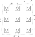
- FIG. 2 is a plan view conceptually showing the backlight film shown in FIG.
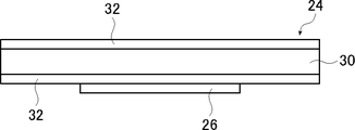
- FIG. 3 is a conceptual diagram for explaining the backlight film shown in FIG.
- FIG. 4 is a diagram conceptually illustrating an example of a planar illumination device that uses another example of the backlight film of the present invention.
- FIG. 1 conceptually shows an example of a planar illumination device 10 that uses an example of a backlight film of the present invention.
- the planar illumination device 10 is a direct-type planar illumination device used in a backlight unit or the like of a liquid crystal display device, and includes a housing 12 having a bottom plate 12a and a light source disposed on the bottom plate 12a of the housing 12. 14 and the backlight film 16 of the present invention.
- the “liquid crystal display device” is also referred to as “LCD”.
- LCD is an abbreviation for “Liquid Crystal Display”.
- FIG. 1 is a schematic diagram only, and the planar illumination device 10 is used for a backlight unit such as an LCD, such as one or more of an LED substrate, wiring, and a heat dissipation mechanism, in addition to the illustrated members.
- a backlight unit such as an LCD
- the planar illumination device 10 is used for an LCD backlight unit or the like. Therefore, in a general usage pattern, in the upper part of the planar illumination device 10 in the figure, various known types of known backlight units such as a light diffusion plate and two prism sheets arranged with ridge lines orthogonal to each other are provided. Further, a liquid crystal panel having a polarizer, a liquid crystal cell, and the like is further disposed thereon.
- the casing 12 is a rectangular casing whose maximum surface is open, and the backlight film 16 of the present invention is disposed so as to close the open surface (see FIG. 4).
- a light source 14 is disposed on the upper surface of the bottom plate 12 a of the housing 12, that is, on the bottom surface of the housing 12.
- the housing 12 is a known housing that is used in a planar illumination device that constitutes a backlight unit of an LCD.
- the bottom surface used as the installation surface of the light source 14 is a light reflection surface selected from a mirror surface, a metal reflective surface, a diffuse reflection surface, etc.
- the housing 12 is preferably a light reflecting surface on the entire inner surface of the housing 12.
- FIG. 2 shows a plan view of the backlight film 16.
- 2 is a view of the backlight film 16 shown in FIG. 1 as viewed from below in FIG.
- the backlight film 16 includes a support 20, a wavelength conversion film 24, and a reflective layer 26.
- the support 20 supports the wavelength conversion film 24. If the support 20 can support the wavelength conversion film 24 and can transmit light emitted from the wavelength conversion film 24 when light is incident from the light source 14 and light emitted from the light source 14 can be transmitted.
- Various sheet-like materials film-like materials, plate-like materials
- the support 20 one or more selected from white polyethylene terephthalate (PET), PET, polyethylene naphthalate (PEN), triacetyl cellulose (TAC), polycarbonate (PC), nylon, and the like. Examples thereof include a resin film made of a resin material and a glass plate.
- the thickness of the support 20 is flat depending on the size of the planar lighting device 10, the material for forming the support 20, the optical function layer (diffuse layer, anti-Newton ring layer, etc.) provided as necessary, and the like. What is necessary is just to set suitably the thickness which can maintain and can support the wavelength conversion film 24 and the reflection layer 26.
- FIG. 1 The thickness of the support 20 is flat depending on the size of the planar lighting device 10, the material for forming the support 20, the optical function layer (diffuse layer, anti-Newton ring layer, etc.) provided as necessary, and the like. What is necessary is just to set suitably the thickness which can maintain and can support the wavelength conversion film 24 and the reflection layer 26.
- the backlight film 16 in the illustrated example has a support 20 that supports the wavelength conversion film 24, and is spaced apart in the surface direction of the support 20, so that the plurality of wavelength conversion films 24 are one main surface of the support 20. Is provided. Each wavelength conversion film 24 is provided with a reflective layer 26. In the illustrated example, one reflection layer 26 is provided on one wavelength conversion film 24. In the present invention, unless otherwise specified, “surface direction” indicates the surface direction of the support 20. Moreover, in this invention, a main surface shows the maximum surface of a sheet-like thing (film, plate-like thing). At this time, the sheet-like material includes a laminate. Further, in the planar illumination device 10, one light source 14 is provided for one wavelength conversion film 24.
- the backlight film 16 of the illustrated example is not preferred to be a wavelength conversion film on the entire surface, but as a preferred embodiment, the wavelength conversion film 24 is arranged two-dimensionally on the support 20 with a small wavelength conversion film 24 spaced apart.
- the amount of the conversion film 24 (quantum dot film (QD (Quantum Dot) film) is reduced and the cost is reduced, which will be described in detail later.
- the wavelength conversion film 24 is two-dimensionally arranged in a square lattice pattern on one main surface of the support 20.
- the arrangement of the wavelength conversion films 24 supported by the support 20 is not limited to the square lattice shape in the illustrated example.
- the wavelength conversion films 24 may be two-dimensionally arranged in any of a staggered lattice shape, an oblique lattice shape, and a hexagonal lattice shape.
- it is preferable that the wavelength conversion films 24 are regularly arranged at regular intervals in that the brightness of light emitted from the backlight film 16 is easily uniformed over the entire surface.
- the support method of the wavelength conversion film 24 by the support body 20 is not limited, and various support methods for known sheet-like materials can be used.
- the wavelength conversion film 24 may be attached to the support 20 by attaching means such as an optical transparent adhesive (OCA (Optical Clear Adhesive)), an optical transparent tape, or an optical transparent double-sided tape.
- OCA optical Clear Adhesive
- the wavelength conversion film 24 may be held on the support 20 using a transparent jig or the like.
- the wavelength conversion film 24 is a known wavelength conversion film that receives light emitted from the light source 14, converts the wavelength, and outputs the converted light.
- FIG. 3 conceptually shows the configuration of the wavelength conversion film 24. 3 is a view of the wavelength conversion film 24 as seen from the same direction as FIG. As shown in FIG. 3, the wavelength conversion film 24 includes a wavelength conversion layer 30 and a gas barrier film 32 that sandwiches and supports the wavelength conversion layer 30.
- the wavelength conversion layer 30 is a fluorescent layer in which a large number of phosphors are dispersed in a matrix such as a resin, and has a function of converting the wavelength of light incident on the wavelength conversion layer 30 and emitting it. is there.
- the wavelength conversion layer 30 converts the wavelength of at least a part of the blue light into red light or green light due to the effect of the phosphor contained therein. Then exit.
- blue light is light having a central wavelength in a wavelength band of 400 to 500 nm
- green light is light having a central wavelength in a wavelength band exceeding 500 nm and not more than 600 nm. Is light having a central wavelength in a wavelength band of more than 600 nm and not more than 680 nm.
- the wavelength conversion function expressed by the fluorescent layer is not limited to the configuration that converts the wavelength of blue light into red light or green light, as long as it converts at least part of incident light into light of a different wavelength. Good.
- the phosphor is excited at least by incident excitation light and emits fluorescence.
- the type of phosphor contained in the phosphor layer there is no limitation on the type of phosphor contained in the phosphor layer, and various known phosphors may be appropriately selected according to the required wavelength conversion performance. Examples of such phosphors include phosphors, aluminates, phosphors doped with rare earth ions in phosphors, aluminates, metal oxides, metal sulfides, metal nitrides, etc. Illustrative examples include a phosphor in which a semiconductor substance is doped with activating ions, a phosphor utilizing a quantum confinement effect known as a quantum dot, and the like.
- a quantum dot having a narrow emission spectrum width capable of realizing a light source excellent in color reproducibility when used in a display, and excellent in light emission quantum efficiency is preferably used in the present invention. That is, in the present invention, as the wavelength conversion layer 30, a quantum dot layer formed by dispersing quantum dots in a matrix such as a resin is preferably used. In the wavelength conversion film 24, as a preferred embodiment, the wavelength conversion layer 30 is a quantum dot layer.
- JP 2012-169271 A for example, paragraphs [0060] to [0066] of JP 2012-169271 A can be referred to, but are not limited to those described here.
- the quantum dots commercially available products can be used without any limitation.
- the emission wavelength of the quantum dots can usually be adjusted by the composition and size of the particles.
- the quantum dots are preferably dispersed uniformly in the matrix, but may be dispersed with a bias in the matrix. Moreover, only 1 type may be used for a quantum dot and it may use 2 or more types together. When using 2 or more types of quantum dots together, you may use 2 or more types of quantum dots from which the wavelength of emitted light differs.
- the known quantum dots include a quantum dot (A) having an emission center wavelength in the wavelength band exceeding 600 nm and in the range of 680 nm, and a quantum dot having an emission center wavelength in the wavelength band exceeding 500 nm and 600 nm.
- (B) There is a quantum dot (C) having an emission center wavelength in a wavelength band of 400 to 500 nm.
- the quantum dots (A) are excited by excitation light to emit red light, the quantum dots (B) emit green light, and the quantum dots (C) emit blue light.
- red light emitted from the quantum dots (A) and light emitted from the quantum dots (B) are emitted.
- White light can be embodied by green light and blue light transmitted through the quantum dot layer.
- red light emitted from the quantum dots (A), quantum dots (B) can be realized by green light emitted by the blue light and blue light emitted by the quantum dots (C).
- quantum dot a so-called quantum rod, a tetrapod type quantum dot, or the like that has a rod shape and has directivity and emits polarized light may be used.
- the wavelength conversion layer 30 is formed by dispersing quantum dots or the like using a resin or the like as a matrix.
- various known matrices used for the quantum dot layer can be used as the matrix, but a matrix obtained by curing a polymerizable composition (coating composition) containing at least two or more polymerizable compounds is preferable.
- the polymerizable group of the polymerizable compound used in combination of at least two may be the same or different.
- the at least two compounds have at least one common polymerizable group. It is preferable.
- the type of the polymerizable group is not particularly limited, but is preferably a (meth) acrylate group, a vinyl group or an epoxy group, or an oxetanyl group, more preferably a (meth) acrylate group, and still more preferably an acrylate group. It is.
- the polymerizable compound that becomes the matrix of the wavelength conversion layer 30 is at least one of the first polymerizable compound made of a monofunctional polymerizable compound and at least one of the second polymerizable compound made of a polyfunctional polymerizable compound.
- the first polymerizable compound and second polymerizable compound can be employed.
- the first polymerizable compound is a monofunctional (meth) acrylate monomer and a monomer having one functional group selected from the group consisting of an epoxy group and an oxetanyl group.
- Monofunctional (meth) acrylate monomers include acrylic acid and methacrylic acid, derivatives thereof, more specifically, (meth) acrylic acid polymerizable unsaturated bond (meth) acryloyl group in the molecule, alkyl Mention may be made of aliphatic or aromatic monomers whose group has 1 to 30 carbon atoms. Specific examples thereof include the following compounds, but the present invention is not limited thereto.
- Aliphatic monofunctional (meth) acrylate monomers include methyl (meth) acrylate, n-butyl (meth) acrylate, isobutyl (meth) acrylate, 2-ethylhexyl (meth) acrylate, isononyl (meth) acrylate, n-octyl ( Alkyl (meth) acrylates having 1 to 30 carbon atoms in the alkyl group, such as (meth) acrylate, lauryl (meth) acrylate, stearyl (meth) acrylate; An alkoxyalkyl (meth) acrylate having 2 to 30 carbon atoms in the alkoxyalkyl group such as butoxyethyl (meth) acrylate; Aminoalkyl (meth) acrylates in which the total number of carbon atoms of the (monoalkyl or dialkyl) aminoalkyl group is 1-20, such as N, N-dimethylaminoe
- aromatic monofunctional acrylate monomer examples include aralkyl (meth) acrylates having 7 to 20 carbon atoms in the aralkyl group such as benzyl (meth) acrylate.
- aralkyl (meth) acrylates having 7 to 20 carbon atoms in the aralkyl group such as benzyl (meth) acrylate.
- aliphatic or aromatic alkyl (meth) acrylates having an alkyl group with 4 to 30 carbon atoms are preferred, and n-octyl (meth) acrylate, lauryl (meth) acrylate are also preferred.
- Examples of monofunctional epoxy compounds having one epoxy group include, for example, phenyl glycidyl ether, p-tert-butylphenyl glycidyl ether, butyl glycidyl ether, 2-ethylhexyl glycidyl ether, allyl glycidyl ether, 1,2-butylene oxide 1,3-butadiene monooxide, 1,2-epoxydodecane, epichlorohydrin, 1,2-epoxydecane, styrene oxide, cyclohexene oxide, 3-methacryloyloxymethylcyclohexene oxide, 3-acryloyloxymethylcyclohexene oxide, Examples include 3-vinylcyclohexene oxide and 4-vinylcyclohexene oxide.
- the monofunctional oxetane compound having one oxetanyl group one obtained by appropriately replacing the epoxy group of the monofunctional epoxy compound described above with an oxetane group can be used.
- a monofunctional compound can be appropriately selected from the oxetane compounds described in JP-A Nos. 2003-341217 and 2004-91556.
- the first polymerizable compound is preferably contained in an amount of 5 to 99.9 parts by mass with respect to a total mass of 100 parts by mass of the first polymerizable compound and the second polymerizable compound, It is preferable that a part by mass is included. The reason will be described later.
- the second polymerizable compound is a monomer having two or more functional groups selected from the group consisting of a polyfunctional (meth) acrylate monomer and an epoxy group and an oxetanyl group in the molecule.
- the bifunctional (meth) acrylate monomers include neopentyl glycol di (meth) acrylate, 1,6-hexanediol di (meth) acrylate, 1,9- Nonanediol di (meth) acrylate, 1,10-decanediol diacrylate, tripropylene glycol di (meth) acrylate, ethylene glycol di (meth) acrylate, tetraethylene glycol di (meth) acrylate, hydroxypivalate neopentyl glycol di Preferred examples include (meth) acrylate, polyethylene glycol di (meth) acrylate, tricyclodecane dimethanol diacrylate, ethoxylated bisphenol A diacrylate, and the like.
- the (meth) acrylate monomers having three or more functions include epichlorohydrin (ECH) modified glycerol tri (meth) acrylate, ethylene oxide (EO) modified glycerol.
- ECH epichlorohydrin
- EO ethylene oxide
- a (meth) acrylate monomer having a urethane bond in the molecule specifically, an adduct of tolylene diisocyanate (TDI) and hydroxyethyl acrylate, isophorone diisocyanate (IPDI) and hydroxyethyl acrylate
- TDI tolylene diisocyanate
- IPDI isophorone diisocyanate
- HDI hexamethylene diisocyanate
- PETA pentaerythritol triacrylate
- Monomers having two or more functional groups selected from the group consisting of epoxy groups and oxetanyl groups include, for example, aliphatic cyclic epoxy compounds, bisphenol A diglycidyl ether, bisphenol F diglycidyl ether, bisphenol S diglycidyl ether, bromine Bisphenol A diglycidyl ether, brominated bisphenol F diglycidyl ether, brominated bisphenol S diglycidyl ether, hydrogenated bisphenol A diglycidyl ether, hydrogenated bisphenol F diglycidyl ether, hydrogenated bisphenol S diglycidyl ether, 1,4 -Butanediol diglycidyl ether, 1,6-hexanediol diglycidyl ether, glycerin triglycidyl ether, trimethylolpropane triglycidyl ether , Polyethylene glycol diglycidyl ether, polypropylene glycol diglycidyl ethers; polyether
- a monomer having two or more functional groups selected from the group consisting of an epoxy group and an oxetanyl group may be produced by any method.
- Maruzen KK Publishing Co., Ltd., Fourth Edition Experimental Chemistry Course 20 Organic Synthesis II, 213, 1992, Ed.by Alfred Hasfner The chemistry of heterocyclic compounds-Small Ring Heterocycles part3 Oxiranes, John & Wiley and Sons, An Interscience Publication, New York, 1985, Yoshimura, Adhesion, Vol.29, No.12, 32, 1985, Yoshimura, Adhesion, Vol. 30, No. 5, 42, 1986, Yoshimura, Adhesion, Vol. 30, No. 7, 42, 1986, Japanese Patent Laid-Open No. 11-100308, Japanese Patent No. 2906245, Japanese Patent No. 2926262, etc. Can be synthesized.
- the second polymerizable compound is preferably contained in an amount of 0.1 to 95 parts by mass with respect to a total mass of 100 parts by mass of the first polymerizable compound and the second polymerizable compound, and 15 to 80 parts by mass. Parts are preferably included. The reason will be described later.
- the matrix forming the wavelength conversion layer 30, in other words, the polymerizable composition to be the wavelength conversion layer 30 may contain necessary components such as a viscosity modifier and a solvent, if necessary.
- the polymerizable composition that becomes the wavelength conversion layer 30 is, in other words, a polymerizable composition for forming the wavelength conversion layer 30.
- the polymerizable composition may contain a viscosity modifier as necessary.
- the viscosity modifier is preferably a filler having a particle size of 5 to 300 nm.
- the viscosity modifier is preferably a thixotropic agent for imparting thixotropic properties.
- the thixotropic property refers to the property of reducing the viscosity with respect to the increase in the shear rate in the liquid composition. It refers to a material having a function of imparting sex.
- thixotropic agents include fumed silica, alumina, silicon nitride, titanium dioxide, calcium carbonate, zinc oxide, talc, mica, feldspar, kaolinite (kaolin clay), pyrophyllite (waxite clay), and sericite.
- sericite bentonite, smectite vermiculites (montmorillonite, beidellite, nontronite, saponite, etc.), organic bentonite, organic smectite and the like.
- the polymerizable composition for forming the wavelength conversion layer 30 has a viscosity of 3 to 50 mPa ⁇ s when the shear rate is 500 s ⁇ 1 , and preferably 100 mPa ⁇ s or more when the shear rate is 1 s ⁇ 1 .
- a thixotropic agent In order to adjust the viscosity in this way, it is preferable to use a thixotropic agent.
- the reason why the viscosity of the polymerizable composition is preferably 3 to 50 mPa ⁇ s when the shear rate is 500 s ⁇ 1 , and preferably 100 mPa ⁇ s or more when the shear rate is 1 s ⁇ 1 is as follows.
- the wavelength conversion film 24 As an example of a method for producing the wavelength conversion film 24 (wavelength conversion layer 30), two gas barrier films 32, which will be described later, are prepared, and the polymerization property that becomes the wavelength conversion layer 30 on the surface of one gas barrier film 32 is prepared.
- a manufacturing method including a step of forming a wavelength conversion layer 30 by curing the polymerizable composition after applying another gas barrier film 32 on the applied polymerizable composition after applying the composition.
- the barrier film 32 to which the polymerizable composition is applied is the first base material
- another barrier film 32 that is attached to the polymerizable composition applied to the first base material is the second base material. Also called a substrate.
- the coating film is uniformly coated so that no coating stripes are formed when the polymerizable composition is applied to the first substrate, and the coating film thickness is uniform. From the viewpoint of leveling properties, it is preferable that the polymerizable composition has a low viscosity.
- the second base material is pasted onto the polymerizable composition applied to the first base material, the resistance to pressure at the time of pasting is performed in order to uniformly bond the second base material. From this viewpoint, it is preferable that the polymerizable composition has a high viscosity.
- the aforementioned shear rate 500 s ⁇ 1 is a representative value of the shear rate applied to the polymerizable composition applied to the first substrate, and the shear rate 1 s ⁇ 1 is obtained by attaching the second substrate to the polymerizable composition.
- This is a representative value of the shear rate applied to the polymerizable composition immediately before combining.
- the shear rate 1 s ⁇ 1 is merely a representative value.
- the shear rate applied to is approximately 0 s ⁇ 1 , and the shear rate applied to the polymerizable composition in the actual production process is not limited to 1 s ⁇ 1 .
- the shear rate of 500 s ⁇ 1 is merely a representative value, and the shear rate applied to the polymerizable composition in the actual production process is not limited to 500 s ⁇ 1 .
- the viscosity of the polymerizable composition is 3 when the representative shear rate applied to the polymerizable composition is 500 s -1 when the polymerizable composition is applied to the first substrate.
- the polymerizable composition to be the wavelength conversion layer 30 may contain a solvent as necessary.
- the type and amount of the solvent used are not particularly limited.
- one or a mixture of two or more organic solvents can be used as the solvent.
- the polymerizable composition that becomes the wavelength conversion layer 30 includes trifluoroethyl (meth) acrylate, pentafluoroethyl (meth) acrylate, (perfluorobutyl) ethyl (meth) acrylate, and perfluorobutyl-hydroxypropyl (meth).
- Including compounds having fluorine atoms such as acrylate, (perfluorohexyl) ethyl (meth) acrylate, octafluoropentyl (meth) acrylate, perfluorooctylethyl (meth) acrylate, and tetrafluoropropyl (meth) acrylate Also good. By including these compounds, the coating property can be improved.
- the polymerizable composition to be the wavelength conversion layer 30 may contain a hindered amine compound as necessary.
- the hindered amine compound include 2,2,6,6-tetramethyl-4-piperidylbenzoate, N- (2,2,6,6-tetramethyl-4-piperidyl) dodecylsuccinimide, 1-[( 3,5-ditert-butyl-4-hydroxyphenyl) propionyloxyethyl] -2,2,6,6-tetramethyl-4-piperidyl- (3,5-ditert-butyl-4-hydroxyphenyl) propionate Bis (2,2,6,6-tetramethyl-4-piperidyl) sebacate, bis (1,2,2,6,6-pentamethyl-4-piperidyl) sebacate, bis (1,2,2,6, 6-pentamethyl-4-piperidyl) -2-butyl-2- (3,5-ditert-butyl-4-hydroxybenzyl) malonate,
- the amount of the resin serving as a matrix may be appropriately determined according to the type of functional material included in the wavelength conversion layer 30.
- the resin serving as a matrix is preferably 90 to 99.9 parts by mass, and 92 to 99 parts by mass with respect to 100 parts by mass of the total amount of the quantum dot layer. Is more preferable.
- the thickness of the wavelength conversion layer 30 is preferably 5 to 200 ⁇ m and more preferably 10 to 150 ⁇ m from the viewpoint of handleability and light emission characteristics.
- the thickness of the wavelength conversion layer 30 is intended to be an average thickness. The average thickness is obtained by measuring the thickness of any 10 or more points of the wavelength conversion layer 30 and arithmetically averaging them.
- a polymerization initiator such as a silane coupling agent, etc.
- a silane coupling agent such as a silane coupling agent
- the wavelength conversion film 24 has a configuration in which such a wavelength conversion layer 30 is sandwiched between two gas barrier films 32.
- gas barrier film 32 is also referred to as “barrier film 32”.
- the barrier film 32 is a known gas barrier film formed by forming a gas barrier layer that does not allow oxygen or the like to pass through on the surface of the support substrate.
- the wavelength conversion layer 30 is sandwiched between the two barrier films 32, thereby preventing oxygen and moisture from entering from the main surface of the wavelength conversion layer 30, and the wavelength conversion layer by oxygen and moisture. 30 deterioration is prevented.
- the barrier film 32 preferably has an oxygen permeability of 1 ⁇ 10 ⁇ 2 cc / (m 2 ⁇ day ⁇ atm) or less.
- the barrier film 32 preferably has a water vapor permeability of 1 ⁇ 10 ⁇ 3 g / (m 2 ⁇ day) or less.
- the oxygen permeability may be measured under the conditions of a temperature of 25 ° C.
- the water vapor permeability was measured by the Mocon method under the conditions of a temperature of 40 ° C. and a relative humidity of 90% RH. Further, when the water vapor permeability exceeds the measurement limit of the Mocon method, it may be measured by the calcium corrosion method (the method described in JP-A-2005-283561) under the same conditions.
- the thickness of the barrier film 32 is preferably 5 to 100 ⁇ m, more preferably 10 to 70 ⁇ m, and further preferably 15 to 55 ⁇ m. Setting the thickness of the barrier film 32 to 5 ⁇ m or more is preferable in that the thickness of the wavelength conversion layer 30 can be made uniform when the wavelength conversion layer 30 is formed between the two barrier films 32. Moreover, it is preferable at the point that the thickness of the whole wavelength conversion film 24 containing the wavelength conversion layer 30 can be made thin by making the thickness of the barrier film 32 into 100 micrometers or less.
- the barrier film 32 is preferably transparent. Further, the barrier film 32 may be a rigid sheet shape or a flexible film shape. Furthermore, the barrier film 32 may be a long shape that can be wound, or may be a single-wafer shape that has been cut into predetermined dimensions in advance.
- barrier film 32 various known gas barrier films formed by forming a gas barrier layer exhibiting gas barrier properties on a support substrate can be used.
- a suitable barrier film 32 on the surface of the support substrate, one or more combinations of an inorganic layer as a gas barrier layer and an organic layer serving as a base (formation surface) of the inorganic layer are formed.
- An organic / inorganic laminated gas barrier film is preferably used.
- an organic / inorganic laminate having an organic layer on one surface of a support substrate, an organic layer on the surface of the organic layer, an inorganic layer as a base layer, and a combination of an inorganic layer and a base organic layer Examples of the type of gas barrier film.
- an organic layer is provided on one surface of the supporting substrate, an organic layer is provided on the surface of the organic layer as an underlayer, and a second organic layer is provided on the inorganic layer.
- An organic-inorganic laminated type gas barrier film having two combinations of an inorganic layer and a base organic layer having a second organic layer as a base layer and a second inorganic layer is exemplified.
- an organic-inorganic laminated gas barrier film having three or more combinations of an inorganic layer and a base organic layer can also be used. Basically, the greater the number of combinations of the inorganic layer and the underlying organic layer, the thicker the gas barrier film, but higher gas barrier properties can be obtained.
- “organic / inorganic laminated gas barrier film” is also referred to as “laminated barrier film”.
- the laminated barrier film it is an inorganic layer that mainly exhibits gas barrier properties.
- the uppermost layer that is, the outermost layer on the opposite side of the support substrate, is the inorganic layer, and the inorganic layer is the inner side, regardless of the layer configuration.
- the wavelength conversion layer 30 side is preferable. That is, when using a laminated barrier film as the barrier film 32 of the wavelength conversion film 24, it is preferable to sandwich the wavelength conversion layer 30 with the barrier film 32 with the inorganic layer in contact with the wavelength conversion layer 30. Thereby, it can prevent more suitably that oxygen etc. penetrate
- various known gas barrier films used as the support substrate can be used.
- films made of various plastics are preferably used in that they are easy to make thinner and lighter and are suitable for flexibility.
- polyethylene polyethylene
- PEN polyethylene naphthalate
- PA polyethylene terephthalate
- PVC polyvinyl chloride
- PVA polyvinyl alcohol
- PAN polyacrylonitrile
- PI polyimide
- transparent polyimide polymethyl methacrylate resin
- PMMA polycarbonate
- PC polyacrylate
- PP polypropylene
- PS polystyrene
- PS acrylonitrile-butadiene-styrene copolymer
- ABS cycloolefin
- the resin film which consists of a copolymer (COC), a cycloolefin polymer (COP), and a triacetyl cellulose (TAC) is illustrated suitably.
- the thickness of a support substrate is preferably about 10 to 100 ⁇ m.
- the support substrate may be provided with functions such as antireflection, phase difference control, and light extraction efficiency improvement on the surface of such a plastic film.
- the gas barrier layer mainly includes an inorganic layer that exhibits gas barrier properties and an organic layer that serves as a base layer for the inorganic layer.
- the uppermost layer is an inorganic layer and the inorganic layer side is directed to the wavelength conversion layer 30 as described above.
- the laminated barrier film may have an organic layer for protecting the inorganic layer as the uppermost layer, if necessary.
- a lamination type barrier film may have an organic layer for ensuring adhesiveness with wavelength conversion layer 30 in the uppermost layer as needed.
- the organic layer for ensuring the adhesion may also act as a protective layer for the inorganic layer.
- the organic layer is a base layer of an inorganic layer that mainly exhibits gas barrier properties in the laminated barrier film.
- Various organic layers that are used as organic layers in known laminated barrier films can be used.
- the organic layer is a film containing an organic compound as a main component, and basically formed by crosslinking monomers and / or oligomers.
- the multilayer barrier film has an organic layer as a base for the inorganic layer, thereby embedding irregularities on the surface of the support substrate and foreign matters adhering to the surface, thereby making the film-forming surface of the inorganic layer appropriate. .
- an appropriate inorganic layer can be formed on the entire surface of the film formation without gaps and without cracks or cracks.
- the oxygen permeability is 1 ⁇ 10 ⁇ 2 cc / (m 2 ⁇ day ⁇ atm) or less and the water vapor permeability is 1 ⁇ 10 ⁇ 3 g / (m 2 ⁇ day) or less.
- Gas barrier performance can be obtained.
- the laminated barrier film since the laminated barrier film has an organic layer serving as the base, the organic layer also functions as a cushion for the inorganic layer. Therefore, when the inorganic layer receives an impact from the outside, damage to the inorganic layer can be prevented by the cushion effect of the organic layer. Thereby, in a laminated type barrier film, an inorganic layer expresses gas barrier performance appropriately, and it can prevent suitably degradation of wavelength conversion layer 30 by moisture and oxygen.
- various organic compounds can be used as the material for forming the organic layer.
- polyester acrylic resin, methacrylic resin, methacrylic acid-maleic acid copolymer, polystyrene, transparent fluororesin, polyimide, fluorinated polyimide, polyamide, polyamideimide, polyetherimide, cellulose acylate, polyurethane, poly Ether ether ketone, polycarbonate, alicyclic polyolefin, polyarylate, polyether sulfone, polysulfone, fluorene ring modified polycarbonate, alicyclic modified polycarbonate, fluorene ring modified polyester, and thermoplastic resin such as acryloyl compound, or polysiloxane,
- Other organic silicon compound films are preferably exemplified. A plurality of these may be used in combination.
- an organic layer composed of a polymer of a radical polymerizable compound and / or a cationic polymerizable compound having an ether group as a functional group is preferable in terms of excellent glass transition temperature and strength.
- the glass transition temperature is 120 ° C. mainly composed of acrylate and / or methacrylate monomers or oligomer polymers in terms of low refractive index, high transparency and excellent optical properties.
- the above acrylic resin and methacrylic resin are preferably exemplified as the organic layer.
- bifunctional or more especially 3 such as dipropylene glycol di (meth) acrylate (DPGDA), trimethylolpropane tri (meth) acrylate (TMPTA), and dipentaerythritol hexa (meth) acrylate (DPHA).
- DPGDA dipropylene glycol di (meth) acrylate
- TMPTA trimethylolpropane tri (meth) acrylate
- DPHA dipentaerythritol hexa
- acrylic resins and methacrylic resins which are mainly composed of a functional or higher acrylate and / or methacrylate monomer or oligomer polymer. It is also preferable to use a plurality of these acrylic resins and methacrylic resins.
- the inorganic layer By forming the organic layer with such an acrylic resin, a methacrylic resin, or the like, the inorganic layer can be formed on a base having a solid skeleton, so that a denser inorganic layer having a high gas barrier property can be formed.
- the thickness of the organic layer is preferably 1 to 5 ⁇ m.
- the thickness of the organic layer is more preferably 1 to 3 ⁇ m.
- the thickness of each organic layer may be the same or different from each other.
- the material for forming each organic layer may be the same or different. However, in terms of productivity and the like, it is preferable to form all organic layers with the same material.
- the organic layer may be formed by a known method such as a coating method or flash vapor deposition. Moreover, in order to improve adhesiveness with the inorganic layer used as the lower layer of an organic layer, it is preferable that an organic layer contains a silane coupling agent.
- An inorganic layer is a film
- membrane which has an inorganic compound as a main component, and mainly expresses the gas barrier property in a lamination type barrier film.
- metal oxides such as aluminum oxide, magnesium oxide, tantalum oxide, zirconium oxide, titanium oxide, and indium tin oxide (ITO); metal nitrides such as aluminum nitride; metal carbides such as aluminum carbide; silicon oxide, Silicon oxides such as silicon oxynitride, silicon oxycarbide and silicon oxynitride carbide; silicon nitrides such as silicon nitride and silicon nitride carbide; silicon carbides such as silicon carbide; hydrides thereof; mixtures of two or more of these; and Films made of inorganic compounds such as these hydrogen-containing materials are preferably exemplified.
- silicon is also regarded as a metal.
- a film made of a silicon compound such as silicon oxide, silicon nitride, silicon oxynitride and silicon oxide is preferably exemplified in that it has high transparency and can exhibit excellent gas barrier properties.
- a film made of silicon nitride is preferable because it has high transparency in addition to more excellent gas barrier properties.
- the materials for forming the inorganic layers may be different from each other. However, in terms of productivity and the like, it is preferable to form all inorganic layers with the same material.
- the thickness of the inorganic layer is preferably 10 to 200 nm.
- the inorganic layer is generally brittle, and if it is too thick, there is a possibility that cracking, cracking, peeling, etc. may occur.
- the thickness of the inorganic layer 200 nm or less it is possible to prevent the occurrence of cracking. .
- the thickness of the inorganic layer is preferably 10 to 100 nm, and more preferably 15 to 75 nm.
- the thickness of each inorganic layer may be the same or different.
- the inorganic layer may be formed by a known method depending on the forming material. Specifically, vapor phase deposition methods such as CCP (Capacitively Coupled Plasma) -CVD (chemical vapor deposition) and ICP (Inductively Coupled Plasma) -CVD, etc., sputtering such as magnetron sputtering and reactive sputtering, and vacuum deposition. Is preferably exemplified.
- the area (size in the surface direction) of the wavelength conversion film 24 formed by sandwiching the wavelength conversion layer 30 with such a barrier film 32 is not limited, and is appropriately determined according to the size of the planar lighting device 10 and the like. , You can set. Specifically, as shown in the illustrated example, in the backlight film 16 having a plurality of wavelength conversion films 24 that are separated in the surface direction of the support 20, the wavelength conversion film 24 has an area of 1000 mm 2 or less. Is preferred. By setting the area of the wavelength conversion film 24 to 1000 mm 2 or less, it is preferable in that the effect of reducing the amount of use of the wavelength conversion film 24 by using a plurality of small wavelength conversion films 24 apart from each other can be suitably obtained.
- the total area of the plurality of wavelength conversion films 24 with respect to the area of the support 20 is not limited, and the number of light sources 14, the area of the support 20, and the luminance of light required for the backlight film 16. It may be set as appropriate according to the above. According to the study by the present inventors, the total area of the wavelength conversion film 24 relative to the area of the support 20 is preferably 20% or less, which is preferable in that the amount of the wavelength conversion film 24 used can be sufficiently reduced.
- the thickness of the wavelength conversion film 24 is not limited, and may be set as appropriate according to the material for forming the wavelength conversion layer 30, the material for forming the barrier film 32, and the layer configuration. That is, the preferred thickness of the wavelength conversion film 24 is basically a thickness corresponding to the preferred thickness of the wavelength conversion layer 30 and the preferred thickness of the barrier film 32 described above.
- the wavelength conversion film 24 may have a light diffusion layer on the surface of the barrier film 32 opposite to the support 20. That is, when the barrier film 32 is the above-described laminated barrier film, a light diffusion layer may be provided on the surface of the support substrate opposite to the support 20.
- the wavelength conversion film 24 having the light diffusion layer leads to an increase in the amount of excitation light incident on the wavelength conversion layer 30, the amount of light emitted from the wavelength conversion layer 30, etc.
- the brightness of an LCD or the like that uses the planar illumination device 10 can be improved.
- a light diffusion layer formed by dispersing a light diffusing agent in a binder such as a resin
- a binder various types of resins, such as various resins, which are used in a light diffusion layer formed by dispersing a light diffusion agent in a binder can be used.
- the light diffusing agent various types such as various inorganic particles used for a light diffusing layer in which a light diffusing agent is dispersed in a binder can be used.
- the reflection layer 26 may be formed on the light diffusion layer, or the light diffusion layer is not formed at the position where the reflection layer 26 is provided.
- the reflective layer 26 may be directly formed on the barrier film 32 (support substrate). However, it is preferable that the wavelength conversion film 24 does not have a light diffusion layer at a position where the reflective layer 26 is formed, in that the thickness of the reflective layer 26 can be made uniform. That is, in the case of the laminated barrier film described above, the reflective layer 26 is preferably provided directly on the support substrate of the barrier film 32.
- the wavelength conversion film 24 preferably covers the end surface with an end surface sealing layer made of a material that exhibits gas barrier properties. Thereby, oxygen or the like can also be prevented from entering the wavelength conversion layer 30 from the end face of the wavelength conversion film 24.
- an end face sealing layer a metal layer such as a plating layer, an inorganic compound layer such as a silicon oxide layer and / or a silicon nitride layer, a resin layer made of a resin material such as an epoxy resin or a polyvinyl alcohol resin, or the like, such as oxygen or moisture
- a metal layer such as a plating layer, an inorganic compound layer such as a silicon oxide layer and / or a silicon nitride layer, a resin layer made of a resin material such as an epoxy resin or a polyvinyl alcohol resin, or the like, such as oxygen or moisture
- a resin material such as an epoxy resin or a polyvinyl alcohol resin, or the like
- the end face sealing layer has a multi-layer configuration such as a configuration including a base metal layer and a plating layer, and a configuration including a lower layer (wavelength conversion film 24 side) polyvinyl alcohol layer and an upper epoxy resin layer. Also good.
- a reflective layer 26 is provided on the surface of the wavelength conversion film 24 opposite to the support 20, that is, on the light incident surface from the light source 14.
- the reflective layer 26 is a circular sheet (a plate or a film).
- the reflective layer 26 and the wavelength conversion film 24 are arranged so that the center of the circle and the center of the square coincide with each other.
- one light source 14 is provided for one wavelength conversion film 24.
- the light source 14 is arranged in the plane direction so that the optical axis coincides with the center of the circular reflective layer 26.
- the backlight film 16 in the illustrated example has a support 20 as a preferred embodiment, and has a configuration in which a large number of small wavelength conversion films 24 are provided on one main surface of the support 20 in a state of being separated from each other.
- the backlight film 16 has a configuration in which the wavelength conversion films 24 are arranged in a square lattice pattern.
- the wavelength conversion film 24 and the light source 14 are arranged close to each other, the luminance of light incident on the wavelength conversion film is increased. Moreover, if high-intensity light enters, the temperature rise of the wavelength conversion film by the incident light will also become large.
- the wavelength conversion film 24 in the illustrated example uses a blue LED as the light source 14 because the wavelength conversion layer 30 is a quantum dot layer using quantum dots.
- blue light has a high energy due to its short wavelength.
- the resin or the like constituting the wavelength conversion layer 30 is likely to deteriorate. Therefore, if the light source 14 and the wavelength conversion film 24 are arranged close to each other, the wavelength conversion layer 30 deteriorates with time and cannot emit predetermined light, that is, the durability of the wavelength conversion film becomes insufficient. Problem arises.
- the planar illumination device 10 using the backlight film 16 of the present invention is used for an LCD backlight unit or the like. Therefore, on the light emitting surface of the planar illumination device 10, a diffusion plate, two prism sheets arranged with the ridge lines orthogonal to each other are arranged in order to make the light uniform in the surface direction of the LCD. . Therefore, as shown in FIGS. 1 and 2, even if the wavelength conversion film 24 is spaced apart and two-dimensionally arranged, the light incident on the liquid crystal display panel of the LCD can be made substantially uniform in the plane direction.
- the backlight film 16 emits light and enters the liquid crystal display panel of the LCD. Will occur. That is, when the area of the reflective layer 26 is different, the amount of light that is transmitted through the reflective layer 26 and incident on the wavelength conversion film 24 (wavelength conversion layer 30) varies depending on the area of the reflective layer 26. If the amount of light that is transmitted through the reflective layer 26 and is incident on the wavelength conversion layer 30 is different, the amount of light that is incident on the wavelength conversion layer 30 is also different, so that the color of the light emitted from the wavelength conversion layer 30 is also different.
- the color of light emitted from the wavelength conversion film 24 varies for each region where the reflective layer 26 is formed in accordance with the area variation of the reflective layer 26.
- the color of the light emitted from each wavelength conversion film 24 varies according to the area variation of the reflective layer 26.
- the color of the emitted light differs for each wavelength conversion film 24, resulting in color unevenness. That is, color unevenness occurs in which the color of the emitted light is different for each wavelength conversion film 24.
- the wavelength conversion film 24 has a reflection layer 26 for preventing the wavelength conversion layer 30 from being deteriorated due to light or heat, and the reflection layer 26 has an area variation. Is ⁇ 5% or less. Therefore, the backlight film 16 of the present invention can make the color of the light emitted from each wavelength conversion film 24 uniform. As a result, by using the backlight film 16 of the present invention, backlight light having no color unevenness in the surface direction can be incident on the liquid crystal panel, and the LCD can display a high-quality image without color unevenness.
- the area variation of the reflective layer 26 exceeds ⁇ 5%, due to the area variation of the reflective layer 26, the color unevenness, that is, the color difference of the light emitted from each wavelength conversion film 24 becomes large.
- color unevenness luminance unevenness
- the area variation of the reflective layer 26 is preferably ⁇ 3% or less in that the color unevenness of the light emitted from the wavelength conversion film 24 can be reduced.
- the area variation (area variation) of the reflective layer 26 is ⁇ 5% or less.
- the area of all the reflective layers 26 is relative to the average area of the reflective layer 26 provided on the backlight film 16. It shows that it is ⁇ 5% or less of the average area.
- the area of the reflective layer 26 is an area in the surface direction. In other words, the area of the reflective layer 26 is the area of the reflective layer 26 at the interface between the reflective layer 26 and the wavelength conversion film 24.
- the reflectance of light by the reflective layer 26 is not particularly limited, and a reflectance that can sufficiently prevent the wavelength conversion layer 30 from being deteriorated by light irradiated by the light source 14 may be set as appropriate.
- the light source 14 is preferably a blue LED that emits blue light.
- the reflective layer 26 preferably reflects 50 to 90%, more preferably 70 to 80%, of light (blue light) in the wavelength range of 420 to 490 nm. That is, the reflective layer 26 preferably has a blue light transmittance of 10 to 50%. By making the reflectance of the blue light by the reflective layer 26 be 50% or more, it is preferable in that the deterioration of the wavelength conversion layer 30 can be suitably prevented.
- the reflectance of blue light by the reflective layer 26 is preferable in that sufficient light (excitation light) can be incident on the wavelength conversion layer 30.
- the higher the blue light reflectance by the reflective layer 26, the greater the difference in the amount of light incident on the wavelength conversion layer 30 due to the difference in the area of the reflective layer 26, and the light emitted from the wavelength conversion film 24.
- Brightness difference that is, color unevenness for each wavelength conversion film 24 increases.
- the reflectance of the blue light by the reflective layer 26 is 80% or less, the color unevenness of the emitted light of the wavelength conversion film 24 due to the area variation of the reflective layer 26 can be suppressed.
- the area of the reflective layer 26 is preferably 1 to 30%, more preferably 5 to 10% with respect to the area of the wavelength conversion film 24. .
- the area of the reflective layer 26 1% or more with respect to the area of the wavelength conversion film 24, it is preferable in that the deterioration of the wavelength conversion layer 30 due to light or heat can be suitably prevented.
- the area of the reflective layer 26 30% or less with respect to the area of the wavelength conversion film 24, it is preferable in that sufficient light can be incident on the wavelength conversion layer 30.
- the shape of the reflective layer 26 is not limited to the circular shape in the illustrated example, and various shapes such as a square, a rectangle, an ellipse, and a triangle can be used.
- the reflection layer 26 is also circular, and the optical axis of the light source 14 and the circle of the reflection layer 26 are circular. It is preferable to match the center.
- the reflective layer 26 has an elliptical shape or a rectangular shape, light from a plurality of light sources may be incident on one reflective layer 26.
- reflection layers 26 having different shapes such as a circular reflection layer 26 and a square reflection layer 26 may be mixed. That is, in the present invention, it is important that the area of light that is transmitted through the reflective layer 26 and incident on the wavelength conversion film 24 (wavelength conversion layer 30) is uniform, and if the area variation is ⁇ 5% or less.
- Various shapes of reflective layers may be mixed.
- one reflective layer is provided on one small wavelength conversion film, but the present invention is not limited to this.
- two reflection layers 26 may be provided on one wavelength conversion film, and light from two light sources may be incident on one wavelength conversion film.
- one reflection layer 26 is formed on one wavelength conversion film 24. It is considered that it is advantageous to provide one light source 14 in terms of reducing the amount of wavelength conversion film used.
- the reflective layer 26 is not limited, and various known optical materials used as the reflective layer in various known optical devices and optical elements can be used. Therefore, the reflection layer 26 may be a reflection layer by diffuse reflection such as a diffusion plate, a reflection layer by interference reflection such as a laminated film, or a reflection layer by mirror reflection such as a metal film. These reflective layers 26 may be formed by a known method.
- the reflection layer 26 is preferably a reflection layer by diffuse reflection in which diffusion particles are dispersed in a binder serving as a matrix.
- the binder used as the matrix is preferably exemplified by a resin (polymer compound) obtained by polymerizing a polymerizable compound.
- Preferred polymerizable compounds include, for example, compounds having an ethylenically unsaturated bond in at least one of the terminal and side chains and / or compounds having an epoxy group or oxetane group in at least one of the terminal and side chains.
- a compound having an ethylenically unsaturated bond at least one of a terminal and a side chain is more preferable.
- the compound having an ethylenically unsaturated bond at at least one of the terminal and the side chain include (meth) acrylate compounds, acrylamide compounds, styrene compounds, maleic anhydride, etc., and (meth) acrylate compounds. Compounds are preferred, and acrylate compounds are more preferred.
- As the (meth) acrylate compound (meth) acrylate, urethane (meth) acrylate, polyester (meth) acrylate, epoxy (meth) acrylate and the like are preferable.
- styrene compound styrene, ⁇ -methylstyrene, 4-methylstyrene, divinylbenzene, 4-hydroxystyrene, 4-carboxystyrene and the like are preferable. It is also preferable to use a compound having a fluorene skeleton as the acrylate compound. Specific examples of such compounds include compounds represented by formula (2) described in WO2013 / 047524A1.
- binders formed using a graft copolymer having 500 g / mol or more As such a graft copolymer, for example, a commercially available product such as an ultraviolet curable urethane acrylic polymer (Acryt 8BR series) manufactured by Taisei Fine Chemical Co., Ltd. may be used.
- the content of the diffusing particles may be appropriately set according to the type of the diffusing particles, the light reflectance required for the reflecting layer 26, and the like.
- Application of the paint for forming the reflective layer 26 may be performed by a known method such as a dispenser method, an inkjet method, or a printing method such as screen printing.
- the backlight film of the present invention can be used not only for a direct type surface illumination device as shown in FIGS. 1 to 4, but also for a so-called edge light type surface illumination device using a light guide plate. Is possible.
- the backlight film of the present invention may be disposed between the light source and the light incident surface of the light guide plate in correspondence with the light source and the reflective layer.
- Trimethylolpropane triacrylate manufactured by Daicel Cytec Co., Ltd.
- a photopolymerization initiator Liberti Co., Ltd., ESACURE KTO46
- a coating solution having a solid content concentration of 15% was obtained. This coating solution was applied to the support substrate by roll-to-roll using a die coater, and allowed to pass through a 50 ° C. drying zone. The residence time in the drying zone was 3 minutes.
- a silicon nitride layer was formed as an inorganic layer on the surface of the organic layer using an RtoR CVD apparatus.
- source gases silane gas (flow rate 160 sccm), ammonia gas (flow rate 370 sccm), hydrogen gas (flow rate 590 sccm), and nitrogen gas (flow rate 240 sccm) were used.
- a power source a high frequency power source having a frequency of 13.56 MHz was used.
- the film formation pressure was 40 Pa and the ultimate film thickness was 50 nm.
- Quantum dot-containing polymerizable composition >> Toluene dispersion of quantum dots 1 (emission maximum: 535 nm) 10 parts by mass Toluene dispersion of quantum dots 2 (emission maximum: 630 nm) 1 part by weight Lauryl methacrylate 40 parts by weight Bifunctional methacrylate 4G (manufactured by Shin-Nakamura Chemical Co., Ltd.) 20 Mass part Trifunctional acrylate TMPTA (Daicel Cytec Co., Ltd.) 20 parts by mass Urethane acrylate UA-160TM (Shin Nakamura Kogyo Co., Ltd.) 10 parts by mass Silane coupling agent KBM-5103 (Shin-Etsu Chemical Co., Ltd.) 10 parts by mass Photopolymerization start Irgacure 819 (manufactured by BASF) 1 part by mass
- ⁇ Preparation of paint for forming reflective layer 26> 0.31 g of polymethyl methacrylate (manufactured by Mitsubishi Rayon Co., Ltd., dialnal BR-88, weight average molecular weight 1.300,000 g / mol) was placed in a solvent of 4.18 g of methyl ethyl ketone and dissolved by stirring for 12 hours.
- the area of the reflective layer 26 of each wavelength conversion film 24 was measured with a microscope (manufactured by Keyence Corporation, VW9000). As a result, the average area of the reflective layer 26 was 232 mm 2 , and the area variation of the reflective layer 26 was ⁇ 4.6%.
- a PET film (A4300, manufactured by Toyobo Co., Ltd.) having a size in the plane direction of 100 ⁇ 100 mm and a thickness of 50 ⁇ m was prepared.
- a wavelength conversion film 24 having a reflective layer 26 formed thereon was attached to the support 20 at an equal interval of 25 mm to produce a backlight film 16.
- the wavelength conversion film 24 was attached to the support 20 with the reflective layer 26 opposite to the support 20.
- the wavelength conversion film 24 was attached by OCA (manufactured by 3M, 8172CL).
- ⁇ Preparation of the planar lighting device 10> As the housing 12, a rectangular housing having one opening surface of 150 ⁇ 150 mm and a mirror surface on the inner surface was prepared. When the opening surface of the housing 12 is closed by a flat plate with a mirror film, the center of the reflective layer 26 coincides with the optical axis so that four light sources 14 are provided. Fixed. As the light source 14, a blue LED (manufactured by Nichia Corporation, NSPB346KS, peak wavelength 450 nm, full width at half maximum 55 nm) was used. Next, the surface of the housing 12 on which the backlight film 16 was pasted was closed with a mirror-like flat plate to produce a planar lighting device 10 as shown in FIG.
- NSPB346KS peak wavelength 450 nm, full width at half maximum 55 nm
- the backlight film 16 was bonded to the flat mirror surface with the support 20 facing the flat film, and the flat plate closed the casing 12 with the mirror surface side as the inner surface side.
- the flat plate is transparent only in the attachment position of the film for backlights.
- the distance between the light source 14 and the wavelength conversion film 24 was such that the diameter of the blue light emitted from the light source 14 on the surface of the wavelength conversion film 24 was 20 mm.
- Example 2 In the formation of the reflective layer 26, a backlight film 16 was produced in the same manner as in Example 1 except that the application pattern with the dispenser was changed. As in Example 1, the area of the reflective layer 26 of each wavelength conversion film 24 was measured. As a result, the average area of the reflective layer 26 was 232 m 2 and the area variation was ⁇ 2.4%. A planar illumination device 10 was produced in the same manner as in Example 1 except that this backlight film 16 was used.
- the luminance distribution and durability of each planar lighting device thus manufactured were measured as follows.
- the wavelength conversion film 24 has the reflective layer 26, and the backlight film of the present invention in which the area variation of the reflective layer 26 is ⁇ 5% or less includes the blue LEDs arranged close to each other. However, it has excellent durability and has little color unevenness of emitted light.
- the backlight film of Comparative Example 1 that does not have the reflective layer 26 it is considered that the wavelength conversion layer 30 was deteriorated by the light and heat of the blue LED adjacent thereto, and the color unevenness of the emitted light is large. Further, the post-durability test luminance L1 is significantly reduced with respect to the initial luminance L0.
- the reflective layer 26 was provided, the backlight film of Comparative Example 2 in which the area variation of the reflective layer 26 exceeded ⁇ 5% produced large color unevenness in the emitted light. From the above results, the effects of the present invention are clear.
- It can be suitably used as an illumination light source for various devices such as LCD backlights.
Landscapes
- Physics & Mathematics (AREA)
- General Physics & Mathematics (AREA)
- Optics & Photonics (AREA)
- Chemical & Material Sciences (AREA)
- Nonlinear Science (AREA)
- Engineering & Computer Science (AREA)
- Mathematical Physics (AREA)
- Crystallography & Structural Chemistry (AREA)
- Manufacturing & Machinery (AREA)
- Materials Engineering (AREA)
- Health & Medical Sciences (AREA)
- Chemical Kinetics & Catalysis (AREA)
- Medicinal Chemistry (AREA)
- Polymers & Plastics (AREA)
- Organic Chemistry (AREA)
- Dispersion Chemistry (AREA)
- General Engineering & Computer Science (AREA)
- Planar Illumination Modules (AREA)
- Liquid Crystal (AREA)
- Optical Filters (AREA)
- Optical Elements Other Than Lenses (AREA)
Abstract
液晶ディスプレイ等に用いられる、波長変換フィルムを利用するバックライト用フィルムであって、耐久性が良好で、バックライトユニットにおいて色ムラの無い光の出射を可能にするバックライト用フィルムの提供を課題とする。波長変換層および波長変換層を挟むガスバリアフィルムを有する波長変換フィルムと、波長変換フィルムの一方の主面に設けられる反射層と、を有し、反射層の面積バラツキが±5%以下であることにより、課題を解決する。
Description
本発明は、液晶表示装置のバックライトユニット等に用いられるバックライト用フィルムに関する。
液晶表示装置は、消費電力が小さく、省スペースの画像表示装置として年々その用途が広がっている。また、近年の液晶表示装置において、液晶表示装置の性能改善としてさらなる省電力化、色再現性向上等が求められている。
液晶表示装置のバックライトの省電力化に伴って、光利用効率を高め、また、色再現性を向上するために、バックライトユニットに、入射光の波長を変換する波長変換フィルムを用いることが知られている。また、波長変換フィルムとしては、量子ドットを用いる波長変換フィルムが知られている。
量子ドットを用いる波長変換フィルムは、一例として、樹脂等からなるマトリックス中に、量子ドットを分散してなる量子ドット層を、樹脂フィルム等の支持体で挟持してなる構成を有する。
量子ドットを用いる波長変換フィルムは、一例として、樹脂等からなるマトリックス中に、量子ドットを分散してなる量子ドット層を、樹脂フィルム等の支持体で挟持してなる構成を有する。
量子ドットとは、三次元全方向において移動方向が制限された電子の状態の結晶のことであり、半導体のナノ粒子が、高いポテンシャル障壁で三次元的に囲まれている場合に、このナノ粒子は量子ドットとなる。量子ドットは種々の量子効果を発現する。例えば、量子ドットは、電子の状態密度(エネルギー準位)が離散化される「量子サイズ効果」を発現する。この量子サイズ効果によれば、量子ドットの大きさを変化させることで、光の吸収波長および/または発光波長を制御できる。
例えば、特許文献1には、直下型のバックライトユニット等に用いられる照明装置(発光装置)として、光源と、複数の光源を共通に覆う光拡散部材と、各光源に対応する領域に配置され、光源からの第1の波長光を第2の波長光に変換する量子ドット等を用いる波長変換フィルム(波長変換部材)とを有する装置が開示されている。
波長変換フィルムを用いるバックライトユニット等では、光源として、LED(Light Emitting Diode)が用いられる場合が多い。例えば、前述の特許文献1には、光源として、青色LEDを用いることが開示されている。
波長変換フィルムを有効に使うためには、光源であるLED等が出射した光を、全て、波長変換フィルムに入射するのが好ましい。
周知のように、LEDが出射する光は、拡散光である。そのため、LEDが出射した光を全て波長変換フィルムに入射させるためには、波長変換フィルムのサイズ、LEDが出射する光の広がり角(発散角)を考慮して、LEDと波長変換フィルムとを、近接して配置する必要が有る。
周知のように、LEDが出射する光は、拡散光である。そのため、LEDが出射した光を全て波長変換フィルムに入射させるためには、波長変換フィルムのサイズ、LEDが出射する光の広がり角(発散角)を考慮して、LEDと波長変換フィルムとを、近接して配置する必要が有る。
LEDと波長変換フィルムとを、近接して配置すれば、波長変換フィルムに入射する光の輝度は高くなる。また、波長変換フィルムに入射する光の輝度が高くなれば、入射した光による波長変換フィルムの温度上昇も大きくなる。
ところが、本発明者らの検討によれば、LEDと波長変換フィルムとを、近接して配置すると、光や熱によって、量子ドット層を構成する樹脂や量子ドットが劣化(光劣化および熱劣化)して、量子ドット層が劣化してしまう。そのため、LEDと波長変換フィルムとを、近接して配置すると、波長変換フィルムの耐久性が不十分になってしまうという問題が生じる。
また、LEDと波長変換フィルムとを近接しない場合でも、LEDの出力、波長変換フィルムに入射する光の輝度、量子ドット層の形成材料によっては、同様の量子ドット層の劣化が生じ、波長変換フィルムの耐久性が不十分になるという問題が生じる。
また、LEDと波長変換フィルムとを近接しない場合でも、LEDの出力、波長変換フィルムに入射する光の輝度、量子ドット層の形成材料によっては、同様の量子ドット層の劣化が生じ、波長変換フィルムの耐久性が不十分になるという問題が生じる。
本発明の目的は、このような従来技術の問題点を解決することにあり、光源からの光および熱による波長変換フィルムの劣化を防止でき、耐久性が高く長寿命で、さらに、バックライトユニットにおいて色ムラの無い光の出射を可能にするバックライト用フィルムを提供することにある。
このような目的を達成するために、本発明のバックライト用フィルムは、波長変換層および波長変換層を挟むガスバリア層を有する波長変換フィルムと、
波長変換フィルムの一方の主面に設けられる複数の反射層と、を有し、
反射層の面積バラツキが±5%以下であることを特徴とするバックライト用フィルムを提供する。
波長変換フィルムの一方の主面に設けられる複数の反射層と、を有し、
反射層の面積バラツキが±5%以下であることを特徴とするバックライト用フィルムを提供する。
このような本発明のバックライト用フィルムにおいて、波長変換フィルムを支持する支持体を有し、複数の波長変換フィルムを支持体面上に有し、波長変換フィルム同士は支持体の面方向に離間して設けられ、かつ、個々の波長変換フィルム毎に反射層が少なくとも1つ設けられるのが好ましい。
また、波長変換フィルムの大きさが1000mm2以下であるのが好ましい。
また、反射層は、420~490nmの波長域の光を50~90%、反射するのが好ましい。
さらに、反射層の面積が、波長変換フィルムの面積に対して0.1~80%であるのが好ましい。
また、波長変換フィルムの大きさが1000mm2以下であるのが好ましい。
また、反射層は、420~490nmの波長域の光を50~90%、反射するのが好ましい。
さらに、反射層の面積が、波長変換フィルムの面積に対して0.1~80%であるのが好ましい。
このような本発明によれば、液晶表示装置のバックライトユニット等に用いられるバックライト用フィルムにおいて、光源からの光および熱に起因する波長変換層の劣化を防止でき、耐久性が高く長寿命で、さらに、液晶表示装置のバックライトユニット等に使用した際に、色ムラが無い光の出射を可能にする、バックライト用フィルムを提供できる。
以下、本発明のバックライト用フィルムについて、添付の図面に示される好適実施例を基に、詳細に説明する。
以下に記載する構成要件の説明は、本発明の代表的な実施態様に基づいてなされることがあるが、本発明は、そのような実施態様に限定されるものではない。
なお、本明細書において、『~』を用いて表される数値範囲は、『~』の前後に記載される数値を下限値および上限値として含む範囲を意味する。
また、本明細書において、『(メタ)アクリレート』とは、アクリレートとメタクリレートとの少なくとも一方、または、いずれかの意味で用いるものとする。『(メタ)アクリロイル』等も同様である。
以下に記載する構成要件の説明は、本発明の代表的な実施態様に基づいてなされることがあるが、本発明は、そのような実施態様に限定されるものではない。
なお、本明細書において、『~』を用いて表される数値範囲は、『~』の前後に記載される数値を下限値および上限値として含む範囲を意味する。
また、本明細書において、『(メタ)アクリレート』とは、アクリレートとメタクリレートとの少なくとも一方、または、いずれかの意味で用いるものとする。『(メタ)アクリロイル』等も同様である。
図1に、本発明のバックライト用フィルムの一例を利用する、面状照明装置10の一例を概念的に示す。
面状照明装置10は、液晶表示装置のバックライトユニット等に用いられる、直下型の面状照明装置であって、底板12aを有する筐体12と、筐体12の底板12aに配置される光源14と、本発明のバックライト用フィルム16とを有する。
以下の説明では、『液晶表示装置』を『LCD』ともいう。『LCD』とは『Liquid Crystal Display』の略である。
面状照明装置10は、液晶表示装置のバックライトユニット等に用いられる、直下型の面状照明装置であって、底板12aを有する筐体12と、筐体12の底板12aに配置される光源14と、本発明のバックライト用フィルム16とを有する。
以下の説明では、『液晶表示装置』を『LCD』ともいう。『LCD』とは『Liquid Crystal Display』の略である。
なお、図1は、あくまで模式図であって、面状照明装置10は、図示した部材以外にも、例えば、LED基板、配線および放熱機構の1以上など、LCD等のバックライトユニットに利用される公知の照明装置に設けられる、公知の各種の部材を有してもよい。
また、面状照明装置10は、LCDのバックライトユニットなどに利用されるものである。そのため、一般的な使用形態では、面状照明装置10の図中上方には、光拡散板、稜線を直交して配置される2枚のプリズムシートなど、公知のバックライトユニットが有する公知の各種の部材が配置され、さらに、その上に、偏光子および液晶セル等を有する液晶パネル等が配置される。
また、面状照明装置10は、LCDのバックライトユニットなどに利用されるものである。そのため、一般的な使用形態では、面状照明装置10の図中上方には、光拡散板、稜線を直交して配置される2枚のプリズムシートなど、公知のバックライトユニットが有する公知の各種の部材が配置され、さらに、その上に、偏光子および液晶セル等を有する液晶パネル等が配置される。
筐体12は、一例として、最大面が開放する矩形の筐体であって、開放面を閉塞するように、本発明のバックライト用フィルム16が配置される(図4参照)。また、筐体12の底板12aの上面すなわち筐体12の底面には、光源14が配置される。
筐体12は、LCDのバックライトユニットを構成する面状照明装置に利用される、公知の筐体である。
また、筐体12は、好ましい態様として、少なくとも光源14の設置面となる底面は、鏡面、金属反射面および拡散反射面等から選択される光反射面となっている。筐体12は、好ましくは、筐体12の内面全面が、光反射面となっている。
筐体12は、LCDのバックライトユニットを構成する面状照明装置に利用される、公知の筐体である。
また、筐体12は、好ましい態様として、少なくとも光源14の設置面となる底面は、鏡面、金属反射面および拡散反射面等から選択される光反射面となっている。筐体12は、好ましくは、筐体12の内面全面が、光反射面となっている。
図2に、バックライト用フィルム16の平面図を示す。なお、図2は、図1に示すバックライト用フィルム16を、図1の下方から見た図である。
バックライト用フィルム16は、支持体20と、波長変換フィルム24と、反射層26とを有して構成される。
バックライト用フィルム16は、支持体20と、波長変換フィルム24と、反射層26とを有して構成される。
支持体20は、波長変換フィルム24を支持するものである。
支持体20は、波長変換フィルム24を支持可能で、かつ、光源14から光を入射されることで波長変換フィルム24が出射する光、および、光源14が出射した光が透過可能であれば、各種のシート状物(フィルム状物、板状物)が利用可能である。
具体的には、支持体20としては、白色ポリエチレンテレフタレート(PET)、PET、ポリエチレンナフタレート(PEN)、トリアセチルセルロース(TAC)、ポリカーボネート(PC)、および、ナイロン等から選択される1以上の樹脂材料からなる樹脂フィルム、ガラス板等が例示される。
支持体20は、波長変換フィルム24を支持可能で、かつ、光源14から光を入射されることで波長変換フィルム24が出射する光、および、光源14が出射した光が透過可能であれば、各種のシート状物(フィルム状物、板状物)が利用可能である。
具体的には、支持体20としては、白色ポリエチレンテレフタレート(PET)、PET、ポリエチレンナフタレート(PEN)、トリアセチルセルロース(TAC)、ポリカーボネート(PC)、および、ナイロン等から選択される1以上の樹脂材料からなる樹脂フィルム、ガラス板等が例示される。
支持体20の厚さは、面状照明装置10のサイズ、支持体20の形成材料、必要に応じて設けられる光学機能層(拡散層およびアンチニュートンリング層など)等に応じて、平面状を保ち、かつ、波長変換フィルム24および反射層26を支持できる厚さを、適宜、設定すればよい。
なお、支持体20は、設計および面状照明装置10の用途等に応じて、任意の形状を利用することができる。
図示例のバックライト用フィルム16は、波長変換フィルム24を支持する支持体20を有し、支持体20の面方向に離間して、複数の波長変換フィルム24が支持体20の一方の主面に設けられる。また、各波長変換フィルム24には、反射層26が設けられる。図示例においては、1枚の波長変換フィルム24に、1個の反射層26が設けられる。
なお、本発明において、特に説明がない場合には、『面方向』とは支持体20の面方向を示す。また、本発明において、主面とは、シート状物(フィルム、板状物)の最大面を示す。この際において、シート状物には積層体も含む。
さらに、面状照明装置10では、1枚の波長変換フィルム24に対して、1個の光源14が設けられる。
図示例のバックライト用フィルム16は、好ましい態様として、全面を波長変換フィルムとするのではなく、支持体20に、小型の波長変換フィルム24を離間して二次元的に配列することにより、波長変換フィルム24(量子ドットフィルム(QD(Quantum Dot)フィルム)の使用量を減らして、かつ、コストダウンも図っている。この点に関しては、後に詳述する。
なお、本発明において、特に説明がない場合には、『面方向』とは支持体20の面方向を示す。また、本発明において、主面とは、シート状物(フィルム、板状物)の最大面を示す。この際において、シート状物には積層体も含む。
さらに、面状照明装置10では、1枚の波長変換フィルム24に対して、1個の光源14が設けられる。
図示例のバックライト用フィルム16は、好ましい態様として、全面を波長変換フィルムとするのではなく、支持体20に、小型の波長変換フィルム24を離間して二次元的に配列することにより、波長変換フィルム24(量子ドットフィルム(QD(Quantum Dot)フィルム)の使用量を減らして、かつ、コストダウンも図っている。この点に関しては、後に詳述する。
図示例のバックライト用フィルム16において、波長変換フィルム24は、支持体20の一方の主面に、正方格子状に二次元的に配列される。
なお、本発明において、支持体20に支持される波長変換フィルム24の配列は、図示例の正方格子状に限定はされない。例えば、波長変換フィルム24を、千鳥格子状、斜方格子状および六角格子状のいずれかで二次元的に配列してもよい。
いずれにしても、バックライト用フィルム16から出射する光の輝度を全面的に均一にし易い等の点で、波長変換フィルム24は、等間隔かつ規則的に配列するのが好ましい。
なお、本発明において、支持体20に支持される波長変換フィルム24の配列は、図示例の正方格子状に限定はされない。例えば、波長変換フィルム24を、千鳥格子状、斜方格子状および六角格子状のいずれかで二次元的に配列してもよい。
いずれにしても、バックライト用フィルム16から出射する光の輝度を全面的に均一にし易い等の点で、波長変換フィルム24は、等間隔かつ規則的に配列するのが好ましい。
なお、支持体20による波長変換フィルム24の支持方法は、限定はなく、公知のシート状物の支持方法が、各種、利用可能である。
一例として、光学透明接着剤(OCA(Optical Clear Adhesive))、光学透明テープおよび光学透明両面テープのいずれかなどの貼着手段によって、波長変換フィルム24を支持体20に貼着すればよい。あるいは、透明な治具等を用いて、波長変換フィルム24を支持体20に保持してもよい。
一例として、光学透明接着剤(OCA(Optical Clear Adhesive))、光学透明テープおよび光学透明両面テープのいずれかなどの貼着手段によって、波長変換フィルム24を支持体20に貼着すればよい。あるいは、透明な治具等を用いて、波長変換フィルム24を支持体20に保持してもよい。
波長変換フィルム24は、光源14が出射した光を入射され、波長変換して出射する、公知の波長変換フィルムである。
図3に、波長変換フィルム24の構成を概念的に示す。なお、図3は、波長変換フィルム24を、図1と同じ方向から見た図である。図3に示すように、波長変換フィルム24は、波長変換層30と、波長変換層30を挟持して支持するガスバリアフィルム32とを有する。
図3に、波長変換フィルム24の構成を概念的に示す。なお、図3は、波長変換フィルム24を、図1と同じ方向から見た図である。図3に示すように、波長変換フィルム24は、波長変換層30と、波長変換層30を挟持して支持するガスバリアフィルム32とを有する。
波長変換層30は、一例として、多数の蛍光体を樹脂等のマトリックス中に分散してなる蛍光層であり、波長変換層30に入射した光の波長を変換して出射する機能を有するものである。
例えば、光源14が出射した青色光が波長変換層30に入射すると、波長変換層30は、内部に含有する蛍光体の効果により、この青色光の少なくとも一部を赤色光あるいは緑色光に波長変換して出射する。
例えば、光源14が出射した青色光が波長変換層30に入射すると、波長変換層30は、内部に含有する蛍光体の効果により、この青色光の少なくとも一部を赤色光あるいは緑色光に波長変換して出射する。
ここで、青色光とは、400~500nmの波長帯域に中心波長を有する光であり、緑色光とは、500nmを超え600nm以下の波長帯域に中心波長を有する光のことであり、赤色光とは、600nmを超え680nm以下の波長帯域に中心波長を有する光のことである。
なお、蛍光層が発現する波長変換の機能は、青色光を赤色光あるいは緑色光に波長変換する構成に限定はされず、入射光の少なくとも一部を異なる波長の光に変換するものであればよい。
なお、蛍光層が発現する波長変換の機能は、青色光を赤色光あるいは緑色光に波長変換する構成に限定はされず、入射光の少なくとも一部を異なる波長の光に変換するものであればよい。
蛍光体は、少なくとも、入射する励起光により励起され蛍光を発光する。
蛍光層に含有される蛍光体の種類には限定はなく、求められる波長変換の性能等に応じて、種々の公知の蛍光体を適宜選択すればよい。
このような蛍光体の例として、例えば有機蛍光染料および有機蛍光顔料の他、リン酸塩やアルミン酸塩、金属酸化物等に希土類イオンをドープした蛍光体、金属硫化物や金属窒化物等の半導体性の物質に賦活性のイオンをドープした蛍光体、および、量子ドットとして知られる量子閉じ込め効果を利用した蛍光体等が例示される。中でも、発光スペクトル幅が狭く、ディスプレイに用いた場合の色再現性に優れた光源が実現でき、かつ、発光量子効率に優れる量子ドットは、本発明では好適に用いられる。
すなわち、本発明において、波長変換層30としては、量子ドットを樹脂等のマトリックスに分散してなる量子ドット層が、好適に用いられる。また、波長変換フィルム24において、好ましい態様として、波長変換層30は量子ドット層である。
蛍光層に含有される蛍光体の種類には限定はなく、求められる波長変換の性能等に応じて、種々の公知の蛍光体を適宜選択すればよい。
このような蛍光体の例として、例えば有機蛍光染料および有機蛍光顔料の他、リン酸塩やアルミン酸塩、金属酸化物等に希土類イオンをドープした蛍光体、金属硫化物や金属窒化物等の半導体性の物質に賦活性のイオンをドープした蛍光体、および、量子ドットとして知られる量子閉じ込め効果を利用した蛍光体等が例示される。中でも、発光スペクトル幅が狭く、ディスプレイに用いた場合の色再現性に優れた光源が実現でき、かつ、発光量子効率に優れる量子ドットは、本発明では好適に用いられる。
すなわち、本発明において、波長変換層30としては、量子ドットを樹脂等のマトリックスに分散してなる量子ドット層が、好適に用いられる。また、波長変換フィルム24において、好ましい態様として、波長変換層30は量子ドット層である。
量子ドットについては、例えば特開2012-169271号公報の段落[0060]~[0066]を参照することができるが、ここに記載のものに限定されるものではない。また、量子ドットは、市販品を何ら制限なく用いることができる。量子ドットの発光波長は、通常、粒子の組成、サイズにより調節することができる。
量子ドットは、マトリックス中に均一に分散されるのが好ましいが、マトリックス中に偏りをもって分散されてもよい。また、量子ドットは、1種のみを用いてもよいし、2種以上を併用してもよい。
2種以上の量子ドットを併用する場合には、発光光の波長が異なる2種以上の量子ドットを使用してもよい。
2種以上の量子ドットを併用する場合には、発光光の波長が異なる2種以上の量子ドットを使用してもよい。
具体的には、公知の量子ドットには、600nmを超え680nmの範囲の波長帯域に発光中心波長を有する量子ドット(A)、500nmを超え600nmの範囲の波長帯域に発光中心波長を有する量子ドット(B)、400~500nmの波長帯域に発光中心波長を有する量子ドット(C)がある。量子ドット(A)は、励起光により励起され赤色光を発光し、量子ドット(B)は緑色光を、量子ドット(C)は青色光を発光する。
例えば、量子ドット(A)と量子ドット(B)とを含む量子ドット層に励起光として青色光を入射させると、量子ドット(A)により発光される赤色光、量子ドット(B)により発光される緑色光、および、量子ドット層を透過した青色光により、白色光を具現化することができる。または、量子ドット(A)、(B)、および(C)を含む量子ドット層に励起光として紫外光を入射させることにより、量子ドット(A)により発光される赤色光、量子ドット(B)により発光される緑色光、および量子ドット(C)により発光される青色光により、白色光を具現化することができる。
例えば、量子ドット(A)と量子ドット(B)とを含む量子ドット層に励起光として青色光を入射させると、量子ドット(A)により発光される赤色光、量子ドット(B)により発光される緑色光、および、量子ドット層を透過した青色光により、白色光を具現化することができる。または、量子ドット(A)、(B)、および(C)を含む量子ドット層に励起光として紫外光を入射させることにより、量子ドット(A)により発光される赤色光、量子ドット(B)により発光される緑色光、および量子ドット(C)により発光される青色光により、白色光を具現化することができる。
また、量子ドットとして、形状がロッド状で指向性を持ち偏光を発する、いわゆる量子ロッド、テトラポッド型量子ドット等を用いてもよい。
前述のように、波長変換フィルム24において、波長変換層30は、樹脂等をマトリックスとして、量子ドット等を分散してなるものである。
ここで、マトリックスは、量子ドット層に用いられる公知のものが各種利用可能であるが、少なくとも2種以上の重合性化合物を含む重合性組成物(塗布組成物)を硬化させたものが好ましい。なお、少なくとも2種以上併用する重合性化合物の重合性基は、同一であっても異なっていてもよく、好ましくは、この少なくとも2種の化合物は少なくとも1つ以上の共通の重合性基を有することが好ましい。
重合性基の種類は、特に限定されないが、好ましくは、(メタ)アクリレート基、ビニル基またはエポキシ基、オキセタニル基であり、より好ましくは、(メタ)アクリレート基であり、さらに好ましくは、アクリレート基である。
ここで、マトリックスは、量子ドット層に用いられる公知のものが各種利用可能であるが、少なくとも2種以上の重合性化合物を含む重合性組成物(塗布組成物)を硬化させたものが好ましい。なお、少なくとも2種以上併用する重合性化合物の重合性基は、同一であっても異なっていてもよく、好ましくは、この少なくとも2種の化合物は少なくとも1つ以上の共通の重合性基を有することが好ましい。
重合性基の種類は、特に限定されないが、好ましくは、(メタ)アクリレート基、ビニル基またはエポキシ基、オキセタニル基であり、より好ましくは、(メタ)アクリレート基であり、さらに好ましくは、アクリレート基である。
また、波長変換層30のマトリックスとなる重合性化合物は、単官能の重合性化合物からなる第1の重合性化合物の少なくとも一種と、多官能重合性化合物からなる第2の重合性化合物の少なくとも一種とを含むことが好ましい。
具体的には、例えば、以下の第1の重合性化合物と第2の重合性化合物とを含む態様をとることができる。
具体的には、例えば、以下の第1の重合性化合物と第2の重合性化合物とを含む態様をとることができる。
<第1の重合性化合物>
第1の重合性化合物は、単官能(メタ)アクリレートモノマー、ならびにエポキシ基およびオキセタニル基からなる群から選択される官能基を1つ有するモノマーである。
第1の重合性化合物は、単官能(メタ)アクリレートモノマー、ならびにエポキシ基およびオキセタニル基からなる群から選択される官能基を1つ有するモノマーである。
単官能(メタ)アクリレートモノマーとしては、アクリル酸およびメタクリル酸、それらの誘導体、より詳しくは、(メタ)アクリル酸の重合性不飽和結合(メタ)アクリロイル基を分子内に1個有し、アルキル基の炭素数が1~30である脂肪族または芳香族モノマーを挙げることができる。それらの具体例として以下に化合物を挙げるが、本発明はこれに限定されるものではない。
脂肪族単官能(メタ)アクリレートモノマーとしては、メチル(メタ)アクリレート、n-ブチル(メタ)アクリレート、イソブチル(メタ)アクリレート、2-エチルヘキシル(メタ)アクリレート、イソノニル(メタ)アクリレート、n-オクチル(メタ)アクリレート、ラウリル(メタ)アクリレート、ステアリル(メタ)アクリレート等のアルキル基の炭素数が1~30であるアルキル(メタ)アクリレート;
ブトキシエチル(メタ)アクリレート等のアルコキシアルキル基の炭素数が2~30であるアルコキシアルキル(メタ)アクリレート;
N,N-ジメチルアミノエチル(メタ)アクリレート等の(モノアルキルまたはジアルキル)アミノアルキル基の総炭素数が1~20であるアミノアルキル(メタ)アクリレート;
ジエチレングリコールエチルエーテルの(メタ)アクリレート、トリエチレングリコールブチルエーテルの(メタ)アクリレート、テトラエチレングリコールモノメチルエーテルの(メタ)アクリレート、ヘキサエチレングリコールモノメチルエーテルの(メタ)アクリレート、オクタエチレングリコールのモノメチルエーテル(メタ)アクリレート、ノナエチレングリコールのモノメチルエーテル(メタ)アクリレート、ジプロピレングリコールのモノメチルエーテル(メタ)アクリレート、ヘプタプロピレングリコールのモノメチルエーテル(メタ)アクリレート、テトラエチレングリコールのモノエチルエーテル(メタ)アクリレート等のアルキレン鎖の炭素数が1~10で末端アルキルエーテルの炭素数が1~10のポリアルキレングリコールアルキルエーテルの(メタ)アクリレート;
ヘキサエチレングリコールフェニルエーテルの(メタ)アクリレート等のアルキレン鎖の炭素数が1~30で末端アリールエーテルの炭素数が6~20のポリアルキレングリコールアリールエーテルの(メタ)アクリレート;
シクロヘキシル(メタ)アクリレート、ジシクロペンタニル(メタ)アクリレート、イソボルニル(メタ)アクリレート、メチレンオキシド付加シクロデカトリエン(メタ)アクリレート等の脂環構造を有する総炭素数4~30の(メタ)アクリレート;ヘプタデカフロロデシル(メタ)アクリレート等の総炭素数4~30のフッ素化アルキル(メタ)アクリレート;
2-ヒドロキシエチル(メタ)アクリレート、3-ヒドロキシプロピル(メタ)アクリレート、4-ヒドロキシブチル(メタ)アクリレート、トリエチレングリコールのモノ(メタ)アクリレート、テトラエチレングリコールモノ(メタ)アクリレート、ヘキサエチレングリコールモノ(メタ)アクリレート、オクタプロピレングリコールモノ(メタ)アクリレート、グリセロールのモノ(メタ)アクリレート等の水酸基を有する(メタ)アクリレート;
グリシジル(メタ)アクリレート等のグリシジル基を有する(メタ)アクリレート;
テトラエチレングリコールモノ(メタ)アクリレート、ヘキサエチレングリコールモノ(メタ)アクリレート、オクタプロピレングリコールモノ(メタ)アクリレート等のアルキレン鎖の炭素数が1~30のポリエチレングリコールモノ(メタ)アクリレート;
(メタ)アクリルアミド、N,N-ジメチル(メタ)アクリルアミド、N-イソプロピル(メタ)アクリルアミド、2-ヒドロキシエチル(メタ)アクリルアミド、アクリロイルモルホリン等の(メタ)アクリルアミド; などが挙げられる。
芳香族単官能アクリレートモノマーとしては、ベンジル(メタ)アクリレート等のアラルキル基の炭素数が7~20であるアラルキル(メタ)アクリレートが挙げられる。
また、第1の重合性化合物のなかでも、アルキル基の炭素数が4~30である脂肪族または芳香族アルキル(メタ)アクリレートが好ましく、更には、n-オクチル(メタ)アクリレート、ラウリル(メタ)アクリレート、ステアリル(メタ)アクリレート、シクロヘキシル(メタ)アクリレート、ジシクロペンタニル(メタ)アクリレート、イソボルニル(メタ)アクリレート、メチレンオキシド付加シクロデカトリエン(メタ)アクリレートが好ましい。これにより、量子ドットの分散性が向上するからである。量子ドットの分散性が向上するほど、光変換層から出射面に直行する光量が増えるため、正面輝度および正面コントラストの向上に有効である。
脂肪族単官能(メタ)アクリレートモノマーとしては、メチル(メタ)アクリレート、n-ブチル(メタ)アクリレート、イソブチル(メタ)アクリレート、2-エチルヘキシル(メタ)アクリレート、イソノニル(メタ)アクリレート、n-オクチル(メタ)アクリレート、ラウリル(メタ)アクリレート、ステアリル(メタ)アクリレート等のアルキル基の炭素数が1~30であるアルキル(メタ)アクリレート;
ブトキシエチル(メタ)アクリレート等のアルコキシアルキル基の炭素数が2~30であるアルコキシアルキル(メタ)アクリレート;
N,N-ジメチルアミノエチル(メタ)アクリレート等の(モノアルキルまたはジアルキル)アミノアルキル基の総炭素数が1~20であるアミノアルキル(メタ)アクリレート;
ジエチレングリコールエチルエーテルの(メタ)アクリレート、トリエチレングリコールブチルエーテルの(メタ)アクリレート、テトラエチレングリコールモノメチルエーテルの(メタ)アクリレート、ヘキサエチレングリコールモノメチルエーテルの(メタ)アクリレート、オクタエチレングリコールのモノメチルエーテル(メタ)アクリレート、ノナエチレングリコールのモノメチルエーテル(メタ)アクリレート、ジプロピレングリコールのモノメチルエーテル(メタ)アクリレート、ヘプタプロピレングリコールのモノメチルエーテル(メタ)アクリレート、テトラエチレングリコールのモノエチルエーテル(メタ)アクリレート等のアルキレン鎖の炭素数が1~10で末端アルキルエーテルの炭素数が1~10のポリアルキレングリコールアルキルエーテルの(メタ)アクリレート;
ヘキサエチレングリコールフェニルエーテルの(メタ)アクリレート等のアルキレン鎖の炭素数が1~30で末端アリールエーテルの炭素数が6~20のポリアルキレングリコールアリールエーテルの(メタ)アクリレート;
シクロヘキシル(メタ)アクリレート、ジシクロペンタニル(メタ)アクリレート、イソボルニル(メタ)アクリレート、メチレンオキシド付加シクロデカトリエン(メタ)アクリレート等の脂環構造を有する総炭素数4~30の(メタ)アクリレート;ヘプタデカフロロデシル(メタ)アクリレート等の総炭素数4~30のフッ素化アルキル(メタ)アクリレート;
2-ヒドロキシエチル(メタ)アクリレート、3-ヒドロキシプロピル(メタ)アクリレート、4-ヒドロキシブチル(メタ)アクリレート、トリエチレングリコールのモノ(メタ)アクリレート、テトラエチレングリコールモノ(メタ)アクリレート、ヘキサエチレングリコールモノ(メタ)アクリレート、オクタプロピレングリコールモノ(メタ)アクリレート、グリセロールのモノ(メタ)アクリレート等の水酸基を有する(メタ)アクリレート;
グリシジル(メタ)アクリレート等のグリシジル基を有する(メタ)アクリレート;
テトラエチレングリコールモノ(メタ)アクリレート、ヘキサエチレングリコールモノ(メタ)アクリレート、オクタプロピレングリコールモノ(メタ)アクリレート等のアルキレン鎖の炭素数が1~30のポリエチレングリコールモノ(メタ)アクリレート;
(メタ)アクリルアミド、N,N-ジメチル(メタ)アクリルアミド、N-イソプロピル(メタ)アクリルアミド、2-ヒドロキシエチル(メタ)アクリルアミド、アクリロイルモルホリン等の(メタ)アクリルアミド; などが挙げられる。
芳香族単官能アクリレートモノマーとしては、ベンジル(メタ)アクリレート等のアラルキル基の炭素数が7~20であるアラルキル(メタ)アクリレートが挙げられる。
また、第1の重合性化合物のなかでも、アルキル基の炭素数が4~30である脂肪族または芳香族アルキル(メタ)アクリレートが好ましく、更には、n-オクチル(メタ)アクリレート、ラウリル(メタ)アクリレート、ステアリル(メタ)アクリレート、シクロヘキシル(メタ)アクリレート、ジシクロペンタニル(メタ)アクリレート、イソボルニル(メタ)アクリレート、メチレンオキシド付加シクロデカトリエン(メタ)アクリレートが好ましい。これにより、量子ドットの分散性が向上するからである。量子ドットの分散性が向上するほど、光変換層から出射面に直行する光量が増えるため、正面輝度および正面コントラストの向上に有効である。
エポキシ基を1つ有する単官能エポキシ化合物の例としては、例えば、フェニルグリシジルエーテル、p-tert-ブチルフェニルグリシジルエーテル、ブチルグリシジルエーテル、2-エチルヘキシルグリシジルエーテル、アリルグリシジルエーテル、1,2-ブチレンオキサイド、1,3-ブタジエンモノオキサイド、1,2-エポキシドデカン、エピクロロヒドリン、1,2-エポキシデカン、スチレンオキサイド、シクロヘキセンオキサイド、3-メタクリロイルオキシメチルシクロヘキセンオキサイド、3-アクリロイルオキシメチルシクロヘキセンオキサイド、3-ビニルシクロヘキセンオキサイド、4-ビニルシクロヘキセンオキサイド等が挙げられる。
オキセタニル基を1つ有する単官能オキセタン化合物の例としては、上述した単官能エポキシ化合物のエポキシ基を適宜オキセタン基に置換したものが利用できる。また、このようなオキセタン環を有する化合物については、特開2003-341217号公報、特開2004-91556号公報に記載されたオキセタン化合物のうち、単官能のものを適宜選択することもできる。
オキセタニル基を1つ有する単官能オキセタン化合物の例としては、上述した単官能エポキシ化合物のエポキシ基を適宜オキセタン基に置換したものが利用できる。また、このようなオキセタン環を有する化合物については、特開2003-341217号公報、特開2004-91556号公報に記載されたオキセタン化合物のうち、単官能のものを適宜選択することもできる。
第1の重合性化合物は、第1の重合性化合物と第2の重合性化合物との総質量100質量部に対して、5~99.9質量部含まれていることが好ましく、20~85質量部含まれていることが好ましい。その理由は後述する。
<第2の重合性化合物>
第2の重合性化合物は、多官能(メタ)アクリレートモノマー、ならびにエポキシ基およびオキセタニル基からなる群から選択される官能基を分子内に2つ以上有するモノマーである。
第2の重合性化合物は、多官能(メタ)アクリレートモノマー、ならびにエポキシ基およびオキセタニル基からなる群から選択される官能基を分子内に2つ以上有するモノマーである。
2官能以上の多官能(メタ)アクリレートモノマーのうち、2官能の(メタ)アクリレートモノマーとしては、ネオペンチルグリコールジ(メタ)アクリレート、1,6-ヘキサンジオールジ(メタ)アクリレート、1,9-ノナンジオールジ(メタ)アクリレート、1,10-デカンジオールジアクリレート、トリプロピレングリコールジ(メタ)アクリレート、エチレングリコールジ(メタ)アクリレート、テトラエチレングリコールジ(メタ)アクリレート、ヒドロキシピバリン酸ネオペンチルグリコールジ(メタ)アクリレート、ポリエチレングリコールジ(メタ)アクリレート、トリシクロデカンジメタノールジアクリレート、エトキシ化ビスフェノールAジアクリレート等が好ましい例として挙げられる。
また、2官能以上の多官能(メタ)アクリレートモノマーのうち、3官能以上の(メタ)アクリレートモノマーとしては、エピクロロヒドリン(ECH)変性グリセロールトリ(メタ)アクリレート、エチレンオキサイド(EO)変性グリセロールトリ(メタ)アクリレート、プロピレンオキサイド(PO)変性グリセロールトリ(メタ)アクリレート、ペンタエリスリトールトリアクリレート、ペンタエリスリトールテトラアクリレート、EO変性リン酸トリアクリレート、トリメチロールプロパントリ(メタ)アクリレート、カプロラクトン変性トリメチロールプロパントリ(メタ)アクリレート、EO変性トリメチロールプロパントリ(メタ)アクリレート、PO変性トリメチロールプロパントリ(メタ)アクリレート、トリス(アクリロキシエチル)イソシアヌレート、ジペンタエリスリトールヘキサ(メタ)アクリレート、ジペンタエリスリトールペンタ(メタ)アクリレート、カプロラクトン変性ジペンタエリスリトールヘキサ(メタ)アクリレート、ジペンタエリスリトールヒドロキシペンタ(メタ)アクリレート、アルキル変性ジペンタエリスリトールペンタ(メタ)アクリレート、ジペンタエリスリトールポリ(メタ)アクリレート、アルキル変性ジペンタエリスリトールトリ(メタ)アクリレート、ジトリメチロールプロパンテトラ(メタ)アクリレート、ペンタエリスリトールエトキシテトラ(メタ)アクリレート、ペンタエリスリトールテトラ(メタ)アクリレート等が好ましい例として挙げられる。
また、多官能モノマーとして、分子内にウレタン結合を有する(メタ)アクリレートモノマー、具体的には、トリレンジイソシアネート(TDI)とヒドロキシエチルアクリレートとの付加物、イソホロンジイソシアネート(IPDI)とヒドロキシエチルアクリレートとの付加物、ヘキサメチレンジイソシアネート(HDI)とペンタエリスリトールトリアクリレート(PETA)との付加物、TDIとPETAとの付加物を作り残ったイソシアナートとドデシルオキシヒドロキシプロピルアクリレートを反応させた化合物、6,6ナイロンとTDIの付加物、ペンタエリスリトールとTDIとヒドロキシエチルアクリレートの付加物等を用いることもできる。
エポキシ基およびオキセタニル基からなる群から選択される官能基を2つ以上有するモノマーとしては、例えば、脂肪族環状エポキシ化合物、ビスフェノールAジグリシジルエーテル、ビスフェノールFジグリシジルエーテル、ビスフェノールSジグリシジルエーテル、臭素化ビスフェノールAジグリシジルエーテル、臭素化ビスフェノールFジグリシジルエーテル、臭素化ビスフェノールSジグリシジルエーテル、水添ビスフェノールAジグリシジルエーテル、水添ビスフェノールFジグリシジルエーテル、水添ビスフェノールSジグリシジルエーテル、1,4-ブタンジオールジグリシジルエーテル、1,6-ヘキサンジオールジグリシジルエーテル、グリセリントリグリシジルエーテル、トリメチロールプロパントリグリシジルエーテル、ポリエチレングリコールジグリシジルエーテル、ポリプロピレングリコールジグリシジルエーテル類;エチレングリコール、プロピレングリコール、グリセリンなどの脂肪族多価アルコールに1種または2種以上のアルキレンオキサイドを付加することにより得られるポリエーテルポリオールのポリグリシジルエーテル類;脂肪族長鎖二塩基酸のジグリシジルエステル類;高級脂肪酸のグリシジルエステル類;エポキシシクロアルカンを含む化合物等が好適に用いられる。
エポキシ基およびオキセタニル基からなる群から選択される官能基を2つ以上有するモノマーとして好適に使用できる市販品としては、ダイセル化学工業社製のセロキサイド2021P、セロキサイド8000、シグマアルドリッチ社製の4-ビニルシクロヘキセンジオキシド等が挙げられる。
また、エポキシ基およびオキセタニル基からなる群から選択される官能基を2つ以上有するモノマーはその製法は問わないが、例えば、丸善KK出版、第四版実験化学講座20有機合成II、213~、平成4年、Ed.by Alfred Hasfner,The chemistry of heterocyclic compounds-Small Ring Heterocycles part3 Oxiranes,John & Wiley and Sons,An Interscience Publication,New York,1985、吉村、接着、29巻12号、32、1985、吉村、接着、30巻5号、42、1986、吉村、接着、30巻7号、42、1986、特開平11-100378号公報、特許第2906245号公報、特許第2926262号公報などの文献を参考にして合成できる。
第2の重合性化合物は第1の重合性化合物と第2の重合性化合物との総質量100質量部に対して、0.1~95質量部含まれていることが好ましく、15~80質量部含まれているのが好ましい。その理由は後述する。
波長変換層30を形成するマトリックス、言い換えれば、波長変換層30となる重合性組成物は、必要に応じて、粘度調節剤および溶媒等の必要な成分を含んでもよい。なお、波長変換層30となる重合性組成物とは、言い換えれば、波長変換層30を形成するための重合性組成物である。
<粘度調節剤>
重合性組成物は、必要に応じて粘度調節剤を含んでいてもよい。粘度調節剤は、粒径が5~300nmであるフィラーが好ましい。また、粘度調節剤はチキソトロピー性を付与するためのチキソトロピー剤であるのも好ましい。なお、本発明において、チキソトロピー性とは、液状組成物において、せん断速度の増加に対して粘性を減じる性質を指し、チキソトロピー剤とは、それを液状組成物に含ませることによって、組成物にチキソトロピー性を付与する機能を有する素材のことを指す。
チキソトロピー剤の具体例としては、ヒュームドシリカ、アルミナ、窒化珪素、二酸化チタン、炭酸カルシウム、酸化亜鉛、タルク、雲母、長石、カオリナイト(カオリンクレー)、パイロフィライト(ろう石クレー)、セリサイト(絹雲母)、ベントナイト、スメクタイト・バーミキュライト類(モンモリロナイト、バイデライト、ノントロナイト、サポナイトなど)、有機ベントナイト、有機スメクタイト等が挙げられる。
重合性組成物は、必要に応じて粘度調節剤を含んでいてもよい。粘度調節剤は、粒径が5~300nmであるフィラーが好ましい。また、粘度調節剤はチキソトロピー性を付与するためのチキソトロピー剤であるのも好ましい。なお、本発明において、チキソトロピー性とは、液状組成物において、せん断速度の増加に対して粘性を減じる性質を指し、チキソトロピー剤とは、それを液状組成物に含ませることによって、組成物にチキソトロピー性を付与する機能を有する素材のことを指す。
チキソトロピー剤の具体例としては、ヒュームドシリカ、アルミナ、窒化珪素、二酸化チタン、炭酸カルシウム、酸化亜鉛、タルク、雲母、長石、カオリナイト(カオリンクレー)、パイロフィライト(ろう石クレー)、セリサイト(絹雲母)、ベントナイト、スメクタイト・バーミキュライト類(モンモリロナイト、バイデライト、ノントロナイト、サポナイトなど)、有機ベントナイト、有機スメクタイト等が挙げられる。
波長変換層30を形成するための重合性組成物は、粘度が、せん断速度500s-1の時に3~50mPa・sであり、せん断速度1s-1の時に100mPa・s以上が好ましい。このように粘度調節するために、チキソトロピー剤を用いることが好ましい。
重合性組成物の粘度がせん断速度500s-1の時に3~50mPa・sが好ましく、せん断速度1s-1の時に100mPa・s以上が好ましい理由は、以下の通りである。
重合性組成物の粘度がせん断速度500s-1の時に3~50mPa・sが好ましく、せん断速度1s-1の時に100mPa・s以上が好ましい理由は、以下の通りである。
波長変換フィルム24(波長変換層30)の製造方法としては、一例として、後述する、2枚のガスバリアフィルム32を用意して、一方のガスバリアフィルム32の表面に、波長変換層30となる重合性組成物を塗布した後に、塗布した重合性組成物の上に、もう一枚のガスバリアフィルム32を貼り付けてから、重合性組成物を硬化して波長変換層30を形成する工程を含む製造方法が挙げられる。
以下の説明では、重合性組成物が塗布されるバリアフィルム32を第1基材、第1基材に塗布された重合性組成物に貼着される、もう一枚のバリアフィルム32を第2基材とも言う。
以下の説明では、重合性組成物が塗布されるバリアフィルム32を第1基材、第1基材に塗布された重合性組成物に貼着される、もう一枚のバリアフィルム32を第2基材とも言う。
この製造方法では、第1基材に重合性組成物を塗布する際に塗布スジが生じないように均一に塗布して塗膜の膜厚を均一にすることが好ましく、そのためには塗布性とレベリング性の観点から重合性組成物の粘度は低い方が好ましい。一方、第1基材に塗布された重合性組成物の上に、第2基材を貼り付ける際には、第2基材を均一に貼り合せるために、貼り合せ時の圧力への抵抗力が高いことが好ましく、この観点から重合性組成物の粘度は高い方が好ましい。
前述のせん断速度500s-1とは、第1基材に塗布される重合性組成物に加わるせん断速度の代表値であり、せん断速度1s-1とは重合性組成物に第2基材を貼り合せる直前に重合性組成物に加わるせん断速度の代表値である。なお、せん断速度1s-1とはあくまでも代表値に過ぎない。第1基材に塗布された重合性組成物の上に第2基材を貼り合せる際に、第1基材と第2基材を同速度で搬送しつつ貼り合せるのであれば重合性組成物に加わるせん断速度はほぼ0s-1であり、実製造工程において重合性組成物に加わるせん断速度が1s-1に限定されるものではない。他方、せん断速度500s-1も同様に代表値に過ぎず、実製造工程において重合性組成物に加わるせん断速度が500s-1に限定されるものではない。
そして均一な塗布および貼り合せの観点から、重合性組成物の粘度を、第1基材に重合性組成物を塗布する際に重合性組成物に加わるせん断速度の代表値500s-1の時に3~50mPa・sであり、第1基材に塗布された重合性組成物上に第2基材を貼り合せる直前に重合性組成物に加わるせん断速度の代表値1s-1の時に100mPa・s以上であるように調節することが好ましい。
前述のせん断速度500s-1とは、第1基材に塗布される重合性組成物に加わるせん断速度の代表値であり、せん断速度1s-1とは重合性組成物に第2基材を貼り合せる直前に重合性組成物に加わるせん断速度の代表値である。なお、せん断速度1s-1とはあくまでも代表値に過ぎない。第1基材に塗布された重合性組成物の上に第2基材を貼り合せる際に、第1基材と第2基材を同速度で搬送しつつ貼り合せるのであれば重合性組成物に加わるせん断速度はほぼ0s-1であり、実製造工程において重合性組成物に加わるせん断速度が1s-1に限定されるものではない。他方、せん断速度500s-1も同様に代表値に過ぎず、実製造工程において重合性組成物に加わるせん断速度が500s-1に限定されるものではない。
そして均一な塗布および貼り合せの観点から、重合性組成物の粘度を、第1基材に重合性組成物を塗布する際に重合性組成物に加わるせん断速度の代表値500s-1の時に3~50mPa・sであり、第1基材に塗布された重合性組成物上に第2基材を貼り合せる直前に重合性組成物に加わるせん断速度の代表値1s-1の時に100mPa・s以上であるように調節することが好ましい。
<溶媒>
波長変換層30となる重合性組成物は、必要に応じて溶媒を含んでいてもよい。この場合に使用される溶媒の種類および添加量は、特に限定されない。例えば溶媒として、有機溶媒を一種または二種以上混合して用いることができる。
波長変換層30となる重合性組成物は、必要に応じて溶媒を含んでいてもよい。この場合に使用される溶媒の種類および添加量は、特に限定されない。例えば溶媒として、有機溶媒を一種または二種以上混合して用いることができる。
また、波長変換層30となる重合性組成物は、トリフルオロエチル(メタ)アクリレート、ペンタフルオロエチル(メタ)アクリレート、(パーフルオロブチル)エチル(メタ)アクリレート、パーフルオロブチル-ヒドロキシプロピル(メタ)アクリレート、(パーフルオロヘキシル)エチル(メタ)アクリレート、オクタフルオロペンチル(メタ)アクリレート、パーフルオロオクチルエチル(メタ)アクリレート、および、テトラフルオロプロピル(メタ)アクリレート等のフッ素原子を有する化合物を含んでいてもよい。
これらの化合物を含むことにより塗布性を向上させることができる。
これらの化合物を含むことにより塗布性を向上させることができる。
<ヒンダードアミン化合物>
波長変換層30となる重合性組成物は、必要に応じてヒンダードアミン化合物を含んでいても良い。
ヒンダードアミン化合物としては、例えば、2,2,6,6-テトラメチル-4-ピペリジルベンゾエート、N-(2,2,6,6-テトラメチル-4-ピペリジル)ドデシルコハク酸イミド、1-[(3,5-ジ第三ブチル-4-ヒドロキシフェニル)プロピオニルオキシエチル]-2,2,6,6-テトラメチル-4-ピペリジル-(3,5-ジ第三ブチル-4-ヒドロキシフェニル)プロピオネート、ビス(2,2,6,6-テトラメチル-4-ピペリジル)セバケート、ビス(1,2,2,6,6-ペンタメチル-4-ピペリジル)セバケート、ビス(1,2,2,6,6-ペンタメチル-4-ピペリジル)-2-ブチル-2-(3,5-ジ第三ブチル-4-ヒドロキシベンジル)マロネート、N,N’-ビス(2,2,6,6-テトラメチル-4-ピペリジル)ヘキサメチレンジアミン、テトラ(2,2,6,6-テトラメチル-4-ピペリジル)ブタンテトラカルボキシレート、テトラ(1,2,2,6,6-ペンタメチル-4-ピペリジル)ブタンテトラカルボキシレート、ビス(2,2,6,6-テトラメチル-4-ピペリジル)・ジ(トリデシル)ブタンテトラカルボキシレート、ビス(1,2,2,6,6-ペンタメチル-4-ピペリジル)・ジ(トリデシル)ブタンテトラカルボキシレート、3,9-ビス[1,1-ジメチル-2-{トリス(2,2,6,6-テトラメチル-4-ピペリジルオキシカルボニルオキシ)ブチルカルボニルオキシ}エチル]-2,4,8,10-テトラオキサスピロ[5.5]ウンデカン、3,9-ビス[1,1-ジメチル-2-{トリス(1,2,2,6,6-ペンタメチル-4-ピペリジルオキシカルボニルオキシ)ブチルカルボニルオキシ}エチル]-2,4,8,10-テトラオキサスピロ[5.5]ウンデカン、1,5,8,12-テトラキス[4,6-ビス{N-(2,2,6,6-テトラメチル-4-ピペリジル)ブチルアミノ}-1,3,5-トリアジン-2-イル]-1,5,8,12-テトラアザドデカン、1-(2-ヒドロキシエチル)-2,2,6,6-テトラメチル-4-ピペリジノール/コハク酸ジメチル縮合物、2-第三オクチルアミノ-4,6-ジクロロ-s-トリアジン/N,N’-ビス(2,2,6,6-テトラメチル-4-ピペリジル)ヘキサメチレンジアミン縮合物、N,N’-ビス(2,2,6,6-テトラメチル-4-ピペリジル)ヘキサメチレンジアミン/ジブロモエタン縮合物、ビス(1-ウンデカノキシー2,2,6,6-テトラメチルピペリジンー4-イル)カルボネート、1,2,2,6,6-ペンタメチル-4-ピペリジルメタクリレート、および、2,2,6,6-テトラメチル-4-ピペリジルメタクリレート、等が挙げられる。
ヒンダードアミン化合物を添加することにより、波長変換層30が高照度の光で着色することを抑止することができる。
波長変換層30となる重合性組成物は、必要に応じてヒンダードアミン化合物を含んでいても良い。
ヒンダードアミン化合物としては、例えば、2,2,6,6-テトラメチル-4-ピペリジルベンゾエート、N-(2,2,6,6-テトラメチル-4-ピペリジル)ドデシルコハク酸イミド、1-[(3,5-ジ第三ブチル-4-ヒドロキシフェニル)プロピオニルオキシエチル]-2,2,6,6-テトラメチル-4-ピペリジル-(3,5-ジ第三ブチル-4-ヒドロキシフェニル)プロピオネート、ビス(2,2,6,6-テトラメチル-4-ピペリジル)セバケート、ビス(1,2,2,6,6-ペンタメチル-4-ピペリジル)セバケート、ビス(1,2,2,6,6-ペンタメチル-4-ピペリジル)-2-ブチル-2-(3,5-ジ第三ブチル-4-ヒドロキシベンジル)マロネート、N,N’-ビス(2,2,6,6-テトラメチル-4-ピペリジル)ヘキサメチレンジアミン、テトラ(2,2,6,6-テトラメチル-4-ピペリジル)ブタンテトラカルボキシレート、テトラ(1,2,2,6,6-ペンタメチル-4-ピペリジル)ブタンテトラカルボキシレート、ビス(2,2,6,6-テトラメチル-4-ピペリジル)・ジ(トリデシル)ブタンテトラカルボキシレート、ビス(1,2,2,6,6-ペンタメチル-4-ピペリジル)・ジ(トリデシル)ブタンテトラカルボキシレート、3,9-ビス[1,1-ジメチル-2-{トリス(2,2,6,6-テトラメチル-4-ピペリジルオキシカルボニルオキシ)ブチルカルボニルオキシ}エチル]-2,4,8,10-テトラオキサスピロ[5.5]ウンデカン、3,9-ビス[1,1-ジメチル-2-{トリス(1,2,2,6,6-ペンタメチル-4-ピペリジルオキシカルボニルオキシ)ブチルカルボニルオキシ}エチル]-2,4,8,10-テトラオキサスピロ[5.5]ウンデカン、1,5,8,12-テトラキス[4,6-ビス{N-(2,2,6,6-テトラメチル-4-ピペリジル)ブチルアミノ}-1,3,5-トリアジン-2-イル]-1,5,8,12-テトラアザドデカン、1-(2-ヒドロキシエチル)-2,2,6,6-テトラメチル-4-ピペリジノール/コハク酸ジメチル縮合物、2-第三オクチルアミノ-4,6-ジクロロ-s-トリアジン/N,N’-ビス(2,2,6,6-テトラメチル-4-ピペリジル)ヘキサメチレンジアミン縮合物、N,N’-ビス(2,2,6,6-テトラメチル-4-ピペリジル)ヘキサメチレンジアミン/ジブロモエタン縮合物、ビス(1-ウンデカノキシー2,2,6,6-テトラメチルピペリジンー4-イル)カルボネート、1,2,2,6,6-ペンタメチル-4-ピペリジルメタクリレート、および、2,2,6,6-テトラメチル-4-ピペリジルメタクリレート、等が挙げられる。
ヒンダードアミン化合物を添加することにより、波長変換層30が高照度の光で着色することを抑止することができる。
波長変換層30において、マトリックスとなる樹脂の量は、波長変換層30が含む機能性材料の種類等に応じて、適宜、決定すればよい。
図示例においては、波長変換層30が量子ドット層であるので、マトリックスとなる樹脂は、量子ドット層の全量100質量部に対して、90~99.9質量部が好ましく、92~99質量部がより好ましい。
図示例においては、波長変換層30が量子ドット層であるので、マトリックスとなる樹脂は、量子ドット層の全量100質量部に対して、90~99.9質量部が好ましく、92~99質量部がより好ましい。
波長変換層30の厚さも、波長変換層30の種類および波長変換フィルム24の用途等に応じて、適宜、決定すればよい。
図示例においては、波長変換層30が量子ドット層であるので、取り扱い性および発光特性の点で、波長変換層30の厚さは、5~200μmが好ましく、10~150μmがより好ましい。
なお、波長変換層30の厚さは平均厚さを意図している。平均厚さは波長変換層30の任意の10点以上の厚さを測定して、それらを算術平均して求める。
図示例においては、波長変換層30が量子ドット層であるので、取り扱い性および発光特性の点で、波長変換層30の厚さは、5~200μmが好ましく、10~150μmがより好ましい。
なお、波長変換層30の厚さは平均厚さを意図している。平均厚さは波長変換層30の任意の10点以上の厚さを測定して、それらを算術平均して求める。
なお、量子ドット層等の波長変換層30となる重合性組成物には、必要に応じて、重合開始剤やシランカップリング剤等を添加してもよい。
波長変換フィルム24は、このような波長変換層30を2枚のガスバリアフィルム32で挟持してなる構成を有する。以下の説明では、『ガスバリアフィルム32』を『バリアフィルム32』とも言う。
バリアフィルム32は、支持基板の表面に、酸素等が透過しないガスバリア層を形成してなる、公知のガスバリアフィルムである。本発明においては、波長変換層30を2枚のバリアフィルム32で挟持することにより、波長変換層30の主面からの酸素および水分が侵入することを防止して、酸素および水分による波長変換層30の劣化を防止している。
バリアフィルム32は、支持基板の表面に、酸素等が透過しないガスバリア層を形成してなる、公知のガスバリアフィルムである。本発明においては、波長変換層30を2枚のバリアフィルム32で挟持することにより、波長変換層30の主面からの酸素および水分が侵入することを防止して、酸素および水分による波長変換層30の劣化を防止している。
バリアフィルム32は、酸素透過度が1×10⁻²cc/(m2・day・atm)以下であるのが好ましい。また、バリアフィルム32は、水蒸気透過度が1×10-3g/(m2・day)以下であるのが好ましい。
酸素透過度ならびに水蒸気透過度が低い、すなわち、ガスバリア性が高いバリアフィルム32を用いることで、波長変換層30への酸素および水分の浸入を防止して波長変換層30の劣化をより好適に防止することができる。
なお、酸素透過度は、一例として、APIMS法(大気圧イオン化質量分析法)による測定装置(日本エイピーアイ社製)を用いて、温度25℃、相対湿度60%RHの条件下で測定すればよい。水蒸気透過度は、一例として、温度40℃、相対湿度90%RHの条件下でモコン法によって測定した。また、水蒸気透過度が、モコン法の測定限界を超えた場合には、同じ条件下でカルシウム腐食法(特開2005-283561号公報に記載される方法)によって測定すればよい。
酸素透過度ならびに水蒸気透過度が低い、すなわち、ガスバリア性が高いバリアフィルム32を用いることで、波長変換層30への酸素および水分の浸入を防止して波長変換層30の劣化をより好適に防止することができる。
なお、酸素透過度は、一例として、APIMS法(大気圧イオン化質量分析法)による測定装置(日本エイピーアイ社製)を用いて、温度25℃、相対湿度60%RHの条件下で測定すればよい。水蒸気透過度は、一例として、温度40℃、相対湿度90%RHの条件下でモコン法によって測定した。また、水蒸気透過度が、モコン法の測定限界を超えた場合には、同じ条件下でカルシウム腐食法(特開2005-283561号公報に記載される方法)によって測定すればよい。
また、バリアフィルム32の厚さは5~100μmが好ましく、10~70μmがより好ましく、15~55μmがさらに好ましい。
バリアフィルム32の厚さを5μm以上とすることで、2つのバリアフィルム32の間に波長変換層30を形成する際に、波長変換層30の厚さを均一にできる等の点で好ましい。また、バリアフィルム32の厚さを100μm以下とすることで、波長変換層30を含む波長変換フィルム24全体の厚さを薄くできる等の点で好ましい。
バリアフィルム32の厚さを5μm以上とすることで、2つのバリアフィルム32の間に波長変換層30を形成する際に、波長変換層30の厚さを均一にできる等の点で好ましい。また、バリアフィルム32の厚さを100μm以下とすることで、波長変換層30を含む波長変換フィルム24全体の厚さを薄くできる等の点で好ましい。
バリアフィルム32は、透明であるのが好ましい。
また、バリアフィルム32は、剛直なシート状であってもよいし、フレキシブルなフィルム状であってもよい。さらに、バリアフィルム32また、巻回が可能な長尺状であってもよいし、予め所定の寸法に切り分けられた枚葉状であってもよい。
また、バリアフィルム32は、剛直なシート状であってもよいし、フレキシブルなフィルム状であってもよい。さらに、バリアフィルム32また、巻回が可能な長尺状であってもよいし、予め所定の寸法に切り分けられた枚葉状であってもよい。
バリアフィルム32は、支持基板にガスバリア性を発現するガスバリア層を形成してなる、公知のガスバリアフィルムが、各種、利用可能である。
好適なバリアフィルム32として、支持基板と、支持基板の表面に、ガスバリア層として、無機層と、この無機層の下地(形成面)となる有機層との組み合わせを、1組以上、形成してなる、有機無機積層型のガスバリアフィルムが好適に用いられる。
一例として、支持基板の一方の表面に有機層を有し、有機層の表面に、有機層を下地層として無機層を有する、無機層と下地有機層との組み合わせを1組有する、有機無機積層型のガスバリアフィルムが例示される。
別の例として、支持基板の一方の表面に有機層を有し、有機層の表面に、有機層を下地層として無機層を有し、この無機層の上に2層目の有機層を有し、2層目の有機層を下地層として2層目の無機層を有する、無機層と下地有機層との組み合わせを2組有する、有機無機積層型のガスバリアフィルムが例示される。
あるいは、無機層と下地有機層との組み合わせを3組以上有する、有機無機積層型のガスバリアフィルムも利用可能である。基本的に、無機層と下地有機層との組み合わせが多い程、ガスバリアフィルムが厚くなる反面、高いガスバリア性が得られる。
以下の説明では『有機無機積層型のガスバリアフィルム』を『積層型バリアフィルム』とも言う。
好適なバリアフィルム32として、支持基板と、支持基板の表面に、ガスバリア層として、無機層と、この無機層の下地(形成面)となる有機層との組み合わせを、1組以上、形成してなる、有機無機積層型のガスバリアフィルムが好適に用いられる。
一例として、支持基板の一方の表面に有機層を有し、有機層の表面に、有機層を下地層として無機層を有する、無機層と下地有機層との組み合わせを1組有する、有機無機積層型のガスバリアフィルムが例示される。
別の例として、支持基板の一方の表面に有機層を有し、有機層の表面に、有機層を下地層として無機層を有し、この無機層の上に2層目の有機層を有し、2層目の有機層を下地層として2層目の無機層を有する、無機層と下地有機層との組み合わせを2組有する、有機無機積層型のガスバリアフィルムが例示される。
あるいは、無機層と下地有機層との組み合わせを3組以上有する、有機無機積層型のガスバリアフィルムも利用可能である。基本的に、無機層と下地有機層との組み合わせが多い程、ガスバリアフィルムが厚くなる反面、高いガスバリア性が得られる。
以下の説明では『有機無機積層型のガスバリアフィルム』を『積層型バリアフィルム』とも言う。
積層型バリアフィルムでは、ガスバリア性を主に発現するのは無機層である。
波長変換フィルム24のバリアフィルム32として積層型バリアフィルムを利用する際には、いずれの層構成であっても、最上層すなわち支持基板と逆側の最表層を無機層として、無機層を内側すなわち波長変換層30側にするのが好ましい。すなわち、波長変換フィルム24のバリアフィルム32として積層型バリアフィルムを利用する際には、無機層を波長変換層30に接触した状態として、バリアフィルム32で波長変換層30を挟持するのが好ましい。これにより、有機層の端面から酸素等が侵入して波長変換層30に侵入することを、より好適に防止できる。
波長変換フィルム24のバリアフィルム32として積層型バリアフィルムを利用する際には、いずれの層構成であっても、最上層すなわち支持基板と逆側の最表層を無機層として、無機層を内側すなわち波長変換層30側にするのが好ましい。すなわち、波長変換フィルム24のバリアフィルム32として積層型バリアフィルムを利用する際には、無機層を波長変換層30に接触した状態として、バリアフィルム32で波長変換層30を挟持するのが好ましい。これにより、有機層の端面から酸素等が侵入して波長変換層30に侵入することを、より好適に防止できる。
積層型バリアフィルムの支持基板としては、公知のガスバリアフィルムで支持基板として用いられているものが、各種、利用可能である。
中でも、薄手化および軽量化が容易である、フレキシブル化に好適である等の点で、各種のプラスチック(高分子材料/樹脂材料)からなるフィルムが好適に利用される。
具体的には、ポリエチレン(PE)、ポリエチレンナフタレート(PEN)、ポリアミド(PA)、ポリエチレンテレフタレート(PET)、ポリ塩化ビニル(PVC)、ポリビニルアルコール(PVA)、ポリアクリトニトリル(PAN)、ポリイミド(PI)、透明ポリイミド、ポリメタクリル酸メチル樹脂(PMMA)、ポリカーボネート(PC)、ポリアクリレート、ポリメタクリレート、ポリプロピレン(PP)、ポリスチレン(PS)、アクリロニトリル・ブタジエン・スチレン共重合体(ABS)、シクロオレフィン・コポリマー(COC)、シクロオレフィンポリマー(COP)、および、トリアセチルセルロース(TAC)からなる樹脂フィルムが、好適に例示される。
中でも、薄手化および軽量化が容易である、フレキシブル化に好適である等の点で、各種のプラスチック(高分子材料/樹脂材料)からなるフィルムが好適に利用される。
具体的には、ポリエチレン(PE)、ポリエチレンナフタレート(PEN)、ポリアミド(PA)、ポリエチレンテレフタレート(PET)、ポリ塩化ビニル(PVC)、ポリビニルアルコール(PVA)、ポリアクリトニトリル(PAN)、ポリイミド(PI)、透明ポリイミド、ポリメタクリル酸メチル樹脂(PMMA)、ポリカーボネート(PC)、ポリアクリレート、ポリメタクリレート、ポリプロピレン(PP)、ポリスチレン(PS)、アクリロニトリル・ブタジエン・スチレン共重合体(ABS)、シクロオレフィン・コポリマー(COC)、シクロオレフィンポリマー(COP)、および、トリアセチルセルロース(TAC)からなる樹脂フィルムが、好適に例示される。
支持基板の厚さは、用途および大きさによって、適宜、設定すればよい。ここで、本発明者の検討によれば、支持基板の厚さは、10~100μm程度が好ましい。支持基板の厚さを、この範囲にすることにより、軽量化および薄手化、等の点で、好ましい結果を得る。
なお、支持基板は、このようなプラスチックフィルムの表面に、反射防止、位相差制御、光取り出し効率向上等の機能が付与されていてもよい。
なお、支持基板は、このようなプラスチックフィルムの表面に、反射防止、位相差制御、光取り出し効率向上等の機能が付与されていてもよい。
前述のように、積層型バリアフィルムにおいて、ガスバリア層は、主にガスバリア性を発現する無機層と、無機層の下地層となる有機層とを有する。
なお、積層型バリアフィルムにおいては、前述のように最上層を無機層として、無機層側を波長変換層30に向けるのが好ましい。しかしながら、積層型バリアフィルムでは、必要に応じて、最上層に、無機層を保護するための有機層を有してもよい。あるいは、積層型バリアフィルムは、必要に応じて、最上層に、波長変換層30との密着性を確保するための有機層を有してもよい。この密着性を確保するための有機層も、無機層の保護層として作用してもよい。
なお、積層型バリアフィルムにおいては、前述のように最上層を無機層として、無機層側を波長変換層30に向けるのが好ましい。しかしながら、積層型バリアフィルムでは、必要に応じて、最上層に、無機層を保護するための有機層を有してもよい。あるいは、積層型バリアフィルムは、必要に応じて、最上層に、波長変換層30との密着性を確保するための有機層を有してもよい。この密着性を確保するための有機層も、無機層の保護層として作用してもよい。
有機層は、積層型バリアフィルムにおいて主にガスバリア性を発現する無機層の下地層となるものである。
有機層は、公知の積層型バリアフィルムで有機層として用いられているものが、各種、利用可能である。例えば、有機層は、有機化合物を主成分とする膜で、基本的に、モノマーおよび/またはオリゴマを、架橋して形成されるものが利用できる。
積層型バリアフィルムは、無機層の下地となる有機層を有することにより、支持基板の表面の凹凸および表面に付着している異物等を包埋して、無機層の成膜面を適正にできる。その結果、成膜面の全面に、隙間無く、割れおよびヒビ等の無い適正な無機層を成膜できる。これにより、酸素透過度が1×10⁻²cc/(m2・day・atm)以下、および、水蒸気透過度が1×10-3g/(m2・day)以下となるような、高いガスバリア性能を得ることができる。
有機層は、公知の積層型バリアフィルムで有機層として用いられているものが、各種、利用可能である。例えば、有機層は、有機化合物を主成分とする膜で、基本的に、モノマーおよび/またはオリゴマを、架橋して形成されるものが利用できる。
積層型バリアフィルムは、無機層の下地となる有機層を有することにより、支持基板の表面の凹凸および表面に付着している異物等を包埋して、無機層の成膜面を適正にできる。その結果、成膜面の全面に、隙間無く、割れおよびヒビ等の無い適正な無機層を成膜できる。これにより、酸素透過度が1×10⁻²cc/(m2・day・atm)以下、および、水蒸気透過度が1×10-3g/(m2・day)以下となるような、高いガスバリア性能を得ることができる。
また、積層型バリアフィルムは、この下地となる有機層を有することにより、この有機層が、無機層のクッションとしても作用する。そのため、無機層が外部から衝撃を受けた場合などに、この有機層のクッション効果によって、無機層の損傷を防止できる。
これにより、積層型バリアフィルムにおいて、無機層が適正にガスバリア性能を発現して、水分および酸素による波長変換層30の劣化を、好適に防止できる。
これにより、積層型バリアフィルムにおいて、無機層が適正にガスバリア性能を発現して、水分および酸素による波長変換層30の劣化を、好適に防止できる。
積層型バリアフィルムにおいて、有機層の形成材料としては、各種の有機化合物(樹脂、高分子化合物)が、利用可能である。
具体的には、ポリエステル、アクリル樹脂、メタクリル樹脂、メタクリル酸-マレイン酸共重合体、ポリスチレン、透明フッ素樹脂、ポリイミド、フッ素化ポリイミド、ポリアミド、ポリアミドイミド、ポリエーテルイミド、セルロースアシレート、ポリウレタン、ポリエーテルエーテルケトン、ポリカーボネート、脂環式ポリオレフィン、ポリアリレート、ポリエーテルスルホン、ポリスルホン、フルオレン環変性ポリカーボネート、脂環変性ポリカーボネート、フルオレン環変性ポリエステル、および、アクリロイル化合物、などの熱可塑性樹脂、あるいはポリシロキサン、その他の有機ケイ素化合物の膜が好適に例示される。これらは、複数を併用してもよい。
具体的には、ポリエステル、アクリル樹脂、メタクリル樹脂、メタクリル酸-マレイン酸共重合体、ポリスチレン、透明フッ素樹脂、ポリイミド、フッ素化ポリイミド、ポリアミド、ポリアミドイミド、ポリエーテルイミド、セルロースアシレート、ポリウレタン、ポリエーテルエーテルケトン、ポリカーボネート、脂環式ポリオレフィン、ポリアリレート、ポリエーテルスルホン、ポリスルホン、フルオレン環変性ポリカーボネート、脂環変性ポリカーボネート、フルオレン環変性ポリエステル、および、アクリロイル化合物、などの熱可塑性樹脂、あるいはポリシロキサン、その他の有機ケイ素化合物の膜が好適に例示される。これらは、複数を併用してもよい。
中でも、ガラス転移温度および強度に優れる等の点で、ラジカル重合性化合物および/またはエーテル基を官能基に有するカチオン重合性化合物の重合物から構成された有機層は、好適である。
中でも特に、上記強度に加え、屈折率が低い、透明性が高く光学特性に優れる等の点で、アクリレートおよび/またはメタクリレートのモノマーあるいはオリゴマの重合体を主成分とする、ガラス転移温度が120℃以上のアクリル樹脂やメタクリル樹脂は、有機層として好適に例示される。その中でも特に、ジプロピレングリコールジ(メタ)アクリレート(DPGDA)、トリメチロールプロパントリ(メタ)アクリレート(TMPTA)、および、ジペンタエリスリトールヘキサ(メタ)アクリレート(DPHA)などの、2官能以上、特に3官能以上のアクリレートおよび/またはメタクリレートのモノマーやオリゴマの重合体を主成分とする、アクリル樹脂およびメタクリル樹脂等は、好適に例示される。また、これらのアクリル樹脂およびメタクリル樹脂等を、複数、用いるのも好ましい。
有機層を、このようなアクリル樹脂およびメタクリル樹脂等で形成することにより、骨格がしっかりした下地の上に無機層を成膜できるので、より緻密でガスバリア性が高い無機層を成膜できる。
中でも特に、上記強度に加え、屈折率が低い、透明性が高く光学特性に優れる等の点で、アクリレートおよび/またはメタクリレートのモノマーあるいはオリゴマの重合体を主成分とする、ガラス転移温度が120℃以上のアクリル樹脂やメタクリル樹脂は、有機層として好適に例示される。その中でも特に、ジプロピレングリコールジ(メタ)アクリレート(DPGDA)、トリメチロールプロパントリ(メタ)アクリレート(TMPTA)、および、ジペンタエリスリトールヘキサ(メタ)アクリレート(DPHA)などの、2官能以上、特に3官能以上のアクリレートおよび/またはメタクリレートのモノマーやオリゴマの重合体を主成分とする、アクリル樹脂およびメタクリル樹脂等は、好適に例示される。また、これらのアクリル樹脂およびメタクリル樹脂等を、複数、用いるのも好ましい。
有機層を、このようなアクリル樹脂およびメタクリル樹脂等で形成することにより、骨格がしっかりした下地の上に無機層を成膜できるので、より緻密でガスバリア性が高い無機層を成膜できる。
有機層の厚さは、1~5μmが好ましい。
有機層の厚さを1μm以上とすることにより、より好適に無機層の成膜面を適正にして、割れ、ヒビ等の無い適正な無機層を、成膜面の全面に渡って成膜できる。
また、有機層の厚さを5μm以下とすることにより、有機層が厚すぎることに起因する、有機層のクラック、積層型バリアフィルムのカール等の問題の発生を、好適に防止できる。
以上の点を考慮すると、有機層の厚さは、1~3μmが、より好ましい。
有機層の厚さを1μm以上とすることにより、より好適に無機層の成膜面を適正にして、割れ、ヒビ等の無い適正な無機層を、成膜面の全面に渡って成膜できる。
また、有機層の厚さを5μm以下とすることにより、有機層が厚すぎることに起因する、有機層のクラック、積層型バリアフィルムのカール等の問題の発生を、好適に防止できる。
以上の点を考慮すると、有機層の厚さは、1~3μmが、より好ましい。
なお、積層型バリアフィルムが下地層としての有機層を複数有する場合には、各有機層の厚さは、同じでも、互いに異なってもよい。
また、積層型バリアフィルムが有機層を複数有する場合には、各有機層の形成材料は、同じでも異なってもよい。しかしながら、生産性等の点からは、全ての有機層を、同じ材料で形成するのが好ましい。
また、積層型バリアフィルムが有機層を複数有する場合には、各有機層の形成材料は、同じでも異なってもよい。しかしながら、生産性等の点からは、全ての有機層を、同じ材料で形成するのが好ましい。
有機層は、塗布法やフラッシュ蒸着等の公知の方法で成膜すればよい。
また、有機層の下層となる無機層との密着性を向上するために、有機層は、シランカップリング剤を含有するのが好ましい。
また、有機層の下層となる無機層との密着性を向上するために、有機層は、シランカップリング剤を含有するのが好ましい。
有機層の上には、この有機層を下地として、無機層が成膜される。無機層は、無機化合物を主成分とする膜で、積層型バリアフィルムにおけるガスバリア性を主に発現するものである。
無機層としては、ガスバリア性を発現する、金属酸化物、金属窒化物、金属炭化物、金属炭窒化物等からなる膜が、各種、利用可能である。
具体的には、酸化アルミニウム、酸化マグネシウム、酸化タンタル、酸化ジルコニウム、酸化チタン、酸化インジウムスズ(ITO)などの金属酸化物; 窒化アルミニウムなどの金属窒化物; 炭化アルミニウムなどの金属炭化物; 酸化ケイ素、酸化窒化ケイ素、酸炭化ケイ素、酸化窒化炭化ケイ素などのケイ素酸化物; 窒化ケイ素、窒化炭化ケイ素などのケイ素窒化物; 炭化ケイ素等のケイ素炭化物; これらの水素化物; これら2種以上の混合物; および、これらの水素含有物等の、無機化合物からなる膜が、好適に例示される。なお、本発明においては、ケイ素も金属と見なす。
特に、透明性が高く、かつ、優れたガスバリア性を発現できる点で、ケイ素酸化物、ケイ素窒化物、ケイ素酸窒化物およびケイ素酸化物等のケイ素化合物からなる膜は、好適に例示される。その中でも特に、窒化ケイ素からなる膜は、より優れたガスバリア性に加え、透明性も高く、好適に例示される。
具体的には、酸化アルミニウム、酸化マグネシウム、酸化タンタル、酸化ジルコニウム、酸化チタン、酸化インジウムスズ(ITO)などの金属酸化物; 窒化アルミニウムなどの金属窒化物; 炭化アルミニウムなどの金属炭化物; 酸化ケイ素、酸化窒化ケイ素、酸炭化ケイ素、酸化窒化炭化ケイ素などのケイ素酸化物; 窒化ケイ素、窒化炭化ケイ素などのケイ素窒化物; 炭化ケイ素等のケイ素炭化物; これらの水素化物; これら2種以上の混合物; および、これらの水素含有物等の、無機化合物からなる膜が、好適に例示される。なお、本発明においては、ケイ素も金属と見なす。
特に、透明性が高く、かつ、優れたガスバリア性を発現できる点で、ケイ素酸化物、ケイ素窒化物、ケイ素酸窒化物およびケイ素酸化物等のケイ素化合物からなる膜は、好適に例示される。その中でも特に、窒化ケイ素からなる膜は、より優れたガスバリア性に加え、透明性も高く、好適に例示される。
なお、積層型バリアフィルムが複数の無機層を有する場合には、無機層の形成材料は、互いに異なってもよい。しかしながら、生産性等の点からは、全ての無機層を、同じ材料で形成するのが好ましい。
無機層の厚さは、形成材料に応じて、目的とするガスバリア性を発現できる厚さを、適宜、決定すればよい。なお、本発明者らの検討によれば、無機層の厚さは、10~200nmが好ましい。
無機層の厚さを10nm以上とすることにより、十分なガスバリア性能を安定して発現する無機層が形成できる。また、無機層は、一般的に脆く、厚過ぎると、割れ、ヒビ、剥がれ等を生じる可能性が有るが、無機層の厚さを200nm以下とすることにより、割れが発生することを防止できる。
また、このような点を考慮すると、無機層の厚さは、10~100nmが好ましく、15~75nmがより好ましい。
なお、積層型バリアフィルムが複数の無機層を有する場合には、各無機層の厚さは、同じでも異なってもよい。
無機層の厚さを10nm以上とすることにより、十分なガスバリア性能を安定して発現する無機層が形成できる。また、無機層は、一般的に脆く、厚過ぎると、割れ、ヒビ、剥がれ等を生じる可能性が有るが、無機層の厚さを200nm以下とすることにより、割れが発生することを防止できる。
また、このような点を考慮すると、無機層の厚さは、10~100nmが好ましく、15~75nmがより好ましい。
なお、積層型バリアフィルムが複数の無機層を有する場合には、各無機層の厚さは、同じでも異なってもよい。
無機層は、形成材料に応じて、公知の方法で形成すればよい。具体的には、CCP(Capacitively Coupled Plasma)-CVD(chemical vapor deposition)およびICP(Inductively Coupled Plasma)-CVD等のプラズマCVD、マグネトロンスパッタリングおよび反応性スパッタリング等のスパッタリング、真空蒸着など、気相堆積法が好適に例示される。
このようなバリアフィルム32で波長変換層30を挟持してなる波長変換フィルム24の面積(面方向の大きさ)には、限定はなく、面状照明装置10の大きさ等に応じて、適宜、設定すればよい。
具体的には、図示例のように、支持体20の面方向に離間して複数の波長変換フィルム24を有するバックライト用フィルム16では、波長変換フィルム24は、面積が1000mm2以下であるのが好ましい。
波長変換フィルム24の面積を1000mm2以下とすることにより、複数の小型の波長変換フィルム24を離間して用いることによる、波長変換フィルム24の使用量の低減効果を好適に得られる点で好ましい。
具体的には、図示例のように、支持体20の面方向に離間して複数の波長変換フィルム24を有するバックライト用フィルム16では、波長変換フィルム24は、面積が1000mm2以下であるのが好ましい。
波長変換フィルム24の面積を1000mm2以下とすることにより、複数の小型の波長変換フィルム24を離間して用いることによる、波長変換フィルム24の使用量の低減効果を好適に得られる点で好ましい。
また、支持体20の面積に対する、複数の波長変換フィルム24の合計の面積にも限定は無く、光源14の数、支持体20の面積、および、バックライト用フィルム16に要求される光の輝度等に応じて、適宜、設定すればよい。
本発明者らの検討によれば、支持体20の面積に対する波長変換フィルム24の合計の面積を20%以下とすることにより、波長変換フィルム24の使用量を十分に低減できる点で好ましい。
本発明者らの検討によれば、支持体20の面積に対する波長変換フィルム24の合計の面積を20%以下とすることにより、波長変換フィルム24の使用量を十分に低減できる点で好ましい。
図示例において、波長変換フィルム24の形状(平面形状=面方向の形状)は、正方形であるが、本発明はこれに限定はされず、各種の形状の波長変換フィルムが利用可能である。
一例として、長方形、円形、三角形および六角形のいずれかの形状が挙げられる。
中でも、波長変換フィルム24の面積に対する、光源14からの入射光(ビームスポット)の面積率を大きくできる点で、正方形は好適に利用される。
一例として、長方形、円形、三角形および六角形のいずれかの形状が挙げられる。
中でも、波長変換フィルム24の面積に対する、光源14からの入射光(ビームスポット)の面積率を大きくできる点で、正方形は好適に利用される。
波長変換フィルム24の厚さにも、限定はなく、波長変換層30の形成材料、バリアフィルム32の形成材料や層構成に応じて、適宜、設定すればよい。
すなわち、波長変換フィルム24の好ましい厚さは、基本的に、前述の波長変換層30の好ましい厚さ、および、バリアフィルム32の好ましい厚さに対応する厚さである。
すなわち、波長変換フィルム24の好ましい厚さは、基本的に、前述の波長変換層30の好ましい厚さ、および、バリアフィルム32の好ましい厚さに対応する厚さである。
波長変換フィルム24は、支持体20とは逆側のバリアフィルム32の表面に、光拡散層を有してもよい。すなわち、バリアフィルム32が前述の積層型バリアフィルムである場合には、支持体20とは逆側の支持基板の表面に、光拡散層を有してもよい。
波長変換フィルム24が光拡散層を有することにより、波長変換層30に入射する励起光量、波長変換層30から出射される光量等を増加させることにつながり、これにより面状照明装置10、すなわち、面状照明装置10を利用するLCD等の輝度を向上できる。
波長変換フィルム24が光拡散層を有することにより、波長変換層30に入射する励起光量、波長変換層30から出射される光量等を増加させることにつながり、これにより面状照明装置10、すなわち、面状照明装置10を利用するLCD等の輝度を向上できる。
光拡散層は、公知のものが、各種、利用可能である。
一例として、樹脂等のバインダー(マトリックス)に、光拡散剤を分散してなる光拡散層が例示される。この際において、バインダーは、各種の樹脂等、バインダーに光拡散剤を分散してなる光拡散層に利用されている各種のものが利用可能である。また、光拡散剤も、各種の無機粒子等、バインダーに光拡散剤を分散してなる光拡散層に利用されている各種のものが利用可能である。すなわち、この光拡散層において、バインダーの屈折率n1と光拡散剤の屈折率n2とが、n1>n2の関係を満たすものであれば、バインダーおよび光拡散剤は、公知の各種の材料が利用可能である。
一例として、樹脂等のバインダー(マトリックス)に、光拡散剤を分散してなる光拡散層が例示される。この際において、バインダーは、各種の樹脂等、バインダーに光拡散剤を分散してなる光拡散層に利用されている各種のものが利用可能である。また、光拡散剤も、各種の無機粒子等、バインダーに光拡散剤を分散してなる光拡散層に利用されている各種のものが利用可能である。すなわち、この光拡散層において、バインダーの屈折率n1と光拡散剤の屈折率n2とが、n1>n2の関係を満たすものであれば、バインダーおよび光拡散剤は、公知の各種の材料が利用可能である。
なお、波長変換フィルム24が光拡散層を有する場合には、反射層26を光拡散層の上に形成してもよく、あるいは、反射層26を設ける位置には光拡散層を形成しないで、反射層26をバリアフィルム32(支持基板)に、直接、形成してもよい。
ただし、反射層26の膜厚を均一にできる等の点で、波長変換フィルム24は、反射層26を形成する位置には、光拡散層を有さないのが好ましい。すなわち、前述の積層型バリアフィルムであれば、反射層26は、バリアフィルム32の支持基板に、直接、設けるのが好ましい。
ただし、反射層26の膜厚を均一にできる等の点で、波長変換フィルム24は、反射層26を形成する位置には、光拡散層を有さないのが好ましい。すなわち、前述の積層型バリアフィルムであれば、反射層26は、バリアフィルム32の支持基板に、直接、設けるのが好ましい。
さらに、波長変換フィルム24は、端面をガスバリア性を発現する材料からなる端面封止層で覆うのが好ましい。これにより、酸素等が波長変換フィルム24の端面から波長変換層30に侵入することも防止できる。
端面封止層としては、メッキ層などの金属層、酸化硅素層および/または窒化硅素層などの無機化合物層、エポキシ樹脂やポリビニルアルコール樹脂等の樹脂材料からなる樹脂層等、酸素や水分等の透過を阻害するガスバリア性を有する材料からなる層が、各種、利用可能である。また、端面封止層は、下地金属層とメッキ層とからなる構成、および、下層(波長変換フィルム24側)のポリビニルアルコール層と上層のエポキシ樹脂層とを有する構成など、多層構成であってもよい。
端面封止層としては、メッキ層などの金属層、酸化硅素層および/または窒化硅素層などの無機化合物層、エポキシ樹脂やポリビニルアルコール樹脂等の樹脂材料からなる樹脂層等、酸素や水分等の透過を阻害するガスバリア性を有する材料からなる層が、各種、利用可能である。また、端面封止層は、下地金属層とメッキ層とからなる構成、および、下層(波長変換フィルム24側)のポリビニルアルコール層と上層のエポキシ樹脂層とを有する構成など、多層構成であってもよい。
波長変換フィルム24の支持体20とは逆側の表面、すなわち、光源14からの光の入射面には、反射層26が設けられる。図示例において、反射層26は、円形のシート状物(板状物、フィルム状物)である。好ましい態様として、反射層26と波長変換フィルム24とは、円の中心と正方形の中心とを一致して配置される。
また、面状照明装置10では、1枚の波長変換フィルム24に対して、1個の光源14が設けられる。図示例においては、好ましい態様として、光源14は、面方向には、光軸を円形の反射層26の中心に一致して配置される。
また、面状照明装置10では、1枚の波長変換フィルム24に対して、1個の光源14が設けられる。図示例においては、好ましい態様として、光源14は、面方向には、光軸を円形の反射層26の中心に一致して配置される。
図示例のバックライト用フィルム16は、好ましい態様として、支持体20を有し、支持体20の一方の主面に、小型の波長変換フィルム24を、多数、互いに離間した状態で設けた構成を有する。具体的には、バックライト用フィルム16は、図2に示すように、波長変換フィルム24を正方格子状に配列した構成を有する。
バックライト用フィルム16は、このような構成を有することにより、面状照明装置10に要求される光の出射性能を十分に確保しつつ、波長変換フィルム24(波長変換層30(量子ドット層))の使用量を大幅に低減して、かつ、コストダウンも図っている。
バックライト用フィルム16は、このような構成を有することにより、面状照明装置10に要求される光の出射性能を十分に確保しつつ、波長変換フィルム24(波長変換層30(量子ドット層))の使用量を大幅に低減して、かつ、コストダウンも図っている。
ここで、バックライト用フィルム16において、波長変換フィルム24を有効に使用するためには、光源14が出射した光を、全て、波長変換フィルム24に入射するのが好ましい。また、光源14が出射した光を、全て、波長変換フィルム24に入射することで、面状照明装置の光学的な設計も容易にできる。
蛍光体を用いる波長変換フィルム24に光(励起光)を入射する光源14としては、LEDが好適に用いられる。周知のように、LEDからの出射光は拡散光であり、光の広がり角は、一般的に、60°程度である。
そのため、小型の波長変換フィルム24に、光源14が出射した光を全て入射するためには、波長変換フィルム24と光源14とを近接する必要がある。
蛍光体を用いる波長変換フィルム24に光(励起光)を入射する光源14としては、LEDが好適に用いられる。周知のように、LEDからの出射光は拡散光であり、光の広がり角は、一般的に、60°程度である。
そのため、小型の波長変換フィルム24に、光源14が出射した光を全て入射するためには、波長変換フィルム24と光源14とを近接する必要がある。
波長変換フィルム24と光源14とを、近接して配置すれば、波長変換フィルムに入射する光の輝度は高くなる。また、高輝度な光が入射すれば、入射した光による波長変換フィルムの温度上昇も大きくなる。
ところが、本発明者らの検討によれば、光源14と波長変換フィルム24とを、近接して配置すると、高輝度な光、および、光による熱によって、波長変換層30を構成する樹脂や量子ドットが劣化(光劣化および熱劣化)して、波長変換層30が劣化してしまう。
特に、図示例の波長変換フィルム24は、波長変換層30が量子ドットを用いる量子ドット層であるため、光源14として青色LEDが用いられる。周知のように、青色光は波長が短いためにエネルギーが強い。さらに、LEDは光の指向性が高くピーク輝度が高い上に、発熱量も多いため、波長変換層30を構成する樹脂等が劣化し易い。
そのため、光源14と波長変換フィルム24とを、近接して配置すると、経時と共に波長変換層30が劣化して所定の光を出射できなくなり、すなわち、波長変換フィルムの耐久性が不十分になってしまうという問題が生じる。
特に、図示例の波長変換フィルム24は、波長変換層30が量子ドットを用いる量子ドット層であるため、光源14として青色LEDが用いられる。周知のように、青色光は波長が短いためにエネルギーが強い。さらに、LEDは光の指向性が高くピーク輝度が高い上に、発熱量も多いため、波長変換層30を構成する樹脂等が劣化し易い。
そのため、光源14と波長変換フィルム24とを、近接して配置すると、経時と共に波長変換層30が劣化して所定の光を出射できなくなり、すなわち、波長変換フィルムの耐久性が不十分になってしまうという問題が生じる。
また、光源14と波長変換フィルム24とを近接しない場合でも、光源14の出力、光源14が出射する光の輝度、および、波長変換層30の形成材料等によっては、光および熱による同様の波長変換層30の劣化が生じ、波長変換フィルム24の耐久性が不十分であるという問題が生じる。
これに対し、本発明のバックライト用フィルム16は、波長変換フィルム24の光源14からの光の入射面に、光を反射する反射層26を有する。また、光源14は、好ましい態様として、光軸を反射層26の面方向の中心に一致して配置される。言い換えれば、反射層26は、中心が光源14の光軸と一致するように設けられる。
さらに、反射層26は、好ましい態様として、波長変換フィルム24の中央に設けられる。前述のように、波長変換フィルム24は正方形、反射層26は円形であるので、波長変換フィルム24と反射層26とは、正方形の中心と円の中心とを一致して配置される。
さらに、反射層26は、好ましい態様として、波長変換フィルム24の中央に設けられる。前述のように、波長変換フィルム24は正方形、反射層26は円形であるので、波長変換フィルム24と反射層26とは、正方形の中心と円の中心とを一致して配置される。
このような反射層26を有することにより、波長変換フィルム24と光源14とを近接して配置しても、反射層26が光源14からの光を何%か反射するので、波長変換フィルム24に入射する光を低減して、光や熱に起因する波長変換層30の劣化を防止できる。
特に、光源14が出射する光(ビームポット)の光強度は、光軸が最も強く、周辺に向かって低減するため、反射層26の中心と光源14の光軸とを一致して配置することで、波長変換フィルム24の劣化を、好適に防止できる。
特に、光源14が出射する光(ビームポット)の光強度は、光軸が最も強く、周辺に向かって低減するため、反射層26の中心と光源14の光軸とを一致して配置することで、波長変換フィルム24の劣化を、好適に防止できる。
ところで、前述のように、本発明のバックライト用フィルム16を利用する面状照明装置10は、LCDのバックライドユニット等に利用されるものである。従って、面状照明装置10の光出射面の上には、LCDの面方向に光を均一にするために、拡散板、稜線を直交して配置される2枚のプリズムシートなどが配置される。
そのため、図1および図2に示すように、波長変換フィルム24を離間して二次元的に配列しても、LCDの液晶表示パネルに入射する光は、面方向にほぼ均一にできる。
そのため、図1および図2に示すように、波長変換フィルム24を離間して二次元的に配列しても、LCDの液晶表示パネルに入射する光は、面方向にほぼ均一にできる。
ところが、本発明者らの検討によれば、反射層26の面積にバラツキが有ると、バックライト用フィルム16が出射して、LCDの液晶表示パネルに入射する光に、色ムラ(輝度ムラ)が生じてしまう。
すなわち、反射層26の面積が異なると、反射層26を透過して波長変換フィルム24(波長変換層30)に入射する光量が、反射層26の面積に応じて異なってしまう。
反射層26を透過して波長変換層30に入射する光量が異なれば、波長変換層30に入射する光量も異なるので、波長変換層30が出射する光の色味も異なる。すなわち、反射層26の面積にバラツキが有ると、反射層26の面積バラツキに応じて、波長変換フィルム24が出射する光の色味が、反射層26の形成領域毎に変動してしまう。図示例のバックライト用フィルム16であれば、それぞれの波長変換フィルム24が出射する光の色味が、反射層26の面積バラツキに応じて変動してしまう。
その結果、反射層26の面積バラツキに応じて、波長変換フィルム24毎に、出射する光の色味が異なってしまい、色ムラが生じてしまう。すなわち、波長変換フィルム24毎に、出射する光の色味が異なる、色ムラが生じてしまう。
この反射層26の面積バラツキに起因する、波長変換フィルム24毎の色ムラは、面状照明装置の上方に拡散板やプリズムシートが配置されていても、十分に補正することができない。その結果、液晶パネルに入射するバックライト光に面方向の色ムラを生じてしまい、LCDによる表示画像に色ムラが生じてしまう。
すなわち、反射層26の面積が異なると、反射層26を透過して波長変換フィルム24(波長変換層30)に入射する光量が、反射層26の面積に応じて異なってしまう。
反射層26を透過して波長変換層30に入射する光量が異なれば、波長変換層30に入射する光量も異なるので、波長変換層30が出射する光の色味も異なる。すなわち、反射層26の面積にバラツキが有ると、反射層26の面積バラツキに応じて、波長変換フィルム24が出射する光の色味が、反射層26の形成領域毎に変動してしまう。図示例のバックライト用フィルム16であれば、それぞれの波長変換フィルム24が出射する光の色味が、反射層26の面積バラツキに応じて変動してしまう。
その結果、反射層26の面積バラツキに応じて、波長変換フィルム24毎に、出射する光の色味が異なってしまい、色ムラが生じてしまう。すなわち、波長変換フィルム24毎に、出射する光の色味が異なる、色ムラが生じてしまう。
この反射層26の面積バラツキに起因する、波長変換フィルム24毎の色ムラは、面状照明装置の上方に拡散板やプリズムシートが配置されていても、十分に補正することができない。その結果、液晶パネルに入射するバックライト光に面方向の色ムラを生じてしまい、LCDによる表示画像に色ムラが生じてしまう。
これに対し、本発明のバックライト用フィルム16は、波長変換フィルム24が、光や熱に起因する波長変換層30の劣化を防止するための反射層26を有すると共に、反射層26の面積バラツキが±5%以下である。
そのため、本発明のバックライト用フィルム16は、各波長変換フィルム24が出射すする光の色味を、均一にできる。その結果、本発明のバックライト用フィルム16を用いることにより、液晶パネルに面方向の色ムラが無いバックライト光を入射することができ、LCDが色ムラの無い高画質な画像を表示できる。
そのため、本発明のバックライト用フィルム16は、各波長変換フィルム24が出射すする光の色味を、均一にできる。その結果、本発明のバックライト用フィルム16を用いることにより、液晶パネルに面方向の色ムラが無いバックライト光を入射することができ、LCDが色ムラの無い高画質な画像を表示できる。
反射層26の面積バラツキが±5%を超えると、反射層26の面積バラツキに起因して、それぞれの波長変換フィルム24が出射する光の色ムラすなわち色味の差が大きくなってしまい、バックライト用フィルム16をLCDのバックライトユニットに用いた場合に、表示画像に色ムラ(輝度ムラ)が生じてしまう。
また、波長変換フィルム24が出射する光の色ムラを小さくできるという点で、反射層26の面積バラツキは、±3%以下が好ましい。
また、波長変換フィルム24が出射する光の色ムラを小さくできるという点で、反射層26の面積バラツキは、±3%以下が好ましい。
なお、本発明において、反射層26の面積バラツキ(面積変動)が±5%以下とは、バックライト用フィルム16に設けられる反射層26の平均面積に対して、全ての反射層26の面積が平均面積の±5%以下であることを示す。
また、本発明において、反射層26の面積とは、面方向の面積である。言い換えれば、反射層26の面積とは、反射層26と波長変換フィルム24との界面における反射層26の面積である。
また、本発明において、反射層26の面積とは、面方向の面積である。言い換えれば、反射層26の面積とは、反射層26と波長変換フィルム24との界面における反射層26の面積である。
反射層26による光の反射率には特に限定はなく、光源14が照射した光による波長変換層30の劣化を十分に防止できる反射率を、適宜、設定すればよい。
前述のように、光源14は、青色光を出射する青色LEDが好適に利用される。この点を考慮すると、反射層26は、420~490nmの波長域の光(青色光)を、50~90%反射するのが好ましく、70~80%反射するのがより好ましい。すなわち、反射層26は、青色光の透過率が10~50%であるのが好ましい。
反射層26による青色光の反射率を50%以上とすることにより、波長変換層30の劣化を好適に防止できる点で好ましい。
反射層26による青色光の反射率を90%以下とすることにより、十分な光(励起光)を波長変換層30に入射できる点で好ましい。また、反射層26による青色光の反射率が高い程、反射層26の面積の違いに起因して波長変換層30に入射する光の光量の差が大きくなり、波長変換フィルム24が出射する光の輝度の差すなわち波長変換フィルム24毎の色ムラが大きくなる。これに対して、反射層26による青色光の反射率を80%以下とすることにより、反射層26の面積バラツキに起因する波長変換フィルム24の出射光の色ムラを抑制できる。
前述のように、光源14は、青色光を出射する青色LEDが好適に利用される。この点を考慮すると、反射層26は、420~490nmの波長域の光(青色光)を、50~90%反射するのが好ましく、70~80%反射するのがより好ましい。すなわち、反射層26は、青色光の透過率が10~50%であるのが好ましい。
反射層26による青色光の反射率を50%以上とすることにより、波長変換層30の劣化を好適に防止できる点で好ましい。
反射層26による青色光の反射率を90%以下とすることにより、十分な光(励起光)を波長変換層30に入射できる点で好ましい。また、反射層26による青色光の反射率が高い程、反射層26の面積の違いに起因して波長変換層30に入射する光の光量の差が大きくなり、波長変換フィルム24が出射する光の輝度の差すなわち波長変換フィルム24毎の色ムラが大きくなる。これに対して、反射層26による青色光の反射率を80%以下とすることにより、反射層26の面積バラツキに起因する波長変換フィルム24の出射光の色ムラを抑制できる。
反射層26の厚さにも、特に限定はなく、反射層26の形成材料等に応じて、必要とする光の反射率等が得られる厚さを、適宜、設定すればよい。
本発明者らの検討によれば、反射層26の厚さは10μm以上が好ましい。
反射層26の厚さを10μm以上とすることにより、光や熱に起因する波長変換層30の劣化を好適に防止できる点で好ましい。
本発明者らの検討によれば、反射層26の厚さは10μm以上が好ましい。
反射層26の厚さを10μm以上とすることにより、光や熱に起因する波長変換層30の劣化を好適に防止できる点で好ましい。
反射層26の面積(面方向の大きさ)も、波長変換フィルム24の大きさに応じて、適宜、設定すればよい。
ここで、本発明者らの検討によれば、反射層26の面積は、波長変換フィルム24の面積に対して、1~30%であるのが好ましく、5~10%であるのがより好ましい。
反射層26の面積を波長変換フィルム24の面積に対して1%以上とすることにより、光や熱に起因する波長変換層30の劣化を好適に防止できる点で好ましい。反射層26の面積を波長変換フィルム24の面積に対して30%以下とすることにより、十分な光を波長変換層30に入射できる点で好ましい。
ここで、本発明者らの検討によれば、反射層26の面積は、波長変換フィルム24の面積に対して、1~30%であるのが好ましく、5~10%であるのがより好ましい。
反射層26の面積を波長変換フィルム24の面積に対して1%以上とすることにより、光や熱に起因する波長変換層30の劣化を好適に防止できる点で好ましい。反射層26の面積を波長変換フィルム24の面積に対して30%以下とすることにより、十分な光を波長変換層30に入射できる点で好ましい。
反射層26の形状は、図示例の円形には限定はされず、正方形、長方形、楕円形、および、三角形など、各種の形状が利用可能である。通常、光源14(LED)が出射して波長変換フィルム24に入射する光のビームスポット形状は、円形であるので、反射層26も円形にして、光源14の光軸と反射層26の円の中心とを一致させるのが好ましい。
また、反射層26を楕円形および長方形等の形状にした場合には、1つの反射層26に複数の光源からの光を入射させてもよい。
また、反射層26を楕円形および長方形等の形状にした場合には、1つの反射層26に複数の光源からの光を入射させてもよい。
また、本発明においては、円形の反射層26と正方形の反射層26など、形状の異なる反射層26が混在してもよい。
すなわち、本発明においては、反射層26を透過して波長変換フィルム24(波長変換層30)に入射する光の面積が均一であることが重要であり、面積バラツキが±5%以下であれば、様々な形状の反射層が混在してもよい。
すなわち、本発明においては、反射層26を透過して波長変換フィルム24(波長変換層30)に入射する光の面積が均一であることが重要であり、面積バラツキが±5%以下であれば、様々な形状の反射層が混在してもよい。
さらに、図示例は、1枚の小型の波長変換フィルムに、1個の反射層を設けているが、本発明は、これに限定はされない。例えば、1枚の波長変換フィルムに、2個の反射層26を設けて、2つの光源からの光を1枚の波長変換フィルムに入射させてもよい。
但し、本発明者らの検討によれば、図示例のように、複数の波長変換フィルム24を離間して有するバックライト用フィルムでは、1枚の波長変換フィルム24に、1個の反射層26を設け、1個の光源14を対応させる方が、波長変換フィルムの使用量低減の点で有利であると考えられる。
但し、本発明者らの検討によれば、図示例のように、複数の波長変換フィルム24を離間して有するバックライト用フィルムでは、1枚の波長変換フィルム24に、1個の反射層26を設け、1個の光源14を対応させる方が、波長変換フィルムの使用量低減の点で有利であると考えられる。
本発明のバックライト用フィルム16において、反射層26には、限定はなく、公知の各種の光学装置や光学素子において、反射層として用いられている公知のものが、各種、利用可能である。
従って、反射層26は、拡散板などの拡散反射による反射層でも、積層膜などの干渉反射による反射層でも、金属膜などの鏡面反射による反射層でもよい。これらの反射層26は、公知の方法で形成すればよい。
従って、反射層26は、拡散板などの拡散反射による反射層でも、積層膜などの干渉反射による反射層でも、金属膜などの鏡面反射による反射層でもよい。これらの反射層26は、公知の方法で形成すればよい。
反射層26としては、好ましくは、マトリックスとなるバインダー中に、拡散粒子を分散してなる拡散反射による反射層が例示される。
マトリックスとなるバインダーは、重合性化合物を重合してなる樹脂(高分子化合物)が好適に例示される。
好ましい重合性化合物としては、例えば、エチレン性不飽和結合を末端および側鎖の少なくとも一方に有する化合物、および/または、エポキシ基もしくはオキセタン基を末端および側鎖の少なくとも一方に有する化合物を挙げることができ、特に、エチレン性不飽和結合を末端および側鎖の少なくとも一方に有する化合物がより好ましい。エチレン性不飽和結合を末端および側鎖の少なくとも一方に有する化合物の具体例としては、(メタ)アクリレート系化合物、アクリルアミド系化合物、スチレン系化合物、無水マレイン酸等が挙げられ、(メタ)アクリレート系化合物が好ましく、アクリレート系化合物がより好ましい。(メタ)アクリレート系化合物としては、(メタ)アクリレート、ウレタン(メタ)アクリレートやポリエステル(メタ)アクリレート、エポキシ(メタ)アクリレート等が好ましい。スチレン系化合物としては、スチレン、α-メチルスチレン、4-メチルスチレン、ジビニルベンゼン、4-ヒドロキシスチレン、4-カルボキシスチレン等が好ましい。
また、アクリレート系化合物としてフルオレン骨格を有する化合物を用いることも好ましい。そのような化合物の具体例としては、WO2013/047524A1に記載の式(2)で表される化合物が挙げられる。
また、バインダーの好ましい一例として、アクリルポリマを主鎖とし、側鎖に末端がアクリロイル基のウレタンポリマおよび末端がアクリロイル基のウレタンオリゴマの少なくとも一方を有する、分子量が10000~3000000で、二重結合当量が500g/mol以上であるグラフト共重合体を用いて形成されるバインダーが例示される。このようなグラフト共重合体は、例えば大成ファインケミカル株式会社製の紫外線硬化型ウレタンアクリルポリマ(アクリット8BRシリーズ)等の市販品を用いてもよい。
好ましい重合性化合物としては、例えば、エチレン性不飽和結合を末端および側鎖の少なくとも一方に有する化合物、および/または、エポキシ基もしくはオキセタン基を末端および側鎖の少なくとも一方に有する化合物を挙げることができ、特に、エチレン性不飽和結合を末端および側鎖の少なくとも一方に有する化合物がより好ましい。エチレン性不飽和結合を末端および側鎖の少なくとも一方に有する化合物の具体例としては、(メタ)アクリレート系化合物、アクリルアミド系化合物、スチレン系化合物、無水マレイン酸等が挙げられ、(メタ)アクリレート系化合物が好ましく、アクリレート系化合物がより好ましい。(メタ)アクリレート系化合物としては、(メタ)アクリレート、ウレタン(メタ)アクリレートやポリエステル(メタ)アクリレート、エポキシ(メタ)アクリレート等が好ましい。スチレン系化合物としては、スチレン、α-メチルスチレン、4-メチルスチレン、ジビニルベンゼン、4-ヒドロキシスチレン、4-カルボキシスチレン等が好ましい。
また、アクリレート系化合物としてフルオレン骨格を有する化合物を用いることも好ましい。そのような化合物の具体例としては、WO2013/047524A1に記載の式(2)で表される化合物が挙げられる。
また、バインダーの好ましい一例として、アクリルポリマを主鎖とし、側鎖に末端がアクリロイル基のウレタンポリマおよび末端がアクリロイル基のウレタンオリゴマの少なくとも一方を有する、分子量が10000~3000000で、二重結合当量が500g/mol以上であるグラフト共重合体を用いて形成されるバインダーが例示される。このようなグラフト共重合体は、例えば大成ファインケミカル株式会社製の紫外線硬化型ウレタンアクリルポリマ(アクリット8BRシリーズ)等の市販品を用いてもよい。
拡散粒子も、反射層や拡散板で用いられている、各種のものが利用可能である。
一例として、酸化アルミニウム、酸化珪素、酸化チタン、酸化ジルコニウム、および、酸化亜鉛などの金属酸化物、ならびに、硫酸バリウムなどのその他の金属化合物からなる粒子等が好適に例示される。
中でも、分散性および光反射性の点で、酸化チタン、および、酸化亜鉛は好適に利用され、その中でも、酸化チタンは好適に利用される。
一例として、酸化アルミニウム、酸化珪素、酸化チタン、酸化ジルコニウム、および、酸化亜鉛などの金属酸化物、ならびに、硫酸バリウムなどのその他の金属化合物からなる粒子等が好適に例示される。
中でも、分散性および光反射性の点で、酸化チタン、および、酸化亜鉛は好適に利用され、その中でも、酸化チタンは好適に利用される。
バインダーに拡散粒子を分散してなる反射層26において、拡散粒子の含有量は、拡散粒子の種類、反射層26に要求される光反射率等に応じて、適宜、設定すればよい。
このようなバインダーに拡散粒子を分散してなる反射層26は、塗布法で形成することができる。具体的には、溶剤に、前述の重合性化合物および拡散粒子を添加し、溶解および/または分散して、反射層26を形成するための塗料を調製し、この塗料を波長変換フィルム24に塗布した後、乾燥することで、反射層26を形成すればよい。あるいは、反射層26は、反射層26を形成するための塗料を塗布、乾燥した後、必要に応じて、重合性化合物を重合(硬化、架橋)することで、を形成してもよい。
なお、反射層26を形成するための塗料には、必要に応じて、粘度調整剤、界面活性剤等を添加してもよい。
反射層26は、塗料を波長変換フィルム24に、直接、塗布して形成してもよく、あるいは、何らかの基材に塗料を塗布して反射層26を形成した後、基材から反射層26を剥離して、OCAや光学透明両面テープ等を用いて、反射層26を波長変換フィルム24に貼着してもよい。
なお、反射層26を形成するための塗料には、必要に応じて、粘度調整剤、界面活性剤等を添加してもよい。
反射層26は、塗料を波長変換フィルム24に、直接、塗布して形成してもよく、あるいは、何らかの基材に塗料を塗布して反射層26を形成した後、基材から反射層26を剥離して、OCAや光学透明両面テープ等を用いて、反射層26を波長変換フィルム24に貼着してもよい。
反射層26を形成するための塗料の塗布は、ディスペンサーによる方法、インクジェットによる方法、および、スクリーン印刷等の印刷法など、公知の方法で行えばよい。
なお、反射層26は、波長変換フィルムを小型の波長変換フィルム24に切断した後に、形成しても良く、あるいは、大型の波長変換フィルムに反射層26を形成した後に、小型の波長変換フィルム24に切断してもよい。
前述のように、面状照明装置10において、筐体12の底板12a(底面)には、光源14が配置される。光源14は、面状照明装置10が出射する光の光源である。
光源14は、波長変換フィルム24(波長変換層30)によって波長変換される波長を有する光を出射するものであれば、公知の点光源が、各種、利用可能である。
中でも、前述のようにLED(発光ダイオード)は光源14として好適に例示される。また、前述のように、波長変換フィルム24の波長変換層30は、好ましい例として、量子ドットを樹脂等のマトリックスに分散してなる量子ドット層である。そのため、光源14としては、青色の光を出射する青色LEDは特に好適に用いられ、中でも特に、ピーク波長が450nm±50nmの青色LEDは好適に用いられる。
光源14は、波長変換フィルム24(波長変換層30)によって波長変換される波長を有する光を出射するものであれば、公知の点光源が、各種、利用可能である。
中でも、前述のようにLED(発光ダイオード)は光源14として好適に例示される。また、前述のように、波長変換フィルム24の波長変換層30は、好ましい例として、量子ドットを樹脂等のマトリックスに分散してなる量子ドット層である。そのため、光源14としては、青色の光を出射する青色LEDは特に好適に用いられ、中でも特に、ピーク波長が450nm±50nmの青色LEDは好適に用いられる。
面状照明装置10において、光源14の出力には、特に限定はなく、面状照明装置10に要求される光の輝度(照度)等に応じて、適宜、設定すればよい。
また、ピーク波長、照度のプロファイルおよび半値全幅などの光源14の発光特性にも、特に限定はなく、面状照明装置10の大きさ、光源14と波長変換フィルム24との距離、および、波長変換層30の特性等に応じて、適宜、設定すればよい。
また、ピーク波長、照度のプロファイルおよび半値全幅などの光源14の発光特性にも、特に限定はなく、面状照明装置10の大きさ、光源14と波長変換フィルム24との距離、および、波長変換層30の特性等に応じて、適宜、設定すればよい。
前述のように、光源14は、光軸を反射層26の中心に一致して配置される。言い換えれば、光源14の光軸に中心を一致して、反射層26および波長変換フィルム24が設けられる。
しかしながら、面状照明装置10において、面方向における光源14と反射層26との位置関係は、これに限定はされず、少なくとも、光源14の光軸が、面方向において反射層26内に位置すればよい。
しかしながら、面状照明装置10において、面方向における光源14と反射層26との位置関係は、これに限定はされず、少なくとも、光源14の光軸が、面方向において反射層26内に位置すればよい。
光源14と波長変換フィルム24との距離には、特に限定はない。ここで、光源14として用いられるLEDは、拡散光を出射するので、光源14と波長変換フィルム24との距離は、光源14が出射した光が、全て、波長変換フィルム24の中に照射されるようにするのが好ましい。特に、光源14と波長変換フィルム24との距離は、光源14が出射した光のビームスポットが、面方向において波長変換フィルム24に内接する距離とするのが好ましい。
これにより、波長変換フィルム24を有効に使用でき、かつ、光源14が照射した光を、無駄なく効率よく利用できる。
これにより、波長変換フィルム24を有効に使用でき、かつ、光源14が照射した光を、無駄なく効率よく利用できる。
なお、本発明のバックライト用フィルム16を用いる面状照明装置10では、反射層26によって反射された光が無駄になることはない。
すなわち、筐体12の内面は、好ましくは光反射面になっているので、反射層26によって反射された光は、筐体12の内面で反射されて、波長変換フィルム24に入射する。また、前述のように、面状照明装置10の上には、通常、拡散板やプリズムシートが配置されるので、筐体12の内面で反射された光が、バックライト用フィルム16(支持体20)の波長変換フィルム24以外の領域に入射しても、プリズムシート等によって再帰反射され、再度、筐体12に入射して、筐体12の内面で反射される。
そのため、本発明のバックライト用フィルム16を用いる面状照明装置10では、光源14が出射した光を、無駄なく、非常に高い効率で利用できる。
すなわち、筐体12の内面は、好ましくは光反射面になっているので、反射層26によって反射された光は、筐体12の内面で反射されて、波長変換フィルム24に入射する。また、前述のように、面状照明装置10の上には、通常、拡散板やプリズムシートが配置されるので、筐体12の内面で反射された光が、バックライト用フィルム16(支持体20)の波長変換フィルム24以外の領域に入射しても、プリズムシート等によって再帰反射され、再度、筐体12に入射して、筐体12の内面で反射される。
そのため、本発明のバックライト用フィルム16を用いる面状照明装置10では、光源14が出射した光を、無駄なく、非常に高い効率で利用できる。
図1~図3に示すバックライト用フィルム16は、好ましい態様として、支持体20に、複数の小型の波長変換フィルム24を離間して設け、各波長変換フィルム24に1個の反射層26を設けた構成を有するが、本発明は、これに限定はされず、各種の構成が利用可能である。
一例として、本発明のバックライト用フィルムは、図4に概念的に示す面状照明装置40ように、同様に筐体12の開放面の全面を閉塞する大型の波長変換フィルム24Lに、複数(図示例では3個)の反射層26を設けた構成でもよい。すなわち、図4に示す例では、1枚の波長変換フィルム24Lによって、本発明のバックライト用フィルムが構成される。言い換えれば、本発明のバックライト用フィルムは、支持体を有さず、波長変換フィルムおよび複数の反射層のみで構成されるものでもよい。この際には、面状照明装置40は、例えば、1個の反射層26に対して、1個の光源14を有する。
なお、図4に示すような大型の波長変換フィルム24Lも、必要に応じて、支持体で支持してもよい。
一例として、本発明のバックライト用フィルムは、図4に概念的に示す面状照明装置40ように、同様に筐体12の開放面の全面を閉塞する大型の波長変換フィルム24Lに、複数(図示例では3個)の反射層26を設けた構成でもよい。すなわち、図4に示す例では、1枚の波長変換フィルム24Lによって、本発明のバックライト用フィルムが構成される。言い換えれば、本発明のバックライト用フィルムは、支持体を有さず、波長変換フィルムおよび複数の反射層のみで構成されるものでもよい。この際には、面状照明装置40は、例えば、1個の反射層26に対して、1個の光源14を有する。
なお、図4に示すような大型の波長変換フィルム24Lも、必要に応じて、支持体で支持してもよい。
さらに、本発明のバックライト用フィルムは、図1~図4に示すような、直下型の面状照明装置のみならず、導光板を用いる、いわゆるエッジライト型の面状照明装置にも、利用可能である。
この際には、光源と、導光板の光入射面との間に、光源と反射層とを対応させて、本発明のバックライト用フィルムを配置すればよい。
この際には、光源と、導光板の光入射面との間に、光源と反射層とを対応させて、本発明のバックライト用フィルムを配置すればよい。
以上、本発明のバックライト用フィルムについて詳細に説明したが、本発明は、上記実施形態に限定はされず、本発明の要旨を逸脱しない範囲において、各種の改良や変更を行なってもよいのは、もちろんである。
以下、本発明の具体的実施例を挙げ、本発明を、より詳細に説明する。なお、本発明は以下に記載する実施例に限定されるものではなく、以下の実施例に示す材料、使用量、割合、処理内容、処理手順などは、本発明の趣旨を逸脱しない限り適宜変更することができる。
[実施例1]
<バリアフィルム32の作製>
支持基板として、PETフィルム(東洋紡社製、コスモシャインA4300、厚さ50μm)を用意した。なお、このPETフィルムは、両面にマット層を有するものである。
この支持基板の片面側に、以下の手順でバリア層を形成した。
<バリアフィルム32の作製>
支持基板として、PETフィルム(東洋紡社製、コスモシャインA4300、厚さ50μm)を用意した。なお、このPETフィルムは、両面にマット層を有するものである。
この支持基板の片面側に、以下の手順でバリア層を形成した。
トリメチロールプロパントリアクリレート(ダイセルサイテック社製)および光重合開始剤(ランベルティ社製、ESACURE KTO46)を用意し、質量比率として95:5となるように秤量し、これらをメチルエチルケトンに溶解させて、固形分濃度15%の塗布液とした。
この塗布液を、ダイコーターを用いてロール・トゥ・ロールによって支持基板に塗布し、50℃の乾燥ゾーンを通過させた。乾燥ゾーンにおける滞在時間は3分であった。その後、窒素雰囲気下で紫外線を照射(積算照射量約600mJ/cm2)することで、乾燥した塗料を硬化して、有機層を形成し、巻き取った。支持基板に形成された有機層の厚さは、1μmであった。
以下の説明では、『ロール・トゥ・ロール』を『RtoR』とも言う。
この塗布液を、ダイコーターを用いてロール・トゥ・ロールによって支持基板に塗布し、50℃の乾燥ゾーンを通過させた。乾燥ゾーンにおける滞在時間は3分であった。その後、窒素雰囲気下で紫外線を照射(積算照射量約600mJ/cm2)することで、乾燥した塗料を硬化して、有機層を形成し、巻き取った。支持基板に形成された有機層の厚さは、1μmであった。
以下の説明では、『ロール・トゥ・ロール』を『RtoR』とも言う。
次に、RtoRによるCVD装置を用いて、有機層の表面に無機層として窒化ケイ素層を形成した。
原料ガスは、シランガス(流量160sccm)、アンモニアガス(流量370sccm)、水素ガス(流量590sccm)、および窒素ガス(流量240sccm)を用いた。電源は、周波数13.56MHzの高周波電源を用いた。成膜圧力は40Pa、到達膜厚は50nmとした。
このようにして、バリアフィルム32として、PETフィルムからなる支持基板の表面に有機層を有し、有機層の上に無機層を有する、前述の積層型バリアフィルム(有機無機積層型のガスバリアフィルム)を作製した。バリアフィルム32は、2枚作製した。
原料ガスは、シランガス(流量160sccm)、アンモニアガス(流量370sccm)、水素ガス(流量590sccm)、および窒素ガス(流量240sccm)を用いた。電源は、周波数13.56MHzの高周波電源を用いた。成膜圧力は40Pa、到達膜厚は50nmとした。
このようにして、バリアフィルム32として、PETフィルムからなる支持基板の表面に有機層を有し、有機層の上に無機層を有する、前述の積層型バリアフィルム(有機無機積層型のガスバリアフィルム)を作製した。バリアフィルム32は、2枚作製した。
<波長変換層30(量子ドット層)および波長変換フィルム24の作製>
下記の量子ドット含有重合性組成物を調製し、孔径0.2μmのポリプロピレン製フィルタでろ過した後、30分間減圧乾燥した。
下記において、発光極大波長535nmの量子ドット1のトルエン分散液として、NN-ラボズ社製のCZ520-100を用いた。また、発光極大波長630nmの量子ドット2のトルエン分散液として、NN-ラボズ社製のCZ620-100を用いた。
これらはいずれもコアとしてCdSeを、シェルとしてZnSを、配位子としてオクタデシルアミンを、それぞれ用いた量子ドットであり、トルエンに3質量%の濃度で分散されている。
下記の量子ドット含有重合性組成物を調製し、孔径0.2μmのポリプロピレン製フィルタでろ過した後、30分間減圧乾燥した。
下記において、発光極大波長535nmの量子ドット1のトルエン分散液として、NN-ラボズ社製のCZ520-100を用いた。また、発光極大波長630nmの量子ドット2のトルエン分散液として、NN-ラボズ社製のCZ620-100を用いた。
これらはいずれもコアとしてCdSeを、シェルとしてZnSを、配位子としてオクタデシルアミンを、それぞれ用いた量子ドットであり、トルエンに3質量%の濃度で分散されている。
<<量子ドット含有重合性組成物>>
量子ドット1のトルエン分散液(発光極大:535nm) 10質量部
量子ドット2のトルエン分散液(発光極大:630nm) 1質量部
ラウリルメタクリレート 40質量部
2官能メタクリレート4G(新中村化学工業社製) 20質量部
3官能アクリレートTMPTA(ダイセルサイテック社製) 20質量部
ウレタンアクリレートUA-160TM(新中村工業社製) 10質量部
シランカップリング剤KBM-5103(信越化学工業社製)10質量部
光重合開始剤イルガキュア819(BASF社製) 1質量部
量子ドット1のトルエン分散液(発光極大:535nm) 10質量部
量子ドット2のトルエン分散液(発光極大:630nm) 1質量部
ラウリルメタクリレート 40質量部
2官能メタクリレート4G(新中村化学工業社製) 20質量部
3官能アクリレートTMPTA(ダイセルサイテック社製) 20質量部
ウレタンアクリレートUA-160TM(新中村工業社製) 10質量部
シランカップリング剤KBM-5103(信越化学工業社製)10質量部
光重合開始剤イルガキュア819(BASF社製) 1質量部
前述のように作製したバリアフィルム32の1枚を、RtoRによって、長手方向に1m/分、60N/mの張力で連続搬送しながら、無機層の表面に調製した量子ドット含有重合性組成物をダイコーターによって塗布し、50μmの厚さの塗膜を形成した。
次いで、塗膜を形成したバリアフィルム32をバックアップローラに巻きかけ、塗膜の上に、もう1枚のバリアフィルム32を、無機層が塗膜に接する向きでラミネートし、2枚のバリアフィルム32で塗膜を挟持した状態で連続搬送しながら、100℃の加熱ゾーンを通過させた。乾燥ゾーンの滞在時間は3分であった。
その後、160W/cmの空冷メタルハライドランプ(アイグラフィックス社製)を用いて、紫外線を照射して塗膜を硬化させ、波長変換層30(量子ドット層)を2枚のバリアフィルム32で挟持した、長尺な波長変換フィルムを作製した。なお、紫外線の照射量は2000mJ/cm2とした。
次いで、塗膜を形成したバリアフィルム32をバックアップローラに巻きかけ、塗膜の上に、もう1枚のバリアフィルム32を、無機層が塗膜に接する向きでラミネートし、2枚のバリアフィルム32で塗膜を挟持した状態で連続搬送しながら、100℃の加熱ゾーンを通過させた。乾燥ゾーンの滞在時間は3分であった。
その後、160W/cmの空冷メタルハライドランプ(アイグラフィックス社製)を用いて、紫外線を照射して塗膜を硬化させ、波長変換層30(量子ドット層)を2枚のバリアフィルム32で挟持した、長尺な波長変換フィルムを作製した。なお、紫外線の照射量は2000mJ/cm2とした。
<反射層26を形成するための塗料の調製>
ポリメチルメタクリレート(三菱レイヨン社製、ダイヤナールBR-88、重量平均分子量=130万g/mol)0.31gを、メチルエチルケトン4.18gの溶媒に入れ、12時間攪拌し溶解させた。
ポリメチルメタクリレートを溶解した溶液に、アクリレート系化合物(大成ファインケミカル社製、8BR500(ウレタン(メタ)アクリレート))を2.12g、粒径0.25μmの酸化チタン(石原工業社製、CR-97)を0.4g、メチルエチルケトンを2.0g、酢酸プロピレングリコールモノメチルエーテルを1.0g、投入して、1時間攪拌して、反射層26を形成するための塗料を調製した。
ポリメチルメタクリレート(三菱レイヨン社製、ダイヤナールBR-88、重量平均分子量=130万g/mol)0.31gを、メチルエチルケトン4.18gの溶媒に入れ、12時間攪拌し溶解させた。
ポリメチルメタクリレートを溶解した溶液に、アクリレート系化合物(大成ファインケミカル社製、8BR500(ウレタン(メタ)アクリレート))を2.12g、粒径0.25μmの酸化チタン(石原工業社製、CR-97)を0.4g、メチルエチルケトンを2.0g、酢酸プロピレングリコールモノメチルエーテルを1.0g、投入して、1時間攪拌して、反射層26を形成するための塗料を調製した。
<波長変換フィルム24および反射層26の形成>
作成した長尺な波長変換フィルムをトムソン打ち抜き刃によって切断して、25×25mmの小型の波長変換フィルム24を、4枚、作製した。
作製した波長変換フィルム24の一面(一方のバリアフィルム32の支持基板)に、ディスペンサ-(武蔵エンジニアリング社製、AeroJet)によって、調製した反射層26を形成するための塗料を塗布した。次いで、塗料を70℃で10分間、乾燥させて、各波長変換フィルム24の一面に、反射層26を形成した。
反射層26は、直径8.6mmの円形で、中心を波長変換フィルム24の中心と一致して形成した。反射層26の厚さは、15μmとした。
作成した長尺な波長変換フィルムをトムソン打ち抜き刃によって切断して、25×25mmの小型の波長変換フィルム24を、4枚、作製した。
作製した波長変換フィルム24の一面(一方のバリアフィルム32の支持基板)に、ディスペンサ-(武蔵エンジニアリング社製、AeroJet)によって、調製した反射層26を形成するための塗料を塗布した。次いで、塗料を70℃で10分間、乾燥させて、各波長変換フィルム24の一面に、反射層26を形成した。
反射層26は、直径8.6mmの円形で、中心を波長変換フィルム24の中心と一致して形成した。反射層26の厚さは、15μmとした。
マイクロスコープ(キーエンス社製、VW9000)によって、各波長変換フィルム24の反射層26の面積を測定した。
その結果、反射層26の平均面積は232mm2で、反射層26の面積バラツキは、±4.6%であった。
その結果、反射層26の平均面積は232mm2で、反射層26の面積バラツキは、±4.6%であった。
<バックライト用フィルム16の作製>
支持体20として、面方向の大きさが100×100mmで、厚さが50μmのPETフィルム(東洋紡社製、A4300)を用意した。
この支持体20に、25mmの均等な間隔で、反射層26を形成した波長変換フィルム24を貼着して、バックライト用フィルム16を作製した。波長変換フィルム24は、反射層26を支持体20と逆側にして、支持体20に貼着した。
なお、波長変換フィルム24の貼着は、OCA(スリーエム社製、8172CL)によって行った。
支持体20として、面方向の大きさが100×100mmで、厚さが50μmのPETフィルム(東洋紡社製、A4300)を用意した。
この支持体20に、25mmの均等な間隔で、反射層26を形成した波長変換フィルム24を貼着して、バックライト用フィルム16を作製した。波長変換フィルム24は、反射層26を支持体20と逆側にして、支持体20に貼着した。
なお、波長変換フィルム24の貼着は、OCA(スリーエム社製、8172CL)によって行った。
<面状照明装置10の作製>
筐体12として、150×150mmの開口面を、1面、有する、内面が鏡面の矩形の筐体を用意した。
この筐体12の開口面をバックライト用フィルム16を貼り付けた一面が鏡面の平板で閉塞した際に、反射層26の中心と光軸とが一致するようにして、光源14を4個、固定した。光源14は、青色LED(日亜化学社製、NSPB346KS、ピーク波長450nm、半値全幅55nm)を用いた。
次いで、筐体12の開放面をバックライト用フィルム16を貼り付けた一面が鏡面の平板で閉塞して、図1に示すような面状照明装置10を作製した。バックライト用フィルム16は、平板の鏡面に支持体20を対面して貼り付け、また、平板は鏡面側を内面側として筐体12を閉塞した。なお、平板は、バックライト用フィルムの貼着位置のみ、透明になっている。
光源14と波長変換フィルム24との距離は、波長変換フィルム24の表面において、光源14が出射した青色光の広がりの径が20mmとなるようにした。
筐体12として、150×150mmの開口面を、1面、有する、内面が鏡面の矩形の筐体を用意した。
この筐体12の開口面をバックライト用フィルム16を貼り付けた一面が鏡面の平板で閉塞した際に、反射層26の中心と光軸とが一致するようにして、光源14を4個、固定した。光源14は、青色LED(日亜化学社製、NSPB346KS、ピーク波長450nm、半値全幅55nm)を用いた。
次いで、筐体12の開放面をバックライト用フィルム16を貼り付けた一面が鏡面の平板で閉塞して、図1に示すような面状照明装置10を作製した。バックライト用フィルム16は、平板の鏡面に支持体20を対面して貼り付け、また、平板は鏡面側を内面側として筐体12を閉塞した。なお、平板は、バックライト用フィルムの貼着位置のみ、透明になっている。
光源14と波長変換フィルム24との距離は、波長変換フィルム24の表面において、光源14が出射した青色光の広がりの径が20mmとなるようにした。
[実施例2]
反射層26の形成において、ディスペンサーによる塗布パターンを変更した以外は、実施例1と同様にしてバックライト用フィルム16を作製した。
実施例1と同様に、各波長変換フィルム24の反射層26の面積を測定した。その結果、反射層26の平均面積は232m2で、面積バラツキは±2.4%であった。
このバックライト用フィルム16を用いた以外は、実施例1と同様に、面状照明装置10を作製した。
反射層26の形成において、ディスペンサーによる塗布パターンを変更した以外は、実施例1と同様にしてバックライト用フィルム16を作製した。
実施例1と同様に、各波長変換フィルム24の反射層26の面積を測定した。その結果、反射層26の平均面積は232m2で、面積バラツキは±2.4%であった。
このバックライト用フィルム16を用いた以外は、実施例1と同様に、面状照明装置10を作製した。
[比較例1]
反射層26を有さない以外は、実施例1と同様にしてバックライト用フィルム16を作製した。
このバックライト用フィルム16を用いた以外は、実施例1と同様に、面状照明装置10を作製した。
反射層26を有さない以外は、実施例1と同様にしてバックライト用フィルム16を作製した。
このバックライト用フィルム16を用いた以外は、実施例1と同様に、面状照明装置10を作製した。
[比較例2]
反射層26の形成において、ディスペンサーによる塗布パターンを変更した以外は、実施例1と同様にしてバックライト用フィルムを作製した。
実施例1と同様に、各波長変換フィルム24の反射層26の面積を測定した。その結果、反射層26の平均面積は229m2で、面積バラツキは±5.4%であった。
このバックライト用フィルム16を用いた以外は、実施例1と同様に、面状照明装置10を作製した。
反射層26の形成において、ディスペンサーによる塗布パターンを変更した以外は、実施例1と同様にしてバックライト用フィルムを作製した。
実施例1と同様に、各波長変換フィルム24の反射層26の面積を測定した。その結果、反射層26の平均面積は229m2で、面積バラツキは±5.4%であった。
このバックライト用フィルム16を用いた以外は、実施例1と同様に、面状照明装置10を作製した。
このようにして作製した各面状照明装置について、以下のようにして、輝度分布および耐久性を測定した。
[色ムラの測定]
面状照明装置10の光照射面の前面に、2枚のプリズムシートおよび光拡散板を重ねて配置した。なお、プリズムシートは、プリズムの稜線が直交するように配置した。
面状照明装置10の光源14を点灯して、2枚のプリズムシートおよび拡散板を透過した光の『CIE(国際照明委員会)1931色度座標xy』におけるy値を測定した。測定は、導光板の面に対して垂直方向740mmの位置に設置した輝度計(TOPCON社製、SR3)を用いて行った。なお、y値の測定は、支持体20の面方向に、反射層26と同位置において、反射層26の直径方向に沿って1mm間隔で行った。
各反射層26に対応して測定したy値の平均値を算出し、4つのy値の平均値の最大値から最小値を引いた値をΔyとして、以下の評価基準で色ムラを評価した。
評価基準
Δy<0.004 : 優秀
0.004≦Δy<0.012 : 良好
0.012≦Δy : 不可
その結果、
実施例1の輝度分布は良好、
実施例2の輝度分布は優秀、
比較例1の輝度分布は不可、
比較例2の輝度分布は不可、であった。
面状照明装置10の光照射面の前面に、2枚のプリズムシートおよび光拡散板を重ねて配置した。なお、プリズムシートは、プリズムの稜線が直交するように配置した。
面状照明装置10の光源14を点灯して、2枚のプリズムシートおよび拡散板を透過した光の『CIE(国際照明委員会)1931色度座標xy』におけるy値を測定した。測定は、導光板の面に対して垂直方向740mmの位置に設置した輝度計(TOPCON社製、SR3)を用いて行った。なお、y値の測定は、支持体20の面方向に、反射層26と同位置において、反射層26の直径方向に沿って1mm間隔で行った。
各反射層26に対応して測定したy値の平均値を算出し、4つのy値の平均値の最大値から最小値を引いた値をΔyとして、以下の評価基準で色ムラを評価した。
評価基準
Δy<0.004 : 優秀
0.004≦Δy<0.012 : 良好
0.012≦Δy : 不可
その結果、
実施例1の輝度分布は良好、
実施例2の輝度分布は優秀、
比較例1の輝度分布は不可、
比較例2の輝度分布は不可、であった。
[耐久性の測定]
作製した面状照明装置の光源を点灯して、ディスプレーカラーアナライザ(コニカミノルタ社製、CA-210)によって輝度を測定し、初期輝度L0とした。
そのまま、1000時間、面状照明装置10を点灯して、同様に輝度を測定して、試験後輝度L1とした。
初期輝度L0および試験後輝度L1から、下記式によって耐久性[%]を評価した。
耐久性[%]=(L1/L0)×100
その結果は、
実施例1の耐久性は86%、
実施例2の耐久性は86%、
比較例1の耐久性は8%、
比較例2の耐久性は86%、であった。
作製した面状照明装置の光源を点灯して、ディスプレーカラーアナライザ(コニカミノルタ社製、CA-210)によって輝度を測定し、初期輝度L0とした。
そのまま、1000時間、面状照明装置10を点灯して、同様に輝度を測定して、試験後輝度L1とした。
初期輝度L0および試験後輝度L1から、下記式によって耐久性[%]を評価した。
耐久性[%]=(L1/L0)×100
その結果は、
実施例1の耐久性は86%、
実施例2の耐久性は86%、
比較例1の耐久性は8%、
比較例2の耐久性は86%、であった。
以上のように、波長変換フィルム24が反射層26を有し、さらに、反射層26の面積バラツキが±5%以下である本発明のバックライト用フィルムは、青色LEDを近接して配置しても、優れた耐久性を有し、かつ、出射する光の色ムラも少ない。
これに対し、反射層26を有さない比較例1のバックライト用フィルムは、近接した青色LEDの光および熱によって波長変換層30が劣化してしまったと考えられ、出射光の色ムラが大きく、さらに、初期輝度L0に対して、耐久性の試験後輝度L1が大幅に低下している。
また、反射層26を有するものの、反射層26の面積バラツキが±5%を超える比較例2のバックライト用フィルムは、出射光に大きな色ムラを生じてしまった。
以上の結果より、本発明の効果は明らかである。
これに対し、反射層26を有さない比較例1のバックライト用フィルムは、近接した青色LEDの光および熱によって波長変換層30が劣化してしまったと考えられ、出射光の色ムラが大きく、さらに、初期輝度L0に対して、耐久性の試験後輝度L1が大幅に低下している。
また、反射層26を有するものの、反射層26の面積バラツキが±5%を超える比較例2のバックライト用フィルムは、出射光に大きな色ムラを生じてしまった。
以上の結果より、本発明の効果は明らかである。
LCDのバックライトなど、各種の装置の照明光源として、好適に利用可能である。
10,40 照明装置
12 筐体
12a 底板
14 光源
16 バックライト用フィルム
20 支持体
24,24L 波長変換フィルム
26 反射層
30 波長変換層
32 (ガス)バリアフィルム
12 筐体
12a 底板
14 光源
16 バックライト用フィルム
20 支持体
24,24L 波長変換フィルム
26 反射層
30 波長変換層
32 (ガス)バリアフィルム
Claims (5)
- 波長変換層および前記波長変換層を挟むガスバリア層を有する波長変換フィルムと、
前記波長変換フィルムの一方の主面に設けられる複数の反射層と、を有し、
前記反射層の面積バラツキが±5%以下であることを特徴とするバックライト用フィルム。 - 前記波長変換フィルムを支持する支持体を有し、
複数の前記波長変換フィルムを前記支持体面上に有し、前記波長変換フィルム同士は前記支持体の面方向に離間して設けられ、かつ、個々の前記波長変換フィルム毎に前記反射層が少なくとも1つ設けられる請求項1に記載のバックライト用フィルム。 - 前記波長変換フィルムの大きさが1000mm2以下である請求項2に記載のバックライト用フィルム。
- 前記反射層は、420~490nmの波長域の光を50~90%、反射する、請求項1~3のいずれか1項に記載のバックライト用フィルム。
- 前記反射層の面積が、前記波長変換フィルムの面積に対して0.1~80%である請求項1~4のいずれか1項に記載のバックライト用フィルム。
Priority Applications (3)
| Application Number | Priority Date | Filing Date | Title |
|---|---|---|---|
| CN201780043130.5A CN109477917A (zh) | 2016-07-11 | 2017-06-28 | 背光用薄膜 |
| KR1020197000037A KR102132786B1 (ko) | 2016-07-11 | 2017-06-28 | 백라이트용 필름 |
| US16/243,448 US20190187514A1 (en) | 2016-07-11 | 2019-01-09 | Backlight film |
Applications Claiming Priority (2)
| Application Number | Priority Date | Filing Date | Title |
|---|---|---|---|
| JP2016136890A JP6691449B2 (ja) | 2016-07-11 | 2016-07-11 | 面状照明装置 |
| JP2016-136890 | 2016-07-11 |
Related Child Applications (1)
| Application Number | Title | Priority Date | Filing Date |
|---|---|---|---|
| US16/243,448 Continuation US20190187514A1 (en) | 2016-07-11 | 2019-01-09 | Backlight film |
Publications (1)
| Publication Number | Publication Date |
|---|---|
| WO2018012286A1 true WO2018012286A1 (ja) | 2018-01-18 |
Family
ID=60952552
Family Applications (1)
| Application Number | Title | Priority Date | Filing Date |
|---|---|---|---|
| PCT/JP2017/023700 Ceased WO2018012286A1 (ja) | 2016-07-11 | 2017-06-28 | バックライト用フィルム |
Country Status (5)
| Country | Link |
|---|---|
| US (1) | US20190187514A1 (ja) |
| JP (1) | JP6691449B2 (ja) |
| KR (1) | KR102132786B1 (ja) |
| CN (1) | CN109477917A (ja) |
| WO (1) | WO2018012286A1 (ja) |
Families Citing this family (7)
| Publication number | Priority date | Publication date | Assignee | Title |
|---|---|---|---|---|
| KR102150150B1 (ko) * | 2017-11-28 | 2020-08-31 | 주식회사 엘지화학 | 색변환 필름, 및 이를 포함하는 백라이트 유닛 및 디스플레이 장치 |
| CN108287438B (zh) * | 2018-03-30 | 2020-11-27 | 京东方科技集团股份有限公司 | 背光模组和显示设备 |
| CN109037271B (zh) * | 2018-08-16 | 2021-10-26 | 京东方科技集团股份有限公司 | 光学器件及其制造方法、显示装置 |
| KR102546678B1 (ko) * | 2018-09-18 | 2023-06-23 | 삼성디스플레이 주식회사 | 표시장치 |
| KR102168701B1 (ko) * | 2019-03-08 | 2020-10-22 | 주식회사 유제이엘 | 복수 색상 형광체 플레이트, 이를 포함하는 칩 스케일 발광 다이오드 패키지 및 이의 제조방법 |
| JP6990265B2 (ja) * | 2019-03-08 | 2022-01-12 | シャープ株式会社 | 画像表示素子 |
| JP7206504B2 (ja) | 2020-09-30 | 2023-01-18 | 日亜化学工業株式会社 | 発光装置 |
Citations (3)
| Publication number | Priority date | Publication date | Assignee | Title |
|---|---|---|---|---|
| JP2011040313A (ja) * | 2009-08-14 | 2011-02-24 | Keiji Iimura | 中空導光ユニット、面光源および液晶ディスプレイ |
| JP2015156464A (ja) * | 2014-01-14 | 2015-08-27 | ソニー株式会社 | 発光装置、表示装置および照明装置 |
| JP2016095426A (ja) * | 2014-11-14 | 2016-05-26 | 富士フイルム株式会社 | 波長変換部材及びそれを備えたバックライトユニット、液晶表示装置並びに波長変換部材の製造方法 |
Family Cites Families (11)
| Publication number | Priority date | Publication date | Assignee | Title |
|---|---|---|---|---|
| CN100405170C (zh) * | 2003-04-01 | 2008-07-23 | 鸿富锦精密工业(深圳)有限公司 | 直下式背光模块及其扩散板 |
| KR100967465B1 (ko) * | 2004-12-28 | 2010-07-07 | 다이니폰 인사츠 가부시키가이샤 | 표시 소자용 흑색 수지 조성물 및 표시 소자용 부재 |
| CN1959503A (zh) * | 2005-11-04 | 2007-05-09 | 乐金电子(南京)等离子有限公司 | 背景灯用场致发射元件 |
| US8337031B2 (en) * | 2007-06-04 | 2012-12-25 | Koninklijke Philips Electronics N.V. | Color-tunable illumination system, lamp and luminaire |
| CN101555993A (zh) * | 2008-04-09 | 2009-10-14 | 辅祥实业股份有限公司 | Led光源模组及应用该led光源模组的背光模组 |
| US20150021634A1 (en) * | 2013-07-22 | 2015-01-22 | Rohm Co., Ltd. | Display unit using led light sources |
| EP3064829B1 (en) * | 2013-09-13 | 2018-07-25 | Toppan Printing Co., Ltd. | Wavelength conversion sheet and backlight unit |
| KR20170012353A (ko) * | 2014-05-26 | 2017-02-02 | 도판 인사츠 가부시키가이샤 | 위조 방지 구조체 및 위조 방지 물품 |
| JP6117758B2 (ja) * | 2014-09-30 | 2017-04-19 | 富士フイルム株式会社 | 積層フィルム、バックライトユニット、液晶表示装置、および、積層フィルムの製造方法 |
| CN105068315B (zh) * | 2015-09-01 | 2019-05-31 | 深圳Tcl新技术有限公司 | 蓝光led直下式背光模组和液晶显示屏 |
| TWM523875U (zh) * | 2016-02-22 | 2016-06-11 | 友達光電股份有限公司 | 背光模組 |
-
2016
- 2016-07-11 JP JP2016136890A patent/JP6691449B2/ja active Active
-
2017
- 2017-06-28 KR KR1020197000037A patent/KR102132786B1/ko active Active
- 2017-06-28 WO PCT/JP2017/023700 patent/WO2018012286A1/ja not_active Ceased
- 2017-06-28 CN CN201780043130.5A patent/CN109477917A/zh active Pending
-
2019
- 2019-01-09 US US16/243,448 patent/US20190187514A1/en not_active Abandoned
Patent Citations (3)
| Publication number | Priority date | Publication date | Assignee | Title |
|---|---|---|---|---|
| JP2011040313A (ja) * | 2009-08-14 | 2011-02-24 | Keiji Iimura | 中空導光ユニット、面光源および液晶ディスプレイ |
| JP2015156464A (ja) * | 2014-01-14 | 2015-08-27 | ソニー株式会社 | 発光装置、表示装置および照明装置 |
| JP2016095426A (ja) * | 2014-11-14 | 2016-05-26 | 富士フイルム株式会社 | 波長変換部材及びそれを備えたバックライトユニット、液晶表示装置並びに波長変換部材の製造方法 |
Also Published As
| Publication number | Publication date |
|---|---|
| JP6691449B2 (ja) | 2020-04-28 |
| KR102132786B1 (ko) | 2020-07-13 |
| KR20190014064A (ko) | 2019-02-11 |
| CN109477917A (zh) | 2019-03-15 |
| JP2018010041A (ja) | 2018-01-18 |
| US20190187514A1 (en) | 2019-06-20 |
Similar Documents
| Publication | Publication Date | Title |
|---|---|---|
| US10754189B2 (en) | Backlight film | |
| KR102132786B1 (ko) | 백라이트용 필름 | |
| KR102150181B1 (ko) | 가스 배리어 필름 및 파장 변환 필름 | |
| US10479931B2 (en) | Polymer molding composition, wavelength converter, backlight unit, and liquid crystal display device | |
| WO2016125532A1 (ja) | 機能性複合フィルムおよび波長変換フィルム | |
| WO2016125524A1 (ja) | 機能性複合フィルムおよび量子ドットフィルム | |
| US20190302497A1 (en) | Wavelength conversion film and method of manufacturing wavelength conversion film | |
| US20180099480A1 (en) | Laminated film | |
| JP2016068389A (ja) | 積層フィルム、バックライトユニット、液晶表示装置、および、積層フィルムの製造方法 | |
| JPWO2018117095A1 (ja) | 波長変換フィルムおよびバックライトユニット | |
| JP6608447B2 (ja) | 積層フィルムおよび積層フィルムの製造方法 | |
| US20180314102A1 (en) | Lighting device | |
| JP6611350B2 (ja) | バックライト用フィルム | |
| KR102129370B1 (ko) | 백라이트용 필름 | |
| WO2017110737A1 (ja) | 照明装置 |
Legal Events
| Date | Code | Title | Description |
|---|---|---|---|
| 121 | Ep: the epo has been informed by wipo that ep was designated in this application |
Ref document number: 17827416 Country of ref document: EP Kind code of ref document: A1 |
|
| ENP | Entry into the national phase |
Ref document number: 20197000037 Country of ref document: KR Kind code of ref document: A |
|
| NENP | Non-entry into the national phase |
Ref country code: DE |
|
| 122 | Ep: pct application non-entry in european phase |
Ref document number: 17827416 Country of ref document: EP Kind code of ref document: A1 |