WO2018012165A1 - センサ装置および自動運転車両 - Google Patents
センサ装置および自動運転車両 Download PDFInfo
- Publication number
- WO2018012165A1 WO2018012165A1 PCT/JP2017/021567 JP2017021567W WO2018012165A1 WO 2018012165 A1 WO2018012165 A1 WO 2018012165A1 JP 2017021567 W JP2017021567 W JP 2017021567W WO 2018012165 A1 WO2018012165 A1 WO 2018012165A1
- Authority
- WO
- WIPO (PCT)
- Prior art keywords
- detection
- detection axis
- sensor
- axis
- physical
- Prior art date
- Legal status (The legal status is an assumption and is not a legal conclusion. Google has not performed a legal analysis and makes no representation as to the accuracy of the status listed.)
- Ceased
Links
Images


Classifications
-
- G—PHYSICS
- G01—MEASURING; TESTING
- G01C—MEASURING DISTANCES, LEVELS OR BEARINGS; SURVEYING; NAVIGATION; GYROSCOPIC INSTRUMENTS; PHOTOGRAMMETRY OR VIDEOGRAMMETRY
- G01C19/00—Gyroscopes; Turn-sensitive devices using vibrating masses; Turn-sensitive devices without moving masses; Measuring angular rate using gyroscopic effects
-
- G—PHYSICS
- G01—MEASURING; TESTING
- G01P—MEASURING LINEAR OR ANGULAR SPEED, ACCELERATION, DECELERATION, OR SHOCK; INDICATING PRESENCE, ABSENCE, OR DIRECTION, OF MOVEMENT
- G01P15/00—Measuring acceleration; Measuring deceleration; Measuring shock, i.e. sudden change of acceleration
- G01P15/02—Measuring acceleration; Measuring deceleration; Measuring shock, i.e. sudden change of acceleration by making use of inertia forces using solid seismic masses
- G01P15/08—Measuring acceleration; Measuring deceleration; Measuring shock, i.e. sudden change of acceleration by making use of inertia forces using solid seismic masses with conversion into electric or magnetic values
- G01P15/125—Measuring acceleration; Measuring deceleration; Measuring shock, i.e. sudden change of acceleration by making use of inertia forces using solid seismic masses with conversion into electric or magnetic values by capacitive pick-up
-
- G—PHYSICS
- G01—MEASURING; TESTING
- G01P—MEASURING LINEAR OR ANGULAR SPEED, ACCELERATION, DECELERATION, OR SHOCK; INDICATING PRESENCE, ABSENCE, OR DIRECTION, OF MOVEMENT
- G01P15/00—Measuring acceleration; Measuring deceleration; Measuring shock, i.e. sudden change of acceleration
- G01P15/18—Measuring acceleration; Measuring deceleration; Measuring shock, i.e. sudden change of acceleration in two or more dimensions
Definitions
- the present invention relates to a sensor device and an autonomous driving vehicle.
- MEMS Micro Electro Mechanical Systems
- the first one uses the fact that gravity is always 1G (9.8m / s 2 ) in the vertical direction, and in which direction is gravity applied from an acceleration sensor with sensitivity in the X, Y and Z directions? This is a method of obtaining the tilt direction, that is, the posture by looking at. This principle causes an error due to the inertial force (disturbance) when the target is accelerating or when the centrifugal force is applied to the acceleration sensor due to rotational movement.
- Another attitude detection principle is to calculate the amount of angular change from the integration start time by integrating the angular velocity sensor over time. This detection principle is essentially unaffected by the acceleration of the object or the application of centrifugal force due to rotational motion to the sensor. This is a feature not found in the principle of posture detection using an acceleration sensor.
- the absolute posture cannot be obtained, and only the relative posture from the initial posture can be obtained. It is possible to define the initial posture by some method and obtain the posture by adding the relative posture. However, since there is integration of bias error due to integration, offset drift increases, and the error with respect to the absolute posture increases with time. Therefore, there is a case where a measurement system combining signal processing is used in which absolute posture correction is appropriately performed by an acceleration sensor and posture detection is performed by an angular velocity sensor.
- Patent Document 1 is a background art in this technical field.
- the angular velocity sensor in the inertial measurement device that estimates the offset drift of the angular velocity sensor by processing the outputs of the three-axis angular velocity sensor and the acceleration sensor with a Kalman filter, the angular velocity sensor is provided. A method for accurately estimating the offset drift is disclosed.
- Patent Document 2 discloses a sensor with improved fault tolerance by the function of providing a redundant detection axis having sensitivity to all detection axes and substituting the redundant axis when the detection axis fails. Yes.
- Patent Document 1 discloses a technique for improving the offset drift of an angular velocity sensor, but does not disclose a technique for improving the accuracy of absolute posture detection. Further, the technique disclosed in Patent Document 2 is to improve the tolerance at the time of occurrence of a failure, and is not a technique related to improving the accuracy of posture detection.
- MEMS type sensors by developing a detection element with a particularly large detection mass, or by developing a low-noise circuit using a large-sized MOS (Metal-Oxide Semiconductor) transistor as the detection circuit. It is possible to improve the accuracy of the acceleration sensor. However, in addition to the design cost for development, it also takes time for development.
- MOS Metal-Oxide Semiconductor
- the present invention has been made in view of the above problems, and aims to improve the detection accuracy of a physical sensor.
- One of them is a sensor device provided with a plurality of physical sensors that output detection results on a plurality of detection axes, each of the plurality of detection axes having a detection direction along the detection axis,
- a first physical sensor among the sensors has a first detection axis among a plurality of detection axes of the first physical sensor
- a second physical sensor among the plurality of physical sensors includes the first physical sensor
- a second detection axis is included in the plurality of detection axes of the second physical sensor, the first detection axis and the second detection axis overlap, and the detection direction of the first detection axis and the
- the first physical sensor and the second physical sensor are arranged so that the detection direction of the second detection axis is opposite.
- the detection accuracy of the physical sensor can be improved.
- FIG. 3 is a diagram illustrating an example of an inertial sensor in Embodiment 1.
- FIG. 3 is a top view illustrating an example of a first composite inertial sensor in Embodiment 1.
- FIG. 3 is a side view showing an example of a first composite inertial sensor in Embodiment 1.
- FIG. 6 is a top view illustrating an example of a second composite inertial sensor in Embodiment 1.
- FIG. 6 is a side view showing an example of a second composite inertial sensor in Embodiment 1.
- FIG. It is a figure which shows the example of a signal processing integrated circuit chip. It is a figure which shows the example of the signal processing of difference calculation. It is a figure which shows the example of the signal processing of a Kalman filter.
- FIG. 6 is a top view illustrating an example of a composite inertial sensor in Embodiment 2.
- FIG. 6 is a side view showing an example of a composite inertial sensor in Embodiment 2.
- FIG. 6 is a diagram illustrating an example of an inertial sensor in Embodiment 3.
- FIG. 10 is a diagram illustrating an example of an inertial sensor in Example 4.
- FIG. 10 is a diagram illustrating an example of an inertial sensor in Example 5.
- FIG. 10 is a diagram illustrating an example of an inertial sensor in Example 6.
- FIG. 10 is a diagram showing an example of an automobile in Example 7.
- the constituent elements are not necessarily indispensable unless otherwise specified and apparently essential in principle. Needless to say.
- the shapes, positional relationships, etc. of the components, etc. when referring to the shapes, positional relationships, etc. of the components, etc., the shapes are substantially the same unless otherwise specified, or otherwise apparent in principle. And the like are included. The same applies to the above numerical values and ranges.
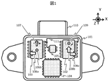
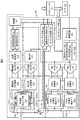
- FIG. 1 is a diagram illustrating an example of an inertial sensor.
- the sensor package unit 101 includes a first composite inertial sensor 102, a second composite inertial sensor 103, a microcontroller (microcomputer or microprocessor) 104, and a power supply regulator IC (Integrated Circuit). ) 105.
- a microcontroller microcomputer or microprocessor
- IC Integrated Circuit
- the first composite inertial sensor 102 includes a first acceleration detection axis 108a having acceleration sensitivity in the X positive direction in FIG. 1, a second acceleration detection axis 108b having acceleration sensitivity in the Y positive direction in FIG.
- a first angular velocity detection axis 109 having angular velocity sensitivity in the positive direction (Yaw) around one Z axis is provided.
- the second composite inertial sensor 103 includes a third acceleration detection axis 106a having acceleration sensitivity in the X negative direction in FIG. 1 and a fourth acceleration detection axis 106b having acceleration sensitivity in the Z positive direction in FIG. , A second angular velocity detection axis 107 having angular velocity sensitivity in the positive direction (Roll) around the Y axis in FIG.
- the first composite inertia sensor 102 and the second composite inertia sensor 103 are so-called three-axis detection sensors each having two acceleration detection axes and one angular velocity detection axis.
- a state in which a sensor having a plurality of detection axes is sealed with one package by a packaging technique such as a transfer mold package or a pre-mold package may be referred to as a “sensor module”. That is, in this embodiment, two three-axis sensor modules are mounted on the sensor package unit 101. It can be said that the sensor module is the smallest unit on which the sensor is mounted.
- the power supply regulator IC 105 converts the power supply voltage supplied from the connector 110 into a voltage suitable for the first composite inertial sensor 102 and the second composite inertial sensor 103, and supplies it through the wiring 111. That is, the first composite inertia sensor 102 and the second composite inertia sensor 103 are supplied with power from the same power regulator IC 105.
- the microcontroller 104 is connected to the first composite inertial sensor 102 and the second composite inertial sensor 103 by wiring (not shown) of a printed circuit board and the like, and is connected to the connector 110. 2, the measurement result (output result) of the composite inertial sensor 103 and information on the attitude of the sensor package unit 101 based on the measurement result are output through the connector 110.
- the signal processing for calculating the content and posture of the output signal will be described later.
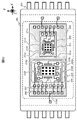
- FIG. 2 is a top view showing an example of the first composite inertial sensor 102 (sensor module).
- the first composite inertial sensor 102 includes a package 201, an external electrode 203, a signal processing integrated circuit chip (LSI) 204, an acceleration detection element chip 205, an angular velocity detection element chip 206, a pad 207, and a bonding wire 208.
- the pad 207 and the angular velocity detection element chip 206 are connected by wiring.
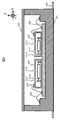
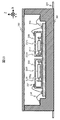
- FIG. 3 is a side view showing an example of the first composite inertial sensor 102.
- the package 201 includes a package lid 202 that is omitted in FIG. 1 and is an exterior that protects the semiconductor chip and the like that is included, and is, for example, a pre-mold package.
- a structure in which a cavity is filled with a thermosetting resin to form a package may be used.
- the output of the package 201 alone is the output of the biaxial acceleration and the monoaxial angular velocity. Output of the module.
- the signal processing integrated circuit chip 204 is fixed to the cavity in the package 201 with an adhesive (not shown) or the like, and the acceleration detection element chip 205 and the angular velocity detection element chip 206 are respectively attached to the signal processing integrated circuit chip 204. (Not shown) or the like.
- the signal processing integrated circuit chip 204, the acceleration detection element chip 205, and the angular velocity detection element chip 206 fixed in the package 201 are electrically connected through the pads 207.
- acceleration detection element chip 205 and signal processing integrated circuit chip 204 detect and process acceleration will be described.
- a first detection element 211 for detecting acceleration and a second detection element 212 are arranged with detection axes orthogonal to each other. For this reason, the acceleration detection element chip 205 can detect biaxial acceleration.
- the 1st detection element 211 and the 2nd detection element 212 are the parts enclosed with the broken line in FIG.
- the first detection element 211 is an element that detects the acceleration in the Y direction in FIG. 2, and a spring mass system is constructed in which the detection mass portion 211c is suspended from the anchor portion 211a through the spring portion 211f.
- a spring mass system is constructed in which the detection mass portion 211c is suspended from the anchor portion 211a through the spring portion 211f.
- m mass of the detection mass unit 211c
- a applied acceleration
- k The spring constant of the spring part 211f
- x Displacement according to Equation 1 of the displacement amount occurs.
- the second detection element 212 has the same structure as the first detection element 211, but the detection axis is different, and therefore the arrangement of the detection electrodes is different.
- a detection element 210 for detecting the angular velocity is arranged in the angular velocity detection element chip 206.
- the detection element 210 is a part surrounded by a broken line in FIG. 2 and is an element that detects an angular velocity around the Z axis in FIG. 2, and a spring mass in which the detection mass part 210f is suspended from the anchor part 210c through the spring part 210g.
- a system is constructed.
- the detection mass unit 210f has a constant frequency and vibration in the Y direction in FIG. 2 by the AC signal applied from the signal processing integrated circuit chip 204 to the capacitor formed by the detection mass unit 210f and the drive electrode 210b. Vibrates with amplitude (drive vibration). In order to maintain a constant vibration frequency and vibration amplitude, a drive monitor electrode 210a is provided separately, and the vibration frequency and vibration amplitude in the Y direction are input to the signal processing integrated circuit chip 204 as capacitance changes. Details of the signal processing integrated circuit chip 204 relating to driving vibration will be described later.
- the signal processing integrated circuit chip 204 obtains the displacement in the X direction generated by the Coriolis force as a change in capacitance between the detection mass unit 210f and the detection electrode 210d, and calculates the angular velocity.
- the amount of displacement generated here is expressed by an expression similar to Expression 1, but in actuality, the expression depends on the sealing pressure of the angular velocity detection element chip 206, the frequency in the driving direction, and the frequency in the detection direction. . Description of the details of this equation is omitted.
- the signal processing integrated circuit chip 204 that electrically obtains this change in capacitance will be described later.
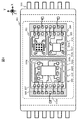
- FIG. 4 is a top view showing an example of the second composite inertial sensor 103 (sensor module).
- the second composite inertia sensor 103 includes a package 301, an external electrode 303, a signal processing integrated circuit chip 304, an acceleration detection element chip 305, an angular velocity detection element chip 306, a pad 307, and a bonding wire 308.
- the pad 307 and the angular velocity detection element chip 306 are connected by wiring.
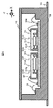
- FIG. 5 is a side view showing an example of the second composite inertial sensor 103.
- the package 301 includes a package lid 302 that is omitted in FIG. 4.
- the structure of the package 301 is the same as the structure of the package 201 shown in FIGS. Since the package 301 includes an acceleration detection element chip 305 and an angular velocity detection element chip 306, the output of the package 301 alone is a biaxial acceleration and a monoaxial angular velocity output, and the output of the triaxial detection module become.
- a first detection element 311 for detecting acceleration and a second detection element 312 are arranged with orthogonal detection axes. For this reason, the acceleration detection element chip 305 can detect biaxial acceleration. Note that the first detection element 311 and the second detection element 312 are portions surrounded by broken lines in FIG.
- the first detection element 311 is an element that detects the acceleration in the Y direction in FIG. 4 and has the same structure as the first detection element 211, and thus the description thereof is omitted.
- the second detection element 312 is an element for detecting the acceleration in the Z direction of FIG. 4, and a spring mass system is constructed in which the detection mass portion 312c is suspended from the anchor portion 312a through the spring portion 312f.
- the detection mass portion 312c is hidden behind the out-of-plane electrode 312b, and thus is illustrated in FIG.
- a displacement according to Equation 1 occurs.
- the second detection element 312 is provided with an out-of-plane electrode 312b in the Z direction of the acceleration detection element chip 305 as shown in FIG. Since a change in the gap between the detection mass unit 312c and the out-of-plane electrode 312b causes a change in capacitance, the signal processing integrated circuit chip 204 electrically obtains this change in capacitance and calculates acceleration. This detailed configuration will be described later.
- a detection element 310 for detecting the angular velocity is arranged.
- the detection element 310 is a portion surrounded by a broken line in FIG. 4 and is an element that detects an angular velocity around the X axis in FIG. 4.
- a system is constructed. Note that FIG. 4 shows the detection mass portion 310f hidden behind the out-of-plane electrode 310d, and thus is shown in FIG.
- the detection element 310 is provided with an out-of-plane electrode 310d as shown in FIG. 5, and the angular velocity detection element chip 306 is connected to the detection mass portion 310f and the out-of-plane. The change in capacitance between the electrodes 310d is obtained, and the angular velocity is calculated.
- FIGS. 2 to 4 show examples in which two detection electrodes 211b and 210d and two out-of-plane electrodes 312b and 310d are provided for the detection mass portions 211c, 210f, 312c, and 310f.
- One electrode may be provided as long as a change in capacitance can be obtained.
- the signal processing integrated circuit chip 204 of the first composite inertial sensor 102 is supplied with the power supplied to the sensor package unit 101 via the connector 110 adjusted to a predetermined voltage by the power regulator IC 105.
- one power regulator IC 105 supplies power to the second composite inertia sensor 103 in addition to the first composite inertia sensor 102 through the same wiring 111 as shown in FIG.
- the voltage of the supplied power is further adjusted by the LSI regulator unit 502 in the signal processing integrated circuit chip 204 and used as an analog unit reference voltage of the signal processing integrated circuit chip 204.
- the analog unit reference voltage includes, for example, an oscillator 503, a carrier generation unit 504, a drive signal generation unit 505, a drive side CV conversion unit 508, a drive side ADC unit 509, a detection side CV conversion unit 513, a detection side ADC unit 514, and Y 6 is supplied to the side CV conversion unit 516, the Y side ADC unit 517, the X side CV conversion unit 518, the X side ADC unit 519, the temperature sensor 522, and the carrier generation unit 524 as indicated by the bold lines in FIG. preferable.
- the signal processing integrated circuit chip 204 of the first composite inertial sensor 102 does not include the LSI regulator unit 502, and the power supplied from the power regulator IC 105 may be directly supplied to each unit in the signal processing integrated circuit chip 204. Good.
- the signal processing integrated circuit chip 204 generates an AC signal having a frequency of about several hundreds KHz by the oscillator 503.
- the AC signal is adjusted to a predetermined voltage level by the carrier generation unit 524, and is applied to the detection mass unit 211c of the acceleration detection element chip 205 through the pad 207 and the bonding wire 208.
- This AC signal is called a carrier signal.
- the carrier signal applied to the detection mass unit 211c is an AC signal
- the capacitance between the detection mass unit 211c and the detection electrodes 211b-1 and 211b-2 changes due to the application of acceleration
- the detection electrode 211b- A change occurs in the alternating current of 1,211b-2.
- the capacitance is converted into a voltage signal by the CV conversion unit 516 and converted into a digital signal through the ADC (Analog-Digital Converter) unit 517.
- a carrier signal is also applied to the detection mass unit 212c of the acceleration detection element chip 205 from the carrier generation unit 524, and it is assumed that the change in the alternating current of the detection electrodes 212b-1 and 212b-2 is a change in capacitance.
- the capacitance is converted into a voltage signal by the CV conversion unit 518 and converted into a digital signal through the ADC unit 519.
- the digital signal converted by the ADC unit 517 and the ADC unit 519 is input to the correction circuit 521.
- the correction content is stored in the memory 520 in advance, and the correction circuit 521 corrects offset and sensitivity according to the correction content of the memory 520 or performs temperature dependence compensation according to the output of the temperature sensor 522.
- Information of acceleration detected outside the first composite inertial sensor 102 is output through a digital communication circuit 523 such as SPI (Serial Peripheral Interface) communication.
- SPI Serial Peripheral Interface
- signal processing for angular velocity detection in the signal processing integrated circuit chip 204 will be described.
- To detect the angular velocity it is necessary to vibrate the detection mass unit 210f with a constant frequency and amplitude.
- the signal processing integrated circuit chip 204 uses the oscillator 503 to generate an AC signal that is a drive signal for vibrating the detection mass unit 210f.
- the oscillator 503 output to the carrier generation unit 524 for acceleration detection is also used to generate an AC signal for angular velocity detection, but is a separate body independent of the oscillator for acceleration detection. It may be an oscillator.
- a frequency divider or a multiplier may be provided at the output of the oscillator 503 to generate each AC signal.
- the AC signal output from the oscillator 503 is amplified to a predetermined voltage by the drive signal generation unit 505 and further applied to the drive electrode 210b-2 of the angular velocity detection element chip 206 through the gain adjustment unit 506. Further, the AC signal obtained by inverting the phase of the output of the gain adjusting unit 506 by the phase inverter 507 is applied to the drive electrode 210b-1. By applying these AC signals, electrostatic force is generated, and the detection mass unit 210f vibrates.
- the oscillator 503 In order to detect the amplitude and frequency of this vibration, the oscillator 503 generates an AC signal having a frequency of about several hundreds KHz. This frequency may be the same as or different from the carrier signal for capacitance detection. When the frequencies are the same, the circuit configuration becomes simple, but signal coupling may occur. Therefore, it is preferable to use different frequencies.
- the AC signal output from the oscillator 503 is adjusted to a predetermined voltage level by the carrier generation unit 504 and applied to the detection mass unit 210f of the angular velocity detection element chip 206 through the pad 207 and the bonding wire 208.
- This AC voltage signal is called a carrier signal. Since the carrier signal applied to the detection mass unit 210f is an AC signal, the capacitance between the detection mass unit 210f and the drive monitor electrodes 210a-1 and 210a-2 changes when the detection mass unit 210f is displaced. A change occurs in the alternating current of the drive monitor electrodes 210a-1 and 210a-2.
- the capacitance is converted into a voltage signal by the CV conversion unit 508 and sent to the synchronous detection unit 510 via the ADC unit 509.
- the synchronous detection unit 510 extracts two of the phase difference between the driving vibration of the detection mass unit 210f and a predetermined frequency, and the amplitude component of the displacement of the detection mass unit 210f, and outputs the extracted phase difference to the frequency control unit 511. Then, the extracted amplitude component is output to the amplitude control unit 512.
- the frequency control unit 511 outputs a control signal to the oscillator 503 so that the frequency of the drive vibration matches a predetermined frequency based on the phase difference from the drive vibration of the detection mass unit 210f.
- the amplitude control unit 512 outputs a control signal to the gain adjustment unit 506 so as to maintain a predetermined drive amplitude of the detection mass unit 210f. With these two control signals, the driving vibration of the detection mass unit 210f maintains a constant amplitude and a constant frequency.
- the displacement of the detection mass portion 210f with respect to the detection electrodes 210d-1 and 210d-2 occurs due to the Coriolis force.
- the capacitance of the detection mass unit 210f and the detection electrodes 210d-1 and 210d-2 is changed. Since the carrier signal is applied from the carrier generation unit 504 to the detection mass unit 210f, the electrostatic capacity is converted into a voltage signal by the CV conversion unit 513 and sent to the detection unit 515 through the ADC unit 514.
- the detection unit 515 extracts the amplitude component of the displacement of the detection mass unit 210f by the synchronous detection process, and calculates the force applied to the detection mass unit 210f, that is, the Coriolis force.
- the calculated Coriolis force is a force proportional to the applied angular velocity as shown in Equation 2, and the other coefficients are constants, and may be referred to as the detected applied angular velocity.
- the detected applied angular velocity is offset / gain adjusted by the correction circuit 521 or compensated for the temperature dependence according to the output of the temperature sensor 522, and then out of the first composite inertial sensor 102 through the digital communication circuit 523. Is output.
- the frequency control unit 511 controls the drive signal so that the resonance frequency of the detection mass unit 210f is generally the same as the natural frequency.
- the first composite inertial sensor 102 may be a circuit that operates with a single power source, or may be a circuit that operates with a plurality of voltage power sources. In the case of a circuit that operates with a single power supply, the power supply regulator IC 105 and the LSI regulator unit 502 may output one voltage as a power supply.
- an analog signal in a state where no acceleration or angular velocity is applied is half of the power supply voltage. It may be a voltage.
- the analog signal representing the positive direction may be a voltage larger than half the power supply voltage, and the analog signal representing the negative direction may be a voltage smaller than the half of the power supply voltage.
- the information on the acceleration and angular velocity of the digital communication circuit 523 includes information on the positive direction and information on the negative direction. For example, based on the two's complement expression, the polarity has a positive value as a positive value and a negative direction as a negative value. May be included. Further, the digital communication circuit 523 may receive a data request from outside the first composite inertial sensor 102 and transmit data on acceleration or angular velocity information at the time of receiving the data request. In particular, it may receive a data request from the microcontroller 104 and send data to the microcontroller 104.
- the microcontroller 104 outputs a total biaxial angular velocity output obtained from the first composite inertial sensor 102 and the second composite inertial sensor 103, and a triaxial acceleration output (however, the uniaxial acceleration in the three axes is two composites). Obtained from the inertial sensor), and the attitude of the sensor package unit 101 is calculated from these pieces of information.
- the microcontroller 104 calculates the initial posture using the acceleration sensor output and the inverse trigonometric function, for example, and the subsequent posture change is a relative change obtained by the time integral of the angular velocity.
- Signal processing using is performed.
- a filtering technology that always uses acceleration and angular velocity values such as the so-called Kalman filter (Kalman filter) is implemented, and the sensor error corresponding to an application called a complementary filter (Complemental filter) is directly estimated.
- the signal processing for obtaining the posture may be performed by estimating.
- each of the two three-axis compound inertial sensors has a common detection axis. That is, in the example of FIG. 1, the first acceleration detection axis 108a of the first composite inertial sensor 102 and the third acceleration detection axis 106a of the second composite inertial sensor 103 are overlapped with different detection axes (X).
- the first composite inertia sensor 102 and the second composite inertia sensor 103 are arranged so as to be an axis.
- the signal of the first acceleration detection axis 108a and the signal of the third acceleration detection axis 106a are combined to improve the signal quality (SNR, Signal Noise Ratio) calculated as the X-axis acceleration.
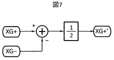
- the microcontroller 104 performs, for example, a difference calculation between the signal of the first acceleration detection axis 108a and the signal of the third acceleration detection axis 106a. As shown in FIG. 7, the difference calculation is performed by setting the output of the first acceleration detection axis 108a and the output of the third acceleration detection axis 106a as a signal XG + and a signal XG-, respectively, and inverting the polarity of the signal XG-. Two signals may be added and halved to obtain signal XG + ′.
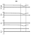
- the noise factor (common noise) common to the first acceleration detection axis 108a and the third acceleration detection axis 106a is in phase with the signal XG + and the signal XG- which are the respective sensor outputs. Appears (common mode noise).
- the microcontroller 104 adds one of the signals of the axes measuring the same physical quantity having the opposite sensitivity while inverting the polarity, a signal with the common noise canceled can be obtained as the signal XG + ′.
- An example of common noise in this embodiment is that the power supply regulator IC 105 is common to the first composite inertial sensor 102 and the second composite inertial sensor 103, and therefore, when the voltage output from the power supply regulator IC 105 varies, This noise appears in the output of the first composite inertial sensor 102 and the output of the second composite inertial sensor 103.
- Voltage is a voltage of a single power supply, and when the voltage temporarily decreases, the voltage of the signal XG + that is an analog signal also decreases according to the power supply voltage. Since “0” of the signal XG ⁇ that is an analog signal is a voltage that is half of the power supply voltage, the voltage of the signal XG ⁇ changes so that the difference from “0” becomes large, as shown in FIG.
- the influence of external electromagnetic waves or the like generated according to the installation environment of the sensor package unit 101 appears as common noise at the outputs of the first composite inertia sensor 102 and the second composite inertia sensor 103 that are close to each other in physical distance. Canceling these common noises is suitable for improving the signal quality of the acceleration sensor, and is therefore beneficial for improving the accuracy of posture calculation.
- the output of the first composite inertial sensor 102 and the output of the second composite inertial sensor 103 are not limited to the power source, the external electromagnetic wave, etc.
- Circuit noise related to displacement and detection occurs as uncorrelated noise.
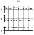
- the microcontroller 104 reverses the polarity of one of the signals of the same physical quantity that have the opposite sensitivity and adds the signals, so the signal component is doubled and the noise component is The signal quality of the signal XG + 'is improved by a factor of ⁇ 2 (3dB).
- the first acceleration detection axis 108a and the third acceleration detection axis 106a are configured to measure the same physical quantity (including the axis) having opposite sensitivities, but have the same sensitivity and common noise. 7 appears in the opposite polarity direction, or when there is uncorrelated noise with the same sensitivity, the process shown in FIG. May be replaced. Furthermore, the same signal processing may be applied to the temperature sensor 522 mounted on the first composite inertial sensor 102 shown in FIG. 6, and the same signal processing is performed for the temperature sensors of other composite inertial sensors. You may give it.
- the same physical quantity (including the axis) with the opposite sensitivity is measured even when performing signal processing to detect the posture of the target by always using the output of the acceleration sensor and the output of the angular velocity sensor as filter inputs as in the Kalman filter.
- the filter By inputting the outputs of both the first acceleration detection axis 108a and the third acceleration detection axis 106a to the filter, it is possible to improve posture detection accuracy.
- ⁇ Gyro is a posture calculated by time integration of the angular velocity sensor
- ⁇ XG + and ⁇ XG ⁇ are postures calculated from the output of the acceleration sensor by an inverse trigonometric function.
- This complementary filter estimates and compensates for the time integration error of the angular velocity sensor.
- the signals ( ⁇ Gyro, ⁇ XG ⁇ ) input to the complementary filter can be increased.
- a plausible ⁇ Gyro error is estimated from a plurality of input signals. If independent signal components are included in ⁇ XG + and ⁇ XG ⁇ , the error estimation accuracy of the complementary filter can be improved.
- the microcontroller 104 uses a sample rate that is twice or more faster than the band of the acceleration signal detected on each of the first acceleration detection axis 108a and the third acceleration detection axis 106a that measure the same physical quantity (including the axis).
- data is read from each of the first composite inertial sensor 102 and the second composite inertial sensor 103.
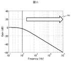
- FIG. 11 shows a frequency response graph when the acceleration signal detected by the third acceleration detection axis 106a has a 100 Hz band as an example. That is, a frequency of 100 Hz at which a response decrease of at least ⁇ 3 dB is set as an upper limit of a band of a signal detected by the third acceleration detection axis 106a.
- the sampling rate (reading speed, output to the composite inertial sensor) in the microcontroller 104 is included. If the data request transmission interval is less than 200 Hz, the signal components representing acceleration, common noise, and uncorrelated noise signal waveforms may be distorted by the aliasing phenomenon, and the operation described above may not be achieved. There is. For this reason, it is desirable that the sample rate be 200 Hz or more indicated by an arrow 701 in FIG.
- the signal quality improvement utilizing the first acceleration detection axis 108a and the third acceleration detection axis 106a that measure the same physical quantity (including the axis) having the opposite sensitivity obtained in this embodiment is particularly new.
- a detection axis that necessarily overlaps in a configuration using two three-axis sensor modules that provide functions as an acceleration / angular velocity sensor alone is not obtained. It may be used.
- highly accurate acceleration sensor output that is, detection of the absolute posture without adding special costs (hardware cost, development period, installation area).
- FIG. 12 is a top view illustrating an example of the composite inertial sensor of the second embodiment
- FIG. 13 is a side view illustrating an example of the composite inertial sensor of the second embodiment.
- the spring part 211f has a degree of freedom by which the detection mass part 211c can be displaced on both the X axis and the Y axis in FIG. 12, and the displacement when a static linear acceleration in the X direction in FIG. 12 is applied is detected.
- the displacement detected by the electrode 211e and when a static linear acceleration in the Y direction in FIG. 12 is applied is detected by the detection electrode 211b.
- the first detection element 211 performs biaxial acceleration detection.
- the first composite inertial sensor 102 of the sensor package unit 101 shown in FIG. 1 has the structure shown in FIGS.
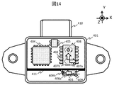
- FIG. 14 is a diagram illustrating an example of the inertial sensor of the third embodiment.
- the inertial sensor according to the third embodiment includes a first composite inertia sensor 402, a second composite inertia sensor 403, a microcontroller 404, and a power supply regulator IC 405 in a sensor package unit 401.
- the power regulator IC 405 supplies power to the first composite inertia sensor 402 and the second composite inertia sensor 403.
- the inertial sensor of the third embodiment is different from the inertial sensor of the first embodiment, and the first composite inertial sensor 402 and the second composite inertial sensor 403 are substantially rectangular parallelepipeds having the same shape, and the same A composite inertial sensor having the same detection axis with respect to the surface and having the same specifications physically and electrically, but the surface on which the first composite inertial sensor 402, the microcontroller 404, and the power supply regulator IC 405 are arranged (XY plane)
- the second composite inertial sensor 403 is disposed at a step 411 (XZ plane) that is substantially perpendicular to ().
- the first composite inertial sensor 402 includes a first acceleration detection axis 407a having acceleration sensitivity in the X positive direction in FIG. 14 and a second acceleration detection having acceleration sensitivity in the Y positive direction in FIG.
- the shaft 407b and the first angular velocity detection shaft 408 having angular velocity sensitivity in the positive direction (Yaw) around the Z-axis in FIG. 14 are provided
- the second composite inertial sensor 403 has a negative X direction in FIG. 14 has a third acceleration detection axis 408a having an acceleration sensitivity, a fourth acceleration detection axis 408b having an acceleration sensitivity in the positive Z direction in FIG. 14, and an angular velocity sensitivity in the positive direction (Roll) around the Y axis in FIG.
- the second angular velocity detection axis 409 is provided.
- the inertial sensor shown in FIG. 14 can detect accelerations in the X direction, Y direction, and Z direction, can detect the angular velocities of Yew and Roll, and is in the X positive direction as in the example of the inertial sensor shown in FIG. And the negative X-direction acceleration can be detected independently.
- the signal quality improvement effect shown in the first embodiment can be obtained by calculating the difference between the first acceleration detection axis 407a and the third acceleration detection axis 408a that measure the same physical quantity having the opposite sensitivity. .
- first compound inertia sensor 402 and the second compound inertia sensor 403 are three-axis sensor modules having the same specifications, the amount of variation in common noise generated following the variation of the power supply regulator IC 405 and the sensitivity are affected.
- temperature dependence bias, sensitivity
- a useful effect as Example 3 can be obtained.
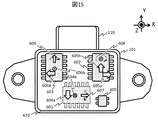
- FIG. 15 is a diagram illustrating an example of the inertial sensor of the fourth embodiment.
- the inertial sensor of the fourth embodiment includes a first composite inertial sensor 601, a second composite inertial sensor 602, a third composite inertial sensor 603, a microcontroller (not shown), a power source, and the like.
- a regulator IC 605 is included. The power regulator IC 605 supplies power to the first composite inertia sensor 601, the second composite inertia sensor 602, and the third composite inertia sensor 603.
- the board 610 is a double-sided board arranged so as to be the XY plane in the sensor package unit 101, and the second composite inertia sensor 602 and the third composite inertia sensor 603 are mounted on the same face of the board 610.
- the first combined inertial sensor 601 is mounted on the back side of the substrate 610 on which the second combined inertial sensor 602 and the third combined inertial sensor 603 are mounted.
- the first compound inertia sensor 601 is a compound inertia sensor, that is, a sensor module having the same specifications as the third compound inertia sensor 603.
- the first acceleration detection shaft 604a of the first composite inertial sensor 601 and the second acceleration detection shaft 605b of the second composite inertial sensor 602 have opposite sensitivities. This corresponds to the acceleration detection axis that measures the same physical quantity. Further, the second acceleration detection axis 604b of the first composite inertial sensor 601 and the second acceleration detection axis 606b of the third composite inertial sensor 603 correspond to the acceleration detection axis that measures the same physical quantity having opposite sensitivities. .
- first acceleration detection axis 605a of the second composite inertial sensor 602 and the first acceleration detection axis 606a of the third composite inertial sensor 603 correspond to the acceleration detection axis that measures the same physical quantity having the opposite sensitivity. .
- the power regulator IC 605 supplies a voltage to the composite inertial sensor related to the three axes, the effect of canceling the common noise against the power fluctuation can be obtained for the acceleration of the three axes.
- a step (not shown) is provided in the sensor package unit 101, and the first composite inertia sensor 601 and the third composite inertia are used instead of the second composite inertia sensor 602.
- a compound inertia sensor having the same specifications as the sensor 603 may be mounted on the step.
- the composite inertial sensor may have a structure of, for example, biaxial angular velocity detection and triaxial acceleration detection.
- the same effect that is, improvement in signal quality by synthesizing acceleration detection axes that measure the same physical quantity having opposite sensitivity can be obtained for three-axis acceleration.
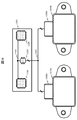
- FIG. 16 is a diagram illustrating an example of the inertial sensor of the fifth embodiment.
- Each of the sensor package units 1010a and 1010b is connected to a communication IC 1103 installed on the substrate 1102 via a communication bus 1101 connected to the connectors 1100a and 1100b.
- the microcontroller 1104 includes an MPU (Micro Processing Unit) having a higher calculation capacity than the microcontrollers 104 and 404 of the first to fourth embodiments, and mainly measures acceleration for measuring the same physical quantity in order to improve the signal quality described in the first embodiment. Signal processing using the detection axis is executed. Thereby, even if the signal processing for posture detection is a complicated procedure, it can be processed, and the advantages shown in the first embodiment can be continuously obtained.
- MPU Micro Processing Unit
- the position information acquisition module 1106 may be a module for a system that obtains absolute coordinates on the earth such as a GPS (Global Positioning System) receiver. In this case, the posture detection accuracy can be improved by correcting the gravity that varies depending on the latitude on the earth by the microcontroller 1104.
- the sensor package units 1010a and 1010b may be any of the sensor package units 101 and 401 described in the first to fourth embodiments.
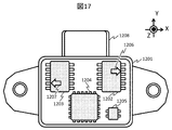
- FIG. 17 is a diagram illustrating an example of the inertial sensor according to the sixth embodiment.
- the inertial sensor of the sixth embodiment includes a first inertial sensor 1202, a second inertial sensor 1203, a microcontroller 1204, and a power supply regulator IC 1205 in the sensor package unit 1201.
- the first inertial sensor 1202 includes a first acceleration detection axis 1206 having acceleration sensitivity in the X positive direction in FIG. 17, and the second inertial sensor 1203 has a second acceleration sensitivity in the X negative direction in FIG.
- the acceleration detection axis 1207 is provided.
- a power supply IC 1205 supplies power to the first inertial sensor 1202 and the second inertial sensor 1203.
- the inertial sensor of this embodiment is an angular velocity sensor
- the initial inclination cannot be obtained.
- two outputs for measuring the same angular velocity having opposite sensitivities can be obtained.
- the relative inclination can be calculated with high accuracy.
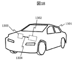
- FIG. 18 is a diagram illustrating an example of an automobile 1301.
- the automobile 1301 of the seventh embodiment includes a first sensor package part 1302, a second sensor package part 1303, and a communication path 1304 that connects them in the automobile 1301.
- the first sensor package unit 1302 includes the first composite inertial sensor 102 shown in FIG. 1, the microcontroller 104, and the power supply regulator IC 105.
- the first composite inertial sensor 102 of the first sensor package unit 1302 includes , A first acceleration detection axis 108a having acceleration sensitivity in the X positive direction in FIG. 1, a second acceleration detection axis 108b having acceleration sensitivity in the Y positive direction in FIG. 1, and a positive direction around the Z axis in FIG. Yaw) includes a first angular velocity detection axis 109 having angular velocity sensitivity.
- the second sensor package unit 1303 is an inertial sensor installed in the automobile 1301 and intended for uses other than the attitude detection of the automobile. Then, at least one acceleration detection axis of the inertial sensor of the second sensor package unit 1303 includes an inertial sensor that measures the same physical quantity having a sensitivity opposite to that of the first acceleration detection axis 108a or the second acceleration detection axis 108b. .
- the microcontroller 104 of the first sensor package unit 1302 acquires the acceleration detected from the second sensor package unit 1303 via the communication path 1304, and detects the acceleration detected in the first sensor package unit 1302. Improve signal quality by combining.
- the obtained acceleration may be used for controlling driving of the automobile 1301.
- the present embodiment can be used for an apparatus that performs posture control using an inertial sensor, such as a robot or a drone, other than a car.
Landscapes
- Physics & Mathematics (AREA)
- General Physics & Mathematics (AREA)
- Engineering & Computer Science (AREA)
- Radar, Positioning & Navigation (AREA)
- Remote Sensing (AREA)
- Gyroscopes (AREA)
- Control Of Position, Course, Altitude, Or Attitude Of Moving Bodies (AREA)
Abstract
複数の検出軸での検出結果を出力する物理センサを複数備えたセンサ装置であって、複数の検出軸のそれぞれは、検出軸にそった検出方向があり、複数の前記物理センサの中の第1の物理センサは、前記第1の物理センサの複数の検出軸の中に第1の検出軸を有し、複数の前記物理センサの中の第2の物理センサは、前記第2の物理センサの複数の検出軸の中に第2の検出軸を有し、前記第1の検出軸と前記第2の検出軸は重複し、前記第1の検出軸の検出方向と前記第2の検出軸の検出方向は逆方向となるように、前記第1の物理センサと前記第2の物理センサが配置される。
Description
本発明は、センサ装置および自動運転車両に関するものである。
近年、自動車の安全支援・自動運転、ロボットの制御、そしていわゆるドローン等と呼ばれる自律飛行装置等のアプリケーションが普及しつつある。これらのアプリケーションでは、対象の姿勢や角度を検出することがその制御に重要である。このため、角速度・加速度を検出する慣性センサがこれらのアプリケーションで重要なコンポーネントとなっている。
さらに今日ではMEMS(Micro Electro Mechanical Systems)と呼ばれる、半導体の微細加工技術を用いて作製される微小機械デバイスによって、実用レベルの確度・精度を有する慣性センサが市販されるようになってきた。MEMSで作製される慣性センサは、半導体プロセスによって作製されるため、センサエレメント(慣性力を検出する機械構造)を並列かつ大量に作ることができる。このことが、従来高価格であった慣性センサの低価格化をもたらし、前述のようなアプリケーションを一般的にする原動力となっている。
一般に、慣性センサを用いた姿勢の検出原理は大きく2つある。1つ目は、重力が垂直方向に常に1G(9.8m/s2)であることを利用し、X、Y、Z方向それぞれの感度を持つ加速度センサから、どちらの方向に重力がかかっているかをみることで、傾き方向、すなわち姿勢を得る方法である。この原理は、対象が加速していたり、回転運動をして遠心力が加速度センサにかかるような状態であったりする場合は、その慣性力(外乱)によって、誤差を生じる。
もうひとつ姿勢検出原理として、角速度センサを時間積分して、積分開始時点からの角度変化量を計算するものがある。この検出原理には、対象が加速していたり、回転運動による遠心力がセンサに印加されたりしていても、本質的にこれらの影響を受けない。これは、加速度センサを用いた姿勢の検出原理にはない特徴である。
しかし、時間積分によって姿勢を検出する原理では、絶対姿勢を得ることができず、得られるのは初期姿勢からの相対姿勢に留まる。何らかの方法で初期姿勢を定義し、相対姿勢を加算することで姿勢を得ることは可能である。しかし、積分によるバイアス誤差の積算があるため、オフセットのドリフトが大きくなり、絶対姿勢に対する誤差が時間と共に大きくなってしまう。そこで、加速度センサによって絶対姿勢の補正を適宜行う共に、角速度センサによって姿勢検出を行う、信号処理を組み合わせた計測システムが用いられることがある。
本技術分野の背景技術として、例えば特許文献1がある。特許文献1では、3軸の角速度センサと、加速度センサの、それぞれの出力をカルマンフィルタで処理し、角速度センサのオフセットドリフトを推定する慣性計測装置において、第4の角速度センサを設けることで、角速度センサのオフセットドリフトを精度よく推定する手法が開示されている。また、特許文献2では全ての検出軸に対して感度を持つ冗長な検出軸を設け、検出軸が故障した際には冗長軸で代用するという機能によって、故障耐性を高めたセンサが開示されている。
特許文献1に示されるような、角速度の積分と、加速度から姿勢角を得る構成の慣性センサについて検討した結果、以下の課題が明らかとなった。すなわち、角速度センサでは絶対姿勢を得ることができないため、角速度センサを用いて絶対姿勢を精度良く求めるには、初期姿勢を精度良く得ることが重要であり、加速度センサの高精度化が必要となる。
特許文献1に、角速度センサのオフセットドリフト等を向上する技術は開示されているが、絶対姿勢検出の精度向上に関する技術は開示されていない。また、特許文献2に開示された技術は、故障発生時の耐性を高めるものであって、やはり姿勢検出の精度向上に関する技術ではない。
例えば、加速度センサの精度向上に関しては、MEMS型に対していわゆるバルク型と呼ばれる、質量のある検出マスを有する加速度センサを用いる技術がある。しかしながら、コスト・サイズ面での負担を強いることとなるため、背景技術に記載のような、コストが原因で従来普及していなかったアプリケーションを実現するという観点においては、現実的ではない。
また、MEMS型センサにおいて、特別に検出マスの質量を大きくした検出エレメントを開発したり、大きなサイズのMOS(Metal-Oxide Semiconductor)トランジスタを検出回路に利用した低ノイズ回路を開発したりすることで、加速度センサの精度向上を図ることは可能である。しかしながら、開発のための設計コストがかかるほか、開発のための時間もかかってしまう。
本発明は、上記のような課題に鑑みてなされたものであり、物理センサの検出精度向上を目的とする。
本願において開示される発明のうち、代表的なものの概要を簡単に説明すれば、請求項に記載の構成の通りである。その1つは、複数の検出軸での検出結果を出力する物理センサを複数備えたセンサ装置であって、複数の検出軸のそれぞれは、検出軸にそった検出方向があり、複数の前記物理センサの中の第1の物理センサは、前記第1の物理センサの複数の検出軸の中に第1の検出軸を有し、複数の前記物理センサの中の第2の物理センサは、前記第2の物理センサの複数の検出軸の中に第2の検出軸を有し、前記第1の検出軸と前記第2の検出軸は重複し、前記第1の検出軸の検出方向と前記第2の検出軸の検出方向は逆方向となるように、前記第1の物理センサと前記第2の物理センサが配置されたことを特徴とする。
本発明によれば、物理センサの検出精度を向上することが可能になる。
以下の実施の形態(実施例)においては、便宜上その必要があるときは、複数のセクションまたは実施の形態に分割して説明するが、特に明示した場合を除き、それらは互いに無関係なものではなく、一方は他方の一部または全部の変形例、詳細、補足説明等の関係にある。また、以下の実施の形態において、要素の数等(個数、数値、量、範囲等を含む)に言及する場合、特に明示した場合および原理的に明らかに特定の数に限定される場合等を除き、その特定の数に限定されるものではなく、特定の数以上でも以下でもよい。
さらに、以下の実施の形態において、その構成要素(要素ステップ等も含む)は、特に明示した場合および原理的に明らかに必須であると考えられる場合等を除き、必ずしも必須のものではないことは言うまでもない。同様に、以下の実施の形態において、構成要素等の形状、位置関係等に言及するときは、特に明示した場合および原理的に明らかにそうでないと考えられる場合等を除き、実質的にその形状等に近似または類似するもの等を含むものとする。このことは、上記数値および範囲についても同様である。
以下の実施において、特に断りのない限り「加速度」と「角速度」は相互に入れ替え可能であるが、説明を簡単にするために、「加速度」と「角速度」の組み合わせとして1通りの実施例を示すこととする。
図1は、慣性センサの例を示す図である。実施例1の慣性センサでは、センサパッケージ部101に、第1の複合慣性センサ102と、第2の複合慣性センサ103と、マイクロコントローラ(マイコン、ないしはマイクロプロセッサ)104と、電源レギュレータIC(Integrated Circuit)105を有する。
第1の複合慣性センサ102は、図1のX正方向に加速度感度を持つ第1の加速度検出軸108aと、図1のY正方向に加速度感度を持つ第2の加速度検出軸108bと、図1のZ軸回り正方向(Yaw)に角速度感度を持つ第1の角速度検出軸109を備えている。
また、第2の複合慣性センサ103は、図1のX負方向に加速度感度を持つ第3の加速度検出軸106aと、図1のZ正方向に加速度感度を持つ第4の加速度検出軸106bと、図1のY軸回り正方向(Roll)に角速度感度を持つ第2の角速度検出軸107を備えている。
従って、第1の複合慣性センサ102と、第2の複合慣性センサ103は、いずれも2つの加速度検出軸と、1つの角速度検出軸を有する、いわゆる3軸検出のセンサである。このように複数の検出軸を有するセンサが、トランスファーモールドパッケージやプリモールドパッケージといったパッケージング技術によって、1つのパッケージで封止されている状態を「センサモジュール」と呼ぶこともある。すなわち、本実施例では、センサパッケージ部101に、2つの3軸センサモジュールが実装される。なお、センサモジュールはセンサの実装される最小の単位であるとも言える。
ここで、電源レギュレータIC105は、コネクタ110から供給された電源電圧を、第1の複合慣性センサ102と第2の複合慣性センサ103に適した電圧へ変換し、配線111を通じて供給する。すなわち、第1の複合慣性センサ102と、第2の複合慣性センサ103は、同一の電源レギュレータIC105から電源の供給を受ける。
マイクロコントローラ104は、第1の複合慣性センサ102および第2の複合慣性センサ103とプリント基板の配線(図示省略)等によって接続されるとともにコネクタ110に接続され、第1の複合慣性センサ102と第2の複合慣性センサ103の測定結果(出力結果)や、その測定結果に基づくセンサパッケージ部101の姿勢に関する情報を、コネクタ110を通じて出力する。この出力する信号の内容や姿勢を計算する信号処理については後述する。
図2は、第1の複合慣性センサ102(センサモジュール)の例を示す上面図である。ここで、図2のZ正方向と上とする。第1の複合慣性センサ102は、パッケージ201、外部電極203、信号処理集積回路チップ(LSI)204、加速度検出エレメントチップ205、角速度検出エレメントチップ206、パッド207、ボンディングワイヤ208からなる。そして、例えばパッド207と角速度検出エレメントチップ206は配線で接続される。
図3は、第1の複合慣性センサ102の例を示す側面図である。ここで、図3のY負方向を側方とする。パッケージ201は、図1では省略したパッケージふた202を含み、内包する半導体チップ等を保護する外装であり、例えばプリモールドパッケージである。図2に示すように、パッケージ201内に空洞(チャンバー)を有する構造の他、熱硬化樹脂によって空洞が埋められてパッケージが形成される構造であってもよい。なお、図2において、図1に示した物と同じ物には同じ符号を付す。
このように、パッケージ201には加速度検出エレメントチップ205と角速度検出エレメントチップ206が含まれるため、パッケージ201が単体でもその出力は、2軸の加速度と1軸の角速度の出力であり、3軸検出モジュールの出力となる。
パッケージ201内の空洞に、信号処理集積回路チップ204は接着剤(図示省略)等によって固定され、さらに、加速度検出エレメントチップ205と角速度検出エレメントチップ206は、信号処理集積回路チップ204にそれぞれ接着剤(図示省略)等で固定される。そして、パッケージ201内に固定された信号処理集積回路チップ204、加速度検出エレメントチップ205、角速度検出エレメントチップ206は、パッド207を通じて電気的に接続される。
まず、加速度検出エレメントチップ205と信号処理集積回路チップ204がどのように加速度を検出して処理するかについて述べる。加速度検出エレメントチップ205には、加速度を検出する第1の検出エレメント211と、第2の検出エレメント212が、直交する検出軸を有して配置されている。このため、加速度検出エレメントチップ205は2軸の加速度検出が可能である。なお、第1の検出エレメント211と第2の検出エレメント212は、図2においてそれぞれ破線で囲まれた部分である。
第1の検出エレメント211は図2のY方向の加速度を検出するエレメントであり、アンカー部211aにばね部211fを通じて検出マス部211cが懸架されるバネマス系が構築される。ここで、静的な線形の加速度が印加されると、

k:ばね部211fのばね定数、x:変位量
の式1に従った変位が発生する。
この変位は、検出マス部211cと検出電極211bとのギャップ変化をもたらし、静電容量を変化させる。信号処理集積回路チップ204は電気的にこの静電容量変化を得て、加速度を算出する。この詳細な構成については、後述する。また、第2の検出エレメント212も第1の検出エレメント211と同じ構造であるが、検出軸が異なるため、検出電極の配置が異なる。
次に、角速度検出エレメントチップ206と信号処理集積回路チップ204がどのように角速度を検出して処理するかの原理について述べる。角速度検出エレメントチップ206には、角速度を検出する検出エレメント210が配置されている。検出エレメント210は、図2において破線で囲まれた部分であって、図2のZ軸周りの角速度を検出するエレメントであり、アンカー部210cにばね部210gを通じて検出マス部210fが懸架されるバネマス系が構築される。
ここで、検出マス部210fは、検出マス部210fと駆動電極210bで構成されるコンデンサに信号処理集積回路チップ204から印加された交流信号によって、図2のY方向に、一定の振動数と振動振幅で振動する(駆動振動)。一定の振動数と振動振幅を維持するために、駆動モニタ電極210aが別途設けられ、Y方向の振動数と振動振幅が静電容量変化として信号処理集積回路チップ204に入力される。駆動振動に関する信号処理集積回路チップ204の詳細については後述する。
ここで、検出マス部210fのY方向の振動によって生じる変位速度をvと置くとき、Z軸周りの角速度Ωが印加されると、

Ω:印加角速度、v: 検出マス部210fの変位速度
の式に従ったコリオリ力が図2のX方向に発生する。
信号処理集積回路チップ204が、このコリオリ力によって発生するX方向の変位を検出マス部210fと検出電極210d間の静電容量変化として得て、角速度を算出する。なお、ここで発生する変位量は、式1に類似した式で表現されるが、実際は角速度検出エレメントチップ206の封止圧力および駆動方向の振動数、検出方向の振動数に依存した式となる。この式の詳細については説明を省略する。また、この静電容量変化を電気的に得る信号処理集積回路チップ204については後述する。
図4は、第2の複合慣性センサ103(センサモジュール)の例を示す上面図である。ここで、図4のZ正方向と上とする。第2の複合慣性センサ103は、パッケージ301、外部電極303、信号処理集積回路チップ304、加速度検出エレメントチップ305、角速度検出エレメントチップ306、パッド307、ボンディングワイヤ308からなる。そして、例えばパッド307と角速度検出エレメントチップ306は配線で接続される。
図5は、第2の複合慣性センサ103の例を示す側面図である。ここで、図5のY負方向を側方とする。パッケージ301は、図4では省略したパッケージふた302を含み、パッケージ301の構造は、図2、3に示したパッケージ201の構造と同じであるので、説明を省略する。パッケージ301には加速度検出エレメントチップ305と角速度検出エレメントチップ306が含まれるため、パッケージ301が単体でもその出力は、2軸の加速度と1軸の角速度の出力であり、3軸検出モジュールの出力となる。
加速度検出エレメントチップ305には、加速度を検出する第1の検出エレメント311と、第2の検出エレメント312が、直交する検出軸を有して配置されている。このため、加速度検出エレメントチップ305は2軸の加速度検出が可能である。なお、第1の検出エレメント311と第2の検出エレメント312は、図4においてそれぞれ破線で囲まれた部分である。第1の検出エレメント311は図4のY方向の加速度を検出するエレメントであり、第1の検出エレメント211と同じ構造であるため、説明を省略する。
第2の検出エレメント312は、図4のZ方向の加速度を検出するエレメントであり、アンカー部312aにばね部312fを通じて検出マス部312cが懸架されるバネマス系が構築される。なお、図4では、検出マス部312cが面外電極312bに隠れるため、図5に示す。ここで、静的な線形の加速度が印加されると、式1に従った変位が発生する。
この変位を静電容量の変化として得るため、第2の検出エレメント312では、図5に示すように、加速度検出エレメントチップ305のZ方向に面外電極312bが設けられている。検出マス部312cと面外電極312bとのギャップ変化が静電容量の変化をもたらすので、信号処理集積回路チップ204は電気的にこの静電容量変化を得て、加速度を算出する。この詳細な構成については、後述する。
また、図4に示す角速度検出エレメントチップ306には、角速度を検出する検出エレメント310が配置されている。検出エレメント310は、図4において破線で囲まれた部分であって、図4のX軸周りの角速度を検出するエレメントであり、アンカー部310cにばね部310gを通じて検出マス部310fが懸架されるバネマス系が構築される。なお、図4では、検出マス部310fが面外電極310dに隠れるため、図5に示す。
そして、検出マス部310fのY方向の振動によって生じる変位速度をvと置くとき、X軸周りの角速度Ωが印加されると、式2に従った力が図5のZ方向に発生する。このコリオリ力によって発生するZ方向の変位を検出するため、検出エレメント310では、図5に示すように、面外電極310dが設けられており、角速度検出エレメントチップ306は検出マス部310fと面外電極310d間の静電容量変化を得て、角速度を算出する。
なお、図2~4では、検出マス部211c、210f、312c、310fに対して、検出電極211b、210dと面外電極312b、310dをそれぞれ2つ備える例を示したが、加速度に対して十分な容量変化が得られるのであれば、各電極は1つであってもよい。
次に、第1の複合慣性センサ102の信号処理集積回路チップ204の例について図6を用いて説明する。信号処理集積回路チップ204は、コネクタ110経由でセンサパッケージ部101に供給された電源を、電源レギュレータIC105で所定の電圧に調整されて供給される。ここで、1つの電源レギュレータIC105は、図1で示したとおり同じ配線111を通じて、第1の複合慣性センサ102に加えて第2の複合慣性センサ103へも電源を供給する。
供給された電源は、信号処理集積回路チップ204内のLSIレギュレータ部502により電圧がさらに調整され、信号処理集積回路チップ204のアナログ部基準電圧として用いられる。このアナログ部基準電圧は、例えば、発振器503、キャリア生成部504、駆動信号生成部505、駆動側CV変換部508、駆動側ADC部509、検出側CV変換部513、検出側ADC部514、Y側CV変換部516、Y側ADC部517、X側CV変換部518、X側ADC部519、温度センサ522、キャリア生成部524に対して、図6の太線で示すように供給されることが好ましい。
なお、第1の複合慣性センサ102の信号処理集積回路チップ204はLSIレギュレータ部502を備えず、電源レギュレータIC105から供給される電源が信号処理集積回路チップ204内の各部へ直接に供給されてもよい。
以下に、信号処理集積回路チップ204における加速度検出の信号処理について述べる。信号処理集積回路チップ204は、発振器503で周波数数100KHz程度の交流信号を生成する。この交流信号はキャリア生成部524で所定の電圧レベルに調整され、加速度検出エレメントチップ205の検出マス部211cに、パッド207とボンディングワイヤ208を通じて印加される。この交流信号をキャリア信号と呼ぶ。
検出マス部211cに印加されるキャリア信号は交流信号であるので、検出マス部211cと検出電極211b-1、211b-2との静電容量に加速度の印加による変化があると、検出電極211b-1、211b-2の交流電流に変化が生じる。この交流電流の変化を静電容量の変化であるとして、この静電容量はCV変換部516で電圧信号に変換され、ADC(Analog-Digital Convertor)部517を通じてデジタル信号へと変換される。
また、加速度検出エレメントチップ205の検出マス部212cにもキャリア信号がキャリア生成部524から印加され、検出電極212b-1、212b-2の交流電流の変化を静電容量の変化であるとして、この静電容量はCV変換部518で電圧信号に変換され、ADC部519を通じてデジタル信号へと変換される。そして、ADC部517とADC部519で変換されたデジタル信号は補正回路521に入力される。
メモリ520には補正内容があらかじめ格納されており、補正回路521はメモリ520の補正内容に従ってオフセットや感度の補正を行ったり、温度センサ522の出力に応じた温度依存性補償を行ったりした後、SPI(Serial Peripheral Interface)通信等のデジタル通信回路523を通じて第1の複合慣性センサ102外へ検出した加速度の情報を出力する。
次に、信号処理集積回路チップ204における角速度検出の信号処理について述べる。角速度の検出には、検出マス部210fを一定の周波数および振幅で振動させる必要がある。これを実現するため、信号処理集積回路チップ204は、発振器503を用いて、検出マス部210fを振動させるための駆動信号となる交流信号を生成する。
図6の例では、加速度検出のためにキャリア生成部524へ出力する発振器503を、角速度検出のための交流信号の生成にも兼用するが、加速度検出のための発振器とは独立な別個体の発振器であってもよい。加速度検出と角速度検出とで異なる周波数の交流信号が使用される場合は、発振器503の出力に図示を省略した分周器や逓倍器が備えられて、それぞれの交流信号が生成されてもよい。
発振器503から出力された交流信号は、駆動信号生成部505にて所定の電圧に増幅され、さらにゲイン調整部506を通じて、角速度検出エレメントチップ206の駆動電極210b-2へ印加される。また、ゲイン調整部506の出力が位相反転器507で位相反転された交流信号は、駆動電極210b-1へ印加される。これらの交流信号の印加によって静電力が生じ、検出マス部210fは振動する。
この振動の振幅と周波数を検出するため、発振器503は周波数が数100KHz程度の交流信号を生成する。この周波数は静電容量検出のためのキャリア信号と同じであっても、異なっていてもよい。周波数が同じである場合は、回路構成が単純になるものの、信号カップリングの発生する可能性があるため、異なる周波数を用いる方が好ましい。
発振器503から出力された交流信号はキャリア生成部504で所定の電圧レベルに調整され、角速度検出エレメントチップ206の検出マス部210fに、パッド207とボンディングワイヤ208を通じて印加される。この交流電圧信号をキャリア信号と呼ぶ。検出マス部210fに印加されるキャリア信号は交流信号であるので、検出マス部210fに変位があると、検出マス部210fと駆動モニタ電極210a-1、210a-2との静電容量が変化し、駆動モニタ電極210a-1、210a-2の交流電流に変化が生じる。
この交流電流の変化を静電容量の変化であるとして、この静電容量はCV変換部508で電圧信号に変換され、ADC部509を経て同期検波部510に送られる。同期検波部510は、検出マス部210fの駆動振動と所定の周波数との位相差と、検出マス部210f変位の振幅成分の2つを抽出し、抽出された位相差を周波数制御部511へ出力し、抽出された振幅成分を振幅制御部512へ出力する。
周波数制御部511は、検出マス部210fの駆動振動との位相差に基づいて、駆動振動の周波数と所定の周波数とが一致するよう、発振器503へ制御信号を出力する。また、振幅制御部512は、あらかじめ定められた検出マス部210fの駆動振幅を維持するよう、ゲイン調整部506へ制御信号を出力する。これら2つの制御信号によって、検出マス部210fの駆動振動は一定の振幅と一定の周波数が維持される。
角速度検出エレメントチップ206の検出マス部210fの駆動振動が維持されている状態で、角速度が印加されると、コリオリ力によって検出電極210d-1、210d-2に対する検出マス部210fの変位が発生し、検出マス部210fと検出電極210d-1、210d-2との静電容量に変化をもたらす。キャリア生成部504から検出マス部210fにキャリア信号が印加されているため、静電容量はCV変換部513で電圧信号に変換され、ADC部514を通じて検出部515へ送られる。
検出部515は、同期検波処理によって検出マス部210fの変位が持つ振幅成分を抽出して、検出マス部210fに加わった力すなわちコリオリ力を算出する。算出されたコリオリ力は、式2に示すとおり印加角速度に比例する力であり、他の係数は定数であるので、検出した印加角速度と言ってよい。検出した印加角速度は、補正回路521でオフセット・ゲイン調整を行ったり、温度センサ522の出力に応じた温度依存性補償を行ったりした後、デジタル通信回路523を通じて第1の複合慣性センサ102外へ出力される。
ところで、駆動振幅が大きくなり駆動方向の速度も大きくなると、式2に示す通り、角速度によって発生するコリオリ力もこれに比例して大きくなる。従って、センサの感度(Scale Factor)を大きくするという観点では、駆動振幅を最大化することが望ましい。限られた電圧範囲内で最大の駆動振幅を得るためには、検出マス部210fの共振周波数で駆動することが効率上、好適である。従って、周波数制御部511は、駆動信号を、検出マス部210fの共振周波数(一般に、固有振動数とほぼ同一)にするように制御することが好ましい。
第1の複合慣性センサ102は単一電源で動作する回路であってもよいし、複数の電圧の電源で動作する回路であってもよい。単一電源で動作する回路である場合、電源レギュレータIC105とLSIレギュレータ部502は電源として1つの電圧を出力してもよい。
1つの電源電圧を用いて、正方向の加速度または角速度と、負方向の加速度または角速度をアナログ信号で表すために、例えば、加速度または角速度が印加されていない状態のアナログ信号は電源電圧の半分の電圧であってもよい。そして、正方向を表すアナログ信号は電源電圧の半分の電圧より大きい電圧であり、負方向を表すアナログ信号は電源電圧の半部の電圧より小さい電圧であってもよい。
デジタル通信回路523の加速度および角速度の情報は、正方向の情報と負方向の情報を含み、例えば2の補数表現に基づいて、正方向を正の値、負方向を負の値とする極性が含まれてもよい。また、デジタル通信回路523は第1の複合慣性センサ102の外からデータ要求を受信し、データ要求を受信した時点での加速度または角速度の情報のデータを送信してもよい。特に、マイクロコントローラ104からデータ要求を受信し、マイクロコントローラ104へデータを送信してもよい。
次に、マイクロコントローラ104の信号処理について説明する。マイクロコントローラ104は、第1の複合慣性センサ102と第2の複合慣性センサ103から得られた合計2軸角速度出力と、3軸加速度出力(ただし、3軸の中の1軸加速度は2つの複合慣性センサから得られる)を得て、これらの情報からセンサパッケージ部101の姿勢を計算する。
加速度と角速度を用いて姿勢が計算される場合、マイクロコントローラ104は、例えば、初期姿勢を加速度センサ出力と逆三角関数を用いて計算し、それ以降の姿勢変化は角速度の時間積分によって得る相対変化を用いる信号処理を行う。また、いわゆるカルマンフィルタ(Kalman Filter)のような常に加速度と角速度の値を用いるフィルタリング技術を実装し、直接対象の姿勢を推定したり、相補フィルタ(Complemental Filter)と呼ばれる応用に相当する、センサの誤差を推定したりすることで、姿勢を求める信号処理をしていてもよい。
いずれの信号処理であっても、絶対姿勢を検出するための加速度が必要になるため、加速度センサの高精度化が、姿勢を推定する上で重要である。そこで、本実施例では、2つの3軸複合慣性センサの各1軸を共通の検出軸とする。すなわち、図1の例では、第1の複合慣性センサ102の第1の加速度検出軸108aと第2の複合慣性センサ103の第3の加速度検出軸106aを検出方向の異なる重複した検出軸(X軸)とするように、第1の複合慣性センサ102と第2の複合慣性センサ103が配置される。
そして、第1の加速度検出軸108aの信号と第3の加速度検出軸106aの信号とが合成され、X軸の加速度として算出される信号品質(SNR、Signal to Noise Ratio)が改善される。このために、マイクロコントローラ104は、第1の加速度検出軸108aの信号と第3の加速度検出軸106aの信号の例えば差分計算を行う。この差分計算は図7に示すように、第1の加速度検出軸108aの出力と第3の加速度検出軸106aの出力のそれぞれを信号XG+と信号XG-とし、信号XG-を極性反転して2つの信号を加算し、半分にして信号XG+’を得てもよい。
例えば、図9に示すように、第1の加速度検出軸108aと第3の加速度検出軸106aに共通のノイズ要因(コモンノイズ)は、それぞれのセンサ出力である信号XG+と信号XG-に同相で現れる(同相ノイズ)。これに対してマイクロコントローラ104は、逆の感度を有する同一物理量を測る軸同士の信号の一方を極性反転して加算しているため、信号XG+’としてコモンノイズがキャンセルされた信号を得られる。
本実施例におけるコモンノイズの例は、電源レギュレータIC105が、第1の複合慣性センサ102と第2の複合慣性センサ103に共通であるので、電源レギュレータIC105の出力する電圧に変動が生じると、第1の複合慣性センサ102の出力と第2の複合慣性センサ103の出力に現れるノイズである。
この電圧の変動の場合、図9において、「Voltage」は単一電源の電圧であって、電圧が一時的に低下すると、アナログ信号である信号XG+の電圧も電源電圧に従って低下する。アナログ信号である信号XG-の「0」は電源電圧の半分の電圧であるから、信号XG-の電圧は「0」からの差が大きくなるように変化し、図9のようになる。
また、センサパッケージ部101の設置環境に応じて生じる外来電磁波等による影響も、物理的距離が近い第1の複合慣性センサ102と第2の複合慣性センサ103の出力においては、コモンノイズとして現れる。これらのコモンノイズをキャンセルすることは、加速度センサの信号品質改善に好適であり、ひいては姿勢計算の高精度化に有益である。
さらに、図10に示すように、電源や外来電磁波等に限らず、第1の複合慣性センサ102の出力と第2の複合慣性センサ103の出力には、例えばブラウン運動による検出マス部のランダムな変位や検出に関わる回路の熱雑音等が、無相関なノイズとして発生する。このような無相関なノイズについても、マイクロコントローラ104は、逆の感度を有する同一物理量を測る軸同士の信号の一方を極性反転して加算しているため、信号成分は2倍、ノイズ成分は√2倍となり、信号XG+’の信号品質は√2倍(3dB)の改善となる。
本実施例においては、第1の加速度検出軸108aと第3の加速度検出軸106aが逆の感度を有する同一物理量(軸を含む)を測る構成としているが、同一の感度を有してコモンノイズが逆の極性方向に出る場合、あるいは同一の感度を有して無相関なノイズが出る場合は、図7に示した一方を極性反転して加算する処理を、極性反転せずに加算する処理に置き換えてもよい。さらに、図6に示した第1の複合慣性センサ102に搭載された温度センサ522についても、同様の信号処理を施してもよく、他の複合慣性センサの温度センサについても、同様の信号処理を施してもよい。
また、カルマンフィルタのように加速度センサの出力と角速度センサの出力を常にフィルタ入力に用いて対象の姿勢を検出する信号処理を行う場合においても、逆の感度を有する同一物理量(軸を含む)を測る第1の加速度検出軸108aと第3の加速度検出軸106aの両方の出力をフィルタに入力することで、姿勢検出の精度向上が得られる。
例えば、図8に示すようなカルマンフィルタの一種である相補フィルタを用いる例を説明する。ここで、θGyroは角速度センサの時間積分によって計算された姿勢、θXG+、θXG-はそれぞれ加速度センサの出力から逆三角関数によって計算された姿勢である。この相補フィルタは、角速度センサの時間積分の誤差を推定し、これを補償する。
このとき、本実施例の構成であれば、図8のように、相補フィルタに入力する信号(θGyro、θXG-)を増やすことができる。相補フィルタでは、入力された複数の信号によりもっともらしいθGyroの誤差を推定するので、θXG+とθXG-に独立した信号成分が含まれていれば、相補フィルタの誤差推定精度を向上することができる。
なお、マイクロコントローラ104は、同一物理量(軸を含む)を測る第1の加速度検出軸108aと第3の加速度検出軸106aのそれぞれにおいて検出される加速度の信号の帯域よりも2倍以上早いサンプルレートで、第1の複合慣性センサ102と第2の複合慣性センサ103のそれぞれからデータを読み出す。図11に、一例として第3の加速度検出軸106aにおいて検出される加速度の信号が100Hzの帯域を有している際の周波数応答グラフを示す。すなわち、少なくとも-3dBの応答低下がある周波数100Hzを、第3の加速度検出軸106aにおいて検出される信号の帯域の上限としている。
そして、この帯域である少なくとも直流から100Hzまでには、加速度を表す信号成分、コモンノイズ、および相関のないノイズが含まれており、マイクロコントローラ104でのサンプリングレート(読み出し速度、複合慣性センサへのデータ要求の送信間隔)が200Hz未満であると、加速度を表す信号成分、コモンノイズ、および相関のないノイズの信号波形をエイリアシング現象によって歪ませ、以上で説明したとおりの動作を得られない可能性がある。このため、図11の矢印701で示す200Hz以上すなわち2倍以上早いサンプルレートであることが望ましい。
以上のように、本実施例において得られる逆の感度を有する同一物理量(軸を含む)を測る第1の加速度検出軸108aと第3の加速度検出軸106aを活用した信号品質改善は、特に新たな加速度検出軸を追加して得るものではなく、それ単体で加速度・角速度センサとしての機能を提供する3軸センサモジュールを2つ使う構成において必然的に重複する検出軸を、信号処理の入力として活用してもよい。これにより、特別なコスト(ハード費用、開発期間、設置面積)を追加することなく、精度の良い加速度センサ出力、すなわち絶対姿勢の検出を実現すること可能となる。
実施例1では、第1の複合慣性センサ102が第1の検出エレメント211と第2の検出エレメント212を備えて、2つの検出軸とする例を説明したが、実施例2では、2つの検出軸を有する第1の検出エレメント211の例を説明する。図12は実施例2の複合慣性センサの例を示す上面図であり、図13は実施例2の複合慣性センサの例を示す側面図である。図2、3を用いて既に説明した構造は、説明を省略する。
ばね部211fは、図12のX軸とY軸の両方に検出マス部211cが変位できる自由度を有し、図12のX方向への静的な線形加速度が印加された際の変位は検出電極211eで検出され、図12のY方向への静的な線形加速度が印加された際の変位は検出電極211bで検出される。これにより、第1の検出エレメント211は2軸の加速度検出を行う。そして、図1に示したセンサパッケージ部101の第1の複合慣性センサ102を図12、13に示した構造とする。
かかる構成とすることで、実施の形態1と同様の長所を活かしつつ、加速度検出エレメントチップ205の面積縮小等、より小型化・低価格化を実現できる。
実施例1では、第1の複合慣性センサ102と第2の複合慣性センサ103を図1に示す配置とする例を説明したが、実施例3では、第1の複合慣性センサ402と第2の複合慣性センサ403を図14に示す配置とする例を説明する。図14は実施例3の慣性センサの例を示す図である。実施例3の慣性センサは、センサパッケージ部401に、第1の複合慣性センサ402と、第2の複合慣性センサ403と、マイクロコントローラ404と、電源レギュレータIC405を有する。電源レギュレータIC405は第1の複合慣性センサ402と第2の複合慣性センサ403に電源を供給する。
ここで、実施例3の慣性センサは、実施例1の慣性センサと異なり、第1の複合慣性センサ402と第2の複合慣性センサ403が、同一形状の略直方体であって、それらの同一の面に対して同一の検出軸を有する、物理的および電気的に同一仕様の複合慣性センサであるが、第1の複合慣性センサ402とマイクロコントローラ404と電源レギュレータIC405の配置された面(XY面)に対して略垂直の段差411(XZ面)に第2の複合慣性センサ403は配置される。
このため、例えば、第1の複合慣性センサ402は、図14のX正方向に加速度感度を持つ第1の加速度検出軸407aと、図14のY正方向に加速度感度を持つ第2の加速度検出軸407bと、図14のZ軸回り正方向(Yaw)に角速度感度を持つ第1の角速度検出軸408を備えているのに対し、第2の複合慣性センサ403は、図14のX負方向に加速度感度を持つ第3の加速度検出軸408aと、図14のZ正方向に加速度感度を持つ第4の加速度検出軸408bと、図14のY軸回り正方向(Roll)に角速度感度を持つ第2の角速度検出軸409を備えることとなる。
これにより、図14に示した慣性センサは、X方向、Y方向、Z方向の加速度を検出でき、YewとRollの角速度を検出できるとともに、図1に示した慣性センサの例と同じくX正方向の加速度とX負方向の加速度を独立して検出できる。
かかる構成とすることは、実施例1に比較して以下のような利点がある。すなわち、逆の感度を有する同一物理量を測る第1の加速度検出軸407aと第3の加速度検出軸408aの差分計算を行うことで、実施例1で示した信号品質の改善効果を得ることができる。
さらに、第1の複合慣性センサ402と第2の複合慣性センサ403は、同一仕様の3軸センサモジュールであるので、電源レギュレータIC405の変動に追従して発生するコモンノイズの変動量や、感度に加え、温度依存性(バイアス、感度)も2つの3軸センサモジュール間で極めて近い特性を有することが期待される。これらは差動でキャンセルされることが期待されるので、実施例3として有用な効果を得られる。
実施例1~3では2つの複合慣性センサを用いる例を説明したが、実施例4では3つの複合慣性センサを用いる例を説明する。図15は実施例4の慣性センサの例を示す図である。実施例4の慣性センサは、センサパッケージ部101に、第1の複合慣性センサ601と、第2の複合慣性センサ602と、第3の複合慣性センサ603と、マイクロコントローラ(図示省略)と、電源レギュレータIC605を有する。電源レギュレータIC605は第1の複合慣性センサ601と第2の複合慣性センサ602と第3の複合慣性センサ603に電源を供給する。
ここで、基板610がセンサパッケージ部101内でXY面となるように配置された両面基板であり、第2の複合慣性センサ602と第3の複合慣性センサ603は、基板610の同一面に実装され、第1の複合慣性センサ601は、第2の複合慣性センサ602と第3の複合慣性センサ603が実装されている基板610の裏側に実装されている。また、第1の複合慣性センサ601は、第3の複合慣性センサ603と同一仕様の複合慣性センサすなわちセンサモジュールである。
本実施例においては、図15に示すように、第1の複合慣性センサ601の第1の加速度検出軸604aと、第2の複合慣性センサ602の第2の加速度検出軸605bが逆の感度を有する同一物理量を測る加速度検出軸に該当する。また、第1の複合慣性センサ601の第2の加速度検出軸604bと、第3の複合慣性センサ603の第2の加速度検出軸606bが逆の感度を有する同一物理量を測る加速度検出軸に該当する。また、第2の複合慣性センサ602の第1の加速度検出軸605aと、第3の複合慣性センサ603の第1の加速度検出軸606aが逆の感度を有する同一物理量を測る加速度検出軸に該当する。
そして、本実施例において、電源レギュレータIC605が3軸に関わる複合慣性センサへ電圧を供給しているため、電源変動に対するコモンノイズのキャンセル効果は、3軸の加速度について得ることができ、実施例1で示した逆の感度を有する同一物理量を測る加速度検出軸の合成による信号品質の改善を、3軸の加速度について得ることができる。
なお、実施例3で説明したように、センサパッケージ部101内に段差(図示省略)が設けられ、第2の複合慣性センサ602の代わりに、第1の複合慣性センサ601および第3の複合慣性センサ603と同一仕様の複合慣性センサが段差に実装されてもよい。これにより、3つの複合慣性センサが同一仕様となるため、3軸において実施例3で説明した効果が得られる。
さらに、同様の効果を得るために、複合慣性センサが、例えば2軸角速度検出、3軸加速度検出の構造を有するものであってもよい。この5軸複合慣性センサを2つ用いることで同様の効果、すなわち逆の感度を有する同一物理量を測る加速度検出軸の合成による信号品質の改善を、3軸の加速度について得ることができる。
実施例1~4ではセンサパッケージ部101、401の中にマイクロコントローラ104、404が備えられる例を説明したが、実施例5ではマイクロコントローラ1104がセンサパッケージ部1010a、1010bの外に備えられる例を説明する。図16は実施例5の慣性センサの例を示す図である。センサパッケージ部1010a、1010bのそれぞれはコネクタ1100a、1100bに接続された通信バス1101を介して、基板1102上に設置された通信IC1103に接続される。
基板1102上で、通信IC1103は通信線1105を介してマイクロコントローラ1104と位置情報取得モジュール1106に接続される。マイクロコントローラ1104は、実施例1~4のマイクロコントローラ104、404より計算能力の高いMPU(Micro Processing Unit)を含み、主に実施例1で説明した信号品質の改善を図るため同一物理量を測る加速度検出軸を用いる信号処理を実行する。これにより、姿勢検出のための信号処理が複雑な手順であっても、これを処理することができる上、実施例1に示した利点も引き続き得ることができる。
位置情報取得モジュール1106はGPS(Global Positioning System)受信機のような地球上の絶対座標を得るシステムのためのモジュールであってもよい。この場合、マイクロコントローラ1104で地球上の緯度によって異なる重力を補正することで、姿勢検出精度の向上が見込める。なお、センサパッケージ部1010a、1010bは実施例1~4で説明したセンサパッケージ部101、401のいずれかであってもよい。
実施例1~5では1つの複合慣性センサが複数の検出軸を有する例を説明したが、実施例6では1つの複合慣性センサが1つの検出軸を有する例を説明する。図17は実施例6の慣性センサの例を示す図である。実施例6の慣性センサは、センサパッケージ部1201に、第1の慣性センサ1202と、第2の慣性センサ1203と、マイクロコントローラ1204と、電源レギュレータIC1205を有する。
第1の慣性センサ1202は、図17のX正方向に加速度感度を持つ第1の加速度検出軸1206を備え、第2の慣性センサ1203は、図17のX負方向に加速度感度を持つ第2の加速度検出軸1207を備えている。電源IC1205は第1の慣性センサ1202と第2の慣性センサ1203に電源を供給する。
かかる構成においても、傾きを1つの検出軸で計測することは可能である。すなわち、X正方向の加速度出力をXoutとすると、値域の限定こそあるが、Sin-1(Xout)で1つの検出軸の傾きを得られる。従って、実施例1で示した信号処理を適用することで、逆の感度を有する同一角速度を測る2つの出力を合成し、傾きを精度良く算出することが可能である。
また、本実施の慣性センサが角速度センサである場合は、初期傾きは得られないものの、実施例1で示した信号処理を適用することで、逆の感度を有する同一角速度を測る2つの出力を合成し、相対的な傾きを精度良く算出することができる。
実施例1~6では慣性センサの例を説明したが、実施例7では慣性センサの応用の例を説明する。図18は自動車1301の例を示す図である。実施例7の自動車1301は、第1のセンサパッケージ部1302と、第2のセンサパッケージ部1303と、それらを接続する通信路1304を、自動車1301内に含む。
第1のセンサパッケージ部1302は、図1に示す第1の複合慣性センサ102と、マイクロコントローラ104と、電源レギュレータIC105を有し、第1のセンサパッケージ部1302の第1の複合慣性センサ102は、図1のX正方向に加速度感度を持つ第1の加速度検出軸108aと、図1のY正方向に加速度感度を持つ第2の加速度検出軸108bと、図1のZ軸回り正方向(Yaw)に角速度感度を持つ第1の角速度検出軸109を備える。
第2のセンサパッケージ部1303は、自動車1301内に設置され、自動車の姿勢検出以外の用途向けの慣性センサである。そして、第2のセンサパッケージ部1303の慣性センサの少なくとも1つの加速度検出軸は、第1の加速度検出軸108aあるいは第2の加速度検出軸108bと逆の感度を有する同一物理量を測る慣性センサを含む。
そして、第1のセンサパッケージ部1302のマイクロコントローラ104は通信路1304を介して第2のセンサパッケージ部1303から検出された加速度を取得し、第1のセンサパッケージ部1302内で検出された加速度と合成することにより信号品質を改善する。得られた加速度は、自動車1301の運転の制御に用いられてもよい。
かかる構成によって、あらかじめ自動車に設置されている慣性センサを利用し、信号品質を改善することができる。このことは、自動運転や安全運転支援システムといった車両姿勢検出が重要なアプリケーションを、低コストで実現し得るために好適である。また、本実施例は、自動車以外であっても、ロボットやドローン等、慣性センサを用いて姿勢制御を行う装置に活用可能である。
101 センサパッケージ部
102 第1の複合慣性センサ
103 第2の複合慣性センサ
104 マイクロコントローラ
105 電源レギュレータIC
106a 第3の加速度検出軸
108a 第1の加速度検出軸
111 配線
102 第1の複合慣性センサ
103 第2の複合慣性センサ
104 マイクロコントローラ
105 電源レギュレータIC
106a 第3の加速度検出軸
108a 第1の加速度検出軸
111 配線
Claims (15)
- 複数の検出軸での検出結果を出力する物理センサを複数備えたセンサ装置であって、
複数の検出軸のそれぞれは、検出軸にそった検出方向があり、
複数の前記物理センサの中の第1の物理センサは、前記第1の物理センサの複数の検出軸の中に第1の検出軸を有し、
複数の前記物理センサの中の第2の物理センサは、前記第2の物理センサの複数の検出軸の中に第2の検出軸を有し、
前記第1の検出軸と前記第2の検出軸は重複し、前記第1の検出軸の検出方向と前記第2の検出軸の検出方向は逆方向となるように、前記第1の物理センサと前記第2の物理センサが配置されたこと
を特徴とするセンサ装置。 - 請求項1に記載のセンサ装置であって、
前記第1の検出軸での検出結果と前記第2の検出軸での検出結果を合成し、前記第1の検出軸での結果として出力すること
を特徴とするセンサ装置。 - 請求項2に記載のセンサ装置であって、
前記第1の検出軸での検出結果と前記第2の検出軸での検出結果の合成として差を算出し、前記第1の検出軸の結果として出力すること
を特徴とするセンサ装置。 - 請求項3に記載のセンサ装置であって、
前記第1の物理センサと前記第2の物理センサは共通の電源が供給されること
を特徴とするセンサ装置。 - 請求項1に記載のセンサ装置であって、
少なくとも前記第1の検出軸での検出結果と前記第2の検出軸での検出結果から、前記センサ装置の姿勢を求め、姿勢の情報を出力すること
を特徴とするセンサ装置。 - 請求項2に記載のセンサ装置であって、
前記第1の物理センサは、前記第1の物理センサの複数の検出軸の中に、第1の検出軸と直交する第3の検出軸をさらに有し、
前記第2の物理センサは、前記第2の物理センサの複数の検出軸の中に、第2の検出軸と直交する第4の検出軸をさらに有し、
さらに前記第3の検出軸と前記第4の検出軸は直交するように、前記第1の物理センサと前記第2の物理センサが配置され、前記第1の検出軸と前記第3の検出軸と前記第4の検出軸により3軸物理センサとなること
を特徴とするセンサ装置。 - 請求項6に記載のセンサ装置であって、
前記第1の物理センサは、
前記第1の検出軸と前記第3の検出軸のいずれとも直交する第5の検出軸をさらに有し、
前記第1の検出軸と前記第3の検出軸で加速度を検出し、
前記第5の検出軸で角速度を検出し、
前記第2の物理センサは、
前記第2の検出軸と前記第4の検出軸のいずれとも直交する第6の検出軸をさらに有し、
前記第2の検出軸と前記第4の検出軸で加速度を検出し、
前記第6の検出軸で角速度を検出すること
を特徴とするセンサ装置。 - 請求項2に記載のセンサ装置であって、
互いに直交する第1の基板と第2の基板を有し、
前記第1の物理センサと前記第2の物理センサは、同じ形状であり、
前記第1の物理センサの第1の面と前記第2の物理センサの第2の面は同じ形状であり、
前記第1の面と直交する前記第1の物理センサの第3の面と、前記第2の面と直交する前記第2の物理センサの第4の面は同じ形状であり、
前記第1の基板に前記第1の面が接し、前記第2の基板に前記第2の面が接し、前記第3の面を通過する前記第1の検出軸と、前記第4の面を通過する前記第2の検出軸は重複し、前記第1の検出軸の検出方向と前記第2の検出軸の検出方向は逆方向となるように、前記第1の物理センサと前記第2の物理センサが配置されたこと
を特徴とするセンサ装置。 - 請求項2に記載のセンサ装置であって、
表と裏のある両面基板を有し、
前記第1の物理センサと前記第2の物理センサは、同じ形状であり、
前記第1の物理センサの第1の面と前記第2の物理センサの第2の面は同じ形状であり、
前記第1の物理センサの第3の面と、前記第2の物理センサの第4の面は同じ形状であり、
前記両面基板の表に前記第1の面が接し、前記両面基板の裏に前記第2の面が接し、前記第3の面を通過する前記第1の検出軸と、前記第4の面を通過する前記第2の検出軸は重複し、前記第1の検出軸の検出方向と前記第2の検出軸の検出方向は逆方向となるように、前記第1の物理センサと前記第2の物理センサが配置されたこと
を特徴とするセンサ装置。 - 請求項2に記載のセンサ装置であって、
前記第1の検出軸での検出結果と前記第2の検出軸での検出結果をカルマンフィルタで合成し、前記第1の検出軸の結果として出力すること
を特徴とするセンサ装置。 - 複数の検出軸での検出結果を出力する物理センサを複数備えたセンサ装置であって、
複数の検出軸のそれぞれは、検出軸にそった検出方向があり、
複数の前記物理センサの中の第1の物理センサは、前記第1の物理センサの複数の検出軸の中に第1の検出軸を有し、
複数の前記物理センサの中の第2の物理センサは、前記第2の物理センサの複数の検出軸の中に第2の検出軸を有し、
前記第1の検出軸と前記第2の検出軸は重複し、前記第1の検出軸の検出方向と前記第2の検出軸の検出方向は同じ方向となるように、前記第1の物理センサと前記第2の物理センサが配置されたこと
を特徴とするセンサ装置。 - 請求項11に記載のセンサ装置であって、
前記第1の検出軸での検出結果と前記第2の検出軸での検出結果の合成として和を算出し、前記第1の検出軸の結果として出力すること
を特徴とするセンサ装置。 - 請求項2に記載のセンサ装置において、
前記物理センサそれぞれから検出結果が読み出されるサンプルレートは、
前記物理センサの信号帯域の2倍以上であること
を特徴とするセンサ装置。 - 第1の検出軸を有する第1の物理センサと、第2の検出軸を第2の物理センサを備えたセンサ装置であって、
前記第1の検出軸と前記第2の検出軸のそれぞれは、検出軸にそった検出方向があり、
前記第1の検出軸と前記第2の検出軸は重複し、前記第1の検出軸の検出方向と前記第2の検出軸の検出方向は逆方向となるように、前記第1の物理センサと前記第2の物理センサが配置され、
前記第1の検出軸での検出結果と前記第2の検出軸での検出結果を合成し、前記第1の検出軸での結果として出力すること
を特徴とするセンサ装置。 - 請求項1に記載のセンサ装置を備えた自動運転車両であって、
前記第1の検出軸は加速度を検出する検出軸であり、
前記第2の検出軸は加速度を検出する検出軸であり、
前記第1の検出軸での加速度の検出結果と前記第2の検出軸での加速度の検出結果を合成し、前記第1の検出軸での加速度の結果とし、
前記第1の検出軸での加速度の結果を用いて運転を制御すること
を特徴とする自動運転車両。
Applications Claiming Priority (2)
| Application Number | Priority Date | Filing Date | Title |
|---|---|---|---|
| JP2016139877A JP6629691B2 (ja) | 2016-07-15 | 2016-07-15 | センサパッケージおよび自動運転車両 |
| JP2016-139877 | 2016-07-15 |
Publications (1)
| Publication Number | Publication Date |
|---|---|
| WO2018012165A1 true WO2018012165A1 (ja) | 2018-01-18 |
Family
ID=60952970
Family Applications (1)
| Application Number | Title | Priority Date | Filing Date |
|---|---|---|---|
| PCT/JP2017/021567 Ceased WO2018012165A1 (ja) | 2016-07-15 | 2017-06-12 | センサ装置および自動運転車両 |
Country Status (2)
| Country | Link |
|---|---|
| JP (1) | JP6629691B2 (ja) |
| WO (1) | WO2018012165A1 (ja) |
Cited By (5)
| Publication number | Priority date | Publication date | Assignee | Title |
|---|---|---|---|---|
| CN110147109A (zh) * | 2019-05-21 | 2019-08-20 | 重庆长安汽车股份有限公司 | 一种自动驾驶系统的原始模型开发系统 |
| CN113776522A (zh) * | 2020-06-10 | 2021-12-10 | 精工爱普生株式会社 | 惯性传感器装置以及惯性传感器装置的制造方法 |
| CN114088089A (zh) * | 2020-08-24 | 2022-02-25 | 精工爱普生株式会社 | 惯性传感器装置及惯性计测单元 |
| CN116892927A (zh) * | 2022-04-08 | 2023-10-17 | 精工爱普生株式会社 | 惯性测量装置 |
| US20230384344A1 (en) * | 2022-05-30 | 2023-11-30 | Seiko Epson Corporation | Inertial Measurement Device |
Families Citing this family (5)
| Publication number | Priority date | Publication date | Assignee | Title |
|---|---|---|---|---|
| US12436170B2 (en) | 2020-01-31 | 2025-10-07 | Sony Group Corporation | Sensor apparatus |
| JP7552377B2 (ja) * | 2021-01-20 | 2024-09-18 | セイコーエプソン株式会社 | センサーモジュール |
| JP2023153487A (ja) * | 2022-04-05 | 2023-10-18 | セイコーエプソン株式会社 | センサーユニット |
| JP2023175165A (ja) * | 2022-05-30 | 2023-12-12 | セイコーエプソン株式会社 | 慣性計測装置、および慣性計測装置の自己診断方法 |
| JP2024057708A (ja) * | 2022-10-13 | 2024-04-25 | セイコーエプソン株式会社 | センサーユニット |
Citations (4)
| Publication number | Priority date | Publication date | Assignee | Title |
|---|---|---|---|---|
| JPS60143713A (ja) * | 1983-09-02 | 1985-07-30 | サンドストランド・デ−タ・コントロ−ル・インコ−ポレ−テツド | 角速度信号発生・計測装置 |
| JP2005106727A (ja) * | 2003-10-01 | 2005-04-21 | Honda Motor Co Ltd | 慣性センサユニット |
| US20120303220A1 (en) * | 2011-05-24 | 2012-11-29 | Bayerische Motoren Werke Aktiengesellschaft | Electronic Control System for a Safety Device of a Motor Vehicle |
| WO2015145489A1 (ja) * | 2014-03-28 | 2015-10-01 | Imv株式会社 | 加速度センサ、および加速度または振動検出方法 |
-
2016
- 2016-07-15 JP JP2016139877A patent/JP6629691B2/ja not_active Expired - Fee Related
-
2017
- 2017-06-12 WO PCT/JP2017/021567 patent/WO2018012165A1/ja not_active Ceased
Patent Citations (4)
| Publication number | Priority date | Publication date | Assignee | Title |
|---|---|---|---|---|
| JPS60143713A (ja) * | 1983-09-02 | 1985-07-30 | サンドストランド・デ−タ・コントロ−ル・インコ−ポレ−テツド | 角速度信号発生・計測装置 |
| JP2005106727A (ja) * | 2003-10-01 | 2005-04-21 | Honda Motor Co Ltd | 慣性センサユニット |
| US20120303220A1 (en) * | 2011-05-24 | 2012-11-29 | Bayerische Motoren Werke Aktiengesellschaft | Electronic Control System for a Safety Device of a Motor Vehicle |
| WO2015145489A1 (ja) * | 2014-03-28 | 2015-10-01 | Imv株式会社 | 加速度センサ、および加速度または振動検出方法 |
Cited By (9)
| Publication number | Priority date | Publication date | Assignee | Title |
|---|---|---|---|---|
| CN110147109A (zh) * | 2019-05-21 | 2019-08-20 | 重庆长安汽车股份有限公司 | 一种自动驾驶系统的原始模型开发系统 |
| CN113776522A (zh) * | 2020-06-10 | 2021-12-10 | 精工爱普生株式会社 | 惯性传感器装置以及惯性传感器装置的制造方法 |
| US20210389344A1 (en) * | 2020-06-10 | 2021-12-16 | Seiko Epson Corporation | Inertia Sensor Apparatus And Method For Manufacturing Inertia Sensor Apparatus |
| CN113776522B (zh) * | 2020-06-10 | 2024-12-10 | 精工爱普生株式会社 | 惯性传感器装置以及惯性传感器装置的制造方法 |
| CN114088089A (zh) * | 2020-08-24 | 2022-02-25 | 精工爱普生株式会社 | 惯性传感器装置及惯性计测单元 |
| US11754588B2 (en) | 2020-08-24 | 2023-09-12 | Seiko Epson Corporation | Inertial sensor device and inertial measurement unit |
| CN114088089B (zh) * | 2020-08-24 | 2024-03-05 | 精工爱普生株式会社 | 惯性传感器装置及惯性计测单元 |
| CN116892927A (zh) * | 2022-04-08 | 2023-10-17 | 精工爱普生株式会社 | 惯性测量装置 |
| US20230384344A1 (en) * | 2022-05-30 | 2023-11-30 | Seiko Epson Corporation | Inertial Measurement Device |
Also Published As
| Publication number | Publication date |
|---|---|
| JP2018009908A (ja) | 2018-01-18 |
| JP6629691B2 (ja) | 2020-01-15 |
Similar Documents
| Publication | Publication Date | Title |
|---|---|---|
| JP6629691B2 (ja) | センサパッケージおよび自動運転車両 | |
| JP7718456B2 (ja) | センサーモジュール、計測システム、電子機器、及び移動体 | |
| JP7218512B2 (ja) | センサーモジュール、電子機器及び移動体 | |
| CN109579810B (zh) | 物理量测量装置、电子设备和移动体 | |
| US7844397B2 (en) | Method and apparatus for high accuracy relative motion determination using inertial sensors | |
| US8794047B2 (en) | Method for the precise measuring operation of a micromechanical rotation rate sensor | |
| CN101799479A (zh) | 用于转速传感器的振动补偿 | |
| CN113009183B (zh) | 传感器单元、电子设备以及移动体 | |
| US20150276404A1 (en) | Physical quantity detection circuit, physical quantity detecting device, electronic apparatus, and moving object | |
| CN104634338A (zh) | 振动稳健的转速传感器 | |
| US20230099359A1 (en) | Inertial Sensor Module | |
| JP2019164443A (ja) | センサーモジュール、計測システム、電子機器、及び移動体 | |
| WO2016194524A1 (ja) | 慣性センサ | |
| CN108681239B (zh) | 一种两轴一体陀螺加速度计解耦伺服控制回路系统及方法 | |
| JP2013246180A (ja) | 角速度センサ | |
| CN102331512B (zh) | 二维/三维角速度检测装置、方法、姿态感知设备 | |
| US7861588B2 (en) | Force rebalance control system and method using automatic gain control loop | |
| CN107152927A (zh) | 角速度检测电路、角速度检测装置、电子设备以及移动体 | |
| JP2021032801A (ja) | 慣性センサーユニット、電子機器、及び移動体 | |
| TW479131B (en) | Processing method for motion measurement | |
| US11268975B2 (en) | Accelerometer sensitivity self-calibration with duty cycle control of drive signal | |
| CN108332734B (zh) | 测量微机械单振子三轴陀螺仪的三轴角速度的方法 | |
| JP2010534823A (ja) | 自動利得制御ループを使用した力平衡制御システム及び制御方法 | |
| Zega et al. | Towards 3-axis FM mems gyroscopes: Mechanical design and experimental validation | |
| JP2019039832A (ja) | 角速度検出回路、角速度検出装置、慣性計測装置、センサーモジュール、移動体測位装置、携帯型電子機器、電子機器及び移動体 |
Legal Events
| Date | Code | Title | Description |
|---|---|---|---|
| 121 | Ep: the epo has been informed by wipo that ep was designated in this application |
Ref document number: 17827297 Country of ref document: EP Kind code of ref document: A1 |
|
| NENP | Non-entry into the national phase |
Ref country code: DE |
|
| 122 | Ep: pct application non-entry in european phase |
Ref document number: 17827297 Country of ref document: EP Kind code of ref document: A1 |