WO2018002972A1 - 絶縁構造製造方法、絶縁構造および回転電機 - Google Patents
絶縁構造製造方法、絶縁構造および回転電機 Download PDFInfo
- Publication number
- WO2018002972A1 WO2018002972A1 PCT/JP2016/003164 JP2016003164W WO2018002972A1 WO 2018002972 A1 WO2018002972 A1 WO 2018002972A1 JP 2016003164 W JP2016003164 W JP 2016003164W WO 2018002972 A1 WO2018002972 A1 WO 2018002972A1
- Authority
- WO
- WIPO (PCT)
- Prior art keywords
- polymer
- insulating
- nanoparticles
- main insulating
- main
- Prior art date
Links
Images


Classifications
-
- H—ELECTRICITY
- H01—ELECTRIC ELEMENTS
- H01B—CABLES; CONDUCTORS; INSULATORS; SELECTION OF MATERIALS FOR THEIR CONDUCTIVE, INSULATING OR DIELECTRIC PROPERTIES
- H01B13/00—Apparatus or processes specially adapted for manufacturing conductors or cables
-
- H—ELECTRICITY
- H01—ELECTRIC ELEMENTS
- H01B—CABLES; CONDUCTORS; INSULATORS; SELECTION OF MATERIALS FOR THEIR CONDUCTIVE, INSULATING OR DIELECTRIC PROPERTIES
- H01B17/00—Insulators or insulating bodies characterised by their form
- H01B17/56—Insulating bodies
- H01B17/62—Insulating-layers or insulating-films on metal bodies
-
- H—ELECTRICITY
- H01—ELECTRIC ELEMENTS
- H01B—CABLES; CONDUCTORS; INSULATORS; SELECTION OF MATERIALS FOR THEIR CONDUCTIVE, INSULATING OR DIELECTRIC PROPERTIES
- H01B19/00—Apparatus or processes specially adapted for manufacturing insulators or insulating bodies
- H01B19/02—Drying; Impregnating
-
- H—ELECTRICITY
- H01—ELECTRIC ELEMENTS
- H01B—CABLES; CONDUCTORS; INSULATORS; SELECTION OF MATERIALS FOR THEIR CONDUCTIVE, INSULATING OR DIELECTRIC PROPERTIES
- H01B19/00—Apparatus or processes specially adapted for manufacturing insulators or insulating bodies
- H01B19/04—Treating the surfaces, e.g. applying coatings
-
- H—ELECTRICITY
- H02—GENERATION; CONVERSION OR DISTRIBUTION OF ELECTRIC POWER
- H02K—DYNAMO-ELECTRIC MACHINES
- H02K15/00—Methods or apparatus specially adapted for manufacturing, assembling, maintaining or repairing of dynamo-electric machines
- H02K15/10—Applying solid insulation to windings, stators or rotors
- H02K15/105—Applying solid insulation to windings, stators or rotors to the windings
-
- H—ELECTRICITY
- H02—GENERATION; CONVERSION OR DISTRIBUTION OF ELECTRIC POWER
- H02K—DYNAMO-ELECTRIC MACHINES
- H02K15/00—Methods or apparatus specially adapted for manufacturing, assembling, maintaining or repairing of dynamo-electric machines
- H02K15/12—Impregnating, heating or drying of windings, stators, rotors or machines
-
- H—ELECTRICITY
- H02—GENERATION; CONVERSION OR DISTRIBUTION OF ELECTRIC POWER
- H02K—DYNAMO-ELECTRIC MACHINES
- H02K3/00—Details of windings
- H02K3/30—Windings characterised by the insulating material
-
- H—ELECTRICITY
- H02—GENERATION; CONVERSION OR DISTRIBUTION OF ELECTRIC POWER
- H02K—DYNAMO-ELECTRIC MACHINES
- H02K3/00—Details of windings
- H02K3/32—Windings characterised by the shape, form or construction of the insulation
- H02K3/40—Windings characterised by the shape, form or construction of the insulation for high voltage, e.g. affording protection against corona discharges
-
- H—ELECTRICITY
- H02—GENERATION; CONVERSION OR DISTRIBUTION OF ELECTRIC POWER
- H02K—DYNAMO-ELECTRIC MACHINES
- H02K7/00—Arrangements for handling mechanical energy structurally associated with dynamo-electric machines, e.g. structural association with mechanical driving motors or auxiliary dynamo-electric machines
- H02K7/08—Structural association with bearings
- H02K7/083—Structural association with bearings radially supporting the rotary shaft at both ends of the rotor
Definitions
- the present invention relates to an insulating structure manufacturing method, an insulating structure, and a rotating electric machine using the same.
- the electrical tree is considered to start from a high electric field concentration part such as an air gap between the electrode and the insulator, foreign matter, foreign matter, protrusion, void in the insulator.
- inverter-driven electric motors In recent years, the use of inverters has progressed, but in inverter-driven electric motors, repeated use of an impulse voltage including inverter surges can significantly reduce the life of the insulation material of the coil conductors. . For this reason, for example, the inverter drive motor for the rated voltage of 3.3 kV has a situation in which it is inevitably required to use the insulation for the normal rated voltage of 6.6 kV.
- a coil lead wire is usually covered with an insulator having an insulating material.
- a conductor that reaches a relatively high temperature often has a mica insulation structure using mica (mica), which is a kind of silicate mineral, as an insulation material having a high insulation class that can withstand a relatively high temperature.
- a mica insulating structure is frequently used.
- the mica insulation structure as the main insulation is often formed by impregnating mica insulation tape with epoxy resin.
- the mica insulating tape is composed of mica and an epoxy glass layer.
- the mica insulating tape thus configured is wound around a coil conductor and then impregnated with an epoxy resin, whereby an insulating process using a mica insulating structure is performed.
- the present invention has been made on the basis of such knowledge, and an object thereof is to suppress the progress of an electrical tree in an insulating structure.
- the present invention is a method for manufacturing an insulating structure that covers the outer surface of an object to be insulated, and includes a sheet manufacturing step for manufacturing a main insulating sheet in which nanoparticles are mixed, and the main insulating sheet.
- a cutting step for cutting into a main insulating tape, a taping step for generating a post-taping insulating object formed by taping outside the object to be insulated with the main insulating tape to form a main insulating part, and the insulation after the taping step An evacuation step for evacuating an object; an impregnation step after the evacuation step for impregnating the insulating portion formed on the insulation object after taping with an impregnating polymer; and impregnation And after the step, the insulating portion is heated to solidify the polymer containing the nanoparticles, and the solidifying step. That.
- the present invention is an insulating structure that covers the outer surface of the object to be insulated so as to cover the outer surface of the object and electrically insulate the object, and along the surface of the object to be insulated.
- a main insulating layer spread in a plane, a fiber reinforced portion extending along the main insulating layer, and a polymer weight formed in the fiber reinforced portion to bond the main insulating layer and the fiber reinforced portion to each other.
- the polymer polymer part is characterized in that the nanoparticles are interspersed, and the concentration of the nanoparticles is highest in the fiber reinforced part.
- the present invention also provides a rotor having a rotor shaft extending in the axial direction, a rotor core provided radially outside the rotor shaft, and a gap formed radially outside the rotor core.
- a cylindrical stator core formed in a plurality of slots formed on the inner surface of the stator core at intervals in the circumferential direction and extending to both ends in the axial direction of the stator core, and the axial direction of the stator core
- a stator having an outer stator winding conductor and an insulating structure applied to the stator conductor to electrically insulate the stator conductor; and the rotor core of the rotor shaft.
- a rotary electric machine comprising: two bearings that rotatably support the rotor shaft on both sides in the axial direction; and a frame that houses the rotor core and the stator.
- the above A main insulating layer extending in a plane along the surface of the edge object; a fiber reinforced portion extending along the main insulating layer; and the main insulating layer and the fiber reinforced portion formed in the fiber reinforced portion. And a polymer portion that adheres to each other, wherein the polymer portion is interspersed with the nanoparticles, and the concentration of the nanoparticles is highest in the fiber reinforced portion.
- the progress of the electrical tree in the insulating structure can be suppressed.
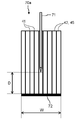
- FIG. 1 is a longitudinal sectional view showing the configuration of the rotating electrical machine according to the first embodiment.
- the rotating electrical machine 100 includes a rotor 10, a stator 20, a frame 6 that surrounds these radially outer sides, and bearing brackets 7 that are provided on both sides of the frame 6 in the axial direction.
- the rotor 10 includes a rotor shaft 11 extending in the longitudinal direction and a rotor core 12 provided on the radially outer side of the rotor shaft 11.
- the rotor shaft 11 is pivotally supported by bearings 5 near both ends.
- Each bearing 5 is fixedly supported by a bearing bracket 7.
- the stator 20 has a stator core 21 disposed with a gap on the outer side in the radial direction of the rotor core 12, and a stator winding 22 penetrating through the stator core 21.
- a plurality of stator slots are formed along the inner surface of the stator core 21 at intervals in the circumferential direction to both ends in the axial direction.
- a conductor 24 for the stator winding 22 (FIG. 2) is disposed in the stator slot.
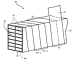
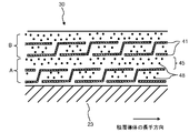
- FIG. 2 is a perspective view for explaining the insulating structure and the tape winding conductor according to the first embodiment.
- a plurality of stator winding conductors 24 constituting the stator winding 22 are laminated and arranged in two rows to form a laminated conductor 23 with 14 bodies.
- the number of stacked layers is 7 and the number of rows is 2 as an example, and the number of layers is not limited to these.
- Each of the stator winding conductors 24 is provided with a turn insulation 25 on the outside thereof and is covered with the turn insulation 25. Therefore, the outer surface of the laminated conductor 23 is also covered with the turn insulation 25.
- the main insulating tape 40 is wound as the main insulation on the outer side of the laminated conductor 23 to which the turn insulation 25 is applied, and the main insulating portion 49 is formed on the outer side of the laminated conductor 23 to form the tape wound conductor 50.
- the width of the main insulating tape 40 is W.
- the main insulating tape 40 is wound in a spiral shape when viewed in the longitudinal direction of the laminated conductor 23.
- the winding method at this time is a half wrap method. That is, the pitch of the helix is, for example, W / 2 that is half the width W of the main insulating tape 40. That is, it is wound so as to overlap with the main insulating tape 40 wound in the previous turn.
- the winding method is not limited to the half wrap method.
- the overlapping width may be changed.
- interval, without overlapping may be sufficient. In this case, the second winding is performed such that, for example, half the width of the main insulating tape 40 is shifted in the longitudinal direction.
- the second winding is further performed from above, and the main insulating tape 40 is layered.
- the winding of the main insulating tape 40 is not limited to twice. For example, it may be three times or more, and may be once, and is selected according to the required insulation performance.
- stator winding conductors 24 is subjected to individual insulation treatment, and mica insulation treatment may be performed from the outside thereof.
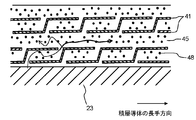
- FIG. 3 is a cross-sectional view schematically showing a configuration of a main insulating tape having an insulating structure according to the first embodiment.
- the main insulating tape 40 constituting the main insulating portion 49 penetrates into the main insulating layer 41, the fiber reinforced portion 42, and the fiber reinforced portion 42, and a nanoparticle-containing joint that joins the fiber reinforced portion 42 and the main insulating layer 41.
- the polymer polymer 43 for use is included.
- the main insulating layer 41 is a part that basically assumes an insulating function.
- the fiber reinforced portion 42 is a portion having a function of securing the strength as the main insulating tape 40 by supporting the main insulating layer 41 along the main insulating layer 41.
- the material of the main insulating layer 41 is, for example, mica, asbestos, or porcelain.
- the material of the fiber reinforcement part 42 is glass fiber etc., for example, and is normally knitted in mesh shape.
- the nanoparticle-containing bonding polymer 43 is, for example, an unsaturated polyester resin or an epoxy resin.
- the thickness of the main insulating layer 41 is, for example, about 100 ⁇ m. Moreover, the thickness of the fiber reinforced part 42 is thinner than this, for example, about 30 micrometers.
- the fiber reinforced portion 42, the nanoparticle-containing bonding polymer polymer 43 and the main insulating layer 41 are illustrated as the constituent parts of the main insulating tape 40. It has the role of joining the main insulating layer 41 and the fiber reinforced portion 42 while immersing in the fiber reinforced portion 42. For this reason, there is almost no thickness of the part only of the polymer polymer 43 for a joint containing a nanoparticle, and the main insulating layer 41 and the fiber reinforcement part 42 are the states which are almost substantially mutually contacting.
- Nanoparticles are kneaded in the polymer polymer 43 for bonding with nanoparticles.
- the nanoparticles for example, silicon dioxide (SiO 2 ), aluminum oxide (Al 2 O 3 ), magnesium oxide (MgO), boron nitride (BN), carbon nanotube (CNT), or the like can be used.
- Nanoparticles are generally said to include particles having a particle size of about several hundred nm.
- the nanoparticles used in the present embodiment are those having a particle size of 100 nm or less, that is, about several tens of nm. When a film having a thickness of about several hundreds of nanometers exceeding 100 nm is used, it is considered that the following effects cannot be expected.
- a manufacturing method of a particle having a particle size of 100 nm or less there is a method of manufacturing by growing from a finer one chemically. Or you may grind
- nanoparticles those having a size of 100 nm or less are referred to as nanoparticles.
- the main insulating tape 40 is wound with the main insulating layer 41 side on the insulating object side and the fiber reinforced portion 42 on the outside.
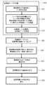
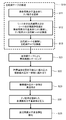
- FIG. 4 is a flowchart showing the procedure of the insulating structure manufacturing method according to the first embodiment.
- the main insulating tape 40 is manufactured (step S10). Specifically, first, nanoparticles are kneaded into the bonding polymer (step S11). That is, nanoparticles are kneaded with the bonding polymer to prepare the bonding polymer 43 with nanoparticles.
- step S12 the sheet-like main insulating layer 41 and the sheet-like fiber reinforced portion 42 are adhered by the polymer polymer 43 for bonding with nanoparticles to produce a main insulating sheet 40a with nanoparticles.
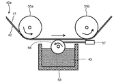
- FIG. 5 is an elevational sectional view showing the state of the main insulating sheet manufacturing step.
- the polymer polymer 43 for bonding with nanoparticles is applied to the sheet-like fiber reinforced portion 42 by using a coating method called a micro gravure method.
- a sheet-like main insulating layer 41 spreading in a plane and a sheet-like fiber reinforced portion 42 spreading along the same are prepared. These are available as raw materials for manufacturing the main insulating tape, that is, as materials for manufacturing the main insulating tape.
- the sheet-like main insulating layer 41 and the sheet-like fiber reinforced portion 42 are overlapped in advance.
- the stacked laminated sheets are continuously driven by a roller 55a and a roller 55b so that the fiber reinforced portion 42 is on the lower side and the main insulating layer 41 is on the upper side.
- the micro gravure roll 56 is in contact with the fiber reinforced portion 42 from below.
- the lower part of the micro gravure roll 56 is immersed in the bonding polymer polymer 43 containing liquid nanoparticles stored in the container 58.
- the micro gravure roll 56 rotates in a direction opposite to the moving direction of the laminated sheet.
- the polymer polymer 43 for bonding with nanoparticles in the container 58 is conveyed upward in a state of adhering to the surface of the microgravure roll 56.
- the excess polymer polymer 43 for bonding containing nanoparticles is removed.
- the polymer polymer 43 for bonding with nanoparticles that has not been removed by the doctor blade 57 contacts the laminated sheet and adheres to the fiber reinforced portion 42 of the laminated sheet.
- the nanoparticle-containing bonding polymer 43 attached to the fiber reinforced portion 42 penetrates into the fiber reinforced portion 42 and reaches the main insulating layer 41. In this way, the polymer polymer 43 for bonding with nanoparticles bonds the main insulating layer 41 and the fiber reinforced portion 42. In this way, the main insulating sheet 40a is manufactured.
- the main insulating sheet 40a is cut to manufacture the main insulating tape 40 (step S13).
- step S21 taping is performed around the laminated conductor 23 with the main insulating tape 40 (step S21). As a result, the tape winding conductor 50 is formed.
- FIG. 6 is a longitudinal sectional view showing the configuration of the integrated winding assembly.
- the integrated winding assembly 90 includes a stator core 21, a stator winding 22, and a frame 6 disposed on the outer side in the radial direction.
- the stator winding 22 is formed by connecting the tape winding conductor 50 (FIG. 2) after being accommodated in a plurality of slots (not shown).
- the slots are formed on the inner surface of the stator core 21 so as to extend to both ends in the axial direction of the stator core 21 at intervals in the circumferential direction.
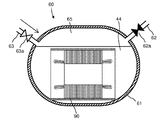
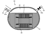
- FIG. 7 is an elevational sectional view showing a state of the vacuuming step.
- the integrated winding assembly 90 is housed in the impregnation container 61 of the impregnation apparatus 60.
- the impregnation container 61 can be divided into upper and lower parts, and the upper and lower parts can be joined with a flange (not shown).
- FIG. 8 is an elevational sectional view showing the state of the press-fitting step of the impregnating polymer. Specifically, after the impregnation vessel 61 is evacuated in step S23, the vacuum exhaust valve 62a on the vacuum exhaust pipe 62 is closed, and the polymer supply valve 63a on the polymer supply pipe 63 is closed. And the impregnating polymer 44 is supplied into the impregnation container. Supply of the polymer polymer for impregnation 44 is performed until the inside of the winding built-in unit 90 is sufficiently immersed in the polymer polymer for impregnation 44.
- the pressurized gas 65 is supplied into the impregnation container 61 from the polymer supply pipe 63, and the impregnation container 61 is supplied. Pressurize the inside.
- the pressurized gas 65 is, for example, an inert gas that is not reactive with the impregnating polymer 44.
- the impregnating polymer 44 penetrates into the main insulating tape 40 applied around the laminated conductor 23, and the main insulating tape 40 impregnates the impregnating polymer 44 into the main insulating tape 40.
- the polymer polymer 44 for use is impregnated to form a polymer polymer portion 45 (FIG. 9).
- the impregnating polymer 44 penetrates into the main insulating tape 40, the polymer polymer 43 for bonding with nanoparticles is reached, the polymer polymer 43 for bonding with nanoparticles is dissolved, and the dissolved nanoparticles are contained.
- the bonding polymer 43 and the impregnation polymer 44 are mixed.
- the nanoparticles in the polymer polymer 43 for bonding with nanoparticles are dispersed around the fiber reinforced portion 42 having the highest concentration, and are dispersed throughout the polymer polymer portion 45 of the main insulating tape 40. spread.
- the polymer polymer 44 for impregnation is solidified (step S25). Specifically, the integrated winding 90 is taken out from the impregnation container 61, and the polymer part 45 (FIG. 9) mainly containing the polymer polymer 42 for impregnation with nanoparticles is solidified.
- the polymer is a thermosetting resin such as an epoxy resin, it is cured by heating or the like.
- the high molecular polymer is a thermoplastic resin, it is cooled and solidified.
- FIG. 9 is a cross-sectional view schematically showing the configuration of the insulating structure according to the first embodiment. The cross section along the longitudinal direction of the laminated conductor 23 which is an insulation object is shown.
- FIG. 9 shows a case where the main insulating tape 40 is wound twice, and the taping layer A by the first winding and the taping layer B by the second winding are formed. Show.
- the insulating structure 30 includes a main insulating layer 41 that is a main insulating portion of the main insulating tape 40 (FIG. 3), a fiber reinforced portion 42 (FIG. 3), and a polymer portion 45.
- the polymer portion 45 is formed by impregnating the polymer polymer 43 for bonding with nanoparticles existing in the fiber reinforced portion 42 and between the fiber reinforced portion 42 and the main insulating layer 41.
- the united body 44 is formed by permeation.
- a polymer part 45 is formed on the outside of the main insulating layer 41 by the impregnating polymer 44 adhering during the impregnation treatment.
- a polymer portion 45 is formed as shown in FIG.
- the thickness of the main insulating layer 41 is displayed extremely thin in order to emphasize the polymer portion 45 formed by entering the fiber reinforced portion 42, and the fiber reinforced portion is also shown.
- the display of the unit 42 is omitted.
- the main insulating layers 41 adjacent to each other in the longitudinal direction of the laminated conductor 23 overlap each other by half of the width. This is a result of winding the main insulating tape 40 described above.
- the nanoparticles 48 contained in the polymer polymer 43 for bonding with nanoparticles are scattered.
- FIG. 10 is a cross-sectional view schematically showing the progress of the electric tree in the conventional insulating structure.
- a curve with a thick arrow schematically shows the path of progress of the electrical tree.
- the high polymer part 45a does not contain nanoparticles.
- the electrical tree emanating from the laminated conductor 23 reaches the surface while passing through the polymer portion 45a between the main insulating layers 41 through a substantially shortest route.
- FIG. 11 is a cross-sectional view schematically showing the effect of the insulating structure according to the first embodiment.
- the insulating structure 30 according to the present embodiment nanoparticles 48 are scattered in the polymer portion 45 between the main insulating layers 41. For this reason, when the nanoparticles 48 are not present, the electric tree advances in the shortest route, and the appearance is changed while changing the direction due to the presence of the nanoparticles 48. As a result, the progress rate is significantly reduced as compared with the case where the nanoparticles 48 are not present. Or the progress stops on the way.
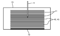
- FIG. 12 is a longitudinal sectional view schematically showing a first test system for an insulating structure according to the first embodiment.
- the first test body 70 simulates a state in which a plurality of mica tapes are stacked. Therefore, the material of the main insulating layer 41 is mica, the fiber reinforced portion 42 is glass fiber, and the material of the high polymer portion 45 is epoxy resin. Epoxy resins do not contain nanoparticles.
- a plurality of main insulating layers 41 are stacked substantially in parallel with each other. Between the main insulating layers 41 adjacent to each other, a fiber reinforced portion 42 and a high polymer portion 45 are disposed.
- the thickness of the main insulating layer 41 was 100 to 140 ⁇ m per layer, and the thickness of the fiber reinforced portion 42 and the polymer portion 45 was 10 to 40 ⁇ m per layer.
- the thickness of the main insulating layer 41 is displayed extremely thin in order to emphasize the polymer portion 45 formed by entering the fiber reinforced portion 42, Moreover, the display of the fiber reinforcement part 42 is abbreviate
- a first test system was set in which the needle electrode 71 was inserted at a substantially central position in the plane of the first test body 70.
- an AC voltage of 50 Hz was applied between the needle electrode 71 and the ground plate 72, and the partial discharge start voltage was measured. After detecting the partial discharge start voltage, the applied voltage was increased at a boosting rate of 600 V / sec until the sample breakdown.
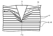
- FIG. 13 is a detailed longitudinal sectional view of a portion around the needle electrode schematically showing a test result of the insulating structure according to the first embodiment.
- the electric tree 75 has advanced in the direction in which the main insulating layer 41 spreads by sewing between the main insulating layers 41 adjacent to each other in the vertical direction, as indicated by broken line arrows in FIG. Further, the electric tree 75 does not originate from the tip portion 71a of the needle electrode 71 having the highest electric field intensity, but from a position slightly off the tip portion 71a (a portion slightly on the side of the tip portion 71a in FIG. 13). The electric tree 75 progresses with a spread in the direction in which the main insulating layer 41 spreads.
- FIG. 14 is a longitudinal sectional view schematically showing a second test system of the insulating structure according to the first embodiment.
- a needle electrode is inserted into the glass cloth portion between the adjacent mica layers, and the polymer polymer portion 45 has no nanoparticles, Each test was performed for the case where it existed.
- the second test body 70 a simulates a state in which a plurality of mica tapes are stacked in the same manner as the first test body 70. Therefore, the material of the main insulating layer 41 is mica, the fiber reinforced portion 42 is glass fiber, and the material of the high polymer portion 45 is epoxy resin.
- the epoxy resin may or may not contain nanoparticles.
- a plurality of main insulating layers 41 are stacked substantially in parallel with each other. Between the main insulating layers 41 adjacent to each other, a fiber reinforced portion 42 and a high polymer portion 45 are disposed.
- a ground plate 72 is provided at an end portion where the main insulating layer 41 and the fiber reinforced portion 42 extend.
- the needle electrode 71 is inserted in the region of the fiber reinforced portion 42 and the polymer portion 45 sandwiched between the main insulating layers 41 adjacent to each other.
- the test was conducted using a system in which the width W of the ground plate was about 4 mm, the depth was about 25 mm, and the distance D between the needle electrode 71 and the ground plate 72 was about 3 mm.
- the time until the dielectric breakdown occurs when the state of 15 kV is maintained was maintained. And compared. In the test results, for example, it was about 1.9 hours when the nanoparticles were not present, whereas it was 3 weeks or more when the nanoparticles were present. In this case, the average particle diameter of the nanoparticles was 10 to 20 nm, and the mixing ratio of the nanoparticles was 10 wt%.
- the thermal conductivity is about 0.25 W / m ⁇ K, for example, 0.40 W / m ⁇ K.
- the thermal conductivity is about 0.25 W / m ⁇ K, for example, 0.40 W / m ⁇ K.
- the heat dissipation effect can be further increased, a current can be further flowed, so that the storage output, that is, the output per unit volume can be increased.
- nanoparticles are mixed in a polymer, depending on the combination, the viscosity of the polymer may increase or the usable life of the polymer may be shortened. In addition, the effect of nanoparticles can be exhibited.
- the progress of the electric tree in the insulating structure can be suppressed, and the storage output can be improved and the efficiency of the assembly work can be improved.
- the polymer polymer with nanoparticles is directly attached, including the case of high concentration where it is difficult to penetrate the nanoparticles, so that nanoparticles of any concentration are applied. It is possible.
- FIG. 15 is a flowchart showing the procedure of the insulating structure manufacturing method according to the second embodiment.
- This embodiment is a modification of the first embodiment.
- the polymer for impregnation kneaded with nanoparticles is press-fitted (step S31).
- step S31 the polymer for impregnation kneaded with nanoparticles
- FIG. 16 is an elevational sectional view showing the state of the press-fitting step of the polymer polymer for impregnation with nanoparticles in the insulating structure manufacturing method according to the second embodiment.
- step S23 in which the inside of the impregnation container 61 of the impregnation apparatus 60 is evacuated, the winding-incorporated integrated article 90 is immersed in the polymer polymer 47 for impregnation with nanoparticles.
- the concentration of the nanoparticles in the polymer polymer 47 for impregnation with nanoparticles may be different from the concentration of the nanoparticles in the polymer polymer 43 for bonding with nanoparticles, depending on the combination of the two concentrations. The optimal nanoparticle concentration distribution can be obtained.
- the inside of the impregnation container 61 is pressurized, and the polymer polymer 47 for impregnation with nanoparticles is press-fitted into the tape winding conductor 50 in the winding built-in integral 90.
- the nanoparticles are included not only in the bonding polymer 43 but also in the impregnation polymer 44, the dispersed state of the nanoparticles can be secured in a wide range. . As a result, the effect of the first embodiment can be further ensured.
Landscapes
- Engineering & Computer Science (AREA)
- Power Engineering (AREA)
- Manufacturing & Machinery (AREA)
- Insulation, Fastening Of Motor, Generator Windings (AREA)
- Manufacture Of Motors, Generators (AREA)
- Inorganic Insulating Materials (AREA)
- Manufacturing Of Electric Cables (AREA)
- Insulating Bodies (AREA)
Abstract
絶縁対象物の外表面を覆う絶縁構造の製造方法は、ナノ粒子が混在した主絶縁シートを製造するシート製造ステップ(S12)と、主絶縁シートを主絶縁テープに裁断する裁断ステップ(S13)と、主絶縁テープにより絶縁対象物の外側にテーピングして絶縁部を形成するテーピングステップ(S21)と、テーピングステップ後に、テーピングされた絶縁対象物を真空引きする真空引きステップ(S23)と、真空引きステップの後に、絶縁部に含浸用高分子重合体を圧入して含浸させる含浸ステップ(S24)とを有する。
Description
本発明は、絶縁構造製造方法、絶縁構造、およびこれを用いた回転電機に関する。
絶縁体に電界が加わり、不平等電界部分が生じ、その部分の電界が絶縁強度限界電圧を超えると、その部分に局部破壊が生ずる。この局部破壊が樹枝状に進展すると電気トリーとなる。電気トリーは、電極と絶縁体との間のエア・ギャップや、異物、絶縁体中の異物・突起物・ボイドなど、高電界集中部が起点となると考えられている。
近年、インバータの利用が進んでいるが、インバータ駆動電動機では、繰り返し、インバータサージを含むインパルス電圧が作用する状態で使用することにより、コイル導線の絶縁材料の寿命が大幅に低下する可能性がある。このため、たとえば、定格電圧3.3kV用のインバータ駆動電動機には、通常の定格電圧6.6kV用の絶縁を使用するような仕様とせざるを得ない等の状況が生じている。
回転電機に使用される導電体の絶縁構造の例として、たとえばコイルの導線は、通常、絶縁材料を有する絶縁体で覆われている。ここで、比較的高温に達する導体については、比較的高温に耐える絶縁階級の高い絶縁材料としてケイ酸塩鉱物の一種であるマイカ(雲母)を用いたマイカ絶縁構造の場合が多い。
電気トリーが進展すれば、マイカ絶縁構造に破壊がもたらされる。マイカ絶縁構造の中において、電気トリーがどのように発生し、進展していくのかを把握することは、電気トリーの発生・進展を防止し、健全な回転電機を維持する上で、きわめて重要な事項である。
このような絶縁材料の健全性については、たとえば、国際電気標準会議(IEC:International Electrotechinical Commission)による、事故防止のための新たな絶縁試験手法を規定した国際規格制定のための動きがある。
たとえば、高圧型巻き電動機において、その絶縁寿命を大きく左右するのは、固定子鉄心の内部に配された主絶縁とターン絶縁である。これらには、いずれもマイカ絶縁構造が多用されている。
また、主絶縁としてのマイカ絶縁構造では、マイカ絶縁テープをエポキシ樹脂で含浸することにより形成される場合が多い。マイカ絶縁テープは、マイカとエポキシガラス層で構成されている。このように構成されたマイカ絶縁テープを、コイル導体に巻回した上で、エポキシ樹脂で含浸することにより、マイカ絶縁構造による絶縁処理がなされる。
このように構成されたマイカ絶縁構造における電気トリーのパスは、マイカ絶縁層を貫通するのではなく、マイカ絶縁層の外側のエポキシガラス層側に形成されることを、試験の結果から確認することができた。すなわち、主絶縁における弱点部分はエポキシガラス層であることが判明した。
本発明は、このような知見に基づいてなされたものであり、絶縁構造における電気トリーの進展を抑制することを目的とする。
上述の目的を達成するため、本発明は、絶縁対象物の外表面を覆う絶縁構造の製造方法であって、ナノ粒子が混在した主絶縁シートを製造するシート製造ステップと、前記主絶縁シートを主絶縁テープに裁断する裁断ステップと、前記主絶縁テープにより前記絶縁対象物の外側にテーピングして主絶縁部を形成したテーピング後絶縁対象物を生成するテーピングステップと、前記テーピングステップの後に前記絶縁対象物を真空引きする真空引きステップと、前記真空引きステップの後に、前記テーピング後絶縁対象に形成された前記絶縁部に、含浸用高分子重合体を圧入して含浸させる含浸ステップと、前記含浸ステップの後に、前記絶縁部を昇温し前記ナノ粒子を含む高分子重合体を固化させる固化ステップと、を有することを特徴とする。
また、本発明は、絶縁対象物の外表面を覆って当該絶縁対象物を電気的に絶縁するために前記絶縁対象物の外表面を覆う絶縁構造であって、前記絶縁対象物の表面に沿って平面的に広がった主絶縁層と、前記主絶縁層に沿って広がった繊維強化部と、前記繊維強化部内に形成されて前記主絶縁層と前記繊維強化部とを互いに接着する高分子重合体部と、を有し、前記高分子重合体部は、前記ナノ粒子が散在し、前記ナノ粒子の濃度は前記繊維強化部において最も高いことを特徴とする。
また、本発明は、軸方向に延びたロータシャフトと、前記ロータシャフトの径方向外側に設けられた回転子鉄心とを有する回転子と、前記回転子鉄心の径方向外側に間隙をあけて設けられた円筒状の固定子鉄心と、前記固定子鉄心の内面に周方向に互いに間隔をあけて形成され前記固定子鉄心の軸方向の両端まで延びる複数のスロット内および前記固定子鉄心の軸方向外側に配された固定子巻線導体と、前記固定子導体を電気的に絶縁するために前記固定子導体に施された絶縁構造と、を有する固定子と、前記ロータシャフトの前記回転子鉄心の軸方向の両側のそれぞれで前記ロータシャフトを回転可能に軸支する2つの軸受と、前記回転子鉄心および前記固定子を収納するフレームと、を備えた回転電機であって、前記絶縁構造は、前記絶縁対象の表面に沿って平面的に広がった主絶縁層と、前記主絶縁層に沿って広がった繊維強化部と、前記繊維強化部内に形成されて前記主絶縁層と前記繊維強化部とを互いに接着する高分子重合体部と、を有し、前記高分子重合体部は、前記ナノ粒子が散在し、前記ナノ粒子の濃度は前記繊維強化部において最も高いことを特徴とする。
本発明によれば、絶縁構造における電気トリーの進展を抑制することができる。
以下、図面を参照して、本発明の実施形態に係る絶縁構造、絶縁構造製造方法およびこれを用いた回転電機について説明する。ここで、互いに同一または類似の部分には、共通の符号を付して、重複説明は省略する。
以下では、回転電機の固定子巻線導体に絶縁構造を適用した場合を例にとって説明するが、絶縁対象物は固定子巻線導体に限定されない。すなわち、導体の外表面を覆う絶縁構造であれば適用可能である。
[第1の実施形態]
図1は、第1の実施形態に係る回転電機の構成を示す縦断面図である。回転電機100は、回転子10、固定子20、これらの径方向外側を囲うフレーム6およびフレーム6の軸方向の両側に設けられた軸受ブラケット7を有する。
図1は、第1の実施形態に係る回転電機の構成を示す縦断面図である。回転電機100は、回転子10、固定子20、これらの径方向外側を囲うフレーム6およびフレーム6の軸方向の両側に設けられた軸受ブラケット7を有する。
回転子10は、長手方向に延びたロータシャフト11と、ロータシャフト11の径方向外側に設けられた回転子鉄心12を有する。ロータシャフト11は、両端付近をそれぞれ軸受5によって回転可能に軸支されている。軸受5は、それぞれ軸受ブラケット7により固定支持されている。
固定子20は、回転子鉄心12の径方向外側に間隙をあけて配された固定子鉄心21と、固定子鉄心21内を貫通する固定子巻線22を有する。
固定子鉄心21の内面に沿って、互いに周方向に間隔をあけて軸方向の両端まで複数の固定子スロット(図示せず)が形成されている。固定子スロット内には、固定子巻線22用の導体24(図2)が配されている。
図2は、第1の実施形態に係る絶縁構造およびテープ巻き導体を説明する斜視図である。
固定子巻線22を構成する複数の固定子巻線導体24は、7体が積層され、それが2列に並んで、14体で積層導体23を形成している。なお、積層数が7体、列数が2列は例であり、これらに限定されず、7体以外、1列あるいは3列以上でもよい。それぞれの固定子巻線導体24には、その外側にターン絶縁25が施され、ターン絶縁25により覆われている。したがって、積層導体23の外面もターン絶縁25により覆われている。
ターン絶縁25が施された積層導体23の外側には、主絶縁として主絶縁テープ40が巻回され、積層導体23の外側に主絶縁部49が形成されて、テープ巻き導体50となる。
ここで、主絶縁テープ40の幅をWとする。主絶縁テープ40は、積層導体23の長手方向に見てらせん状に巻回されている。この際の巻回方式は、ハーフラップ方式である。すなわち、らせんのピッチは、たとえば、主絶縁テープ40の幅Wの半分のW/2である。すなわち、前回のターンで巻かれた主絶縁テープ40と半分重なるようにして巻かれる。なお、巻回方式は、ハーフラップ方式に限らない。たとえば、重ね合わせの幅を変更してもよい。また、重ね合わせることなく、隣接して隙間なく巻回する方式でもよい。この場合は、2回目の巻回は、たとえば、主絶縁テープ40の幅の半分だけ長手方向にずらせるようにして巻回する。
一通り積層導体23の長手方向に巻回されると、さらのその上から2回目の巻回がなされ、主絶縁テープ40は、層状をなす。なお、主絶縁テープ40の巻回は2回に限らない。たとえば、3回以上でもよいし、1回でもよく、必要な絶縁性能により選択される。
なお、固定子巻線導体24のそれぞれには、個別の絶縁処理が施され、その外側から、マイカ絶縁処理を行う場合もある。
図3は、第1の実施形態に係る絶縁構造の主絶縁テープの構成を模式的に示す断面図である。主絶縁部49を構成する主絶縁テープ40は、主絶縁層41、繊維強化部42、および、繊維強化部42に浸透し、繊維強化部42と主絶縁層41とを接合させるナノ粒子入り接合用高分子重合体43を有する。主絶縁層41は、基本的に絶縁機能を担う部分である。また、繊維強化部42は、主絶縁層41に沿って主絶縁層41を支持することにより主絶縁テープ40としての強度を確保する機能を有する部分である。
ここで、主絶縁層41の材質は、たとえば、マイカ、石綿、あるいは磁器などである。また、繊維強化部42の材料は、たとえば、ガラス繊維などであり、通常は、網目状に編み込まれている。また、ナノ粒子入り接合用高分子重合体43は、たとえば、不飽和ポリエステル樹脂、あるいはエポキシ樹脂などである。
主絶縁層41の厚みは、たとえば100μm程度である。また、繊維強化部42の厚みは、これより薄くたとえば30μm程度である。図3において、主絶縁テープ40の構成部分として繊維強化部42、ナノ粒子入り接合用高分子重合体43および主絶縁層41を図示したが、ナノ粒子入り接合用高分子重合体43については、繊維強化部42に浸み込むとともに、主絶縁層41と繊維強化部42を接合する役割を有する。このため、ナノ粒子入り接合用高分子重合体43のみの部分の厚みは殆どなく、主絶縁層41と繊維強化部42は通常は互いに殆ど接している状態である。
ナノ粒子入り接合用高分子重合体43には、ナノ粒子が混練されている。ナノ粒子は、たとえば、二酸化ケイ素(SiO2)、酸化アルミニウム(Al2O3)、酸化マグネシウム(MgO)、窒化ホウ素(BN)、カーボンナノチューブ(CNT)などを用いることができる。
ナノ粒子は、一般的に、粒径が数100nm程度のものまでを含むといわれている。本実施形態で用いるナノ粒子は、100nm以下の粒径のもの、すなわち数十nm程度のものとする。100nmを超えて数百nm程度のものを用いた場合、以下に示すような効果は期待できないと考えられる。
100nm以下の粒径のものの製法としては、化学的に、より微細なものから成長させて製造する方法がある。あるいは、100nmより大きな粒径のものを粉砕して100nm以下のものを製造してもよい。また、ナノ粒子入り接合用高分子重合体43内での凝集を防止するために、表面修飾を行ってもよい。
以下の説明においては、100nm以下のものをナノ粒子と呼ぶこととする。
主絶縁テープ40は、主絶縁層41側を絶縁対象物側、繊維強化部42を外側にして巻回される。
図4は、第1の実施形態に係る絶縁構造製造方法の手順を示すフロー図である。
まず、主絶縁テープ40を製造する(ステップS10)。詳細には、先ず、接合用高分子重合体にナノ粒子を混練する(ステップS11)。すなわち、接合用高分子重合体にナノ粒子を混練して、ナノ粒子入り接合用高分子重合体43を準備する。
次に、シート状の主絶縁層41およびシート状の繊維強化部42をナノ粒子入り接合用高分子重合体43により接着し、ナノ粒子入りの主絶縁シート40aを製造する(ステップS12)。
図5は、主絶縁シートの製造ステップの状態を示す立断面図である。これは、マイクログラビア方式と呼ばれるコーティング方式を用いて、ナノ粒子入り接合用高分子重合体43をシート状の繊維強化部42に塗布するものである。
まず、平面的に広がるシート状の主絶縁層41と、これに沿って広がるシート状の繊維強化部42を準備する。これらは、主絶縁テープ製造用の原反、すなわち主絶縁テープ製造用の素材として入手可能である。
次に、シート状の主絶縁層41とシート状の繊維強化部42とをあらかじめ重ね合わせる。重ね合わせた積層シートを、繊維強化部42が下側、主絶縁層41が上側となるようにして、図5に示すようにローラ55aおよびローラ55bにて連続的に移動駆動する。
この際、マイクログラビアロール56が、繊維強化部42に下側から接している。マイクログラビアロール56は、その下側の部分が、容器58内に貯留された液体状のナノ粒子入り接合用高分子重合体43内に浸漬している。マイクログラビアロール56は、積層シートの移動方向に逆らう方向に回転する。マイクログラビアロール56の回転に伴って、容器58内のナノ粒子入り接合用高分子重合体43がマイクログラビアロール56の表面に付着した状態で上方に搬送される。ここで、ドクターブレード57が、マイクログラビアロール56の表面から所定の間隙を有する位置で、余分のナノ粒子入り接合用高分子重合体43を除去する。
ドクターブレード57により除去されなかったナノ粒子入り接合用高分子重合体43は、積層シートに接し、積層シートの繊維強化部42に付着する。繊維強化部42に付着したナノ粒子入り接合用高分子重合体43は繊維強化部42内に浸透し、主絶縁層41に到達する。このようにして、ナノ粒子入り接合用高分子重合体43は、主絶縁層41と繊維強化部42とを接合する。このようにして、主絶縁シート40aが製造される。
次に、主絶縁シート40aを裁断し、主絶縁テープ40を製造する(ステップS13)。
次に、主絶縁テープ40により、積層導体23の周囲にテーピングを施す(ステップS21)。この結果、テープ巻き導体50が形成される。
次に、積層導体23を固定子鉄心21に組み込み、巻線組み込み一体物に組み立てる(ステップS22)。図6は、巻線組み込み一体物の構成を示す縦断面図である。巻線組み込み一体物90は、固定子鉄心21、固定子巻線22およびこれらの径方向外側に配されたフレーム6を有する。
固定子巻線22は、テープ巻き導体50(図2)を、複数のスロット(図示せず)内に収納した上で結線することにより形成される。スロットは、固定子鉄心21の内側表面に周方向に間隔をもって固定子鉄心21の軸方向の両端まで延びるように形成される。
次に、巻線組み込み一体物90の真空引きを行う(ステップS23)。図7は、真空引きステップの状態を示す立断面図である。具体的には、まず、巻線組み込み一体物90を、含浸装置60の含浸用容器61内に収納する。なお、巻線組み込み一体物90の出し入れは、たとえば、含浸用容器61が上下に分割可能で図示しないフランジで上下を結合させるような構成とする。
高分子重合体供給配管63上の高分子重合体供給弁63aおよび真空排気配管62上の真空排気弁62aを閉じて、含浸用容器61を密閉状態とした後に、たとえば、真空ポンプ(図示せず)に接続された真空排気配管62上の真空排気弁62aを開き、含浸用容器61内を真空引きする。この結果、含浸用容器61内に収納された巻線組み込み一体物90内のテープ巻き導体50の主絶縁テープ40内の各空間部も真空引きされる。
次に、含浸用高分子重合体44を圧入する(含浸ステップS24)。図8は、含浸用高分子重合体の圧入ステップの状態を示す立断面図である。具体的には、ステップS23で含浸用容器61内が真空引きされた後に、真空排気配管62上の真空排気弁62aを閉じて、高分子重合体供給配管63上の高分子重合体供給弁63aを開き、含浸用高分子重合体44を含浸用容器内に供給する。含浸用高分子重合体44の供給は、巻線組み込み一体物90内が含浸用高分子重合体44に十分に浸漬するまで行う。
巻線組み込み一体物90が含浸用高分子重合体44に十分に浸漬する状態となったら、高分子重合体供給配管63から加圧ガス65を含浸用容器61内に供給し、含浸用容器61内を加圧する。ここで、加圧ガス65は、含浸用高分子重合体44と反応性のないたとえば不活性ガスなどを用いる。
この結果、含浸用高分子重合体44が、積層導体23の周囲に施された主絶縁テープ40内に浸透し、主絶縁テープ40が含浸用高分子重合体44を含浸主絶縁テープ40が含浸用高分子重合体44を含浸し、高分子重合体部45(図9)を形成する状態となる。含浸用高分子重合体44が、主絶縁テープ40内に浸透すると、ナノ粒子入り接合用高分子重合体43に至り、ナノ粒子入り接合用高分子重合体43が溶解し、溶解したナノ粒子入り接合用高分子重合体43と含浸用高分子重合体44が混合する。この結果、ナノ粒子入り接合用高分子重合体43内のナノ粒子は、最も濃度の高い繊維強化部42を中心に、分散して、主絶縁テープ40の高分子重合体部45内の全体に広がる。
次に、含浸用高分子重合体44の固化を行う(ステップS25)。具体的には、巻線組み込み一体物90を含浸用容器61から取り出し、ナノ粒子入り含浸用高分子重合体42を主に含む高分子重合体部45(図9)を固化させる。なお、高分子重合体がエポキシ樹脂などの熱硬化性樹脂の場合は、加熱等により硬化させる。また、高分子重合体が熱可塑性樹脂の場合は冷却し固化させる。
図9は、第1の実施形態に係る絶縁構造の構成を模式的に示す断面図である。絶縁対象物である積層導体23の長手方向に沿った断面を示している。図9は、主絶縁テープ40の巻回が2回なされ、第1回目の巻回によるテーピング層Aと、第2回目の巻回によるテーピング層Bと、2つの層が形成されている場合を示す。
絶縁構造30は、主絶縁テープ40(図3)の主絶縁部分である主絶縁層41と、繊維強化部42(図3)と、高分子重合体部45を有する。ここで、高分子重合体部45は、繊維強化部42内および繊維強化部42と主絶縁層41との間に存在していたナノ粒子入り接合用高分子重合体43に含浸用高分子重合体44が浸透して形成されたものである。また、主絶縁層41の外側にも、含浸処理の際に付着した含浸用高分子重合体44により、高分子重合体部45が形成されており、繊維強化部42の内部のみならず、主絶縁層41の周囲には、図9に示すように高分子重合体部45が形成されている。
なお、図9ないし図13においては、繊維強化部42に入り込んで形成された高分子重合体部45を強調するために、主絶縁層41の厚さを極端に薄く表示し、また、繊維強化部42の表示を省略している。
テーピング層Aおよびテーピング層Bのそれぞれにおいては、積層導体23の長手方向に互いに隣接する主絶縁層41同士は、幅の半分ずつ、互いに重なり合っている。これは、前述した主絶縁テープ40の巻き方による結果である。
主絶縁層41の周囲の高分子重合体部45には、ナノ粒子入り接合用高分子重合体43に含まれていたナノ粒子48が散在した状態となっている。
図10は、従来方式の絶縁構造における電気トリーの進展を模式的に示す断面図である。太い矢印付の曲線は、電気トリーの進展パスを模式的に示したものである。高分子重合体部45aはナノ粒子を含んでいない。積層導体23から発した電気トリーは、主絶縁層41の間の高分子重合体部45aをほぼ最短ルートで抜けながら、表面に到達する。
図11は、第1の実施形態に係る絶縁構造の効果を模式的に示す断面図である。本実施形態による絶縁構造30においては、主絶縁層41間の高分子重合体部45にナノ粒子48が散在している。このため、ナノ粒子48が無い場合に電気トリーが最短ルートで進展するのとは様相が異なり、ナノ粒子48の存在によって方向を変えながら進展する。この結果、ナノ粒子48が無い場合に比べて進展速度が大幅に低下する。あるいは、途中でその進展が停止する。
ナノ粒子の存在下での電気トリーの進展の様子を確認する試験を行った。以下にこの試験の結果を説明する。
図12は、第1の実施形態に係る絶縁構造の第1の試験体系を模式的に示す縦断面図である。第1の試験体70は、複数のマイカテープを積層した状態を模擬している。したがって、主絶縁層41の材質はマイカ、繊維強化部42はガラス繊維、高分子重合体部45の材質はエポキシ樹脂である。エポキシ樹脂は、ナノ粒子を含まない。
複数の主絶縁層41が互いにほぼ平行に積層されている。互いに隣接する主絶縁層41の間には、繊維強化部42と高分子重合体部45が配されている。
主絶縁層41の厚みは、1層当たり100~140μmであり、繊維強化部42と高分子重合体部45の層の厚みは、1層当たり10~40μmであった。但し、図12および図13では、前述のように、繊維強化部42に入り込んで形成された高分子重合体部45を強調するために、主絶縁層41の厚さを極端に薄く表示し、また、繊維強化部42の表示を省略している。
第1の試験体70の平面的にほぼ中央の位置に針電極71を差し込んだ第1の試験体系を設定した。この体系で、針電極71と接地板72との間に50Hzの交流電圧を印加し、部分放電開始電圧を測定した。部分放電開始電圧を検出した後に、サンプルが絶縁破壊するまで、600V/secの昇圧速度で印加電圧を上昇させた。
図13は、第1の実施形態に係る絶縁構造の試験結果を模式的に示す針電極周辺の部分の詳細縦断面図である。試験の結果、電気トリー75は、図13に破線矢印で示すように、上下に互いに隣接する主絶縁層41の間を縫って主絶縁層41の広がる方向に進展している。また、電気トリー75は、電界強度の最も高い針電極71の先端部分71aではなく、先端部分71aを少し外れた位置(図13の先端部分71aより少し根本側の部分)から発している。電気トリー75は、主絶縁層41の広がる方向に、広がりをもって進展している。
以上の第1の試験体70を用いた第1の試験体系での試験の結果、互いに隣接した主絶縁層41の間の繊維強化部42中の樹脂部分が弱いということが確認できた。
図14は、第1の実施形態に係る絶縁構造の第2の試験体系を模式的に示す縦断面図である。第1の試験体系での試験結果を受けて、互いに隣接したマイカ層の間のガラスクロス部に針電極を挿入して、高分子重合体部45にナノ粒子が存在しない場合と、ナノ粒子が存在する場合について、それぞれ試験を行った。
第2の試験体70aは、第1の試験体70と同様に複数のマイカテープを積層した状態を模擬している。したがって、主絶縁層41の材質はマイカ、繊維強化部42はガラス繊維、高分子重合体部45の材質はエポキシ樹脂である。エポキシ樹脂は、ナノ粒子を含む場合と、含まない場合とがある。
複数の主絶縁層41が互いにほぼ平行に積層されている。互いに隣接する主絶縁層41の間には、繊維強化部42と高分子重合体部45が配されている。主絶縁層41および繊維強化部42が延びた端部に接地板72が設けられている。針電極71は、互いに隣接する主絶縁層41に挟まれた繊維強化部42と高分子重合体部45の領域に挿入されている。接地板の幅Wは約4mm、奥行きは約25mm、針電極71と接地板72との間隔Dは約3mmの体系で試験を行った。
試験は、電圧を、1kVから1kVずつ15kVまで上昇した後に、15kVの状態を保った場合の絶縁破壊に至るまでの時間を、高分子重合体部45にナノ粒子が存在しない場合と存在する場合とを比較した。試験結果では、たとえば、ナノ粒子が存在しない場合は約1.9時間であったのに対して、ナノ粒子が存在する場合は3週間以上であった。この場合、ナノ粒子の平均粒径は10ないし20nm、ナノ粒子の混在率は10wt%であった。
以上のように、高分子重合体部45にナノ粒子を混在させた場合は、電気的な絶縁寿命が大幅に増加する。
また、ナノ粒子を混在させた場合は、熱伝導率が上昇すること、および機械的強度が高くなることが知られている。
たとえば、熱伝導率は、高分子重合体部45にナノ粒子が混在していない場合には、たとえば、0.25W/m・K程度であったものが、たとえば、0.40W/m・K程度まで上昇する。この結果、放熱効果をより大きくできることから電流をより流すことができるため、収納出力、すなわち単位体積当たりの出力を高めることができる。
また、機械的強度が高くなることにより、従来は巻線の固定作業に仮の補強等を要していたものが簡素化され、組立作業の効率化を図ることができる。更にまた、高分子重合体にナノ粒子を混合した場合、その組み合わせによっては高分子重合体の粘度が上昇したり、あるいは高分子重合体の可使寿命が短くなる場合があるが、これらを排除しながらかつナノ粒子の効果を発揮させることが可能である。
以上のように、本実施形態によれば、絶縁構造における電気トリーの進展を抑制することができ、さらに収納出力の向上、組立作業の効率化を図ることができる。また、たとえば、含浸の場合だとナノ粒子を浸透させることが難しい高濃度の場合を含めて、ナノ粒子入り高分子重合体を直接付着させる方式であるため、任意の濃度のナノ粒子を付与することが可能である。
[第2の実施形態]
図15は、第2の実施形態に係る絶縁構造製造方法の手順を示すフロー図である。本実施形態は、第1の実施形態の変形である。本実施形態で、第1の実施形態における含浸用高分子重合体を圧入するステップS24に代えて、ナノ粒子を混練した含浸用高分子重合体を圧入する(ステップS31)。
その他については、第1の実施形態と同様である。
図15は、第2の実施形態に係る絶縁構造製造方法の手順を示すフロー図である。本実施形態は、第1の実施形態の変形である。本実施形態で、第1の実施形態における含浸用高分子重合体を圧入するステップS24に代えて、ナノ粒子を混練した含浸用高分子重合体を圧入する(ステップS31)。
その他については、第1の実施形態と同様である。
図16は、第2の実施形態に係る絶縁構造製造方法におけるナノ粒子入り含浸用高分子重合体の圧入ステップの状態を示す立断面図である。含浸装置60の含浸用容器61内を真空にしたステップS23の後に、ナノ粒子入り含浸用高分子重合体47に巻線組み込み一体物90を浸漬させる。この場合、ナノ粒子入り含浸用高分子重合体47中のナノ粒子の濃度は、ナノ粒子入り接合用高分子重合体43中のナノ粒子の濃度とは異なる濃度でよく、両者の濃度の組合せにより、最適のナノ粒子の濃度分布を得ることができる。
この後に、含浸用容器61内を加圧し、ナノ粒子入り含浸用高分子重合体47を巻線組み込み一体物90内のテープ巻き導体50に圧入する。
このようにすることにより、ナノ粒子が、接合用高分子重合体43のみでなく、含浸用高分子重合体44にも含まれるため、広い範囲で、ナノ粒子の散在状態を確保することができる。この結果、第1の実施形態の効果をさらに確実にすることができる。
[その他の実施形態]
以上、本発明の実施形態を説明したが、実施形態は例として提示したものであり、発明の範囲を限定することは意図していない。たとえば、実施形態では、主絶縁の巻回がハーフラップ方式の場合を示したが、これに限定されない。たとえば、長手方向に主絶縁テープの端部同士が隣接するような巻回方式であってもよい。
以上、本発明の実施形態を説明したが、実施形態は例として提示したものであり、発明の範囲を限定することは意図していない。たとえば、実施形態では、主絶縁の巻回がハーフラップ方式の場合を示したが、これに限定されない。たとえば、長手方向に主絶縁テープの端部同士が隣接するような巻回方式であってもよい。
さらに、実施形態は、その他の様々な形態で実施されることが可能であり、発明の要旨を逸脱しない範囲で、種々の省略、置き換え、変更を行うことができる。
実施形態やその変形は、発明の範囲や要旨に含まれると同様に、特許請求の範囲に記載された発明とその均等の範囲に含まれるものである。
5…軸受、6…フレーム、7…軸受ブラケット、10…回転子、11…ロータシャフト、12…回転子鉄心、20…固定子、21…固定子鉄心、22…固定子巻線、23…積層導体、24…固定子巻線導体、25…ターン絶縁、30…絶縁構造、40…主絶縁テープ、40a…主絶縁シート、41…主絶縁層、42…繊維強化部、43…ナノ粒子入り接合用高分子重合体、44…含浸用高分子重合体、45、45a…高分子重合体部、47…ナノ粒子入り含浸用高分子重合体、48…ナノ粒子、49…主絶縁部、50…テープ巻き導体、55a、55b…ローラ、56…マイクログラビアロール、57…ドクターブレード、58…容器、60…含浸装置、61…含浸用容器、62…真空排気配管、62a…真空排気弁、63…高分子重合体供給配管、63a…高分子重合体供給弁、65…加圧ガス、70…第1の試験体、70a…第2の試験体、71…針電極、71a…先端部分、72…接地板、75…電気トリー、90…巻線組み込み一体物、100…回転電機、
Claims (10)
- 絶縁対象物の外表面を覆う絶縁構造の製造方法であって、
ナノ粒子が混在した主絶縁シートを製造するシート製造ステップと、
前記主絶縁シートを主絶縁テープに裁断する裁断ステップと、
前記主絶縁テープにより前記絶縁対象物の外側にテーピングして主絶縁部を形成したテーピング後絶縁対象物を生成するテーピングステップと、
前記テーピングステップの後に前記絶縁対象物を真空引きする真空引きステップと、
前記真空引きステップの後に、前記テーピング後絶縁対象に形成された前記絶縁部に、含浸用高分子重合体を圧入して含浸させる含浸ステップと、
前記含浸ステップの後に、前記絶縁部を昇温し前記ナノ粒子を含む高分子重合体を固化させる固化ステップと、
を有することを特徴とする絶縁構造製造方法。 - 前記絶縁対象物は回転電機の固定子巻線の積層導体であって、
前記テーピングステップの後であって、前記真空引きステップの前に、前記テーピングされた積層導体を固定子に組み込み、巻線組み込み一体物に組み立てる組み立てステップをさらに有し、
前記真空引きステップは、前記巻線組み込み一体物を真空引きすることにより、前記テーピングされた前記絶縁対象物を真空引きする、
ことを特徴とする請求項1に記載の絶縁構造製造方法。 - 前記テーピングステップは、前記主絶縁テープの幅の半分ずつずらすハーフラップ方式により前記主絶縁テープを巻回することを特徴とする請求項1または請求項2に記載の絶縁構造製造方法。
- 前記シート製造ステップは、
接着用高分子重合体にナノ粒子を混練してナノ粒子入り接合用高分子重合体を製造する接合用高分子重合体製造ステップと、
平面状に拡がる主絶縁層および前記主絶縁層に沿って平面状に広がる繊維強化部を前記ナノ粒子入り接合用高分子重合体により接合させることによりナノ粒子入りの主絶縁シートを製造する接合ステップと、
を有することを特徴とする請求項1ないし請求項3のいずれか一項に記載の絶縁構造製造方法。 - 前記接合ステップは、マイクログラビア方式による前記ナノ粒子入り接着用高分子重合体の塗布ステップを有することを特徴とする請求項4に記載の絶縁構造製造方法。
- 前記含浸ステップで圧入する含浸用高分子重合体にはナノ粒子が混練されていることを特徴とする請求項1または請求項5に記載の絶縁構造製造方法。
- 前記ナノ粒子は、二酸化ケイ素、酸化アルミニウム、酸化マグネシウム、窒化ホウ素およびカーボンナノチューブの少なくとも一つを用いることを特徴とする請求項1ないし請求項6のいずれか一項に記載の絶縁構造製造方法。
- 前記主絶縁テープは、マイカおよびガラス繊維の少なくとも一方を含むことを特徴とする請求項1ないし請求項7のいずれか一項に記載の絶縁構造製造方法。
- 絶縁対象物の外表面を覆って当該絶縁対象物を電気的に絶縁するために前記絶縁対象物の外表面を覆う絶縁構造であって、
前記絶縁対象物の表面に沿って平面的に広がった主絶縁層と、
前記主絶縁層に沿って広がった繊維強化部と、
前記繊維強化部内に形成されて前記主絶縁層と前記繊維強化部とを互いに接着する高分子重合体部と、
を有し、
前記高分子重合体部は、前記ナノ粒子が散在し、前記ナノ粒子の濃度は前記繊維強化部において最も高いことを特徴とする絶縁構造。 - 軸方向に延びたロータシャフトと、前記ロータシャフトの径方向外側に設けられた回転子鉄心とを有する回転子と、
前記回転子鉄心の径方向外側に間隙をあけて設けられた円筒状の固定子鉄心と、前記固定子鉄心の内面に周方向に互いに間隔をあけて形成され前記固定子鉄心の軸方向の両端まで延びる複数のスロット内および前記固定子鉄心の軸方向外側に配された固定子巻線導体と、前記固定子導体を電気的に絶縁するために前記固定子導体に施された絶縁構造と、を有する固定子と、
前記ロータシャフトの前記回転子鉄心の軸方向の両側のそれぞれで前記ロータシャフトを回転可能に軸支する2つの軸受と、
前記回転子鉄心および前記固定子を収納するフレームと、
を備えた回転電機であって、
前記絶縁構造は、
前記絶縁対象の表面に沿って平面的に広がった主絶縁層と、
前記主絶縁層に沿って広がった繊維強化部と、
前記繊維強化部内に形成されて前記主絶縁層と前記繊維強化部とを互いに接着する高分子重合体部と、
を有し、
前記高分子重合体部は、前記ナノ粒子が散在し、前記ナノ粒子の濃度は前記繊維強化部において最も高いことを特徴とする回転電機。
Priority Applications (5)
| Application Number | Priority Date | Filing Date | Title |
|---|---|---|---|
| JP2018524585A JP6816141B2 (ja) | 2016-07-01 | 2016-07-01 | 絶縁構造製造方法 |
| PCT/JP2016/003164 WO2018002972A1 (ja) | 2016-07-01 | 2016-07-01 | 絶縁構造製造方法、絶縁構造および回転電機 |
| EP16907207.1A EP3480921B1 (en) | 2016-07-01 | 2016-07-01 | Method for producing insulating structure |
| CN201680084475.0A CN109075643A (zh) | 2016-07-01 | 2016-07-01 | 绝缘结构制造方法、绝缘结构及旋转电机 |
| US16/227,933 US10931159B2 (en) | 2016-07-01 | 2018-12-20 | Electrical insulating structure producing method, electrical insulating structure and rotating electrical machine |
Applications Claiming Priority (1)
| Application Number | Priority Date | Filing Date | Title |
|---|---|---|---|
| PCT/JP2016/003164 WO2018002972A1 (ja) | 2016-07-01 | 2016-07-01 | 絶縁構造製造方法、絶縁構造および回転電機 |
Related Child Applications (1)
| Application Number | Title | Priority Date | Filing Date |
|---|---|---|---|
| US16/227,933 Continuation US10931159B2 (en) | 2016-07-01 | 2018-12-20 | Electrical insulating structure producing method, electrical insulating structure and rotating electrical machine |
Publications (1)
| Publication Number | Publication Date |
|---|---|
| WO2018002972A1 true WO2018002972A1 (ja) | 2018-01-04 |
Family
ID=60785373
Family Applications (1)
| Application Number | Title | Priority Date | Filing Date |
|---|---|---|---|
| PCT/JP2016/003164 WO2018002972A1 (ja) | 2016-07-01 | 2016-07-01 | 絶縁構造製造方法、絶縁構造および回転電機 |
Country Status (5)
| Country | Link |
|---|---|
| US (1) | US10931159B2 (ja) |
| EP (1) | EP3480921B1 (ja) |
| JP (1) | JP6816141B2 (ja) |
| CN (1) | CN109075643A (ja) |
| WO (1) | WO2018002972A1 (ja) |
Cited By (2)
| Publication number | Priority date | Publication date | Assignee | Title |
|---|---|---|---|---|
| WO2020144859A1 (ja) * | 2019-01-11 | 2020-07-16 | 東芝三菱電機産業システム株式会社 | 絶縁構造製造方法、絶縁構造製造装置、および回転電機 |
| WO2023132102A1 (ja) * | 2022-01-07 | 2023-07-13 | 日立Astemo株式会社 | 回転電機の固定子 |
Families Citing this family (2)
| Publication number | Priority date | Publication date | Assignee | Title |
|---|---|---|---|---|
| CN110707886B (zh) * | 2019-12-03 | 2021-04-20 | 哈尔滨电机厂有限责任公司 | 一种大型电机转子磁极极身绝缘贴附式粘接的工艺方法 |
| CN113506662B (zh) * | 2021-07-08 | 2022-07-12 | 萍乡强盛电瓷制造有限公司 | 一种盘形悬式瓷绝缘子加工用设备 |
Citations (4)
| Publication number | Priority date | Publication date | Assignee | Title |
|---|---|---|---|---|
| JPS63110929A (ja) * | 1986-10-22 | 1988-05-16 | アセア アクチーボラグ | 電気機器の固定子又は回転子におけるスロツト内に配置するためのコイル |
| JPH10174333A (ja) * | 1996-12-10 | 1998-06-26 | Fuji Electric Co Ltd | 回転機固定子コイル |
| WO2015053374A1 (ja) * | 2013-10-09 | 2015-04-16 | 日立化成株式会社 | プリプレグマイカテープ及びそれを用いたコイル |
| WO2016104141A1 (ja) * | 2014-12-22 | 2016-06-30 | 三菱電機株式会社 | 絶縁テープ及びその製造方法、並びに固定子コイル及びその製造方法、並びに発電機 |
Family Cites Families (15)
| Publication number | Priority date | Publication date | Assignee | Title |
|---|---|---|---|---|
| US2808981A (en) * | 1954-06-09 | 1957-10-08 | Nat Radiator Company | Universal foot for blower assembly |
| GB1352733A (en) * | 1971-07-08 | 1974-05-08 | Mullard Ltd | Electron multipliers |
| JPS5060705A (ja) * | 1973-10-01 | 1975-05-24 | ||
| KR960007166A (ko) * | 1994-08-10 | 1996-03-22 | 김은영 | 골판지 포장 충전재 제조방법과, 이를 수행하기 위한 골판지 권취 및 접착장치, 및 골판지 충전재 성형장치 |
| KR100359109B1 (ko) * | 2000-02-25 | 2002-11-04 | 삼성전자 주식회사 | 시트 코팅 장치 |
| CN1324615C (zh) * | 2002-07-04 | 2007-07-04 | 株式会社东芝 | 高导热性绝缘部件及其制造方法、电磁线圈 |
| US7524557B2 (en) * | 2002-07-04 | 2009-04-28 | Kabushiki Kaisha Toshiba | Highly heat conductive insulating member, method of manufacturing the same and electromagnetic device |
| JP4313141B2 (ja) * | 2003-09-30 | 2009-08-12 | 中川特殊鋼株式会社 | 磁性基材の積層体の製造方法、およびこれにより得られる磁性基材の積層体 |
| JP2006246599A (ja) * | 2005-03-02 | 2006-09-14 | Toshiba Corp | 半導電性テープ、半導電性テープの製造方法、絶縁コイル及び回転電機 |
| CN100506530C (zh) * | 2006-06-12 | 2009-07-01 | 苏州市好护理医疗用品有限公司 | 一种粘性弹性绷带的制作方法 |
| DE102011083409A1 (de) | 2011-09-26 | 2013-03-28 | Siemens Aktiengesellschaft | Isoliersysteme mit verbesserter Teilentladungsbeständigkeit, Verfahren zur Herstellung dazu |
| CN102510141B (zh) * | 2011-10-31 | 2014-01-29 | 安泰科技股份有限公司 | 轴向磁通电机用非晶、微晶或纳米晶合金定子铁心及其制造方法 |
| US9928935B2 (en) * | 2013-05-31 | 2018-03-27 | General Electric Company | Electrical insulation system |
| CN103400638B (zh) * | 2013-07-30 | 2016-01-20 | 苏州巨峰电气绝缘系统股份有限公司 | 一种耐电晕槽绝缘材料及其制备方法 |
| CN204746771U (zh) * | 2015-06-30 | 2015-11-11 | 浙江索凡胶粘制品有限公司 | 一种能够自动上胶自动调节压辊高度的涂布机上胶装置 |
-
2016
- 2016-07-01 EP EP16907207.1A patent/EP3480921B1/en active Active
- 2016-07-01 CN CN201680084475.0A patent/CN109075643A/zh active Pending
- 2016-07-01 JP JP2018524585A patent/JP6816141B2/ja active Active
- 2016-07-01 WO PCT/JP2016/003164 patent/WO2018002972A1/ja unknown
-
2018
- 2018-12-20 US US16/227,933 patent/US10931159B2/en active Active
Patent Citations (4)
| Publication number | Priority date | Publication date | Assignee | Title |
|---|---|---|---|---|
| JPS63110929A (ja) * | 1986-10-22 | 1988-05-16 | アセア アクチーボラグ | 電気機器の固定子又は回転子におけるスロツト内に配置するためのコイル |
| JPH10174333A (ja) * | 1996-12-10 | 1998-06-26 | Fuji Electric Co Ltd | 回転機固定子コイル |
| WO2015053374A1 (ja) * | 2013-10-09 | 2015-04-16 | 日立化成株式会社 | プリプレグマイカテープ及びそれを用いたコイル |
| WO2016104141A1 (ja) * | 2014-12-22 | 2016-06-30 | 三菱電機株式会社 | 絶縁テープ及びその製造方法、並びに固定子コイル及びその製造方法、並びに発電機 |
Cited By (2)
| Publication number | Priority date | Publication date | Assignee | Title |
|---|---|---|---|---|
| WO2020144859A1 (ja) * | 2019-01-11 | 2020-07-16 | 東芝三菱電機産業システム株式会社 | 絶縁構造製造方法、絶縁構造製造装置、および回転電機 |
| WO2023132102A1 (ja) * | 2022-01-07 | 2023-07-13 | 日立Astemo株式会社 | 回転電機の固定子 |
Also Published As
| Publication number | Publication date |
|---|---|
| US20190149009A1 (en) | 2019-05-16 |
| CN109075643A (zh) | 2018-12-21 |
| EP3480921A1 (en) | 2019-05-08 |
| US10931159B2 (en) | 2021-02-23 |
| EP3480921B1 (en) | 2022-06-22 |
| JP6816141B2 (ja) | 2021-01-20 |
| EP3480921A4 (en) | 2020-03-04 |
| JPWO2018002972A1 (ja) | 2019-06-13 |
Similar Documents
| Publication | Publication Date | Title |
|---|---|---|
| WO2018002970A1 (ja) | 絶縁構造製造方法、絶縁構造および回転電機 | |
| WO2018002972A1 (ja) | 絶縁構造製造方法、絶縁構造および回転電機 | |
| JP4913551B2 (ja) | 回転電機巻線及び回転電機並びにそれに用いる半導電性絶縁基材 | |
| JP4103390B2 (ja) | 絶縁材及び電機巻線とその製造法 | |
| WO2018002971A1 (ja) | 絶縁構造製造方法、絶縁構造および回転電機 | |
| US10903710B2 (en) | Producing method for electrical insulating structure, electrical insulating structure and rotating electrical machine | |
| JP2016072301A (ja) | 絶縁材、この絶縁材を用いた絶縁コイル、これらの製造方法、ならびにこの絶縁コイルを具備する装置 | |
| WO2018002974A1 (ja) | コロナ放電防止構造製造方法、コロナ放電防止構造および回転電機 | |
| WO2020144859A1 (ja) | 絶縁構造製造方法、絶縁構造製造装置、および回転電機 | |
| US20220356311A1 (en) | Method of producing resin and method of producing insulating structure | |
| WO2023170794A1 (ja) | 回転電機及び絶縁テープ |
Legal Events
| Date | Code | Title | Description |
|---|---|---|---|
| 121 | Ep: the epo has been informed by wipo that ep was designated in this application |
Ref document number: 16907207 Country of ref document: EP Kind code of ref document: A1 |
|
| ENP | Entry into the national phase |
Ref document number: 2018524585 Country of ref document: JP Kind code of ref document: A |
|
| NENP | Non-entry into the national phase |
Ref country code: DE |
|
| ENP | Entry into the national phase |
Ref document number: 2016907207 Country of ref document: EP Effective date: 20190201 |