WO2017221607A1 - 蛍光体層付光半導体素子 - Google Patents
蛍光体層付光半導体素子 Download PDFInfo
- Publication number
- WO2017221607A1 WO2017221607A1 PCT/JP2017/019060 JP2017019060W WO2017221607A1 WO 2017221607 A1 WO2017221607 A1 WO 2017221607A1 JP 2017019060 W JP2017019060 W JP 2017019060W WO 2017221607 A1 WO2017221607 A1 WO 2017221607A1
- Authority
- WO
- WIPO (PCT)
- Prior art keywords
- white
- optical semiconductor
- phosphor
- layer
- phosphor layer
- Prior art date
Links
Images


Classifications
-
- H—ELECTRICITY
- H01—ELECTRIC ELEMENTS
- H01L—SEMICONDUCTOR DEVICES NOT COVERED BY CLASS H10
- H01L33/00—Semiconductor devices with at least one potential-jump barrier or surface barrier specially adapted for light emission; Processes or apparatus specially adapted for the manufacture or treatment thereof or of parts thereof; Details thereof
- H01L33/48—Semiconductor devices with at least one potential-jump barrier or surface barrier specially adapted for light emission; Processes or apparatus specially adapted for the manufacture or treatment thereof or of parts thereof; Details thereof characterised by the semiconductor body packages
Definitions
- the present invention relates to an optical semiconductor element with a phosphor layer.
- a light-emitting device such as a white light-emitting device that includes a light-emitting diode element and a phosphor layer and emits white light is known (for example, see Patent Document 1).
- the light emitting device of Patent Document 1 includes a diode substrate, a light emitting diode element flip-chip mounted on the diode substrate, a phosphor layer in direct contact with the upper surface of the light emitting diode element, and a side surface of the light emitting diode element. And a reflective resin layer in direct contact.
- An object of the present invention is to provide a phosphor layer-attached optical semiconductor element having excellent junction reliability and heat dissipation while maintaining good brightness.
- the present invention [1] includes an optical semiconductor element having a light emitting surface and an opposing surface disposed to be opposed to the light emitting surface at an interval in a vertical direction, a white film disposed on the upper side of the light emitting surface, A phosphor layer disposed on the upper side of the white film, wherein the white film has a thickness of 2 ⁇ m or more and 15 ⁇ m or less.
- the present invention [2] includes the optical semiconductor element with a phosphor layer according to [1], wherein the white film has a thickness of 2 ⁇ m or more and 7 ⁇ m or less.
- the present invention [3] includes the optical semiconductor element with a phosphor layer according to [1] or [2], further comprising a white portion arranged around the optical semiconductor element.
- the white film includes the optical semiconductor element with a phosphor layer according to any one of [1] to [3] containing white particles.
- the present invention [5] includes the optical semiconductor element with a phosphor layer according to [4], wherein the white particles have an average particle diameter of 0.1 ⁇ m or more and 2.0 ⁇ m or less.
- the phosphor layer-coated optical semiconductor element of the present invention has excellent bonding reliability and heat dissipation while maintaining good brightness.
- FIG. 1A to 1B show a first embodiment of an optical semiconductor device with a phosphor layer according to the present invention.
- FIG. 1A is a plan view
- FIG. 1B is a cross-sectional view taken along line AA of FIG. 1A.
- 2A to 2G are process diagrams of the method of manufacturing the optical semiconductor element with a phosphor layer shown in FIG. 1,
- FIG. 2A is a process for preparing a phosphor laminated sheet
- FIG. 2B is a process for preparing a temporary fixing sheet
- FIG. FIG. 2D shows an opposing placement process
- FIG. 2E shows a stacking process
- FIG. 2F shows a cutting process
- FIG. 2G shows a mounting process.
- FIG. 1A to 1B show a first embodiment of an optical semiconductor device with a phosphor layer according to the present invention.
- FIG. 1A is a plan view
- FIG. 1B is a cross-sectional view taken along line AA of FIG. 1A.
- FIG. 3 is a modification of the first embodiment, and shows a cross-sectional view of a mode in which a light diffusion layer is provided on the upper surface of the phosphor layer.
- 4A to 4F are modifications of the method of manufacturing the optical semiconductor element with a phosphor layer shown in FIG. 1.
- FIG. 4A is a temporary fixing sheet preparation step
- FIG. 4B is a temporary fixing step
- FIG. Resin composition arranging step
- FIG. 4D shows a white layer lamination step
- FIG. 4E shows a step of obtaining a white layer laminate
- FIG. 4F shows a thickness adjustment step.
- FIGS. 5G to 5H are modifications of the method for manufacturing the optical semiconductor device with a phosphor layer shown in FIG. 1 following FIG. 4,
- FIG. 5G shows a phosphor layer laminating step, and
- FIG. 5H shows a cutting step.
- FIG. 6 shows a cross-sectional view of a second embodiment of the optical semiconductor device with a phosphor layer
- the vertical direction of the paper is the vertical direction (first direction, thickness direction)
- the upper side of the paper is the upper side (one side in the first direction, the one side in the thickness direction)
- the lower side of the paper is the lower side (the other side in the first direction).
- the other side in the thickness direction The left-right direction on the paper surface is the left-right direction (second direction orthogonal to the first direction, an example of the orthogonal direction to the up-down direction)
- the left side of the paper is the left side (second side in the second direction)
- the right side of the paper is the right side (the other in the second direction).
- the paper thickness direction is the front-rear direction (the third direction orthogonal to the first direction and the second direction, an example of the orthogonal direction to the vertical direction), the front side of the paper is the front side (one side in the third direction), and the back side of the paper is the rear side (The other side in the third direction). Specifically, it conforms to the direction arrow in each figure.
- a phosphor layer-attached optical semiconductor element 1 (hereinafter also referred to as a layered element) according to a first embodiment of the present invention will be described.
- the layered element 1 is not the optical semiconductor device 16 (light emitting device; see FIG. 2G for reference), that is, the diode substrate 15 (electrode substrate; reference symbol for FIG. 2G) provided in the optical semiconductor device 16. ) Is not included.
- the layered element 1 includes an optical semiconductor element 2, a white layer 3, and a phosphor layer 4.
- the layered element 1 is preferably composed of an optical semiconductor element 2, a white layer 3 and a phosphor layer 4. That is, the layered element 1 is configured such that it is not yet electrically connected to the electrode provided on the diode substrate 15 of the optical semiconductor device 16.
- the layered element 1 is a component for manufacturing the optical semiconductor device 16, that is, a component for manufacturing the optical semiconductor device 16.
- the layered element 1 includes an optical semiconductor element 2, a white layer 3, and a phosphor layer 4.
- the optical semiconductor element 2 is, for example, an LED (light emitting diode element) or an LD (semiconductor laser element) that converts electrical energy into light energy.
- the optical semiconductor element 2 is a blue LED that emits blue light.
- the optical semiconductor element 2 does not include a rectifier (semiconductor element) such as a transistor having a technical field different from that of the optical semiconductor element.
- the optical semiconductor element 2 has a substantially flat plate shape along the left-right direction and the front-rear direction.
- the optical semiconductor element 2 has a substantially rectangular shape in plan view (preferably, a substantially square shape in plan view).
- the optical semiconductor element 2 includes a light emitting surface 21, a facing surface 22, and a side surface 23.
- the light emitting surface 21 is the upper surface of the optical semiconductor element 2.
- the light emitting surface 21 has a flat shape.
- a white film 5 (described later) is provided on the light emitting surface 21.
- the facing surface 22 is a lower surface of the optical semiconductor element 2 and is a surface on which the electrode 24 is provided.
- the facing surface 22 is disposed to face the light emitting surface 21 with a space on the lower side.
- a plurality (two) of the electrodes 24 are provided and have a shape that slightly protrudes downward from the facing surface 22.
- the side surface 23 connects the peripheral edge of the light emitting surface 21 and the peripheral edge of the facing surface 22.
- the thickness T1 (length in the vertical direction) is, for example, 0.1 ⁇ m or more, preferably 1 ⁇ m or more, more preferably 10 ⁇ m or more. For example, it is 500 micrometers or less, Preferably, it is 200 micrometers or less.
- the length in the left-right direction and / or the front-rear direction of the optical semiconductor element 2 is, for example, 200 ⁇ m or more, preferably 500 ⁇ m or more, and for example, 3000 ⁇ m or less, preferably 2000 ⁇ m or less.
- the white layer 3 is a white reflective layer which is disposed on the upper side and the side of the optical semiconductor element 2 and can reflect light emitted from the optical semiconductor element 2 mainly to the side. Specifically, the white layer 3 is in contact with and covers the light emitting surface 21 and the side surface 23 of the optical semiconductor element. Further, the white layer 3 is disposed below the phosphor layer 4. Specifically, the white layer 3 is in contact with and covers the lower surface of the phosphor layer 4.
- the white layer 3 is integrally provided with a white film 5 and a white side portion 6 as a white portion.
- the white film 5 is disposed on the light emitting surface 21 of the optical semiconductor element 2. Specifically, the entire lower surface of the white film 5 is in contact with the entire upper surface of the light emitting surface 21, and the entire upper surface of the white film 5 is in contact with a part (center portion) of the lower surface of the phosphor layer 4. Arranged between the optical semiconductor element 2 and the phosphor layer 4.
- the white film 5 has a substantially flat plate shape along the left-right direction and the front-rear direction, and has a substantially rectangular shape in plan view (preferably, a substantially square shape in plan view).
- the white film 5 is formed so as to coincide with the light emitting surface 21 when projected in the thickness direction.
- the thickness T2 of the white film 5 is 2 ⁇ m or more and 15 ⁇ m or less. From the viewpoint of brightness, heat dissipation, etc., it is preferably 4 ⁇ m or more, and preferably 7 ⁇ m or less.
- the ratio (T2 / T1) of the thickness T2 of the white film 5 to the thickness T1 of the optical semiconductor element 2 is, for example, 0.001 or more, preferably 0.005 or more, and, for example, 0.300 or less, Preferably, it is 0.200 or less.
- the white side portion 6 is arranged on the side of the white film 5 and the optical semiconductor element 2 (around, that is, the outside in the left-right direction and the outside in the front-rear direction). Specifically, the white side portion 6 is disposed so as to contact the entire peripheral end surface of the white film 5 and the entire side surface 23 of the optical semiconductor element 2.
- the white side portion 6 has a substantially rectangular frame shape in plan view.
- the white side portion 6 is formed so that its inner shape matches the shape of the optical semiconductor element 2 and its outer shape matches the shape of the phosphor layer 4 when projected in the thickness direction.
- the thickness of the white side portion 6 is the same as the sum of the thickness T1 of the optical semiconductor element 2 and the thickness T2 of the white film 5.
- the white layer 3 has a reflectance of 70% or more, preferably 80% or more, more preferably 90% or more, for example, 100% when irradiated with light having a wavelength of 450 nm with a thickness of 100 ⁇ m. It is as follows. By setting the reflectance within the above range, the light extraction efficiency can be improved.
- the method for measuring the reflectance can be obtained by measuring the reflectance at a wavelength of 450 nm using an ultraviolet-visible near-infrared spectrophotometer with an optical path confirmation method using an integrating sphere.
- the white layer 3 is formed (prepared) from, for example, a white resin composition containing white particles and a resin.
- the white layer 3 is formed from a white resin composition composed of white particles and a resin.
- white particles examples include white inorganic particles and white organic particles.
- white inorganic particles are used from the viewpoint of heat dissipation and durability.
- Examples of the material constituting the white inorganic particles include oxides such as titanium oxide, zinc oxide, zirconium oxide, and aluminum oxide, such as carbonates such as lead white (basic lead carbonate) and calcium carbonate, such as kaolin. Clay minerals. From the viewpoints of brightness and heat dissipation, an oxide is preferable, and titanium oxide is more preferable.
- the average particle diameter of the white particles is, for example, 0.1 ⁇ m or more, preferably 0.2 ⁇ m or more, and for example, 2.0 ⁇ m or less, preferably 0.5 ⁇ m or less.
- the average particle diameter of the particles is calculated as a D50 value, and specifically measured by a laser diffraction particle size distribution meter.
- the content ratio of the white particles is, for example, 3% by mass or more, preferably 5% by mass or more, more preferably 10% by mass or more, and, for example, 70% by mass or less with respect to the white resin composition. Preferably, it is 50 mass% or less, More preferably, it is 40 mass% or less.
- the resin is a matrix that uniformly disperses white particles in the white resin composition, and is preferably a transparent resin.
- the resin include a curable resin and a thermoplastic resin.
- a curable resin is used.
- curable resin examples include silicone resin, epoxy resin, urethane resin, polyimide resin, phenol resin, urea resin, melamine resin, and unsaturated polyester resin.
- thermosetting resins such as a two-stage reaction curable resin and a one-stage reaction curable resin.
- the two-stage reaction curable resin has two reaction mechanisms.
- the A stage state is changed to the B stage (semi-cured), and then in the second stage reaction, the B stage state is obtained.
- C-stage complete curing
- the two-stage reaction curable resin is a thermosetting resin that can be in a B-stage state under appropriate heating conditions.
- the B stage state (semi-cured state) is a state between the A stage state (uncured state) in which the thermosetting resin is liquid and the fully cured C stage state (completely cured state).
- the gelation is slightly progressed, and the compression elastic modulus is a semi-solid state or a solid state smaller than the compression elastic modulus in the C stage state.
- the first stage reaction curable resin has one reaction mechanism, and can be changed from the A stage state to the C stage by the first stage reaction.
- a one-stage reaction curable resin can stop the reaction in the middle of the first-stage reaction and change from the A-stage state to the B-stage state.
- the reaction is restarted and includes a thermosetting resin that can be changed from the B-stage state to the C-stage. That is, the first-stage reaction curable resin includes a thermosetting resin that can be in a B-stage state.
- the one-stage reaction curable resin cannot be controlled so as to stop in the middle of the one-stage reaction, that is, cannot enter the B stage state, and is thermosetting that changes from the A stage to the C stage at a time. Also includes resin.
- thermosetting resin includes thermosetting resins (two-stage reaction curable resin and one-stage reaction curable resin) that can be in a B-stage state.
- thermosetting resin that can be in the B-stage state
- a silicone resin and an epoxy resin are used, and more preferably, a silicone resin is used.
- silicone resin examples include, for example, a silicone resin having both thermoplasticity and thermosetting properties (thermoplastic / thermosetting silicone resin), no thermoplasticity, and thermosetting properties. Silicone resin (non-thermoplastic / thermosetting silicone resin).
- thermoplastic / thermosetting silicone resin is once plasticized (or liquefied) by heating in the B stage and then cured (C stage) by further heating.
- the one-step reaction curable resin include phenyl silicone resin compositions described in, for example, JP-A-2016-37562.
- the two-step reaction curable resin include JP-A-2014 2014. -72351, JP-A-2013-187227, first to sixth thermoplastic / thermosetting silicone resin compositions (for example, compositions containing both terminal amino-type silicone resins, cage-type octaves) And compositions containing silsesquioxane).
- the phenyl silicone resin composition has a phenyl group in the main skeleton which is a siloxane bond.
- the phenyl silicone resin composition is preferably an addition reaction curable silicone resin composition. Specifically, it contains an alkenyl group-containing polysiloxane, a hydrosilyl group-containing polysiloxane, and a hydrosilylation catalyst, and at least one of the alkenyl group-containing polysiloxane and the hydrosilyl group-containing polysiloxane has a phenyl group.
- a silicone resin composition etc. are mentioned.
- phenyl silicone resin composition examples include “OE-6630” manufactured by Dow Corning, in addition to the phenyl silicone resin composition described in the above publication.
- non-thermoplastic / thermosetting silicone resin as the two-stage reaction curable resin, for example, the first to eighth condensation / reduction resins described in JP2010-265436A, JP2013-187227A, and the like.
- An addition reaction curable silicone resin composition may be mentioned.
- thermoplastic / thermosetting silicone resin is preferable, and a phenyl silicone resin composition is more preferable.
- thermosetting silicone resins that do not take the B stage state include methyl silicone resins such as ELASTOSIL series (manufactured by Asahi Kasei Wacker Silicone, specifically ELASTOSIL LR7665) and KER series (manufactured by Shin-Etsu Silicone). Examples thereof include a composition.
- Resin can be used alone or in combination of two or more.
- the resin content is the balance of the content of the white particles (and additives to be described later), and is, for example, 30% by mass or more, preferably 50% by mass or more, more preferably with respect to the white resin composition. Is 60% by mass or more, and is, for example, 97% by mass or less, preferably 95% by mass or less, and more preferably 90% by mass or less.
- the white resin composition can contain particles other than white particles.
- Examples of such particles include light diffusing inorganic particles.
- Examples of the light diffusing inorganic particles include silica particles and composite inorganic oxide particles (such as glass particles).
- the composite inorganic oxide particles contain, for example, silica or silica and boron oxide as main components, and also include aluminum oxide, calcium oxide, zinc oxide, strontium oxide, magnesium oxide, zirconium oxide, barium oxide, antimony oxide, and the like. Is contained as a minor component.
- the content ratio of the main component in the composite inorganic oxide particles is, for example, 40% by mass or more, preferably 50% by mass or more, and for example, 90% by mass or less, preferably with respect to the composite inorganic oxide particles. 80% by mass or less.
- the content ratio of the subcomponent is the remainder of the content ratio of the main component described above.
- the light diffusing inorganic particles are preferably silica particles from the viewpoint of heat dissipation and brightness.
- the average particle size of the light diffusing inorganic particles is preferably larger than the average particle size of the white particles, specifically, for example, 1.0 ⁇ m or more, preferably 2.0 ⁇ m or more. It is 10 ⁇ m or less, preferably 5.0 ⁇ m or less, and more preferably 3.0 ⁇ m or less.
- the content ratio of the light diffusing inorganic particles is, for example, 1% by mass or more, preferably 5% by mass or more, more preferably 10% by mass or more with respect to the white resin composition. It is 70 mass% or less, Preferably, it is 50 mass% or less, More preferably, it is 30 mass% or less.
- the heat dissipation can be improved while reducing the resin content.
- the particles are preferably composed only of white particles from the viewpoint of heat dissipation, that is, do not contain particles other than white particles. It is preferable.
- the white resin composition may contain a known additive in an appropriate ratio.
- the phosphor layer 4 is a layer containing a phosphor, and is disposed on the upper side of the white film 5. Specifically, the phosphor layer 4 is disposed on the upper surface of the white layer 3 so that the entire lower surface of the phosphor layer 4 is in contact with the entire upper surface of the white layer 3 (the white film 5 and the white side portion 6). Yes.
- the phosphor layer 4 has a substantially flat plate shape along the left-right direction and the front-rear direction, and has a substantially rectangular shape in plan view (preferably, a substantially square shape in plan view).
- the phosphor layer 4 is formed so as to coincide with the white layer 3 when projected in the vertical direction. That is, the peripheral side surface of the phosphor layer 4 is flush with the peripheral side surface of the white side portion 6.
- the thickness T3 of the phosphor layer 4 is, for example, 30 ⁇ m or more, preferably 50 ⁇ m or more, and, for example, 500 ⁇ m or less, preferably 200 ⁇ m or less.
- the ratio (T2 / T3) of the thickness T2 of the white film 5 to the thickness T3 of the phosphor layer 4 is, for example, 0.004 or more, preferably 0.01 or more, and, for example, 0.5 or less, Preferably, it is 0.3 or less.
- the phosphor layer 4 is made of, for example, a sheet-like phosphor-containing cured resin or a phosphor ceramic plate.
- the phosphor-containing cured resin is, for example, a completely cured product (C stage state) of a phosphor resin composition containing a phosphor and a curable resin.
- the phosphor converts the wavelength of the light emitted from the optical semiconductor element 2.
- Examples of the phosphor include a yellow phosphor that can convert blue light into yellow light, and a red phosphor that can convert blue light into red light.
- yellow phosphor examples include silicate phosphors such as (Ba, Sr, Ca) 2 SiO 4 ; Eu, (Sr, Ba) 2 SiO 4 : Eu (barium orthosilicate (BOS)), for example, Y 3 Al Garnet-type phosphors having a garnet-type crystal structure such as 5 O 12 : Ce (YAG (yttrium, aluminum, garnet): Ce), Tb 3 Al 3 O 12 : Ce (TAG (terbium, aluminum, garnet): Ce) Examples thereof include oxynitride phosphors such as Ca- ⁇ -SiAlON.
- silicate phosphors such as (Ba, Sr, Ca) 2 SiO 4 ; Eu, (Sr, Ba) 2 SiO 4 : Eu (barium orthosilicate (BOS)
- Y 3 Al Garnet-type phosphors having a garnet-type crystal structure such as 5 O 12 : Ce (YAG (yttrium, aluminum, garnet): Ce
- red phosphor examples include nitride phosphors such as CaAlSiN 3 : Eu and CaSiN 2 : Eu.
- the phosphor contained in the phosphor-containing cured resin is a particle, and examples of the shape thereof include a spherical shape, a plate shape, and a needle shape.
- the average value of the maximum length of the phosphor (in the case of a sphere, the average particle diameter) is, for example, 0.1 ⁇ m or more, preferably 1 ⁇ m or more, and for example, 200 ⁇ m or less, preferably 100 ⁇ m or less. It is.
- Fluorescent substances can be used alone or in combination of two or more.
- the content ratio of the phosphor is, for example, 10% by mass or more, preferably 20% by mass or more, and, for example, 80% by mass or less, preferably 70% by mass or less with respect to the phosphor resin composition. is there.
- the curable resin is a matrix in which the phosphor is uniformly dispersed in the phosphor resin composition.
- a curable resin include the same curable resins as those exemplified in the white resin composition, preferably a silicone resin, and more preferably a thermoplastic / thermosetting silicone resin. More preferably, a phenyl type silicone resin composition is mentioned.
- the content of the curable resin is the balance of the content of the phosphor (and additive), and is, for example, 20% by mass or more, preferably 30% by mass or more, with respect to the phosphor resin composition. For example, it is 90 mass% or less, Preferably, it is 80 mass% or less.
- the phosphor resin composition may contain a known additive such as inorganic particles in an appropriate ratio.
- the inorganic particles include the light diffusing inorganic particles described above for the white resin composition, preferably silica particles and glass particles, and more preferably glass particles.
- the content ratio is, for example, 1% by mass or more, preferably 5% by mass or more, more preferably 10% by mass or more, with respect to the phosphor resin composition.
- it is 70 mass% or less, Preferably, it is 50 mass% or less, More preferably, it is 30 mass% or less.
- the phosphor ceramic plate can be obtained by using the above phosphor as a ceramic material and sintering the above ceramic material. Alternatively, it can also be obtained by sintering the above-described phosphor raw material and performing a chemical reaction by sintering.
- the manufacturing method of the layered element 1 of the first embodiment includes, for example, a phosphor laminated sheet preparation step, a temporary fixing sheet preparation step, a temporary fixing step, an opposing arrangement step, a lamination step, a C-stage forming step, and a cutting step.
- the phosphor laminated sheet 10 is prepared.
- the phosphor laminate sheet 10 includes a phosphor layer 4 and a white layer 3 disposed on the upper surface of the phosphor layer 4.
- the white layer 3 in the phosphor laminated sheet 10 is in a B stage state.
- the phosphor laminated sheet 10 is produced, for example, by first forming the phosphor layer 4 and then laminating the white layer 3 on the upper surface of the phosphor layer 4.
- the phosphor layer 4 is made of a phosphor-containing curable resin
- a varnish of a phosphor resin composition containing the phosphor and a curable resin is prepared, and then the phosphor layer 4 is formed.
- the varnish of the resin composition is applied to the upper surface of the release sheet.
- the phosphor resin composition is C-staged (completely cured).
- the curable resin is a thermosetting resin
- the phosphor resin composition is heated.
- the heating temperature is, for example, 100 ° C. or higher, preferably 120 ° C. or higher, and for example, 200 ° C. or lower, preferably 160 ° C. or lower.
- the heating time is, for example, 5 minutes or more, preferably 10 minutes or more, and for example, 60 minutes or less, preferably 30 minutes or less.
- the phosphor layer 4 is a phosphor ceramic plate
- a green sheet is formed by applying and drying a slurry containing a phosphor material, a binder resin, and a solvent on the upper surface of the release sheet. The sheet is fired.
- JP-A-2015-216355 can be referred to for the slurry material and firing conditions.
- the tensile modulus E at 25 ° C. of the obtained phosphor layer 4 is, for example, 1 MPa or more, preferably 3 MPa or more, more preferably 10 MPa or more, and for example, 150 MPa or less, preferably 100 MPa or less, more Preferably, it is 50 MPa or less.
- the tensile modulus E equal to or less than the above upper limit, moderate flexibility is imparted to the phosphor layer 4, and the occurrence of cracks in the phosphor layer 4 is suppressed when the layered element 1 is manufactured. be able to.
- the tensile elastic modulus E is obtained by measuring the phosphor layer 4 under the condition of a tensile speed of 300 mm / min.
- a white resin composition that can be in a B-stage state is prepared.
- a varnish of a white resin composition containing white particles and a thermosetting resin that can be in a B-stage state is prepared.
- a varnish of white resin composition containing white particles and a thermoplastic / thermosetting silicone resin composition is prepared.
- the white resin composition varnish is applied to the upper surface of the phosphor layer 4. Thereafter, the white resin composition is B-staged. Specifically, the white resin composition is heated.
- Application method is not limited, and examples thereof include a method using an applicator, potting, cast coating, spin coating, and roll coating.
- the heating temperature is appropriately set according to the composition of the white resin composition and the melt viscosity of the white resin composition within a range where the white resin composition is B-staged but not C-staged, for example, 50 ° C.
- it is 60 degreeC or more, for example, 120 degrees C or less, Preferably, it is 100 degrees C or less.
- the heating time is, for example, 3 minutes or more, preferably 5 minutes or more, and for example, 120 minutes or less, preferably 60 minutes or less.
- the white layer 3 in the B stage state is obtained.
- the white layer 3 has both thermoplasticity and thermosetting properties.
- the melt viscosity at 60 ° C. of the white layer 3 in the B stage state is, for example, 5 Pa ⁇ s or more, preferably 10 Pa ⁇ s or more, more preferably 15 Pa ⁇ s or more, and for example, 800 Pa ⁇ s or less.
- the pressure is preferably 600 Pa ⁇ s or less, more preferably 550 Pa ⁇ s or less.
- the handling property of the white layer 3 can be improved by setting the melt viscosity of the white layer 3 to the above lower limit or more.
- the moldability of the white layer 3 becomes favorable by making the melt viscosity of the white layer 3 below the said upper limit.
- the thickness of the white film 5 of the layered element 1 can be easily adjusted, and a desired film thickness (2 to 15 ⁇ m) can be obtained.
- the melt viscosity is obtained by adjusting the temperature of the white layer 3 of the B stage to 60 ° C. and measuring using an E-type cone.
- the rotation speed is selected so that the torque is in the range of 30 to 90%, for example.
- the viscosity after the white layer 3 is uniformly heated to 60 ° C. and the measured viscosity becomes constant, specifically, the value after 3 minutes from the start of measurement is employed.
- the thickness of the white layer 3 in the phosphor laminated sheet 10 is the same as or slightly thicker than the thickness of the optical semiconductor element 2, specifically 0.1 ⁇ m or more, preferably 1 ⁇ m or more, more preferably 5 ⁇ m. For example, it is 800 ⁇ m or less, preferably 500 ⁇ m or less, and more preferably 200 ⁇ m or less.
- the ratio of the thickness of the white layer 3 to the thickness of the phosphor layer 4 is, for example, 1 or more, preferably 2 or more. Hereinafter, it is preferably 8 or less.
- the temporarily fixing sheet 11 is disposed on the upper surface of the carrier 12.
- the temporary fixing sheet 11 is, for example, a sheet having pressure-sensitive adhesiveness on both sides.
- the temporary fixing sheet 11 may have, for example, a single-layer structure formed from a single pressure-sensitive adhesive layer, and the pressure-sensitive adhesive layer is laminated on both surfaces of the support substrate. You may have a multilayer structure.
- the pressure-sensitive adhesive layer is formed of a pressure-sensitive adhesive whose pressure-sensitive adhesive force is reduced by, for example, treatment (for example, irradiation of ultraviolet rays or heating).
- the carrier 12 is a support plate for supporting the temporarily fixed sheet 11 from below, and is made of, for example, a hard material.
- the hard material include glass, ceramic, and stainless steel.
- the plurality of optical semiconductor elements 2 are temporarily fixed on the temporary fixing sheet 11.
- the electrodes 24 of the plurality of optical semiconductor elements 2 are pressure-sensitively bonded to the upper surface of the temporary fixing sheet 42.
- the plurality of optical semiconductor elements 2 are aligned and arranged on the temporary fixing sheet at intervals in the left-right direction and the front-rear direction.
- an element arrangement carrier 13 including the carrier 12, the temporary fixing sheet 11 arranged on the upper side of the carrier 12, and the plurality of optical semiconductor elements 2 arranged in alignment on the temporary fixing sheet 11 is obtained.
- the element placement carrier 13 and the phosphor laminated sheet 10 are placed facing each other with an interval in the vertical direction.
- the element arrangement carrier 13 and the phosphor laminated sheet 10 are set in the press machine 30.
- the press machine 30 is a heat press machine provided with a heat source, and is provided with a lower plate 31, an upper plate 32 that is arranged on the upper side of the lower plate 31 and configured to be movable downward with respect to the lower plate 31, A spacer 33 is mounted on the upper surface of the plate 31 and adjusts the distance between the upper plate 32 and the lower plate 31 during hot pressing.
- the phosphor laminated sheet 10 is arranged on the upper surface of the lower plate 31 so that the white layer 3 is on the upper side.
- the element arrangement carrier 13 is fixed to the lower surface of the upper plate 32 so that the optical semiconductor element 2 is on the lower side.
- the spacer 33 is arranged so that the light emitting surface 21 of the optical semiconductor element 2 reaches the white layer side surface of the phosphor layer 4 at the time of hot pressing, that is, the light emitting surface 21 is formed between the phosphor layer 4 and the white layer 3. Adjust to reach near the interface.
- the phosphor laminated sheet 10 is laminated on the element arrangement carrier 13.
- hot pressing is performed by moving the upper plate 32 downward while operating the heat source of the press machine 30.
- the optical semiconductor element 2 is buried in the white layer 3, and the light emitting surface 21 of the optical semiconductor element 2 reaches the vicinity of the white layer side surface (upper surface) of the phosphor layer 4.
- the white layer 3 contains a thermoplastic / thermosetting silicone resin composition
- the white layer 3 is easily melted by heat, so the light emitting surface 21 and the white layer side surface of the phosphor layer 4 It is formed so as to spread uniformly and thinly in a slight gap (interface).
- a white film 5 having a desired thickness (2 to 15 ⁇ m) is formed by a thermosetting reaction.
- the pressure of the hot press is, for example, 0.01 MPa or more, preferably 0.1 MPa or more, and for example, 10 MPa or less, preferably 5 MPa or less.
- the temperature of the hot press may be a temperature at which the white layer 3 is melted, for example, 40 ° C or higher, preferably 45 ° C or higher, more preferably 50 ° C or higher, and for example, 180 ° C or lower, preferably Is 150 ° C. or less, more preferably less than 100 ° C.
- the time of the heating press is, for example, 1 second or more, preferably 3 seconds or more, and for example, 30 minutes or less, preferably 10 minutes or less.
- the layered element assembly 14 including the plurality of optical semiconductor elements 2, the white layer 3, and the phosphor layer 4 is obtained in a state of being temporarily fixed to the temporary fixing sheet 11.
- the white layer 3 in the B-stage state is converted to the C-stage.
- a heating process is performed. That is, the layered element assembly 14 is removed from the press machine 30 and heated by an oven or the like.
- the heating temperature is, for example, 100 ° C. or more, preferably 120 ° C. or more, more preferably 130 ° C. or more, and for example, 200 ° C. or less, preferably 160 ° C. or less, more preferably 150 ° C. or less. is there.
- the heating time is, for example, 10 minutes or more, preferably 30 minutes or more, more preferably 60 minutes or more, and for example, 480 minutes or less, preferably 300 minutes or less, more preferably 180 minutes. It is as follows. Note that the heating can be performed a plurality of times at different temperatures.
- the layered element assembly 14 is cut.
- the white layer 3 and the phosphor layer 4 between the adjacent optical semiconductor elements 2 are cut by dicing or the like. As a result, the layered element assembly 14 is singulated.
- the layered element 1 including one optical semiconductor element 2, the white layer 3, and the phosphor layer 4 is obtained in a state of being temporarily fixed to the temporary fixing sheet 11.
- the layered element 1 is peeled off from the temporarily fixed sheet 11 as indicated by a virtual line in FIG. 2F.
- the white layer 3 covering the facing surface 22 is grinded so that the facing surface 22 (electrode) is exposed.
- a layered element 1 including one optical semiconductor element 2, a white layer 3, and a phosphor layer 4 is obtained.
- the layered element 1 is flip-chip mounted on an electrode substrate such as a diode substrate 15 to obtain an optical semiconductor device 16 such as a light emitting diode device (mounting process).
- the diode substrate 15 has a substantially flat plate shape. Specifically, the diode substrate 15 is formed of a laminated plate in which a conductor layer is laminated as a circuit pattern on the upper surface of an insulating substrate.
- the insulating substrate is made of, for example, a silicon substrate, a ceramic substrate, a plastic substrate (for example, a polyimide resin substrate), or the like.
- the conductor layer is made of a conductor such as gold, copper, silver, or nickel.
- the conductor layer includes an electrode (not shown) for electrical connection with the single optical semiconductor element 2.
- the thickness of the diode substrate 15 is, for example, 25 ⁇ m or more, preferably 50 ⁇ m or more, and, for example, 2000 ⁇ m or less, preferably 1000 ⁇ m or less.
- the layered element 1 according to the first embodiment includes the semiconductor element 2, the white film 5 disposed on the light emitting surface 21, and the phosphor layer 4 disposed on the upper surface of the white film 5. Is 2 ⁇ m or more and 15 ⁇ m or less. For this reason, the adhesiveness of the optical semiconductor element 2 and the fluorescent substance layer 4 is favorable, and it is excellent in joining reliability. Moreover, since the heat generated in the phosphor layer 4 can be dissipated through the white film 5, the heat dissipation is excellent.
- the phosphor layer 4 when the phosphor layer 4 is excellent in heat dissipation, the occurrence of cracks due to the temperature load of the phosphor layer 4 can be suppressed when light is emitted for a long time, and the durability reliability is also excellent. Furthermore, since the thickness of the white film 5 is thin, absorption and reflection of light entering the phosphor layer 4 from the light emitting surface 21 can be reduced, and a reduction in brightness can be suppressed.
- a white side portion 6 disposed around the optical semiconductor element 2 is further provided. For this reason, the light radiated
- the upper surface of the phosphor layer 4 is exposed.
- a functional layer such as a light diffusion layer 40 is formed on the upper surface of the phosphor layer 4.
- the light diffusion layer 40 is a layer that diffuses light emitted upward from the phosphor layer 4 in the left-right direction and the front-rear direction.
- the light diffusion layer 40 has a substantially flat plate shape along the left-right direction and the front-rear direction, and is formed to have the same shape as the phosphor layer 4 in plan view.
- the light diffusing layer 40 can be formed from, for example, a light diffusing resin composition containing the light diffusing inorganic particles and the resin described above in the white resin composition.
- the layered element 1 is manufactured using the phosphor laminated sheet 10.
- the layered element 1 can be manufactured without forming the sheet 10.
- a temporary fixing sheet preparing step a temporary fixing step, a white resin composition arranging step, a white layer laminating step, a thickness adjusting step, a phosphor layer laminating step, a C-staging step, and A cutting process is provided.
- a temporary fixing sheet preparation step and a temporary fixing step are performed.
- the temporary fixing sheet preparation step and the temporary fixing step are the same as in the manufacturing method of the first embodiment.
- the element arrangement carrier 13 and the white resin composition 34 are arranged to face each other with an interval in the vertical direction.
- the element arrangement carrier 13 and the white resin composition 34 are set in the press machine 30.
- the white resin composition 34 is disposed on the upper surface of the lower plate 31 of the press machine 30. Specifically, a planar frame-like spacer 33 is arranged on the upper surface of the lower plate 31, and then a release sheet 35 having a box shape with the upper side opened on the upper surface of the lower plate 31 and the inner surface of the spacer 33. Then, the A-stage white resin composition 34 is filled into the release sheet 35.
- the element arrangement carrier 13 is fixed to the lower surface of the upper plate 32 so that the optical semiconductor element 2 is on the lower side.
- the white layer 3 is stacked on the element arrangement carrier 13.
- a hot press is performed.
- the hot press conditions are the same as in the first embodiment.
- the optical semiconductor element 2 is buried in the white resin composition 34, and the white resin composition 34 is B-staged to form the white layer 3 in the B-stage state. That is, the optical semiconductor element 2 is covered with the white layer 3.
- the thickness of the white layer 3 is adjusted.
- the upper part of the white layer 3, that is, the upper part of the white film 5 is removed in the thickness direction.
- a removal method for example, (1) a method in which a pressure-sensitive adhesive sheet is adhered to the upper surface of the white film 5 and then peeled off; (3) A method of polishing the upper surface of the white film 5 using a polishing member such as a bath, a brush, or a blast.
- the thickness of the white film 5 is adjusted to be 2 ⁇ m or more and 15 ⁇ m or less.
- the phosphor layer 4 is laminated on the white layer 3 of the aggregate 17 of the elements with a white layer.
- a hot press is performed.
- the hot pressing conditions are the same as in the white layer lamination step.
- the layered element assembly 14 including the plurality of optical semiconductor elements 2, the white layer 3 (B stage), and the phosphor layer 4 is obtained in a state of being temporarily fixed to the temporary fixing sheet 11.
- a C-staging process and a cutting process indicated by a broken line in FIG. 5H are performed.
- the C-staging process and the cutting process are the same as in the first embodiment.
- a layered element 1 including one optical semiconductor element 2, a white layer 3, and a phosphor layer 4 is obtained.
- the production method shown in FIGS. 2A to 2G is preferable.
- the number of steps such as a lamination step such as hot pressing and a thickness adjustment step can be reduced, and the thickness of the white film 5 can be easily adjusted.
- the layered element 1 includes an optical semiconductor element 2, a white layer 3, and a phosphor layer 4.
- the white layer 3 is integrally provided with a white film 5 and a white side portion 6.
- the white film 5 is arranged on the upper side and the side of the optical semiconductor element 2 and covers the upper part of the optical semiconductor element.
- the white film 5 has a box shape with the lower side open, and is integrally provided with a first white film 5a and a second white film 5b.
- the first white film 5 a is disposed on the upper side of the optical semiconductor element 2.
- the first white film 5a has the entire surface of the lower surface thereof in contact with the entire surface of the light emitting surface 21, and the entire surface of the upper surface thereof is in contact with part of the lower surface of the phosphor layer 4 (central portion). It is arranged between the layers 4.
- the first white film 5a has a substantially flat plate shape along the left-right direction and the front-rear direction, and has a substantially rectangular shape in plan view (preferably, a substantially square shape in plan view).
- the first white film 5a is formed so as to coincide with the light emitting surface 21 when projected in the thickness direction.
- the second white film 5 b is disposed on the side of the optical semiconductor element 2. Specifically, the second white film 5 b is disposed between the optical semiconductor element 2 and the phosphor layer 4 so as to be in contact with the upper part of the side surface of the optical semiconductor element 2.
- the second white film 5b has a substantially rectangular frame shape in plan view, and the upper end thereof is continuous with the peripheral edge of the first white film 5a.
- the thickness of the white film 5 (that is, the vertical length of the first white film 5a and the longitudinal length or the horizontal length of the second white film 5b) is 2 ⁇ m or more and 15 ⁇ m or less. Preferably, it is 4 ⁇ m or more, and preferably 7 ⁇ m or less.
- the thickness (the length in the front-rear direction or the length in the left-right direction) of the second white film 5b is shorter than the vertical length of the optical semiconductor element 2, for example, with respect to 100% of the vertical length of the optical semiconductor element 2, for example It is 10% or more, preferably 20% or more, for example, 95% or less, preferably 90% or less. Specifically, for example, it is 5 ⁇ m or more, preferably 10 ⁇ m or more, and for example, 200 ⁇ m or less, preferably 150 ⁇ m or less.
- the white side part 6 is arranged on the side of the lower part of the optical semiconductor element 2. Specifically, the white side portion 6 is in contact with and covers the lower portion of the side surface 23 of the optical semiconductor element 2. The upper end of the white side portion 6 is continuous with the lower end of the second white film 5b.
- the white side portion 6 has a substantially rectangular frame shape in plan view.
- the white side portion 6 is formed so that its inner shape matches the shape of the optical semiconductor element 2 and its outer shape matches the shape of the phosphor layer 4 when projected in the thickness direction.
- the phosphor layer 4 is disposed on the upper side of the white layer 3. Specifically, the phosphor layer 4 is disposed on the upper surfaces of the white film 5 and the white side portion 6 so that the entire lower surface of the phosphor layer 4 is in contact with the entire upper surface of the white film 5 and the white side portion 6. ing.
- the phosphor layer 4 has a U-shape with the lower side opened in a cross-sectional view, and is integrally provided with a phosphor upper portion 7 and a phosphor lower portion 8.
- the phosphor upper part 7 is disposed on the upper side of the white layer 3. Specifically, the phosphor upper portion 7 is arranged such that the lower surface thereof is in contact with the upper surface of the first white film 5 a and is continuous with the upper surface of the phosphor lower portion 8.
- the phosphor upper part 7 has a substantially flat plate shape along the left-right direction and the front-rear direction, and has a substantially rectangular shape in plan view (preferably, a substantially square shape in plan view).
- the phosphor upper portion 7 is formed so as to include the light emitting surface 21 when projected in the thickness direction, and is formed so as to coincide with the outer shape of the white side portion 6.
- the lower phosphor portion 8 is disposed on the side of the optical semiconductor element 2. Specifically, the phosphor lower portion 8 is in contact with and covers the peripheral side surface of the second white film 5b.
- the phosphor lower portion 8 has a substantially frame rectangular shape in plan view. The phosphor lower portion 8 is formed so that its inner shape matches the outer shape of the second white film 5 b and its outer shape matches the outer shape of the white side portion 6 when projected in the thickness direction.
- the layered element 1 of the second embodiment can be manufactured with reference to the manufacturing process of FIGS. 2A to 2G, for example.
- the phosphor layered sheet 10 in which the thickness of the white layer 3 is thinner than the thickness of the optical semiconductor element 2 and the phosphor layer 4 is in the B stage state is produced.
- the phosphor laminate sheet 10 is laminated on the element arrangement carrier 13, as shown in FIGS. 2D to 2E.
- the hot press is performed by moving the upper plate 32 downward while operating the heat source of the press machine 30.
- the white resin composition 34 of the white layer 3 wets and spreads on the upper part (the light emitting surface 21 and the upper side surface) of the optical semiconductor element 2, and the white film 5 is formed (covered) on these surfaces.
- the upper part of the optical semiconductor element 2 is buried in the phosphor layer 4 while covering the white film 5.
- the white layer 3 and the phosphor layer 4 are made into a C-stage by the C-staging step and the cutting step, and separated into individual pieces, whereby the layered element 1 shown in FIG. 6 is obtained.
- a phenyl-based silicone resin composition (one-stage reaction curable resin that can be in a B-stage state, thermoplastic / thermosetting silicone) Resin, addition reaction curing type) was prepared.
- a phosphor resin composition A was prepared by mixing 100 parts by mass of this phenyl silicone resin composition with 40 parts by mass of a yellow phosphor (“Y-468”, manufactured by Nemoto Special Chemical Co., Ltd.).
- a phenyl silicone resin composition was prepared in accordance with Preparation Example 1 described in Examples of JP-A-2016-37562.
- a phosphor resin composition B was prepared by mixing 100 parts by mass of this phenyl silicone resin composition with 40 parts by mass of a yellow phosphor (as described above) and 50 parts by mass of glass particles.
- Phosphor resin composition comprising 100 parts by mass of methyl silicone resin composition (“KER-2500”, manufactured by Shin-Etsu Chemical Co., Ltd., addition reaction curing type) and 40 parts by mass of yellow phosphor (same as above). C was prepared.
- White resin composition A was prepared by mixing 30 parts by mass of titanium oxide (white particles, “R706S”, DuPont, average particle size 0.36 ⁇ m) with 100 parts by mass of the phenyl-based silicone resin composition.
- a white resin composition B was prepared by mixing parts by mass.
- phenyl silicone resin composition 100 parts by mass of phenyl silicone resin composition, 30 parts by mass of titanium oxide (same as above) and 10 parts by mass of silica (light diffusing inorganic particles, “FB-3SDC”, manufactured by DENKA, average particle diameter 3.4 ⁇ m) Were mixed to prepare a white resin composition C.
- Example 1 First, the phosphor resin composition A was applied on a release sheet and heated at 120 ° C. for 10 minutes to form a C-stage phosphor layer (thickness: 100 ⁇ m). The tensile elastic modulus E of the phosphor layer was 37 MPa. Subsequently, the white resin composition A was apply
- a plurality of optical semiconductor elements (1.0 mm square, thickness 150 ⁇ m, trade name “EDI-FA4545A”, manufactured by Epistar Co., Ltd.) with electrodes provided on the opposing surface are prepared, and the optical semiconductor elements are placed on the temporary fixing sheet.
- a pitch of 1.64 mm 20 in the front-rear direction and 20 in the left-right direction were aligned (see FIG. 2C). Thereby, an element arrangement carrier was obtained.
- the phosphor laminate sheet and the element arrangement carrier were set in a press machine (see FIG. 2D). Specifically, the phosphor laminated sheet is arranged on the upper surface of the lower plate of the press machine so that the white layer is on the upper side, the element arrangement carrier is arranged on the lower surface of the upper plate of the press machine, and the optical semiconductor element is It was fixed to be on the lower side. In addition, the spacers were adjusted so that the height of the interface between the phosphor layer and the white layer was close to the position during pressing.
- the layered element assembly was allowed to stand in an oven at 150 ° C. for 120 minutes, so that the white layer was converted to the C stage.
- the white layer and the phosphor layer between the adjacent optical semiconductor elements were cut by dicing to separate the layered element assembly. Subsequently, the separated layered element was peeled off from the temporarily fixed sheet, and then the white layer covering the opposing surface was ground so that the opposing surface was exposed (see FIG. 2F).
- Examples 2 to 6 A layered element was produced in the same manner as in Example 1 except that the curing conditions of the white resin composition A were adjusted and the melt viscosity of the white layer was changed to the melt viscosity shown in Table 1.
- Example 7 A layered element was produced in the same manner as in Example 1 except that the white resin composition B was used instead of the white resin composition A.
- Example 8 A layered element was produced in the same manner as in Example 1 except that the white resin composition C was used instead of the white resin composition A.
- Example 9 Phosphor layer sheet as in Example 1, except that the phosphor resin composition B is used in place of the phosphor resin composition A, and the melt viscosity of the white layer is changed to the melt viscosity shown in Table 1. And layered elements were manufactured.
- Example 10 A phosphor layer sheet and a layered element were produced in the same manner as in Example 1 except that the phosphor resin composition C was used instead of the phosphor resin composition A.
- a protective tape was attached to the light emitting surface so that a white film was not formed on the surface of the light emitting surface, so the thickness adjusting step shown in FIG. 4E was omitted.
- an adhesive layer transparent silicone resin, “KER-2500”, manufactured by Shin-Etsu Chemical Co., Ltd.
- the phosphor layer was disposed on the adhesive layer.
- the optical semiconductor element, the white layer, and the phosphor layer were bonded via an adhesive layer instead of the white film.
- the brightness of each optical semiconductor device was determined with the brightness (millilumen) of the optical semiconductor device of Example 1 as 100%. The results are shown in Table 1.
- the optical semiconductor element with a phosphor layer of the present invention can be applied to various industrial products, and can be suitably used for a light emitting device such as a white light emitting device.
Abstract
蛍光体層付光半導体素子は、発光面および発光面に対して上下方向に間隔を隔てて対向配置される対向面を有する光半導体素子と、発光面の上側に配置される白色膜と、白色膜の上側に配置される蛍光体層とを備える。白色膜の厚みは、2μm以上15μm以下である。
Description
本発明は、蛍光体層付光半導体素子に関する。
従来、発光ダイオード素子および蛍光体層を備え、白色光を発光する白色発光装置などの発光装置が知られている(例えば、特許文献1参照)。
特許文献1の発光装置は、ダイオード基板と、そのダイオード基板にフリップチップ実装された発光ダイオード素子と、その発光ダイオード素子の上面に直接接触している蛍光体層と、その発光ダイオード素子の側面に直接接触している反射樹脂層とを備えている。
特許文献1の発光装置では、発光ダイオード素子から発光される光の取り出し効率を向上させている。
しかしながら、特許文献1の発光装置では、蛍光体層が、発光ダイオード素子に直接接触して配置しているため、蛍光体層と発光ダイオード素子との間の接着性が低く、接合信頼性に劣る不具合が生じる。
その一方、発光ダイオード素子と蛍光体層との間に接着剤(糊)を配置すると、蛍光体層に生じる熱が放熱しにくくなるため、放熱性が低下する不具合が生じる。一方、放熱性を向上させるために、接着剤に放熱性粒子を含有させると、接着剤が発光ダイオード素子からの光を接着剤が吸収または反射してしまい、発光装置から放出される白色光の明るさが低減する場合も生じる。
本発明の目的は、良好な明るさを維持しつつ、優れた接合信頼性および放熱性を有する蛍光体層付光半導体素子を提供することにある。
本発明[1]は、発光面および前記発光面に対して上下方向に間隔を隔てて対向配置される対向面を有する光半導体素子と、前記発光面の上側に配置される白色膜と、前記白色膜の上側に配置される蛍光体層とを備え、前記白色膜の厚みが、2μm以上15μm以下である蛍光体層付光半導体素子を含んでいる。
本発明[2]は、前記白色膜の厚みが、2μm以上7μm以下である[1]に記載の蛍光体層付光半導体素子を含んでいる。
本発明[3]は、前記光半導体素子の周囲に配置される白色部をさらに備える[1]または[2]に記載の蛍光体層付光半導体素子を含んでいる。
本発明[4]は、前記白色膜は、白色粒子を含有する[1]~[3]のいずれか一項に記載の蛍光体層付光半導体素子を含んでいる。
本発明[5]は、前記白色粒子の平均粒子径が、0.1μm以上2.0μm以下である[4]に記載の蛍光体層付光半導体素子を含んでいる。
本発明の蛍光体層付光半導体素子によれば、良好な明るさを維持しつつ、優れた接合信頼性および放熱性を有する。
<第1実施形態>
図1Bにおいて、紙面上下方向は、上下方向(第1方向、厚み方向)であり、紙面上側が上側(第1方向一方側、厚み方向一方側)、紙面下側が下側(第1方向他方側、厚み方向他方側)である。紙面左右方向は、左右方向(第1方向に直交する第2方向、上下方向に対する直交方向の一例)であり、紙面左側が左側(第2方向一方側)、紙面右側が右側(第2方向他方側)である。紙厚方向は、前後方向(第1方向および第2方向に直交する第3方向、上下方向に対する直交方向の一例)であり、紙面手前側が前側(第3方向一方側)、紙面奥側が後側(第3方向他方側)である。具体的には、各図の方向矢印に準拠する。
図1Bにおいて、紙面上下方向は、上下方向(第1方向、厚み方向)であり、紙面上側が上側(第1方向一方側、厚み方向一方側)、紙面下側が下側(第1方向他方側、厚み方向他方側)である。紙面左右方向は、左右方向(第1方向に直交する第2方向、上下方向に対する直交方向の一例)であり、紙面左側が左側(第2方向一方側)、紙面右側が右側(第2方向他方側)である。紙厚方向は、前後方向(第1方向および第2方向に直交する第3方向、上下方向に対する直交方向の一例)であり、紙面手前側が前側(第3方向一方側)、紙面奥側が後側(第3方向他方側)である。具体的には、各図の方向矢印に準拠する。
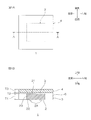
図1A-図1Bを参照して、本発明の第1実施形態の蛍光体層付光半導体素子1(以下、層付素子ともいう。)について説明する。
なお、層付素子1は、光半導体装置16(発光装置;符号は、図2G参照。)ではなく、つまり、光半導体装置16に備えられるダイオード基板15(電極基板;符号は、図2G参照。)を含んでいない。具体的には、層付素子1は、光半導体素子2と、白色層3と、蛍光体層4とを備える。層付素子1は、好ましくは、光半導体素子2、白色層3および蛍光体層4からなる。つまり、層付素子1は、光半導体装置16のダイオード基板15に備えられる電極とまだ電気的に接続されないように、構成されている。また、層付素子1は、光半導体装置16の一部品、すなわち、光半導体装置16を作製するための部品であり、部品単独で流通し、産業上利用可能なデバイスである。
図1A-図1Bに示すように、層付素子1は、光半導体素子2と、白色層3と、蛍光体層4とを備えている。
光半導体素子2は、例えば、電気エネルギーを光エネルギーに変換するLED(発光ダイオード素子)またはLD(半導体レーザー素子)である。好ましくは、光半導体素子2は、青色光を発光する青色LEDである。なお、光半導体素子2は、光半導体素子とは技術分野が異なるトランジスタなどの整流器(半導体素子)を含まない。
光半導体素子2は、左右方向および前後方向に沿う略平板形状を有している。また、光半導体素子2は、平面視略矩形状(好ましくは、平面視略正方形状)を有している。光半導体素子2は、発光面21と、対向面22と、側面23とを備えている。
発光面21は、光半導体素子2における上面である。発光面21は、平坦な形状を有している。発光面21の上には、白色膜5(後述)が設けられている。
対向面22は、光半導体素子2における下面であって、電極24が設けられている面である。対向面22は、発光面21に対して下側に間隔を隔てて対向配置されている。電極24は、複数(2個)設けられており、対向面22から下側に向かってわずかに突出する形状を有している。
側面23は、発光面21の周端縁と、対向面22の周端縁とを連結している。
光半導体素子2の寸法は、適宜設定されており、具体的には、厚みT1(上下方向長さ)は、例えば、0.1μm以上、好ましくは、1μm以上、より好ましくは、10μm以上であり、また、例えば、500μm以下、好ましくは、200μm以下である。光半導体素子2の左右方向および/または前後方向における長さは、それぞれ、例えば、200μm以上、好ましくは、500μm以上であり、また、例えば、3000μm以下、好ましくは、2000μm以下である。
白色層3は、光半導体素子2の上側および側方に配置され、光半導体素子2から主として側方に放射される光を反射することができる白色の反射層である。具体的には、白色層3は、光半導体素子の発光面21および側面23と接触し、それらを被覆している。また、白色層3は、蛍光体層4の下側に配置されている。具体的には、白色層3は、蛍光体層4の下面と接触し、それを被覆している。
白色層3は、白色膜5、および、白色部としての白色側部6を一体的に備えている。
白色膜5は、光半導体素子2の発光面21の上側に配置されている。具体的には、白色膜5は、その下面全面が、発光面21全面の上面全面と接触し、その上面全面が、蛍光体層4の下面の一部(中央部)と接触するように、光半導体素子2と蛍光体層4との間に配置されている。
白色膜5は、左右方向および前後方向に沿う略平板形状を有し、平面視略矩形状(好ましくは、平面視略正方形状)を有している。白色膜5は、厚み方向に投影したときに、発光面21と一致するように形成されている。
白色膜5の厚みT2は、2μm以上15μm以下である。明るさ、放熱性などの観点から、好ましくは、4μm以上であり、また、好ましくは、7μm以下である。
光半導体素子2の厚みT1に対する、白色膜5の厚みT2の比(T2/T1)は、例えば、0.001以上、好ましくは、0.005以上であり、また、例えば、0.300以下、好ましくは、0.200以下である。
白色側部6は、白色膜5および光半導体素子2の側方(周囲、すなわち、左右方向外側および前後方向外側)に、配置されている。具体的には、白色側部6は、白色膜5の周端面全面、および、光半導体素子2の側面23全面と接触するように、配置されている。
白色側部6は、平面視略矩形枠状を有している。白色側部6は、厚み方向に投影したときに、その内形が光半導体素子2の形状と一致し、その外形が蛍光体層4の形状と一致するように形成されている。
白色側部6の厚みは、光半導体素子2の厚みT1および白色膜5の厚みT2の合計と同一である。
白色層3は、100μm厚みとして450nm波長の光で照射したときの反射率が、例えば、70%以上、好ましくは、80%以上、より好ましくは、90%以上であり、また、例えば、100%以下である。反射率を上記範囲内とすることにより、光の取り出し効率を良好にすることができる。反射率の測定方法は、紫外可視近赤外分光光度計を用いて、積分球における光路確認方法にて、450nm波長での反射率を測定することにより求めることができる。
白色層3は、例えば、白色粒子および樹脂を含有する白色樹脂組成物から形成(調製)されている。好ましくは、白色層3は、白色粒子と樹脂とからなる白色樹脂組成物から形成されている。
白色粒子としては、例えば、白色無機粒子、白色有機粒子が挙げられる。好ましくは、放熱性、耐久性の観点から、白色無機粒子が挙げられる。
白色無機粒子を構成する材料としては、例えば、酸化チタン、酸化亜鉛、酸化ジルコニウム、酸化アルミニウムなどの酸化物、例えば、鉛白(塩基性炭酸鉛)、炭酸カルシウムなどの炭酸塩、例えば、カオリンなどの粘土鉱物などが挙げられる。明るさ、放熱性の観点から、好ましくは、酸化物が挙げられ、より好ましくは、酸化チタンが挙げられる。
白色粒子の平均粒子径は、例えば、0.1μm以上、好ましくは、0.2μm以上であり、また、例えば、2.0μm以下、好ましくは、0.5μm以下である。白色粒子の平均粒子径を上記範囲内とすることにより、反射性をより一層向上させることができる。
本発明において、粒子の平均粒子径は、D50値として算出され、具体的には、レーザー回折式粒度分布計により測定される。
白色粒子の含有割合は、白色樹脂組成物に対して、例えば、3質量%以上、好ましくは、5質量%以上、より好ましくは、10質量%以上であり、また、例えば、70質量%以下、好ましくは、50質量%以下、より好ましくは、40質量%以下である。
樹脂は、白色樹脂組成物において白色粒子を均一に分散させるマトリクスであり、好ましくは、透明樹脂である。樹脂としては、例えば、硬化性樹脂、熱可塑性樹脂が挙げられる。好ましくは、硬化性樹脂が挙げられる。
硬化性樹脂としては、例えば、シリコーン樹脂、エポキシ樹脂、ウレタン樹脂、ポリイミド樹脂、フェノール樹脂、尿素樹脂、メラミン樹脂、不飽和ポリエステル樹脂などが挙げられる。
硬化性樹脂としては、2段反応硬化性樹脂、1段反応硬化性樹脂などの熱硬化性樹脂が挙げられる。
2段反応硬化性樹脂は、2つの反応機構を有しており、第1段の反応で、Aステージ状態からBステージ化(半硬化)し、次いで、第2段の反応で、Bステージ状態からCステージ化(完全硬化)することができる。つまり、2段反応硬化性樹脂は、適度の加熱条件によりBステージ状態となることができる熱硬化性樹脂である。Bステージ状態(半硬化状態)は、熱硬化性樹脂が、液状であるAステージ状態(未硬化状態)と、完全硬化したCステージ状態(完全硬化状態)との間の状態であって、硬化およびゲル化がわずかに進行し、圧縮弾性率がCステージ状態の圧縮弾性率よりも小さい半固体状態または固体状態である。
1段反応硬化性樹脂は、1つの反応機構を有しており、第1段の反応で、Aステージ状態からCステージ化することができる。このような1段反応硬化性樹脂は、第1段の反応の途中で、その反応が停止して、Aステージ状態からBステージ状態となることができ、その後のさらなる加熱によって、第1段の反応が再開されて、Bステージ状態からCステージ化することができる熱硬化性樹脂を含む。つまり、1段反応硬化性樹脂は、Bステージ状態となることができる熱硬化性樹脂を含む。また、1段反応硬化性樹脂は、1段の反応の途中で停止するように制御できず、つまり、Bステージ状態となることができず、一度に、AステージからCステージ化する熱硬化性樹脂も含む。
好ましくは、熱硬化性樹脂としては、Bステージ状態となることができる熱硬化性樹脂(2段反応硬化性樹脂および1段反応硬化性樹脂)が挙げられる。
Bステージ状態となることができる熱硬化性樹脂としては、好ましくは、シリコーン樹脂、エポキシ樹脂が挙げられ、より好ましくは、シリコーン樹脂が挙げられる。
また、Bステージ状態となることができるシリコーン樹脂としては、例えば、熱可塑性および熱硬化性を併有するシリコーン樹脂(熱可塑性・熱硬化性シリコーン樹脂)、熱可塑性を有さず・熱硬化性を有するシリコーン樹脂(非熱可塑性・熱硬化性シリコーン樹脂)が挙げられる。
熱可塑性・熱硬化性シリコーン樹脂は、Bステージにおいて、加熱により、一旦可塑化(あるいは液状化)し、その後、さらなる加熱によって硬化(Cステージ化)する。具体的には、1段反応硬化型樹脂として、例えば、特開2016-37562号公報などに記載されるフェニル系シリコーン樹脂組成物が挙げられ、2段反応硬化型樹脂として、例えば、特開2014-72351号公報、特開2013-187227号公報に記載される第1~第6の熱可塑性・熱硬化性シリコーン樹脂組成物(例えば、両末端アミノ型シリコーン樹脂を含有する組成物、かご型オクタシルセスキオキサンを含有する組成物)などが挙げられる。
フェニル系シリコーン樹脂組成物は、シロキサン結合である主骨格にフェニル基を有している。フェニル系シリコーン樹脂組成物としては、好ましくは、付加反応硬化型シリコーン樹脂組成物が挙げられる。具体的には、アルケニル基含有ポリシロキサンと、ヒドロシリル基含有ポリシロキサンと、ヒドロシリル化触媒とを含有し、アルケニル基含有ポリシロキサンおよびヒドロシリル基含有ポリシロキサンの少なくとも一方がフェニル基を有する付加反応硬化型シリコーン樹脂組成物などが挙げられる。
フェニル系シリコーン樹脂組成物としては、上記公報に記載のフェニル系シリコーン樹脂組成物以外にも、ダウ・コーニング社の「OE-6630」などが挙げられる。
非熱可塑性・熱硬化性シリコーン樹脂としては、2段反応硬化型樹脂として、例えば、特開2010-265436号公報、特開2013-187227号公報などに記載される第1~第8の縮合・付加反応硬化型シリコーン樹脂組成物が挙げられる。
所望厚みの白色膜5を均一に形成できる観点から、好ましくは、熱可塑性・熱硬化性シリコーン樹脂が挙げられ、より好ましくは、フェニル系シリコーン樹脂組成物が挙げられる。
また、Bステージ状態をとらない熱硬化性シリコーン樹脂としては、例えば、ELASTOSILシリーズ(旭化成ワッカーシリコーン社製、具体的には、ELASTOSIL LR7665)、KERシリーズ(信越シリコーン社製)などのメチル系シリコーン樹脂組成物などが挙げられる。
樹脂は、単独で使用または2種以上を併用することができる。
樹脂の含有割合は、白色粒子(および後述する添加剤)の含有割合の残部であり、例えば、白色樹脂組成物に対して、例えば、30質量%以上、好ましくは、50質量%以上、より好ましくは、60質量%以上であり、また、例えば、97質量%以下、好ましくは、95質量%以下、より好ましくは、90質量%以下である。
白色樹脂組成物には、白色粒子以外の粒子を含有することができる。
このような粒子としては、例えば、光拡散性無機粒子が挙げられる。光拡散性無機粒子としては、例えば、シリカ粒子、複合無機酸化物粒子(ガラス粒子など)が挙げられる。
複合無機酸化物粒子は、例えば、シリカ、あるいは、シリカおよび酸化ホウ素を主成分として含有し、また、酸化アルミニウム、酸化カルシウム、酸化亜鉛、酸化ストロンチウム、酸化マグネシウム、酸化ジルコニウム、酸化バリウム、酸化アンチモンなどを副成分として含有する。複合無機酸化物粒子における主成分の含有割合は、複合無機酸化物粒子に対して、例えば、40質量%以上、好ましくは、50質量%以上であり、また、例えば、90質量%以下、好ましくは、80質量%以下である。副成分の含有割合は、上記した主成分の含有割合の残部である。
光拡散性無機粒子としては、放熱性、明るさの観点から、好ましくは、シリカ粒子が挙げられる。
光拡散性無機粒子の平均粒子径は、好ましくは、白色粒子の平均粒子径よりも大きく、具体的には、例えば、1.0μm以上、好ましくは、2.0μm以上であり、また、例えば、10μm以下、好ましくは、5.0μm以下、より好ましくは、3.0μm以下である。
光拡散性無機粒子の含有割合は、例えば、白色樹脂組成物に対して、例えば、1質量%以上、好ましくは、5質量%以上、より好ましくは、10質量%以上であり、また、例えば、70質量%以下、好ましくは、50質量%以下、より好ましくは、30質量%以下である。
白色樹脂組成物が光拡散性無機粒子を含有することにより、樹脂の含有量を低減しつつ、放熱性を向上させることができる。なお、白色樹脂組成物に含有される粒子の総量が同一である場合においては、放熱性などの観点から、粒子は、白色粒子のみからなることが好ましい、すなわち、白色粒子以外の粒子を含有しないことが好ましい。
白色樹脂組成物には、公知の添加剤を適宜の割合で含有することもできる。
蛍光体層4は、蛍光体を含有する層であり、白色膜5の上側に配置されている。具体的には、蛍光体層4は、蛍光体層4の下面全面が白色層3(白色膜5および白色側部6)の上面全面と接触するように、白色層3の上面に配置されている。
蛍光体層4は、左右方向および前後方向に沿う略平板形状を有し、平面視略矩形状(好ましくは、平面視略正方形状)を有している。蛍光体層4は、上下方向に投影したときに、白色層3と一致するように形成されている。すなわち、蛍光体層4の周側面は、白色側部6の周側面と面一となっている。
蛍光体層4の厚みT3は、例えば、30μm以上、好ましくは、50μm以上であり、また、例えば、500μm以下、好ましくは、200μm以下である。
蛍光体層4の厚みT3に対する、白色膜5の厚みT2の比(T2/T3)は、例えば、0.004以上、好ましくは、0.01以上であり、また、例えば、0.5以下、好ましくは、0.3以下である。
蛍光体層4は、例えば、シート状の蛍光体含有硬化樹脂からなるか、または、蛍光体セラミックプレートからなる。
蛍光体含有硬化樹脂は、例えば、蛍光体および硬化性樹脂を含有する蛍光体樹脂組成物の完全硬化物(Cステージ状態)である。
蛍光体は、光半導体素子2から発光される光を波長変換する。蛍光体としては、例えば、青色光を黄色光に変換することのできる黄色蛍光体、青色光を赤色光に変換することのできる赤色蛍光体などが挙げられる。
黄色蛍光体としては、例えば、(Ba,Sr,Ca)2SiO4;Eu、(Sr,Ba)2SiO4:Eu(バリウムオルソシリケート(BOS))などのシリケート蛍光体、例えば、Y3Al5O12:Ce(YAG(イットリウム・アルミニウム・ガーネット):Ce)、Tb3Al3O12:Ce(TAG(テルビウム・アルミニウム・ガーネット):Ce)などのガーネット型結晶構造を有するガーネット型蛍光体、例えば、Ca-α-SiAlONなどの酸窒化物蛍光体などが挙げられる。
赤色蛍光体としては、例えば、CaAlSiN3:Eu、CaSiN2:Euなどの窒化物蛍光体などが挙げられる。
蛍光体含有硬化樹脂に含有される蛍光体は、粒子であって、その形状としては、例えば、球状、板状、針状などが挙げられる。
蛍光体の最大長さの平均値(球状である場合には、平均粒子径)は、例えば、0.1μm以上、好ましくは、1μm以上であり、また、例えば、200μm以下、好ましくは、100μm以下である。
蛍光体は、単独で使用または2種以上を併用することができる。
蛍光体の含有割合は、蛍光体樹脂組成物に対して、例えば、10質量%以上、好ましくは、20質量%以上であり、また、例えば、80質量%以下、好ましくは、70質量%以下である。
硬化性樹脂は、蛍光体樹脂組成物において蛍光体を均一に分散させるマトリクスである。このような硬化性樹脂は、白色樹脂組成物で例示した硬化性樹脂と同様の硬化性樹脂が挙げられ、好ましくは、シリコーン樹脂が挙げられ、より好ましくは、熱可塑性・熱硬化性シリコーン樹脂が挙げられ、さらに好ましくは、フェニル系シリコーン樹脂組成物が挙げられる。
硬化性樹脂の含有割合は、蛍光体(および添加剤)の含有割合の残部であり、蛍光体樹脂組成物に対して、例えば、20質量%以上、好ましくは、30質量%以上であり、また、例えば、90質量%以下、好ましくは、80質量%以下である。
蛍光体樹脂組成物には、無機粒子などの公知の添加剤を、適宜の割合で含有することもできる。
無機粒子としては、例えば、白色樹脂組成物にて上述した光拡散性無機粒子が挙げられ、好ましくは、シリカ粒子、ガラス粒子が挙げられ、より好ましくは、ガラス粒子が挙げられる。
無機粒子を含有する場合、その含有割合は、例えば、蛍光体樹脂組成物に対して、例えば、1質量%以上、好ましくは、5質量%以上、より好ましくは、10質量%以上であり、また、例えば、70質量%以下、好ましくは、50質量%以下、より好ましくは、30質量%以下である。
蛍光体セラミックプレートは、上記した蛍光体をセラミック材料とし、上記したセラミック材料を焼結することにより、得られる。または、上記した蛍光体の原材料を焼結し、焼結による化学反応によっても、得られる。
<第1実施形態の製造方法>
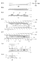
図2A-図2Gを参照して、第1実施形態の層付素子1の製造方法を説明する。第1実施形態の層付素子1の製造方法は、例えば、蛍光体積層シート用意工程、仮固定シート用意工程、仮固定工程、対向配置工程、積層工程、Cステージ化工程、および、切断工程を備える。
図2A-図2Gを参照して、第1実施形態の層付素子1の製造方法を説明する。第1実施形態の層付素子1の製造方法は、例えば、蛍光体積層シート用意工程、仮固定シート用意工程、仮固定工程、対向配置工程、積層工程、Cステージ化工程、および、切断工程を備える。
まず、図2Aに示すように、蛍光体積層シート用意工程では、蛍光体積層シート10を用意する。
蛍光体積層シート10は、蛍光体層4と、蛍光体層4の上面に配置される白色層3とを備えている。蛍光体積層シート10における白色層3は、Bステージ状態である。
蛍光体積層シート10の作製は、例えば、まず、蛍光体層4を形成し、次いで、蛍光体層4の上面に白色層3を積層する。
蛍光体層4の形成は、例えば、蛍光体層4が蛍光体含有硬化樹脂からなる場合は、蛍光体および硬化性樹脂を含有する蛍光体樹脂組成物のワニスを調製し、続いて、蛍光体樹脂組成物のワニスを、剥離シートの上面に塗布する。次いで、蛍光体樹脂組成物をCステージ化(完全硬化)する。具体的には、硬化性樹脂が熱硬化性樹脂である場合には、蛍光体樹脂組成物を加熱する。
加熱温度は、例えば、100℃以上、好ましくは、120℃以上であり、また、例えば、200℃以下、好ましくは、160℃以下である。また、加熱時間は、例えば、5分以上、好ましくは、10分以上であり、また、例えば、60分以下、好ましくは、30分以下である。
蛍光体層4が蛍光体セラミックプレートである場合は、例えば、蛍光体材料、バインダー樹脂および溶媒を含むスラリーを剥離シートの上面に塗布および乾燥させることにより、グリーンシートを形成し、続いて、グリーンシートを焼成する。スラリーの材料や焼成条件は、例えば、特開2015-216355号公報などを参照することができる。
得られる蛍光体層4の25℃における引張弾性率Eは、例えば、1MPa以上、好ましくは、3MPa以上、より好ましくは、10MPa以上であり、また、例えば、150MPa以下、好ましくは、100MPa以下、より好ましくは、50MPa以下である。引張弾性率Eを上記下限以上とすることにより、層付素子1の蛍光体層4の形状安定性を良好にすることができ、その結果、明るさを良好にすることができる。一方、引張弾性率Eを上記上限以下とすることにより、蛍光体層4に適度な可撓性を付与し、層付素子1を製造する際に、蛍光体層4にクラックの発生を抑制することができる。
上記引張弾性率Eは、蛍光体層4に対して、引張速度300mm/minの条件で測定することにより求められる。
白色層3の積層は、まず、Bステージ状態となることができる白色樹脂組成物を調製する。具体的には、白色粒子、および、Bステージ状態となることができる熱硬化性樹脂を含有する白色樹脂組成物のワニスを調製する。好ましくは、白色粒子、および、熱可塑性・熱硬化性シリコーン樹脂組成物を含有する白色樹脂組成物のワニスを調製する。
続いて、その白色樹脂組成物のワニスを蛍光体層4の上面に塗布する。その後、白色樹脂組成物をBステージ化する。具体的には、白色樹脂組成物を加熱する。
塗布方法としては限定されず、例えば、アプリケータを用いる方法、ポッティング、キャストコート、スピンコート、ロールコートなどが挙げられる。
加熱温度は、白色樹脂組成物がBステージ化されるが、Cステージ化されない範囲で、白色樹脂組成物の組成、および、白色樹脂組成物の溶融粘度に応じて適宜設定され、例えば、50℃以上、好ましくは、60℃以上であり、また、例えば、120℃以下、好ましくは、100℃以下である。
加熱時間は、例えば、3分以上、好ましくは、5分以上であり、また、例えば、120分以下、好ましくは、60分以下である。
これによって、Bステージ状態の白色層3が得られる。好ましくは、この白色層3は、熱可塑性および熱硬化性を併有する。
Bステージ状態の白色層3の60℃における溶融粘度は、例えば、5Pa・s以上、好ましくは、10Pa・s以上、より好ましくは、15Pa・s以上であり、また、例えば、800Pa・s以下、好ましくは、600Pa・s以下、より好ましくは、550Pa・s以下である。白色層3の溶融粘度を上記下限以上とすることにより、白色層3のハンドリング性を向上させることができる。また、白色層3の溶融粘度を上記上限以下とすることにより、白色層3の成形性が良好となる。また、層付素子1の白色膜5の厚さ調整を容易にし、所望の膜厚(2~15μm)を得ることができる。
溶融粘度は、Bステージの白色層3を60℃に温度調節し、E型コーンを用いて測定することにより、求められる。回転数は、例えば、トルクが30~90%の範囲となるように選択する。また、白色層3が60℃に均一に加熱されて、測定される粘度が一定となった後の粘度、具体的には、測定開始3分経過後の値を採用する。
蛍光体積層シート10における白色層3の厚みは、光半導体素子2の厚みと同一かそれよりもわずかに厚く、具体的には、0.1μm以上、好ましくは、1μm以上、より好ましくは、5μm以上であり、また、例えば、800μm以下、好ましくは、500μm以下、より好ましくは、200μm以下である。
蛍光体積層シート10において、蛍光体層4の厚みに対する、白色層3の厚みの比(白色層/蛍光体層)は、例えば、1以上、好ましくは、2以上であり、また、例えば、10以下、好ましくは、8以下である。
一方、図2Bに示すように、仮固定シート用意工程では、仮固定シート11をキャリア12の上面に配置する。
仮固定シート11は、例えば、両面に感圧接着性を備えるシートであり、例えば、配列テープや両面テープとして、公知または市販のものを用意できる。仮固定シート11は、例えば、単一の感圧接着剤層から形成されている単層構造を有していてもよく、また、支持基材の両面に感圧接着剤層が積層されている複層構造を有していてもよい。感圧接着剤層は、例えば、処理(例えば、紫外線の照射や加熱など)によって感圧接着力が低減するような感圧接着剤から形成されている。
キャリア12は、仮固定シート11を下方から支持すための支持板であり、例えば、硬質材料からなる。硬質材料としては、例えば、ガラス、セラミック、ステンレスなどが挙げられる。
次いで、図2Cに示すように、仮固定工程では、複数の光半導体素子2を、仮固定シート11の上に仮固定する。
具体的には、複数の光半導体素子2の電極24を、仮固定シート42の上面に感圧接着させる。このとき、複数の光半導体素子2を、仮固定シートの上に、左右方向および前後方向に互いに間隔を隔てて、整列配置させる。
これによって、キャリア12と、キャリア12の上側に配置される仮固定シート11と、仮固定シート11の上に整列配置される複数の光半導体素子2とを備える素子配置キャリア13が得られる。
次いで、図2Dに示すように、対向配置工程では、素子配置キャリア13および蛍光体積層シート10を、上下方向に間隔を隔てて対向配置する。
具体的には、素子配置キャリア13および蛍光体積層シート10をプレス機30にセットする。
プレス機30は、熱源を備える熱プレス機であって、下板31と、下板31の上側に配置され、下板31に対して下側に移動可能に構成される上板32と、下板31の上面に載置され、熱プレス時における上板32および下板31の間隔を調整するためのスペーサ33とを備える。
そして、白色層3が上側となるように、下板31の上面に蛍光体積層シート10を配置する。一方、光半導体素子2が下側となるように、上板32の下面に素子配置キャリア13を固定する。
また、スペーサ33は、熱プレス時に、光半導体素子2の発光面21が、蛍光体層4の白色層側表面に達するように、すなわち、発光面21が蛍光体層4と白色層3との界面付近に達するように、調整する。
次いで、図2Eに示すように、積層工程では、蛍光体積層シート10を、素子配置キャリア13に積層する。
具体的には、プレス機30の熱源を作動させながら上板32を下方に移動することにより、熱プレスを実施する。
このとき、スペーサ33を適宜調整することにより、光半導体素子2を、白色層3に埋没させ、光半導体素子2の発光面21を、蛍光体層4の白色層側表面(上面)付近に到達させる。これにより、白色層3が、熱可塑性・熱硬化性シリコーン樹脂組成物を含有する場合、白色層3は、熱により容易に溶融するため、発光面21と蛍光体層4の白色層側表面との僅かな隙間(界面)に均一にかつ薄く濡れ広がるように形成される。その後、熱硬化反応によって、所望厚み(2~15μm)の白色膜5が形成される。
熱プレスの圧力は、例えば、0.01MPa以上、好ましくは、0.1MPa以上であり、また、例えば、10MPa以下、好ましくは、5MPa以下である。
熱プレスの温度は、白色層3を溶融させる温度であればよく、例えば、40℃以上、好ましくは、45℃以上、より好ましくは、50℃以上であり、また、例えば、180℃以下、好ましくは、150℃以下、より好ましくは、100℃未満である。
加熱プレスの時間は、例えば、1秒以上、好ましくは、3秒以上であり、また、例えば、30分以下、好ましくは、10分以下である。
これによって、複数の光半導体素子2と、白色層3と、蛍光体層4とを備える層付素子集合体14が、仮固定シート11に仮固定された状態で、得られる。
次いで、Cステージ化工程では、Bステージ状態の白色層3をCステージ化する。
具体的には、加熱工程を実施する。すなわち、層付素子集合体14をプレス機30から取り出し、オーブンなどによって、加熱する。
加熱温度は、例えば、100℃以上、好ましくは、120℃以上、より好ましくは、130℃以上であり、また、例えば、200℃以下、好ましくは、160℃以下、より好ましくは、150℃以下である。また、加熱時間は、例えば、10分以上、好ましくは、30分以上、より好ましくは、60分以上であり、また、例えば、480分以下、好ましくは、300分以下、より好ましくは、180分以下である。なお、加熱を、異なる温度で複数回実施することもできる。
次いで、図2Fに示すように、切断工程では、層付素子集合体14を切断する。
具体的には、図2Fの破線が示すように、隣接する光半導体素子2の間における白色層3および蛍光体層4を、ダイシングなどによって切断する。これによって、層付素子集合体14を個片化する。
これによって、1つの光半導体素子2と、白色層3と、蛍光体層4とを備える層付素子1が、仮固定シート11に仮固定された状態で、得られる。
続いて、図2Fの仮想線が示すように、層付素子1を仮固定シート11から引き剥がす。
続いて、必要に応じて、対向面22を被覆する白色層3を、対向面22(電極)が露出するように、グラインド加工する。
これによって、1つの光半導体素子2と、白色層3と、蛍光体層4とを備える層付素子1が、得られる。
なお、図2Gに示すように、層付素子1を、ダイオード基板15などの電極基板にフリップチップ実装することにより、発光ダイオード装置などの光半導体装置16が得られる(実装工程)。
ダイオード基板15は、略平板形状を有し、具体的には、絶縁基板の上面に、導体層が回路パターンとして積層された積層板から形成されている。絶縁基板は、例えば、シリコン基板、セラミックス基板、プラスチック基板(例えば、ポリイミド樹脂基板)などからなる。導体層は、例えば、金、銅、銀、ニッケルなどの導体から形成されている。導体層は、単数の光半導体素子2と電気的に接続するための電極(図示せず)を備えている。ダイオード基板15の厚みは、例えば、25μm以上、好ましくは、50μm以上であり、また、例えば、2000μm以下、好ましくは、1000μm以下である。
<作用効果>
第1実施形態の層付素子1では、半導体素子2と、発光面21に配置される白色膜5と、白色膜5の上面に配置される蛍光体層4とを備え、白色膜5の厚みが、2μm以上15μm以下である。このため、光半導体素子2と蛍光体層4との密着性が良好であり、接合信頼性に優れる。また、蛍光体層4で生じる熱を、白色膜5を介して放熱できるため、放熱性に優れる。また、蛍光体層4の放熱性が優れることにより、長時間発光させた際に、蛍光体層4の温度負荷によるクラックの発生を抑制することができ、耐久信頼性にも優れる。さらに、白色膜5の厚みが薄いため、発光面21から蛍光体層4に入る光の吸収および反射を低減でき、明るさの低下を抑制することができる。
第1実施形態の層付素子1では、半導体素子2と、発光面21に配置される白色膜5と、白色膜5の上面に配置される蛍光体層4とを備え、白色膜5の厚みが、2μm以上15μm以下である。このため、光半導体素子2と蛍光体層4との密着性が良好であり、接合信頼性に優れる。また、蛍光体層4で生じる熱を、白色膜5を介して放熱できるため、放熱性に優れる。また、蛍光体層4の放熱性が優れることにより、長時間発光させた際に、蛍光体層4の温度負荷によるクラックの発生を抑制することができ、耐久信頼性にも優れる。さらに、白色膜5の厚みが薄いため、発光面21から蛍光体層4に入る光の吸収および反射を低減でき、明るさの低下を抑制することができる。
また、光半導体素子2の周囲に配置される白色側部6をさらに備えている。このため、光半導体素子2の側方から放射される光を反射することができ、明るさが良好である。また、放熱性にも優れる。
<第1実施形態の変形例>
第1実施形態の変形例において、第1実施形態と同じ部材および工程については、同一の参照符号を付し、その詳細な説明を省略する。
第1実施形態の変形例において、第1実施形態と同じ部材および工程については、同一の参照符号を付し、その詳細な説明を省略する。
図1A-図2Bに示す第1実施形態では、蛍光体層4の上面は露出しているが、例えば、図3に示すように、蛍光体層4の上面に光拡散層40などの機能層を配置することもできる。
光拡散層40は、蛍光体層4から上側に向かって放出される光を左右方向および前後方向に拡散させる層である。光拡散層40は、左右方向および前後方向に沿う略平板形状を有しており、平面視において、蛍光体層4と同一形状となるように形成されている。光拡散層40は、例えば、白色樹脂組成物において上記した光拡散性無機粒子および樹脂を含有する光拡散性樹脂組成物から形成することができる。
<第1実施形態の製造方法の変形例>
図2A-図2Gに示す第1実施形態の製造方法では、蛍光体積層シート10を用いて層付素子1を製造しているが、例えば、図4A-図5Hに示すように、蛍光体積層シート10を形成せずに層付素子1を製造することができる。
図2A-図2Gに示す第1実施形態の製造方法では、蛍光体積層シート10を用いて層付素子1を製造しているが、例えば、図4A-図5Hに示すように、蛍光体積層シート10を形成せずに層付素子1を製造することができる。
図4A-図5Hに示す実施形態では、仮固定シート用意工程、仮固定工程、白色樹脂組成物配置工程、白色層積層工程、厚み調整工程、蛍光体層積層工程、Cステージ化工程、および、切断工程を備える。
まず、図4A-図4Bに示すように、仮固定シート用意工程および仮固定工程を実施する。仮固定シート用意工程および仮固定工程は、第1実施形態の製造方法と同様である。
次いで、図4Cに示すように、白色樹脂組成物配置工程では、素子配置キャリア13および白色樹脂組成物34を、上下方向に間隔を隔てて対向配置する。
具体的には、素子配置キャリア13および白色樹脂組成物34をプレス機30にセットする。
まず、プレス機30の下板31の上面に、白色樹脂組成物34を配置する。具体的には、平面視枠状のスペーサ33を下板31の上面に配置し、続いて、下板31の上面およびスペーサ33の内側表面に、上側が開放する箱形状を有する剥離シート35を配置し、続いて、剥離シート35内部にAステージの白色樹脂組成物34を充填する。
一方、光半導体素子2が下側となるように、上板32の下面に、素子配置キャリア13を固定する。
次いで、図4Dに示すように、白色層積層工程では、素子配置キャリア13に白色層3を積層する。
具体的には、熱プレスを実施する。熱プレスの条件としては、第1実施形態と同様である。
これにより、光半導体素子2が白色樹脂組成物34に埋没され、また、白色樹脂組成物34がBステージ化されて、Bステージ状態の白色層3が形成される。すなわち、光半導体素子2が白色層3によって被覆される。
これによって、図4Eに示すように、複数の光半導体素子2と、白色層(Bステージ)3とを備える白色層付素子の集合体17が、仮固定シート11に仮固定された状態で、得られる。
次いで、図4Fに示すように、厚み調整工程では、白色層3の厚みを調整する。
具体的には、白色層3の上側部分、すなわち、白色膜5の上部を厚み方向に除去する。
除去方法としては、例えば、(1)感圧接着シートを白色膜5の上面に貼着した後、引き剥がす方法、(2)溶媒を含浸した布を用いて、白色膜5の上面を拭き取る方法、(3)バス、ブラシ、ブラストなどの研磨部材を用いて、白色膜5の上面を研磨する方法などが挙げられる。
これによって、白色膜5の厚みが2μm以上15μm以下となるように調整される。
次いで、図5Gに示すように、蛍光体層積層工程では、白色層付素子の集合体17の白色層3に、蛍光体層4を積層する。
具体的には、熱プレスを実施する。熱プレスの条件としては、上記白色層積層工程と同様である。
これによって、複数の光半導体素子2と、白色層3(Bステージ)と、蛍光体層4とを備える層付素子集合体14が、仮固定シート11に仮固定された状態で、得られる。
次いで、Cステージ化工程、および、図5Hの破線が示す切断工程を実施する。Cステージ化工程および切断工程は、第1実施形態と同様である。
これによって、1つの光半導体素子2と、白色層3と、蛍光体層4とを備える層付素子1が、得られる。
本発明では、好ましくは、図2A-図2Gに示す製造方法が挙げられる。図2A-図2Gの製造方法では、熱プレスなどの積層工程や厚み調整工程などの工程数を低減でき、また、白色膜5の厚みを容易に調整することができる。
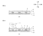
<第2実施形態>
図6を参照して、本発明の層付素子1の第2実施形態について説明する。
図6を参照して、本発明の層付素子1の第2実施形態について説明する。
第2実施形態において、第1実施形態と同じ部材および工程については、同一の参照符号を付し、その詳細な説明を省略する。
図6に示すように、層付素子1は、光半導体素子2と、白色層3と、蛍光体層4とを備えている。
白色層3は、白色膜5および白色側部6を一体的に備えている。
白色膜5は、光半導体素子2の上側および側方に配置され、光半導体素子の上部を被覆している。白色膜5は、下側を開放する箱形状を有し、第1白色膜5aおよび第2白色膜5bを一体的に備えている。
第1白色膜5aは、光半導体素子2の上側に、配置されている。第1白色膜5aは、その下面全面が発光面21全面と接触し、その上面全面が蛍光体層4の下面の一部(中央部)と接触するように、光半導体素子2と、蛍光体層4との間に配置されている。第1白色膜5aは、左右方向および前後方向に沿う略平板形状を有し、平面視略矩形状(好ましくは、平面視略正方形状)を有している。また、第1白色膜5aは、厚み方向に投影したときに、発光面21と一致するように形成されている。
第2白色膜5bは、光半導体素子2の側方に配置されている。具体的には、第2白色膜5bは、光半導体素子2の側面の上部と接触するように、光半導体素子2と、蛍光体層4との間に配置されている。第2白色膜5bは、平面視略矩形枠状を有しており、その上端が第1白色膜5aの周端縁と連続している。
白色膜5の厚み(すなわち、第1白色膜5aの上下方向長さ、および、第2白色膜5bの前後方向長さまたは左右方向長さ)は、2μm以上15μm以下である。好ましくは、4μm以上であり、また、好ましくは、7μm以下である。
第2白色膜5bの厚み(前後方向長さまたは左右方向長さ)は、光半導体素子2の上下方向長さよりも短く、例えば、光半導体素子2の上下方向長さ100%に対して、例えば、10%以上、好ましくは、20%以上であり、また、例えば、95%以下、好ましくは、90%以下である。具体的には、例えば、5μm以上、好ましくは、10μm以上であり、また、例えば、200μm以下、好ましくは、150μm以下である。
白色側部6は、光半導体素子2の下部の側方に、配置されている。具体的には、白色側部6は、光半導体素子2の側面23の下部と接触し、それを被覆している。また、白色側部6の上端は、第2白色膜5bの下端と連続している。
白色側部6は、平面視略矩形枠状を有している。白色側部6は、厚み方向に投影したときに、その内形が光半導体素子2の形状と一致し、その外形が蛍光体層4の形状と一致するように形成されている。
蛍光体層4は、白色層3の上側に配置されている。具体的には、蛍光体層4は、蛍光体層4の下面全面が、白色膜5および白色側部6の上面全面と接触するように、白色膜5および白色側部6の上面に配置されている。
また、蛍光体層4は、断面視において、下側を開放するコ字形状を有し、蛍光体上部7および蛍光体下部8を一体的に備えている。
蛍光体上部7は、白色層3の上側に配置されている。具体的には、蛍光体上部7は、その下面が、第1白色膜5aの上面と接触し、蛍光体下部8の上面と連続するように、配置されている。蛍光体上部7は、左右方向および前後方向に沿う略平板形状を有し、平面視略矩形状(好ましくは、平面視略正方形状)を有している。蛍光体上部7は、厚み方向に投影したときに、発光面21を含むように形成され、かつ、白色側部6の外形と一致するように形成されている。
蛍光体下部8は、光半導体素子2の側方に配置されている。具体的には、蛍光体下部8は、第2白色膜5bの周側面と接触し、それを被覆している。蛍光体下部8は、平面視略枠矩形状を有している。蛍光体下部8は、厚み方向に投影したときに、その内形が第2白色膜5bの外形と一致し、その外形が白色側部6の外形と一致するように形成されている。
第2実施形態の層付素子1は、例えば、図2A-図2Gの製造工程を参照して製造することができる。
特に、図2Aにおいて、白色層3の厚みが光半導体素子2の厚みよりも薄く、蛍光体層4がBステージ状態である蛍光体積層シート10を作製する。
次いで、このような蛍光体積層シート10を用いて、図2D-図2Eに示すように、蛍光体積層シート10を、素子配置キャリア13に積層する。具体的には、プレス機30の熱源を作動させながら上板32を下方に移動することにより、熱プレスを実施する。これにより、白色層3の白色樹脂組成物34が、光半導体素子2の上部(発光面21および上部側面)に濡れ広がって、これらの面に白色膜5が形成(被覆)される。また、光半導体素子2の上部は、白色膜5を被覆したまま、蛍光体層4に埋没される。
次いで、Cステージ化工程および切断工程により、白色層3および蛍光体層4をCステージ化し、個片化して、図6に示す層付素子1が得られる。
以下に実施例および比較例を示し、本発明をさらに具体的に説明するが、本発明は、何ら実施例および比較例に限定されない。以下の記載において用いられる配合割合(含有割合)、物性値、パラメータなどの具体的数値は、上記の「発明を実施するための形態」において記載されている、それらに対応する配合割合(含有割合)、物性値、パラメータなど該当記載の上限値(「以下」、「未満」として定義されている数値)または下限値(「以上」、「超過」として定義されている数値)に代替することができる。
(蛍光体樹脂組成物Aの調製)
特開2016-37562号公報の実施例に記載の調製例1に準拠して、フェニル系シリコーン樹脂組成物(Bステージ状態となることができる1段反応硬化性樹脂、熱可塑性・熱硬化性シリコーン樹脂、付加反応硬化型)を調製した。
特開2016-37562号公報の実施例に記載の調製例1に準拠して、フェニル系シリコーン樹脂組成物(Bステージ状態となることができる1段反応硬化性樹脂、熱可塑性・熱硬化性シリコーン樹脂、付加反応硬化型)を調製した。
このフェニル系シリコーン樹脂組成物100質量部に、黄色系蛍光体(「Y-468」、根本特殊化学社製)40質量部を混合して、蛍光体樹脂組成物Aを調製した。
(蛍光体樹脂組成物Bの調製)
特開2016-37562号公報の実施例に記載の調製例1に準拠して、フェニル系シリコーン樹脂組成物を調製した。このフェニル系シリコーン樹脂組成物100質量部に、黄色系蛍光体(上記と同様)40質量部およびガラス粒子50質量部を混合して、蛍光体樹脂組成物Bを調製した。
特開2016-37562号公報の実施例に記載の調製例1に準拠して、フェニル系シリコーン樹脂組成物を調製した。このフェニル系シリコーン樹脂組成物100質量部に、黄色系蛍光体(上記と同様)40質量部およびガラス粒子50質量部を混合して、蛍光体樹脂組成物Bを調製した。
ガラス粒子としては、SiO2/Al2O3/CaO/MgO=60/20/15/5(質量%)、平均粒子径20μm、屈折率1.55の無機粒子を使用した。
(蛍光体樹脂組成物Cの調製)
メチル系シリコーン樹脂組成物(「KER-2500」、信越化学社製、付加反応硬化型)100質量部に、黄色系蛍光体(上記と同様)40質量部を混合して、蛍光体樹脂組成物Cを調製した。
メチル系シリコーン樹脂組成物(「KER-2500」、信越化学社製、付加反応硬化型)100質量部に、黄色系蛍光体(上記と同様)40質量部を混合して、蛍光体樹脂組成物Cを調製した。
(白色樹脂組成物Aの調製)
特開2016-37562号公報の実施例に記載の調製例1に準拠して、フェニル系シリコーン樹脂組成物(Bステージ状態となることができる1段反応硬化性樹脂、熱可塑性・熱硬化性シリコーン樹脂、付加反応硬化型)を調製した。
特開2016-37562号公報の実施例に記載の調製例1に準拠して、フェニル系シリコーン樹脂組成物(Bステージ状態となることができる1段反応硬化性樹脂、熱可塑性・熱硬化性シリコーン樹脂、付加反応硬化型)を調製した。
フェニル系シリコーン樹脂組成物100質量部に、酸化チタン(白色粒子、「R706S」、デュポン社製、平均粒子径0.36μm)30質量部を混合して、白色樹脂組成物Aを調製した。
(白色樹脂組成物Bの調製)
特開2016-37562号公報の実施例に記載の調製例1に準拠して、フェニル系シリコーン樹脂組成物(上記と同様)を調製した。
特開2016-37562号公報の実施例に記載の調製例1に準拠して、フェニル系シリコーン樹脂組成物(上記と同様)を調製した。
フェニル系シリコーン樹脂組成物100質量部に、酸化チタン(上記と同様)30質量部およびシリカ(光拡散性無機粒子、「DL-7400S」、日本電気硝子社製、平均粒子径2.0μm)10質量部を混合して、白色樹脂組成物Bを調製した。
(白色樹脂組成物Cの調製)
特開2016-37562号公報の実施例に記載の調製例1に準拠して、フェニル系シリコーン樹脂組成物(上記と同様)を調製した。
特開2016-37562号公報の実施例に記載の調製例1に準拠して、フェニル系シリコーン樹脂組成物(上記と同様)を調製した。
フェニル系シリコーン樹脂組成物100質量部に、酸化チタン(上記と同様)30質量部およびシリカ(光拡散性無機粒子、「FB-3SDC」、DENKA社製、平均粒子径3.4μm)10質量部を混合して、白色樹脂組成物Cを調製した。
(実施例1)
まず、蛍光体樹脂組成物Aを剥離シートの上に塗布し、120℃、10分加熱することにより、Cステージ状態の蛍光体層(厚み100μm)を形成した。蛍光体層の引張弾性率Eは、37MPaであった。次いで、蛍光体層の上面に、白色樹脂組成物Aを塗布し、80℃、10分加熱することにより、Bステージ状態の白色層(厚み400μm)を形成した。白色層の溶融粘度(60℃)は、13Pa・sであった(表1参照)。これにより、蛍光体積層シートを得た(図2A参照)。
まず、蛍光体樹脂組成物Aを剥離シートの上に塗布し、120℃、10分加熱することにより、Cステージ状態の蛍光体層(厚み100μm)を形成した。蛍光体層の引張弾性率Eは、37MPaであった。次いで、蛍光体層の上面に、白色樹脂組成物Aを塗布し、80℃、10分加熱することにより、Bステージ状態の白色層(厚み400μm)を形成した。白色層の溶融粘度(60℃)は、13Pa・sであった(表1参照)。これにより、蛍光体積層シートを得た(図2A参照)。
次いで、ステンレスキャリアの上に、仮固定シート(日東電工社製、「リバアルファ」、両面タイプ)を配置した(図2B参照)。
次いで、電極が対向面に設けられた光半導体素子(1.0mm角、厚み150μm、商品名「EDI-FA4545A」、エピスター社製)を複数用意し、光半導体素子を仮固定シートの上に、1.64mmピッチで、前後方向に20個、左右方向に20個、整列配置した(図2C参照)。これにより、素子配置キャリアを得た。
次いで、プレス機に、蛍光体積層シートおよび素子配置キャリアをセットした(図2D参照)。具体的には、プレス機の下板の上面に、蛍光体積層シートを、白色層が上側となるように、配置し、プレス機の上板の下面に、素子配置キャリアを、光半導体素子が下側となるように固定した。また、プレス時に、発光面が、蛍光体層と白色層との界面の高さを位置付近となるように、スペーサを調整した。
次いで、90℃、0.1MPa、10分の条件で、熱プレスを実施した。これにより、層付素子集合体を得た(図2E参照)。
次いで、層付素子集合体を、150℃のオーブンに120分放置することにより、白色層をCステージ化させた。
次いで、隣接する光半導体素子の間における白色層および蛍光体層を、ダイシングによって切断して、層付素子集合体を個片化した。続いて、個片化された層付素子を仮固定シートから引き剥がし、その後、対向面を被覆する白色層を、対向面が露出するように、グラインド加工した(図2F参照)。
これにより、層付素子を製造した。
(実施例2~6)
白色樹脂組成物Aの硬化条件を調整し、白色層の溶融粘度を表1に記載の溶融粘度にした以外は、実施例1と同様にして、層付素子を製造した。
白色樹脂組成物Aの硬化条件を調整し、白色層の溶融粘度を表1に記載の溶融粘度にした以外は、実施例1と同様にして、層付素子を製造した。
(実施例7)
白色樹脂組成物Aの代わりに白色樹脂組成物Bを用いた以外は、実施例1と同様にして、層付素子を製造した。
白色樹脂組成物Aの代わりに白色樹脂組成物Bを用いた以外は、実施例1と同様にして、層付素子を製造した。
(実施例8)
白色樹脂組成物Aの代わりに白色樹脂組成物Cを用いた以外は、実施例1と同様にして、層付素子を製造した。
白色樹脂組成物Aの代わりに白色樹脂組成物Cを用いた以外は、実施例1と同様にして、層付素子を製造した。
(実施例9)
蛍光体樹脂組成物Aの代わりに蛍光体樹脂組成物Bを用い、かつ、白色層の溶融粘度を表1に記載の溶融粘度にした以外は、実施例1と同様にして、蛍光体層シートおよび層付素子を製造した。
蛍光体樹脂組成物Aの代わりに蛍光体樹脂組成物Bを用い、かつ、白色層の溶融粘度を表1に記載の溶融粘度にした以外は、実施例1と同様にして、蛍光体層シートおよび層付素子を製造した。
(実施例10)
蛍光体樹脂組成物Aの代わりに蛍光体樹脂組成物Cを用いた以外は、実施例1と同様にして、蛍光体層シートおよび層付素子を製造した。
蛍光体樹脂組成物Aの代わりに蛍光体樹脂組成物Cを用いた以外は、実施例1と同様にして、蛍光体層シートおよび層付素子を製造した。
(比較例1)
白色樹脂組成物Aおよび蛍光体樹脂組成物Aを用いて、図4A~図5Hに示す工程で実施し、層付素子を製造した。なお、図4Fの厚み調整工程において、発光面の上面に形成された白色膜を完全に除去して、白色膜の厚みを0μmとした。
白色樹脂組成物Aおよび蛍光体樹脂組成物Aを用いて、図4A~図5Hに示す工程で実施し、層付素子を製造した。なお、図4Fの厚み調整工程において、発光面の上面に形成された白色膜を完全に除去して、白色膜の厚みを0μmとした。
(比較例2~3)
白色樹脂組成物Aの硬化条件を調整し、白色層の溶融粘度を表1に記載の溶融粘度にした以外は、実施例1と同様にして、蛍光体層シートを製造した。
白色樹脂組成物Aの硬化条件を調整し、白色層の溶融粘度を表1に記載の溶融粘度にした以外は、実施例1と同様にして、蛍光体層シートを製造した。
(比較例4)
白色樹脂組成物として白色樹脂組成物Aを用い、蛍光体樹脂組成物として蛍光体樹脂組成物Aを用いて、図4A~図5Hに示す工程で実施し、層付素子を製造した。
白色樹脂組成物として白色樹脂組成物Aを用い、蛍光体樹脂組成物として蛍光体樹脂組成物Aを用いて、図4A~図5Hに示す工程で実施し、層付素子を製造した。
ただし、図4Bの仮固定工程後において、発光面に保護テープを貼着し、発光面表面に白色膜が形成されないようにしたため、図4Eに示す厚み調整工程は省略した。また、図5Gの蛍光体層積層工程の前に、白色層付素子の集合体の上面に、厚み5μmの接着剤層(信越化学社製、透明シリコーン樹脂、「KER-2500」)を配置し、その接着剤層の上に蛍光体層を配置した。
すなわち、比較例4の層付素子は、白色膜の代わりに、接着剤層を介して、光半導体素子および白色層と、蛍光体層とを接着させた。
(厚みの測定)
白色膜および蛍光体層の厚みは、測定計(リニアゲージ)により測定した。
白色膜および蛍光体層の厚みは、測定計(リニアゲージ)により測定した。
(蛍光体層の引張弾性率Eの測定)
Cステージの蛍光体層からサンプルを採取して、このサンプルの弾性率を下記の条件で測定し、サンプルの25℃の引張弾性率Eを求めた。
Cステージの蛍光体層からサンプルを採取して、このサンプルの弾性率を下記の条件で測定し、サンプルの25℃の引張弾性率Eを求めた。
装置:引張試験機、「テンシロン」、島津製作所社製
チャック間距離:10mm
引張速度:300mm/分
(白色層の溶融粘度の測定)
Bステージの白色層を、60℃に温度調節したE型粘度計に設置し、E型コーンを用いて測定した。回転数は、トルクが30~90%となるように適宜調整した。なお、溶融粘度は、測定開始後3分後の粘度を記録した。
チャック間距離:10mm
引張速度:300mm/分
(白色層の溶融粘度の測定)
Bステージの白色層を、60℃に温度調節したE型粘度計に設置し、E型コーンを用いて測定した。回転数は、トルクが30~90%となるように適宜調整した。なお、溶融粘度は、測定開始後3分後の粘度を記録した。
(明るさの測定)
各実施例および各比較例の層付素子を、ダイオード基板にフリップチップ実装して、光半導体装置を得た。この光半導体装置に、300mAの電流を通電して、積分球により、明るさ(全光束)を測定した。
各実施例および各比較例の層付素子を、ダイオード基板にフリップチップ実装して、光半導体装置を得た。この光半導体装置に、300mAの電流を通電して、積分球により、明るさ(全光束)を測定した。
実施例1の光半導体装置の明るさ(ミリルーメン)を100%として、各光半導体装置の明るさを求めた。結果を表1に示す。
(放熱性の測定)
各実施例および各比較例の層付素子を、ダイオード基板にフリップチップ実装して、光半導体装置を得た。この光半導体装置に、1000mAの電流を通電したときの蛍光体層表面の温度を、K熱電対を用いて測定した。結果を表1に示す。
各実施例および各比較例の層付素子を、ダイオード基板にフリップチップ実装して、光半導体装置を得た。この光半導体装置に、1000mAの電流を通電したときの蛍光体層表面の温度を、K熱電対を用いて測定した。結果を表1に示す。
(接合信頼性の測定)
各実施例および各比較例の層付素子の下部(白色層および光半導体素子)を台に固定し、蛍光体層の側面を面方向に押した。このときの蛍光体層と光半導体素子との接着性を下記のように評価した。結果を表1に示す。
各実施例および各比較例の層付素子の下部(白色層および光半導体素子)を台に固定し、蛍光体層の側面を面方向に押した。このときの蛍光体層と光半導体素子との接着性を下記のように評価した。結果を表1に示す。
蛍光体層が、光半導体素子に対して、面方向に容易にずれた場合を×と評価した。蛍光体層が、光半導体素子に対して、面方向にずれなかった場合を○と評価した。
(耐久信頼性の測定)
各実施例および各比較例の層付素子を、ダイオード基板にフリップチップ実装して、光半導体装置を得た。この光半導体装置に、1000mAの電流を500時間通電して、下記のように評価した。結果を表1に示す。
各実施例および各比較例の層付素子を、ダイオード基板にフリップチップ実装して、光半導体装置を得た。この光半導体装置に、1000mAの電流を500時間通電して、下記のように評価した。結果を表1に示す。
蛍光体層にクラックの発生が観測された場合を×と評価した。蛍光体層にクラックの発生が観測されなかった場合を○と評価した。
なお、上記発明は、本発明の例示の実施形態として提供したが、これは単なる例示に過ぎず、限定的に解釈してはならない。当該技術分野の当業者によって明らかな本発明の変形例は、後記請求の範囲に含まれる。
本発明の蛍光体層付光半導体素子は、各種の工業製品に適用することができ、例えば、白色発光装置などの発光装置などに好適に用いることができる。
1 層付素子
2 光半導体素子
3 白色層
4 蛍光体層
5 白色膜
6 白色側部
21 発光面
22 対向面
23 側面
2 光半導体素子
3 白色層
4 蛍光体層
5 白色膜
6 白色側部
21 発光面
22 対向面
23 側面
Claims (5)
- 発光面および前記発光面に対して上下方向に間隔を隔てて対向配置される対向面を有する光半導体素子と、
前記発光面の上側に配置される白色膜と、
前記白色膜の上側に配置される蛍光体層と
を備え、
前記白色膜の厚みが、2μm以上15μm以下であることを特徴とする、蛍光体層付光半導体素子。 - 前記白色膜の厚みが、2μm以上7μm以下であることを特徴とする、請求項1に記載の蛍光体層付光半導体素子。
- 前記光半導体素子の周囲に配置される白色部をさらに備えることを特徴とする、請求項1に記載の蛍光体層付光半導体素子。
- 前記白色膜は、白色粒子を含有することを特徴とする、請求項1に記載の蛍光体層付光半導体素子。
- 前記白色粒子の平均粒子径が、0.1μm以上2.0μm以下であることを特徴とする、請求項4に記載の蛍光体層付光半導体素子。
Applications Claiming Priority (2)
| Application Number | Priority Date | Filing Date | Title |
|---|---|---|---|
| JP2016123851A JP2017228657A (ja) | 2016-06-22 | 2016-06-22 | 蛍光体層付光半導体素子 |
| JP2016-123851 | 2016-06-22 |
Publications (1)
| Publication Number | Publication Date |
|---|---|
| WO2017221607A1 true WO2017221607A1 (ja) | 2017-12-28 |
Family
ID=60783294
Family Applications (1)
| Application Number | Title | Priority Date | Filing Date |
|---|---|---|---|
| PCT/JP2017/019060 WO2017221607A1 (ja) | 2016-06-22 | 2017-05-22 | 蛍光体層付光半導体素子 |
Country Status (2)
| Country | Link |
|---|---|
| JP (1) | JP2017228657A (ja) |
| WO (1) | WO2017221607A1 (ja) |
Families Citing this family (1)
| Publication number | Priority date | Publication date | Assignee | Title |
|---|---|---|---|---|
| JP7193740B2 (ja) * | 2020-04-17 | 2022-12-21 | 日亜化学工業株式会社 | 発光装置の製造方法及び発光モジュールの製造方法 |
Citations (4)
| Publication number | Priority date | Publication date | Assignee | Title |
|---|---|---|---|---|
| JP2010192629A (ja) * | 2009-02-18 | 2010-09-02 | Nichia Corp | 発光装置の製造方法 |
| US20110049545A1 (en) * | 2009-09-02 | 2011-03-03 | Koninklijke Philips Electronics N.V. | Led package with phosphor plate and reflective substrate |
| JP2012227470A (ja) * | 2011-04-22 | 2012-11-15 | Citizen Holdings Co Ltd | 半導体発光装置及びその製造方法 |
| JP2013077679A (ja) * | 2011-09-30 | 2013-04-25 | Citizen Electronics Co Ltd | 半導体発光装置とその製造方法 |
-
2016
- 2016-06-22 JP JP2016123851A patent/JP2017228657A/ja active Pending
-
2017
- 2017-05-22 WO PCT/JP2017/019060 patent/WO2017221607A1/ja active Application Filing
Patent Citations (4)
| Publication number | Priority date | Publication date | Assignee | Title |
|---|---|---|---|---|
| JP2010192629A (ja) * | 2009-02-18 | 2010-09-02 | Nichia Corp | 発光装置の製造方法 |
| US20110049545A1 (en) * | 2009-09-02 | 2011-03-03 | Koninklijke Philips Electronics N.V. | Led package with phosphor plate and reflective substrate |
| JP2012227470A (ja) * | 2011-04-22 | 2012-11-15 | Citizen Holdings Co Ltd | 半導体発光装置及びその製造方法 |
| JP2013077679A (ja) * | 2011-09-30 | 2013-04-25 | Citizen Electronics Co Ltd | 半導体発光装置とその製造方法 |
Also Published As
| Publication number | Publication date |
|---|---|
| JP2017228657A (ja) | 2017-12-28 |
Similar Documents
| Publication | Publication Date | Title |
|---|---|---|
| TWI749058B (zh) | 光學半導體元件覆蓋用薄片 | |
| JP6519311B2 (ja) | 発光装置 | |
| KR102541533B1 (ko) | 광 반사층 부착 광 반도체 소자, 및 광 반사층 및 형광체층 부착 광 반도체 소자의 제조 방법 | |
| JP5960014B2 (ja) | 蛍光接着シート、光半導体素子−蛍光体層感圧接着体および光半導体装置 | |
| JP5700544B2 (ja) | 発光ダイオード装置の製造方法 | |
| JP5862066B2 (ja) | 蛍光体含有シート、それを用いたled発光装置およびその製造方法 | |
| JP2014096491A (ja) | 蛍光体層被覆半導体素子、その製造方法、半導体装置およびその製造方法 | |
| JP2012222320A (ja) | 発光素子転写シートの製造方法、発光装置の製造方法、発光素子転写シートおよび発光装置 | |
| JP2014168036A (ja) | 封止層被覆半導体素子、その製造方法および半導体装置 | |
| WO2017221606A1 (ja) | 蛍光体層付光半導体素子およびその製造方法 | |
| JP2014022704A (ja) | 蛍光体含有樹脂シートと発光装置及びその製造方法 | |
| JP2018041860A (ja) | 波長変換シート、シート被覆素子および光半導体装置 | |
| JP5953797B2 (ja) | 半導体発光装置の製造方法 | |
| JP2016119454A (ja) | 蛍光体層被覆光半導体素子およびその製造方法 | |
| JP2018014480A (ja) | 反射層および蛍光体層付光半導体素子 | |
| JP5972571B2 (ja) | 光半導体装置および照明装置 | |
| WO2018008197A1 (ja) | 反射層および蛍光体層付光半導体素子 | |
| WO2017221607A1 (ja) | 蛍光体層付光半導体素子 | |
| WO2017221608A1 (ja) | 蛍光体層シート、および、蛍光体層付光半導体素子の製造方法 | |
| KR20130100718A (ko) | 발광 장치, 조명 장치, 발광 장치 집합체 및 발광 장치의 제조 방법 | |
| WO2014155850A1 (ja) | 光半導体装置の製造方法 | |
| WO2016178397A1 (ja) | 蛍光体層-封止層付光半導体素子の製造方法 | |
| JP2018041858A (ja) | 被覆シート、シート被覆素子および光半導体装置 | |
| US11398587B2 (en) | Method of manufacturing light-transmissive sheet | |
| TWI824331B (zh) | 光學半導體元件覆蓋用薄片 |
Legal Events
| Date | Code | Title | Description |
|---|---|---|---|
| 121 | Ep: the epo has been informed by wipo that ep was designated in this application |
Ref document number: 17815076 Country of ref document: EP Kind code of ref document: A1 |
|
| NENP | Non-entry into the national phase |
Ref country code: DE |
|
| 122 | Ep: pct application non-entry in european phase |
Ref document number: 17815076 Country of ref document: EP Kind code of ref document: A1 |