WO2017217211A1 - サンプルキット、変換基板、及び電子部品実装体の製造方法 - Google Patents
サンプルキット、変換基板、及び電子部品実装体の製造方法 Download PDFInfo
- Publication number
- WO2017217211A1 WO2017217211A1 PCT/JP2017/019533 JP2017019533W WO2017217211A1 WO 2017217211 A1 WO2017217211 A1 WO 2017217211A1 JP 2017019533 W JP2017019533 W JP 2017019533W WO 2017217211 A1 WO2017217211 A1 WO 2017217211A1
- Authority
- WO
- WIPO (PCT)
- Prior art keywords
- electronic component
- input
- substrate
- land pattern
- conversion
- Prior art date
- Legal status (The legal status is an assumption and is not a legal conclusion. Google has not performed a legal analysis and makes no representation as to the accuracy of the status listed.)
- Ceased
Links
Images




Classifications
-
- G—PHYSICS
- G09—EDUCATION; CRYPTOGRAPHY; DISPLAY; ADVERTISING; SEALS
- G09B—EDUCATIONAL OR DEMONSTRATION APPLIANCES; APPLIANCES FOR TEACHING, OR COMMUNICATING WITH, THE BLIND, DEAF OR MUTE; MODELS; PLANETARIA; GLOBES; MAPS; DIAGRAMS
- G09B23/00—Models for scientific, medical, or mathematical purposes, e.g. full-sized devices for demonstration purposes
- G09B23/06—Models for scientific, medical, or mathematical purposes, e.g. full-sized devices for demonstration purposes for physics
- G09B23/18—Models for scientific, medical, or mathematical purposes, e.g. full-sized devices for demonstration purposes for physics for electricity or magnetism
-
- H—ELECTRICITY
- H05—ELECTRIC TECHNIQUES NOT OTHERWISE PROVIDED FOR
- H05K—PRINTED CIRCUITS; CASINGS OR CONSTRUCTIONAL DETAILS OF ELECTRIC APPARATUS; MANUFACTURE OF ASSEMBLAGES OF ELECTRICAL COMPONENTS
- H05K1/00—Printed circuits
- H05K1/02—Details
-
- H—ELECTRICITY
- H05—ELECTRIC TECHNIQUES NOT OTHERWISE PROVIDED FOR
- H05K—PRINTED CIRCUITS; CASINGS OR CONSTRUCTIONAL DETAILS OF ELECTRIC APPARATUS; MANUFACTURE OF ASSEMBLAGES OF ELECTRICAL COMPONENTS
- H05K1/00—Printed circuits
- H05K1/02—Details
- H05K1/14—Structural association of two or more printed circuits
-
- H—ELECTRICITY
- H05—ELECTRIC TECHNIQUES NOT OTHERWISE PROVIDED FOR
- H05K—PRINTED CIRCUITS; CASINGS OR CONSTRUCTIONAL DETAILS OF ELECTRIC APPARATUS; MANUFACTURE OF ASSEMBLAGES OF ELECTRICAL COMPONENTS
- H05K1/00—Printed circuits
- H05K1/18—Printed circuits structurally associated with non-printed electric components
-
- H—ELECTRICITY
- H05—ELECTRIC TECHNIQUES NOT OTHERWISE PROVIDED FOR
- H05K—PRINTED CIRCUITS; CASINGS OR CONSTRUCTIONAL DETAILS OF ELECTRIC APPARATUS; MANUFACTURE OF ASSEMBLAGES OF ELECTRICAL COMPONENTS
- H05K7/00—Constructional details common to different types of electric apparatus
- H05K7/14—Mounting supporting structure in casing or on frame or rack
Definitions
- the present invention relates to a sample kit for storing a plurality of electronic components.
- sample kits have been used to prototype electronic equipment systems.
- a system designer takes out a desired electronic component from a plurality of electronic components housed in a sample kit and connects the electronic component to a prototype substrate such as a universal substrate to make a prototype of the system.
- a desired electronic component is taken out from a plurality of electronic components stored in a sample kit, and the electronic component is connected to an evaluation board to evaluate the performance of the electronic component.
- an object of the present invention is to solve the above-described problems, and to manufacture a sample kit, a conversion board, and an electronic component mounting body that can more easily perform trial manufacture of an electronic device system and evaluation of an electronic component. It is to provide a method.
- a sample kit comprises: Multiple electronic components, A conversion substrate having an electronic component land pattern for mounting any one of the plurality of electronic components, and an input / output land pattern for connection to a prototype substrate or an evaluation board; A housing for housing the plurality of electronic components and the conversion board; Is provided.
- the conversion board according to the present invention is A conversion board for connecting any one of a plurality of electronic components housed in a sample kit housing to a prototype board or an evaluation board, An electronic component land pattern for mounting any one of the plurality of electronic components; And an input / output land pattern for connection to the prototype substrate or the evaluation board.
- the manufacturing method of the electronic component mounting body includes: An electronic component mounting method in which an electronic component is connected to a prototype board or an evaluation board, Mounting electronic components on the electronic component land pattern formed on the conversion substrate; Connecting the prototype substrate or the evaluation board to the input / output land pattern formed on the conversion substrate; including.
- a prototype board or an evaluation board is designed so as to correspond to the interval between the terminals of the electronic component.
- the present inventors provide a conversion substrate having an electronic component land pattern and an input / output land pattern between the electronic component and the prototype substrate or evaluation board, thereby providing a prototype substrate or It was found that the need to change the design of the evaluation board can be eliminated. Further, it has been found that the convenience of the system designer can be greatly improved by storing the conversion board together with a plurality of electronic components in the storage body of the sample kit.
- a sample kit according to one embodiment of the present invention is Multiple electronic components, A conversion substrate having an electronic component land pattern for mounting any one of the plurality of electronic components, and an input / output land pattern for connection to a prototype substrate or an evaluation board; A housing for housing the plurality of electronic components and the conversion board; Is provided.
- the prototype board is adapted to the electronic parts to be evaluated.
- the need to change the design of the evaluation board can be eliminated. Thereby, it is possible to more easily perform trial manufacture of an electronic device system and evaluation of an electronic component.
- the electronic component land pattern is preferably formed so that each of the plurality of electronic components can be mounted. According to this configuration, for example, even if the shapes of the terminals of the plurality of electronic components are different from each other, any one of the plurality of electronic components can be mounted on one conversion board. Electronic components can be more easily evaluated.
- the electronic component land pattern is formed such that a plurality of types of electronic components having different numbers of terminals can be mounted as the plurality of electronic components. According to this configuration, even if the number of terminals of the plurality of electronic components is different from each other, any one of the plurality of electronic components can be mounted on one conversion board. Evaluation can be performed more easily.
- the electronic component land pattern is formed so that a first type of electronic component can be mounted on one main surface of the conversion substrate, and a second type of electronic component is formed on the other main surface of the conversion substrate. It is preferable to be formed so as to be mountable. According to this configuration, since the land patterns for electronic parts are formed on both main surfaces of the conversion board, a single conversion board can handle more electronic parts.
- the input / output land pattern preferably includes a plurality of input / output lands, and a minimum dimension between the plurality of input / output lands is greater than a maximum dimension between the plurality of terminals included in the electronic component. . According to this configuration, even if the dimension between the terminals of the electronic component is small, the dimension can be substantially enlarged by the conversion substrate. Thereby, even if an electronic component is reduced in size, by using a conversion substrate, it is possible to more easily prototype an electronic device system and evaluate the electronic component.
- the prototype substrate is a universal substrate having a plurality of through holes formed at intervals of a reference dimension in a matrix direction, and the input / output land pattern has an interval that is an integral multiple of the reference dimension. It is preferable to provide a plurality of input / output lands arranged in this manner. According to this configuration, an electronic component can be mounted on a universal substrate that is generally widely used via a conversion substrate, so that it is possible to more easily prototype an electronic device system and evaluate the electronic component.
- the outer shape of the conversion board is rectangular, and the length of each side of the outer shape of the conversion board is an integral multiple of the reference dimension. According to this configuration, for example, it is possible to dispose a plurality of conversion substrates on a universal substrate, so that it is possible to more easily prototype an electronic device system and evaluate an electronic component.
- a conversion board is a conversion board for connecting any one of a plurality of electronic components housed in a sample kit housing to a prototype board or an evaluation board, An electronic component land pattern for mounting any one of the plurality of electronic components; An input / output land pattern for connection to the prototype substrate or the evaluation board; Have
- An electronic component mounting body manufacturing method includes: An electronic component mounting method in which an electronic component is connected to a prototype board or an evaluation board, Mounting electronic components on the electronic component land pattern formed on the conversion substrate; Connecting the prototype substrate or the evaluation board to the input / output land pattern formed on the conversion substrate; including.
- the necessity of changing the design of the prototype board or the evaluation board can be eliminated by using the conversion board having the land pattern for electronic parts and the land pattern for input / output. Thereby, it is possible to more easily perform trial manufacture of an electronic device system and evaluation of an electronic component.
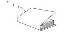
- FIG. 1 is a perspective view of a sample kit according to an embodiment of the present invention.
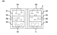
- FIG. 2 is a plan view schematically showing the internal structure of the sample kit of FIG.
- the sample kit 1 includes a storage body 2. As shown in FIG. 2, the storage body 2 includes storage portions S1 to S6.
- the storage units S1 to S5 are configured to store one or more electronic components 3A to 3E.
- the electronic components 3A to 3E are electronic components having different external shapes, terminal lengths, widths, arrangement pitches, positions, numbers, and the like.
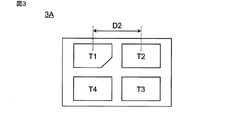
- the electronic component 3A is an electronic component including four terminals T1 to T4 (for example, a micro DC-DC converter manufactured by Murata Manufacturing Co., Ltd .: LXDC2HL, LXDC2HN, LXDC2MB series). As shown in FIG.
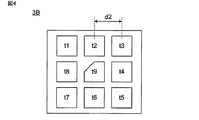
- the electronic component 3B is an electronic component having nine terminals t1 to t9 (for example, a micro DC-DC converter manufactured by Murata Manufacturing Co., Ltd .: LXDC2UR, LXDC2XQ, LXDC2SC series).
- the storage unit S6 is configured to store one or more conversion boards 4.
- the conversion board 4 is a board for fan-outing the terminals of the electronic components 3A to 3E to a land such as a prototype board 7 (see FIG. 7) and an evaluation board (see FIG. 8) described later.
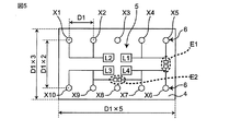
- the size of the conversion substrate 4 is larger than the electronic components 3A to 3E and smaller than the prototype substrate 7 and the evaluation board 8. As shown in FIG. 5, the conversion substrate 4 has an electronic component land pattern 5 and an input / output land pattern 6.
- the electronic component land pattern 5 is a land pattern for mounting any one of the plurality of electronic components 3A to 3E.
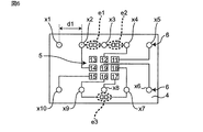
- the electronic component land pattern 5 is formed on both main surfaces of the conversion substrate 4 as shown in FIGS. 5 and 6.
- the electronic component land pattern 5 formed on one main surface of the conversion substrate 4 includes four electronic component lands L1 to L4, and an electronic component including four terminals T1 to T4 such as an electronic component 3A can be mounted. Is formed.
- the electronic component land pattern 5 formed on the other main surface of the conversion substrate 4 includes nine electronic component lands l1 to l9, and can mount an electronic component including nine terminals t1 to t9 such as the electronic component 3B. Is formed.
- An electronic component including four terminals, such as the electronic component 3A is an example of the first type of electronic component.
- An electronic component having nine terminals, such as the electronic component 3B is an example of a second type of electronic component.
- the input / output land pattern 6 is a land pattern for connection to a prototype board 7 as shown in FIG. 7 or an evaluation board 8 as shown in FIG.
- the input / output land pattern 6 is formed on both main surfaces of the conversion substrate 4.
- the input / output land pattern 6 formed on one main surface of the conversion substrate 4 includes a plurality of input / output lands X1 to X10.
- the input / output land pattern 6 formed on the other main surface of the conversion substrate 4 includes a plurality of input / output lands x1 to x10.
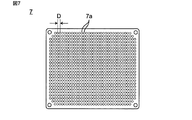
- the prototype substrate 7 is a universal substrate including a plurality of through holes 7a formed at intervals of the reference dimension D in the matrix direction (horizontal direction and vertical direction).
- the reference dimension D is, for example, 2.54 mm.
- the back surface of the universal substrate is plated so that it can be electrically soldered.
- a plurality of electronic components attached to the surface of the universal substrate are connected to each other on the back surface side of the universal substrate using a lead wire or the like.
- the evaluation board 8 is a board on which various components are mounted in order to evaluate the performance of the electronic components 3A to 3E, and includes a connection portion 8a to which the electronic components 3A to 3E are connected.
- the connection part 8a is comprised by the some through-hole, for example.
- the minimum dimension D1 (see FIG. 5) between the plurality of input / output lands X1 to X10 is designed to be larger than the maximum dimension D2 (see FIG. 3) between the plurality of terminals T1 to T4 included in the electronic component 3A. ing.
- the plurality of input / output lands X1 to X10 are arranged so that the distance between them is an integral multiple of a reference dimension larger than the dimension D1.
- the plurality of input / output lands X1 to X5 are arranged in the horizontal direction at intervals of the dimension D1, with the dimension D1 as a reference dimension.
- the plurality of input / output lands X6 to X10 are arranged in the horizontal direction at intervals of the dimension D1, with the dimension D1 as a reference dimension.
- the plurality of input / output lands X1 to X5 and the plurality of input / output lands X6 to X10 are arranged in the vertical direction at intervals of twice the dimension D1.
- the dimension D1 is designed to coincide with the reference dimension D that is the arrangement interval of the through holes 7a of the prototype substrate 7.
- FIG. 9 is a cross-sectional view of the electronic component mounting body 11 in which the electronic component 3A is connected to the prototype board 7 (or the evaluation board 8) cut along a plane passing through the input / output lands X1 and X10.
- the electronic component mounting body 11 includes the conductive pins 9 in the input / output lands X1 to X10 of the conversion board 4 and the plurality of through holes 7a of the prototype board 7 (or the connection portions 8a of the evaluation board 8). It inserts so that both ends may protrude, and it is comprised by soldering the both ends of the said conductive pin 9.
- the electronic component 3A may be mounted on the conversion board 4 after the conversion board 4 is connected to the prototype board 7 (or the evaluation board 8), or may be mounted on the conversion board 4 in advance.
- the minimum dimension d1 (see FIG. 6) between the plurality of input / output lands x1 to x10 is designed to be larger than the maximum dimension d2 (see FIG. 4) between the plurality of terminals t1 to t9 included in the electronic component 3B. ing.
- the plurality of input / output lands x1 to x10 are arranged so that the interval between them is an integral multiple of a reference dimension larger than the dimension d1.
- the plurality of input / output lands x1 to x5 are arranged in the horizontal direction at intervals of the dimension d1, with the dimension d1 as a reference dimension.
- the plurality of input / output lands x6 to x10 are arranged in the horizontal direction at intervals of the dimension d1, with the dimension d1 as a reference dimension.
- the plurality of input / output lands x1 to x5 and the plurality of input / output lands x6 to x10 are arranged in the vertical direction at intervals of twice the dimension d1.
- the dimension d1 is designed to coincide with the reference dimension D that is the arrangement interval of the through holes 7a of the prototype substrate 7.
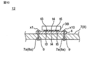
- FIG. 10 is a cross-sectional view of the electronic component mounting body 12 in which the electronic component 3B is connected to the prototype board 7 (or the evaluation board 8) cut along a plane passing through the input / output lands x1 and x10.
- the electronic component mounting body 12 has conductive pins 9 protruding at both ends thereof into input / output lands x1 to x10 of the conversion board 4 and a plurality of through holes 7a of the prototype board 7 (or connection portions 8a of the evaluation board 8). It inserts so that both ends of the conductive pin 9 may be soldered.
- the electronic component 3B may be mounted on the conversion board 4 after the conversion board 4 is connected to the prototype board 7 (or the evaluation board 8), or may be mounted on the conversion board 4 in advance.
- the outer shape of the conversion substrate 4 is formed in a rectangular shape as shown in FIGS.
- the length of each side of the outer shape of the conversion substrate 4 is designed to be an integral multiple of the reference dimension D1.
- the length of the short side (vertical) of the outer shape of the conversion substrate 4 is designed to be three times as long as D1.
- the length of the long side (lateral) of the outer shape of the conversion substrate 4 is designed to be five times as long as D1.
- an input capacitor may be attached to an area E1 surrounded by a broken line in FIG. 5 and an output capacitor may be attached to the area E2, as necessary.
- output capacitors may be attached to areas e1 and e2 surrounded by a broken line in FIG. 6 and input capacitors may be attached to the area e3 as necessary.
- the conversion board 4 having the electronic component land pattern 5 and the input / output land pattern 6 is stored in the storage body 2 of the sample kit 1 together with the plurality of electronic components 3A to 3E.
- a conversion substrate 4 it is possible to eliminate the need to change the design of the prototype substrate 7 or the evaluation board 8, and it is possible to more easily perform prototypes of electronic device systems and evaluation of electronic components. it can.
- the electronic component land pattern 5 is formed so that each of the plurality of electronic components 3A to 3E can be mounted.
- any of the plurality of electronic components 3A to 3E having different external shapes, terminal positions, and numbers can be mounted on one conversion board 4, making it easier to prototype electronic device systems and evaluate electronic components. Can be done.
- the electronic component land pattern 5 is formed on one main surface of the conversion substrate 4 so that the electronic component 3A (four terminals) can be mounted, and the other main surface of the conversion substrate 4 is mounted.
- the electronic component 3B (9 terminals) is formed so as to be mountable. Thereby, it is possible to deal with more electronic components with one conversion substrate 4.
- the minimum dimension D1, d1 between the plurality of input / output lands X1 to X10, x1 to x10 is larger than the maximum dimension D2, d2 between the plurality of terminals included in the electronic components 3A to 3E. Designed to be large. Thereby, even if the dimension between the terminals of the electronic components 3A to 3E is small, the dimension can be substantially enlarged by the conversion substrate 4. As a result, even if the electronic components 3A to 3E are downsized, by using the conversion substrate 4, it is possible to more easily prototype the system of the electronic device and evaluate the electronic component.
- the distance between the input / output lands X1 to X10 and x1 to x10 is designed to be an integral multiple of the reference dimension D of the universal board.
- the length of each side of the outer shape of the conversion substrate 4 is designed to be an integral multiple of the reference dimension D1.
- FIG. 11 is a flowchart showing a method for manufacturing the electronic component mounting body 11.
- one of the electronic components 3A to 3E is mounted on the electronic component land pattern 5 formed on the conversion substrate 4 (step S1).
- solder paste is printed on the electronic component lands L1 to L4 of the electronic component land pattern 5, and the terminals T1 to T4 of the electronic component 3A are placed on the electronic component lands L1 to L4.
- heat treatment such as reflow or hot press is performed to solder the electronic component lands L1 to L4 and the terminals T1 to T4 of the electronic component 3A.
- the prototype substrate 7 or the evaluation board 8 is connected to the input / output land pattern 6 formed on the conversion substrate 4 (step S2).
- the conductive pins 9 are inserted into the input / output lands x1 to x10 of the conversion substrate 4 and the plurality of through holes 7a of the prototype substrate 7 (or the connection portions 8a of the evaluation board 8) so that both ends protrude. Thereafter, both ends of the conductive pin 9 are soldered.
- the electronic component mounting body 11 can be manufactured.
- the prototype substrate 7 or the evaluation board 8 is connected to the input / output land pattern 6 of the conversion substrate 4 using the conductive pins 9, but the present invention is not limited to this.
- a prototype board 7 or an evaluation board 8 may be connected to the input / output land pattern 6 of the conversion board 4 using bolts 21 and socket pins 22. That is, by inserting the bolt 21 attached so as to penetrate the input / output lands X1 to X10 of the conversion board 4 into the insertion hole 22a of the socket pin 22 attached to the prototype board 7, A prototype substrate 7 or an evaluation board 8 may be connected to the pattern 6. In this case, since it is not necessary to use solder, it is possible to more easily perform trial manufacture of an electronic device system and evaluation of electronic components.
- the prototype substrate 7 or the evaluation board 8 may be connected to the input / output land pattern 6 of the conversion substrate 4 using lead wires. Even in this case, the same effect can be obtained.
- the electronic components 3A to 3E and the conversion board 4 are separately stored in the storage body 2, but the present invention is not limited to this.
- the electronic components 3A to 3E mounted in advance on the conversion board 4 may be stored in the storage body 2.
- the step of mounting the electronic components 3A to 3E on the conversion board 4 can be omitted, and the prototype of the electronic device system and the evaluation of the electronic components can be performed more easily.
- the electronic components 3A to 3E are electronic components having different external shapes, terminal lengths, widths, arrangement pitches, positions, numbers, etc., but the present invention is not limited to this. Not.
- the electronic components 3A to 3E may be the same component.
- the electronic component land pattern 5 and the input / output land pattern 6 are formed on both main surfaces of the conversion substrate 4, but the present invention is not limited to this.
- the electronic component land pattern 5 and the input / output land pattern 6 may be formed only on one main surface of the conversion substrate 4.
- the electronic component land pattern 5 is preferably formed so that a plurality of types of electronic components having different numbers of terminals can be mounted.
- the present invention can more easily perform trial manufacture of electronic device systems and evaluation of electronic components, it is useful for trial production of various electronic device systems and evaluation of electronic components.
Landscapes
- Engineering & Computer Science (AREA)
- Microelectronics & Electronic Packaging (AREA)
- General Physics & Mathematics (AREA)
- Physics & Mathematics (AREA)
- Mathematical Physics (AREA)
- Computational Mathematics (AREA)
- Mathematical Analysis (AREA)
- Mathematical Optimization (AREA)
- Algebra (AREA)
- Pure & Applied Mathematics (AREA)
- Business, Economics & Management (AREA)
- Educational Administration (AREA)
- Educational Technology (AREA)
- Theoretical Computer Science (AREA)
- Printing Elements For Providing Electric Connections Between Printed Circuits (AREA)
- Structure Of Printed Boards (AREA)
Abstract
電子機器のシステムの試作及び電子部品の評価をより容易に行うことができるサンプルキットを提供する。本発明に係るサンプルキット(1)は、複数の電子部品(3A~3E)と、複数の電子部品(3A~3E)のいずれか1つを実装するための電子部品用ランドパターン(5)、及び、試作用基板(7)又は評価ボード(8)に接続するための入出力用ランドパターン(6)を有する変換基板(4)と、複数の電子部品(3A~3E)と変換基板(4)とを収納する収納体(2)とを備える。
Description
本発明は、複数の電子部品を収納するサンプルキットに関する。
従来、電子機器のシステムを試作する際に、サンプルキットが利用されている。システムの設計者は、サンプルキットに収納された複数の電子部品の中から所望の電子部品を取り出し、当該電子部品をユニバーサル基板などの試作用基板に接続してシステムの試作を行っている。
また、従来、サンプルキットに収納された複数の電子部品の中から所望の電子部品を取り出し、当該電子部品を評価ボードに接続して、当該電子部品の性能を評価することも行われている。
近年、電子部品(例えば、受動部品、半導体部品、機構部品)は、小型化が進んでおり、端子間の間隔が狭くなっている。このため、これらの部品を実装できるように試作用基板又は評価ボードをその都度設計する必要があり、そのために時間及びコストがかかる。また、これらの部品を、例えばハンドワイヤを用いて試作用基板又は評価ボードに搭載及び配線することは難しくなっている。
従って、本発明の目的は、前記課題を解決することにあって、電子機器のシステムの試作及び電子部品の評価をより容易に行うことができるサンプルキット、変換基板、及び電子部品実装体の製造方法を提供することにある。
前記目的を達成するために、本発明に係るサンプルキットは、
複数の電子部品と、
前記複数の電子部品のいずれか1つを実装するための電子部品用ランドパターン、及び、試作用基板又は評価ボードに接続するための入出力用ランドパターンを有する変換基板と、
前記複数の電子部品と前記変換基板とを収納する収納体と、
を備える。
複数の電子部品と、
前記複数の電子部品のいずれか1つを実装するための電子部品用ランドパターン、及び、試作用基板又は評価ボードに接続するための入出力用ランドパターンを有する変換基板と、
前記複数の電子部品と前記変換基板とを収納する収納体と、
を備える。
また、本発明に係る変換基板は、
サンプルキットの収納体に収納された複数の電子部品のいずれか1つを試作用基板又は評価ボードに接続するための変換基板であって、
前記複数の電子部品のいずれか1つを実装するための電子部品用ランドパターンと、
前記試作用基板又は前記評価ボードに接続するための入出力用ランドパターンと、を有する。
サンプルキットの収納体に収納された複数の電子部品のいずれか1つを試作用基板又は評価ボードに接続するための変換基板であって、
前記複数の電子部品のいずれか1つを実装するための電子部品用ランドパターンと、
前記試作用基板又は前記評価ボードに接続するための入出力用ランドパターンと、を有する。
また、本発明に係る電子部品実装体の製造方法は、
電子部品が試作用基板又は評価ボードに接続された電子部品実装体の製造方法であって、
変換基板に形成された電子部品用ランドパターンに電子部品を実装する工程と、
前記変換基板に形成された入出力用ランドパターンに前記試作用基板又は前記評価ボードを接続する工程と、
を含む。
電子部品が試作用基板又は評価ボードに接続された電子部品実装体の製造方法であって、
変換基板に形成された電子部品用ランドパターンに電子部品を実装する工程と、
前記変換基板に形成された入出力用ランドパターンに前記試作用基板又は前記評価ボードを接続する工程と、
を含む。
本発明によれば、電子機器のシステムの試作をより容易に行うことができる。
(本発明の基礎となった知見)
本発明者らは、電子機器のシステムの試作をより容易に行うために鋭意検討した結果、以下の知見を得た。
本発明者らは、電子機器のシステムの試作をより容易に行うために鋭意検討した結果、以下の知見を得た。
従来においては、電子部品の端子間の間隔に対応するように試作用基板又は評価ボードを設計している。これに対して、本発明者らは、電子部品と試作用基板又は評価ボードとの間に、電子部品用ランドパターンと入出力用ランドパターンとを有する変換基板を設けることで、試作用基板又は評価ボードの設計を変更する必要性を無くすことができることを見出した。また、この変換基板をサンプルキットの収納体に複数の電子部品と共に収納することで、システム設計者の利便性を大幅に向上できることを見出した。
これらの点を踏まえて、本発明者らは、以下の発明に至った。
本発明の一態様に係るサンプルキットは、
複数の電子部品と、
前記複数の電子部品のいずれか1つを実装するための電子部品用ランドパターン、及び、試作用基板又は評価ボードに接続するための入出力用ランドパターンを有する変換基板と、
前記複数の電子部品と前記変換基板とを収納する収納体と、
を備える。
複数の電子部品と、
前記複数の電子部品のいずれか1つを実装するための電子部品用ランドパターン、及び、試作用基板又は評価ボードに接続するための入出力用ランドパターンを有する変換基板と、
前記複数の電子部品と前記変換基板とを収納する収納体と、
を備える。
この構成によれば、電子部品用ランドパターンと入出力用ランドパターンとを有する変換基板をサンプルキットの収納体に複数の電子部品と共に収納しているので、評価する電子部品に合わせて試作用基板又は評価ボードの設計を変更する必要性を無くすことができる。これにより、電子機器のシステムの試作及び電子部品の評価をより容易に行うことができる。
なお、前記電子部品用ランドパターンは、前記複数の電子部品のそれぞれを実装可能に形成されることが好ましい。この構成によれば、例えば、複数の電子部品の端子の形状がそれぞれ異なっていても、1つの変換基板でそれらの複数の電子部品のいずれも実装可能であるので、電子機器のシステムの試作及び電子部品の評価をより容易に行うことができる。
また、前記電子部品用ランドパターンは、前記複数の電子部品として、端子数が異なる複数種類の電子部品のそれぞれを実装可能に形成されることが好ましい。この構成によれば、複数の電子部品の端子数がそれぞれ異なっていても、1つの変換基板でそれらの複数の電子部品のいずれも実装可能であるので、電子機器のシステムの試作及び電子部品の評価をより容易に行うことができる。
また、前記電子部品用ランドパターンは、前記変換基板の一方の主面に第1種類の電子部品を実装可能に形成されるとともに、前記変換基板の他方の主面に第2種類の電子部品を実装可能に形成されることが好ましい。この構成によれば、変換基板の両主面に電子部品用ランドパターンが形成されているので、1つの変換基板でより多くの電子部品に対応することができる。
また、前記入出力用ランドパターンは、複数の入出力用ランドを備え、前記複数の入出力用ランド間の最小寸法は、前記電子部品が備える複数の端子間の最大寸法よりも大きいことが好ましい。この構成によれば、電子部品の端子間の寸法が小さくても、変換基板によって実質的に当該寸法を拡大することができる。これにより、電子部品が小型化しても、変換基板を用いることによって、電子機器のシステムの試作及び電子部品の評価をより容易に行うことができる。
また、前記試作用基板は、行列方向に基準寸法の間隔で形成された複数の貫通穴を備えるユニバーサル基板であり、前記入出力用ランドパターンは、互いの間隔が前記基準寸法の整数倍になるように配置された複数の入出力用ランドを備えることが好ましい。この構成によれば、一般に広く普及しているユニバーサル基板に変換基板を介して電子部品を実装することができるので、電子機器のシステムの試作及び電子部品の評価をより容易に行うことができる。
また、前記変換基板の外形は、矩形であり、前記変換基板の外形の各辺の長さは、前記基準寸法の整数倍の長さであることが好ましい。この構成によれば、例えば、ユニバーサル基板に複数の変換基板を敷き詰めるように配置することが可能になり、電子機器のシステムの試作及び電子部品の評価をより容易に行うことができる。
本発明の一態様に係る変換基板は、サンプルキットの収納体に収納された複数の電子部品のいずれか1つを試作用基板又は評価ボードに接続するための変換基板であって、
前記複数の電子部品のいずれか1つを実装するための電子部品用ランドパターンと、
前記試作用基板又は前記評価ボードに接続するための入出力用ランドパターンと、
を有する。
前記複数の電子部品のいずれか1つを実装するための電子部品用ランドパターンと、
前記試作用基板又は前記評価ボードに接続するための入出力用ランドパターンと、
を有する。
この構成によれば、電子部品用ランドパターンと入出力用ランドパターンとを有する変換基板を用いることで、試作用基板又は評価ボードの設計を変更する必要性を無くすことができる。これにより、電子機器のシステムの試作及び電子部品の評価をより容易に行うことができる。
本発明の一態様に係る電子部品実装体の製造方法は、
電子部品が試作用基板又は評価ボードに接続された電子部品実装体の製造方法であって、
変換基板に形成された電子部品用ランドパターンに電子部品を実装する工程と、
前記変換基板に形成された入出力用ランドパターンに前記試作用基板又は前記評価ボードを接続する工程と、
を含む。
電子部品が試作用基板又は評価ボードに接続された電子部品実装体の製造方法であって、
変換基板に形成された電子部品用ランドパターンに電子部品を実装する工程と、
前記変換基板に形成された入出力用ランドパターンに前記試作用基板又は前記評価ボードを接続する工程と、
を含む。
この方法によれば、電子部品用ランドパターンと入出力用ランドパターンとを有する変換基板を用いることで、試作用基板又は評価ボードの設計を変更する必要性を無くすことができる。これにより、電子機器のシステムの試作及び電子部品の評価をより容易に行うことができる。
以下、本発明の実施形態について、図面を参照しながら説明する。
《実施形態》
図1は、本発明の実施形態に係るサンプルキットの斜視図である。図2は、図1のサンプルキットの内部構造を模式的に示す平面図である。
図1は、本発明の実施形態に係るサンプルキットの斜視図である。図2は、図1のサンプルキットの内部構造を模式的に示す平面図である。
図1に示すように、本実施形態に係るサンプルキット1は、収納体2を備えている。収納体2は、図2に示すように、収納部S1~S6を備えている。
収納部S1~S5は、1以上の電子部品3A~3Eを収納するように構成されている。電子部品3A~3Eは、互いに外形形状や、端子の長さ、幅、配置ピッチ、位置、数等が異なる電子部品である。本実施形態において、電子部品3Aは、図3に示すように、4つの端子T1~T4を備える電子部品(例えば、村田製作所製マイクロDC-DCコンバータ:LXDC2HL、LXDC2HN、LXDC2MBシリーズ)である。電子部品3Bは、図4に示すように、9つの端子t1~t9を備える電子部品(例えば、村田製作所製マイクロDC-DCコンバータ:LXDC2UR、LXDC2XQ、LXDC2SCシリーズ)である。
収納部S6は、1以上の変換基板4を収納するように構成されている。変換基板4は、電子部品3A~3Eの端子を、後述する試作用基板7(図7参照)、評価ボード(図8参照)などのランドにファンアウトするための基板である。変換基板4のサイズは、電子部品3A~3Eよりも大きく、試作用基板7及び評価ボード8よりも小さい。変換基板4は、図5に示すように、電子部品用ランドパターン5と、入出力用ランドパターン6とを有している。
電子部品用ランドパターン5は、複数の電子部品3A~3Eのいずれか1つを実装するためのランドパターンである。本実施形態において、電子部品用ランドパターン5は、図5及び図6に示すように、変換基板4の両主面に形成されている。変換基板4の一方の主面に形成された電子部品用ランドパターン5は、4つの電子部品用ランドL1~L4を備え、電子部品3Aなどの4つの端子T1~T4を備える電子部品を実装可能に形成されている。変換基板4の他方の主面に形成された電子部品用ランドパターン5は、9つの電子部品用ランドl1~l9を備え、電子部品3Bなどの9つの端子t1~t9を備える電子部品を実装可能に形成されている。電子部品3Aなどの4つの端子を備える電子部品は、第1種類の電子部品の一例である。電子部品3Bなどの9つの端子を備える電子部品は、第2種類の電子部品の一例である。
入出力用ランドパターン6は、図7に示すような試作用基板7又は図8に示すような評価ボード8に接続するためのランドパターンである。本実施形態において、入出力用ランドパターン6は、変換基板4の両主面に形成されている。変換基板4の一方の主面に形成された入出力用ランドパターン6は、複数の入出力用ランドX1~X10を備えている。変換基板4の他方の主面に形成された入出力用ランドパターン6は、複数の入出力用ランドx1~x10を備えている。
本実施形態において、試作用基板7は、行列方向(横方向及び縦方向)に基準寸法Dの間隔で形成された複数の貫通穴7aを備えるユニバーサル基板である。基準寸法Dは、例えば、2.54mmである。ユニバーサル基板の裏面には、電気的にはんだ付けできるようにメッキ処理が施されている。ユニバーサル基板の表面に取り付けられた複数の電子部品同士は、ユニバーサル基板の裏面側でリード線などを用いて接続される。評価ボード8は、各電子部品3A~3Eの性能を評価するために各種部品が実装された基板であり、各電子部品3A~3Eが接続される接続部8aを備えている。接続部8aは、例えば、複数の貫通穴で構成されている。
複数の入出力用ランドX1~X10間の最小寸法D1(図5参照)は、電子部品3Aが備える複数の端子T1~T4間の最大寸法D2(図3参照)よりも大きくなるように設計されている。複数の入出力用ランドX1~X10は、互いの間隔が寸法D1よりも大きい基準寸法の整数倍になるように配置されている。本実施形態において、複数の入出力用ランドX1~X5は、寸法D1を基準寸法として、寸法D1の間隔で横方向に配置されている。複数の入出力用ランドX6~X10は、寸法D1を基準寸法として、寸法D1の間隔で横方向に配置されている。複数の入出力用ランドX1~X5と複数の入出力用ランドX6~X10とは、寸法D1の2倍の間隔で縦方向に配置されている。また、本実施形態において、寸法D1は、試作用基板7の貫通穴7aの配置間隔である基準寸法Dと一致するように設計されている。
図9は、電子部品3Aが試作用基板7(又は評価ボード8)に接続された電子部品実装体11を入出力用ランドX1,X10を通る面で切った断面図である。本実施形態において、電子部品実装体11は、変換基板4の入出力用ランドX1~X10及び試作用基板7の複数の貫通穴7a(又は評価ボード8の接続部8a)に導電性ピン9を両端部が突出するように挿入し、当該導電性ピン9の両端部をはんだ付けすることにより構成されている。電子部品3Aは、変換基板4を試作用基板7(又は評価ボード8)に接続した後、変換基板4に実装されてもよいし、変換基板4に予め実装されてもよい。
複数の入出力用ランドx1~x10間の最小寸法d1(図6参照)は、電子部品3Bが備える複数の端子t1~t9間の最大寸法d2(図4参照)よりも大きくなるように設計されている。複数の入出力用ランドx1~x10は、互いの間隔が寸法d1よりも大きい基準寸法の整数倍になるように配置されている。本実施形態において、複数の入出力用ランドx1~x5は、寸法d1を基準寸法として、寸法d1の間隔で横方向に配置されている。複数の入出力用ランドx6~x10は、寸法d1を基準寸法として、寸法d1の間隔で横方向に配置されている。複数の入出力用ランドx1~x5と複数の入出力用ランドx6~x10とは、寸法d1の2倍の間隔で縦方向に配置されている。また、本実施形態において、寸法d1は、試作用基板7の貫通穴7aの配置間隔である基準寸法Dと一致するように設計されている。
図10は、電子部品3Bが試作用基板7(又は評価ボード8)に接続された電子部品実装体12を入出力用ランドx1,x10を通る面で切った断面図である。電子部品実装体12は、変換基板4の入出力用ランドx1~x10及び試作用基板7の複数の貫通穴7a(又は評価ボード8の接続部8a)に導電性ピン9を両端部が突出するように挿入し、当該導電性ピン9の両端部をはんだ付けすることにより構成されている。電子部品3Bは、変換基板4を試作用基板7(又は評価ボード8)に接続した後、変換基板4に実装されてもよいし、変換基板4に予め実装されてもよい。
また、本実施形態において、変換基板4の外形は、図5及び図6に示すように、矩形に形成されている。変換基板4の外形の各辺の長さは、基準寸法D1の整数倍の長さに設計されている。例えば、変換基板4の外形の短辺(縦)の長さは、D1の3倍の長さに設計されている。変換基板4の外形の長辺(横)の長さは、D1の5倍の長さに設計されている。
なお、変換基板4の一方の主面には、必要に応じて、図5において破線で囲まれたエリアE1に入力コンデンサが取り付けられ、エリアE2に出力コンデンサが取り付けられてもよい。また、変換基板4の他方の主面には、必要に応じて、図6において破線で囲まれたエリアe1,e2に出力コンデンサが取り付けられ、エリアe3に入力コンデンサが取り付けられてもよい。
本実施形態によれば、電子部品用ランドパターン5と入出力用ランドパターン6とを有する変換基板4をサンプルキット1の収納体2に複数の電子部品3A~3Eと共に収納している。このような変換基板4を用いることにより、試作用基板7又は評価ボード8の設計を変更する必要性を無くすことができ、電子機器のシステムの試作及び電子部品の評価をより容易に行うことができる。
また、本実施形態によれば、電子部品用ランドパターン5が、複数の電子部品3A~3Eのそれぞれを実装可能に形成されている。これにより、外形形状や端子の位置、数が異なる複数の電子部品3A~3Eのいずれも、1つの変換基板4で実装可能であるので、電子機器のシステムの試作及び電子部品の評価をより容易に行うことができる。
また、本実施形態によれば、電子部品用ランドパターン5が、変換基板4の一方の主面に電子部品3A(4端子)を実装可能に形成されるとともに、変換基板4の他方の主面に電子部品3B(9端子)を実装可能に形成されている。これにより、1つの変換基板4でより多くの電子部品に対応することができる。
また、本実施形態によれば、複数の入出力用ランドX1~X10、x1~x10間の最小寸法D1,d1が、電子部品3A~3Eが備える複数の端子間の最大寸法D2,d2よりも大きくなるように設計されている。これにより、電子部品3A~3Eの端子間の寸法が小さくても、変換基板4によって実質的に当該寸法を拡大することができる。これにより、電子部品3A~3Eが小型化しても、変換基板4を用いることによって、電子機器のシステムの試作及び電子部品の評価をより容易に行うことができる。
また、本実施形態によれば、入出力用ランドX1~X10,x1~x10の互いの間隔が、ユニバーサル基板の基準寸法Dの整数倍になるように設計されている。これにより、一般に広く普及しているユニバーサル基板に変換基板4を介して電子部品3A~3Eを実装することができるので、電子機器のシステムの試作及び電子部品の評価をより容易に行うことができる。
また、本実施形態によれば、変換基板4の外形の各辺の長さが、基準寸法D1の整数倍の長さに設計されている。これにより、例えば、ユニバーサル基板に複数の変換基板4を敷き詰めるように配置することが可能になり、スペースを有効に活用して、電子機器のシステムの試作及び電子部品の評価をより容易に行うことができる。
次に、電子部品実装体11の製造方法の一例について説明する。図11は、電子部品実装体11の製造方法を示すフローチャートである。
まず、変換基板4に形成された電子部品用ランドパターン5に電子部品3A~3Eのいずれか1つを実装する(ステップS1)。例えば、電子部品用ランドパターン5の電子部品用ランドL1~L4にはんだペーストを印刷し、当該電子部品用ランドL1~L4に電子部品3Aの端子T1~T4を載置する。その後、リフローやホットプレスなどの熱処理を行うことで、電子部品用ランドL1~L4と電子部品3Aの端子T1~T4とをはんだ付けする。
次いで、変換基板4に形成された入出力用ランドパターン6に試作用基板7又は評価ボード8を接続する(ステップS2)。例えば、変換基板4の入出力用ランドx1~x10及び試作用基板7の複数の貫通穴7a(又は評価ボード8の接続部8a)に導電性ピン9を両端部が突出するように挿入する。その後、導電性ピン9の両端部をはんだ付けする。
以上のようにして、電子部品実装体11を製造することができる。
なお、本実施形態では、導電性ピン9を用いて変換基板4の入出力用ランドパターン6に試作用基板7又は評価ボード8を接続するようにしたが、本発明はこれに限定されない。例えば、図12に示すように、ボルト21及びソケットピン22を用いて変換基板4の入出力用ランドパターン6に試作用基板7又は評価ボード8を接続するようにしてもよい。すなわち、変換基板4の入出力用ランドX1~X10を貫通するように取り付けられたボルト21を、試作用基板7に取り付けられたソケットピン22の挿入穴22aに挿入することで、入出力用ランドパターン6に試作用基板7又は評価ボード8を接続してもよい。この場合、はんだを用いる必要がないので、電子機器のシステムの試作及び電子部品の評価をより容易に行うことができる。
また、導電性ピン9に代えて、リード線を用いて変換基板4の入出力用ランドパターン6に試作用基板7又は評価ボード8を接続するようにしてもよい。この場合でも、同様の効果を得ることができる。
また、本実施形態では、電子部品3A~3Eと変換基板4とを別々に収納体2に収納するようにしたが、本発明はこれに限定されない。例えば、各電子部品3A~3Eを変換基板4に予め実装したものを収納体2に収納するようにしてもよい。この場合、各電子部品3A~3Eを変換基板4に実装する工程を省略することができ、電子機器のシステムの試作及び電子部品の評価をより容易に行うことができる。
また、本実施形態では、電子部品3A~3Eは、互いに外形形状や、端子の長さ、幅、配置ピッチ、位置、数等が異なる電子部品であるものとしたが、本発明はこれに限定されない。例えば、電子部品3A~3Eは、同じ部品であってもよい。
また、本実施形態では、電子部品用ランドパターン5及び入出力用ランドパターン6は、変換基板4の両主面に形成されるものとしたが、本発明はこれに限定されない。例えば、電子部品用ランドパターン5及び入出力用ランドパターン6は、それぞれ、変換基板4の一方の主面のみに形成されてもよい。また、この場合、電子部品用ランドパターン5は、端子数が異なる複数種類の電子部品を実装可能に形成されることが好ましい。
本発明は、添付図面を参照しながら好ましい実施の形態に関連して充分に記載されているが、この技術に熟練した人々にとっては種々の変形や修正は明白である。そのような変形や修正は、添付した請求の範囲による本発明の範囲から外れない限りにおいて、その中に含まれると理解されるべきである。
本発明は、電子機器のシステムの試作及び電子部品の評価をより容易に行うことができるので、様々な電子機器のシステムの試作及び電子部品の評価の際に有用である。
1 サンプルキット
2 収納体
3A~3E 電子部品
4 変換基板
5 電子部品用ランドパターン
6 入出力用ランドパターン
7 試作用基板
7a 貫通穴
8 評価ボード
8a 接続部
9 導電性ピン
11,12 電子部品実装体
21 ボルト
22 ソケットピン
22a 挿入穴
T1~T4,t1~t9 端子
L1~L4,l1~l9 電子部品用ランド
X1~X10,x1~x10 入出力用ランド
E1,E2,e1~e3 エリア
2 収納体
3A~3E 電子部品
4 変換基板
5 電子部品用ランドパターン
6 入出力用ランドパターン
7 試作用基板
7a 貫通穴
8 評価ボード
8a 接続部
9 導電性ピン
11,12 電子部品実装体
21 ボルト
22 ソケットピン
22a 挿入穴
T1~T4,t1~t9 端子
L1~L4,l1~l9 電子部品用ランド
X1~X10,x1~x10 入出力用ランド
E1,E2,e1~e3 エリア
Claims (21)
- 複数の電子部品と、
前記複数の電子部品のいずれか1つを実装するための電子部品用ランドパターン、及び、試作用基板又は評価ボードに接続するための入出力用ランドパターンを有する変換基板と、
前記複数の電子部品と前記変換基板とを収納する収納体と、
を備える、サンプルキット。 - 前記電子部品用ランドパターンは、前記複数の電子部品のそれぞれを実装可能に形成されている、請求項1に記載のサンプルキット。
- 前記電子部品用ランドパターンは、前記複数の電子部品として、端子数が異なる複数種類の電子部品のそれぞれを実装可能に形成されている、請求項2に記載のサンプルキット。
- 前記電子部品用ランドパターンは、前記変換基板の一方の主面に第1種類の電子部品を実装可能に形成されるとともに、前記変換基板の他方の主面に第2種類の電子部品を実装可能に形成されている、請求項3に記載のサンプルキット。
- 前記入出力用ランドパターンは、複数の入出力用ランドを備え、
前記複数の入出力用ランド間の最小寸法は、前記電子部品が備える複数の端子間の最大寸法よりも大きい、請求項1~4のいずれか1つに記載のサンプルキット。 - 前記試作用基板は、行列方向に基準寸法の間隔で形成された複数の貫通穴を備えるユニバーサル基板であり、
前記入出力用ランドパターンは、互いの間隔が前記基準寸法の整数倍になるように配置された複数の入出力用ランドを備える、請求項1~5のいずれか1つに記載のサンプルキット。 - 前記変換基板の外形は、矩形であり、
前記変換基板の外形の各辺の長さは、前記基準寸法の整数倍の長さである、
請求項6に記載のサンプルキット。 - サンプルキットの収納体に収納された複数の電子部品のいずれか1つを試作用基板又は評価ボードに接続するための変換基板であって、
前記複数の電子部品のいずれか1つを実装するための電子部品用ランドパターンと、
前記試作用基板又は前記評価ボードに接続するための入出力用ランドパターンと、
を有する、変換基板。 - 前記電子部品用ランドパターンは、前記複数の電子部品のそれぞれを実装可能に形成されている、請求項8に記載の変換基板。
- 前記電子部品用ランドパターンは、前記複数の電子部品として、端子数が異なる複数種類の電子部品のそれぞれを実装可能に形成されている、請求項9に記載の変換基板。
- 前記電子部品用ランドパターンは、前記変換基板の一方の主面に第1種類の電子部品を実装可能に形成されるとともに、前記変換基板の他方の主面に第2種類の電子部品を実装可能に形成されている、請求項10に記載の変換基板。
- 前記入出力用ランドパターンは、複数の入出力用ランドを備え、
前記複数の入出力用ランド間の最小寸法は、前記電子部品が備える複数の端子間の最大寸法よりも大きい、請求項8~11のいずれか1つに記載の変換基板。 - 前記試作用基板は、行列方向に基準寸法の間隔で形成された複数の貫通穴を備えるユニバーサル基板であり、
前記入出力用ランドパターンは、互いの間隔が前記基準寸法の整数倍になるように配置された複数の入出力用ランドを備える、請求項8~12のいずれか1つに記載の変換基板。 - 前記変換基板の外形は、矩形であり、
前記変換基板の外形の各辺の長さは、前記基準寸法の整数倍の長さである、
請求項13に記載の変換基板。 - 電子部品が試作用基板又は評価ボードに接続された電子部品実装体の製造方法であって、
変換基板に形成された電子部品用ランドパターンに電子部品を実装する工程と、
前記変換基板に形成された入出力用ランドパターンに前記試作用基板又は前記評価ボードを接続する工程と、
を含む、電子部品実装体の製造方法。 - 前記電子部品は、サンプルキットの収納体に収納された複数の電子部品のいずれか1つであり、
前記電子部品用ランドパターンは、前記複数の電子部品のそれぞれを実装可能に形成されている、請求項15に記載の電子部品実装体の製造方法。 - 前記電子部品用ランドパターンは、前記複数の電子部品として、端子数が異なる複数種類の電子部品のそれぞれを実装可能に形成されている、請求項16に記載の電子部品実装体の製造方法。
- 前記電子部品用ランドパターンは、前記変換基板の一方の主面に第1種類の電子部品を実装可能に形成されるとともに、前記変換基板の他方の主面に第2種類の電子部品を実装可能に形成されている、請求項17に記載の電子部品実装体の製造方法。
- 前記入出力用ランドパターンは、複数の入出力用ランドを備え、
前記複数の入出力用ランド間の最小寸法は、前記電子部品が備える複数の端子間の最大寸法よりも大きい、請求項15~18のいずれか1つに記載の電子部品実装体の製造方法。 - 前記試作用基板は、行列方向に基準寸法の間隔で形成された複数の貫通穴を備えるユニバーサル基板であり、
前記入出力用ランドパターンは、互いの間隔が前記基準寸法の整数倍になるように配置された複数の入出力用ランドを備える、請求項15~19のいずれか1つに記載の電子部品実装体の製造方法。 - 前記変換基板の外形は、矩形であり、
前記変換基板の外形の各辺の長さは、前記基準寸法の整数倍の長さである、
請求項20に記載の電子部品実装体の製造方法。
Applications Claiming Priority (2)
| Application Number | Priority Date | Filing Date | Title |
|---|---|---|---|
| JP2016-121159 | 2016-06-17 | ||
| JP2016121159A JP2019165032A (ja) | 2016-06-17 | 2016-06-17 | サンプルキット、変換基板、及び電子部品実装体の製造方法 |
Publications (1)
| Publication Number | Publication Date |
|---|---|
| WO2017217211A1 true WO2017217211A1 (ja) | 2017-12-21 |
Family
ID=60663616
Family Applications (1)
| Application Number | Title | Priority Date | Filing Date |
|---|---|---|---|
| PCT/JP2017/019533 Ceased WO2017217211A1 (ja) | 2016-06-17 | 2017-05-25 | サンプルキット、変換基板、及び電子部品実装体の製造方法 |
Country Status (2)
| Country | Link |
|---|---|
| JP (1) | JP2019165032A (ja) |
| WO (1) | WO2017217211A1 (ja) |
Citations (4)
| Publication number | Priority date | Publication date | Assignee | Title |
|---|---|---|---|---|
| JPS62168679U (ja) * | 1986-04-14 | 1987-10-26 | ||
| JPS63191642U (ja) * | 1987-05-29 | 1988-12-09 | ||
| JPH0596864U (ja) * | 1992-06-01 | 1993-12-27 | 沖電線株式会社 | Smt対応回路実験キット |
| US20100304580A1 (en) * | 2009-05-26 | 2010-12-02 | Thomas Baycura | Electrical component interface |
-
2016
- 2016-06-17 JP JP2016121159A patent/JP2019165032A/ja active Pending
-
2017
- 2017-05-25 WO PCT/JP2017/019533 patent/WO2017217211A1/ja not_active Ceased
Patent Citations (4)
| Publication number | Priority date | Publication date | Assignee | Title |
|---|---|---|---|---|
| JPS62168679U (ja) * | 1986-04-14 | 1987-10-26 | ||
| JPS63191642U (ja) * | 1987-05-29 | 1988-12-09 | ||
| JPH0596864U (ja) * | 1992-06-01 | 1993-12-27 | 沖電線株式会社 | Smt対応回路実験キット |
| US20100304580A1 (en) * | 2009-05-26 | 2010-12-02 | Thomas Baycura | Electrical component interface |
Also Published As
| Publication number | Publication date |
|---|---|
| JP2019165032A (ja) | 2019-09-26 |
Similar Documents
| Publication | Publication Date | Title |
|---|---|---|
| EP2627160A1 (en) | Circuit board system | |
| US10869382B2 (en) | Interposer and electronic apparatus | |
| US20130203274A1 (en) | Circuit board system | |
| US7203074B1 (en) | Electronic circuit building block | |
| KR100355753B1 (ko) | 보드용 커넥터 | |
| JP7257445B2 (ja) | 基板モジュール | |
| JP2014110224A (ja) | 保持部材及びコネクタ | |
| WO2017217211A1 (ja) | サンプルキット、変換基板、及び電子部品実装体の製造方法 | |
| US6381120B2 (en) | Mounting arrangement for multilayer electronic part | |
| JPH10135622A (ja) | 高周波機器の製造方法 | |
| JP2018032779A (ja) | 基板セット及び基板セットの製造方法 | |
| JP2016025690A (ja) | 電子モジュール | |
| JP2008034672A (ja) | チップ部品の実装方法および電子モジュール | |
| JP5874552B2 (ja) | 接合部材 | |
| JP2012104627A (ja) | プリント基板 | |
| JP3008887U (ja) | Icピッチ変換基板 | |
| JP2010114738A (ja) | プリント基板実装部品 | |
| JP4985852B2 (ja) | 実装型電子回路モジュール | |
| US20030214796A1 (en) | High frequency module mounting structure in which solder is prevented from peeling | |
| JP2011044519A (ja) | 電子部品実装構造 | |
| JP7301699B2 (ja) | ソケット | |
| JP6738688B2 (ja) | 基板セット及び固定用サブ基板 | |
| JP2006303248A (ja) | 三次元基板間接続部品、電子機器及び電子機器の製造方法 | |
| JPH0427195Y2 (ja) | ||
| JP2006303252A (ja) | 回路基板 |
Legal Events
| Date | Code | Title | Description |
|---|---|---|---|
| 121 | Ep: the epo has been informed by wipo that ep was designated in this application |
Ref document number: 17813113 Country of ref document: EP Kind code of ref document: A1 |
|
| NENP | Non-entry into the national phase |
Ref country code: DE |
|
| 122 | Ep: pct application non-entry in european phase |
Ref document number: 17813113 Country of ref document: EP Kind code of ref document: A1 |
|
| NENP | Non-entry into the national phase |
Ref country code: JP |