WO2017208802A1 - Semiconductor device - Google Patents
Semiconductor device Download PDFInfo
- Publication number
- WO2017208802A1 WO2017208802A1 PCT/JP2017/018308 JP2017018308W WO2017208802A1 WO 2017208802 A1 WO2017208802 A1 WO 2017208802A1 JP 2017018308 W JP2017018308 W JP 2017018308W WO 2017208802 A1 WO2017208802 A1 WO 2017208802A1
- Authority
- WO
- WIPO (PCT)
- Prior art keywords
- conductor layer
- semiconductor device
- heat
- electronic component
- conductor
- Prior art date
Links
Images


Classifications
-
- H—ELECTRICITY
- H01—ELECTRIC ELEMENTS
- H01L—SEMICONDUCTOR DEVICES NOT COVERED BY CLASS H10
- H01L23/00—Details of semiconductor or other solid state devices
- H01L23/12—Mountings, e.g. non-detachable insulating substrates
-
- H—ELECTRICITY
- H01—ELECTRIC ELEMENTS
- H01L—SEMICONDUCTOR DEVICES NOT COVERED BY CLASS H10
- H01L23/00—Details of semiconductor or other solid state devices
- H01L23/34—Arrangements for cooling, heating, ventilating or temperature compensation ; Temperature sensing arrangements
- H01L23/36—Selection of materials, or shaping, to facilitate cooling or heating, e.g. heatsinks
-
- H—ELECTRICITY
- H05—ELECTRIC TECHNIQUES NOT OTHERWISE PROVIDED FOR
- H05K—PRINTED CIRCUITS; CASINGS OR CONSTRUCTIONAL DETAILS OF ELECTRIC APPARATUS; MANUFACTURE OF ASSEMBLAGES OF ELECTRICAL COMPONENTS
- H05K1/00—Printed circuits
- H05K1/02—Details
-
- H—ELECTRICITY
- H05—ELECTRIC TECHNIQUES NOT OTHERWISE PROVIDED FOR
- H05K—PRINTED CIRCUITS; CASINGS OR CONSTRUCTIONAL DETAILS OF ELECTRIC APPARATUS; MANUFACTURE OF ASSEMBLAGES OF ELECTRICAL COMPONENTS
- H05K7/00—Constructional details common to different types of electric apparatus
- H05K7/20—Modifications to facilitate cooling, ventilating, or heating
-
- H—ELECTRICITY
- H01—ELECTRIC ELEMENTS
- H01L—SEMICONDUCTOR DEVICES NOT COVERED BY CLASS H10
- H01L2224/00—Indexing scheme for arrangements for connecting or disconnecting semiconductor or solid-state bodies and methods related thereto as covered by H01L24/00
- H01L2224/01—Means for bonding being attached to, or being formed on, the surface to be connected, e.g. chip-to-package, die-attach, "first-level" interconnects; Manufacturing methods related thereto
- H01L2224/26—Layer connectors, e.g. plate connectors, solder or adhesive layers; Manufacturing methods related thereto
- H01L2224/31—Structure, shape, material or disposition of the layer connectors after the connecting process
- H01L2224/32—Structure, shape, material or disposition of the layer connectors after the connecting process of an individual layer connector
- H01L2224/321—Disposition
- H01L2224/32151—Disposition the layer connector connecting between a semiconductor or solid-state body and an item not being a semiconductor or solid-state body, e.g. chip-to-substrate, chip-to-passive
- H01L2224/32221—Disposition the layer connector connecting between a semiconductor or solid-state body and an item not being a semiconductor or solid-state body, e.g. chip-to-substrate, chip-to-passive the body and the item being stacked
- H01L2224/32225—Disposition the layer connector connecting between a semiconductor or solid-state body and an item not being a semiconductor or solid-state body, e.g. chip-to-substrate, chip-to-passive the body and the item being stacked the item being non-metallic, e.g. insulating substrate with or without metallisation
Definitions
- the present invention relates to a semiconductor device, and more particularly to a semiconductor device that radiates heat generated from electronic components on a printed board through the printed board.
- Patent Document 1 Japanese Patent Application Laid-Open No. 6-77679
- Patent Document 2 Japanese Patent Application Laid-Open No. 11-34592
- an electronic component is joined above a printed circuit board, and a heat sink is fixed below.
- the printed circuit board has a heat conduction path formed so as to penetrate from one main surface to the other main surface. With this heat conduction path, heat generated from the electronic component is transmitted to the heat sink via the heat conduction path, and can be radiated from the heat sink to the outside.
- the present invention has been made in view of the above problems, and its purpose is to enable heat conduction from an electronic component to a radiator over a wide range centering on the electronic component, and to dissipate heat generated by the electronic component. It is an object to provide a semiconductor device capable of improving the above.
- the semiconductor device of the present invention includes a printed circuit board, an electronic component thereon, and a radiator below it.
- the printed circuit board includes an insulating layer and a conductor layer.
- Each of the plurality of conductor layers includes a plurality of first conductor layers electrically connected to the electronic component, and a plurality of first conductor layers spaced apart from each other and electrically insulated.
- a second conductor layer A plurality of first conductor layers connected to each of the first through-holes extending from one main surface of the printed circuit board to the other main surface; and connected to each of the plurality of second conductive layers; A second penetrating portion extending from one main surface to the other main surface.
- the first conductor layer and the second conductor layer at least partially overlap each other in a planar manner, or are spaced apart from each other in the direction along one main surface.
- the present invention there is a path for radiating heat over a wide range including not only the lower part of the electronic part but also the area outside the electronic part. Since the range of the heat dissipation path is widened, the thermal resistance in the region from the electronic component to the radiator can be reduced, and a semiconductor device having high heat dissipation performance from the electronic component to the radiator can be provided.
- FIG. 1 is a schematic cross-sectional view showing a configuration of a semiconductor device as a first example of Embodiment 1.
- FIG. 3 is a schematic cross-sectional view showing a configuration of a semiconductor device as a second example of the first embodiment.
- FIG. 4 is a schematic cross-sectional view showing a configuration of a semiconductor device as a third example of the first embodiment.
- FIG. 6 is a schematic cross sectional view showing the configuration of a semiconductor device as a fourth example of the first embodiment.
- FIG. 6 is a schematic cross-sectional view showing a configuration of a semiconductor device as a fifth example of the first embodiment.
- FIG. 6 is a schematic cross-sectional view showing a configuration of a semiconductor device as a sixth example of the first embodiment.
- FIG. FIG. 6 is a schematic cross-sectional view showing a configuration of a semiconductor device as a first example of the second embodiment.
- FIG. 6 is a schematic cross-sectional view showing a configuration of a semiconductor device as a second example of the second embodiment.
- FIG. 6 is a schematic cross-sectional view showing a configuration of a semiconductor device as a third example of the second embodiment.
- FIG. 6 is a schematic cross-sectional view showing a configuration of a semiconductor device as a fourth example of the second embodiment.
- FIG. 10 is a schematic cross-sectional view showing a configuration of a semiconductor device as a first example of the third embodiment. 12 is a schematic cross-sectional view showing a configuration of a semiconductor device as a second example of the third embodiment.
- FIG. FIG. 10 is a schematic cross-sectional view showing a part of the configuration of a semiconductor device according to a fourth embodiment and a heat transfer mode from an electronic component to a heat dissipation housing in the semiconductor device.
- FIG. 16 is a schematic enlarged perspective view of a region XVI surrounded by a dotted line in FIG. 15.
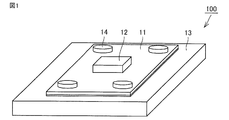
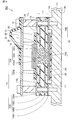
- FIG. FIG. 1 shows the appearance of the whole or a part of the semiconductor device of this embodiment. That is, when FIG. 1 is a part of a semiconductor device, FIG. 1 shows a mode in which only a part of the whole semiconductor device is cut out.
- semiconductor device 100 of the present embodiment is used for a power conversion device mounted on, for example, power electronics equipment.
- the semiconductor device 100 mainly includes a printed circuit board 11, an electronic component 12, a heat radiating housing 13, and screws 14.
- the printed circuit board 11 is a flat plate member having a rectangular shape in plan view, for example, which forms the foundation of the entire semiconductor device 100.
- a plurality of wirings that is, conductor layers, which will be described later, are formed on the printed circuit board 11.
- the plurality of conductor layers electrically connect the electronic component 12 and other peripheral circuit components not shown.
- the electronic component 12 is bonded to one main surface side of the printed circuit board 11, that is, the upper side in FIG.
- the electronic component 12 is a package in which a semiconductor chip including a MOSFET (Metal Oxide Semiconductor Field Effect Transistor), an IGBT (Insulated Gate Bipolar Transistor), or a diode is sealed with a resin. Since this semiconductor chip controls high power, the amount of heat generated by the electronic component 12 during operation of the semiconductor device 100 is as large as several watts to several tens of watts. For this reason, when the semiconductor device 100 is operated, a structure for radiating heat from the semiconductor device 100 by water cooling or air cooling is required.
- MOSFET Metal Oxide Semiconductor Field Effect Transistor
- IGBT Insulated Gate Bipolar Transistor
- the heat radiating housing 13 is a member as a heat radiator fixed to the other main surface side opposite to one main surface of the printed circuit board 11, that is, the lower side in FIG.
- the heat dissipating housing 13 is kept cooled to a certain temperature or lower by a device such as air cooling or water cooling (not shown) separately installed in the semiconductor device 100.
- the heat radiating housing 13 may be a heat radiating device such as a heat sink or a heat pipe instead of the housing.
- the radiator is assumed to be the heat radiating housing 13.
- the screw 14 is used as a fixing member that fixes the printed circuit board 11 so as to contact the heat radiating housing 13. Since the fixing member only needs to fix the printed circuit board 11 and the heat radiating housing 13, the connecting member is not limited to the screw 14, and other connecting members such as rivets may be used instead. Further, in FIG. 1, the screw 14 is disposed in a region that is generally adjacent to the four corners of the printed circuit board 11 in plan view. However, the number of screws 14 is not limited to four, and may be any number as long as the heat dissipating housing 13 can be fixed to the printed board 11 by fastening.
- heat generated in the electronic component 12 is conducted to the heat radiating housing 13 through the printed circuit board 11, and the heat radiating housing.
- the heat can be radiated from 13 to the outside of the semiconductor device 100.
- printed circuit board 11 includes one main surface 11a and the other main surface 11b on the opposite side. Have.
- the printed board 11 has a configuration including an insulating layer 11 ⁇ / b> C and a plurality of conductor layers 15.
- the insulating layer 11 ⁇ / b> C is a member that forms the main body of the printed circuit board 11.
- the insulating layer 11C is made of, for example, glass fiber and an epoxy resin, but is not limited thereto, and may be made of, for example, an aramid resin and an epoxy resin. Alternatively, the insulating layer 11C may be formed of a ceramic material.
- the conductor layer 15 extends along the main surface of the insulating layer 11C, that is, along one main surface 11a and the other main surface 11b of the printed board 11.
- a plurality of conductor layers 15 are laminated through a part of the insulating layer 11C from the electronic component 12 side, that is, the upper side of the printed board 11 to the heat radiating housing 13 side, that is, the lower side of the printed board 11. That is, a part of the insulating layer 11 ⁇ / b> C is sandwiched between one conductor layer 15 among the plurality of conductor layers 15 stacked and another conductor layer 15 adjacent thereto.
- the conductor layer 15 is laminated in four layers at intervals in the vertical direction of the figure.
- the four conductor layers 15 are laminated between the first conductor layer 15A and a plurality of first conductor layers 15A electrically connected to the electronic component 12 and the first conductor layer 15A in the left-right direction in the figure. And a plurality of, that is, four second conductor layers 15B, which are electrically insulated (for example, via the insulating layer 11C) and spaced apart from each other.
- the first conductor layer 15A and the second conductor layer 15B both extend along one main surface 11a and the other main surface 11b of the printed circuit board 11. Since the electronic component 12 is bonded to a relatively central portion of the printed circuit board 11 in a plan view, the first conductor layer 15A electrically connected to the electronic component 12 is formed on the relatively central portion of the printed circuit board 11.
- the second conductor layer 15B disposed between the first conductor layer 15A and the first conductor layer 15A via the insulating layer 11C is not electrically connected to the first conductor layer 15A. And is arranged in a relatively outer portion of the printed circuit board 11.
- the first conductor layer 15A has a first conductor layer 15A1, a first conductor layer 15A2, and a first conductor layer from the lower layer (radiation housing 13 side) to the upper layer (electronic component 12 side) in the figure. 15A3 and the first conductor layer 15A4 are stacked in this order.
- the second conductor layer 15B extends from the lower layer (heat dissipating housing 13 side) to the upper layer (electronic component 12 side) in the figure, the second conductor layer 15B1, the second conductor layer 15B2, and the second conductor.
- the layer 15B3 and the second conductor layer 15B4 are stacked in this order.
- the first conductor layer 15A1 and the second conductor layer 15B1 are formed as the same layer.
- each of the first conductor layer 15A2 and the second conductor layer 15B2, the first conductor layer 15A3 and the second conductor layer 15B3, and the first conductor layer 15A4 and the second conductor layer 15B4 are also formed as the same layer.
- the first conductor layer 15A and the second conductor layer 15B arranged as the same layer are arranged at a distance from each other in the horizontal direction of the drawing along the one main surface 11a.
- the distance between the first conductor layer 15A2 (15A3) and the second conductor layer 15B2 (15B3), which are the same layer, varies depending on the voltage handled by the semiconductor device 101, but is, for example, 0.4 mm or more.
- the first conductor layer 15A1 and the second conductor layer 15B1 are formed on the other main surface 11b of the printed circuit board 11.
- the first conductor layers 15A2 and 15A3 and the second conductor layers 15B2 and 15B3 are disposed inside the printed board 11 so as to be buried in the insulating layer 11C while maintaining a distance from the other conductor layers.
- the first conductor layer 15A4 and the second conductor layer 15B4 are formed on one main surface 11a of the printed board 11.
- the first conductor layers 15 ⁇ / b> A stacked on each other have one or the other main surfaces 11 a and 11 b based on the distance between the pair of first conductor layers 15 ⁇ / b> A adjacent to each other inside the printed circuit board 11.
- the first conductor layer 15A and the first conductor layer 15A adjacent to the first conductor layer 15A are arranged such that the distance between them is smaller. Specifically, the vertical distance in FIG. 2 between the first conductor layer 15A1 and the first conductor layer 15A2 and the vertical distance in FIG. 2 between the first conductor layer 15A3 and the first conductor layer 15A4. The distance is smaller than the vertical distance in FIG. 2 between the first conductor layer 15A2 and the first conductor layer 15A3.
- the second conductor layer 15B formed as the same layer as the first conductor layer 15A is smaller.
- the distance is, for example, about 0.2 mm, and is generally not less than 0.1 mm and not more than 0.3 mm.
- the distance in the vertical direction in FIG. 2 between the first conductor layer 15A2 and the first conductor layer 15A3 is, for example, about 1.0 mm, and is generally not less than 0.7 mm and not more than 1.3 mm.
- the same can be said for the second conductor layer 15B as for the first conductor layer 15A.
- the first conductor layers 15A1 and 15A4 are formed so as to extend over a wide range of one main surface 11a and the other main surface 11b from a region overlapping the electronic component 12 in a plan view to a region outside thereof. For this reason, the first conductor layers 15A1 and 15A4 and the second conductor layers 15B1 and 15B4 that are spaced apart from each other are spread only in the outermost edge of the printed circuit board 11 and a relatively narrow area adjacent thereto. Is formed.
- the first conductor layers 15A2 and 15A3 are formed so as to extend only in a part of the region immediately below the electronic component 12, that is, in a relatively central portion of the electronic component 12 in plan view, at least in FIG. Yes.
- the second conductor layers 15B2 and 15B3 in FIG. 2 are arranged so as to extend to the inner region in plan view as compared with the second conductor layers 15B1 and 15B4. It is arranged to overlap.
- the first conductor layer 15A and the second conductor layer 15B may overlap each other in a planar manner at least partially.
- the first conductor layer 15A4 and the second conductor layer 15B3 adjacent to the lower side of the first conductor layer 15A4 partially overlap each other, and between them, An insulating layer 11C is interposed. That is, the first conductor layer 15A4 and the second conductor layer 15B3 face each other in the vertical direction of FIG.
- the first conductor layer 15A1 and the second conductor layer 15B2 adjacent to the upper side of the first conductor layer 15A1 overlap each other partially in the vertical direction in FIG. 11C is interposed. As shown in FIG.
- the plurality of first conductor layers 15 ⁇ / b> A and the plurality of second conductor layers 15 ⁇ / b> B are planarly arranged around the electronic component 12, that is, in a region adjacent to the electronic component 12 in the left-right direction in the drawing. It is preferable to provide areas that overlap each other.
- the plurality of conductor layers 15, that is, the first conductor layer 15A and the second conductor layer 15B are preferably formed of, for example, a copper thin film, particularly when the insulating layer 11C is made of a resin material, for example.
- the conductor layer 15 made of a copper thin film generally has a thickness of about 10 to several hundred ⁇ m. As the conductor layer 15 becomes thicker, heat can be spread over a wide range in the horizontal direction along the one main surface 11a and the like, and the heat dissipation performance as the semiconductor device 101 is further improved.
- the conductor layer 15 may be formed as a thin film of an alloy mainly composed of copper or silver, particularly when the insulating layer 11C is made of a ceramic material, for example. However, even when the insulating layer 11C is made of a resin material, the conductor layer 15 may be formed of a thin film of an alloy mainly composed of copper or silver. That is, the conductor layer 15 (the first conductor layer 15A and the second conductor layer 15B) is selected from the group consisting of a copper thin film, a copper alloy thin film, and a silver alloy thin film. One of them.
- the printed circuit board 11 is formed with a through portion 16 in addition to the conductor layer 15 as a plurality of wirings.
- the penetrating portion 16 extends so as to intersect (for example, orthogonally cross) the one main surface 11a and the other main surface 11b so as to reach the other main surface 11b from the one main surface 11a of the printed board 11.
- the penetration part 16 has a first penetration part 16A and a second penetration part 16B.
- a plurality (five in FIG. 2) of first through portions 16A are formed at intervals so as to intersect the first conductor layers 15A1, 15A2, 15A3, and 15A4.
- the first through portion 16A is a conductor portion formed so as to fill the inside of the via hole formed in the printed circuit board 11 so as to reach the first conductor layer 15A4 from the first conductor layer 15A1.
- the first conductor layers 15A1, 15A2, 15A3, and 15A4 are electrically connected to each other.
- the first through portion 16A is made of copper or an alloy containing copper as a main component.
- the first through portion 16A and each of the plurality of first conductor layers 15A1, 15A2, 15A3, and 15A4 are electrically and mechanically connected to each other. It arrange
- the interval between the first through portions 16A adjacent to each other is, for example, not less than 0.5 mm and not more than 1.0 mm.
- the first through portion 16A is, for example, circular in plan view, and the diameter of the circle, that is, the width in the left-right direction of the first through portion 16A in FIG. 2 is preferably 0.2 mm or more and 0.3 mm or less, for example. .
- the second penetrating portion 16B is disposed outside the first penetrating portion 16A in plan view.
- a through hole 17 is formed in the printed board 11 so as to reach from the one main surface 11a to the other main surface 11b in a region outside the electronic component 12 in a plan view.
- a second through portion 16 ⁇ / b> B as a cylindrical conductor film is formed on the inner wall portion of the through hole 17. Since the through hole 17 is connected so as to intersect the second conductor layers 15B1, 15B2, 15B3, and 15B4, the second through portion 16B in the through hole 17 is connected to the second conductor layers 15B1, 15B2, and 15B2. It is connected so as to cross 15B3 and 15B4.
- the second through portion 16B is electrically connected to the second conductor layers 15B1, 15B2, 15B3, and 15B4.
- the second through portion 16B is formed of copper or an alloy containing copper as a main component.
- the second through portion 16B and each of the plurality of second conductor layers 15B1, 15B2, 15B3, and 15B4 are electrically and mechanically connected to each other. It arrange
- a screw 14 as a fixing member is disposed inside the through hole 17.
- the screw 14 extends in the vertical direction in FIG. 2 so as to reach from the one main surface 11a to the other main surface 11b, penetrate the printed circuit board 11, and reach the inside of the heat dissipating housing 13 below. Therefore, the screw 14 is provided inside the second through portion 16B. Accordingly, the screw 14 fixes the printed circuit board 11 to the heat radiating housing 13.
- the head portion of the screw 14 may be disposed so as to be in contact with the second conductor layer 15B4, and the surface of the extending portion of the screw 14 may be disposed so as to be in contact with the second through portion 16B.
- An electrode 22 is formed on the electronic component 12.
- the electrode 22 is disposed so as to enable energization and heat dissipation between the inside and the outside of the electronic component 12.
- the electrode 22 is disposed so as to be buried in a part of the lower surface of the electronic component 12, but is not limited to such a mode.
- a bonding member 23 is disposed between the electrode 22 of the electronic component 12 and the first conductor layer 15A4 of the printed circuit board 11, and the electrode 22 and the first conductor layer 15A4 are mutually connected by the bonding member 23. It is joined.
- the joining member 23 joins the electrode 22 and the first conductor layer 15A4 to each other, whereby the electronic component 12 and the printed board 11 are joined and fixed to each other.
- the joining member 23 is preferably made of a material having a low electrical resistance and a high thermal conductivity, such as solder. In this way, the bonding member 23 bonds and fixes the electronic component 12 and the printed board 11 by fixing the electrode 22 of the electronic component 12 and the first conductor layer 15A of the printed board 11 to be bonded. be able to.
- a resist layer 21 is disposed on a part of one main surface 11a of the printed circuit board 11 and a part of the other main surface 11b (not shown in FIG. 2). Specifically, for example, the resist layer 21 is disposed so as to be sandwiched between the electronic component 12 and the printed circuit board 11 from a region adjacent to the outside of the outermost edge of the electronic component 12 to a region adjacent to the inside thereof. .
- the resist layer 21 is disposed in an outer region in a plan view of the joining member 23 such as solder.
- the resist layer 21 suppresses the wetting and spreading of the joining member 23 such as solder, and easily secures electrical insulation between the electronic component 12 and the first conductor layer 15A4 in the region outside the electronic component 12. Yes.
- the material of the resist layer 21 is a resin material, if the resist layer 21 is sandwiched between regions of the electronic component 12 and the printed circuit board 11, the thermal conductivity from the electronic component 12 to the printed circuit board 11 decreases at that portion. To do. Therefore, the resist layer 21 is preferably removed even on the one main surface 11a in the region in contact with the screw 14 and the region adjacent thereto.
- An insulating member 24 is disposed between the other main surface 11 b of the printed board 11 and the heat radiating housing 13. Specifically, the insulating member 24 is disposed between the first conductor layer 15A1 formed on the other main surface 11b and the heat radiating housing 13. However, in FIG. 2, the thermal diffusion plate 25 is disposed on the other main surface 11b so as to cover the first conductor layer 15A1. Therefore, the insulating member 24 is disposed between the heat diffusing plate 25 and the heat radiating housing 13.
- the insulating member 24 may be formed by thinly applying a liquid substance, for example, to the surface of the heat radiating housing 13.
- the sheet-like member may include the heat diffusion plate 25 and the heat radiating housing. 13 may be arranged so as to be sandwiched between the two.
- the material used for the insulating member 24 is selected according to the performance required for the semiconductor device 101. Specific examples of the performance of the semiconductor device 101 include ensuring an insulation performance of 2.5 kV / min or more between the semiconductor chip mounted on the electronic component 12 and the heat radiating housing 13, or a heat radiating housing. If the temperature of the body 13 is 60 ° C. and the calorific value is 20 W, the thermal resistance is required to be 2.5 K / W or less.
- the heat diffusion plate 25 is joined to the first conductor layer 15A1 disposed on the most main surface 11b side among the plurality of first conductor layers 15 through a joining member such as solder (not shown). It is preferable.
- the heat diffusing plate 25 is preferably made of a material having high thermal conductivity such as copper.
- a part of the heat generated by the electronic component 12 by driving the electronic component 12 is naturally cooled from the surface of the package of the electronic component 12 to the surrounding air.
- the heat generated by the electronic component 12 is transmitted to the lower side, that is, the printed circuit board 11 and the heat radiating housing 13, and is radiated from the heat radiating housing 13 to the outside of the semiconductor device 101.
- a structure for this purpose is shown in FIG.
- the insulating member 24 and the heat diffusion plate 25 are sandwiched between the first conductor layer 15A1 and the heat radiating housing 13.
- the distance between one main surface 13a of the heat radiating housing 13, that is, the upper main surface in FIG. 2 and the other main surface 13b (the lower side in FIG. 2) on the opposite side is the first conductor layer.
- the distance between one main surface 13a of the heat radiating housing 13, that is, the upper main surface in FIG. 2 and the other main surface 13b (the lower side in FIG. 2) on the opposite side is the first conductor layer.
- the second conductor layer 15B just below the second conductor layer 15B.
- one main surface 13a is recessed below the first conductor layer 15A and below the second conductor layer 15B in the lower side of FIG.
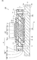
- the semiconductor device 102 as the second example of the semiconductor device 100 of the present embodiment basically has the same configuration as the semiconductor device 101 as the first example of FIG. Therefore, in FIG. 3, the same components as those in FIG. 2 are denoted by the same reference numerals, and the description thereof will not be repeated as long as the aspect is the same.
- the semiconductor device 102 in FIG. 3 differs from the semiconductor device 101 in FIG. 2 in the area of the first conductor layers 15A2 and 15A3 and the second conductor layers 15B2 and 15B3 in plan view.
- the first conductor layers 15A2 and 15A3 cover almost the entire region directly below the electronic component 12 in plan view, more specifically, for example, the entire region overlapping the electrode 22.
- the number of first through portions 16A is larger than that in FIG. 2 (seven in FIG. 3).
- the second conductor layers 15B2 and 15B3 are narrower than the semiconductor device 101.
- the first conductor layers 15A1 and 15A4 and the second conductor layers 15B1 and 15B4 are basically the same as those of the semiconductor device 101.
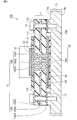
- a semiconductor device 103 as a third example of the semiconductor device 100 of the present embodiment basically has the same configuration as the semiconductor devices 101 and 102.
- the same components as those in FIGS. 2 and 3 are denoted by the same reference numerals, and the description thereof will not be repeated as long as the aspect is the same.
- the semiconductor device 103 in FIG. 4 is different from the semiconductor devices 101 and 102 in the area of the first conductor layers 15A2 and 15A3 and the second conductor layers 15B2 and 15B3 in plan view.
- the first conductor layers 15A2 and 15A3 extend from the region immediately below the electronic component 12 in a plan view to the region outside thereof, as shown in FIG. It is formed in a wider range than that. More specifically, the first conductor layers 15A2 and 15A3 in FIG. 4 are spread so as to overlap the entire region overlapping the first conductor layers 15A1 and 15A4, for example, and the number of the first through portions 16A is correspondingly increased. Are formed more than FIG. 3 (15 in FIG. 4). As a result, the second conductor layers 15B2 and 15B3 are narrower than the semiconductor devices 101 and 102.
- the first conductor layers 15A1 and 15A4 and the second conductor layers 15B1 and 15B4 are basically the same as those of the semiconductor device 101.
- the first conductor layer 15A and the second conductor layer 15B are viewed in plan view. Does not include opposing areas so as to overlap each other. However, also in the semiconductor device 103, at least the first conductor layer 15A and the second conductor layer 15B are disposed with an interval of, for example, 0.4 mm or more therebetween via the insulating layer 11C. For this reason, the one first member formed by connecting the first through portion 16A and the first conductor layer 15A to each other, and the second through portion 16B and the second conductor layer 15B are connected to each other. The one united second member is electrically insulated from each other.
- the semiconductor device 104 as the fourth example of the semiconductor device 100 of the present embodiment basically has the same configuration as the semiconductor device 101 as the first example of FIG. Therefore, in FIG. 5, the same components as those in FIG. 2 are denoted by the same reference numerals, and description thereof will not be repeated as long as the aspect is the same.
- the semiconductor device 104 in FIG. 5 is different from the semiconductor device 101 in FIG. 2 in the number of layers of the first conductor layer 15A and the second conductor layer 15B.
- the first conductor layer 15A is the first conductor layer 15A1, 15A2, 15A3, and the second conductor layer 15B is the second conductor layer 15B1. , 15B2 and 15B3.
- the first conductor layer 15A is a four-layered first conductor layer 15A1 to 15A4, and the second conductor layer 15B is a four-layered second conductor layer 15B1 to 15B4. It differs from the devices 101 to 103 in configuration.
- the first conductor layer 15A3 in FIG. 5 corresponds to the first conductor layer 15A4 in FIGS. 2 to 4
- the second conductor layer 15B3 in FIG. 5 corresponds to the second conductor layer 15B4 in FIGS. To do. Therefore, the first conductor layer 15A3 in FIG. 5 is formed on one main surface 11a similarly to the first conductor layer 15A4 in FIGS. 2 to 4, and the formed region and the area in plan view are the same.
- the second conductor layer 15B3 in FIG. 5 is formed on one main surface 11a similarly to the second conductor layer 15B4 in FIGS. 2 to 4, and the formed region and the area in plan view are the same.
- the first conductor layer 15A2 is disposed substantially at the center between the first conductor layer 15A1 and the first conductor layer 15A3 in the vertical direction of FIG. 5, and the second conductor layer 15B2 is the second conductor layer 15B2 in the vertical direction of FIG.
- the second conductor layer 15B1 and the second conductor layer 15B3 are disposed substantially at the center.
- the first conductor layer 15A and the second conductor layer 15B can have a configuration in which an arbitrary number of layers of three or more layers are stacked with a space therebetween. That is, the first conductor layer 15A and the second conductor layer 15B are not limited to three layers and four layers, and may be five layers or more. Also in the semiconductor device 104, the plane areas of the first conductor layer 15A2 and the second conductor layer 15B2 may be the same as those in FIGS.
- the semiconductor device 105 as the fifth example of the semiconductor device 100 of the present embodiment basically has the same configuration as the semiconductor device 101 as the first example of FIG. Therefore, in FIG. 6, the same components as those in FIG. 2 are denoted by the same reference numerals, and description thereof will not be repeated as long as the aspect is the same.
- the semiconductor device 105 in FIG. 6 includes the first heat transfer member 31 in at least one of the region between the printed circuit board 11 and the screw 14 and the region between the printed circuit board 11 and the heat radiating housing 13. Further, the semiconductor device 101 is different from the semiconductor device 101 of FIG.
- the region sandwiched between the second conductor layer 15B4 of the printed circuit board 11 and the head of the screw 14, and the second conductor layer 15B1 of the printed circuit board 11 The first heat transfer member 31 is disposed in both areas sandwiched between the heat dissipation casing 13 and the heat dissipation casing 13 directly below. However, the first heat transfer member 31 may be disposed only in one of these regions. As the first heat transfer member 31, insulating heat transfer grease or the like is preferably used.
- FIG. 6 shows an example in which the first heat transfer member 31 is applied to the semiconductor device 101 of FIG. 2, but the first heat transfer is applied to the semiconductor devices 102 to 104 of FIGS.
- the member 31 for application may be applied.
- FIG. 7 shows a heat transfer mode from the electronic component 12 in the region of the electronic device 12 and the printed board 11 of the semiconductor device 102 shown in FIG. 3, for example.
- a solid line arrow in the figure. Heat is transferred from the electronic component 12 to the heat dissipation housing 13 through the first heat dissipation path HA shown in FIG.
- heat generated in the electronic component 12 is transmitted through the electrode 22 and the joining member 23, and is transmitted from the electronic component 12 side to the heat radiating housing 13 side through the first through portion 16 ⁇ / b> A of the printed circuit board 11 therebelow. .
- the heat reaches the heat radiating housing 13 via the heat diffusion plate 25 and the insulating member 24, and is radiated from there to the outside of the semiconductor device.
- the first heat radiation path HA there is a path that travels in the horizontal direction along the first conductor layers 15A1, 15A2, 15A3, and 15A4 although solid arrows are not shown.
- a first heat dissipation path HA is formed by the first member.
- the electronic component 12 is mainly connected to the electronic component 12 as compared with the case where the electronic component 12 is not electrically connected and the heat dissipation path is provided only in a region away from the electronic component 12 in plan view.
- Heat can be radiated to the heat radiating housing 13 over a wide range by the first heat radiation path HA of the first member capable of conducting heat with high thermal conductivity. Therefore, the thermal resistance in the region between the electronic component 12 and the heat radiating housing 13 can be reduced, and the heat radiation efficiency from the electronic component 12 to the heat radiating housing 13 can be increased.
- the heat dissipation effect is higher in the semiconductor device 102 than in the semiconductor device 101 and in the semiconductor device 103 than in the semiconductor device 102.
- the plurality of first conductor layers 15A are connected to the plurality of second conductor layers 15B and the second conductor layers 15B that are spaced apart from each other, and the printed board 11 is moved in the vertical direction.
- a second heat dissipation path HB is formed by the second member with the second penetrating portion 16B extending in the direction.
- the second heat dissipation path HB is indicated by a dotted arrow in FIG. 7, and is mainly composed of a path that travels in the horizontal direction along the second conductor layers 15B2 and 15B3 and the second through portion 16B.
- the thermal resistance in the outer area in plan view of the first heat dissipation path HA is reduced, and the heat dissipation efficiency of this area is reduced. Can be increased. Therefore, the heat dissipation efficiency toward the heat dissipation housing 13 can be further increased.
- the heat radiation path is provided in both the region directly below the electronic component 12 and the outer region in plan view. For this reason, since heat can be radiated from the electronic component 12 to the heat radiating housing 13 in a wider range in plan view, the semiconductor device 100 can be miniaturized.
- the first heat dissipation path HA is not formed entirely in the plan view of the printed circuit board 11, and the second heat dissipation path HB is electrically connected from the first heat dissipation path HA so as not to be electrically connected to the first heat dissipation path HA.
- the reason for the electrical insulation is to prevent the electronic component 12 and the heat radiating housing 13 from being electrically short-circuited with each other via the screw 14 and the second through portion 16B.
- the semiconductor device 100 is required to be electrically insulated from the electronic component 12 and the heat dissipation housing 13 for safety. For this reason, the insulating member 24 is disposed between the other main surface 11b of the printed circuit board 11 and the heat radiating housing 13, and electrical insulation between the two is ensured.
- the first heat radiation path HA and the second heat radiation path HB are directly electrically connected without sandwiching the insulating layer 11C.
- the heat dissipation to the second heat dissipation path HB is slightly inferior.
- the first The thermal resistance of the portion of the insulating layer 11C extending from the heat dissipation path HA to the second heat dissipation path HB can be reduced, and transmission in the region of the insulating layer 11C from the first heat dissipation path HA to the second heat dissipation path HB is possible. A decrease in thermal efficiency can be suppressed.
- the first conductor layer 15A and the second conductor layer 15B as indicated by the left and right arrows in the figure are used as heat dissipation paths, and the first member such as the first conductor layer 15A and the second conductor layer 15B and the like Heat transfer efficiency between the two members can be increased.
- the insulating layer 11C in all regions is made thin, the standard printed circuit board 11 material cannot be used, which may increase manufacturing costs. Moreover, if the thickness of the entire printed circuit board 11 is reduced, there is a concern that the strength is weakened. Therefore, as a countermeasure, it is preferable that the region indicated by the thickness H2 is thicker than the thicknesses H1 and H3 (0.7 mm or more and 1.3 mm or less), because it is not necessary to conduct heat conduction so much and there is no problem even if the thermal resistance increases. . If it does in this way, the fall of the whole intensity
- first member constituting the first heat radiation path HA and the second member constituting the second heat radiation path HB are thin films of copper or a copper-based alloy as a main component, which is a substance having a low thermal resistance, The heat dissipation efficiency in the heat dissipation path can be further increased.
- first conductor layer 15A and the second conductor layer 15B are stacked with three or more layers spaced apart from each other, heat can be radiated in both directions by both the through portion 16 and the conductor layer 15, The heat dissipation efficiency can be further increased.
- the contact thermal resistance between the second conductor layer 15B and the second through portion 16B and the heat radiating housing 13 is reduced. can do.
- FIG. 7 shows the heat transfer mechanism of the semiconductor device 102 as an example. However, since the heat transfer is basically performed in the other semiconductor devices 101, 103, 104, and 105 in the same manner as in FIG. Is omitted.
- a semiconductor device 106 as a modified example (sixth example) of the present embodiment basically has the same configuration as semiconductor device 101 as the first example of FIG. Therefore, in FIG. 3, the same components as those in FIG. 2 are denoted by the same reference numerals, and the description thereof will not be repeated as long as the aspect is the same.
- a plurality (two in FIG. 8) of electronic components 12 are bonded on one main surface 11a of the printed circuit board 11, and those electronic components 12 are formed on the other main surface 11b.
- a common heat dissipating housing 13 is fixed.
- a single semiconductor device 101 is formed for each region where the electronic component 12 is disposed, and a plurality of semiconductor devices 101 are arranged to constitute a semiconductor device 106.
- a through hole 17 is formed in each region between a pair of adjacent semiconductor devices 101, and a screw 14 is provided in the through hole 17.
- the semiconductor device 106 can be further miniaturized. Moreover, if it does in this way, since it becomes the structure by which the thermal radiation path
- FIG. 8 shows an example in which two semiconductor devices 101 are combined as an example.
- the present invention is not limited to this.
- a semiconductor device 106 in which two or more semiconductor devices 102 to 105 are combined may be used, or a semiconductor device 106 having a configuration in which the semiconductor devices 101 to 105 are appropriately combined is formed. May be.
- Embodiment 2 FIG.
- an example of a specific structure of the semiconductor device 100 of the present embodiment will be described in detail with reference to FIGS.
- a semiconductor device 201 as a first example of the semiconductor device 100 of the present embodiment basically has the same configuration as the semiconductor device 101 of FIG. Therefore, in FIG. 9, the same components as those in FIG. 2 are denoted by the same reference numerals, and the description thereof will not be repeated as long as the aspect is the same.
- the semiconductor device 201 in FIG. 9 is fixed to the electronic component 12 and the second conductor layer 15B4 arranged on the most main surface 11a side of the printed board 11 among the plurality of second conductor layers 15B.
- the semiconductor device 101 is different from the semiconductor device 101 of FIG. 2 in that a heat radiating metal plate 26 as a first heat radiating metal plate is further provided.
- the heat radiating sheet metal 26 is a flat plate member made of a metal material having high thermal conductivity such as copper.
- the heat dissipating metal plate 26 is attached to both the uppermost surface of the package constituting the electronic component 12 whose positions in the vertical direction are greatly different from each other and the uppermost surface of the second conductor layer 15 ⁇ / b> B 4. It is bent at the end of the second conductor layer 15B4 and the region directly above the electronic component 12, and has a hat-like cross-sectional shape. The bending angle of the heat dissipating metal plate 26 shown in FIG.
- the heat generated by the electronic component 12 is natural from the surface of the package of the electronic component 12 to the surrounding air, except for the heat transmitted to the printed circuit board 11 and the heat radiating housing 13 side. Air cooled.
- a heat radiating metal plate 26 that is in contact with the uppermost surface of the electronic component 12 and the uppermost surface of the second conductor layer 15B4 is additionally disposed. The heat radiating metal plate 26 is fixed to the printed circuit board 11 with screws 14 immediately above the second conductor layer 15B4.
- part of the heat generated by the electronic component 12 is thermally conducted to the second conductor layer 15B4 side through the heat radiating metal plate 26, and is radiated from the second conductor layer 15B4 by the second heat radiation path of the second member. Heat can be transferred to the housing 13.
- the heat dissipation path from the electronic component 12 to the second conductor layer 15B4 is formed by the heat dissipation metal plate 26, the heat dissipation efficiency can be further enhanced.
- a semiconductor device 202 as a second example of the semiconductor device 100 of the present embodiment basically has the same configuration as the semiconductor device 201 of FIG. Therefore, in FIG. 10, the same components as those in FIG. 9 are denoted by the same reference numerals, and the description thereof will not be repeated as long as the aspect is the same.
- the semiconductor device 202 of FIG. 10 is different from that of FIG. 9 in that at least one of the electronic component 12 and the second conductor layer 15B4 is fixed to the heat radiating metal plate 26 via the second heat transfer member 32. Different from the semiconductor device 201.
- the semiconductor device 202 of FIG. 10 includes the second region in the region between the heat radiating metal plate 26 and the uppermost surface of the electronic component 12 and the region between the heat radiating metal plate 26 and the second conductor layer 15B4 of the printed board 11.
- 9 is different from the semiconductor device 201 of FIG. 9 in that the heat transfer member 32 is disposed.
- the second heat transfer is applied both to the region between the heat dissipating metal plate 26 and the uppermost surface of the electronic component 12 and to the region between the heat dissipating metal plate 26 and the second conductor layer 15B4 of the printed board 11.
- a member 32 is disposed.
- the second heat transfer member 32 is fixed in close contact with both the heat radiating sheet metal 26 and the electronic component 12.
- the second heat transfer member 32 is fixed in close contact with both the heat radiating metal plate 26 and the second conductor layer 15B4. However, the second heat transfer member 32 may be disposed only in one of the region fixed to the electronic component 12 and the region fixed to the second conductor layer 15B4.
- the uppermost surface portion of the electronic component 12 is constituted by a resin package, and electrical insulation between the electronic component mounted on the electronic component 12 and the metal heat radiating sheet metal 26 is ensured.
- an electrode is disposed on the uppermost surface portion of the electronic component 12, from the viewpoint of ensuring electrical insulation between the electronic component 12 and the heat radiating sheet metal 26, as shown in FIG. 12 and / or a region between the heat dissipating sheet metal 26 and the second conductor layer 15B4 of the printed board 11 so that the second heat transfer member 32 is sandwiched therebetween.
- the second heat transfer member 32 it is preferable to use, for example, a sheet formed by applying a heat-dissipating silicone resin.
- a sheet formed by applying a heat-dissipating silicone resin thereby, both the electrical insulation of the area
- a member having a high thermal conductivity in the planar direction such as a graphite sheet, which is installed on the entire surface of the heat radiating sheet metal 26 on the side facing the electronic component 12 is used as the second heat transfer member 32.
- the heat generated by the electronic component 12 is transmitted to the heat radiating metal plate 26 through the graphite sheet, and the route is transmitted through the graphite sheet to the region between the heat radiating metal plate 26 and the second conductor layer 15B4 of the printed board 11.
- These two paths can be transmitted to the second conductor layer 15B4. For this reason, the thermal resistance of the area
- a semiconductor device 203 as a third example of the semiconductor device 100 of the present embodiment basically has the same configuration as the semiconductor device 201 of FIG. Therefore, in FIG. 11, the same components as those in FIG. 9 are denoted by the same reference numerals, and description thereof will not be repeated as long as the aspect is the same.
- the semiconductor device 203 of FIG. 11 is different from the electronic component 12 in that a heat dissipation fin 27 is provided on the surface of the heat radiating sheet metal 26 directly above the electronic component 12 (on the upper side in the drawing). 9 different from the semiconductor device 201 of FIG.
- a semiconductor device 204 as a fourth example of the semiconductor device 100 of the present embodiment basically has the same configuration as the semiconductor device 106 of FIG. Therefore, in FIG. 11, the same components as those in FIG. 9 are denoted by the same reference numerals, and description thereof will not be repeated as long as the aspect is the same.
- the semiconductor device 204 in FIG. 12 is in contact with the respective electronic components 12 of the semiconductor device 101 arranged in a plurality (three in FIG. 12) as well as the semiconductor device 106 and the screw 14 disposed between the semiconductor devices 101.
- the semiconductor device 106 is different from the semiconductor device 106 in that a single large heat radiating metal plate 26 is disposed so as to straddle each of the second conductor layers 15B4. As in FIGS.
- the heat radiating metal plate 26 includes the electronic component 12 and the second conductor layer disposed closest to one main surface 11a of the printed circuit board 11 among the plurality of second conductor layers 15B. It is fixed to 15B4. However, instead of using a single large heat radiating metal plate 26 as shown in FIG. 12, a separate heat radiating metal plate 26 may be provided for each of the plurality of semiconductor devices 101.
- the adjacent semiconductor devices 101 share the same heat dissipation path, so that the semiconductor device 204 can be further downsized.
- the thermal resistance of the heat radiating metal plate 26 can be further reduced by making the heat radiating metal plate 26 thicker than the configuration of FIG. 12 or by increasing the area where the heat radiating metal plate 26 and the second conductor layer 15B4 are fixed. it can.
- the second heat transfer member 32 of FIG. 10 and / or the fins 27 of FIG. 11 may be added to the semiconductor device 204 of FIG. Also in this embodiment, the configuration of the conductor layer 15 as shown in FIGS. 3 to 5 may be employed.
- a path that transmits the heat radiating metal plate 26 is used. Can be added. For this reason, the presence of a heat dissipation path from the electronic component 12 to the second conductor layer 15B4 can reduce the thermal resistance between the electronic component 12 and the heat dissipation housing 13 and improve the heat dissipation performance of the semiconductor device. .
- Embodiment 3 FIG.
- an example of a specific structure of the semiconductor device 100 of the present embodiment will be described in detail with reference to FIGS.
- a semiconductor device 301 as a first example of the semiconductor device 100 of the present embodiment basically has the same configuration as the semiconductor device 201 of FIG. For this reason, in FIG. 9, the same components as those in FIG.
- the semiconductor device 301 of FIG. 13 includes a heat dissipating metal plate 28 as a flat plate-like second heat dissipating metal plate fixed to the electronic component 12 and one main surface of the printed circuit board 11 among a plurality of second conductor layers 15B.
- the semiconductor device 201 is different from the semiconductor device 201 of FIG. 9 in that the second conductor layer 15B4 disposed on the 11a side and the spacer 29 disposed between the heat radiating metal plates 28 are further provided.
- the heat radiating sheet metal 28 is flat.
- the heat radiating sheet metal 28 according to the present embodiment is similar to the heat radiating sheet metal 26 shown in FIG. 13 between the top surface of the electronic component 12 and the top surface of the second conductor layer 15B4. This means that the surface is not bent in consideration of the step in the vertical direction, and the surface is almost flat as a whole.
- the heat radiating sheet metal 28 extends flatly from the uppermost surface of the electronic component 12 to the uppermost surface of the second conductor layer 15B4 on the left and right sides of FIG.
- a gap is formed between the heat radiating metal plate 28 and the second conductor layer 15B4 directly above the second conductor layer 15B4. Arise. A member that fills this gap is a spacer 29. By disposing the spacer 29, the heat radiating metal plate 28 is placed on the uppermost surfaces of the spacer 29 and the electronic component 12 so as to bridge them.
- the spacer 29 is a cylindrical or rectangular parallelepiped member, for example, and is preferably made of a metal material having high thermal conductivity.
- the spacer 29 may be fixed to the region between the second conductor layer 15B4 and the heat radiating metal plate 28 by the screw 14. In this case, since the screw 14 penetrates the spacer 29, a through hole is formed in the central portion of the spacer 29 in plan view.
- a semiconductor device 302 as a second example of the semiconductor device 100 of the present embodiment basically has the same configuration as the semiconductor device 301 of FIG. For this reason, in FIG. 14, the same reference numerals are given to the same components as those in FIG.
- the semiconductor device 302 of FIG. 14 is different from the semiconductor device 301 of FIG. 13 in that a plate spring 33 is fixed to the heat radiating metal plate 28 by, for example, screws 14. The leaf spring 33 presses the electronic component 12 downward from the upper side of the heat radiating metal plate 28.
- FIGS. 13 and 14 show only the regions of the single semiconductor devices 301 and 302, the first embodiment (FIG. 8) and the second embodiment (FIG. 12) also in this embodiment.
- a configuration in which a plurality of electronic components 12 are included and the second heat dissipation path is shared among them may be employed.
- the configuration of the conductor layer 15 as shown in FIGS. 3 to 5, the fins 27 and the second heat transfer member 32 as shown in FIGS. 10 to 11 may be employed.
- the present embodiment provides the following operational effects in addition to the operational effects of the first embodiment.
- the heat radiating sheet metal 28 is flat, it is not necessary to perform bending to bend it like the heat radiating sheet metal 26 of the second embodiment, thereby reducing the processing cost. Can do. Since a distance is generated between the flat heat dissipating metal plate 28 and the second conductor layer 15B4 immediately below the flat heat dissipating metal plate 28, the thermal resistance between the heat dissipating metal plate 28 and the second conductor layer 15B4 is larger than that of the second embodiment. There are concerns. However, by increasing the cross-sectional area of the spacer 29 sandwiched between the heat radiating metal plate 28 and the second conductor layer 15B4 in plan view from above in FIG. The resistance can be set to be equal to or lower than the thermal resistance of the heat radiating sheet metal 26 of the second embodiment.
- the printed circuit board 11 is not only fixed to the heat radiating housing 13 by the screws 14 but also directed downward from the upper side of FIG. By being pressed, it is fixed to the heat radiating housing 13. For this reason, when attaching the printed circuit board 11 to the heat radiating housing 13, the thickness of the insulating member 24 suppresses the deformation that causes the printed circuit board 11 to warp upward in the drawing and the damage caused by the deformation. Can do. Further, when the heat radiating metal plate 28 presses the electronic component 12 downward, the insulating member 24 disposed between the printed board 11 and the heat radiating housing 13 can be crushed so as to be thinner. Thereby, the thermal resistance via the insulating member 24 between the printed circuit board 11 and the heat dissipation housing 13 can be reduced.
- the leaf spring 33 installed as shown in FIG. 14 presses the electronic component 12 downward from the upper side of the heat radiating sheet metal 28, thereby pressing downward on the printed circuit board 11 just below the electronic component 12.
- the pressure becomes larger. For this reason, deformation and breakage of the printed circuit board 11 can be more reliably suppressed, and thermal resistance via the insulating member 24 between the printed circuit board 11 and the heat radiating housing 13 can be further reduced. it can.
- the force for pressing the electronic component 12 downward increases as the vertical dimension of the spacer 29 in FIG. 13 is reduced (that is, as the height is lowered), and the vertical dimension of the spacer 29 in FIG. (That is, if the height is increased), it becomes smaller.
- the magnitude of the pressing force applied to the electronic component 12 by the heat radiating sheet metal 28 can be adjusted.
- Embodiment 4 FIG.
- an example of a specific structure of the semiconductor device 100 of the present embodiment will be described in detail with reference to FIGS.
- FIG. 15 shows a heat transfer mode from the electronic component 12 in the semiconductor device 401 as an example of the semiconductor device 100 according to the present embodiment by cutting out a part of the electronic component 12 and the printed board 11. .
- the semiconductor device 401 of the present embodiment has basically the same configuration as the semiconductor device 101 of FIG. Therefore, in FIG. 15, the same components as those in FIG. The semiconductor device 401 in FIG. 15 is different from the semiconductor device 101 in FIG. 2 in the number of first conductor layers 15A and the heat transfer mechanism from the first conductor layer 15A to the second conductor layer 15B.
- the first conductor layer 15A similar to the other examples is added to the first conductor layers 15A1, 15A2, 15A3, and 15A4, as well as the first conductor layers 15A5 and 15A5.
- the second conductor layer 15B has four layers of second conductor layers 15B1, 15B2, 15B3, and 15B4 as in the other examples.
- the printed circuit board includes five or more first conductor layers 15A.
- the semiconductor device 401 is different from the semiconductor device 101 in which the first conductor layer 15A and the second conductor layer 15B are both four layers.
- the first conductor layers 15A1, 15A2, 15A3, and 15A4 are laminated in this order from the lower layer to the upper layer in the same manner as in the above examples.
- the first conductor layer 15A5 and the first conductor layer 15A6 are sandwiched between the first conductor layer 15A2 and the first conductor layer 15A3, and the first conductor layer 15A5 is the first conductor layer 15A5. Is laminated below the conductor layer 15A6.
- the present invention is not limited thereto, and the first conductor layers 15A5 and 15A6 may be disposed, for example, between the first conductor layer 15A3 and the first conductor layer 15A4. These six first conductor layers 15A1 to 15A6 are laminated with a space therebetween.
- the first conductor layer 15A has a first surface on one or the other main surface 11a, 11b based on the distance between the first conductor layers 15A2, 15A3 in the first conductor layer 15A.
- the conductor layers 15A1 and 15A4 and the first conductor layers 15A2 and 15A3 adjacent to the conductor layers 15A1 and 15A4 are arranged such that the distance therebetween becomes smaller.
- the first conductor layer 15A5 and the first conductor layer 15A6 are sandwiched between the first conductor layer 15A2 and the first conductor layer 15A3.
- the first conductor layer on one or the other main surfaces 11a, 11b is determined based on the distance between a pair of adjacent first conductor layers 15A5 and the first conductor layer 15A6 inside the printed circuit board 11, for example.
- the distance between 15A1 and 15A4 and the first conductor layers 15A2 and 15A3 adjacent thereto is larger.
- the present invention is not limited to such a mode, and in the present embodiment, the distance between the first conductor layer 15A1 and the first conductor layer 15A2 is larger than the distance between the first conductor layer 15A5 and the first conductor layer 15A6. May be smaller.
- each of the first conductor layers 15A1, 15A2, 15A3, and 15A4 is formed as the same layer as each of the second conductor layers 15B1, 15B2, 15B3, and 15B4.
- the first conductor layers 15A1, 15A5, 15A6, and 15A4 are formed so as to extend over a wide range of one main surface 11a and the other main surface 11b from a region overlapping the electronic component 12 in a plan view to a region outside thereof. ing. For this reason, the first conductor layers 15A1 and 15A4 and the second conductor layers 15B1 and 15B4 that are spaced apart from each other are spread only in the outermost edge of the printed circuit board 11 and a relatively narrow area adjacent thereto. Is formed.
- the first conductor layers 15A2 and 15A3 are formed so as to extend only in a part of the region immediately below the electronic component 12, that is, in a relatively central portion of the electronic component 12 in plan view, at least in FIG. Yes.
- the second conductor layers 15B2 and 15B3 in FIG. 2 are arranged so as to extend to the inner region in plan view as compared with the second conductor layers 15B1 and 15B4. It is arranged to overlap.
- the first conductor layers 15A1, 15A5, 15A6, and 15A4 and the second conductor layers 15B2 and 15B3 partially overlap each other and are insulated between them.
- the layer 11C is interposed.
- the first heat transfer via 15AA is connected to the first conductor layer 15A other than the first conductor layer 15A. That is, as shown in FIG. 15, among the six first conductor layers 15A, the right end portion of the first conductor layer 15A6 inside the printed circuit board 11 (not exposed on the surface) and the other first conductors other than the first conductor layer 15A.
- the first heat transfer via 15AA extending in the vertical direction in the drawing in the region outside the electronic component 12 in plan view, with the right end of the uppermost first conductor layer 15A4 being one of the layers 15A Connected by. Further, as shown in FIG. 15, among the six first conductor layers 15A, the right end portion of the first conductor layer 15A5 inside the printed circuit board 11 (not exposed to the surface) and the other first conductors other than the first conductor layer 15A.
- the first heat transfer via 15AA extending in the vertical direction in the drawing in the region outside the electronic component 12 in plan view, with the right end of the lowermost first conductor layer 15A1 being one of the layers 15A Connected by.
- the first heat transfer via 15AA is not limited thereto, and may be a mode in which two first conductor layers 15A arranged at intervals in the printed circuit board 11 are connected to each other.
- the second heat transfer via 15BB is connected to the second conductor layer 15B other than the second conductor layer 15B (not exposed). That is, as shown in FIG. 15, among the four second conductor layers 15B, the left end portion of the second conductor layer 15B2 inside the printed circuit board 11 (not exposed to the surface) and the other second conductors other than that.
- the second heat transfer via 15BB is not limited thereto, and for example, the second conductor layer 15B formed on one or the other main surface of the printed circuit board 11 and the second conductor disposed inside the printed circuit board 11. It may be an aspect in which the layer 15B is connected.
- the first heat transfer via 15AA and the second heat transfer via 15BB are connected to each other by a conductor, like the first through portion 16A and the second through portion 16B. However, the first heat transfer via 15AA and the second heat transfer via 15BB do not penetrate through the entire printed circuit board 11 and have the first or second conductor layer inside the printed circuit board 11 as one end. , Different from the first through portion 16A and the second through portion 16B.
- the first heat transfer via 15AA and the second heat transfer via 15BB may be configured so that the entire interior is filled with a conductor, and only the outer wall surface extending in the vertical direction in the figure is covered with the conductor.
- the inside may be filled with an insulating material such as resin.
- FIG. 16 is a schematic perspective view of the portion where the first heat transfer via 15AA penetrates the second conductor layer 15B3 in FIG. 15 as seen from above.
- the second conductor layer 15B3 has an opening 15PH as a hole formed so as to penetrate the second conductor layer 15B3 in the vertical direction in the figure, and the second conductor layer 15B3 is formed so as to penetrate the opening 15PH.
- One heat transfer via 15AA extends in the vertical direction in the figure.
- the opening 15PH and the first heat transfer via 15PH are spaced from each other so as not to contact each other. This is because the first conductor layers 15A4 and 15A6 and the second conductor layer 15B3 need to be electrically insulated.
- the interval varies depending on the voltage handled by the semiconductor device 401, but is preferably 0.4 mm or more, for example.
- the first heat dissipation path HA indicated by a solid line in the drawing and the second heat dissipation path HB indicated by a dotted line in the figure are similar to those of the other embodiments.
- Heat is transferred from the upper layer to the lower layer.
- a temperature difference may occur between the right end portion of the first conductor layer 15A4 and the right end portion of the first conductor layer 15A6 due to a difference in thermal conductivity.
- the amount of heat conduction from the lower temperature layer of the two first conductor layers 15A to the second conductor layer 15B is reduced, and the efficiency of heat conduction is reduced.
- the first heat transfer via 15AA is provided between the right end of the first conductor layer 15A4 and the right end of the first conductor layer 15A6 as in the present embodiment.
- the first heat transfer via 15AA is used as the third heat dissipation path HD indicated by the chain line arrow in the figure, and heat is radiated between the first conductor layer 15A4 and the first conductor layer 15A6 in the vertical direction of the figure. Therefore, the temperature difference between the first conductor layer 15A4 and the first conductor layer 15A6 can be reduced, and the temperature distribution in the first conductor layer 15A can be made uniform.
- the heat conduction from there to the second conductor layer 15B3 is uniformly shown from the upper side and the lower side as shown in the fourth heat radiation path HE. To be made. Thereby, heat can be efficiently conducted from the first conductor layer 15A to the second conductor layer 15B as compared with the case where heat is unevenly distributed only on either the upper side or the lower side of the second conductor layer 15B3. it can.
- the heat is transferred through the third heat radiation path HD between the first conductor layer 15A4 and the first conductor layer 15A6, so that the first heat transfer is performed.
- the via 15AA generates heat.
- the generated heat is transmitted from the first heat transfer via 15AA to the second conductor layer 15B3 through the opening 15PH as shown in the fourth heat dissipation path HE.
- the efficiency of heat transfer between the first member and the second member can be increased.
- the first heat transfer via 15AA that connects the first conductor layer 15A4 and the first conductor layer 15A6, and the first conductor layer 15A1 and the first conductor layer 15A5 that are in contact with each other.
- These heat transfer vias 15AA are arranged separately. However, a structure in which these are connected without being divided may be used.
- the second heat transfer via 15BB basically has the same effects as described above.
- first conductor layers 15A may be seven or more.
- first heat transfer via 15AA and the second heat transfer via 15BB should not be arranged only on the right side of the electronic component 12 in FIG. 15 but may be arranged on the left side of the electronic component 12 as well.
- the electronic component 12 may be arranged around the left and right as well as the front and rear.
Abstract
This semiconductor device (101) is provided with: a printed board (11); an electronic component (12) which is arranged on top of the printed board (11); and a heat sink (13) which is arranged below the printed board (11). The printed board (11) comprises an insulating layer (11C) and conductor layers (15). Each one of a plurality of conductor layers (15) has a plurality of first conductor layers (15A) that are electrically connected to the electronic component (12) and a plurality of second conductor layers (15B) that are arranged at a distance from the plurality of first conductor layers (15A) so as to be electrically insulated therefrom. This semiconductor device (101) is also provided with: a first penetration part (16A) which is connected to the plurality of first conductor layers (15A) and extends from one main surface (11a) of the printed board (11) to the other main surface (11b); and a second penetration part (16B) which is connected to the plurality of second conductor layers (15B) and extends from the one main surface (11a) of the printed board (11) to the other main surface (11b). The first conductor layers (15A) and the second conductor layers (15B) at least partially overlap each other when viewed in plan, or alternatively, the first conductor layers (15A) and the second conductor layers (15B) are arranged at a distance from each other in a direction along the one main surface (11a).
Description
本発明は半導体装置に関し、特に、プリント基板上の電子部品から発生した熱をプリント基板を介して放熱させる半導体装置に関するものである。
The present invention relates to a semiconductor device, and more particularly to a semiconductor device that radiates heat generated from electronic components on a printed board through the printed board.
近年、車載機器などのパワーエレクトロニクス機器に用いられる半導体装置は、多機能化、高出力化、および小型化の傾向にある。これに伴い、半導体装置に実装される電子部品の単位体積あたりの発熱量は大きく上昇しており、高い放熱性能を有する半導体装置が望まれている。
In recent years, semiconductor devices used in power electronics equipment such as in-vehicle equipment tend to be multifunctional, high output, and downsized. Accordingly, the amount of heat generated per unit volume of electronic components mounted on the semiconductor device is greatly increased, and a semiconductor device having high heat dissipation performance is desired.
電子部品から発生する熱を放熱する半導体装置は、たとえば特開平6-77679号公報(特許文献1)および特開平11-345921号公報(特許文献2)に開示されている。これらの特許文献においては、プリント基板の上方に電子部品が接合されており、下方にヒートシンクが固定された構成となっている。プリント基板にはその一方の主表面から他方の主表面まで貫通するように形成された熱伝導経路が形成されている。この熱伝導経路により、電子部品から発生する熱が、熱伝導経路を経由してヒートシンクに伝わり、ヒートシンクから外部に放熱可能となっている。
Semiconductor devices that dissipate heat generated from electronic components are disclosed in, for example, Japanese Patent Application Laid-Open No. 6-77679 (Patent Document 1) and Japanese Patent Application Laid-Open No. 11-34592 (Patent Document 2). In these patent documents, an electronic component is joined above a printed circuit board, and a heat sink is fixed below. The printed circuit board has a heat conduction path formed so as to penetrate from one main surface to the other main surface. With this heat conduction path, heat generated from the electronic component is transmitted to the heat sink via the heat conduction path, and can be radiated from the heat sink to the outside.
特開平6-77679号公報の装置においてはプリント基板のうち電子部品の真下から離れたところのみに熱伝導経路が設けられており、特開平11-345921号公報においてはプリント基板のうち電子部品の真下のみに熱伝導経路が設けられている。このためいずれもプリント基板のうち伝熱可能な領域の面積が小さく、電子部品から伝導できる熱量が少ないため、電子部品からその下方のヒートシンクまでの領域の放熱性が十分でない。
In the apparatus disclosed in Japanese Patent Laid-Open No. 6-77679, a heat conduction path is provided only in the printed board away from directly below the electronic component. In Japanese Patent Laid-Open No. 11-34592, the electronic component of the printed board is provided. A heat conduction path is provided only underneath. For this reason, since the area of the heat transferable region of the printed circuit board is small and the amount of heat that can be conducted from the electronic component is small, the heat dissipation of the region from the electronic component to the heat sink below it is not sufficient.
本発明は、上記の課題に鑑みてなされたものであり、その目的は、電子部品を中心とした広範囲において、電子部品から放熱器への熱伝導が可能であり、電子部品の発熱に対する放熱性を向上させることが可能な半導体装置を提供することである。
The present invention has been made in view of the above problems, and its purpose is to enable heat conduction from an electronic component to a radiator over a wide range centering on the electronic component, and to dissipate heat generated by the electronic component. It is an object to provide a semiconductor device capable of improving the above.
本発明の半導体装置は、プリント基板と、その上の電子部品と、その下の放熱器とを備える。プリント基板は絶縁層と導体層とを含む。複数の導体層のそれぞれは、電子部品と電気的に接続された複数の第1の導体層と、複数の第1の導体層と互いに間隔をあけ、電気的に絶縁されて配置される複数の第2の導体層とを有する。複数の第1の導体層のそれぞれと接続され、プリント基板の一方の主表面から他方の主表面まで延びる第1の貫通部と、複数の第2の導体層のそれぞれと接続され、プリント基板の一方の主表面から他方の主表面まで延びる第2の貫通部とをさらに備える。第1の導体層と第2の導体層とは少なくとも一部において平面的に重なっているか、または一方の主表面に沿う方向に関して互いに間隔をあけて配置されている。
The semiconductor device of the present invention includes a printed circuit board, an electronic component thereon, and a radiator below it. The printed circuit board includes an insulating layer and a conductor layer. Each of the plurality of conductor layers includes a plurality of first conductor layers electrically connected to the electronic component, and a plurality of first conductor layers spaced apart from each other and electrically insulated. A second conductor layer. A plurality of first conductor layers connected to each of the first through-holes extending from one main surface of the printed circuit board to the other main surface; and connected to each of the plurality of second conductive layers; A second penetrating portion extending from one main surface to the other main surface. The first conductor layer and the second conductor layer at least partially overlap each other in a planar manner, or are spaced apart from each other in the direction along one main surface.
本発明によれば、電子部品の下方だけでなく電子部品を中心としその外側の領域を含む広範囲に放熱する経路を有する。放熱経路の範囲が広くなるため、電子部品から放熱器までの領域の熱抵抗を低減することができ、電子部品から放熱器への高い放熱性能を有する半導体装置を提供できる。
According to the present invention, there is a path for radiating heat over a wide range including not only the lower part of the electronic part but also the area outside the electronic part. Since the range of the heat dissipation path is widened, the thermal resistance in the region from the electronic component to the radiator can be reduced, and a semiconductor device having high heat dissipation performance from the electronic component to the radiator can be provided.
以下、一実施の形態について図に基づいて説明する。
実施の形態1.
図1は本実施の形態の半導体装置全体または一部の外観態様を示している。すなわち図1が半導体装置の一部である場合には、図1は半導体装置全体の一部のみを切り取った態様を示している。図1を参照して、本実施の形態の半導体装置100は、たとえばパワーエレクトロニクス機器に搭載される電力変換装置に用いられる。半導体装置100は、プリント基板11と、電子部品12と、放熱用筐体13と、ネジ14とを主に有している。 Hereinafter, an embodiment will be described with reference to the drawings.
Embodiment 1 FIG.
FIG. 1 shows the appearance of the whole or a part of the semiconductor device of this embodiment. That is, when FIG. 1 is a part of a semiconductor device, FIG. 1 shows a mode in which only a part of the whole semiconductor device is cut out. Referring to FIG. 1,semiconductor device 100 of the present embodiment is used for a power conversion device mounted on, for example, power electronics equipment. The semiconductor device 100 mainly includes a printed circuit board 11, an electronic component 12, a heat radiating housing 13, and screws 14.
実施の形態1.
図1は本実施の形態の半導体装置全体または一部の外観態様を示している。すなわち図1が半導体装置の一部である場合には、図1は半導体装置全体の一部のみを切り取った態様を示している。図1を参照して、本実施の形態の半導体装置100は、たとえばパワーエレクトロニクス機器に搭載される電力変換装置に用いられる。半導体装置100は、プリント基板11と、電子部品12と、放熱用筐体13と、ネジ14とを主に有している。 Hereinafter, an embodiment will be described with reference to the drawings.
Embodiment 1 FIG.
FIG. 1 shows the appearance of the whole or a part of the semiconductor device of this embodiment. That is, when FIG. 1 is a part of a semiconductor device, FIG. 1 shows a mode in which only a part of the whole semiconductor device is cut out. Referring to FIG. 1,
プリント基板11は、半導体装置100全体の土台をなす、たとえば平面視において矩形状を有する平板状の部材である。プリント基板11には後述する複数の配線すなわち導体層が形成されており、この複数の導体層は、電子部品12と、図示されない他の周辺回路部品とを、電気的に接続している。
The printed circuit board 11 is a flat plate member having a rectangular shape in plan view, for example, which forms the foundation of the entire semiconductor device 100. A plurality of wirings, that is, conductor layers, which will be described later, are formed on the printed circuit board 11. The plurality of conductor layers electrically connect the electronic component 12 and other peripheral circuit components not shown.
電子部品12は、プリント基板11の一方の主表面側すなわち図1の上側に接合されている。電子部品12は、MOSFET(Metal Oxide Semiconductor Field Effect Transistor)、IGBT(Insulated Gate Bipolar Transistor)、またはダイオードなどを含む半導体チップが樹脂で封止されたパッケージである。この半導体チップは大電力を制御するため、半導体装置100の動作時における電子部品12の発熱量は数ワットから数十ワットと大きい。このため半導体装置100の動作時には、水冷または空冷などにより半導体装置100を放熱する構造が必要となる。
The electronic component 12 is bonded to one main surface side of the printed circuit board 11, that is, the upper side in FIG. The electronic component 12 is a package in which a semiconductor chip including a MOSFET (Metal Oxide Semiconductor Field Effect Transistor), an IGBT (Insulated Gate Bipolar Transistor), or a diode is sealed with a resin. Since this semiconductor chip controls high power, the amount of heat generated by the electronic component 12 during operation of the semiconductor device 100 is as large as several watts to several tens of watts. For this reason, when the semiconductor device 100 is operated, a structure for radiating heat from the semiconductor device 100 by water cooling or air cooling is required.
放熱用筐体13は、プリント基板11の一方の主表面と反対側の他方の主表面側すなわち図1の下側に固定された、放熱器としての部材である。放熱用筐体13は、半導体装置100に別途設置される図示されない空冷または水冷などの装置によって一定温度以下に冷却された状態が保たれる。放熱用筐体13は半導体装置100の構成によっては、筐体ではなく、ヒートシンクまたはヒートパイプなどの放熱用機器を使用することもできる。しかし以降においては放熱器は放熱用筐体13であるものとして説明がなされる。
The heat radiating housing 13 is a member as a heat radiator fixed to the other main surface side opposite to one main surface of the printed circuit board 11, that is, the lower side in FIG. The heat dissipating housing 13 is kept cooled to a certain temperature or lower by a device such as air cooling or water cooling (not shown) separately installed in the semiconductor device 100. Depending on the configuration of the semiconductor device 100, the heat radiating housing 13 may be a heat radiating device such as a heat sink or a heat pipe instead of the housing. However, in the following description, the radiator is assumed to be the heat radiating housing 13.
ネジ14は、プリント基板11を放熱用筐体13に接触するように固定する固定部材として用いられる。固定部材はプリント基板11と放熱用筐体13とを固定できればよいため、ネジ14に限らず、たとえばリベットなどの他の接続部材が代用されてもよい。また図1においてネジ14は、平面視において概ねプリント基板11の4つの角部に隣接する領域に配置されている。しかしネジ14の設置本数は4本に限らず、プリント基板11に放熱用筐体13を締結により固定することが可能である限り任意の本数とすることができる。ネジ14などの固定部材によりプリント基板11と放熱用筐体13とが固定されることにより、電子部品12で発生した熱をプリント基板11を介して放熱用筐体13まで伝導させ放熱用筐体13から半導体装置100の外部へ放熱させることができる。
The screw 14 is used as a fixing member that fixes the printed circuit board 11 so as to contact the heat radiating housing 13. Since the fixing member only needs to fix the printed circuit board 11 and the heat radiating housing 13, the connecting member is not limited to the screw 14, and other connecting members such as rivets may be used instead. Further, in FIG. 1, the screw 14 is disposed in a region that is generally adjacent to the four corners of the printed circuit board 11 in plan view. However, the number of screws 14 is not limited to four, and may be any number as long as the heat dissipating housing 13 can be fixed to the printed board 11 by fastening. By fixing the printed circuit board 11 and the heat radiating housing 13 by a fixing member such as a screw 14, heat generated in the electronic component 12 is conducted to the heat radiating housing 13 through the printed circuit board 11, and the heat radiating housing. The heat can be radiated from 13 to the outside of the semiconductor device 100.
図2~図6は、図1の2つのネジ14と、電子部品12とを通るように切断された断面の態様の例を示している。このことはこれ以降の各実施の形態(各例)において示される断面図においても同様である。次に、図2~図6を用いて、本実施の形態の半導体装置100の具体的な構造の例を詳細に説明する。
2 to 6 show examples of cross-sectional aspects cut so as to pass through the two screws 14 of FIG. 1 and the electronic component 12. The same applies to the sectional views shown in the following embodiments (each example). Next, an example of a specific structure of the semiconductor device 100 of the present embodiment will be described in detail with reference to FIGS.
図2を参照して、本実施の形態の半導体装置100の第1例としての半導体装置101においては、プリント基板11が、一方の主表面11aと、その反対側の他方の主表面11bとを有している。そしてプリント基板11は、絶縁層11Cと、複数の導体層15とを含む構成を有している。
Referring to FIG. 2, in semiconductor device 101 as a first example of semiconductor device 100 of the present embodiment, printed circuit board 11 includes one main surface 11a and the other main surface 11b on the opposite side. Have. The printed board 11 has a configuration including an insulating layer 11 </ b> C and a plurality of conductor layers 15.
絶縁層11Cは、プリント基板11の本体をなす部材である。絶縁層11Cはたとえばガラス繊維とエポキシ樹脂とにより構成されているが、これに限定することなく、たとえばアラミド樹脂とエポキシ樹脂とにより構成されていてもよい。あるいは絶縁層11Cはセラミックス材料により形成されてもよい。
The insulating layer 11 </ b> C is a member that forms the main body of the printed circuit board 11. The insulating layer 11C is made of, for example, glass fiber and an epoxy resin, but is not limited thereto, and may be made of, for example, an aramid resin and an epoxy resin. Alternatively, the insulating layer 11C may be formed of a ceramic material.
導体層15は、絶縁層11Cの主表面、すなわちプリント基板11の一方の主表面11aおよび他方の主表面11bに沿うように拡がっている。導体層15は、電子部品12側すなわちプリント基板11の上側から、放熱用筐体13側すなわちプリント基板11の下側まで、絶縁層11Cの一部を介して複数積層されている。すなわち複数積層される導体層15のうち一の導体層15とこれに隣接する他の導体層15との間には、絶縁層11Cの一部が挟まれている。半導体装置101においては導体層15は、図の上下方向に関して互いに間隔をあけて4層、積層されている。
The conductor layer 15 extends along the main surface of the insulating layer 11C, that is, along one main surface 11a and the other main surface 11b of the printed board 11. A plurality of conductor layers 15 are laminated through a part of the insulating layer 11C from the electronic component 12 side, that is, the upper side of the printed board 11 to the heat radiating housing 13 side, that is, the lower side of the printed board 11. That is, a part of the insulating layer 11 </ b> C is sandwiched between one conductor layer 15 among the plurality of conductor layers 15 stacked and another conductor layer 15 adjacent thereto. In the semiconductor device 101, the conductor layer 15 is laminated in four layers at intervals in the vertical direction of the figure.
またこの4層積層される導体層15は、図の左右方向に関して、電子部品12と電気的に接続された複数すなわち4層の第1の導体層15Aと、第1の導体層15Aとの間に互いに間隔をあけ、電気的に絶縁されて(たとえば絶縁層11Cを介して)配置されている複数すなわち4層の第2の導体層15Bとを有している。第1の導体層15Aおよび第2の導体層15Bは、いずれもプリント基板11の一方の主表面11aおよび他方の主表面11bに沿うように拡がっている。電子部品12はプリント基板11の平面視における比較的中央の部分に接合されるため、電子部品12と電気的に接続される第1の導体層15Aは、プリント基板11の比較的中央の部分に配置されている。これに対して、第1の導体層15Aとの間に絶縁層11Cを介して配置されている第2の導体層15Bは、第1の導体層15Aとは電気的に接続されておらず電気的に分離された態様であり、プリント基板11の比較的外側の部分に配置されている。
The four conductor layers 15 are laminated between the first conductor layer 15A and a plurality of first conductor layers 15A electrically connected to the electronic component 12 and the first conductor layer 15A in the left-right direction in the figure. And a plurality of, that is, four second conductor layers 15B, which are electrically insulated (for example, via the insulating layer 11C) and spaced apart from each other. The first conductor layer 15A and the second conductor layer 15B both extend along one main surface 11a and the other main surface 11b of the printed circuit board 11. Since the electronic component 12 is bonded to a relatively central portion of the printed circuit board 11 in a plan view, the first conductor layer 15A electrically connected to the electronic component 12 is formed on the relatively central portion of the printed circuit board 11. Is arranged. On the other hand, the second conductor layer 15B disposed between the first conductor layer 15A and the first conductor layer 15A via the insulating layer 11C is not electrically connected to the first conductor layer 15A. And is arranged in a relatively outer portion of the printed circuit board 11.
第1の導体層15Aは、図の下層(放熱用筐体13側)から上層(電子部品12側)へ向けて、第1の導体層15A1、第1の導体層15A2、第1の導体層15A3、第1の導体層15A4の順に積層されている。また第2の導体層15Bは、図の下層(放熱用筐体13側)から上層(電子部品12側)へ向けて、第2の導体層15B1、第2の導体層15B2、第2の導体層15B3、第2の導体層15B4の順に積層されている。第1の導体層15A1と第2の導体層15B1とは同一の層として形成されている。同様に、第1の導体層15A2および第2の導体層15B2、第1の導体層15A3および第2の導体層15B3、ならびに第1の導体層15A4および第2の導体層15B4のそれぞれは、いずれも同一の層として形成されている。このように同一の層として並ぶ第1の導体層15Aと第2の導体層15Bとは、一方の主表面11aに沿う図の左右方向に関して互いに間隔をあけて配置されている。同一の層であるたとえば第1の導体層15A2(15A3)と第2の導体層15B2(15B3)との間隔は、半導体装置101の扱う電圧によって変化するが、たとえば0.4mm以上である。
The first conductor layer 15A has a first conductor layer 15A1, a first conductor layer 15A2, and a first conductor layer from the lower layer (radiation housing 13 side) to the upper layer (electronic component 12 side) in the figure. 15A3 and the first conductor layer 15A4 are stacked in this order. In addition, the second conductor layer 15B extends from the lower layer (heat dissipating housing 13 side) to the upper layer (electronic component 12 side) in the figure, the second conductor layer 15B1, the second conductor layer 15B2, and the second conductor. The layer 15B3 and the second conductor layer 15B4 are stacked in this order. The first conductor layer 15A1 and the second conductor layer 15B1 are formed as the same layer. Similarly, each of the first conductor layer 15A2 and the second conductor layer 15B2, the first conductor layer 15A3 and the second conductor layer 15B3, and the first conductor layer 15A4 and the second conductor layer 15B4 Are also formed as the same layer. As described above, the first conductor layer 15A and the second conductor layer 15B arranged as the same layer are arranged at a distance from each other in the horizontal direction of the drawing along the one main surface 11a. The distance between the first conductor layer 15A2 (15A3) and the second conductor layer 15B2 (15B3), which are the same layer, varies depending on the voltage handled by the semiconductor device 101, but is, for example, 0.4 mm or more.
図2においては、第1の導体層15A1および第2の導体層15B1は、プリント基板11の他方の主表面11b上に形成されている。第1の導体層15A2,15A3および第2の導体層15B2,15B3は、互いに他の導体層との間隔を保ちつつ、プリント基板11の内部に、絶縁層11Cに埋もれるように配置されている。第1の導体層15A4および第2の導体層15B4は、プリント基板11の一方の主表面11a上に形成されている。
In FIG. 2, the first conductor layer 15A1 and the second conductor layer 15B1 are formed on the other main surface 11b of the printed circuit board 11. The first conductor layers 15A2 and 15A3 and the second conductor layers 15B2 and 15B3 are disposed inside the printed board 11 so as to be buried in the insulating layer 11C while maintaining a distance from the other conductor layers. The first conductor layer 15A4 and the second conductor layer 15B4 are formed on one main surface 11a of the printed board 11.
図2に示すように、互いに積層された第1の導体層15Aは、プリント基板11内部の互いに隣接する1対の第1の導体層15A同士の距離より、一方または他方の主表面11a,11b上の第1の導体層15Aとそれに隣接する第1の導体層15Aとの距離の方が小さくなるように配置される。具体的には、第1の導体層15A1と第1の導体層15A2との図2の上下方向の距離、および第1の導体層15A3と第1の導体層15A4との図2の上下方向の距離は、第1の導体層15A2と第1の導体層15A3との図2の上下方向の距離よりも小さい。以上は第1の導体層15Aと同一の層として形成される第2の導体層15Bについても同様である。すなわち第2の導体層15B1と第2の導体層15B2との図2の上下方向の距離、および第2の導体層15B3と第2の導体層15B4との図2の上下方向の距離は、第2の導体層15B2と第2の導体層15B3との図2の上下方向の距離よりも小さい。
As shown in FIG. 2, the first conductor layers 15 </ b> A stacked on each other have one or the other main surfaces 11 a and 11 b based on the distance between the pair of first conductor layers 15 </ b> A adjacent to each other inside the printed circuit board 11. The first conductor layer 15A and the first conductor layer 15A adjacent to the first conductor layer 15A are arranged such that the distance between them is smaller. Specifically, the vertical distance in FIG. 2 between the first conductor layer 15A1 and the first conductor layer 15A2 and the vertical distance in FIG. 2 between the first conductor layer 15A3 and the first conductor layer 15A4. The distance is smaller than the vertical distance in FIG. 2 between the first conductor layer 15A2 and the first conductor layer 15A3. The same applies to the second conductor layer 15B formed as the same layer as the first conductor layer 15A. That is, the distance between the second conductor layer 15B1 and the second conductor layer 15B2 in the vertical direction in FIG. 2 and the distance between the second conductor layer 15B3 and the second conductor layer 15B4 in FIG. The distance between the second conductor layer 15B2 and the second conductor layer 15B3 in the vertical direction in FIG. 2 is smaller.
より具体的には、第1の導体層15A1と第1の導体層15A2との図2の上下方向の距離、および第1の導体層15A3と第1の導体層15A4との図2の上下方向の距離はたとえば0.2mm程度であり、概ね0.1mm以上0.3mm以下である。また第1の導体層15A2と第1の導体層15A3との図2の上下方向の距離はたとえば1.0mm程度であり、概ね0.7mm以上1.3mm以下である。上記距離については第2の導体層15Bについても第1の導体層15Aと同様のことがいえる。
More specifically, the vertical distance in FIG. 2 between the first conductor layer 15A1 and the first conductor layer 15A2 and the vertical direction in FIG. 2 between the first conductor layer 15A3 and the first conductor layer 15A4. The distance is, for example, about 0.2 mm, and is generally not less than 0.1 mm and not more than 0.3 mm. The distance in the vertical direction in FIG. 2 between the first conductor layer 15A2 and the first conductor layer 15A3 is, for example, about 1.0 mm, and is generally not less than 0.7 mm and not more than 1.3 mm. Regarding the distance, the same can be said for the second conductor layer 15B as for the first conductor layer 15A.
第1の導体層15A1,15A4は、平面視における電子部品12と重なる領域からその外側の領域まで、一方の主表面11aおよび他方の主表面11bの広い範囲に拡がるように形成されている。このため第1の導体層15A1,15A4と互いに間隔をあけて配置される第2の導体層15B1,15B4は、プリント基板11の平面視における最外縁およびそれに隣接する比較的狭い領域のみに拡がるように形成されている。これに対し、第1の導体層15A2,15A3は、少なくとも図2においては、電子部品12の真下の一部の領域すなわち平面視における電子部品12の比較的中央部のみに拡がるように形成されている。このため図2の第2の導体層15B2,15B3は、第2の導体層15B1,15B4に比べて平面視における内側の領域まで拡がるように配置されており、電子部品12の一部と平面的に重なるように配置されている。
The first conductor layers 15A1 and 15A4 are formed so as to extend over a wide range of one main surface 11a and the other main surface 11b from a region overlapping the electronic component 12 in a plan view to a region outside thereof. For this reason, the first conductor layers 15A1 and 15A4 and the second conductor layers 15B1 and 15B4 that are spaced apart from each other are spread only in the outermost edge of the printed circuit board 11 and a relatively narrow area adjacent thereto. Is formed. On the other hand, the first conductor layers 15A2 and 15A3 are formed so as to extend only in a part of the region immediately below the electronic component 12, that is, in a relatively central portion of the electronic component 12 in plan view, at least in FIG. Yes. For this reason, the second conductor layers 15B2 and 15B3 in FIG. 2 are arranged so as to extend to the inner region in plan view as compared with the second conductor layers 15B1 and 15B4. It is arranged to overlap.
その結果、第1の導体層15Aと第2の導体層15Bとは少なくとも一部において平面的に互いに重なっていてもよい。具体的には、図2においては、たとえば第1の導体層15A4と、その下側に隣接する第2の導体層15B3とは、部分的に互いに対向するように重なっており、両者の間に絶縁層11Cが介在している。すなわち第1の導体層15A4と第2の導体層15B3とは、図2の上下方向に関して互いに対向している。同様に、たとえば第1の導体層15A1と、その上側に隣接する第2の導体層15B2とは、図2の上下方向に関して部分的に互いに対向するように重なっており、両者の間に絶縁層11Cが介在している。図2に示すように、複数の第1の導体層15Aと複数の第2の導体層15Bとは、電子部品12の周囲すなわち電子部品12と図の左右方向に関して隣接する領域において、平面的に互いに重なる領域を備えることが好ましい。
As a result, the first conductor layer 15A and the second conductor layer 15B may overlap each other in a planar manner at least partially. Specifically, in FIG. 2, for example, the first conductor layer 15A4 and the second conductor layer 15B3 adjacent to the lower side of the first conductor layer 15A4 partially overlap each other, and between them, An insulating layer 11C is interposed. That is, the first conductor layer 15A4 and the second conductor layer 15B3 face each other in the vertical direction of FIG. Similarly, for example, the first conductor layer 15A1 and the second conductor layer 15B2 adjacent to the upper side of the first conductor layer 15A1 overlap each other partially in the vertical direction in FIG. 11C is interposed. As shown in FIG. 2, the plurality of first conductor layers 15 </ b> A and the plurality of second conductor layers 15 </ b> B are planarly arranged around the electronic component 12, that is, in a region adjacent to the electronic component 12 in the left-right direction in the drawing. It is preferable to provide areas that overlap each other.
複数の導体層15すなわち第1の導体層15Aおよび第2の導体層15Bは、特にたとえば絶縁層11Cが樹脂材料からなる場合には、たとえば銅の薄膜により形成されることが好ましい。銅の薄膜からなる導体層15は一般的に十数μm以上数百μm程度の厚みを有する。導体層15を厚くするほど、一方の主表面11aなどに沿う水平方向へ熱を広範囲に広げることが可能となり、半導体装置101としての放熱性能がより向上する。
The plurality of conductor layers 15, that is, the first conductor layer 15A and the second conductor layer 15B are preferably formed of, for example, a copper thin film, particularly when the insulating layer 11C is made of a resin material, for example. The conductor layer 15 made of a copper thin film generally has a thickness of about 10 to several hundred μm. As the conductor layer 15 becomes thicker, heat can be spread over a wide range in the horizontal direction along the one main surface 11a and the like, and the heat dissipation performance as the semiconductor device 101 is further improved.
但し当該導体層15は、特にたとえば絶縁層11Cがセラミックス材料からなる場合には、銅または銀を主成分とする合金の薄膜として形成されてもよい。ただし絶縁層11Cが樹脂材料からなる場合においても、導体層15が銅または銀を主成分とする合金の薄膜により形成されてもよい。すなわち導体層15(第1の導体層15Aおよび第2の導体層15B)は、銅の薄膜、銅を主成分とする合金の薄膜、銀を主成分とする合金の薄膜からなる群から選択されるいずれかである。
However, the conductor layer 15 may be formed as a thin film of an alloy mainly composed of copper or silver, particularly when the insulating layer 11C is made of a ceramic material, for example. However, even when the insulating layer 11C is made of a resin material, the conductor layer 15 may be formed of a thin film of an alloy mainly composed of copper or silver. That is, the conductor layer 15 (the first conductor layer 15A and the second conductor layer 15B) is selected from the group consisting of a copper thin film, a copper alloy thin film, and a silver alloy thin film. One of them.
プリント基板11には、複数の配線として、上記の導体層15のほか、貫通部16が形成されている。貫通部16は、プリント基板11の一方の主表面11aから他方の主表面11bに達するように、一方の主表面11aおよび他方の主表面11bに交差(たとえば直交)するように延びている。
The printed circuit board 11 is formed with a through portion 16 in addition to the conductor layer 15 as a plurality of wirings. The penetrating portion 16 extends so as to intersect (for example, orthogonally cross) the one main surface 11a and the other main surface 11b so as to reach the other main surface 11b from the one main surface 11a of the printed board 11.
貫通部16は、第1の貫通部16Aと、第2の貫通部16Bとを有している。第1の貫通部16Aは、第1の導体層15A1,15A2,15A3,15A4に交差するように、互いに間隔をあけて複数(図2においては5本)形成されている。第1の貫通部16Aは、第1の導体層15A1から第1の導体層15A4に達するようにプリント基板11に形成されたビアホールの内部を充填するように形成された導体部分であり、複数の第1の導体層15A1,15A2,15A3,15A4のそれぞれと互いに電気的に接続されている。基本的に第1の貫通部16Aは、銅または銅を主成分とする合金により形成されている。これにより、第1の貫通部16Aと、複数の第1の導体層15A1,15A2,15A3,15A4のそれぞれとは互いに電気的および機械的に接続されており、これらがあたかも1つのまとまった第1部材を構成するように配置されている。
The penetration part 16 has a first penetration part 16A and a second penetration part 16B. A plurality (five in FIG. 2) of first through portions 16A are formed at intervals so as to intersect the first conductor layers 15A1, 15A2, 15A3, and 15A4. The first through portion 16A is a conductor portion formed so as to fill the inside of the via hole formed in the printed circuit board 11 so as to reach the first conductor layer 15A4 from the first conductor layer 15A1. The first conductor layers 15A1, 15A2, 15A3, and 15A4 are electrically connected to each other. Basically, the first through portion 16A is made of copper or an alloy containing copper as a main component. As a result, the first through portion 16A and each of the plurality of first conductor layers 15A1, 15A2, 15A3, and 15A4 are electrically and mechanically connected to each other. It arrange | positions so that a member may be comprised.
互いに隣り合う第1の貫通部16A同士の間隔は、たとえば0.5mm以上1.0mm以下である。また第1の貫通部16Aは平面視においてたとえば円形であり、その円形の直径すなわち図2における第1の貫通部16Aの左右方向の幅はたとえば0.2mm以上0.3mm以下であることが好ましい。
The interval between the first through portions 16A adjacent to each other is, for example, not less than 0.5 mm and not more than 1.0 mm. The first through portion 16A is, for example, circular in plan view, and the diameter of the circle, that is, the width in the left-right direction of the first through portion 16A in FIG. 2 is preferably 0.2 mm or more and 0.3 mm or less, for example. .
また第2の貫通部16Bは、平面視における第1の貫通部16Aの外側に配置されている。具体的には、プリント基板11には、平面視における電子部品12よりも外側の領域において、一方の主表面11aから他方の主表面11bに達するスルーホール17が形成されている。このスルーホール17の内壁部に、筒状の導体膜としての第2の貫通部16Bが形成されている。スルーホール17は、第2の導体層15B1,15B2,15B3,15B4に交差するように接続されているため、スルーホール17内の第2の貫通部16Bは、第2の導体層15B1,15B2,15B3,15B4に交差するように接続されている。このため第2の貫通部16Bは、第2の導体層15B1,15B2,15B3,15B4と互いに電気的に接続されている。基本的に第2の貫通部16Bは、銅または銅を主成分とする合金により形成されている。これにより、第2の貫通部16Bと、複数の第2の導体層15B1,15B2,15B3,15B4のそれぞれとは互いに電気的および機械的に接続されており、これらがあたかも1つのまとまった第2部材を構成するように配置されている。
Further, the second penetrating portion 16B is disposed outside the first penetrating portion 16A in plan view. Specifically, a through hole 17 is formed in the printed board 11 so as to reach from the one main surface 11a to the other main surface 11b in a region outside the electronic component 12 in a plan view. A second through portion 16 </ b> B as a cylindrical conductor film is formed on the inner wall portion of the through hole 17. Since the through hole 17 is connected so as to intersect the second conductor layers 15B1, 15B2, 15B3, and 15B4, the second through portion 16B in the through hole 17 is connected to the second conductor layers 15B1, 15B2, and 15B2. It is connected so as to cross 15B3 and 15B4. Therefore, the second through portion 16B is electrically connected to the second conductor layers 15B1, 15B2, 15B3, and 15B4. Basically, the second through portion 16B is formed of copper or an alloy containing copper as a main component. As a result, the second through portion 16B and each of the plurality of second conductor layers 15B1, 15B2, 15B3, and 15B4 are electrically and mechanically connected to each other. It arrange | positions so that a member may be comprised.
スルーホール17の内部には、固定部材としてのネジ14が配置されている。ネジ14は一方の主表面11aから他方の主表面11bに達しプリント基板11を貫通し、さらにその下側の放熱用筐体13の内部まで達するように、図2の上下方向に延びている。したがってネジ14は第2の貫通部16Bの内部に設けられている。これによりネジ14は、プリント基板11を放熱用筐体13に固定している。ネジ14の頭の部分は第2の導体層15B4と接触するように配置されており、かつネジ14の延びる部分の表面は第2の貫通部16Bと接触するように配置されていてもよい。
A screw 14 as a fixing member is disposed inside the through hole 17. The screw 14 extends in the vertical direction in FIG. 2 so as to reach from the one main surface 11a to the other main surface 11b, penetrate the printed circuit board 11, and reach the inside of the heat dissipating housing 13 below. Therefore, the screw 14 is provided inside the second through portion 16B. Accordingly, the screw 14 fixes the printed circuit board 11 to the heat radiating housing 13. The head portion of the screw 14 may be disposed so as to be in contact with the second conductor layer 15B4, and the surface of the extending portion of the screw 14 may be disposed so as to be in contact with the second through portion 16B.
その他、半導体装置101には以下の各部材が配置されている。電子部品12には電極22が形成されている。電極22は、電子部品12の内部と外部との通電、および放熱を可能とすべく配置されている。電極22は電子部品12の下側の面の一部に埋もれるように配置されているが、このような態様に限られない。
In addition, the following members are arranged in the semiconductor device 101. An electrode 22 is formed on the electronic component 12. The electrode 22 is disposed so as to enable energization and heat dissipation between the inside and the outside of the electronic component 12. The electrode 22 is disposed so as to be buried in a part of the lower surface of the electronic component 12, but is not limited to such a mode.
電子部品12の電極22と、プリント基板11の第1の導体層15A4との間には接合部材23が配置されており、この接合部材23により、電極22と第1の導体層15A4とが互いに接合されている。接合部材23が電極22と第1の導体層15A4とを互いに接合することにより、電子部品12とプリント基板11とが互いに接合固定されている。
A bonding member 23 is disposed between the electrode 22 of the electronic component 12 and the first conductor layer 15A4 of the printed circuit board 11, and the electrode 22 and the first conductor layer 15A4 are mutually connected by the bonding member 23. It is joined. The joining member 23 joins the electrode 22 and the first conductor layer 15A4 to each other, whereby the electronic component 12 and the printed board 11 are joined and fixed to each other.
接合部材23は、はんだなどの、電気抵抗が小さくかつ熱伝導率が高い材料が用いられることが好ましい。このようにすれば接合部材23は、電子部品12の電極22とプリント基板11の第1の導体層15Aとを接合するように固定することで、電子部品12とプリント基板11とを接合固定することができる。
The joining member 23 is preferably made of a material having a low electrical resistance and a high thermal conductivity, such as solder. In this way, the bonding member 23 bonds and fixes the electronic component 12 and the printed board 11 by fixing the electrode 22 of the electronic component 12 and the first conductor layer 15A of the printed board 11 to be bonded. be able to.
プリント基板11の一方の主表面11aの一部および図2に示されないが他方の主表面11bの一部には、レジスト層21が配置されている。具体的には、たとえば電子部品12の最外縁の外側に隣接する領域からその内側に隣接する領域にかけて、レジスト層21が電子部品12とプリント基板11との間に挟まれるように配置されている。レジスト層21は、はんだなどの接合部材23の平面視における外側の領域に配置されている。レジスト層21ははんだなどの接合部材23の濡れ広がりを抑制しており、かつ電子部品12の外側の領域における電子部品12と第1の導体層15A4との電気的絶縁を簡易的に確保している。
A resist layer 21 is disposed on a part of one main surface 11a of the printed circuit board 11 and a part of the other main surface 11b (not shown in FIG. 2). Specifically, for example, the resist layer 21 is disposed so as to be sandwiched between the electronic component 12 and the printed circuit board 11 from a region adjacent to the outside of the outermost edge of the electronic component 12 to a region adjacent to the inside thereof. . The resist layer 21 is disposed in an outer region in a plan view of the joining member 23 such as solder. The resist layer 21 suppresses the wetting and spreading of the joining member 23 such as solder, and easily secures electrical insulation between the electronic component 12 and the first conductor layer 15A4 in the region outside the electronic component 12. Yes.
レジスト層21の素材は樹脂材料であるため、レジスト層21が電子部品12とプリント基板11との間の領域に挟まれれば、その部分において電子部品12からプリント基板11への熱伝導性が低下する。そのため、ネジ14と接触する領域およびそれに隣接する領域においては、一方の主表面11a上であってもレジスト層21は除去されていることが好ましい。
Since the material of the resist layer 21 is a resin material, if the resist layer 21 is sandwiched between regions of the electronic component 12 and the printed circuit board 11, the thermal conductivity from the electronic component 12 to the printed circuit board 11 decreases at that portion. To do. Therefore, the resist layer 21 is preferably removed even on the one main surface 11a in the region in contact with the screw 14 and the region adjacent thereto.
プリント基板11の他方の主表面11bと放熱用筐体13との間には、絶縁部材24が配置されている。具体的には、他方の主表面11b上に形成された第1の導体層15A1と放熱用筐体13との間に、絶縁部材24が配置されている。ただし図2においては、他方の主表面11b上には第1の導体層15A1を覆うように熱拡散板25が配置されている。このため絶縁部材24は、熱拡散板25と放熱用筐体13との間に配置されている。
An insulating member 24 is disposed between the other main surface 11 b of the printed board 11 and the heat radiating housing 13. Specifically, the insulating member 24 is disposed between the first conductor layer 15A1 formed on the other main surface 11b and the heat radiating housing 13. However, in FIG. 2, the thermal diffusion plate 25 is disposed on the other main surface 11b so as to cover the first conductor layer 15A1. Therefore, the insulating member 24 is disposed between the heat diffusing plate 25 and the heat radiating housing 13.
絶縁部材24は、液体状の物質をたとえば放熱用筐体13の表面に薄く塗布することにより形成されたものであってもよいし、たとえばシート状の部材が熱拡散板25と放熱用筐体13との間に挟まれるように配置されたものであってもよい。絶縁部材24に用いられる材料は、半導体装置101に要求される性能により選定される。具体的な半導体装置101の性能の例としては、電子部品12に搭載される半導体チップと放熱用筐体13との間で2.5kV/min以上の絶縁性能を確保すること、または放熱用筐体13の温度が60℃でありの発熱量が20Wであれば熱抵抗が2.5K/W以下であること、が要求される。
The insulating member 24 may be formed by thinly applying a liquid substance, for example, to the surface of the heat radiating housing 13. For example, the sheet-like member may include the heat diffusion plate 25 and the heat radiating housing. 13 may be arranged so as to be sandwiched between the two. The material used for the insulating member 24 is selected according to the performance required for the semiconductor device 101. Specific examples of the performance of the semiconductor device 101 include ensuring an insulation performance of 2.5 kV / min or more between the semiconductor chip mounted on the electronic component 12 and the heat radiating housing 13, or a heat radiating housing. If the temperature of the body 13 is 60 ° C. and the calorific value is 20 W, the thermal resistance is required to be 2.5 K / W or less.
熱拡散板25は、複数の第1の導体層15のうち最も他方の主表面11b側に配置される第1の導体層15A1上に、図示されないがたとえばはんだ等の接合部材を介して接合されていることが好ましい。熱拡散板25は、銅などの熱伝導率の高い材質で構成されることが好ましい。
The heat diffusion plate 25 is joined to the first conductor layer 15A1 disposed on the most main surface 11b side among the plurality of first conductor layers 15 through a joining member such as solder (not shown). It is preferable. The heat diffusing plate 25 is preferably made of a material having high thermal conductivity such as copper.
電子部品12の駆動により電子部品12が発する熱は、その一部は電子部品12のパッケージの表面からその周囲の空気へ自然空冷される。しかし基本的に、電子部品12が発する熱はその下側、すなわちプリント基板11および放熱用筐体13の側へ伝わり、放熱用筐体13から半導体装置101の外部へ放熱される。そのための構造が図2に示されている。
A part of the heat generated by the electronic component 12 by driving the electronic component 12 is naturally cooled from the surface of the package of the electronic component 12 to the surrounding air. However, basically, the heat generated by the electronic component 12 is transmitted to the lower side, that is, the printed circuit board 11 and the heat radiating housing 13, and is radiated from the heat radiating housing 13 to the outside of the semiconductor device 101. A structure for this purpose is shown in FIG.
このように第1の導体層15A1と放熱用筐体13との間には絶縁部材24と熱拡散板25とが挟まれる。このため、放熱用筐体13の一方の主表面13aすなわち図2の上側の主表面と、それと反対側の他方の主表面13b(図2の下側)との距離が、第1の導体層15Aの真下において、第2の導体層15Bの真下よりも短くなっている。言い換えれば一方の主表面13aは、第1の導体層15Aの真下において、第2の導体層15Bの真下よりも図2の下側に窪んでいる。
In this way, the insulating member 24 and the heat diffusion plate 25 are sandwiched between the first conductor layer 15A1 and the heat radiating housing 13. For this reason, the distance between one main surface 13a of the heat radiating housing 13, that is, the upper main surface in FIG. 2 and the other main surface 13b (the lower side in FIG. 2) on the opposite side is the first conductor layer. Just below 15A, it is shorter than just below the second conductor layer 15B. In other words, one main surface 13a is recessed below the first conductor layer 15A and below the second conductor layer 15B in the lower side of FIG.
図3を参照して、本実施の形態の半導体装置100の第2例としての半導体装置102は、基本的に図2の第1例としての半導体装置101と同様の構成を有している。このため図3においては図2と同一の構成要素には同一の参照符号を付し、その態様が同じである限りその説明を繰り返さない。図3の半導体装置102は、第1の導体層15A2,15A3および第2の導体層15B2,15B3の平面視における面積において、図2の半導体装置101と異なっている。
Referring to FIG. 3, the semiconductor device 102 as the second example of the semiconductor device 100 of the present embodiment basically has the same configuration as the semiconductor device 101 as the first example of FIG. Therefore, in FIG. 3, the same components as those in FIG. 2 are denoted by the same reference numerals, and the description thereof will not be repeated as long as the aspect is the same. The semiconductor device 102 in FIG. 3 differs from the semiconductor device 101 in FIG. 2 in the area of the first conductor layers 15A2 and 15A3 and the second conductor layers 15B2 and 15B3 in plan view.
具体的には、図3の半導体装置102においては、第1の導体層15A2,15A3は、平面視における電子部品12の真下の領域のほぼ全体、より詳しくはたとえば電極22と重なる領域の全体に重なるように拡がっており、その分だけ第1の貫通部16Aの本数が図2よりも多く(図3においては7本)形成されている。またこれに伴い第2の導体層15B2,15B3は、半導体装置101に比べてその広がる範囲が狭くなっている。なお第1の導体層15A1,15A4および第2の導体層15B1,15B4については、基本的に半導体装置101と同様である。
Specifically, in the semiconductor device 102 of FIG. 3, the first conductor layers 15A2 and 15A3 cover almost the entire region directly below the electronic component 12 in plan view, more specifically, for example, the entire region overlapping the electrode 22. The number of first through portions 16A is larger than that in FIG. 2 (seven in FIG. 3). As a result, the second conductor layers 15B2 and 15B3 are narrower than the semiconductor device 101. The first conductor layers 15A1 and 15A4 and the second conductor layers 15B1 and 15B4 are basically the same as those of the semiconductor device 101.
図4を参照して、本実施の形態の半導体装置100の第3例としての半導体装置103は、基本的に半導体装置101,102と同様の構成を有している。このため図4においては図2および図3と同一の構成要素には同一の参照符号を付し、その態様が同じである限りその説明を繰り返さない。図4の半導体装置103は、第1の導体層15A2,15A3および第2の導体層15B2,15B3の平面視における面積において、半導体装置101,102と異なっている。
Referring to FIG. 4, a semiconductor device 103 as a third example of the semiconductor device 100 of the present embodiment basically has the same configuration as the semiconductor devices 101 and 102. For this reason, in FIG. 4, the same components as those in FIGS. 2 and 3 are denoted by the same reference numerals, and the description thereof will not be repeated as long as the aspect is the same. The semiconductor device 103 in FIG. 4 is different from the semiconductor devices 101 and 102 in the area of the first conductor layers 15A2 and 15A3 and the second conductor layers 15B2 and 15B3 in plan view.
具体的には、図4の半導体装置103においては、第1の導体層15A2,15A3は、平面視における電子部品12の真下の領域からその外側の領域まで拡がるように、図3の半導体装置102よりもさらに広い範囲に形成されている。より詳しくは、図4における第1の導体層15A2,15A3は、たとえば第1の導体層15A1,15A4と重なる領域の全体に重なるように拡がっており、その分だけ第1の貫通部16Aの本数が図3よりも多く(図4においては15本)形成されている。またこれに伴い第2の導体層15B2,15B3は、半導体装置101,102に比べてその広がる範囲が狭くなっている。なお第1の導体層15A1,15A4および第2の導体層15B1,15B4については、基本的に半導体装置101と同様である。
Specifically, in the semiconductor device 103 of FIG. 4, the first conductor layers 15A2 and 15A3 extend from the region immediately below the electronic component 12 in a plan view to the region outside thereof, as shown in FIG. It is formed in a wider range than that. More specifically, the first conductor layers 15A2 and 15A3 in FIG. 4 are spread so as to overlap the entire region overlapping the first conductor layers 15A1 and 15A4, for example, and the number of the first through portions 16A is correspondingly increased. Are formed more than FIG. 3 (15 in FIG. 4). As a result, the second conductor layers 15B2 and 15B3 are narrower than the semiconductor devices 101 and 102. The first conductor layers 15A1 and 15A4 and the second conductor layers 15B1 and 15B4 are basically the same as those of the semiconductor device 101.
半導体装置103においては、第1の導体層15Aの占める面積が非常に広く、第2の導体層15Bの占める面積が狭いため、第1の導体層15Aと第2の導体層15Bとが平面視において互いに重畳するように対向する領域を含まない。しかし半導体装置103においても少なくとも、第1の導体層15Aと第2の導体層15Bとは、絶縁層11Cを介して互いにたとえば0.4mm以上の間隔をあけて配置されている。このため第1の貫通部16Aと第1の導体層15Aとが互いに接続されることによる1つのまとまった第1部材と、第2の貫通部16Bと第2の導体層15Bとが互いに接続されることによる1つのまとまった第2部材とは、互いに電気的に絶縁されている。
In the semiconductor device 103, since the area occupied by the first conductor layer 15A is very large and the area occupied by the second conductor layer 15B is small, the first conductor layer 15A and the second conductor layer 15B are viewed in plan view. Does not include opposing areas so as to overlap each other. However, also in the semiconductor device 103, at least the first conductor layer 15A and the second conductor layer 15B are disposed with an interval of, for example, 0.4 mm or more therebetween via the insulating layer 11C. For this reason, the one first member formed by connecting the first through portion 16A and the first conductor layer 15A to each other, and the second through portion 16B and the second conductor layer 15B are connected to each other. The one united second member is electrically insulated from each other.
図5を参照して、本実施の形態の半導体装置100の第4例としての半導体装置104は、基本的に図2の第1例としての半導体装置101と同様の構成を有している。このため図5においては図2と同一の構成要素には同一の参照符号を付し、その態様が同じである限りその説明を繰り返さない。図5の半導体装置104は、第1の導体層15Aおよび第2の導体層15Bの層数において、図2の半導体装置101と異なっている。
Referring to FIG. 5, the semiconductor device 104 as the fourth example of the semiconductor device 100 of the present embodiment basically has the same configuration as the semiconductor device 101 as the first example of FIG. Therefore, in FIG. 5, the same components as those in FIG. 2 are denoted by the same reference numerals, and description thereof will not be repeated as long as the aspect is the same. The semiconductor device 104 in FIG. 5 is different from the semiconductor device 101 in FIG. 2 in the number of layers of the first conductor layer 15A and the second conductor layer 15B.
具体的には、図5の半導体装置104においては、第1の導体層15Aは第1の導体層15A1,15A2,15A3の3層であり、第2の導体層15Bは第2の導体層15B1,15B2,15B3の3層となっている。この点において半導体装置104は、第1の導体層15Aが第1の導体層15A1~15A4の4層であり、第2の導体層15Bが第2の導体層15B1~15B4の4層である半導体装置101~103と構成上異なっている。
Specifically, in the semiconductor device 104 of FIG. 5, the first conductor layer 15A is the first conductor layer 15A1, 15A2, 15A3, and the second conductor layer 15B is the second conductor layer 15B1. , 15B2 and 15B3. In this regard, in the semiconductor device 104, the first conductor layer 15A is a four-layered first conductor layer 15A1 to 15A4, and the second conductor layer 15B is a four-layered second conductor layer 15B1 to 15B4. It differs from the devices 101 to 103 in configuration.
図5の第1の導体層15A3は図2~図4の第1の導体層15A4に相当し、図5の第2の導体層15B3は図2~図4の第2の導体層15B4に相当する。そのため図5の第1の導体層15A3は図2~図4の第1の導体層15A4と同様に一方の主表面11a上に形成され、形成される領域および平面視における面積も同様である。また図5の第2の導体層15B3は図2~図4の第2の導体層15B4と同様に一方の主表面11a上に形成され、形成される領域および平面視における面積も同様である。なお第1の導体層15A2は図5の上下方向に関する第1の導体層15A1と第1の導体層15A3とのほぼ中央部に配置され、第2の導体層15B2は図5の上下方向に関する第2の導体層15B1と第2の導体層15B3とのほぼ中央部に配置される。
The first conductor layer 15A3 in FIG. 5 corresponds to the first conductor layer 15A4 in FIGS. 2 to 4, and the second conductor layer 15B3 in FIG. 5 corresponds to the second conductor layer 15B4 in FIGS. To do. Therefore, the first conductor layer 15A3 in FIG. 5 is formed on one main surface 11a similarly to the first conductor layer 15A4 in FIGS. 2 to 4, and the formed region and the area in plan view are the same. The second conductor layer 15B3 in FIG. 5 is formed on one main surface 11a similarly to the second conductor layer 15B4 in FIGS. 2 to 4, and the formed region and the area in plan view are the same. The first conductor layer 15A2 is disposed substantially at the center between the first conductor layer 15A1 and the first conductor layer 15A3 in the vertical direction of FIG. 5, and the second conductor layer 15B2 is the second conductor layer 15B2 in the vertical direction of FIG. The second conductor layer 15B1 and the second conductor layer 15B3 are disposed substantially at the center.
このように、第1の導体層15Aおよび第2の導体層15Bは、互いに間隔をあけて3層以上の任意の層数が積層された構成とすることができる。すなわち第1の導体層15Aおよび第2の導体層15Bは3層および4層に限らず、5層以上であってもよい。半導体装置104においても、第1の導体層15A2および第2の導体層15B2の平面積が、図3および図4におけるそれらと同様であってもよい。
As described above, the first conductor layer 15A and the second conductor layer 15B can have a configuration in which an arbitrary number of layers of three or more layers are stacked with a space therebetween. That is, the first conductor layer 15A and the second conductor layer 15B are not limited to three layers and four layers, and may be five layers or more. Also in the semiconductor device 104, the plane areas of the first conductor layer 15A2 and the second conductor layer 15B2 may be the same as those in FIGS.
図6を参照して、本実施の形態の半導体装置100の第5例としての半導体装置105は、基本的に図2の第1例としての半導体装置101と同様の構成を有している。このため図6においては図2と同一の構成要素には同一の参照符号を付し、その態様が同じである限りその説明を繰り返さない。図6の半導体装置105は、プリント基板11とネジ14との間の領域と、プリント基板11と放熱用筐体13との間の領域との少なくともいずれかに第1の伝熱用部材31をさらに備えている点において、図2の半導体装置101と異なっている。
Referring to FIG. 6, the semiconductor device 105 as the fifth example of the semiconductor device 100 of the present embodiment basically has the same configuration as the semiconductor device 101 as the first example of FIG. Therefore, in FIG. 6, the same components as those in FIG. 2 are denoted by the same reference numerals, and description thereof will not be repeated as long as the aspect is the same. The semiconductor device 105 in FIG. 6 includes the first heat transfer member 31 in at least one of the region between the printed circuit board 11 and the screw 14 and the region between the printed circuit board 11 and the heat radiating housing 13. Further, the semiconductor device 101 is different from the semiconductor device 101 of FIG.
具体的には、図6の半導体装置105においては、プリント基板11の第2の導体層15B4とネジ14の頭との間に挟まれた領域、およびプリント基板11の第2の導体層15B1とその真下の放熱用筐体13との間に挟まれた領域の双方に、第1の伝熱用部材31が配置されている。ただし第1の伝熱用部材31はこれらのうちいずれか一方の領域のみに配置されてもよい。第1の伝熱用部材31としては絶縁性の伝熱用グリスなどが用いられることが好ましい。
Specifically, in the semiconductor device 105 of FIG. 6, the region sandwiched between the second conductor layer 15B4 of the printed circuit board 11 and the head of the screw 14, and the second conductor layer 15B1 of the printed circuit board 11 The first heat transfer member 31 is disposed in both areas sandwiched between the heat dissipation casing 13 and the heat dissipation casing 13 directly below. However, the first heat transfer member 31 may be disposed only in one of these regions. As the first heat transfer member 31, insulating heat transfer grease or the like is preferably used.
なお図6の半導体装置105は図2の半導体装置101に第1の伝熱用部材31が適用された例が示されるが、図3~図5の半導体装置102~104に第1の伝熱用部材31が適用されてもよい。
6 shows an example in which the first heat transfer member 31 is applied to the semiconductor device 101 of FIG. 2, but the first heat transfer is applied to the semiconductor devices 102 to 104 of FIGS. The member 31 for application may be applied.
次に、図7を用いて半導体装置100の伝熱態様を説明しながら、本実施の形態の作用効果について説明する。
Next, the effect of the present embodiment will be described while explaining the heat transfer mode of the semiconductor device 100 with reference to FIG.
図7は、たとえば図3に示す半導体装置102の、電子部品12およびプリント基板11の一部の領域を切り取り、その領域における電子部品12からの伝熱態様を示している。図7を参照して、上記の第1の導体層15Aおよび第1の貫通部16Aからなる銅または銅を主成分とする合金のまとまった部分である第1部材においては、図中実線の矢印で示す第1の放熱経路HAを伝って、電子部品12から放熱用筐体13へ伝熱される。具体的には、電子部品12で発生した熱は、電極22および接合部材23を伝ってその下方のプリント基板11の第1の貫通部16Aを電子部品12側から放熱用筐体13側へ伝わる。その後当該熱は、熱拡散板25および絶縁部材24を経由して放熱用筐体13に達し、そこから半導体装置の外部へ放熱される。なお第1の放熱経路HAとしては、実線の矢印が図示されないが第1の導体層15A1,15A2,15A3,15A4に沿って水平方向に伝わる経路も存在する。
FIG. 7 shows a heat transfer mode from the electronic component 12 in the region of the electronic device 12 and the printed board 11 of the semiconductor device 102 shown in FIG. 3, for example. Referring to FIG. 7, in the first member which is a part of copper or a copper-based alloy composed of the first conductor layer 15A and the first through portion 16A, a solid line arrow in the figure. Heat is transferred from the electronic component 12 to the heat dissipation housing 13 through the first heat dissipation path HA shown in FIG. Specifically, heat generated in the electronic component 12 is transmitted through the electrode 22 and the joining member 23, and is transmitted from the electronic component 12 side to the heat radiating housing 13 side through the first through portion 16 </ b> A of the printed circuit board 11 therebelow. . Thereafter, the heat reaches the heat radiating housing 13 via the heat diffusion plate 25 and the insulating member 24, and is radiated from there to the outside of the semiconductor device. As the first heat radiation path HA, there is a path that travels in the horizontal direction along the first conductor layers 15A1, 15A2, 15A3, and 15A4 although solid arrows are not shown.
このように、まず発熱する電子部品12と電気的に接続された複数の第1の導体層15A、および第1の導体層15Aと接続されプリント基板11を上下方向に延びる第1の貫通部16Aとの第1部材による第1の放熱経路HAが形成されている。これにより本実施の形態においては、たとえばこのような電子部品12と電気的に接続されずそこから平面的に離れた領域のみに放熱経路を有する場合に比べて、電子部品12を中心としてそこから高い熱伝導率で伝熱可能な第1部材の第1の放熱経路HAにより、広範囲にわたって放熱用筐体13に放熱することができる。したがって電子部品12と放熱用筐体13との間の領域の熱抵抗を低減することができ、電子部品12から放熱用筐体13への放熱効率を高めることができる。
In this way, first, a plurality of first conductor layers 15A that are electrically connected to the electronic component 12 that generates heat, and a first through portion 16A that is connected to the first conductor layers 15A and extends up and down the printed circuit board 11. A first heat dissipation path HA is formed by the first member. As a result, in the present embodiment, for example, the electronic component 12 is mainly connected to the electronic component 12 as compared with the case where the electronic component 12 is not electrically connected and the heat dissipation path is provided only in a region away from the electronic component 12 in plan view. Heat can be radiated to the heat radiating housing 13 over a wide range by the first heat radiation path HA of the first member capable of conducting heat with high thermal conductivity. Therefore, the thermal resistance in the region between the electronic component 12 and the heat radiating housing 13 can be reduced, and the heat radiation efficiency from the electronic component 12 to the heat radiating housing 13 can be increased.
なお図2の半導体装置101よりも図3の半導体装置102の方が、さらに図3の半導体装置102よりも図4の半導体装置103の方が、第1部材の第1の放熱経路HAが広く形成されている。このため半導体装置101より半導体装置102の方が、半導体装置102より半導体装置103の方が、放熱効果はいっそう高くなる。
3 is wider than the semiconductor device 101 of FIG. 2, and the semiconductor device 103 of FIG. 4 is wider than the semiconductor device 102 of FIG. Is formed. Therefore, the heat dissipation effect is higher in the semiconductor device 102 than in the semiconductor device 101 and in the semiconductor device 103 than in the semiconductor device 102.
ただし、電子部品12の真下にこれと電気的に繋がる第1の放熱経路HAのみを有する場合、その周辺部からの放熱が弱くなる可能性がある。そこで本実施の形態においては、複数の第1の導体層15Aと互いに間隔をあけて配置される複数の第2の導体層15B、および第2の導体層15Bと接続されプリント基板11を上下方向に延びる第2の貫通部16Bとの第2部材による第2の放熱経路HBが形成されている。第2の放熱経路HBは図7中において点線の矢印で示されており、主に第2の導体層15B2,15B3に沿って水平方向に伝わる経路と、第2の貫通部16Bとにより構成されている。第2の放熱経路HBを第1の放熱経路HAとたとえば対向させるように配置することで、特に第1の放熱経路HAの平面視における外側の領域における熱抵抗を低減させ、この領域の放熱効率を高めることができる。したがって放熱用筐体13側への放熱効率をいっそう高めることができる。
However, when only the first heat radiation path HA electrically connected to the electronic component 12 is provided directly below the electronic component 12, heat radiation from the peripheral portion may be weakened. Therefore, in the present embodiment, the plurality of first conductor layers 15A are connected to the plurality of second conductor layers 15B and the second conductor layers 15B that are spaced apart from each other, and the printed board 11 is moved in the vertical direction. A second heat dissipation path HB is formed by the second member with the second penetrating portion 16B extending in the direction. The second heat dissipation path HB is indicated by a dotted arrow in FIG. 7, and is mainly composed of a path that travels in the horizontal direction along the second conductor layers 15B2 and 15B3 and the second through portion 16B. ing. By disposing the second heat dissipation path HB so as to face the first heat dissipation path HA, for example, the thermal resistance in the outer area in plan view of the first heat dissipation path HA is reduced, and the heat dissipation efficiency of this area is reduced. Can be increased. Therefore, the heat dissipation efficiency toward the heat dissipation housing 13 can be further increased.
このように、電子部品12の真下の領域と、それよりも平面視における外側の領域との双方に放熱経路が設けられている。このため平面視におけるいっそう広い範囲において電子部品12から放熱用筐体13への放熱が可能となるため、半導体装置100を小型化させることができる。
As described above, the heat radiation path is provided in both the region directly below the electronic component 12 and the outer region in plan view. For this reason, since heat can be radiated from the electronic component 12 to the heat radiating housing 13 in a wider range in plan view, the semiconductor device 100 can be miniaturized.
なお第1の放熱経路HAをプリント基板11の平面視における全体に形成せず、第2の放熱経路HBを第1の放熱経路HAと電気的に接続しないように第1の放熱経路HAから電気的に絶縁させる理由は、ネジ14および第2の貫通部16Bを介して電子部品12と放熱用筐体13とが互いに電気的に短絡することを抑制するためである。半導体装置100では安全上、一般的には電子部品12と放熱用筐体13とは電気的に絶縁されることが要求される。このためプリント基板11の他方の主表面11bと放熱用筐体13との間には絶縁部材24が配置され、両者間の電気的な絶縁性が確保されている。
Note that the first heat dissipation path HA is not formed entirely in the plan view of the printed circuit board 11, and the second heat dissipation path HB is electrically connected from the first heat dissipation path HA so as not to be electrically connected to the first heat dissipation path HA. The reason for the electrical insulation is to prevent the electronic component 12 and the heat radiating housing 13 from being electrically short-circuited with each other via the screw 14 and the second through portion 16B. In general, the semiconductor device 100 is required to be electrically insulated from the electronic component 12 and the heat dissipation housing 13 for safety. For this reason, the insulating member 24 is disposed between the other main surface 11b of the printed circuit board 11 and the heat radiating housing 13, and electrical insulation between the two is ensured.
第1の放熱経路HAと第2の放熱経路HBとの間に絶縁層11Cを挟むことにより、これを挟まず第1の放熱経路HAと第2の放熱経路HBとが直接電気的に接続される場合に比べて第2の放熱経路HBへの放熱性はやや劣ることになる。しかし図7に示す絶縁層11Cの厚みH1および厚みH3を厚みH2よりも薄くし、たとえば厚みH1,H3を0.2mm程度(0.1mm以上0.3mm以下)とすることにより、第1の放熱経路HAから第2の放熱経路HBに至る絶縁層11Cの部分の熱抵抗を小さくすることができ、第1の放熱経路HAから第2の放熱経路HBまでの絶縁層11Cの領域での伝熱効率の低下を抑制することができる。したがって図中左右方向の矢印で示すような第1の導体層15Aおよび第2の導体層15Bを放熱経路として、第1の導体層15Aなどの第1部材と第2の導体層15Bなどの第2部材との間の伝熱効率を高めることができる。
By sandwiching the insulating layer 11C between the first heat radiation path HA and the second heat radiation path HB, the first heat radiation path HA and the second heat radiation path HB are directly electrically connected without sandwiching the insulating layer 11C. Compared to the case, the heat dissipation to the second heat dissipation path HB is slightly inferior. However, by making the thickness H1 and thickness H3 of the insulating layer 11C shown in FIG. 7 thinner than the thickness H2, for example, by setting the thicknesses H1 and H3 to about 0.2 mm (0.1 mm to 0.3 mm), the first The thermal resistance of the portion of the insulating layer 11C extending from the heat dissipation path HA to the second heat dissipation path HB can be reduced, and transmission in the region of the insulating layer 11C from the first heat dissipation path HA to the second heat dissipation path HB is possible. A decrease in thermal efficiency can be suppressed. Accordingly, the first conductor layer 15A and the second conductor layer 15B as indicated by the left and right arrows in the figure are used as heat dissipation paths, and the first member such as the first conductor layer 15A and the second conductor layer 15B and the like Heat transfer efficiency between the two members can be increased.
ただし、すベての領域の絶縁層11Cを薄くすると、標準的なプリント基板11の材料を使用することができなくなることにより製作費の増加を招く可能性がある。またプリント基板11全体の厚みが薄くなればその強度が弱くなることが懸念される。そこで対策として、熱伝導をさほど行なう必要がなく熱抵抗が大きくなっても問題がない、厚みH2で示す領域を厚みH1,H3よりも厚く(0.7mm以上1.3mm以下)することが好ましい。このようにすれば、プリント基板11全体の厚みが極度に薄くなることによるその全体の強度の低下を抑制することができる。またプリント基板11を構成する絶縁層11Cとして特殊な材料を用いずに標準的な材料を用いることができるため、その制作費の増加を抑制することができる。
However, if the insulating layer 11C in all regions is made thin, the standard printed circuit board 11 material cannot be used, which may increase manufacturing costs. Moreover, if the thickness of the entire printed circuit board 11 is reduced, there is a concern that the strength is weakened. Therefore, as a countermeasure, it is preferable that the region indicated by the thickness H2 is thicker than the thicknesses H1 and H3 (0.7 mm or more and 1.3 mm or less), because it is not necessary to conduct heat conduction so much and there is no problem even if the thermal resistance increases. . If it does in this way, the fall of the whole intensity | strength by the thickness of the whole printed circuit board 11 becoming extremely thin can be suppressed. In addition, since a standard material can be used as the insulating layer 11C constituting the printed circuit board 11 without using a special material, an increase in production cost can be suppressed.
第1の放熱経路HAを構成する第1部材、および第2の放熱経路HBを構成する第2部材が熱抵抗の小さい物質である銅または銅を主成分とする合金の薄膜であることから、放熱経路における放熱効率をより高めることができる。また第1の導体層15Aおよび第2の導体層15Bが互いに間隔をあけて3層以上積層されることにより、貫通部16と導体層15との双方による2方向の放熱が可能となるため、放熱効率をいっそう高めることができる。
Since the first member constituting the first heat radiation path HA and the second member constituting the second heat radiation path HB are thin films of copper or a copper-based alloy as a main component, which is a substance having a low thermal resistance, The heat dissipation efficiency in the heat dissipation path can be further increased. In addition, since the first conductor layer 15A and the second conductor layer 15B are stacked with three or more layers spaced apart from each other, heat can be radiated in both directions by both the through portion 16 and the conductor layer 15, The heat dissipation efficiency can be further increased.
その他、上記半導体装置105のように第1の伝熱用部材31を挟むことにより、第2の導体層15Bおよび第2の貫通部16Bと放熱用筐体13との間の接触熱抵抗を低減することができる。
In addition, by interposing the first heat transfer member 31 as in the semiconductor device 105, the contact thermal resistance between the second conductor layer 15B and the second through portion 16B and the heat radiating housing 13 is reduced. can do.
さらに、第1の導体層15A1に熱拡散板25が接合されることにより、さらに熱を広範囲に拡げることが可能となり、放熱性をいっそう高めることができる。
Furthermore, by joining the first diffusion layer 25 to the first conductor layer 15A1, it becomes possible to further spread the heat over a wide range, and the heat dissipation can be further enhanced.
なお図7においては一例として半導体装置102の伝熱機構を示しているが、上記の他の半導体装置101,103,104,105においても基本的に図7と同様に伝熱されるため詳細な説明を省略する。
7 shows the heat transfer mechanism of the semiconductor device 102 as an example. However, since the heat transfer is basically performed in the other semiconductor devices 101, 103, 104, and 105 in the same manner as in FIG. Is omitted.
次に図8を用いて、本実施の形態の構成を応用した半導体装置の構成および作用効果について説明する。
Next, the configuration and operation effect of the semiconductor device to which the configuration of this embodiment is applied will be described with reference to FIG.
図8を参照して、本実施の形態の変形例(第6例)としての半導体装置106は、基本的に図2の第1例としての半導体装置101と同様の構成を有している。このため図3においては図2と同一の構成要素には同一の参照符号を付し、その態様が同じである限りその説明を繰り返さない。図8の半導体装置106は、プリント基板11の一方の主表面11a上に複数(図8においては2つ)の電子部品12が接合され、その他方の主表面11b上にはそれらの電子部品12に共通の放熱用筐体13が固定されている。電子部品12が配置された領域ごとに単一の半導体装置101が形成されており、この半導体装置101が複数並ぶことにより、半導体装置106が構成されている。半導体装置106においては、互いに隣り合う1対の半導体装置101の間の領域ごとにスルーホール17が形成されており、そのスルーホール17内にネジ14が設けられている。このネジ14に隣接する領域に配置される、第2部材からなる第2の放熱経路HCは、このネジ14に隣り合う1対の半導体装置101の双方により共有されるように配置されている。
Referring to FIG. 8, a semiconductor device 106 as a modified example (sixth example) of the present embodiment basically has the same configuration as semiconductor device 101 as the first example of FIG. Therefore, in FIG. 3, the same components as those in FIG. 2 are denoted by the same reference numerals, and the description thereof will not be repeated as long as the aspect is the same. In the semiconductor device 106 of FIG. 8, a plurality (two in FIG. 8) of electronic components 12 are bonded on one main surface 11a of the printed circuit board 11, and those electronic components 12 are formed on the other main surface 11b. A common heat dissipating housing 13 is fixed. A single semiconductor device 101 is formed for each region where the electronic component 12 is disposed, and a plurality of semiconductor devices 101 are arranged to constitute a semiconductor device 106. In the semiconductor device 106, a through hole 17 is formed in each region between a pair of adjacent semiconductor devices 101, and a screw 14 is provided in the through hole 17. The second heat dissipation path HC made of the second member, which is arranged in a region adjacent to the screw 14, is arranged so as to be shared by both the pair of semiconductor devices 101 adjacent to the screw 14.
このように複数の半導体装置101が同一の放熱経路を共有すれば、半導体装置106をより小型化させることができる。またこのようにすれば、各半導体装置101ごとに放熱経路が配置される構成となるため、放熱効率をいっそう高めることができる。
Thus, if a plurality of semiconductor devices 101 share the same heat dissipation path, the semiconductor device 106 can be further miniaturized. Moreover, if it does in this way, since it becomes the structure by which the thermal radiation path | route is arrange | positioned for every semiconductor device 101, the thermal radiation efficiency can be improved further.
なお図8においては一例として半導体装置101が2つ組み合わせられた例が示されている。ただしこれに限らず、たとえば半導体装置102~105が2つ以上の複数組み合わせられた半導体装置106が用いられてもよいし、半導体装置101~105が適宜組み合わせられた構成の半導体装置106が形成されてもよい。
FIG. 8 shows an example in which two semiconductor devices 101 are combined as an example. However, the present invention is not limited to this. For example, a semiconductor device 106 in which two or more semiconductor devices 102 to 105 are combined may be used, or a semiconductor device 106 having a configuration in which the semiconductor devices 101 to 105 are appropriately combined is formed. May be.
実施の形態2.
以下、図9~図12を用いて、本実施の形態の半導体装置100の具体的な構造の例を詳細に説明する。 Embodiment 2. FIG.
Hereinafter, an example of a specific structure of thesemiconductor device 100 of the present embodiment will be described in detail with reference to FIGS.
以下、図9~図12を用いて、本実施の形態の半導体装置100の具体的な構造の例を詳細に説明する。 Embodiment 2. FIG.
Hereinafter, an example of a specific structure of the
図9を参照して、本実施の形態の半導体装置100の第1例としての半導体装置201は、基本的に図2の半導体装置101と同様の構成を有している。このため図9においては図2と同一の構成要素には同一の参照符号を付し、その態様が同じである限りその説明を繰り返さない。図9の半導体装置201は、電子部品12と、複数の第2の導体層15Bのうち最もプリント基板11の一方の主表面11a側に配置される第2の導体層15B4とに固定された、第1の放熱用板金としての放熱板金26をさらに備える点において、図2の半導体装置101と異なっている。
Referring to FIG. 9, a semiconductor device 201 as a first example of the semiconductor device 100 of the present embodiment basically has the same configuration as the semiconductor device 101 of FIG. Therefore, in FIG. 9, the same components as those in FIG. 2 are denoted by the same reference numerals, and the description thereof will not be repeated as long as the aspect is the same. The semiconductor device 201 in FIG. 9 is fixed to the electronic component 12 and the second conductor layer 15B4 arranged on the most main surface 11a side of the printed board 11 among the plurality of second conductor layers 15B. The semiconductor device 101 is different from the semiconductor device 101 of FIG. 2 in that a heat radiating metal plate 26 as a first heat radiating metal plate is further provided.
放熱板金26は銅などの熱伝導率の高い金属材料により構成された平板状の部材である。図9においては、互いに上下方向の位置が大きく異なる電子部品12を構成するパッケージの最上面と、第2の導体層15B4の最上面との双方に密着して固定させるために、放熱板金26は第2の導体層15B4の端部、および電子部品12の真上の外側の領域において屈曲されており、帽子状の断面形状を有する態様となっている。図9に示される放熱板金26の屈曲の角度は、放熱板金26が電子部品12と第2の導体層15B4との双方の最上面に密着して固定することが可能な任意の角度とすることができる。また複数の放熱板金26を組み合わせた1つの部材とすることにより、その1つの部材が電子部品12と第2の導体層15B4との双方の最上面に固定することが可能な構成が用いられてもよい。
The heat radiating sheet metal 26 is a flat plate member made of a metal material having high thermal conductivity such as copper. In FIG. 9, the heat dissipating metal plate 26 is attached to both the uppermost surface of the package constituting the electronic component 12 whose positions in the vertical direction are greatly different from each other and the uppermost surface of the second conductor layer 15 </ b> B 4. It is bent at the end of the second conductor layer 15B4 and the region directly above the electronic component 12, and has a hat-like cross-sectional shape. The bending angle of the heat dissipating metal plate 26 shown in FIG. 9 is an arbitrary angle at which the heat dissipating metal plate 26 can be fixed in close contact with the uppermost surfaces of both the electronic component 12 and the second conductor layer 15B4. Can do. Further, by using a single member in which a plurality of heat radiating metal plates 26 are combined, a configuration is used in which the single member can be fixed to the uppermost surfaces of both the electronic component 12 and the second conductor layer 15B4. Also good.
たとえば実施の形態1の各例においては、電子部品12が発する熱は、プリント基板11および放熱用筐体13の側へ伝わる熱以外は、電子部品12のパッケージの表面からその周囲の空気へ自然空冷される。しかし本実施の形態においては、電子部品12の最上面、および第2の導体層15B4の最上面に接触された放熱板金26が追加配置されている。そして放熱板金26は、第2の導体層15B4の真上にてネジ14によりプリント基板11に固定されている。これにより、電子部品12の発熱の一部を放熱板金26を介して第2の導体層15B4側へ熱伝導させ、第2の導体層15B4から上記第2部材の第2の放熱経路により放熱用筐体13まで伝熱させることができる。このように放熱板金26により電子部品12から第2の導体層15B4への放熱経路ができるため、放熱効率をいっそう高めることができる。
For example, in each example of the first embodiment, the heat generated by the electronic component 12 is natural from the surface of the package of the electronic component 12 to the surrounding air, except for the heat transmitted to the printed circuit board 11 and the heat radiating housing 13 side. Air cooled. However, in the present embodiment, a heat radiating metal plate 26 that is in contact with the uppermost surface of the electronic component 12 and the uppermost surface of the second conductor layer 15B4 is additionally disposed. The heat radiating metal plate 26 is fixed to the printed circuit board 11 with screws 14 immediately above the second conductor layer 15B4. As a result, part of the heat generated by the electronic component 12 is thermally conducted to the second conductor layer 15B4 side through the heat radiating metal plate 26, and is radiated from the second conductor layer 15B4 by the second heat radiation path of the second member. Heat can be transferred to the housing 13. Thus, since the heat dissipation path from the electronic component 12 to the second conductor layer 15B4 is formed by the heat dissipation metal plate 26, the heat dissipation efficiency can be further enhanced.
図10を参照して、本実施の形態の半導体装置100の第2例としての半導体装置202は、基本的に図9の半導体装置201と同様の構成を有している。このため図10においては図9と同一の構成要素には同一の参照符号を付し、その態様が同じである限りその説明を繰り返さない。図10の半導体装置202は、電子部品12と第2の導体層15B4との少なくとも一方は、第2の伝熱用部材32を介して、放熱板金26と固定されている点において、図9の半導体装置201と異なっている。
Referring to FIG. 10, a semiconductor device 202 as a second example of the semiconductor device 100 of the present embodiment basically has the same configuration as the semiconductor device 201 of FIG. Therefore, in FIG. 10, the same components as those in FIG. 9 are denoted by the same reference numerals, and the description thereof will not be repeated as long as the aspect is the same. The semiconductor device 202 of FIG. 10 is different from that of FIG. 9 in that at least one of the electronic component 12 and the second conductor layer 15B4 is fixed to the heat radiating metal plate 26 via the second heat transfer member 32. Different from the semiconductor device 201.
すなわち図10の半導体装置202は、放熱板金26と電子部品12の最上面との間の領域と、放熱板金26とプリント基板11の第2の導体層15B4との間の領域とに、第2の伝熱用部材32が配置されている点において、図9の半導体装置201と異なっている。図10においては放熱板金26と電子部品12の最上面との間の領域と、放熱板金26とプリント基板11の第2の導体層15B4との間の領域との双方に第2の伝熱用部材32が配置されている。第2の伝熱用部材32は、放熱板金26と電子部品12との双方に密着して固定されている。また第2の伝熱用部材32は、放熱板金26と第2の導体層15B4との双方に密着して固定されている。しかし第2の伝熱用部材32は、電子部品12に固定する領域と第2の導体層15B4に固定する領域とのうちいずれかのみに配置されていてもよい。
That is, the semiconductor device 202 of FIG. 10 includes the second region in the region between the heat radiating metal plate 26 and the uppermost surface of the electronic component 12 and the region between the heat radiating metal plate 26 and the second conductor layer 15B4 of the printed board 11. 9 is different from the semiconductor device 201 of FIG. 9 in that the heat transfer member 32 is disposed. In FIG. 10, the second heat transfer is applied both to the region between the heat dissipating metal plate 26 and the uppermost surface of the electronic component 12 and to the region between the heat dissipating metal plate 26 and the second conductor layer 15B4 of the printed board 11. A member 32 is disposed. The second heat transfer member 32 is fixed in close contact with both the heat radiating sheet metal 26 and the electronic component 12. The second heat transfer member 32 is fixed in close contact with both the heat radiating metal plate 26 and the second conductor layer 15B4. However, the second heat transfer member 32 may be disposed only in one of the region fixed to the electronic component 12 and the region fixed to the second conductor layer 15B4.
図9においては電子部品12の最上面部分が樹脂製のパッケージにより構成され、電子部品12に搭載される電子部品と、金属製の放熱板金26との電気的絶縁は確保されている。しかしたとえば電子部品12の最上面部分に電極が配置される場合には、電子部品12と放熱板金26との電気的絶縁を確保する観点から、図10に示すように、放熱板金26と電子部品12との間の領域および/または放熱板金26とプリント基板11の第2の導体層15B4との間の領域に、第2の伝熱用部材32が挟まれるように配置される。
In FIG. 9, the uppermost surface portion of the electronic component 12 is constituted by a resin package, and electrical insulation between the electronic component mounted on the electronic component 12 and the metal heat radiating sheet metal 26 is ensured. However, for example, when an electrode is disposed on the uppermost surface portion of the electronic component 12, from the viewpoint of ensuring electrical insulation between the electronic component 12 and the heat radiating sheet metal 26, as shown in FIG. 12 and / or a region between the heat dissipating sheet metal 26 and the second conductor layer 15B4 of the printed board 11 so that the second heat transfer member 32 is sandwiched therebetween.
第2の伝熱用部材32としては、たとえば放熱用のシリコーン樹脂が塗布されシート状とされたものが用いられることが好ましい。これにより、放熱板金26と電子部品12との間の領域および/または放熱板金26とプリント基板11の第2の導体層15B4との間の領域の電気的絶縁性と低い接触熱抵抗との双方を実現することができる。
As the second heat transfer member 32, it is preferable to use, for example, a sheet formed by applying a heat-dissipating silicone resin. Thereby, both the electrical insulation of the area | region between the heat sink metal plate 26 and the electronic component 12, and / or the area | region between the heat sink metal plate 26 and the 2nd conductor layer 15B4 of the printed circuit board 11, and low contact thermal resistance are both. Can be realized.
あるいは図示されないが、たとえば放熱板金26の電子部品12に対向する側の表面上の全体に設置された、グラファイトシートなどの平面方向に高い熱伝導率を有する部材を第2の伝熱用部材32として用いることもできる。この場合、電子部品12の発熱は、グラファイトシートを介して放熱板金26に伝わる経路と、グラファイトシートを伝わり放熱板金26とプリント基板11の第2の導体層15B4との間の領域に達する経路との2つの経路により、第2の導体層15B4まで伝わることができる。このため電子部品12と第2の導体層15B4との間の領域の熱抵抗をいっそう低減することができ、放熱板金26による熱伝導の効果をより高めることができる。
Alternatively, although not shown, a member having a high thermal conductivity in the planar direction, such as a graphite sheet, which is installed on the entire surface of the heat radiating sheet metal 26 on the side facing the electronic component 12 is used as the second heat transfer member 32. Can also be used. In this case, the heat generated by the electronic component 12 is transmitted to the heat radiating metal plate 26 through the graphite sheet, and the route is transmitted through the graphite sheet to the region between the heat radiating metal plate 26 and the second conductor layer 15B4 of the printed board 11. These two paths can be transmitted to the second conductor layer 15B4. For this reason, the thermal resistance of the area | region between the electronic component 12 and 2nd conductor layer 15B4 can be reduced further, and the effect of the heat conduction by the heat sink metal plate 26 can be improved more.
図11を参照して、本実施の形態の半導体装置100の第3例としての半導体装置203は、基本的に図9の半導体装置201と同様の構成を有している。このため図11においては図9と同一の構成要素には同一の参照符号を付し、その態様が同じである限りその説明を繰り返さない。図11の半導体装置203は、電子部品12の真上の放熱板金26の、電子部品12と反対側(図の上側)の表面上に、放熱用のフィン27が設置されている点において、図9の半導体装置201と異なっている。このようにすれば、放熱板金26による電子部品12から第2の導体層15B4への放熱経路に加え、電子部品12から放熱板金26を介しフィン27から自然空冷する経路が設けられることになる。このため図9の半導体装置201に比べてさらに放熱効果を高めることができる。
Referring to FIG. 11, a semiconductor device 203 as a third example of the semiconductor device 100 of the present embodiment basically has the same configuration as the semiconductor device 201 of FIG. Therefore, in FIG. 11, the same components as those in FIG. 9 are denoted by the same reference numerals, and description thereof will not be repeated as long as the aspect is the same. The semiconductor device 203 of FIG. 11 is different from the electronic component 12 in that a heat dissipation fin 27 is provided on the surface of the heat radiating sheet metal 26 directly above the electronic component 12 (on the upper side in the drawing). 9 different from the semiconductor device 201 of FIG. In this way, in addition to the heat radiation path from the electronic component 12 to the second conductor layer 15B4 by the heat radiating sheet metal 26, a path for natural air cooling from the electronic component 12 through the heat radiating sheet metal 26 is provided. Therefore, the heat dissipation effect can be further enhanced as compared with the semiconductor device 201 of FIG.
図12を参照して、本実施の形態の半導体装置100の第4例としての半導体装置204は、基本的に図8の半導体装置106と同様の構成を有している。このため図11においては図9と同一の構成要素には同一の参照符号を付し、その態様が同じである限りその説明を繰り返さない。図12の半導体装置204は、半導体装置106と同様に複数(図12においては3つ)並ぶ半導体装置101のそれぞれの電子部品12、および各半導体装置101の間に配置されるネジ14に接触する第2の導体層15B4のそれぞれを跨ぐように、単一の大きな放熱板金26が配置されている点において、半導体装置106と異なっている。この放熱板金26は、図9~図11と同様に、電子部品12と、複数の第2の導体層15Bのうち最もプリント基板11の一方の主表面11a側に配置される第2の導体層15B4とに固定されている。ただし図12のような単一の大きな放熱板金26を用いる代わりに、複数の半導体装置101ごとに別個の放熱板金26が設置されてもよい。
Referring to FIG. 12, a semiconductor device 204 as a fourth example of the semiconductor device 100 of the present embodiment basically has the same configuration as the semiconductor device 106 of FIG. Therefore, in FIG. 11, the same components as those in FIG. 9 are denoted by the same reference numerals, and description thereof will not be repeated as long as the aspect is the same. The semiconductor device 204 in FIG. 12 is in contact with the respective electronic components 12 of the semiconductor device 101 arranged in a plurality (three in FIG. 12) as well as the semiconductor device 106 and the screw 14 disposed between the semiconductor devices 101. The semiconductor device 106 is different from the semiconductor device 106 in that a single large heat radiating metal plate 26 is disposed so as to straddle each of the second conductor layers 15B4. As in FIGS. 9 to 11, the heat radiating metal plate 26 includes the electronic component 12 and the second conductor layer disposed closest to one main surface 11a of the printed circuit board 11 among the plurality of second conductor layers 15B. It is fixed to 15B4. However, instead of using a single large heat radiating metal plate 26 as shown in FIG. 12, a separate heat radiating metal plate 26 may be provided for each of the plurality of semiconductor devices 101.
複数の電子部品12を備えた半導体装置204においては、半導体装置106と同様に、隣同士の複数の半導体装置101が同一の放熱経路を共有するため、半導体装置204をより小型化させることができる。なお図12の構成よりも放熱板金26を厚くしたり、放熱板金26と第2の導体層15B4との固定する面積を大きくしたりすることにより、放熱板金26による熱抵抗をさらに低減させることができる。
In the semiconductor device 204 including the plurality of electronic components 12, like the semiconductor device 106, the adjacent semiconductor devices 101 share the same heat dissipation path, so that the semiconductor device 204 can be further downsized. . Note that the thermal resistance of the heat radiating metal plate 26 can be further reduced by making the heat radiating metal plate 26 thicker than the configuration of FIG. 12 or by increasing the area where the heat radiating metal plate 26 and the second conductor layer 15B4 are fixed. it can.
なお図12の半導体装置204に、図10の第2の伝熱用部材32および/または図11のフィン27が追加されてもよい。また本実施の形態においても図3~図5に示すような導体層15の構成が採用されてもよい。
Note that the second heat transfer member 32 of FIG. 10 and / or the fins 27 of FIG. 11 may be added to the semiconductor device 204 of FIG. Also in this embodiment, the configuration of the conductor layer 15 as shown in FIGS. 3 to 5 may be employed.
次に、一部上記と重複するが、本実施の形態の作用効果について説明する。本実施の形態は、実施の形態1の作用効果に加えて、以下の作用効果を奏する。
Next, although partially overlapping with the above, the function and effect of this embodiment will be described. The present embodiment provides the following operational effects in addition to the operational effects of the first embodiment.
本実施の形態においては、いずれの例においても、放熱板金26が固定されることにより、電子部品12が発する熱の経路として、実施の形態1の各構成に加え、放熱板金26を伝わる経路を追加することができる。このため電子部品12から第2の導体層15B4への放熱経路の存在により、電子部品12と放熱用筐体13との間の熱抵抗を低減し、半導体装置の放熱性能を向上することができる。
In this embodiment, in any of the examples, as the heat path generated by the electronic component 12 by fixing the heat radiating metal plate 26, in addition to the components of the first embodiment, a path that transmits the heat radiating metal plate 26 is used. Can be added. For this reason, the presence of a heat dissipation path from the electronic component 12 to the second conductor layer 15B4 can reduce the thermal resistance between the electronic component 12 and the heat dissipation housing 13 and improve the heat dissipation performance of the semiconductor device. .
実施の形態3.
以下、図13~図14を用いて、本実施の形態の半導体装置100の具体的な構造の例を詳細に説明する。 Embodiment 3 FIG.
Hereinafter, an example of a specific structure of thesemiconductor device 100 of the present embodiment will be described in detail with reference to FIGS.
以下、図13~図14を用いて、本実施の形態の半導体装置100の具体的な構造の例を詳細に説明する。 Embodiment 3 FIG.
Hereinafter, an example of a specific structure of the
図13を参照して、本実施の形態の半導体装置100の第1例としての半導体装置301は、基本的に図9の半導体装置201と同様の構成を有している。このため図9においては図2と同一の構成要素には同一の参照符号を付し、その態様が同じである限りその説明を繰り返さない。図13の半導体装置301は、電子部品12に固定された平板状の第2の放熱用板金としての放熱板金28と、複数の第2の導体層15Bのうち最もプリント基板11の一方の主表面11a側に配置される第2の導体層15B4と放熱板金28との間に配置されたスペーサ29とをさらに備える点において、図9の半導体装置201と異なっている。
Referring to FIG. 13, a semiconductor device 301 as a first example of the semiconductor device 100 of the present embodiment basically has the same configuration as the semiconductor device 201 of FIG. For this reason, in FIG. 9, the same components as those in FIG. The semiconductor device 301 of FIG. 13 includes a heat dissipating metal plate 28 as a flat plate-like second heat dissipating metal plate fixed to the electronic component 12 and one main surface of the printed circuit board 11 among a plurality of second conductor layers 15B. The semiconductor device 201 is different from the semiconductor device 201 of FIG. 9 in that the second conductor layer 15B4 disposed on the 11a side and the spacer 29 disposed between the heat radiating metal plates 28 are further provided.
ここで放熱板金28が平板状であるとは、本実施の形態の放熱板金28は、放熱板金26のように、電子部品12の最上面と第2の導体層15B4の最上面との図13の上下方向の段差を考慮した屈曲がされておらず、その全体において表面がほぼ平坦であることを意味する。放熱板金28は電子部品12の最上面上から、その図13の左右側の第2の導体層15B4の最上面上まで平坦に拡がっている。
Here, the heat radiating sheet metal 28 is flat. The heat radiating sheet metal 28 according to the present embodiment is similar to the heat radiating sheet metal 26 shown in FIG. 13 between the top surface of the electronic component 12 and the top surface of the second conductor layer 15B4. This means that the surface is not bent in consideration of the step in the vertical direction, and the surface is almost flat as a whole. The heat radiating sheet metal 28 extends flatly from the uppermost surface of the electronic component 12 to the uppermost surface of the second conductor layer 15B4 on the left and right sides of FIG.
本実施の形態においては実施の形態2のように放熱板金28が屈曲されていないため、第2の導体層15B4の真上において、放熱板金28と第2の導体層15B4との間に隙間が生じる。この隙間を埋める部材が、スペーサ29である。スペーサ29が配置されることにより、放熱板金28は、スペーサ29と電子部品12との最上面上に、両者を橋渡しするように載置される。
In the present embodiment, since the heat radiating metal plate 28 is not bent as in the second embodiment, a gap is formed between the heat radiating metal plate 28 and the second conductor layer 15B4 directly above the second conductor layer 15B4. Arise. A member that fills this gap is a spacer 29. By disposing the spacer 29, the heat radiating metal plate 28 is placed on the uppermost surfaces of the spacer 29 and the electronic component 12 so as to bridge them.
スペーサ29は、たとえば円柱状または直方体状の部材であり、熱伝導率が高い金属材料により構成されることが好ましい。またスペーサ29は、ネジ14により、第2の導体層15B4と放熱板金28との間の領域に固定されていてもよい。この場合、ネジ14はスペーサ29を貫通するため、スペーサ29の平面視における中央部には貫通孔が形成されていることになる。
The spacer 29 is a cylindrical or rectangular parallelepiped member, for example, and is preferably made of a metal material having high thermal conductivity. The spacer 29 may be fixed to the region between the second conductor layer 15B4 and the heat radiating metal plate 28 by the screw 14. In this case, since the screw 14 penetrates the spacer 29, a through hole is formed in the central portion of the spacer 29 in plan view.
図14を参照して、本実施の形態の半導体装置100の第2例としての半導体装置302は、基本的に図13の半導体装置301と同様の構成を有している。このため図14においては図13と同一の構成要素には同一の参照符号を付し、その態様が同じである限りその説明を繰り返さない。図14の半導体装置302は、放熱板金28に板バネ33が、たとえばネジ14により固定されている点において、図13の半導体装置301と異なっている。この板バネ33は放熱板金28の上方から電子部品12に対し図の下方に押圧する。
Referring to FIG. 14, a semiconductor device 302 as a second example of the semiconductor device 100 of the present embodiment basically has the same configuration as the semiconductor device 301 of FIG. For this reason, in FIG. 14, the same reference numerals are given to the same components as those in FIG. The semiconductor device 302 of FIG. 14 is different from the semiconductor device 301 of FIG. 13 in that a plate spring 33 is fixed to the heat radiating metal plate 28 by, for example, screws 14. The leaf spring 33 presses the electronic component 12 downward from the upper side of the heat radiating metal plate 28.
なお図13および図14においてはいずれも単一の半導体装置301,302の領域のみを示しているが、本実施の形態においても実施の形態1(図8)および実施の形態2(図12)と同様に、複数の電子部品12を有しそれらの間で第2の放熱経路を共有する構成が採用されてもよい。また本実施の形態においても図3~図5に示すような導体層15の構成や、図10~図11に示すようなフィン27および第2の伝熱用部材32が採用されてもよい。
13 and 14 show only the regions of the single semiconductor devices 301 and 302, the first embodiment (FIG. 8) and the second embodiment (FIG. 12) also in this embodiment. Similarly, a configuration in which a plurality of electronic components 12 are included and the second heat dissipation path is shared among them may be employed. Also in the present embodiment, the configuration of the conductor layer 15 as shown in FIGS. 3 to 5, the fins 27 and the second heat transfer member 32 as shown in FIGS. 10 to 11 may be employed.
次に、本実施の形態の作用効果について説明する。本実施の形態は、実施の形態1の作用効果に加えて、以下の作用効果を奏する。
Next, the function and effect of this embodiment will be described. The present embodiment provides the following operational effects in addition to the operational effects of the first embodiment.
本実施の形態においては、放熱板金28が平板状であることから、これを実施の形態2の放熱板金26のように屈曲するための曲げ加工を行なう必要がなくなるため、加工コストを低減させることができる。平坦な放熱板金28とその真下の第2の導体層15B4との間に距離が生じることにより、放熱板金28と第2の導体層15B4との間の熱抵抗が実施の形態2よりも大きくなる懸念がある。しかし放熱板金28と第2の導体層15B4との間に挟まれるスペーサ29の、図13の上方から平面視した断面積を大きくすることにより、放熱板金28およびスペーサ29を合わせた両部材の熱抵抗を、実施の形態2の放熱板金26の熱抵抗以下にすることもできる。
In the present embodiment, since the heat radiating sheet metal 28 is flat, it is not necessary to perform bending to bend it like the heat radiating sheet metal 26 of the second embodiment, thereby reducing the processing cost. Can do. Since a distance is generated between the flat heat dissipating metal plate 28 and the second conductor layer 15B4 immediately below the flat heat dissipating metal plate 28, the thermal resistance between the heat dissipating metal plate 28 and the second conductor layer 15B4 is larger than that of the second embodiment. There are concerns. However, by increasing the cross-sectional area of the spacer 29 sandwiched between the heat radiating metal plate 28 and the second conductor layer 15B4 in plan view from above in FIG. The resistance can be set to be equal to or lower than the thermal resistance of the heat radiating sheet metal 26 of the second embodiment.
また平板状の放熱板金28を用いた場合、プリント基板11は、ネジ14により放熱用筐体13に固定されるだけでなく、電子部品12よりも図13の上方から放熱板金28により下方に向けて押圧されることにより、放熱用筐体13に固定される。このため、プリント基板11を放熱用筐体13に取り付ける際に、絶縁部材24の部分の厚みによりプリント基板11が図の上方に反るような変形およびその変形に伴う破損の発生を抑制することができる。さらにこの放熱板金28が電子部品12を下方に押圧することにより、プリント基板11と放熱用筐体13との間に配置される絶縁部材24がより薄くなるように押しつぶすことができる。これにより、プリント基板11と放熱用筐体13との間の絶縁部材24を介した熱抵抗を低減することができる。
When the flat plate-like heat radiating metal plate 28 is used, the printed circuit board 11 is not only fixed to the heat radiating housing 13 by the screws 14 but also directed downward from the upper side of FIG. By being pressed, it is fixed to the heat radiating housing 13. For this reason, when attaching the printed circuit board 11 to the heat radiating housing 13, the thickness of the insulating member 24 suppresses the deformation that causes the printed circuit board 11 to warp upward in the drawing and the damage caused by the deformation. Can do. Further, when the heat radiating metal plate 28 presses the electronic component 12 downward, the insulating member 24 disposed between the printed board 11 and the heat radiating housing 13 can be crushed so as to be thinner. Thereby, the thermal resistance via the insulating member 24 between the printed circuit board 11 and the heat dissipation housing 13 can be reduced.
また図14に示すように設置された板バネ33が、放熱板金28の上方から電子部品12に対し図の下方に押圧することにより、電子部品12の真下のプリント基板11に加わる下方への押圧力がより大きくなる。このため、上記のプリント基板11の変形および破損をより確実に抑制することができ、かつプリント基板11と放熱用筐体13との間の絶縁部材24を介した熱抵抗をさらに低減することができる。
Further, the leaf spring 33 installed as shown in FIG. 14 presses the electronic component 12 downward from the upper side of the heat radiating sheet metal 28, thereby pressing downward on the printed circuit board 11 just below the electronic component 12. The pressure becomes larger. For this reason, deformation and breakage of the printed circuit board 11 can be more reliably suppressed, and thermal resistance via the insulating member 24 between the printed circuit board 11 and the heat radiating housing 13 can be further reduced. it can.
なお電子部品12を下方に押さえる力は、スペーサ29の図13の上下方向の寸法を小さくすれば(すなわち高さを低くすれば)大きくなり、スペーサ29の図13の上下方向の寸法を大きくすれば(すなわち高さを高くすれば)小さくなる。このことを利用して、放熱板金28が電子部品12に与える押圧力の大きさを調整することができる。
The force for pressing the electronic component 12 downward increases as the vertical dimension of the spacer 29 in FIG. 13 is reduced (that is, as the height is lowered), and the vertical dimension of the spacer 29 in FIG. (That is, if the height is increased), it becomes smaller. By utilizing this fact, the magnitude of the pressing force applied to the electronic component 12 by the heat radiating sheet metal 28 can be adjusted.
実施の形態4.
以下、図15~図16を用いて、本実施の形態の半導体装置100の具体的な構造の例を詳細に説明する。 Embodiment 4 FIG.
Hereinafter, an example of a specific structure of thesemiconductor device 100 of the present embodiment will be described in detail with reference to FIGS.
以下、図15~図16を用いて、本実施の形態の半導体装置100の具体的な構造の例を詳細に説明する。 Embodiment 4 FIG.
Hereinafter, an example of a specific structure of the
図15は本実施の形態の半導体装置100の例としての半導体装置401の、電子部品12およびプリント基板11の一部の領域を切り取り、その領域における電子部品12からの伝熱態様を示している。図15を参照して、本実施の形態の半導体装置401は、基本的に図2の半導体装置101と同様の構成を有している。このため図15においては図2と同一の構成要素には同一の参照符号を付し、その態様が同じである限りその説明を繰り返さない。図15の半導体装置401は、第1の導体層15Aの層数および、第1の導体層15Aから第2の導体層15Bへの伝熱機構において、図2の半導体装置101と異なっている。
FIG. 15 shows a heat transfer mode from the electronic component 12 in the semiconductor device 401 as an example of the semiconductor device 100 according to the present embodiment by cutting out a part of the electronic component 12 and the printed board 11. . Referring to FIG. 15, the semiconductor device 401 of the present embodiment has basically the same configuration as the semiconductor device 101 of FIG. Therefore, in FIG. 15, the same components as those in FIG. The semiconductor device 401 in FIG. 15 is different from the semiconductor device 101 in FIG. 2 in the number of first conductor layers 15A and the heat transfer mechanism from the first conductor layer 15A to the second conductor layer 15B.
具体的には、図15の半導体装置401においては、他の各例と同様の第1の導体層15Aは第1の導体層15A1,15A2,15A3,15A4に加え、第1の導体層15A5,15A6を有する合計6層である。なお第2の導体層15Bは他の各例と同様に第2の導体層15B1,15B2,15B3,15B4の4層である。このように本実施の形態においては、プリント基板が5層以上の第1の導体層15Aを含んでいる。この点において半導体装置401は、第1の導体層15Aおよび第2の導体層15Bがともに4層である半導体装置101と異なっている。
Specifically, in the semiconductor device 401 of FIG. 15, the first conductor layer 15A similar to the other examples is added to the first conductor layers 15A1, 15A2, 15A3, and 15A4, as well as the first conductor layers 15A5 and 15A5. A total of 6 layers with 15A6. The second conductor layer 15B has four layers of second conductor layers 15B1, 15B2, 15B3, and 15B4 as in the other examples. Thus, in the present embodiment, the printed circuit board includes five or more first conductor layers 15A. In this respect, the semiconductor device 401 is different from the semiconductor device 101 in which the first conductor layer 15A and the second conductor layer 15B are both four layers.
図15の第1の導体層15Aにおいて、第1の導体層15A1,15A2,15A3,15A4は上記の各例と同様にこの順に図の下層から上層へ向けて積層されている。これに対し、第1の導体層15A5および第1の導体層15A6は、第1の導体層15A2と第1の導体層15A3との間に挟まれており、第1の導体層15A5が第1の導体層15A6よりも下層に積層されている。ただしこのような態様に限らず、第1の導体層15A5,15A6はたとえば第1の導体層15A3と第1の導体層15A4との間に配置されてもよい。なおこれらの6つの第1の導体層15A1~15A6は互いに間隔をあけて積層されている。
In the first conductor layer 15A in FIG. 15, the first conductor layers 15A1, 15A2, 15A3, and 15A4 are laminated in this order from the lower layer to the upper layer in the same manner as in the above examples. On the other hand, the first conductor layer 15A5 and the first conductor layer 15A6 are sandwiched between the first conductor layer 15A2 and the first conductor layer 15A3, and the first conductor layer 15A5 is the first conductor layer 15A5. Is laminated below the conductor layer 15A6. However, the present invention is not limited thereto, and the first conductor layers 15A5 and 15A6 may be disposed, for example, between the first conductor layer 15A3 and the first conductor layer 15A4. These six first conductor layers 15A1 to 15A6 are laminated with a space therebetween.
本実施の形態においても他の実施の形態と同様に、第1の導体層15Aのうち第1の導体層15A2,15A3間の距離より、一方または他方の主表面11a,11b上の第1の導体層15A1,15A4とそれに隣接する第1の導体層15A2,15A3との距離の方が小さくなるように配置される。ただし本実施の形態においては第1の導体層15A2と第1の導体層15A3との間に第1の導体層15A5および第1の導体層15A6が割り込むように挟まれる。このためプリント基板11内部の互いに隣接する1対のたとえば第1の導体層15A5と第1の導体層15A6との間の距離より、一方または他方の主表面11a,11b上の第1の導体層15A1,15A4とそれに隣接する第1の導体層15A2,15A3との距離の方が大きい。ただしこのような態様に限らず、本実施の形態においても第1の導体層15A5と第1の導体層15A6との間の距離より第1の導体層15A1と第1の導体層15A2との距離の方が小さくてもよい。
In the present embodiment, similarly to the other embodiments, the first conductor layer 15A has a first surface on one or the other main surface 11a, 11b based on the distance between the first conductor layers 15A2, 15A3 in the first conductor layer 15A. The conductor layers 15A1 and 15A4 and the first conductor layers 15A2 and 15A3 adjacent to the conductor layers 15A1 and 15A4 are arranged such that the distance therebetween becomes smaller. However, in the present embodiment, the first conductor layer 15A5 and the first conductor layer 15A6 are sandwiched between the first conductor layer 15A2 and the first conductor layer 15A3. For this reason, the first conductor layer on one or the other main surfaces 11a, 11b is determined based on the distance between a pair of adjacent first conductor layers 15A5 and the first conductor layer 15A6 inside the printed circuit board 11, for example. The distance between 15A1 and 15A4 and the first conductor layers 15A2 and 15A3 adjacent thereto is larger. However, the present invention is not limited to such a mode, and in the present embodiment, the distance between the first conductor layer 15A1 and the first conductor layer 15A2 is larger than the distance between the first conductor layer 15A5 and the first conductor layer 15A6. May be smaller.
本実施の形態においても、第1の導体層15A1,15A2,15A3,15A4のそれぞれは、第2の導体層15B1,15B2,15B3,15B4のそれぞれと同一の層として形成される。
Also in the present embodiment, each of the first conductor layers 15A1, 15A2, 15A3, and 15A4 is formed as the same layer as each of the second conductor layers 15B1, 15B2, 15B3, and 15B4.
第1の導体層15A1,15A5,15A6,15A4は、平面視における電子部品12と重なる領域からその外側の領域まで、一方の主表面11aおよび他方の主表面11bの広い範囲に拡がるように形成されている。このため第1の導体層15A1,15A4と互いに間隔をあけて配置される第2の導体層15B1,15B4は、プリント基板11の平面視における最外縁およびそれに隣接する比較的狭い領域のみに拡がるように形成されている。これに対し、第1の導体層15A2,15A3は、少なくとも図2においては、電子部品12の真下の一部の領域すなわち平面視における電子部品12の比較的中央部のみに拡がるように形成されている。このため図2の第2の導体層15B2,15B3は、第2の導体層15B1,15B4に比べて平面視における内側の領域まで拡がるように配置されており、電子部品12の一部と平面的に重なるように配置されている。
The first conductor layers 15A1, 15A5, 15A6, and 15A4 are formed so as to extend over a wide range of one main surface 11a and the other main surface 11b from a region overlapping the electronic component 12 in a plan view to a region outside thereof. ing. For this reason, the first conductor layers 15A1 and 15A4 and the second conductor layers 15B1 and 15B4 that are spaced apart from each other are spread only in the outermost edge of the printed circuit board 11 and a relatively narrow area adjacent thereto. Is formed. On the other hand, the first conductor layers 15A2 and 15A3 are formed so as to extend only in a part of the region immediately below the electronic component 12, that is, in a relatively central portion of the electronic component 12 in plan view, at least in FIG. Yes. For this reason, the second conductor layers 15B2 and 15B3 in FIG. 2 are arranged so as to extend to the inner region in plan view as compared with the second conductor layers 15B1 and 15B4. It is arranged to overlap.
その結果、図15においては、たとえば第1の導体層15A1,15A5,15A6,15A4と第2の導体層15B2,15B3とは、部分的に互いに対向するように重なっており、それらの間に絶縁層11Cが介在している。
As a result, in FIG. 15, for example, the first conductor layers 15A1, 15A5, 15A6, and 15A4 and the second conductor layers 15B2 and 15B3 partially overlap each other and are insulated between them. The layer 11C is interposed.
本実施の形態においては、5層以上の第1の導体層15Aのうちプリント基板11の内部の(表面に露出しない)第1の導体層15Aと、当該内部の(表面に露出しない)第1の導体層15A以外の他の第1の導体層15Aとを接続する第1の伝熱ビア15AAを有している。すなわち図15に示すように、6つの第1の導体層15Aのうちプリント基板11の内部の(表面に露出しない)第1の導体層15A6の右端部と、それ以外の他の第1の導体層15Aのうちの1つである最上層の第1の導体層15A4の右端部とが、平面視での電子部品12の外側の領域において、図の上下方向に延びる第1の伝熱ビア15AAにより接続されている。また図15に示すように、6つの第1の導体層15Aのうちプリント基板11の内部の(表面に露出しない)第1の導体層15A5の右端部と、それ以外の他の第1の導体層15Aのうちの1つである最下層の第1の導体層15A1の右端部とが、平面視での電子部品12の外側の領域において、図の上下方向に延びる第1の伝熱ビア15AAにより接続されている。ただし第1の伝熱ビア15AAはこれらに限らず、プリント基板11の内部に互いに間隔をあけて配置される2つの第1の導体層15A同士が接続される態様であってもよい。
In the present embodiment, among the five or more first conductor layers 15A, the first conductor layer 15A inside the printed circuit board 11 (not exposed on the surface) and the first conductor layer 15A inside (not exposed on the surface). The first heat transfer via 15AA is connected to the first conductor layer 15A other than the first conductor layer 15A. That is, as shown in FIG. 15, among the six first conductor layers 15A, the right end portion of the first conductor layer 15A6 inside the printed circuit board 11 (not exposed on the surface) and the other first conductors other than the first conductor layer 15A. The first heat transfer via 15AA extending in the vertical direction in the drawing in the region outside the electronic component 12 in plan view, with the right end of the uppermost first conductor layer 15A4 being one of the layers 15A Connected by. Further, as shown in FIG. 15, among the six first conductor layers 15A, the right end portion of the first conductor layer 15A5 inside the printed circuit board 11 (not exposed to the surface) and the other first conductors other than the first conductor layer 15A. The first heat transfer via 15AA extending in the vertical direction in the drawing in the region outside the electronic component 12 in plan view, with the right end of the lowermost first conductor layer 15A1 being one of the layers 15A Connected by. However, the first heat transfer via 15AA is not limited thereto, and may be a mode in which two first conductor layers 15A arranged at intervals in the printed circuit board 11 are connected to each other.
また本実施の形態においては、複数(ここでは4層)の第2の導体層15Bのうちプリント基板11の内部の(表面に露出しない)第2の導体層15Bと、当該内部の(表面に露出しない)第2の導体層15B以外の他の第2の導体層15Bとを接続する第2の伝熱ビア15BBを有している。すなわち図15に示すように、4つの第2の導体層15Bのうちプリント基板11の内部の(表面に露出しない)第2の導体層15B2の左端部と、それ以外の他の第2の導体層15Bのうちの1つである第2の導体層15B3の左端部とが、平面視にて電子部品12に重なる領域において、図の上下方向に延びる第2の伝熱ビア15BBにより接続されている。ただし第2の伝熱ビア15BBはこれらに限らず、たとえばプリント基板11の一方または他方の主表面に形成される第2の導体層15Bと、プリント基板11の内部に配置される第2の導体層15Bとを接続する態様であってもよい。
In the present embodiment, among the plurality of (four layers here) second conductor layers 15B, the second conductor layer 15B inside the printed circuit board 11 (not exposed to the surface) and the inside (on the surface) The second heat transfer via 15BB is connected to the second conductor layer 15B other than the second conductor layer 15B (not exposed). That is, as shown in FIG. 15, among the four second conductor layers 15B, the left end portion of the second conductor layer 15B2 inside the printed circuit board 11 (not exposed to the surface) and the other second conductors other than that. The second conductor layer 15B3, which is one of the layers 15B, is connected to the left end portion of the second conductor layer 15B3 by a second heat transfer via 15BB extending in the vertical direction in the drawing in a region overlapping the electronic component 12 in plan view. Yes. However, the second heat transfer via 15BB is not limited thereto, and for example, the second conductor layer 15B formed on one or the other main surface of the printed circuit board 11 and the second conductor disposed inside the printed circuit board 11. It may be an aspect in which the layer 15B is connected.
第1の伝熱ビア15AAおよび第2の伝熱ビア15BBは、第1の貫通部16Aおよび第2の貫通部16Bと同様に、導体により層間を接続するものである。ただし第1の伝熱ビア15AAおよび第2の伝熱ビア15BBは、プリント基板11の全体を貫通せずに、プリント基板11の内部の第1または第2の導体層を一方端とする点において、第1の貫通部16Aおよび第2の貫通部16Bと異なっている。第1の伝熱ビア15AAおよび第2の伝熱ビア15BBは、導体によりその内部の全体が充填された構成であっていてもよいし、図の上下方向に延びる外壁面のみが導体で覆われその内側は樹脂などの絶縁物により充填された構成であってもよい。
The first heat transfer via 15AA and the second heat transfer via 15BB are connected to each other by a conductor, like the first through portion 16A and the second through portion 16B. However, the first heat transfer via 15AA and the second heat transfer via 15BB do not penetrate through the entire printed circuit board 11 and have the first or second conductor layer inside the printed circuit board 11 as one end. , Different from the first through portion 16A and the second through portion 16B. The first heat transfer via 15AA and the second heat transfer via 15BB may be configured so that the entire interior is filled with a conductor, and only the outer wall surface extending in the vertical direction in the figure is covered with the conductor. The inside may be filled with an insulating material such as resin.
図15に示すように、第1の伝熱ビア15AAは、第1の導体層15A4と第1の導体層15A6との間に配置される第2の導体層15B3を貫通する態様となっている。図16は図15の、上記第1の伝熱ビア15AAが第2の導体層15B3を貫通する部分を拡大し、これをやや上方から見た概略斜視図である。図16を参照して、第2の導体層15B3には図の上下方向にこれを貫通するように形成された孔部としての開口部15PHが形成され、開口部15PH内を貫通するように第1の伝熱ビア15AAが図の上下方向に延在する。開口部15PHと第1の伝熱ビア15PHとは互いに接触しないよう、両者間に間隔を有する。第1の導体層15A4,15A6と第2の導体層15B3との間は電気的に絶縁する必要があるためである。その間隔は半導体装置401の扱う電圧によって変化するが、たとえば0.4mm以上とすることが好ましい。
As shown in FIG. 15, the first heat transfer via 15AA has a mode of penetrating the second conductor layer 15B3 disposed between the first conductor layer 15A4 and the first conductor layer 15A6. . FIG. 16 is a schematic perspective view of the portion where the first heat transfer via 15AA penetrates the second conductor layer 15B3 in FIG. 15 as seen from above. Referring to FIG. 16, the second conductor layer 15B3 has an opening 15PH as a hole formed so as to penetrate the second conductor layer 15B3 in the vertical direction in the figure, and the second conductor layer 15B3 is formed so as to penetrate the opening 15PH. One heat transfer via 15AA extends in the vertical direction in the figure. The opening 15PH and the first heat transfer via 15PH are spaced from each other so as not to contact each other. This is because the first conductor layers 15A4 and 15A6 and the second conductor layer 15B3 need to be electrically insulated. The interval varies depending on the voltage handled by the semiconductor device 401, but is preferably 0.4 mm or more, for example.
次に、図15および図16を用いて半導体装置401の伝熱態様を説明しながら、本実施の形態の作用効果について説明する。
Next, the operational effects of the present embodiment will be described while explaining the heat transfer mode of the semiconductor device 401 with reference to FIGS. 15 and 16.
図15を再度参照して、本実施の形態においても他の実施の形態と同様に、図中実線で示す第1の放熱経路HA、および図中点線で示す第2の放熱経路HBにより、図の上層から下層へ伝熱される。ただしこの場合、たとえば第1の導体層15A4の右端部と第1の導体層15A6の右端部との間に、熱伝導量の差により温度差が発生する場合がある。この場合、これら2つの第1の導体層15Aのうち温度が低い方の層から第2の導体層15Bへの熱伝導量が小さくなり、熱伝導の効率が低下する。
Referring again to FIG. 15, in the present embodiment as well, the first heat dissipation path HA indicated by a solid line in the drawing and the second heat dissipation path HB indicated by a dotted line in the figure are similar to those of the other embodiments. Heat is transferred from the upper layer to the lower layer. However, in this case, for example, a temperature difference may occur between the right end portion of the first conductor layer 15A4 and the right end portion of the first conductor layer 15A6 due to a difference in thermal conductivity. In this case, the amount of heat conduction from the lower temperature layer of the two first conductor layers 15A to the second conductor layer 15B is reduced, and the efficiency of heat conduction is reduced.
そこで本実施の形態のように第1の導体層15A4の右端部と第1の導体層15A6の右端部との間に第1の伝熱ビア15AAが設けられる。これにより、第1の伝熱ビア15AAを図中鎖線の矢印で示す第3の放熱経路HDとして、図の上下方向に、第1の導体層15A4と第1の導体層15A6との間で放熱することができるため、第1の導体層15A4と第1の導体層15A6との温度差を小さくし、第1の導体層15A内の温度分布を均一化させることができる。第1の導体層15Aの温度分布が均一化されることで、そこから第2の導体層15B3への熱伝導もその上側および下側の双方から均一に、第4の放熱経路HEに示すようになされる。これにより、第2の導体層15B3の上側または下側のいずれかのみに熱が偏在する場合に比べて効率的に、第1の導体層15Aから第2の導体層15Bへ熱伝導することができる。
Therefore, the first heat transfer via 15AA is provided between the right end of the first conductor layer 15A4 and the right end of the first conductor layer 15A6 as in the present embodiment. As a result, the first heat transfer via 15AA is used as the third heat dissipation path HD indicated by the chain line arrow in the figure, and heat is radiated between the first conductor layer 15A4 and the first conductor layer 15A6 in the vertical direction of the figure. Therefore, the temperature difference between the first conductor layer 15A4 and the first conductor layer 15A6 can be reduced, and the temperature distribution in the first conductor layer 15A can be made uniform. As the temperature distribution of the first conductor layer 15A is made uniform, the heat conduction from there to the second conductor layer 15B3 is uniformly shown from the upper side and the lower side as shown in the fourth heat radiation path HE. To be made. Thereby, heat can be efficiently conducted from the first conductor layer 15A to the second conductor layer 15B as compared with the case where heat is unevenly distributed only on either the upper side or the lower side of the second conductor layer 15B3. it can.
図16を再度参照して、開口部15PHの付近においては、第1の導体層15A4と第1の導体層15A6との間の第3の放熱経路HDを熱が伝わることにより第1の伝熱ビア15AAが発熱する。その発熱が第1の伝熱ビア15AAから開口部15PHを介し第4の放熱経路HEに示すように第2の導体層15B3に伝わる。これにより、第1部材と第2部材との間の伝熱の効率を高めることができる。
Referring to FIG. 16 again, in the vicinity of the opening 15PH, the heat is transferred through the third heat radiation path HD between the first conductor layer 15A4 and the first conductor layer 15A6, so that the first heat transfer is performed. The via 15AA generates heat. The generated heat is transmitted from the first heat transfer via 15AA to the second conductor layer 15B3 through the opening 15PH as shown in the fourth heat dissipation path HE. Thereby, the efficiency of heat transfer between the first member and the second member can be increased.
図15においては、第1の導体層15A4と第1の導体層15A6とを接続する第1の伝熱ビア15AAと、第1の導体層15A1と第1の導体層15A5とを接属する第1の伝熱ビア15AAとは分割して配置される。しかしこれらが分割されず繋がった構造であってもよい。
In FIG. 15, the first heat transfer via 15AA that connects the first conductor layer 15A4 and the first conductor layer 15A6, and the first conductor layer 15A1 and the first conductor layer 15A5 that are in contact with each other. These heat transfer vias 15AA are arranged separately. However, a structure in which these are connected without being divided may be used.
以上においては第1の導体層15A4と第1の導体層15A6との間の第1の伝熱ビア15AAの作用効果について述べた。しかし図15の第1の導体層15A1と第1の導体層15A5との間の第1の伝熱ビア15AA、および図15の第2の導体層15B2と第2の導体層15B3との間の第2の伝熱ビア15BB、についても基本的に上記と同様の作用効果を奏する。
In the above, the effect of the first heat transfer via 15AA between the first conductor layer 15A4 and the first conductor layer 15A6 has been described. However, the first heat transfer via 15AA between the first conductor layer 15A1 and the first conductor layer 15A5 in FIG. 15 and the second conductor layer 15B2 and the second conductor layer 15B3 in FIG. The second heat transfer via 15BB basically has the same effects as described above.
以上においては6層の第1の導体層15Aを有する例について説明したが、第1の導体層15Aの層数は7層以上であってもよい。また第1の伝熱ビア15AAと第2の伝熱ビア15BBとは必ずしも双方設ける必要はなく、いずれか一方のみが設けられてもよい。以上の第1の伝熱ビア15AAおよび第2の伝熱ビア15BBは、図15の電子部品12の右側のみに配置されるべきものではなく、電子部品12の左側にも配置されてもよいし、左右のみならず前後も含め電子部品12の周囲に配置されてもよい。
In the above, an example having six first conductor layers 15A has been described. However, the number of first conductor layers 15A may be seven or more. Further, it is not always necessary to provide both the first heat transfer via 15AA and the second heat transfer via 15BB, and only one of them may be provided. The first heat transfer via 15AA and the second heat transfer via 15BB described above should not be arranged only on the right side of the electronic component 12 in FIG. 15 but may be arranged on the left side of the electronic component 12 as well. The electronic component 12 may be arranged around the left and right as well as the front and rear.
以上に述べた各実施の形態(に含まれる各例)に記載した特徴を、技術的に矛盾のない範囲で適宜組み合わせるように適用してもよい。
The features described in the embodiments described above (each example included in the embodiments) may be applied so as to be appropriately combined within a technically consistent range.
今回開示された実施の形態はすべての点で例示であって制限的なものではないと考えられるべきである。本発明の範囲は上記した説明ではなくて請求の範囲によって示され、請求の範囲と均等の意味および範囲内でのすべての変更が含まれることが意図される。
The embodiment disclosed this time should be considered as illustrative in all points and not restrictive. The scope of the present invention is defined by the terms of the claims, rather than the description above, and is intended to include any modifications within the scope and meaning equivalent to the terms of the claims.
11 プリント基板、11a 一方の主表面、11b 他方の主表面、11C 絶縁層、12 電子部品、13 放熱用筐体、14 ネジ、15 導体層、15A,15A1,15A2,15A3,15A4,15A5,15A6 第1の導体層、15AA 第1の伝熱ビア、15B,15B1,15B2,15B3,15B4 第2の導体層、15BB 第2の伝熱ビア、15PH 開口部、16 貫通部、16A 第1の貫通部、16B 第2の貫通部、17 スルーホール、21 レジスト層、22 電極、23 接合部材、24 絶縁部材、25 熱拡散板、26 放熱板金、27 フィン、28 放熱板金、29 スペーサ、31 第1の伝熱用部材、32 第2の伝熱用部材、33 板バネ、100,101,102,103,104,105,106,201,202,203,204,301,302,401 半導体装置、HA 第1の放熱経路、HB,HC 第2の放熱経路、HD 第3の放熱経路、HE 第4の放熱経路。
11 printed circuit board, 11a one main surface, 11b other main surface, 11C insulating layer, 12 electronic parts, 13 heat dissipation housing, 14 screws, 15 conductor layers, 15A, 15A1, 15A2, 15A3, 15A4, 15A5, 15A6 First conductor layer, 15AA first heat transfer via, 15B, 15B1, 15B2, 15B3, 15B4 second conductor layer, 15BB second heat transfer via, 15PH opening, 16 penetration, 16A first penetration Part, 16B second penetrating part, 17 through hole, 21 resist layer, 22 electrode, 23 joining member, 24 insulating member, 25 heat diffusing plate, 26 heat radiating sheet metal, 27 fin, 28 heat radiating sheet metal, 29 spacer, 31 first Heat transfer member, 32 second heat transfer member, 33 leaf spring, 100, 101, 102, 103 104, 105, 106, 201, 202, 203, 204, 301, 302, 401 Semiconductor device, HA first heat radiation path, HB, HC second heat radiation path, HD third heat radiation path, HE fourth heat radiation Route.
Claims (10)
- プリント基板と、
前記プリント基板の一方の主表面側に接合された電子部品と、
前記プリント基板の前記一方の主表面と反対側の他方の主表面側に固定された放熱器とを備え、
前記プリント基板は、絶縁層と、前記絶縁層の主表面に沿うように拡がり前記電子部品側から前記放熱器側まで前記絶縁層の一部を介して複数積層された導体層とを含み、
前記複数の導体層のそれぞれは、前記電子部品と電気的に接続された複数の第1の導体層と、前記複数の第1の導体層と互いに間隔をあけ、電気的に絶縁されて配置される複数の第2の導体層とを有し、
前記複数の第1の導体層のそれぞれと接続され、前記プリント基板の前記一方の主表面から前記他方の主表面まで延びる第1の貫通部と、
前記複数の第2の導体層のそれぞれと接続され、前記プリント基板の前記一方の主表面から前記他方の主表面まで延びる第2の貫通部とをさらに備え、
前記第1の導体層と前記第2の導体層とは少なくとも一部において平面的に重なっているか、または前記一方の主表面に沿う方向に関して互いに間隔をあけて配置されている、半導体装置。 A printed circuit board,
An electronic component joined to one main surface side of the printed circuit board;
A radiator fixed to the other main surface side opposite to the one main surface of the printed circuit board;
The printed circuit board includes an insulating layer, and a conductor layer that extends along the main surface of the insulating layer and is laminated in plural from the electronic component side to the radiator side via a part of the insulating layer,
Each of the plurality of conductor layers is arranged to be electrically insulated from the plurality of first conductor layers electrically connected to the electronic component and spaced apart from the plurality of first conductor layers. A plurality of second conductor layers,
A first through portion connected to each of the plurality of first conductor layers and extending from the one main surface of the printed circuit board to the other main surface;
A second penetrating portion connected to each of the plurality of second conductor layers and extending from the one main surface of the printed circuit board to the other main surface;
The semiconductor device, wherein the first conductor layer and the second conductor layer at least partially overlap each other in a planar manner or are spaced from each other in a direction along the one main surface. - 前記複数の第1および第2の導体層は、銅の薄膜、銅を主成分とする合金の薄膜、銀を主成分とする合金の薄膜からなる群から選択されるいずれかであり、互いに間隔をあけて3層以上積層されている、請求項1に記載の半導体装置。 The plurality of first and second conductor layers are any one selected from the group consisting of a copper thin film, a thin film of an alloy containing copper as a main component, and a thin film of an alloy containing silver as a main component. The semiconductor device according to claim 1, wherein three or more layers are stacked with a gap therebetween.
- 前記複数の第1の導体層と前記複数の第2の導体層とは、前記電子部品の周囲において平面的に互いに重なる領域を備える、請求項1または2に記載の半導体装置。 3. The semiconductor device according to claim 1, wherein the plurality of first conductor layers and the plurality of second conductor layers include regions that overlap each other in a plane around the electronic component.
- 前記第2の貫通部の内部に設けられ、前記プリント基板を前記放熱器に固定する固定部材と、
前記プリント基板の前記他方の主表面と前記放熱器との間に配置された絶縁部材とをさらに備える、請求項1~3のいずれか1項に記載の半導体装置。 A fixing member provided inside the second penetrating portion and fixing the printed circuit board to the radiator;
The semiconductor device according to any one of claims 1 to 3, further comprising an insulating member disposed between the other main surface of the printed circuit board and the radiator. - 前記プリント基板と前記固定部材との間の領域と、前記プリント基板と前記放熱器との間の領域との少なくともいずれかに第1の伝熱用部材をさらに備える、請求項4に記載の半導体装置。 5. The semiconductor according to claim 4, further comprising a first heat transfer member in at least one of a region between the printed circuit board and the fixing member and a region between the printed circuit board and the radiator. apparatus.
- 前記複数の第1の導体層のうち最も前記他方の主表面側に配置される前記第1の導体層に接合された熱拡散板をさらに備える、請求項1~5のいずれか1項に記載の半導体装置。 6. The heat diffusion plate according to claim 1, further comprising a heat diffusion plate joined to the first conductor layer disposed on the most other main surface side among the plurality of first conductor layers. Semiconductor device.
- 前記電子部品と、前記複数の第2の導体層のうち最も一方の主表面側に配置される前記第2の導体層とに固定された第1の放熱用板金をさらに備える、請求項1~6のいずれか1項に記載の半導体装置。 The first heat dissipating sheet metal fixed to the electronic component and the second conductor layer disposed on the most main surface side of the plurality of second conductor layers is further provided. 7. The semiconductor device according to claim 6.
- 前記電子部品と前記最も一方の主表面側の第2の導体層との少なくとも一方は、第2の伝熱用部材を介して前記第1の放熱用板金と固定される、請求項7に記載の半導体装置。 The at least one of the electronic component and the second conductor layer on the most main surface side is fixed to the first heat radiating sheet metal via a second heat transfer member. Semiconductor device.
- 前記電子部品に固定された平板状の第2の放熱用板金と、
前記複数の第2の導体層のうち最も一方の主表面側に配置される前記第2の導体層と前記第2の放熱用板金との間に配置されたスペーサとをさらに備える、請求項1~6のいずれか1項に記載の半導体装置。 A flat plate-like second heat dissipating metal plate fixed to the electronic component;
The spacer further disposed between the second conductor layer disposed on the most main surface side of the plurality of second conductor layers and the second heat dissipating sheet metal. 7. The semiconductor device according to any one of items 1 to 6. - 前記プリント基板は5層以上の前記第1の導体層を含み、
前記5層以上の第1の導体層のうち、前記プリント基板の内部の前記第1の導体層と、前記内部の前記第1の導体層以外の他の前記第1の導体層とを接続する第1の伝熱ビアと、
前記複数の第2の導体層のうち、前記プリント基板の内部の前記第2の導体層と、前記内部の前記第2の導体層以外の他の前記第2の導体層とを接続する第2の伝熱ビアとの少なくともいずれかをさらに備える、請求項1~9のいずれか1項に記載の半導体装置。 The printed circuit board includes five or more first conductor layers,
Of the five or more first conductor layers, the first conductor layer inside the printed circuit board is connected to the first conductor layer other than the first conductor layer inside. A first heat transfer via;
Of the plurality of second conductor layers, the second conductor layer inside the printed circuit board is connected to the second conductor layer other than the second conductor layer inside the second printed circuit board. The semiconductor device according to any one of claims 1 to 9, further comprising at least one of a heat transfer via.
Priority Applications (2)
| Application Number | Priority Date | Filing Date | Title |
|---|---|---|---|
| CN201780030321.8A CN109196637B (en) | 2016-06-01 | 2017-05-16 | Semiconductor device with a plurality of semiconductor chips |
| JP2018520771A JP6707634B2 (en) | 2016-06-01 | 2017-05-16 | Semiconductor device |
Applications Claiming Priority (2)
| Application Number | Priority Date | Filing Date | Title |
|---|---|---|---|
| JP2016110115 | 2016-06-01 | ||
| JP2016-110115 | 2016-06-01 |
Publications (1)
| Publication Number | Publication Date |
|---|---|
| WO2017208802A1 true WO2017208802A1 (en) | 2017-12-07 |
Family
ID=60477582
Family Applications (1)
| Application Number | Title | Priority Date | Filing Date |
|---|---|---|---|
| PCT/JP2017/018308 WO2017208802A1 (en) | 2016-06-01 | 2017-05-16 | Semiconductor device |
Country Status (3)
| Country | Link |
|---|---|
| JP (1) | JP6707634B2 (en) |
| CN (1) | CN109196637B (en) |
| WO (1) | WO2017208802A1 (en) |
Cited By (4)
| Publication number | Priority date | Publication date | Assignee | Title |
|---|---|---|---|---|
| JP2020136534A (en) * | 2019-02-21 | 2020-08-31 | 株式会社ミツバ | Control apparatus, motor device, and motor pump |
| WO2021060547A1 (en) * | 2019-09-27 | 2021-04-01 | 株式会社デンソー | Electronic device |
| WO2021166447A1 (en) * | 2020-02-17 | 2021-08-26 | 日立Astemo株式会社 | Electronic control device |
| US11658089B2 (en) | 2017-12-14 | 2023-05-23 | Mitsubishi Electric Corporation | Semiconductor device |
Citations (7)
| Publication number | Priority date | Publication date | Assignee | Title |
|---|---|---|---|---|
| JP2004006791A (en) * | 2002-04-12 | 2004-01-08 | Denso Corp | Electronic controller and its production method |
| JP2005191536A (en) * | 2003-12-04 | 2005-07-14 | Sharp Corp | Microwave monolithic integrated circuit mounting substrate, exclusive transmitter device for microwave band communication, and transceiver for transmitting and receiving |
| JP2005191378A (en) * | 2003-12-26 | 2005-07-14 | Toyota Industries Corp | Heat radiation structure in printed board |
| JP2008010768A (en) * | 2006-06-30 | 2008-01-17 | Toshiba Corp | Electronic device and mounting structure |
| JP2011082345A (en) * | 2009-10-07 | 2011-04-21 | Panasonic Corp | Semiconductor device |
| JP2013021348A (en) * | 2012-09-06 | 2013-01-31 | Denso Corp | Electronic control unit |
| JP2014036033A (en) * | 2012-08-07 | 2014-02-24 | Hitachi Automotive Systems Ltd | Semiconductor device |
Family Cites Families (3)
| Publication number | Priority date | Publication date | Assignee | Title |
|---|---|---|---|---|
| JP4962228B2 (en) * | 2006-12-26 | 2012-06-27 | 株式会社ジェイテクト | Multi-layer circuit board and motor drive circuit board |
| JP2012009828A (en) * | 2010-05-26 | 2012-01-12 | Jtekt Corp | Multilayer circuit board |
| JP5831401B2 (en) * | 2012-08-24 | 2015-12-09 | 三菱電機株式会社 | Semiconductor device |
-
2017
- 2017-05-16 JP JP2018520771A patent/JP6707634B2/en active Active
- 2017-05-16 WO PCT/JP2017/018308 patent/WO2017208802A1/en active Application Filing
- 2017-05-16 CN CN201780030321.8A patent/CN109196637B/en active Active
Patent Citations (7)
| Publication number | Priority date | Publication date | Assignee | Title |
|---|---|---|---|---|
| JP2004006791A (en) * | 2002-04-12 | 2004-01-08 | Denso Corp | Electronic controller and its production method |
| JP2005191536A (en) * | 2003-12-04 | 2005-07-14 | Sharp Corp | Microwave monolithic integrated circuit mounting substrate, exclusive transmitter device for microwave band communication, and transceiver for transmitting and receiving |
| JP2005191378A (en) * | 2003-12-26 | 2005-07-14 | Toyota Industries Corp | Heat radiation structure in printed board |
| JP2008010768A (en) * | 2006-06-30 | 2008-01-17 | Toshiba Corp | Electronic device and mounting structure |
| JP2011082345A (en) * | 2009-10-07 | 2011-04-21 | Panasonic Corp | Semiconductor device |
| JP2014036033A (en) * | 2012-08-07 | 2014-02-24 | Hitachi Automotive Systems Ltd | Semiconductor device |
| JP2013021348A (en) * | 2012-09-06 | 2013-01-31 | Denso Corp | Electronic control unit |
Cited By (8)
| Publication number | Priority date | Publication date | Assignee | Title |
|---|---|---|---|---|
| US11658089B2 (en) | 2017-12-14 | 2023-05-23 | Mitsubishi Electric Corporation | Semiconductor device |
| JP2020136534A (en) * | 2019-02-21 | 2020-08-31 | 株式会社ミツバ | Control apparatus, motor device, and motor pump |
| WO2021060547A1 (en) * | 2019-09-27 | 2021-04-01 | 株式会社デンソー | Electronic device |
| JP2021057373A (en) * | 2019-09-27 | 2021-04-08 | 株式会社デンソー | Electronic device |
| JP7107295B2 (en) | 2019-09-27 | 2022-07-27 | 株式会社デンソー | electronic device |
| WO2021166447A1 (en) * | 2020-02-17 | 2021-08-26 | 日立Astemo株式会社 | Electronic control device |
| JP2021129068A (en) * | 2020-02-17 | 2021-09-02 | 日立Astemo株式会社 | Electronic control device |
| JP7249297B2 (en) | 2020-02-17 | 2023-03-30 | 日立Astemo株式会社 | electronic controller |
Also Published As
| Publication number | Publication date |
|---|---|
| CN109196637B (en) | 2022-02-18 |
| JPWO2017208802A1 (en) | 2018-12-20 |
| JP6707634B2 (en) | 2020-06-10 |
| CN109196637A (en) | 2019-01-11 |
Similar Documents
| Publication | Publication Date | Title |
|---|---|---|
| JP4086068B2 (en) | Semiconductor device | |
| WO2017208802A1 (en) | Semiconductor device | |
| WO2016067383A1 (en) | Heat-dissipating structure | |
| CN108292639B (en) | Semiconductor device with a plurality of semiconductor chips | |
| JP2008060172A (en) | Semiconductor device | |
| KR101930391B1 (en) | Electronic device | |
| JP5222838B2 (en) | Control device | |
| JP2019149501A (en) | Wiring board and electronic device | |
| JP5640616B2 (en) | Heat dissipation structure for electronic components | |
| JP2011238643A (en) | Power semiconductor module | |
| JP4375299B2 (en) | Power semiconductor device | |
| CN116669286A (en) | Flexible circuit board structure capable of conducting heat | |
| JP2020061482A (en) | Heat dissipation structure | |
| JP2009231685A (en) | Power semiconductor device | |
| JP7354076B2 (en) | semiconductor module | |
| JP2008227043A (en) | Radiating substrate and power source unit using the same | |
| JP2010021410A (en) | Thermo-module | |
| JP2006140390A (en) | Power semiconductor equipment | |
| WO2016067377A1 (en) | Heat-dissipating structure | |
| JP6953859B2 (en) | Semiconductor device | |
| JP6091035B2 (en) | Heat dissipation structure | |
| JP6308275B2 (en) | Electronics | |
| JP6336106B2 (en) | Heat dissipation structure | |
| JP2011192689A (en) | Power module | |
| JP2009206347A (en) | Power module |
Legal Events
| Date | Code | Title | Description |
|---|---|---|---|
| WWE | Wipo information: entry into national phase |
Ref document number: 2018520771 Country of ref document: JP |
|
| NENP | Non-entry into the national phase |
Ref country code: DE |
|
| 121 | Ep: the epo has been informed by wipo that ep was designated in this application |
Ref document number: 17806360 Country of ref document: EP Kind code of ref document: A1 |
|
| 122 | Ep: pct application non-entry in european phase |
Ref document number: 17806360 Country of ref document: EP Kind code of ref document: A1 |