WO2017208752A1 - 磁気センサ装置 - Google Patents
磁気センサ装置 Download PDFInfo
- Publication number
- WO2017208752A1 WO2017208752A1 PCT/JP2017/017657 JP2017017657W WO2017208752A1 WO 2017208752 A1 WO2017208752 A1 WO 2017208752A1 JP 2017017657 W JP2017017657 W JP 2017017657W WO 2017208752 A1 WO2017208752 A1 WO 2017208752A1
- Authority
- WO
- WIPO (PCT)
- Prior art keywords
- magnet
- magnetic
- magnetic flux
- magnetizing
- attracting
- Prior art date
- Legal status (The legal status is an assumption and is not a legal conclusion. Google has not performed a legal analysis and makes no representation as to the accuracy of the status listed.)
- Ceased
Links
Images



Classifications
-
- G—PHYSICS
- G01—MEASURING; TESTING
- G01R—MEASURING ELECTRIC VARIABLES; MEASURING MAGNETIC VARIABLES
- G01R33/00—Arrangements or instruments for measuring magnetic variables
- G01R33/02—Measuring direction or magnitude of magnetic fields or magnetic flux
-
- G—PHYSICS
- G07—CHECKING-DEVICES
- G07D—HANDLING OF COINS OR VALUABLE PAPERS, e.g. TESTING, SORTING BY DENOMINATIONS, COUNTING, DISPENSING, CHANGING OR DEPOSITING
- G07D7/00—Testing specially adapted to determine the identity or genuineness of valuable papers or for segregating those which are unacceptable, e.g. banknotes that are alien to a currency
-
- G—PHYSICS
- G07—CHECKING-DEVICES
- G07D—HANDLING OF COINS OR VALUABLE PAPERS, e.g. TESTING, SORTING BY DENOMINATIONS, COUNTING, DISPENSING, CHANGING OR DEPOSITING
- G07D7/00—Testing specially adapted to determine the identity or genuineness of valuable papers or for segregating those which are unacceptable, e.g. banknotes that are alien to a currency
- G07D7/04—Testing magnetic properties of the materials thereof, e.g. by detection of magnetic imprint
Definitions
- the present invention relates to a magnetic sensor device that detects a magnetic pattern of a medium.
- the magnetic sensor device described in Patent Document 1 includes a magnetic sensor element including an excitation coil that generates a bias magnetic field and a detection coil that detects a magnetic pattern.
- the magnetic sensor element includes a core body made of a plate-like sensor core made of amorphous or permalloy.
- An exciting coil and a detecting coil are formed by winding a coil wire around the core body via a bobbin.
- the magnetizing magnet is disposed at the passage position of the medium before passing through the magnetic sensor element.
- a first magnetizing magnet is disposed on one side in the medium conveyance direction with respect to the magnetic sensor element, and a second magnetizing magnet is disposed on the other side.
- the magnetic sensor device of Patent Document 1 is a multi-channel magnetic sensor device in which a plurality of magnetic sensor elements are arranged in a line in a direction orthogonal to the medium conveyance direction. Accordingly, the first magnetizing magnet and the second magnetizing magnet are arranged in a line in the same number as the magnetic sensor elements on one side and the other side in the medium transport direction with respect to the magnetic sensor elements, respectively.
- the rows of the first magnetizing magnet and the second magnetizing magnet are configured by arranging different magnetic poles alternately.
- At least one magnetizing magnet is arranged on at least one side in the medium transport direction with respect to one magnetic sensor element.
- the magnetic flux passing through the position away from the magnetic sensor element out of the magnetic flux of the magnetizing magnet may be bent and pass through the sensor core of the magnetic sensor element.
- noise is added to the signal of the magnetic sensor element, and the detection accuracy decreases.
- an object of the present invention is to suppress a decrease in detection accuracy of a magnetic sensor device due to a magnetic flux bent by a disturbance magnetic field passing through a sensor core.
- a magnetic sensor device includes a magnetic sensor element, a magnetizing magnet for magnetizing a medium toward the magnetic sensor element, and at least one magnetic flux attracting magnet.
- the magnetizing magnet and the magnetic flux attracting magnet are arranged in a direction intersecting the medium conveying direction, and the magnetic pole of the magnetizing magnet is the magnetic flux attracting magnet adjacent to the magnetizing magnet. It is different from the magnetic pole.
- At least one magnetic flux attracting magnet is arranged next to the magnetizing magnet as described above.
- the magnetic flux generated from the magnetizing magnet is attracted by the magnet for attracting magnetic flux.
- the magnetic flux bent by the disturbance magnetic field in the vicinity of the magnetic sensor element can be reduced.
- a possibility that magnetic flux may pass through the sensor core of the magnetic sensor element can be reduced. Therefore, noise caused by the disturbance magnetic field can be reduced, and the detection accuracy of the magnetic sensor device can be improved.
- the magnetic flux attracting magnet is adjacent to the first magnetic flux attracting magnet adjacent to the magnetizing magnet, and adjacent to the magnetizing magnet with respect to the first magnetic flux attracting magnet. It is preferable that a second magnetic flux attracting magnet is included, and the magnetic pole of the second magnetic flux attracting magnet is different from the magnetic pole of the first magnetic flux attracting magnet. In this way, not only the magnetic flux of the magnetizing magnet is attracted, but also the magnetic flux of the first magnetic flux attracting magnet is attracted by the second magnetic flux attracting magnet. Therefore, there is little possibility that the magnetic flux of the first magnetic flux attracting magnet is bent by the disturbance magnetic field and passes through the sensor core.
- the second magnetic flux attracting magnet is away from the sensor core, even if the magnetic flux of the second magnetic flux attracting magnet is bent by the disturbance magnetic field, the bent magnetic flux is less likely to pass through the sensor core. Therefore, noise caused by the disturbance magnetic field can be reduced.
- the magnetizing magnet and the magnet for attracting magnetic flux are arranged on one side and the other side in the medium conveying direction with respect to the magnetic sensor element. In this way, noise caused by the disturbance magnetic field can be reduced even when the medium is transported in one direction or the other side in the medium transport direction. Therefore, it is possible to improve the detection accuracy of the magnetic sensor device when reading the magnetic pattern from the medium conveyed to one side and the other side in the medium conveyance direction.
- the magnetic flux attracting magnets are disposed on both sides of the magnetizing magnet in a direction intersecting the medium conveying direction. In this way, it is possible to reduce the possibility that the magnetic flux bent by the disturbance magnetic field passes through the sensor core not only on one side in the direction intersecting the medium conveyance direction but also on the other side with respect to the magnet for magnetizing.
- the plurality of magnetic sensor elements arranged in a line in a direction intersecting the medium conveyance direction, the plurality of magnetizing magnets corresponding to the plurality of magnetic sensor elements, and at least one magnetic flux attraction Magnets arranged in a line in a direction crossing the medium transport direction, and the magnetic poles of the plurality of magnetizing magnets are adjacent to the magnetic flux attracting magnets or adjacent to each other. It is desirable to be different from the magnetic pole of the magnetizing magnet to be matched. In this way, each of the magnetizing magnets attracts the magnetic flux to the adjacent magnetizing magnet or magnetic flux attracting magnet. Therefore, in the multi-channel type magnetic sensor device, the magnetic flux bent by the disturbance magnetic field in the vicinity of the magnetic sensor element can be reduced. Therefore, the detection accuracy of the multi-channel type magnetic sensor device can be improved.
- the magnetic flux attracting magnet is disposed at an end of the magnet row.
- the magnetic flux of the magnetizing magnet that magnetizes the medium toward the magnetic sensor element located at the end of the column can be attracted by the magnetic flux attracting magnet. Therefore, it is possible to reduce the possibility that the magnetic flux bent by the disturbance magnetic field passes through the sensor core even for the magnetic sensor element located at the end of the row. Therefore, in the multi-channel type magnetic sensor device, the detection accuracy of the magnetic sensor element located at the end of the column can be improved.
- the magnet row is a row in which the magnetizing magnet and the magnetic flux attracting magnet are alternately arranged.
- each of the magnetizing magnets attracts the magnetic flux by the magnetic flux attracting magnets located on both sides. Therefore, the magnetic flux bent by the disturbance magnetic field in the vicinity of the magnetic sensor element can be reduced. Therefore, the detection accuracy of the multi-channel type magnetic sensor device can be improved.
- the magnetic flux generated from the magnetizing magnet is attracted by the magnetic flux attracting magnet.
- the magnetic flux bent by the disturbance magnetic field in the vicinity of the magnetic sensor element can be reduced. Therefore, the possibility that the magnetic flux bent by the disturbance magnetic field passes through the sensor core of the magnetic sensor element can be reduced. Therefore, noise caused by the disturbance magnetic field can be reduced, and the detection accuracy of the magnetic sensor device can be improved.
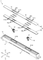
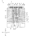
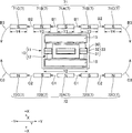
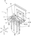
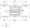
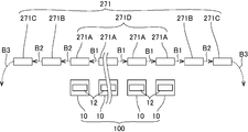
- FIG. 1 It is a perspective view of a magnetic sensor device to which the present invention is applied. It is a disassembled perspective view of the magnetic sensor apparatus of FIG. It is sectional drawing of the magnetic sensor apparatus of FIG. It is a top view which shows arrangement
- FIG. 1 is a perspective view of a magnetic sensor device 1 to which the present invention is applied.
- the magnetic sensor device 1 is mounted on a magnetic pattern detection device that detects a magnetic pattern from a sheet-like medium 2 such as banknotes and securities.
- the magnetic pattern detection device determines the authenticity or type of the medium 2 by comparing the signal (detection waveform) from the magnetic sensor device 1 with a reference waveform.
- the magnetic pattern detection device includes a medium transport mechanism (not shown) that transports the medium 2 in the first direction X, and a magnetic sensor that detects the magnetic pattern of the medium 2 when the transported medium 2 passes the magnetic reading position A.
- a device 1 is provided.
- the first direction X, the second direction Y, and the third direction Z are directions orthogonal to each other.
- the first direction X and the second direction Y are directions along the medium conveyance surface 3, and the third direction Z is a direction perpendicular to the medium conveyance surface 3.
- the first direction X is the medium conveyance direction.
- the magnetic pattern detection apparatus conveys the medium 2 to one side (+ X direction) and the other side ( ⁇ X direction) of the first direction X.
- the upper and lower directions of each member will be described with the third direction Z as the vertical direction, the direction from the medium transport surface 3 toward the medium 2 as the upper direction (+ Z direction), and the opposite direction as the lower direction ( ⁇ Z direction).
- FIG. 2 is an exploded perspective view of the magnetic sensor device 1
- FIG. 3 is a cross-sectional view of the magnetic sensor device 1 (cross-sectional view taken along line BB in FIG. 1).
- the magnetic sensor device 1 has a long shape in the second direction Y, and includes a medium transport surface 3 facing upward (+ Z direction).
- the magnetic sensor device 1 includes a sensor case 4 that is long in the second direction Y, a sensor unit 10 that is accommodated in the sensor case 4, a substrate 5 that is attached to the lower side of the bottom of the sensor case 4, and a medium that covers the sensor unit 10
- a cover plate 6 constituting the conveying surface 3, a plurality of magnets 7 held by the cover plate 6, and a magnetic shield case 8 disposed inside the sensor case 4 and covering the sensor unit 10 are provided.
- a signal processing circuit for processing a signal output from the sensor unit 10 is mounted on the substrate 5.
- the sensor case 4 is formed with a recess 41 extending in the second direction Y.
- the recess 41 opens upward (+ Z direction).
- magnetic shield cases 8 made of a magnetic metal such as permalloy are arranged at two locations separated in the second direction Y.
- Each magnetic shield case 8 accommodates a sensor unit 10.
- the magnetic shield case 8 includes a cylindrical portion 81 that surrounds both sides of the sensor unit 10 in the first direction X and both sides of the second direction Y, and a bottom plate portion 82 (located in the ⁇ Z direction) below the sensor unit 10. 3).
- the cover plate 6 is attached to the upper end of the sensor case 4 and closes the recess 41. Openings 61 are formed in the cover plate 6 at two locations overlapping the sensor unit 10.
- the cover plate 6 is a composite plate in which two stainless steel metal plates 62 and 63 are laminated.
- the surface of the metal plate 62 located above (+ Z direction) constitutes the medium transport surface 3.
- a rectangular recess 62a in which the magnet 7 is disposed is formed on the back surface (the surface on the ⁇ Z direction side) of the metal plate 62.
- a rectangular arrangement hole 63 a is formed in the metal plate 63 located below ( ⁇ Z direction) at a position overlapping the recess 62 a of the metal plate 62.
- the magnet 7 is inserted into the arrangement hole 63a and the recess 62a and is fixed to the cover plate 6 with an adhesive.
- the magnet 7 is a permanent magnet such as a ferrite or neodymium magnet, and is a magnetic pole in which the portion on the medium transport surface 3 side and the portion on the back side thereof are different.
- FIG. 4 is a plan view of the sensor unit 10 and the magnet 7.
- a first magnet row 71 is arranged on one side in the first direction X (+ X direction side) with respect to the sensor unit 10.
- the first magnet row 71 is composed of five magnets 7 arranged in the second direction Y at a constant pitch.
- a second magnet row 72 is arranged on the other side ( ⁇ X direction side) in the first direction X with respect to the sensor unit 10.
- the second magnet row 72 includes five magnets 7 arranged at a constant pitch in the second direction Y.
- the magnet 7 located at the center of the first magnet row 71 is a first magnetizing magnet 71A that magnetizes the medium 2 from one side of the first direction X (+ X direction) toward the sensor unit 10.
- the magnet 7 positioned at the center of the second magnet row 72 is a second magnetizing magnet 72A that magnetizes the medium 2 from the other side in the first direction X (the ⁇ X direction) toward the sensor unit 10. Details of the first magnet row 71 and the second magnet row 72 will be described later.
- FIG. 5 is a perspective view of the sensor unit 10 to which the conductive member 20 is attached as viewed from the lower side ( ⁇ Z direction side).
- the sensor unit 10 includes a substantially rectangular parallelepiped frame 11 and a magnetic sensor element 12 held by the frame 11. As shown in FIG. 3, the frame 11 is formed with a recess 13 that opens upward (in the + Z direction).
- the magnetic sensor element 12 is accommodated in the recess 13 and is fixed to the frame 11 by the resin 14 filled in the gap between the recess 13 and the magnetic sensor element 12 (see FIG. 3).
- Two wear-resistant plates 15 made of ceramic or the like are attached to the opening edge of the recess 13. The wear-resistant plates 15 are arranged on both sides of the magnetic sensor element 12 in the first direction X and extend in the second direction Y.
- a conductive member 20 is attached to the frame 11 of the sensor unit 10 from the outside.
- the conductive member 20 is a metal plate that includes an attachment portion 21, a leaf spring portion 22, and a connection portion 23.
- the attachment portion 21 is attached to the side surface 16 on the other side ( ⁇ X direction) of the frame 11 in the first direction X.
- the leaf spring portion 22 is bent at the lower end of the side surface 16 of the frame 11 and extends in the first direction X on the lower side ( ⁇ Z direction side) of the frame 11. Further, the connecting portion 23 extends linearly downward ( ⁇ Z direction) from the mounting portion 21.
- the magnetic sensor element 12 includes a first protection plate 30 and a second protection plate 31 made of a nonmagnetic material such as ceramics, and a sensor core 32 sandwiched therebetween.
- a core body 33 having a three-layer structure is provided.
- the sensor core 32 is made of a magnetic material such as ferrite, amorphous, permalloy, or silicon steel plate. As shown in FIG.
- the magnetic sensor element 12 includes an excitation coil 34 that generates a bias magnetic field and a detection coil 35 that detects the magnetic pattern of the medium 2.
- the magnetic sensor element 12 is disposed such that the thickness direction of the core body 33 coincides with the first direction X that is the medium conveyance direction.
- the width direction of the core body 33 (the left-right direction in FIG. 6A) coincides with the second direction Y.
- the core body 33 has a symmetrical shape with respect to the center in the second direction Y.
- the core body 33 includes a body portion 331 extending in the second direction Y (width direction) at the center in the third direction Z (height direction).
- Three protrusions protrude upward (+ Z direction) and downward ( ⁇ Z direction).
- the three protrusions protruding upward (+ Z direction) are an upper protrusion 332 located at the center and upper protrusions 334L and 334R located on both sides of the upper protrusion 332.
- the three protrusions protruding downward ( ⁇ Z direction) from the body part 331 are a lower protrusion 333 located in the center and lower protrusions 335L and 335R located on both sides of the lower protrusion 333. It is.
- the detection coil 35 is formed by winding a coil wire around the upper protrusion 332 of the core body 33 via a bobbin 37.
- the tip surface of the upper protrusion 332 on which the detection coil 35 is configured constitutes the sensor surface 12 a of the magnetic sensor element 12.
- the exciting coil 34 is formed by winding a coil wire around the bobbin 36 around the body portion 331 of the core body 33.
- One exciting coil 34 is disposed on each side of the upper protrusion 332 and the lower protrusion 333 located in the center of the core body 33 in the second direction Y (width direction). These two exciting coils 34 have the same number of turns of the coil wire, and the winding direction of the coil wire is opposite.
- the two exciting coils 34 are wound with one coil wire and connected in series.
- a gap G having a constant width is formed on both sides of the upper protrusion 332 and the lower protrusion 333 of the core body 33.
- the bobbin 36 around which the exciting coil 34 is wound includes four terminal pins 38.
- One end of the terminal pin 38 protrudes downward ( ⁇ Z direction) from the bobbin 36 and is electrically connected to a signal processing circuit provided on the substrate 5.
- a coil wire constituting the exciting coil 34 or the detection coil 35 is connected to the other end (upper end) of the terminal pin 38.
- the end of the first protection plate 30 is cut out by a certain dimension shorter than the end of the second protection plate 31. Yes. Therefore, an exposed portion 32a where the sensor core 32 is exposed by a certain dimension is provided at the lower end (end in the ⁇ Z direction) of the core body 33.
- the terminal pin 38 and the end of the core body 33 pass through the bottom opening 17 provided at the bottom of the frame 11. Projects downward (-Z direction).
- the leaf spring portion 22 of the conductive member 20 attached to the frame 11 is in elastic contact with the end portion of the core body 33 protruding from the bottom opening 17.
- the leaf spring portion 22 contacts the exposed portion 32a.
- the connecting portion 23 of the conductive member 20 and the four terminal pins 38 extend below the frame 11 ( ⁇ Z direction). As shown in FIG. 3, the connection portion 23 and the terminal pin 38 reach the substrate 5 through the penetration portion provided in the bottom portion of the sensor case 4 and the penetration portion formed in the bottom plate portion 82 of the magnetic shield case 8. It extends to the position to do.
- the tips of the four terminal pins 38 are respectively passed through through holes 51 formed in the substrate 5 and connected to a wiring pattern on the substrate 5 by solder (not shown).
- the connecting portion 23 of the conductive member 20 is passed through a through hole 52 formed in the substrate 5 and fixed by soldering or the like. As a result, the sensor core 32 is grounded via the substrate 5 and the conductive member 20.
- Magnetic pattern detection operation In the magnetic pattern detection device including the magnetic sensor device 1, when the medium 2 is transported to one side or the other side of the first direction X that is the medium transport direction, the medium 2 reaches the first position before reaching the magnetic reading position A. It is magnetized by the magnet for magnet 71A or the second magnet for magnet 72A. Then, the magnetized medium 2 passes through the magnetic reading position A by the magnetic sensor device 1.
- an alternating current is applied to the exciting coil 34 at a constant current, and a bias magnetic field indicated by an alternate long and short dash line in FIG. 6A is formed around the core body 33.
- a detection waveform of a differential signal with respect to the bias magnetic field and time is obtained from the detection coil 35.
- the shape, peak value, and bottom value of the detected waveform from the magnetic sensor element 12 vary depending on the type of magnetic ink used to form the magnetic pattern, the position of the magnetic pattern, and the density of the formed magnetic pattern. . Therefore, by comparing the detected waveform with a reference waveform stored and held in advance, the authenticity of the medium 2 and the type of the medium 2 can be determined.
- the magnetic sensor device 1 includes the first magnetizing magnet 71 ⁇ / b> A that magnetizes the medium 2 on one side in the first direction X (+ X direction) of the magnetic sensor element 12 provided in the sensor unit 10.
- a first magnet row 71 and a second magnet row 72 including a second magnetizing magnet 72A for magnetizing the medium 2 on the other side in the first direction X ( ⁇ X direction) of the magnetic sensor element 12 are provided.
- Each of the first magnet row 71 and the second magnet row 72 includes five magnets 7 whose magnetic pole directions are set so that different magnetic poles are alternately arranged in the second direction Y.
- the first magnet row 71 includes a first magnetic flux attracting magnet 71B arranged on both sides in the second direction Y of the first magnetizing magnet 71A, and these three magnets 7 (first The magnetic flux attracting magnet 71B, the first magnetizing magnet 71A, and the first magnetic flux attracting magnet 71B) are provided with second magnetic flux attracting magnets 71C disposed on both sides in the second direction Y.
- the magnetic pole on the medium conveyance surface 3 side of the first magnetic flux attracting magnet 71B is different from the magnetic pole on the medium conveyance surface 3 side of the first magnetizing magnet 71A and the second magnetic flux attraction magnet 71C.
- the second magnet row 72 includes a first magnetic flux attracting magnet 72B disposed on both sides in the second direction Y of the second magnetizing magnet 72A, and these three magnets 7 (first magnetic flux attracting magnet 72B, first magnet A second magnetic flux attracting magnet 72C disposed on both sides in the second direction Y of the second magnetizing magnet 72A and the first magnetic flux attracting magnet 72B).
- the magnetic pole on the medium transport surface 3 side of the first magnetic flux attracting magnet 72B is different from the magnetic pole on the medium transport surface 3 side of the second magnetizing magnet 72A and the second magnetic flux attracting magnet 72C.
- the first magnet row 71 and the second magnet row 72 are configured in the same way except that the magnetic poles of the magnet 7 at the position facing the first direction X are different magnetic poles.
- the first magnet row 71 and the second magnet row 72 are configured symmetrically with respect to the center in the second direction Y of the sensor unit 10. In the center of the sensor unit 10 in the first direction X, the sensor core 32 of the magnetic sensor element 12 is disposed.
- the first magnetizing magnet 71A and the second magnetizing magnet 72A have the same distance in the first direction X from the sensor core 32.
- the arrangement area Y1 of the first magnetizing magnet 71A and the second magnetizing magnet 72A in the second direction Y completely overlaps the arrangement area Y2 of the sensor core 32 in the second direction Y. Further, the arrangement area Y3 of the first magnetic flux attracting magnets 71B and 72B in the second direction Y partially overlaps the arrangement area Y2 of the sensor core 32 in the second direction Y. The arrangement area Y4 in the second direction Y of the second magnetic flux attracting magnets 71C and 72C is completely away from the arrangement area Y2 in the second direction Y of the sensor core 32.
- the magnetic pole of the first magnetic flux attracting magnet 71B is different from the magnetic pole of the first magnetizing magnet 71A. Accordingly, the magnetic flux B1 of the first magnetizing magnet 71A is attracted by the first magnetic flux attracting magnet 71B. Accordingly, the magnetic flux B1 of the first magnetizing magnet 71A is prevented from moving toward the vicinity of the sensor unit 10 by the first magnetic flux attracting magnet 71B. Therefore, when a disturbance magnetic field is applied, the possibility that the magnetic flux B1 of the first magnetizing magnet 71A is bent by the disturbance magnetic field and passes through the sensor core 32 is reduced.
- the first magnet row 71 includes a second magnetic flux attracting magnet 71C disposed on the opposite side of the first magnetizing magnet 71A with respect to the first magnetic flux attracting magnet 71B.
- the magnetic pole of the second magnetic flux attracting magnet 71C is different from the magnetic pole of the adjacent first magnetic flux attracting magnet 71B. Accordingly, the magnetic flux B2 of the first magnetic flux attracting magnet 71B is attracted by the second magnetic flux attracting magnet 71C.
- the second magnetic flux attracting magnet 71 ⁇ / b> C prevents the magnetic flux B ⁇ b> 2 of the first magnetic flux attracting magnet 71 ⁇ / b> B from moving toward the vicinity of the sensor unit 10. Therefore, when a disturbance magnetic field is applied, the possibility that the magnetic flux B2 of the first magnetic flux attracting magnet 71B is bent by the disturbance magnetic field and passes through the sensor core 32 is reduced.
- the magnet 7 is not arranged outside the second direction Y with respect to the second magnetic flux attracting magnet 71C, and the magnetic flux B3 of the second magnetic flux attracting magnet 71C is outside the second direction Y by another magnet. Will not be aspirated.
- the magnetic flux B3 of the second magnetic flux attracting magnet 71C passes through a position away from the sensor core 32. . Therefore, when a disturbance magnetic field is applied, even if the magnetic flux B3 of the second magnetic flux attracting magnet 71C is bent toward the sensor core 32, there is little possibility of passing through the sensor core 32.
- the magnetic flux C1 of the second magnetizing magnet 72A is attracted by the first magnetic flux attracting magnet 72B. Therefore, when a disturbance magnetic field is applied, the possibility that the magnetic flux C1 of the second magnetizing magnet 72A is bent and passes through the sensor core 32 is reduced.
- the magnetic flux C2 of the first magnetic flux attracting magnet 72B is attracted by the second magnetic flux attracting magnet 72C. Therefore, when a disturbance magnetic field is applied, the possibility that the magnetic flux C2 of the first magnetic flux attracting magnet 72B is bent and passes through the sensor core 32 is reduced.
- the magnetic flux C3 of the second magnetic flux attracting magnet 72C passes through a position away from the sensor core 32, even when a disturbance magnetic field is applied, the magnetic flux C3 of the second magnetic flux attracting magnet 72C is bent toward the sensor core 32 side. There is little risk of passing through the sensor core 32.
- the magnetic sensor device 1 of the present embodiment attracts the magnetic fluxes B1 and C1 of the first magnetizing magnet 71A and the second magnetizing magnet 72A with the first magnetism attracting magnets 71B and 72B. Therefore, the magnetic flux bent by the disturbance magnetic field in the vicinity of the magnetic sensor element 12 can be reduced. Thereby, the possibility that the magnetic flux passes through the sensor core 32 can be reduced. Accordingly, noise caused by the disturbance magnetic field can be reduced, and the detection accuracy of the magnetic sensor device 1 can be improved.
- the magnetic fluxes B2 and C2 of the first magnetic flux attracting magnets 71B and 72B are attracted by the second magnetic flux attracting magnets 71C and 72C.
- the possibility that the magnetic fluxes B2 and C2 of the first magnetic flux attracting magnets 71B and 72B are bent by the disturbance magnetic field and pass through the sensor core 32 can be reduced.
- the second magnetic flux attracting magnets 71C and 72C are separated from the sensor core 32, even if the magnetic fluxes B3 and C3 of the second magnetic flux attracting magnets 71C and 72C are bent by a disturbance magnetic field, the bent magnetic flux is There is little risk of passing 32. Accordingly, noise caused by the disturbance magnetic field can be reduced, and the detection accuracy of the magnetic sensor device 1 can be improved.
- the first magnetic flux attracting magnets 71B and 72B and the second magnetic flux attracting magnets 71C and 72C are arranged in the second direction Y with respect to the first magnetizing magnet 71A and the second magnetizing magnet 72A. Located on both sides. Therefore, the possibility that the magnetic flux bent by the disturbance magnetic field passes through the sensor core 32 not only on one side in the second direction Y but also on the other side with respect to the first magnetizing magnet 71A and the second magnetizing magnet 72A. be able to.
- the first magnet row 71 is arranged on one side in the first direction X with respect to the magnetic sensor element 12, and the second magnet row 72 is arranged on the other side.
- the medium 2 can be magnetized to read the magnetic pattern, and noise caused by the disturbance magnetic field can be reduced. Can be reduced. Therefore, it is possible to improve the detection accuracy when reading the magnetic pattern from the medium 2 conveyed to one side and the other side in the first direction X.
- FIG. 7 is a plan view showing the arrangement of the sensor unit and magnets of the first modification.
- the magnetic sensor device 1 of Modification 1 includes the same sensor unit 10 as that in the above embodiment, and includes a first magnet row 171 disposed on one side in the first direction X of the sensor unit 10 and the first direction of the sensor unit 10.
- a second magnet row 172 disposed on the other side of X is provided.
- the first magnet row 171 includes three magnets: a first magnetizing magnet 171A and a first magnetic flux attracting magnet 171B arranged on both sides in the second direction Y with respect to the first magnetizing magnet 171A.
- the magnetic pole on the medium conveying surface 3 side of the first magnetic flux attracting magnet 171B is different from the magnetic pole on the medium conveying surface 3 side of the first magnetizing magnet 171A.
- the first magnetizing magnet 171A of the first modification has a dimension in the second direction Y larger than that of the first magnetizing magnet 71A having the above-described configuration.
- the arrangement area Y5 in the second direction Y of the first magnetizing magnet 171A is substantially the same as the arrangement area for the three magnets in the above embodiment.
- the arrangement region Y5 in the second direction Y of the first magnetizing magnet 171A is not limited to the region shown in FIG. 7, and can be changed as appropriate.
- the second magnet row 172 includes a second magnetizing magnet 172A, and a first magnetic flux attracting magnet 172B disposed on both sides in the second direction Y with respect to the second magnetizing magnet 172A.
- the first magnet row 171 and the second magnet row 172 are configured identically except that the magnetic poles of the magnets located at positions facing the first direction X are different magnetic poles. That is, in the second magnetizing magnet 172A, the polarity of the magnetic pole on the medium transport surface 3 side is opposite to that of the first magnetizing magnet 171A. If the polarities of the magnetic pole of the first magnetizing magnet 171A and the magnetic pole of the second magnetizing magnet 172A are opposite, the transport direction can be determined from the output of the magnetic sensor element 12.
- the magnetic fluxes B1 and C1 of the first magnetizing magnet 171A and the second magnetizing magnet 172A are attracted by the first magnetic flux attracting magnets 171B and 172B.
- the possibility that the magnetic fluxes B1 and C1 bent by the disturbance magnetic field pass through the sensor core 32 can be reduced.
- the magnetic fluxes B2 and C2 of the first magnetic flux attracting magnets 171B and 172B are separated from the magnetic sensor element 12, even if the magnetic fluxes B2 and C2 are bent by the disturbance magnetic field, there is little possibility of passing through the sensor core 32. Therefore, noise caused by the disturbance magnetic field can be reduced.
- the first magnetic flux attracting magnet 171B also serves as the first magnetic flux attracting magnet 71B and the second magnetic flux attracting magnet 71C in the above-described form.
- the first magnetic flux attracting magnet 172B also serves as the first magnetic flux attracting magnet 72B and the second magnetic flux attracting magnet 72C of the above-described form. Therefore, the magnetic flux of the first magnetizing magnets 171A and 172A can be attracted in the same manner as in the above embodiment, and noise caused by the disturbance magnetic field can be reduced.
- one of the first magnet row 171 and the second magnet row 172 may be omitted. Moreover, in the said form, you may abbreviate
- column 72 may abbreviate
- the magnetic poles of the magnets facing the first direction X across the magnetic sensor element 12 may not be different magnetic poles. That is, the first magnet row 171 and the second magnet row 172 of Modification 1 may be configured identically. Further, the first magnet row 71 and the second magnet row 72 of the above-described form may be configured identically.
- FIG. 8 is a plan view showing the arrangement of the sensor unit and magnets of the second modification.
- the magnetic sensor device 1 of Modification 2 is a multi-channel type.
- a plurality of sensor units 10 having the same configuration as the above are arranged in the second direction Y at a constant pitch.
- Each sensor unit 10 includes a magnetic sensor element 12. That is, in the second modification, a magnetic sensor element array 100 in which a plurality of magnetic sensor elements 12 are arranged in the second direction Y at a constant pitch is provided.
- a first magnet row 271 is arranged on one side (+ X direction) in the first direction X of the magnetic sensor element row 100.
- the first magnet row 271 includes a first magnetizing magnet row 271D in which a plurality of first magnetizing magnets 271A are arranged at a constant pitch in the second direction Y, and a second direction Y of the first magnetizing magnet row 271D.
- Two first magnetic flux attracting magnets 271B disposed on both sides of the first magnetic flux attracting magnet 271B and two second magnetic flux attracting magnets 271B disposed on the opposite side of the first magnetizing magnet row 271D.
- a magnetic flux attracting magnet 271C is included.
- the number of first magnetizing magnets 271A constituting the first magnetizing magnet array 271D is the same as the number of magnetic sensor elements 12 included in the magnetic sensor element array 100.
- Each of the first magnetizing magnets 271 ⁇ / b> A is disposed on one side in the first direction X of the corresponding magnetic sensor element 12.
- the magnetic pole in the portion on the medium transport surface 3 side is different from the magnetic pole in the portion on the medium transport surface 3 side of the adjacent first magnetizing magnet 271A.
- the magnetic pole on the medium transport surface 3 side is different from the magnetic pole of the magnet adjacent in the second direction Y, respectively. That is, the magnetic poles of the first magnetizing magnet 271A located at both ends of the first magnetizing magnet row 271D are different from the magnetic poles of the adjacent first magnetic flux attracting magnets 271B.
- the magnetic pole of the first magnetic flux attracting magnet 271B is different from the magnetic pole of the second magnetic flux attracting magnet 271C adjacent on the opposite side to the first magnetizing magnet 271A.
- each of the plurality of first magnetizing magnets 271A attracts the magnetic flux to the adjacent first magnetizing magnet 271A or the first magnetic flux attracting magnet 271B. That is, each of the plurality of first magnetizing magnets 271A has a function of magnetizing the medium 2 and functions as a magnetic flux attracting magnet that attracts the magnetic flux B1 of the adjacent first magnetizing magnet 271A.
- the first magnetic flux attracting magnet 271B and the second magnetic flux attracting magnet 271C are respectively second in this order. They are lined up outside the direction Y.
- the magnetic flux B1 of the first magnetizing magnet 271A located at both ends of the first magnetizing magnet row 271D is attracted by the first magnetic flux attracting magnet 271B, and the magnetic flux B2 of the first magnetic flux attracting magnet 271B is the second.
- the magnetic flux is attracted by the magnetic flux attracting magnet 271C.
- the magnetic flux of the first magnetizing magnet 271A is less likely to be bent by the disturbance magnetic field and pass through the sensor core 32.
- the magnetic flux bent by the disturbance magnetic field passes through the sensor core 32 of the magnetic sensor element 12. Therefore, the detection accuracy of the magnetic sensor elements 12 constituting the magnetic sensor element array 100 is less likely to be lowered by the disturbance magnetic field.
- the second magnet row may be arranged on the other side of the sensor unit 10 in the first direction X.
- the second magnet array includes a second magnetizing magnet array in which a plurality of second magnetizing magnets are arranged so that different magnetic poles are alternately arranged in the second direction Y, and a second magnetizing magnet.
- a first magnetic flux attracting magnet and a second magnetic flux attracting magnet disposed on both sides of the magnet array in the second direction Y.
- the second magnetic flux attracting magnet 271C may be omitted, and only the first magnetic flux attracting magnet 271B may be disposed at both ends of the first magnetizing magnet row 271D.
- FIG. 9 is a plan view showing the arrangement of the sensor unit and magnets of the third modification.
- the magnetic sensor device 1 of Modification 3 is a multi-channel type.
- a plurality of sensor units 10 that are the same as those in the above embodiment are arranged in the second direction Y at a constant pitch.
- Each sensor unit 10 includes a magnetic sensor element 12.
- a first magnet array 371 is arranged on one side (+ X direction) of the first direction X of the magnetic sensor element array 100 in which the plurality of magnetic sensor elements 12 are arranged at a constant pitch in the second direction Y.
- the first magnet row 371 is configured by alternately arranging the first magnetizing magnets 371A and the first magnetic flux attracting magnets 371B in the second direction Y.
- Each of the plurality of first magnetizing magnets 371A included in the first magnet row 371 magnetizes the medium toward the corresponding magnetic sensor element 12.
- First magnetic flux attracting magnets 371B are disposed at both ends of the first magnet row 371, respectively.
- a second magnet row 372 is arranged on the other side ( ⁇ X direction) of the first direction X of the magnetic sensor element row 100.
- the second magnet row 372 is configured by alternately arranging second magnetizing magnets 372A and second magnetic flux attracting magnets 372B in the second direction Y.
- Each of the plurality of second magnetizing magnets 372A included in the second magnet row 372 magnetizes the medium toward the corresponding magnetic sensor element 12.
- a second magnetic flux attracting magnet 372B is disposed at each end of the second magnet row 372.
- each of the plurality of first magnetizing magnets 371A attracts the magnetic flux B1 by the adjacent first magnetic flux attracting magnet 371B. Further, each of the plurality of second magnetizing magnets 372A is attracted by the adjacent second magnetic flux attracting magnet 372B. Accordingly, similarly to the second modification, the magnetic fluxes B1 and C1 of the first magnetizing magnet 271A and the second magnetizing magnet 372A are less likely to be bent by the disturbance magnetic field and pass through the sensor core 32. Further, the first magnetic flux attracting magnet 371B is located at both ends of the first magnet row 371, and the second magnetic flux attracting magnet 372B is located at both ends of the second magnet row 372.
- the magnetic fluxes B1 and C1 bent by the disturbance magnetic field are less likely to pass through the sensor core 32. Furthermore, the magnetic flux of the first magnetic flux attracting magnet 371B is attracted by the first magnetizing magnet 371A located next to it, and the magnetic flux of the second magnetic flux attracting magnet 372B is located next to it. It is attracted by the magnet 372A. That is, the first magnetizing magnet 371A and the second magnetizing magnet 372A also function as magnetic flux attracting magnets that attract the magnetic fluxes of the adjacent first magnetic flux attracting magnets 371B and 372B. Therefore, the detection accuracy of the magnetic sensor elements 12 constituting the magnetic sensor element array 100 is less likely to be lowered by the disturbance magnetic field.
- one of the first magnet row 371 and the second magnet row 372 may be omitted.
- a second magnetic flux attracting magnet may be added to one end or both ends of the first magnet row 371 and the second magnet row 372.
- the magnetic flux attracting magnet located next to the magnetizing magnet functions as a first magnetic flux attracting magnet that attracts the magnetic flux of the magnetizing magnet, and with respect to the first magnetic flux attracting magnet.
- the magnetic flux attracting magnet located on the opposite side of the magnetizing magnet functions as a second magnetic flux attracting magnet that attracts the magnetic flux of the first magnetic flux attracting magnet. Therefore, the detection accuracy of the magnetic sensor elements constituting the magnetic sensor element array 100 is less likely to be lowered by the disturbance magnetic field.
- the magnetizing magnet, the first magnetic flux attracting magnet, and the second magnetic flux attracting magnet are arranged symmetrically with respect to the center of the sensor unit 10 in the second direction Y.
- the magnet and the second magnetic flux attracting magnet may be arranged only on one side or the other side in the second direction Y with respect to the magnetizing magnet.
- SYMBOLS 1 Magnetic sensor apparatus, 2 ... Medium, 3 ... Medium conveyance surface, 4 ... Sensor case, 5 ... Board
- second magnetizing magnet 372B ... first magnetic flux attracting Magnet, A ... magnetic reading position, B1 ... magnetic flux of the first magnetizing magnet, B2 ... magnetic flux of the first magnetic flux attracting magnet, B3 ... magnetic flux of the second magnetic flux attracting magnet, C1 ... second magnetizing magnet.
Landscapes
- Physics & Mathematics (AREA)
- General Physics & Mathematics (AREA)
- Condensed Matter Physics & Semiconductors (AREA)
- Inspection Of Paper Currency And Valuable Securities (AREA)
- Measuring Magnetic Variables (AREA)
Abstract
外乱磁界によって曲げられた磁束がセンサコアを通過することによる検出精度の低下を抑制すること。磁気センサ装置1は、磁気センサ素子12に対して第1方向Xの一方側に配置される第1マグネット列71と、他方側に配置される第2マグネット列72を備える。第1マグネット列71は、媒体2を着磁する第1着磁用マグネット71Aと第2方向Yに隣り合う第1磁束吸引用マグネット72Bと、第1磁束吸引用マグネット72Bと第2方向Yに隣り合う第2磁束吸引用マグネット71Cを備える。第1磁束吸引用マグネット72Bと第2磁束吸引用マグネット71Cは隣り合うマグネットと異なる磁極を備え、隣り合うマグネットの磁束を吸引する。従って、磁気センサ素子12の近傍の磁束が外乱磁界によって曲げられてセンサコア32を通るおそれが少ないので、外乱磁界に起因するノイズを低減できる。
Description
本発明は、媒体の磁気パターンを検出する磁気センサ装置に関する。
従来から、着磁マグネットにより媒体に着磁を行い、着磁された媒体の磁気パターンを読み取る磁気センサ装置が知られている。特許文献1に記載の磁気センサ装置は、バイアス磁界を発生させる励磁コイルと、磁気パターンを検出する検出コイルを備えた磁気センサ素子を有する。磁気センサ素子は、アモルファスあるいはパーマロイからなる板状のセンサコアからなるコア体を備える。コア体にボビンを介してコイル線を巻き回すことにより、励磁コイルおよび検出コイルが形成される。
磁気センサ装置において、着磁用マグネットは、磁気センサ素子を通過する前の媒体の通過位置に配置される。例えば、特許文献1では、磁気センサ素子に対して媒体搬送方向の一方側に第1着磁用マグネットが配置され、他方側に第2着磁用マグネットが配置される。
特許文献1の磁気センサ装置は、複数の磁気センサ素子を媒体搬送方向と直交する方向に一列に配列した多チャンネル型の磁気センサ装置である。従って、第1着磁用マグネットと第2着磁用マグネットは、それぞれ、磁気センサ素子に対して媒体搬送方向の一方側と他方側において、磁気センサ素子と同じ数が一列に配列される。第1着磁用マグネットと第2着磁用マグネットの列は、それぞれ、異なる磁極を交互に配置して構成される。
ここで、1チャンネル型の磁気センサ装置の場合、1つの磁気センサ素子に対して、少なくとも、媒体搬送方向の一方側に1つの着磁用マグネットが配置される。このような配置において、磁気センサ素子に外乱磁界が加わると、着磁用マグネットの磁束のうち、磁気センサ素子から離れた位置を通る磁束が曲げられて磁気センサ素子のセンサコアを通過するおそれがある。着磁用マグネットの磁束がセンサコアを通過すると磁気センサ素子の信号にノイズが加わり、検出精度が低下する。
また、多チャンネル型の磁気センサ装置であっても、上記の1チャンネル型の磁気センサ装置と同様に、着磁用マグネットの磁束が外乱磁界によって磁気センサ側へ曲げられてセンサコアを通過するおそれがある。特に、列の端に位置する着磁用マグネットの磁束は、他のマグネットによって吸引されないので、外乱磁界によって磁気センサ素子側へ曲げられてセンサコアを磁束が通過するおそれがある。従って、磁気センサ素子の信号にノイズが加わり、検出精度が低下するおそれがある。
本発明の課題は、このような点に鑑みて、外乱磁界によって曲げられた磁束がセンサコアを通過することによる磁気センサ装置の検出精度の低下を抑制することにある。
上記の課題を解決するために、本発明の磁気センサ装置は、磁気センサ素子と、前記磁気センサ素子へ向かう媒体を着磁する着磁用マグネットと、少なくとも1つの磁束吸引用マグネットと、を有し、前記着磁用マグネットおよび前記磁束吸引用マグネットは、媒体搬送方向と交差する方向に並んでおり、前記着磁用マグネットの磁極は、前記着磁用マグネットと隣り合う前記磁束吸引用マグネットの磁極と異なることを特徴とする。
本発明は、このように、着磁用マグネットの隣に少なくとも1つの磁束吸引用マグネットを配置する。これにより、着磁用マグネットから発生する磁束を磁束吸引用マグネットで吸引する。このようにすると、磁気センサ素子の近傍で外乱磁界によって曲げられる磁束を少なくすることができる。これにより、磁気センサ素子のセンサコアを磁束が通るおそれを少なくすることができる。従って、外乱磁界に起因するノイズを低減させることができ、磁気センサ装置の検出精度を向上させることができる。
本発明において、前記磁束吸引用マグネットは、前記着磁用マグネットと隣り合う第1磁束吸引用マグネット、および、前記第1磁束吸引用マグネットに対して前記着磁用マグネットと反対の側で隣り合う第2磁束吸引用マグネットを含み、前記第2磁束吸引用マグネットの磁極は、前記第1磁束吸引用マグネットの磁極と異なることが望ましい。このようにすると、着磁用マグネットの磁束が吸引されるだけでなく、第1磁束吸引用マグネットの磁束も第2磁束吸引用マグネットによって吸引される。従って、第1磁束吸引用マグネットの磁束が外乱磁界によって曲げられてセンサコアを通るおそれは少ない。そして、第2磁束吸引用マグネットはセンサコアから離れているので、第2磁束吸引用マグネットの磁束が外乱磁界によって曲げられたとしても、曲げられた磁束がセンサコアを通るおそれは少ない。従って、外乱磁界に起因するノイズを低減させることができる。
本発明において、前記着磁用マグネットおよび前記磁束吸引用マグネットは、前記磁気センサ素子に対して前記媒体搬送方向の一方側および他方側に配置されることが望ましい。このようにすると、媒体搬送方向の一方側と他方側のいずれの方向へ媒体を搬送する場合においても、外乱磁界に起因するノイズを低減させることができる。従って、媒体搬送方向の一方側および他方側へ搬送される媒体から磁気パターンを読み取る際の磁気センサ装置の検出精度を向上させることができる。
本発明において、前記磁束吸引用マグネットは、前記着磁用マグネットに対して前記媒体搬送方向と交差する方向の両側に配置されることが望ましい。このようにすると、着磁用マグネットに対して媒体搬送方向と交差する方向の一方側だけでなく他方側においても、外乱磁界によって曲げられる磁束がセンサコアを通るおそれを少なくすることができる。
本発明において、前記媒体搬送方向と交差する方向に一列に並ぶ複数の前記磁気センサ素子と、前記複数の前記磁気センサ素子に対応する複数の前記着磁用マグネット、および、少なくとも1つの前記磁束吸引用マグネットが前記媒体搬送方向と交差する方向に一列に並ぶマグネット列と、を有し、前記複数の前記着磁用マグネットのそれぞれの磁極は、隣り合う前記磁束吸引用マグネットの磁極、もしくは、隣り合う前記着磁用マグネットの磁極と異なることが望ましい。このようにすると、着磁用マグネットのそれぞれが、隣り合う着磁用マグネットもしくは磁束吸引用マグネットと互いに磁束を吸引し合う。従って、多チャンネル型の磁気センサ装置において、磁気センサ素子の近傍で外乱磁界によって曲げられる磁束を少なくすることができる。従って、多チャンネル型の磁気センサ装置の検出精度を向上させることができる。
本発明において、前記マグネット列の端に前記磁束吸引用マグネットが位配置されることが望ましい。このようにすると、多チャンネル型の磁気センサ装置において、列の端に位置する磁気センサ素子へ向かう媒体を着磁する着磁用マグネットの磁束を磁束吸引用マグネットによって吸引できる。従って、列の端に位置する磁気センサ素子に対しても、外乱磁界によって曲げられた磁束がセンサコアを通るおそれを少なくすることができる。従って、多チャンネル型の磁気センサ装置において、列の端に位置する磁気センサ素子の検出精度を向上させることができる。
本発明において、前記マグネット列は、前記着磁用マグネットと前記磁束吸引用マグネットが交互に並んだ列である。このようにすると、着磁用マグネットのそれぞれは、両側に位置する磁束吸引用マグネットによって磁束が吸引される。従って、磁気センサ素子の近傍で外乱磁界によって曲げられる磁束を少なくすることができる。従って、多チャンネル型の磁気センサ装置の検出精度を向上させることができる。
本発明によれば、着磁用マグネットの隣に少なくとも1つの磁束吸引用マグネットを配置することにより、着磁用マグネットから発生する磁束を磁束吸引用マグネットで吸引する。これにより、磁気センサ素子の近傍で外乱磁界によって曲げられる磁束を少なくすることができる。従って、外乱磁界によって曲げられる磁束が磁気センサ素子のセンサコアを通るおそれを少なくすることができる。よって、外乱磁界に起因するノイズを低減させることができ、磁気センサ装置の検出精度を向上させることができる。
以下に、図面を参照して、本発明を適用した磁気センサ装置を説明する。
(全体構成)
図1は本発明を適用した磁気センサ装置1の斜視図である。磁気センサ装置1は、銀行券、有価証券等のシート状の媒体2から磁気パターンを検出する磁気パターン検出装置に搭載される。磁気パターン検出装置は、磁気センサ装置1からの信号(検出波形)をリファレンス波形と照合することによって、媒体2の真偽判定や種類を判別する。磁気パターン検出装置は、媒体2を第1方向Xに搬送する媒体搬送機構(図示省略)と、搬送される媒体2が磁気読み取り位置Aを通過する際に媒体2の磁気パターンを検出する磁気センサ装置1を備える。
図1は本発明を適用した磁気センサ装置1の斜視図である。磁気センサ装置1は、銀行券、有価証券等のシート状の媒体2から磁気パターンを検出する磁気パターン検出装置に搭載される。磁気パターン検出装置は、磁気センサ装置1からの信号(検出波形)をリファレンス波形と照合することによって、媒体2の真偽判定や種類を判別する。磁気パターン検出装置は、媒体2を第1方向Xに搬送する媒体搬送機構(図示省略)と、搬送される媒体2が磁気読み取り位置Aを通過する際に媒体2の磁気パターンを検出する磁気センサ装置1を備える。
本明細書において、第1方向X、第2方向Y、第3方向Zは互いに直交する方向である。第1方向Xと第2方向Yは媒体搬送面3に沿う方向であり、第3方向Zは媒体搬送面3に対して垂直な方向である。第1方向Xは媒体搬送方向である。磁気パターン検出装置は、媒体2を第1方向Xの一方側(+X方向)および他方側(-X方向)へ搬送する。以下、第3方向Zを上下方向とし、媒体搬送面3から媒体2へ向かう方向を上方(+Z方向)、その逆方向を下方(-Z方向)として各部材の上下を説明する。
図2は磁気センサ装置1の分解斜視図であり、図3は磁気センサ装置1の断面図(図1のB-B断面図)である。図1に示すように、磁気センサ装置1は第2方向Yに長い形状をしており、上方(+Z方向)を向く媒体搬送面3を備える。磁気センサ装置1は、第2方向Yに長いセンサケース4と、センサケース4に収容されるセンサユニット10と、センサケース4の底部の下側に取り付けられる基板5と、センサユニット10を覆い媒体搬送面3を構成するカバー板6と、カバー板6に保持される複数のマグネット7と、センサケース4の内側に配置されセンサユニット10を覆う磁気シールドケース8を備える。基板5には、センサユニット10から出力される信号を処理する信号処理回路が実装される。
図2に示すように、センサケース4には第2方向Yに延在する凹部41が形成される。
凹部41は上方(+Z方向)に開口する。凹部41には、パーマロイなどの磁性金属からなる磁気シールドケース8が第2方向Yに離れた2箇所に配置される。各磁気シールドケース8にはセンサユニット10が収容される。磁気シールドケース8は、センサユニット10の第1方向Xの両側および第2方向Yの両側を囲む筒状部81と、センサユニット10の下側(-Z方向)に配置される底板部82(図3参照)を備える。
凹部41は上方(+Z方向)に開口する。凹部41には、パーマロイなどの磁性金属からなる磁気シールドケース8が第2方向Yに離れた2箇所に配置される。各磁気シールドケース8にはセンサユニット10が収容される。磁気シールドケース8は、センサユニット10の第1方向Xの両側および第2方向Yの両側を囲む筒状部81と、センサユニット10の下側(-Z方向)に配置される底板部82(図3参照)を備える。
図1に示すように、カバー板6はセンサケース4の上端に取り付けられ、凹部41を塞いでいる。カバー板6には、センサユニット10と重なる2箇所に開口部61が形成される。図2に示すように、カバー板6は、2枚のステンレス鋼製の金属板62、63を積層した複合板である。上方(+Z方向)に位置する金属板62の表面は、媒体搬送面3を構成する。金属板62の裏面(-Z方向側の面)には、マグネット7を配置する矩形の凹部62aが形成される。また、下方(-Z方向)に位置する金属板63には、金属板62の凹部62aと重なる位置に矩形の配置孔63aが形成される。マグネット7は、配置孔63aおよび凹部62aに挿入され、接着剤によりカバー板6に固定される。マグネット7はフェライトやネオジウム磁石等の永久磁石であり、媒体搬送面3側の部位とその裏側の部位とが異なる磁極である。
図4はセンサユニット10およびマグネット7の平面図である。センサユニット10に対して第1方向Xの一方側(+X方向側)には第1マグネット列71が配置される。第1マグネット列71は、第2方向Yに一定ピッチで並ぶ5個のマグネット7からなる。また、センサユニット10に対して第1方向Xの他方側(-X方向側)には第2マグネット列72が配置される。第2マグネット列72は、第2方向Yに一定ピッチで並ぶ5個のマグネット7からなる。第1マグネット列71の中央に位置するマグネット7は、第1方向Xの一方側(+X方向)からセンサユニット10へ向かう媒体2を着磁する第1着磁用マグネット71Aである。また、第2マグネット列72の中央に位置するマグネット7は、第1方向Xの他方側(-X方向)からセンサユニット10へ向かう媒体2を着磁する第2着磁用マグネット72Aである。第1マグネット列71と第2マグネット列72の詳細については後述する。
(センサユニット)
図5は導電部材20を取り付けたセンサユニット10を下側(-Z方向側)から見た斜視図である。センサユニット10は、略直方体状のフレーム11と、フレーム11に保持される磁気センサ素子12を備える。図3に示すように、フレーム11には、上方(+Z方向)に開口する凹部13が形成される。磁気センサ素子12は凹部13に収容され、凹部13と磁気センサ素子12との隙間に充填される樹脂14によってフレーム11に固定される(図3参照)。凹部13の開口縁にはセラミック等からなる2枚の耐摩耗板15が取り付けられる。耐摩耗板15は、磁気センサ素子12の第1方向Xの両側に配置され、第2方向Yに延在する。
図5は導電部材20を取り付けたセンサユニット10を下側(-Z方向側)から見た斜視図である。センサユニット10は、略直方体状のフレーム11と、フレーム11に保持される磁気センサ素子12を備える。図3に示すように、フレーム11には、上方(+Z方向)に開口する凹部13が形成される。磁気センサ素子12は凹部13に収容され、凹部13と磁気センサ素子12との隙間に充填される樹脂14によってフレーム11に固定される(図3参照)。凹部13の開口縁にはセラミック等からなる2枚の耐摩耗板15が取り付けられる。耐摩耗板15は、磁気センサ素子12の第1方向Xの両側に配置され、第2方向Yに延在する。
図5に示すように、センサユニット10のフレーム11には外側から導電部材20が取り付けられる。導電部材20は、取付部21、板バネ部22、および接続部23を備えた金属板である。取付部21は、フレーム11の第1方向Xの他方側(-X方向)の側面16に取り付けられる。板バネ部22はフレーム11の側面16の下端において屈曲され、フレーム11の下側(-Z方向側)で第1方向Xに延びている。また、接続部23は取付部21から下方(-Z方向)へ直線状に延びている。
(磁気センサ素子)
図6(a)は磁気センサ素子12の正面図であり、図6(b)は磁気センサ素子12の側面図であり、図6(c)は磁気センサ素子12の上面図である。図6(b)、(c)に示すように、磁気センサ素子12は、セラミックス等の非磁性体からなる第1保護板30、第2保護板31と、その間に挟まれたセンサコア32からなる三層構造のコア体33を備える。センサコア32はフェライト、アモルファス、パーマロイ、珪素鋼板等の磁性体から形成される。また、図6(a)に示すように、磁気センサ素子12は、バイアス磁界を発生させる励磁コイル34と、媒体2の磁気パターンを検出する検出コイル35を備える。磁気センサ素子12は、コア体33の厚さ方向が媒体搬送方向である第1方向Xと一致するように配置される。コア体33の幅方向(図6(a)の左右方向)は第2方向Yと一致する。コア体33は、第2方向Yの中央を基準として左右対称な形状である。
図6(a)は磁気センサ素子12の正面図であり、図6(b)は磁気センサ素子12の側面図であり、図6(c)は磁気センサ素子12の上面図である。図6(b)、(c)に示すように、磁気センサ素子12は、セラミックス等の非磁性体からなる第1保護板30、第2保護板31と、その間に挟まれたセンサコア32からなる三層構造のコア体33を備える。センサコア32はフェライト、アモルファス、パーマロイ、珪素鋼板等の磁性体から形成される。また、図6(a)に示すように、磁気センサ素子12は、バイアス磁界を発生させる励磁コイル34と、媒体2の磁気パターンを検出する検出コイル35を備える。磁気センサ素子12は、コア体33の厚さ方向が媒体搬送方向である第1方向Xと一致するように配置される。コア体33の幅方向(図6(a)の左右方向)は第2方向Yと一致する。コア体33は、第2方向Yの中央を基準として左右対称な形状である。
図6(a)に示すように、コア体33は、第3方向Z(高さ方向)の中央において第2方向Y(幅方向)に延在する胴部331を備えており、胴部331から上方(+Z方向)および下方(-Z方向)にそれぞれ3本ずつ突部が突出する。上方(+Z方向)に突出する3本の突部は、中央に位置する上側突部332と、上側突部332の両側に位置する上側突部334L、334Rである。また、胴部331から下方(-Z方向)に突出する3本の突部は、中央に位置する下側突部333と、下側突部333の両側に位置する下側突部335L、335Rである。
検出コイル35は、コア体33の上側突部332にボビン37を介してコイル線を巻き回して形成される。検出コイル35が構成された上側突部332の先端面は、磁気センサ素子12のセンサ面12aを構成する。励磁コイル34は、コア体33の胴部331にボビン36を介してコイル線を巻き回して形成される。励磁コイル34は、コア体33の第2方向Y(幅方向)の中央に位置する上側突部332と下側突部333の両側にそれぞれ、1つずつ配置される。これら2つの励磁コイル34はコイル線の巻き数が同一で、且つ、コイル線の巻き方向が逆向きである。2つの励磁コイル34は、1本のコイル線で巻かれており、直列に接続される。コア体33の上側突部332と下側突部333の両側には、それぞれ一定幅のギャップGが形成される。励磁コイル34に電流を流すと、4箇所のギャップGの周囲に設けられたU字型の開磁路を通る磁束が生じる。その結果、図6(a)において一点鎖線で示すバイアス磁界が形成される。
励磁コイル34が巻き回されるボビン36は、4本の端子ピン38を備える。端子ピン38の一端はボビン36から下方(-Z方向)へ突出し、基板5に設けられた信号処理回路と電気的に接続される。一方、端子ピン38の他端(上端)には、励磁コイル34あるいは検出コイル35を構成するコイル線が接続される。
図6(b)に示すように、コア体33の下端(-Z方向の端部)において、第1保護板30の端部は第2保護板31の端部より一定寸法短く切り欠かれている。従って、コア体33の下端(-Z方向の端部)には、センサコア32が一定寸法だけ露出した露出部32aが設けられている。
図3、図5に示すように、磁気センサ素子12がフレーム11に保持された状態では、端子ピン38およびコア体33の端部は、フレーム11の底部に設けられた底部開口17を通って下方(-Z方向)へ突出する。フレーム11に取り付けられた導電部材20の板バネ部22は、底部開口17から突出するコア体33の端部と弾性接触する。上述したように、コア体33の端部にはセンサコア32の露出部32aが設けられているため、板バネ部22は露出部32aと接触する。
導電部材20の接続部23と4本の端子ピン38は、フレーム11の下方(-Z方向)へ延びている。図3に示すように、接続部23と端子ピン38は、センサケース4の底部に設けられた貫通部、および磁気シールドケース8の底板部82に形成された貫通部を通り、基板5に到達する位置まで延びている。4本の端子ピン38の先端は、それぞれ、基板5に形成されたスルーホール51に通され、図示しない半田によって基板5上の配線パターンに接続される。また、導電部材20の接続部23は基板5に形成されたスルーホール52に通され、半田等によって固定される。これにより、基板5および導電部材20を介してセンサコア32が接地される。
(磁気パターン検出動作)
磁気センサ装置1を備える磁気パターン検出装置において、媒体2が媒体搬送方向である第1方向Xの一方側もしくは他方側に搬送されると、媒体2は磁気読み取り位置Aに至る前に第1着磁用マグネット71Aあるいは第2着磁用マグネット72Aにより着磁される。そして、着磁された媒体2が磁気センサ装置1による磁気読み取り位置Aを通過する。
磁気センサ装置1を備える磁気パターン検出装置において、媒体2が媒体搬送方向である第1方向Xの一方側もしくは他方側に搬送されると、媒体2は磁気読み取り位置Aに至る前に第1着磁用マグネット71Aあるいは第2着磁用マグネット72Aにより着磁される。そして、着磁された媒体2が磁気センサ装置1による磁気読み取り位置Aを通過する。
磁気センサ装置1では、励磁コイル34に交番電流が定電流で印加され、コア体33の周りには、図6(a)において一点鎖線で示すバイアス磁界が形成される。媒体2が磁気読み取り位置Aを通過すると、検出コイル35からは、バイアス磁界および時間に対する微分的な信号の検出波形が得られる。
磁気センサ素子12からの検出波形の形状、ピーク値およびボトム値は、磁気パターンの形成に用いられている磁気インクの種類、磁気パターンの位置、および、形成されている磁気パターンの濃淡によって変化する。従って、かかる検出波形を、予め記憶保持しているリファレンス波形と照合することにより、媒体2の真偽判定および媒体2の種類の判別を行うことができる。
(マグネット列)
上述したように、磁気センサ装置1は、センサユニット10に設けられた磁気センサ素子12の第1方向Xの一方側(+X方向)で媒体2を着磁する第1着磁用マグネット71Aを含む第1マグネット列71と、磁気センサ素子12の第1方向Xの他方側(-X方向)で媒体2を着磁する第2着磁用マグネット72Aを含む第2マグネット列72を備える。第1マグネット列71と第2マグネット列72は、それぞれ、第2方向Yに交互に異なる磁極が配置されるように磁極の向きを設定した5個のマグネット7を備える。
上述したように、磁気センサ装置1は、センサユニット10に設けられた磁気センサ素子12の第1方向Xの一方側(+X方向)で媒体2を着磁する第1着磁用マグネット71Aを含む第1マグネット列71と、磁気センサ素子12の第1方向Xの他方側(-X方向)で媒体2を着磁する第2着磁用マグネット72Aを含む第2マグネット列72を備える。第1マグネット列71と第2マグネット列72は、それぞれ、第2方向Yに交互に異なる磁極が配置されるように磁極の向きを設定した5個のマグネット7を備える。
図4に示すように、第1マグネット列71は、第1着磁用マグネット71Aの第2方向Yの両側に配置された第1磁束吸引用マグネット71Bと、これら3個のマグネット7(第1磁束吸引用マグネット71B、第1着磁用マグネット71A、第1磁束吸引用マグネット71B)の第2方向Yの両側に配置された第2磁束吸引用マグネット71Cを備える。第1磁束吸引用マグネット71Bの媒体搬送面3側の磁極は、第1着磁用マグネット71Aおよび第2磁束吸引用マグネット71Cの媒体搬送面3側の磁極と異なる磁極である。
第2マグネット列72は、第2着磁用マグネット72Aの第2方向Yの両側に配置された第1磁束吸引用マグネット72Bと、これら3個のマグネット7(第1磁束吸引用マグネット72B、第2着磁用マグネット72A、第1磁束吸引用マグネット72B)の第2方向Yの両側に配置された第2磁束吸引用マグネット72Cを備える。第1磁束吸引用マグネット72Bの媒体搬送面3側の磁極は、第2着磁用マグネット72Aおよび第2磁束吸引用マグネット72Cの媒体搬送面3側の磁極と異なる磁極である。
第1マグネット列71と第2マグネット列72は、第1方向Xに対向する位置にあるマグネット7の磁極が異なる磁極であることを除き、同一に構成される。第1マグネット列71と第2マグネット列72は、センサユニット10の第2方向Yの中央を基準として対称に構成される。センサユニット10の第1方向Xの中央には、磁気センサ素子12のセンサコア32が配置される。第1着磁用マグネット71Aと第2着磁用マグネット72Aは、センサコア32からの第1方向Xの距離が同一である。
図4に示すように、第1着磁用マグネット71Aおよび第2着磁用マグネット72Aの第2方向Yの配置領域Y1は、センサコア32の第2方向Yの配置領域Y2と完全に重なる。また、第1磁束吸引用マグネット71B、72Bの第2方向Yの配置領域Y3は、センサコア32の第2方向Yの配置領域Y2と一部が重なる。そして、第2磁束吸引用マグネット71C、72Cの第2方向Yの配置領域Y4は、センサコア32の第2方向Yの配置領域Y2から完全に外れた位置にある。
第1マグネット列71において、第1磁束吸引用マグネット71Bの磁極は第1着磁用マグネット71Aの磁極と異なる。従って、第1着磁用マグネット71Aの磁束B1は第1磁束吸引用マグネット71Bによって吸引される。これにより、第1着磁用マグネット71Aの磁束B1がセンサユニット10の近傍へ向かうことが第1磁束吸引用マグネット71Bによって妨げられる。従って、外乱磁界が加わったとき、第1着磁用マグネット71Aの磁束B1が外乱磁界によって曲げられてセンサコア32を通るおそれが低減される。
また、第1マグネット列71は、第1磁束吸引用マグネット71Bに対して第1着磁用マグネット71Aと逆の側に配置された第2磁束吸引用マグネット71Cを備える。そして、第2磁束吸引用マグネット71Cの磁極は、隣り合う第1磁束吸引用マグネット71Bの磁極と異なる。従って、第1磁束吸引用マグネット71Bの磁束B2は第2磁束吸引用マグネット71Cによって吸引される。これにより、第1磁束吸引用マグネット71Bの磁束B2がセンサユニット10の近傍へ向かうことが第2磁束吸引用マグネット71Cによって妨げられる。従って、外乱磁界が加わったとき、第1磁束吸引用マグネット71Bの磁束B2が外乱磁界によって曲げられてセンサコア32を通るおそれが低減される。
一方、第2磁束吸引用マグネット71Cに対して第2方向Yの外側にはマグネット7は配置されておらず、第2磁束吸引用マグネット71Cの磁束B3は他のマグネットによって第2方向Yの外側へ吸引されることはない。しかしながら、第2磁束吸引用マグネット71Cはセンサコア32の第2方向Yの配置領域Y2から完全に外れた位置にあるため、第2磁束吸引用マグネット71Cの磁束B3はセンサコア32から離れた位置を通る。従って、外乱磁界が加わったときに、第2磁束吸引用マグネット71Cの磁束B3がセンサコア32側へ曲げられたとしてもセンサコア32を通るおそれは少ない。
同様に、第2マグネット列72においても、第2着磁用マグネット72Aの磁束C1は第1磁束吸引用マグネット72Bによって吸引される。従って、外乱磁界が加わったとき、第2着磁用マグネット72Aの磁束C1が曲げられてセンサコア32を通るおそれが低減される。また、第1磁束吸引用マグネット72Bの磁束C2は第2磁束吸引用マグネット72Cによって吸引される。従って、外乱磁界が加わったとき、第1磁束吸引用マグネット72Bの磁束C2が曲げられてセンサコア32を通るおそれが低減される。そして、第2磁束吸引用マグネット72Cの磁束C3はセンサコア32から離れた位置を通るため、外乱磁界が加わったとき、第2磁束吸引用マグネット72Cの磁束C3がセンサコア32側へ曲げられたとしてもセンサコア32を通るおそれは少ない。
(本形態の主な作用効果)
以上のように、本形態の磁気センサ装置1は、第1着磁用マグネット71A、第2着磁用マグネット72Aの磁束B1、C1を第1磁束吸引用マグネット71B、72Bで吸引する。従って、磁気センサ素子12の近傍で外乱磁界によって曲げられる磁束を少なくすることができる。これにより、磁束がセンサコア32を通るおそれを少なくすることができる。従って、外乱磁界に起因するノイズを低減させることができ、磁気センサ装置1の検出精度を向上させることができる。
以上のように、本形態の磁気センサ装置1は、第1着磁用マグネット71A、第2着磁用マグネット72Aの磁束B1、C1を第1磁束吸引用マグネット71B、72Bで吸引する。従って、磁気センサ素子12の近傍で外乱磁界によって曲げられる磁束を少なくすることができる。これにより、磁束がセンサコア32を通るおそれを少なくすることができる。従って、外乱磁界に起因するノイズを低減させることができ、磁気センサ装置1の検出精度を向上させることができる。
また、本形態では、第1磁束吸引用マグネット71B、72Bの磁束B2、C2を第2磁束吸引用マグネット71C、72Cで吸引する。これにより、第1磁束吸引用マグネット71B、72Bの磁束B2、C2が外乱磁界によって曲げられてセンサコア32を通るおそれを少なくすることができる。そして、第2磁束吸引用マグネット71C、72Cはセンサコア32から離れているため、第2磁束吸引用マグネット71C、72Cの磁束B3、C3が外乱磁界によって曲げられたとしても、曲げられた磁束がセンサコア32を通るおそれは少ない。従って、外乱磁界に起因するノイズを低減させることができ、磁気センサ装置1の検出精度を向上させることができる。
また、本形態では、第1磁束吸引用マグネット71B、72Bおよび第2磁束吸引用マグネット71C、72Cは、第1着磁用マグネット71A、第2着磁用マグネット72Aに対して第2方向Yの両側に配置される。従って、第1着磁用マグネット71A、第2着磁用マグネット72Aに対して第2方向Yの一方側だけでなく他方側においても、外乱磁界によって曲げられる磁束がセンサコア32を通るおそれを少なくすることができる。
さらに、本形態では、磁気センサ素子12に対して第1方向Xの一方側に第1マグネット列71が配置され、他方側に第2マグネット列72が配置される。これにより、第1方向Xの一方側と他方側のいずれの方向へ媒体2を搬送する場合においても、媒体2を着磁して磁気パターンを読み取ることができるとともに、外乱磁界に起因するノイズを低減させることができる。従って、第1方向Xの一方側および他方側へ搬送される媒体2から磁気パターンを読み取る際の検出精度を向上させることができる。
(変形例1)
図7は、変形例1のセンサユニットとマグネットの配置を示す平面図である。変形例1の磁気センサ装置1は、上記形態と同一のセンサユニット10を備え、センサユニット10の第1方向Xの一方側に配置される第1マグネット列171と、センサユニット10の第1方向Xの他方側に配置される第2マグネット列172を備える。第1マグネット列171は、第1着磁用マグネット171Aと、第1着磁用マグネット171Aに対して第2方向Yの両側に配置される第1磁束吸引用マグネット171Bの3個からなる。第1磁束吸引用マグネット171Bの媒体搬送面3側の磁極は、第1着磁用マグネット171Aの媒体搬送面3側の磁極と異なる。
図7は、変形例1のセンサユニットとマグネットの配置を示す平面図である。変形例1の磁気センサ装置1は、上記形態と同一のセンサユニット10を備え、センサユニット10の第1方向Xの一方側に配置される第1マグネット列171と、センサユニット10の第1方向Xの他方側に配置される第2マグネット列172を備える。第1マグネット列171は、第1着磁用マグネット171Aと、第1着磁用マグネット171Aに対して第2方向Yの両側に配置される第1磁束吸引用マグネット171Bの3個からなる。第1磁束吸引用マグネット171Bの媒体搬送面3側の磁極は、第1着磁用マグネット171Aの媒体搬送面3側の磁極と異なる。
変形例1の第1着磁用マグネット171Aは、上記形態の第1着磁用マグネット71Aよりも第2方向Yの寸法が大きい。図7に示すように、第1着磁用マグネット171Aの第2方向Yの配置領域Y5は、上記形態におけるマグネット3個分の配置領域と略同一である。なお、第1着磁用マグネット171Aの第2方向Yの配置領域Y5は、図7に示す領域に限定されるものではなく、適宜変更が可能である。
同様に、第2マグネット列172は、第2着磁用マグネット172Aと、第2着磁用マグネット172Aに対して第2方向Yの両側に配置される第1磁束吸引用マグネット172Bを備える。第1マグネット列171と第2マグネット列172は、第1方向Xに対向する位置にあるマグネットの磁極が異なる磁極であることを除き、同一に構成される。すなわち、第2着磁用マグネット172Aは、媒体搬送面3側の磁極の極性が第1着磁用マグネット171Aと逆である。第1着磁用マグネット171Aの磁極と第2着磁用マグネット172Aの磁極の極性が逆であれば、磁気センサ素子12の出力から搬送方向を判別することができる。
変形例1では、第1着磁用マグネット171A、第2着磁用マグネット172Aの磁束B1、C1を第1磁束吸引用マグネット171B、172Bで吸引する。これにより、上記形態と同様に、外乱磁界によって曲げられる磁束B1、C1がセンサコア32を通るおそれを少なくすることができる。また、第1磁束吸引用マグネット171B、172Bの磁束B2、C2は磁気センサ素子12から離れているので、この磁束B2、C2が外乱磁界によって曲げられたとしてもセンサコア32を通るおそれは少ない。従って、外乱磁界に起因するノイズを低減させることができる。
変形例1では、第1磁束吸引用マグネット171Bが、上記形態の第1磁束吸引用マグネット71Bおよび第2磁束吸引用マグネット71Cを兼ねるものとなっている。また、第1磁束吸引用マグネット172Bが、上記形態の第1磁束吸引用マグネット72Bおよび第2磁束吸引用マグネット72Cを兼ねるものとなっている。従って、上記形態と同様に第1着磁用マグネット171A、172Aの磁束を吸引でき、外乱磁界に起因するノイズを低減させることができる。
なお、変形例1において、第1マグネット列171と第2マグネット列172のいずれか一方を省略してもよい。また、上記形態において、第1マグネット列71と第2マグネット列72のいずれか一方を省略してもよい。
また、変形例1および上記形態において、磁気センサ素子12を挟んで第1方向Xに対向するマグネットの磁極が異なる磁極でなくてもよい。すなわち、変形例1の第1マグネット列171と第2マグネット列172は同一に構成されていてもよい。また、上記形態の第1マグネット列71と第2マグネット列72は同一に構成されていてもよい。
(変形例2)
図8は、変形例2のセンサユニットとマグネットの配置を示す平面図である。変形例2の磁気センサ装置1は多チャンネル型である。変形例2では、上記形態と同一のセンサユニット10が一定ピッチで第2方向Yに複数配列される。各センサユニット10は磁気センサ素子12を備える。つまり、変形例2では、複数の磁気センサ素子12を第2方向Yに一定ピッチで配列した磁気センサ素子列100が設けられている。磁気センサ素子列100の第1方向Xの一方側(+X方向)には第1マグネット列271が配置される。
図8は、変形例2のセンサユニットとマグネットの配置を示す平面図である。変形例2の磁気センサ装置1は多チャンネル型である。変形例2では、上記形態と同一のセンサユニット10が一定ピッチで第2方向Yに複数配列される。各センサユニット10は磁気センサ素子12を備える。つまり、変形例2では、複数の磁気センサ素子12を第2方向Yに一定ピッチで配列した磁気センサ素子列100が設けられている。磁気センサ素子列100の第1方向Xの一方側(+X方向)には第1マグネット列271が配置される。
第1マグネット列271は、複数の第1着磁用マグネット271Aを第2方向Yに一定ピッチで並べた第1着磁用マグネット列271Dと、第1着磁用マグネット列271Dの第2方向Yの両側に配置された2個の第1磁束吸引用マグネット271Bと、各第1磁束吸引用マグネット271Bに対して第1着磁用マグネット列271Dと逆の側に配置された2個の第2磁束吸引用マグネット271Cを含む。第1着磁用マグネット列271Dを構成する第1着磁用マグネット271Aの数は、磁気センサ素子列100に含まれる磁気センサ素子12の数と同一数である。第1着磁用マグネット271Aのそれぞれは、対応する磁気センサ素子12の第1方向Xの一方側に配置される。
第1着磁用マグネット列271Dは、第2方向Yに交互に異なる磁極が配置される。すなわち、複数の第1着磁用マグネット271Aのそれぞれは、媒体搬送面3側の部位の磁極が、隣り合う第1着磁用マグネット271Aの媒体搬送面3側の部位の磁極と異なる。
また、第1磁束吸引用マグネット271Bおよび第2磁束吸引用マグネット271Cについても、それぞれ、媒体搬送面3側の磁極が、第2方向Yに隣り合うマグネットの磁極と異なる。すなわち、第1着磁用マグネット列271Dの両端に位置する第1着磁用マグネット271Aの磁極は、隣り合う第1磁束吸引用マグネット271Bの磁極と異なる。そして、第1磁束吸引用マグネット271Bの磁極は、第1着磁用マグネット271Aと逆の側で隣り合う第2磁束吸引用マグネット271Cの磁極と異なる。
また、第1磁束吸引用マグネット271Bおよび第2磁束吸引用マグネット271Cについても、それぞれ、媒体搬送面3側の磁極が、第2方向Yに隣り合うマグネットの磁極と異なる。すなわち、第1着磁用マグネット列271Dの両端に位置する第1着磁用マグネット271Aの磁極は、隣り合う第1磁束吸引用マグネット271Bの磁極と異なる。そして、第1磁束吸引用マグネット271Bの磁極は、第1着磁用マグネット271Aと逆の側で隣り合う第2磁束吸引用マグネット271Cの磁極と異なる。
変形例2では、複数の第1着磁用マグネット271Aのそれぞれが、隣り合う第1着磁用マグネット271Aもしくは第1磁束吸引用マグネット271Bと互いに磁束を吸引し合う。すなわち、複数の第1着磁用マグネット271Aは、それぞれ、媒体2を着磁する機能を備え、且つ、隣り合う第1着磁用マグネット271Aの磁束B1を吸引する磁束吸引用マグネットとして機能する。また、第1着磁用マグネット列271Dの両端に位置する第1着磁用マグネット271Aに対しては、それぞれ、第1磁束吸引用マグネット271Bおよび第2磁束吸引用マグネット271Cがこの順で第2方向Yの外側に並んでいる。従って、第1着磁用マグネット列271Dの両端に位置する第1着磁用マグネット271Aの磁束B1は第1磁束吸引用マグネット271Bによって吸引され、第1磁束吸引用マグネット271Bの磁束B2は第2磁束吸引用マグネット271Cによって吸引される。
このような構成では、第1着磁用マグネット271Aの磁束が外乱磁界によって曲げられてセンサコア32を通るおそれが少ない。特に、磁気センサ素子列100の両端においても、外乱磁界によって曲げられた磁束が磁気センサ素子12のセンサコア32を通るおそれが少ない。従って、磁気センサ素子列100を構成する磁気センサ素子12の検出精度が外乱磁界によって低下するおそれが少ない。
なお、変形例2において、センサユニット10の第1方向Xの他方側に第2マグネット列を配置してもよい。この場合には、第2マグネット列は、複数の第2着磁用マグネットを第2方向Yに交互に異なる磁極が配置されるように並べた第2着磁用マグネット列と、第2着磁用マグネット列の第2方向Yの両側に配置された第1磁束吸引用マグネットおよび第2磁束吸引用マグネットを備える。このようにすると、第1方向Xの一方側と他方側のいずれの方向へ媒体2を搬送する場合においても、媒体2を着磁して磁気パターンを読み取ることができるとともに、外乱磁界に起因するノイズを低減させることができる。
また、変形例2において、第2磁束吸引用マグネット271Cを省略し、第1着磁用マグネット列271Dの両端に第1磁束吸引用マグネット271Bだけを配置してもよい。
(変形例3)
図9は、変形例3のセンサユニットとマグネットの配置を示す平面図である。変形例3の磁気センサ装置1は多チャンネル型である。変形例3では、上記形態と同一のセンサユニット10が一定ピッチで第2方向Yに複数配列される。各センサユニット10は磁気センサ素子12を備える。複数の磁気センサ素子12を第2方向Yに一定ピッチで配列した磁気センサ素子列100の第1方向Xの一方側(+X方向)には第1マグネット列371が配置される。
図9は、変形例3のセンサユニットとマグネットの配置を示す平面図である。変形例3の磁気センサ装置1は多チャンネル型である。変形例3では、上記形態と同一のセンサユニット10が一定ピッチで第2方向Yに複数配列される。各センサユニット10は磁気センサ素子12を備える。複数の磁気センサ素子12を第2方向Yに一定ピッチで配列した磁気センサ素子列100の第1方向Xの一方側(+X方向)には第1マグネット列371が配置される。
第1マグネット列371は、第1着磁用マグネット371Aと第1磁束吸引用マグネット371Bを第2方向Yに交互に配列したものである。第1マグネット列371に含まれる複数の第1着磁用マグネット371Aのそれぞれは、対応する磁気センサ素子12へ向かう媒体を着磁する。第1マグネット列371の両端には、それぞれ、第1磁束吸引用マグネット371Bが配置される。
磁気センサ素子列100の第1方向Xの他方側(-X方向)には第2マグネット列372が配置される。第2マグネット列372は、第2着磁用マグネット372Aと第2磁束吸引用マグネット372Bを第2方向Yに交互に配列したものである。第2マグネット列372に含まれる複数の第2着磁用マグネット372Aのそれぞれは、対応する磁気センサ素子12へ向かう媒体を着磁する。第2マグネット列372の両端には、それぞれ、第2磁束吸引用マグネット372Bが配置される。
変形例3では、複数の第1着磁用マグネット371Aのそれぞれが、隣り合う第1磁束吸引用マグネット371Bによって磁束B1を吸引される。また、複数の第2着磁用マグネット372Aのそれぞれが、隣り合う第2磁束吸引用マグネット372Bによって磁束C1を吸引される。従って、変形例2と同様に、第1着磁用マグネット271Aおよび第2着磁用マグネット372Aの磁束B1、C1が外乱磁界によって曲げられてセンサコア32を通るおそれが少ない。また、第1マグネット列371の両端には第1磁束吸引用マグネット371Bが位置し、第2マグネット列372の両端には第2磁束吸引用マグネット372Bが位置するので、磁気センサ素子列100の両端においても、外乱磁界によって曲げられた磁束B1、C1がセンサコア32を通るおそれが少ない。さらに、第1磁束吸引用マグネット371Bの磁束は、その隣に位置する第1着磁用マグネット371Aによって吸引され、第2磁束吸引用マグネット372Bの磁束は、その隣に位置する第2着磁用マグネット372Aによって吸引される。つまり、第1着磁用マグネット371Aおよび第2着磁用マグネット372Aは、隣り合う第1磁束吸引用マグネット371B、372Bの磁束を吸引する磁束吸引用マグネットとしても機能する。従って、磁気センサ素子列100を構成する磁気センサ素子12の検出精度が外乱磁界によって低下するおそれが少ない。
なお、変形例3において、第1マグネット列371と第2マグネット列372の一方を省略してもよい。また、第1マグネット列371と第2マグネット列372の列の一端もしくは両端に、第2磁束吸引用マグネットを追加してもよい。あるいは、第1マグネット列371および第2マグネット列372において、第1磁束吸引用マグネット371B、第2磁束吸引用マグネット372Bの何れかもしくは全部を、媒体搬送方向と交差する方向に並ぶ2以上の磁束吸引用マグネットに置き換えてもよい。このようにすると、着磁用マグネットの隣に位置する磁束吸引用マグネットは、着磁用マグネットの磁束を吸引する第1磁束吸引用マグネットとして機能し、且つ、第1磁束吸引用マグネットに対して着磁用マグネットと反対の側に位置する磁束吸引用マグネットは、第1磁束吸引用マグネットの磁束を吸引する第2磁束吸引用マグネットとして機能する。従って、磁気センサ素子列100を構成する磁気センサ素子の検出精度が外乱磁界によって低下するおそれが少ない。
(他の変形例)
上記各形態は、着磁用マグネット、第1磁束吸引用マグネット、第2磁束吸引用マグネットがセンサユニット10の第2方向Yの中央を基準として対称に配置されているが、第1磁束吸引用マグネットおよび第2磁束吸引用マグネットを着磁用マグネットに対して第2方向Yの一方側もしくは他方側にのみ配置してもよい。
上記各形態は、着磁用マグネット、第1磁束吸引用マグネット、第2磁束吸引用マグネットがセンサユニット10の第2方向Yの中央を基準として対称に配置されているが、第1磁束吸引用マグネットおよび第2磁束吸引用マグネットを着磁用マグネットに対して第2方向Yの一方側もしくは他方側にのみ配置してもよい。
1…磁気センサ装置、2…媒体、3…媒体搬送面、4…センサケース、5…基板、6…カバー板、7…マグネット、8…磁気シールドケース、10…センサユニット、11…フレーム、12…磁気センサ素子、12a…センサ面、13…凹部、14…樹脂、15…耐摩耗板、16…側面、17…底部開口、20…導電部材、21…取付部、22…板バネ部、23…接続部、30…第1保護板、31…第2保護板、32…センサコア、32a…露出部、33…コア体、34…励磁コイル、35…検出コイル、36、37…ボビン、38…端子ピン、41…凹部、51、52…スルーホール、61…開口部、62…金属板、62a…凹部、63…金属板、63a…配置孔、71…第1マグネット列、71A…第1着磁用マグネット、71B…第1磁束吸引用マグネット、71C…第2磁束吸引用マグネット、72…第2マグネット列、72A…第2着磁用マグネット、72B…第1磁束吸引用マグネット、72C…第2磁束吸引用マグネット、81…筒状部、82…底板部、100…磁気センサ素子列、171…第1マグネット列、171C…第2磁束吸引用マグネット、171A…第1着磁用マグネット、172…第2マグネット列、172C…第2磁束吸引用マグネット、172A…第2着磁用マグネット、271…第1マグネット列、271A…第1着磁用マグネット、271B…第1磁束吸引用マグネット、271C…第2磁束吸引用マグネット、271D…第1着磁用マグネット列、331…胴部、332、334L、334R…上側突部、333、335L、335R…下側突部、371…第1マグネット列、371A…第1着磁用マグネット、371B…第1磁束吸引用マグネット、372…第2マグネット列、372A…第2着磁用マグネット、372B…第1磁束吸引用マグネット、A…磁気読み取り位置、B1…第1着磁用マグネットの磁束、B2…第1磁束吸引用マグネットの磁束、B3…第2磁束吸引用マグネットの磁束、C1…第2着磁用マグネットの磁束、C2…第1磁束吸引用マグネットの磁束、C3…第2磁束吸引用マグネットの磁束、G…ギャップ、X…第1方向(媒体搬送方向)、Y…第2方向、Z…第3方向
Claims (7)
- 磁気センサ素子と、
前記磁気センサ素子へ向かう媒体を着磁する着磁用マグネットと、
少なくとも1つの磁束吸引用マグネットと、を有し、
前記着磁用マグネットおよび前記磁束吸引用マグネットは、媒体搬送方向と交差する方向に並んでおり、
前記着磁用マグネットの磁極は、前記着磁用マグネットと隣り合う前記磁束吸引用マグネットの磁極と異なることを特徴とする磁気センサ装置。 - 前記磁束吸引用マグネットは、前記着磁用マグネットと隣り合う第1磁束吸引用マグネット、および、前記第1磁束吸引用マグネットに対して前記着磁用マグネットと反対の側で隣り合う第2磁束吸引用マグネットを含み、
前記第2磁束吸引用マグネットの磁極は、前記第1磁束吸引用マグネットの磁極と異なることを特徴とする請求項1に記載の磁気センサ装置。 - 前記着磁用マグネットおよび前記磁束吸引用マグネットは、前記磁気センサ素子に対して前記媒体搬送方向の一方側および他方側に配置されることを特徴とする請求項1または2に記載の磁気センサ装置。
- 前記磁束吸引用マグネットは、前記着磁用マグネットに対して前記媒体搬送方向と交差する方向の両側に配置されることを特徴とする請求項1から3の何れか一項に記載の磁気センサ装置。
- 前記媒体搬送方向と交差する方向に一列に並ぶ複数の前記磁気センサ素子と、
前記複数の前記磁気センサ素子に対応する複数の前記着磁用マグネット、および、少なくとも1つの前記磁束吸引用マグネットが前記媒体搬送方向と交差する方向に一列に並ぶマグネット列と、を有し、
前記複数の前記着磁用マグネットのそれぞれの磁極は、隣り合う前記磁束吸引用マグネットの磁極、もしくは、隣り合う前記着磁用マグネットの磁極と異なることを特徴とする請求項1から4の何れか一項に記載の磁気センサ装置。 - 前記マグネット列の端に前記磁束吸引用マグネットが配置されることを特徴とする請求項5に記載の磁気センサ装置。
- 前記マグネット列は、前記着磁用マグネットと前記磁束吸引用マグネットが交互に並んだ列であることを特徴とする請求項5または6に記載の磁気センサ装置。
Applications Claiming Priority (2)
| Application Number | Priority Date | Filing Date | Title |
|---|---|---|---|
| JP2016-111037 | 2016-06-02 | ||
| JP2016111037A JP2017215297A (ja) | 2016-06-02 | 2016-06-02 | 磁気センサ装置 |
Publications (1)
| Publication Number | Publication Date |
|---|---|
| WO2017208752A1 true WO2017208752A1 (ja) | 2017-12-07 |
Family
ID=60479580
Family Applications (1)
| Application Number | Title | Priority Date | Filing Date |
|---|---|---|---|
| PCT/JP2017/017657 Ceased WO2017208752A1 (ja) | 2016-06-02 | 2017-05-10 | 磁気センサ装置 |
Country Status (2)
| Country | Link |
|---|---|
| JP (1) | JP2017215297A (ja) |
| WO (1) | WO2017208752A1 (ja) |
Families Citing this family (1)
| Publication number | Priority date | Publication date | Assignee | Title |
|---|---|---|---|---|
| CN113302693B (zh) * | 2019-01-17 | 2022-08-23 | 佳能电子株式会社 | 磁识别传感器 |
Citations (4)
| Publication number | Priority date | Publication date | Assignee | Title |
|---|---|---|---|---|
| JP2000105847A (ja) * | 1998-07-28 | 2000-04-11 | Canon Electronics Inc | 磁気インク検知用磁気センサ―、その信号処理方法、及び磁気インク検知装置 |
| JP2004206316A (ja) * | 2002-12-25 | 2004-07-22 | Fuji Electric Retail Systems Co Ltd | 磁気検出装置 |
| JP2012137452A (ja) * | 2010-12-28 | 2012-07-19 | Nidec Sankyo Corp | 磁気センサ装置 |
| US20150302676A1 (en) * | 2012-12-10 | 2015-10-22 | Giesecke & Devrient Gmbh | Device for Examining a Value Document and Method for Examining a Value Document |
Family Cites Families (2)
| Publication number | Priority date | Publication date | Assignee | Title |
|---|---|---|---|---|
| JP5719515B2 (ja) * | 2010-02-05 | 2015-05-20 | 日本電産サンキョー株式会社 | 磁気センサ装置 |
| JP2017215298A (ja) * | 2016-06-02 | 2017-12-07 | 日本電産サンキョー株式会社 | 磁気センサ装置 |
-
2016
- 2016-06-02 JP JP2016111037A patent/JP2017215297A/ja active Pending
-
2017
- 2017-05-10 WO PCT/JP2017/017657 patent/WO2017208752A1/ja not_active Ceased
Patent Citations (4)
| Publication number | Priority date | Publication date | Assignee | Title |
|---|---|---|---|---|
| JP2000105847A (ja) * | 1998-07-28 | 2000-04-11 | Canon Electronics Inc | 磁気インク検知用磁気センサ―、その信号処理方法、及び磁気インク検知装置 |
| JP2004206316A (ja) * | 2002-12-25 | 2004-07-22 | Fuji Electric Retail Systems Co Ltd | 磁気検出装置 |
| JP2012137452A (ja) * | 2010-12-28 | 2012-07-19 | Nidec Sankyo Corp | 磁気センサ装置 |
| US20150302676A1 (en) * | 2012-12-10 | 2015-10-22 | Giesecke & Devrient Gmbh | Device for Examining a Value Document and Method for Examining a Value Document |
Also Published As
| Publication number | Publication date |
|---|---|
| JP2017215297A (ja) | 2017-12-07 |
Similar Documents
| Publication | Publication Date | Title |
|---|---|---|
| JP5867235B2 (ja) | 磁気センサ装置 | |
| CN1922504B (zh) | 长型磁性传感器 | |
| KR101551515B1 (ko) | 자기 센서 장치 | |
| JP5972405B2 (ja) | 磁気センサ装置 | |
| JP5719515B2 (ja) | 磁気センサ装置 | |
| CN113302693B (zh) | 磁识别传感器 | |
| JP6359858B2 (ja) | 磁界検出装置および磁気識別装置 | |
| US9229068B2 (en) | Magnetic sensor device | |
| KR101564126B1 (ko) | 자기 센서 장치, 및 자기 센서 장치의 제조 방법 | |
| KR101581067B1 (ko) | 자기 센서 유닛 | |
| JP2017215297A (ja) | 磁気センサ装置 | |
| JP4867391B2 (ja) | 紙葉類識別センサ | |
| JP6188314B2 (ja) | 磁気センサ装置 | |
| WO2017208753A1 (ja) | 磁気センサ装置 | |
| JP4336724B2 (ja) | 金属検出装置 | |
| JP5666897B2 (ja) | 多チャンネル磁気センサ装置の製造方法および多チャンネル磁気センサ装置 | |
| JP5613554B2 (ja) | 磁気センサ装置 | |
| CN110892279B (zh) | 磁传感器装置 | |
| JP5912479B2 (ja) | 磁気センサ装置 | |
| JP6116647B2 (ja) | 磁気センサ装置 | |
| JP2013217767A (ja) | 磁気センサ装置 | |
| JP2017067608A (ja) | 磁気センサ装置 | |
| JP2014106012A (ja) | 磁気センサ装置 | |
| JP2021107972A (ja) | 紙葉類磁気検出用磁気ヘッド | |
| JP2022189283A (ja) | 磁気識別センサ及び磁気識別装置 |
Legal Events
| Date | Code | Title | Description |
|---|---|---|---|
| 121 | Ep: the epo has been informed by wipo that ep was designated in this application |
Ref document number: 17806310 Country of ref document: EP Kind code of ref document: A1 |
|
| NENP | Non-entry into the national phase |
Ref country code: DE |
|
| 122 | Ep: pct application non-entry in european phase |
Ref document number: 17806310 Country of ref document: EP Kind code of ref document: A1 |