WO2017208599A1 - 電力変換装置、及び、これを用いた電動パワーステアリング装置 - Google Patents
電力変換装置、及び、これを用いた電動パワーステアリング装置 Download PDFInfo
- Publication number
- WO2017208599A1 WO2017208599A1 PCT/JP2017/012625 JP2017012625W WO2017208599A1 WO 2017208599 A1 WO2017208599 A1 WO 2017208599A1 JP 2017012625 W JP2017012625 W JP 2017012625W WO 2017208599 A1 WO2017208599 A1 WO 2017208599A1
- Authority
- WO
- WIPO (PCT)
- Prior art keywords
- power
- terminal
- inductor
- power supply
- terminal hole
- Prior art date
- Legal status (The legal status is an assumption and is not a legal conclusion. Google has not performed a legal analysis and makes no representation as to the accuracy of the status listed.)
- Ceased
Links
Images






Classifications
-
- B—PERFORMING OPERATIONS; TRANSPORTING
- B62—LAND VEHICLES FOR TRAVELLING OTHERWISE THAN ON RAILS
- B62D—MOTOR VEHICLES; TRAILERS
- B62D5/00—Power-assisted or power-driven steering
- B62D5/04—Power-assisted or power-driven steering electrical, e.g. using an electric servo-motor connected to, or forming part of, the steering gear
- B62D5/0403—Power-assisted or power-driven steering electrical, e.g. using an electric servo-motor connected to, or forming part of, the steering gear characterised by constructional features, e.g. common housing for motor and gear box
- B62D5/0406—Power-assisted or power-driven steering electrical, e.g. using an electric servo-motor connected to, or forming part of, the steering gear characterised by constructional features, e.g. common housing for motor and gear box including housing for electronic control unit
-
- H—ELECTRICITY
- H05—ELECTRIC TECHNIQUES NOT OTHERWISE PROVIDED FOR
- H05K—PRINTED CIRCUITS; CASINGS OR CONSTRUCTIONAL DETAILS OF ELECTRIC APPARATUS; MANUFACTURE OF ASSEMBLAGES OF ELECTRICAL COMPONENTS
- H05K1/00—Printed circuits
- H05K1/02—Details
- H05K1/0201—Thermal arrangements, e.g. for cooling, heating or preventing overheating
- H05K1/0203—Cooling of mounted components
- H05K1/0209—External configuration of printed circuit board adapted for heat dissipation, e.g. lay-out of conductors, coatings
-
- B—PERFORMING OPERATIONS; TRANSPORTING
- B62—LAND VEHICLES FOR TRAVELLING OTHERWISE THAN ON RAILS
- B62D—MOTOR VEHICLES; TRAILERS
- B62D5/00—Power-assisted or power-driven steering
- B62D5/04—Power-assisted or power-driven steering electrical, e.g. using an electric servo-motor connected to, or forming part of, the steering gear
-
- B—PERFORMING OPERATIONS; TRANSPORTING
- B62—LAND VEHICLES FOR TRAVELLING OTHERWISE THAN ON RAILS
- B62D—MOTOR VEHICLES; TRAILERS
- B62D5/00—Power-assisted or power-driven steering
- B62D5/04—Power-assisted or power-driven steering electrical, e.g. using an electric servo-motor connected to, or forming part of, the steering gear
- B62D5/0457—Power-assisted or power-driven steering electrical, e.g. using an electric servo-motor connected to, or forming part of, the steering gear characterised by control features of the drive means as such
- B62D5/046—Controlling the motor
- B62D5/0463—Controlling the motor calculating assisting torque from the motor based on driver input
-
- G—PHYSICS
- G05—CONTROLLING; REGULATING
- G05F—SYSTEMS FOR REGULATING ELECTRIC OR MAGNETIC VARIABLES
- G05F1/00—Automatic systems in which deviations of an electric quantity from one or more predetermined values are detected at the output of the system and fed back to a device within the system to restore the detected quantity to its predetermined value or values, i.e. retroactive systems
- G05F1/10—Regulating voltage or current
- G05F1/46—Regulating voltage or current wherein the variable actually regulated by the final control device is DC
- G05F1/56—Regulating voltage or current wherein the variable actually regulated by the final control device is DC using semiconductor devices in series with the load as final control devices
-
- H—ELECTRICITY
- H02—GENERATION; CONVERSION OR DISTRIBUTION OF ELECTRIC POWER
- H02K—DYNAMO-ELECTRIC MACHINES
- H02K11/00—Structural association of dynamo-electric machines with electric components or with devices for shielding, monitoring or protection
- H02K11/30—Structural association with control circuits or drive circuits
- H02K11/33—Drive circuits, e.g. power electronics
-
- H—ELECTRICITY
- H02—GENERATION; CONVERSION OR DISTRIBUTION OF ELECTRIC POWER
- H02M—APPARATUS FOR CONVERSION BETWEEN AC AND AC, BETWEEN AC AND DC, OR BETWEEN DC AND DC, AND FOR USE WITH MAINS OR SIMILAR POWER SUPPLY SYSTEMS; CONVERSION OF DC OR AC INPUT POWER INTO SURGE OUTPUT POWER; CONTROL OR REGULATION THEREOF
- H02M1/00—Details of apparatus for conversion
- H02M1/12—Arrangements for reducing harmonics from AC input or output
- H02M1/126—Arrangements for reducing harmonics from AC input or output using passive filters
-
- H—ELECTRICITY
- H02—GENERATION; CONVERSION OR DISTRIBUTION OF ELECTRIC POWER
- H02M—APPARATUS FOR CONVERSION BETWEEN AC AND AC, BETWEEN AC AND DC, OR BETWEEN DC AND DC, AND FOR USE WITH MAINS OR SIMILAR POWER SUPPLY SYSTEMS; CONVERSION OF DC OR AC INPUT POWER INTO SURGE OUTPUT POWER; CONTROL OR REGULATION THEREOF
- H02M3/00—Conversion of DC power input into DC power output
- H02M3/02—Conversion of DC power input into DC power output without intermediate conversion into AC
- H02M3/04—Conversion of DC power input into DC power output without intermediate conversion into AC by static converters
- H02M3/10—Conversion of DC power input into DC power output without intermediate conversion into AC by static converters using discharge tubes with control electrode or semiconductor devices with control electrode
- H02M3/145—Conversion of DC power input into DC power output without intermediate conversion into AC by static converters using discharge tubes with control electrode or semiconductor devices with control electrode using devices of a triode or transistor type requiring continuous application of a control signal
- H02M3/155—Conversion of DC power input into DC power output without intermediate conversion into AC by static converters using discharge tubes with control electrode or semiconductor devices with control electrode using devices of a triode or transistor type requiring continuous application of a control signal using semiconductor devices only
- H02M3/156—Conversion of DC power input into DC power output without intermediate conversion into AC by static converters using discharge tubes with control electrode or semiconductor devices with control electrode using devices of a triode or transistor type requiring continuous application of a control signal using semiconductor devices only with automatic control of output voltage or current, e.g. switching regulators
- H02M3/158—Conversion of DC power input into DC power output without intermediate conversion into AC by static converters using discharge tubes with control electrode or semiconductor devices with control electrode using devices of a triode or transistor type requiring continuous application of a control signal using semiconductor devices only with automatic control of output voltage or current, e.g. switching regulators including plural semiconductor devices as final control devices for a single load
-
- H—ELECTRICITY
- H02—GENERATION; CONVERSION OR DISTRIBUTION OF ELECTRIC POWER
- H02M—APPARATUS FOR CONVERSION BETWEEN AC AND AC, BETWEEN AC AND DC, OR BETWEEN DC AND DC, AND FOR USE WITH MAINS OR SIMILAR POWER SUPPLY SYSTEMS; CONVERSION OF DC OR AC INPUT POWER INTO SURGE OUTPUT POWER; CONTROL OR REGULATION THEREOF
- H02M7/00—Conversion of AC power input into DC power output; Conversion of DC power input into AC power output
- H02M7/003—Constructional details, e.g. physical layout, assembly, wiring or busbar connections
-
- H—ELECTRICITY
- H02—GENERATION; CONVERSION OR DISTRIBUTION OF ELECTRIC POWER
- H02M—APPARATUS FOR CONVERSION BETWEEN AC AND AC, BETWEEN AC AND DC, OR BETWEEN DC AND DC, AND FOR USE WITH MAINS OR SIMILAR POWER SUPPLY SYSTEMS; CONVERSION OF DC OR AC INPUT POWER INTO SURGE OUTPUT POWER; CONTROL OR REGULATION THEREOF
- H02M7/00—Conversion of AC power input into DC power output; Conversion of DC power input into AC power output
- H02M7/42—Conversion of DC power input into AC power output without possibility of reversal
- H02M7/44—Conversion of DC power input into AC power output without possibility of reversal by static converters
- H02M7/48—Conversion of DC power input into AC power output without possibility of reversal by static converters using discharge tubes with control electrode or semiconductor devices with control electrode
-
- H—ELECTRICITY
- H02—GENERATION; CONVERSION OR DISTRIBUTION OF ELECTRIC POWER
- H02P—CONTROL OR REGULATION OF ELECTRIC MOTORS, ELECTRIC GENERATORS OR DYNAMO-ELECTRIC CONVERTERS; CONTROLLING TRANSFORMERS, REACTORS OR CHOKE COILS
- H02P7/00—Arrangements for regulating or controlling the speed or torque of electric DC motors
- H02P7/03—Arrangements for regulating or controlling the speed or torque of electric DC motors for controlling the direction of rotation of DC motors
- H02P7/04—Arrangements for regulating or controlling the speed or torque of electric DC motors for controlling the direction of rotation of DC motors by means of a H-bridge circuit
-
- H—ELECTRICITY
- H02—GENERATION; CONVERSION OR DISTRIBUTION OF ELECTRIC POWER
- H02P—CONTROL OR REGULATION OF ELECTRIC MOTORS, ELECTRIC GENERATORS OR DYNAMO-ELECTRIC CONVERTERS; CONTROLLING TRANSFORMERS, REACTORS OR CHOKE COILS
- H02P7/00—Arrangements for regulating or controlling the speed or torque of electric DC motors
- H02P7/06—Arrangements for regulating or controlling the speed or torque of electric DC motors for regulating or controlling an individual DC dynamo-electric motor by varying field or armature current
- H02P7/18—Arrangements for regulating or controlling the speed or torque of electric DC motors for regulating or controlling an individual DC dynamo-electric motor by varying field or armature current by master control with auxiliary power
- H02P7/24—Arrangements for regulating or controlling the speed or torque of electric DC motors for regulating or controlling an individual DC dynamo-electric motor by varying field or armature current by master control with auxiliary power using discharge tubes or semiconductor devices
- H02P7/28—Arrangements for regulating or controlling the speed or torque of electric DC motors for regulating or controlling an individual DC dynamo-electric motor by varying field or armature current by master control with auxiliary power using discharge tubes or semiconductor devices using semiconductor devices
- H02P7/285—Arrangements for regulating or controlling the speed or torque of electric DC motors for regulating or controlling an individual DC dynamo-electric motor by varying field or armature current by master control with auxiliary power using discharge tubes or semiconductor devices using semiconductor devices controlling armature supply only
- H02P7/292—Arrangements for regulating or controlling the speed or torque of electric DC motors for regulating or controlling an individual DC dynamo-electric motor by varying field or armature current by master control with auxiliary power using discharge tubes or semiconductor devices using semiconductor devices controlling armature supply only using static converters, e.g. AC to DC
-
- H—ELECTRICITY
- H05—ELECTRIC TECHNIQUES NOT OTHERWISE PROVIDED FOR
- H05K—PRINTED CIRCUITS; CASINGS OR CONSTRUCTIONAL DETAILS OF ELECTRIC APPARATUS; MANUFACTURE OF ASSEMBLAGES OF ELECTRICAL COMPONENTS
- H05K1/00—Printed circuits
- H05K1/02—Details
-
- H—ELECTRICITY
- H05—ELECTRIC TECHNIQUES NOT OTHERWISE PROVIDED FOR
- H05K—PRINTED CIRCUITS; CASINGS OR CONSTRUCTIONAL DETAILS OF ELECTRIC APPARATUS; MANUFACTURE OF ASSEMBLAGES OF ELECTRICAL COMPONENTS
- H05K7/00—Constructional details common to different types of electric apparatus
- H05K7/14—Mounting supporting structure in casing or on frame or rack
- H05K7/1422—Printed circuit boards receptacles, e.g. stacked structures, electronic circuit modules or box like frames
- H05K7/1427—Housings
- H05K7/1432—Housings specially adapted for power drive units or power converters
-
- H—ELECTRICITY
- H05—ELECTRIC TECHNIQUES NOT OTHERWISE PROVIDED FOR
- H05K—PRINTED CIRCUITS; CASINGS OR CONSTRUCTIONAL DETAILS OF ELECTRIC APPARATUS; MANUFACTURE OF ASSEMBLAGES OF ELECTRICAL COMPONENTS
- H05K2201/00—Indexing scheme relating to printed circuits covered by H05K1/00
- H05K2201/10—Details of components or other objects attached to or integrated in a printed circuit board
- H05K2201/10007—Types of components
- H05K2201/10015—Non-printed capacitor
-
- H—ELECTRICITY
- H05—ELECTRIC TECHNIQUES NOT OTHERWISE PROVIDED FOR
- H05K—PRINTED CIRCUITS; CASINGS OR CONSTRUCTIONAL DETAILS OF ELECTRIC APPARATUS; MANUFACTURE OF ASSEMBLAGES OF ELECTRICAL COMPONENTS
- H05K2201/00—Indexing scheme relating to printed circuits covered by H05K1/00
- H05K2201/10—Details of components or other objects attached to or integrated in a printed circuit board
- H05K2201/10007—Types of components
- H05K2201/1003—Non-printed inductor
-
- H—ELECTRICITY
- H05—ELECTRIC TECHNIQUES NOT OTHERWISE PROVIDED FOR
- H05K—PRINTED CIRCUITS; CASINGS OR CONSTRUCTIONAL DETAILS OF ELECTRIC APPARATUS; MANUFACTURE OF ASSEMBLAGES OF ELECTRICAL COMPONENTS
- H05K2201/00—Indexing scheme relating to printed circuits covered by H05K1/00
- H05K2201/10—Details of components or other objects attached to or integrated in a printed circuit board
- H05K2201/10007—Types of components
- H05K2201/10166—Transistor
-
- H—ELECTRICITY
- H05—ELECTRIC TECHNIQUES NOT OTHERWISE PROVIDED FOR
- H05K—PRINTED CIRCUITS; CASINGS OR CONSTRUCTIONAL DETAILS OF ELECTRIC APPARATUS; MANUFACTURE OF ASSEMBLAGES OF ELECTRICAL COMPONENTS
- H05K2201/00—Indexing scheme relating to printed circuits covered by H05K1/00
- H05K2201/10—Details of components or other objects attached to or integrated in a printed circuit board
- H05K2201/10227—Other objects, e.g. metallic pieces
- H05K2201/10295—Metallic connector elements partly mounted in a hole of the PCB
Definitions
- the present disclosure relates to a power conversion device that converts power input from a DC power source and outputs the power to a load, and an electric power steering device using the power conversion device.
- a power conversion device that converts power input from a DC power source such as a battery and outputs the power to a load such as a motor is known.
- a power conversion device that drives a steering assist motor of an electric power steering device
- a power unit that is energized with a large current and a control unit that includes a microcomputer and the like are arranged side by side on the same substrate due to restrictions on the mounting space. . Therefore, it is particularly important to suitably dissipate the heat generated by the elements on the substrate.
- the apparatus disclosed in Patent Document 1 dissipates heat from a switching element mounted on a substrate to a connector side via a land pattern and dissipates heat to a heat sink via a heat dissipation gel.
- a filter circuit including an inductor and a capacitor is provided in an input unit of a power conversion device in order to remove disturbance noise that enters the device from a power harness and switching noise that goes out from the device.
- a filter circuit inductor in recent years, there is a tendency to use a surface mount type inductor which is advantageous for miniaturization, instead of a conventional choke coil in which a winding is wound around a cylindrical core.
- the device of Patent Document 1 aims to improve the heat dissipation of the switching element, it does not consider the heat dissipation of the surface mount inductor. Therefore, the heat dissipation of the entire element mounted on the substrate is insufficient.
- the objective of this indication is to provide the power converter device which improves the heat dissipation of a surface mount type inductor.
- This disclosure is a power conversion device that converts power input from a DC power supply via a power supply harness by operation of a power conversion circuit and outputs the converted power to a load.
- the power conversion device includes a substrate, a connector unit, a power supply pattern, a ground pattern, a power supply relay, an inductor, and one or more capacitors.
- the connector portion has a power supply voltage terminal and a ground terminal having a rectangular cross section, and a power harness can be inserted into the connector section.
- the power supply pattern is formed on the surface layer of the substrate and has a long first terminal hole into which the power supply voltage terminal is inserted.
- the ground pattern is formed on the surface layer of the substrate and has a long second terminal hole into which the ground terminal is inserted.
- the power relay is provided at the input portion of the power conversion circuit and can cut off the power path.
- the inductor is surface-mounted on a substrate and exhibits a rectangular parallelepiped in which an input end connected to a power supply pattern and an output end connected to a power supply relay face each other.
- the “cuboid” means not only a strict rectangular parallelepiped but also an “substantially rectangular parallelepiped” that is almost block-like as a whole.
- One or more capacitors have one electrode terminal connected to the power supply pattern and the other electrode terminal connected to the ground pattern, and constitute a filter circuit together with the inductor.
- the wall surface of the input end is arranged parallel to the longitudinal axis direction of the first terminal hole, and the width of the input end and the total length of the first terminal hole in the longitudinal axis direction of the first terminal hole are: At least partly overlaps.
- the inductor faces the first terminal hole in the longitudinal axis direction of the first terminal hole so as to include the entire length of the first terminal hole within the range of the width of the input end.
- the distance from the first terminal hole to the input end of the inductor is set to be as short as possible as far as manufacturing is possible. As a result, heat can be suitably radiated from the surface mount inductor to the power supply harness via the power supply voltage terminal.
- the capacitor is surface-mounted on the substrate, the direction connecting the two electrode terminals is parallel to the connection direction connecting the input end and the output end of the inductor, and the electrode terminal connected to the ground pattern is in the second terminal hole. It is preferable to arrange on the near side. By reducing the distance between the capacitor and the ground terminal as much as possible and reducing the loop area of the filter circuit, the noise resistance can be improved.
- the power conversion device of the present disclosure is applied as a device for driving a steering assist motor in, for example, an electric power steering device for a vehicle. Since the steering assist motor of the electric power steering apparatus is required to generate a large output suddenly, a large current flows through the inductor and the power conversion circuit to generate heat. In addition, the space for mounting the vehicle is restricted, and the power converter must be made small, so that natural cooling is relatively disadvantageous. Therefore, the effect of improving the heat dissipation of the inductor is particularly effectively exhibited by the configuration of the present disclosure.
- FIG. 1 is an overall schematic diagram of an electric power steering device to which an ECU (power conversion device) of each embodiment is applied.
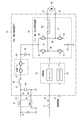
- FIG. 2 is a circuit configuration diagram of the ECU of each embodiment.
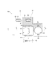
- FIG. 3 is a plan view of the ECU board of the first embodiment.
- FIG. 4 is a schematic diagram illustrating a substrate mounting configuration of the filter circuit unit of the ECU according to the first embodiment.
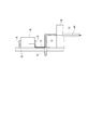
- FIG. 5 is a side view showing the connection between the power supply voltage terminal and the surface mount inductor.
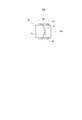
- FIG. 6A is a plan view of a surface mount inductor
- 6B is a view in the direction of the arrow VIB in FIG.
- FIG. 6C is a view in the direction of the VIC arrow in FIG.
- FIG. 7 is a schematic diagram illustrating a substrate mounting configuration of the filter circuit unit of the ECU according to the second embodiment.
- FIG. 8 is a schematic diagram illustrating a substrate mounting configuration of the filter circuit unit of the ECU according to the third embodiment.
- FIG. 9 is a schematic diagram illustrating a substrate mounting configuration of the filter circuit unit of the ECU according to the fourth embodiment.
- the electric power steering device 90 includes a motor 80 as a “load” that outputs a steering assist torque, and an ECU 10 as a “power conversion device” that supplies electric power to the motor 80.
- the ECU 10 converts the DC power of the battery 15 as “DC power supply” based on the torque signal trq from the torque sensor 95 provided on the steering shaft 92 and supplies the converted DC power to the motor 80.
- the motor 80 rotates forward when the handle 91 is rotated to the right, for example, and reversely rotated when the handle 91 is rotated to the left, according to the steering direction of the driver.
- the electric power steering device 90 illustrated in FIG. 1 is of a rack assist type in which a motor 80 is attached to a rack shaft 93, but this embodiment is similarly applied to a column assist type electric power steering device. Is possible.
- the ECU 10 includes a power unit 60 including a power conversion circuit, and a control unit 70 that controls energization of the power unit 60.
- the power unit 60 includes an H bridge circuit in which four switching elements 61-64 are bridge-connected as a power conversion circuit.
- the switching elements 61-64 for example, MOSFETs (that is, metal oxide semiconductor field effect transistors) are used.
- the first node N1 that is an intermediate point of one half bridge of the H bridge circuit and the second node N2 that is an intermediate point of the other half bridge are connected to motor terminals 37 and 38, respectively.
- a motor relay 65 that prevents input of induced power from the motor 80 is provided in the power path LP that connects the first node N1 and the second node N2 via the motor 80.
- a shunt resistor 67 for current detection is provided on the ground side of the H bridge circuit.
- the control unit 70 acquires vehicle information such as a torque signal trq and a vehicle speed signal. In addition, current information detected by the power unit 60 is fed back, and a switching signal is output to the power conversion circuit of the power unit 60 based on the information.
- the control unit 70 controls the energization and rotation direction of the motor 80.
- a microcomputer 41, a custom IC 42, and the like are used as board mounting components constituting the control unit 70.
- the driving power supplied to the power unit 60 and the control power for operation of the control unit 70 are supplied from the common battery 15.
- the power supply voltage terminal 33 of the ECU 10 is connected to the positive electrode of the battery 15 via the PIG line of the power supply harness 16.
- the ground terminal 34 is grounded via the PGND line of the power harness 16.
- the IG line to which the control power is input is turned on / off by the ignition switch 17.
- a power supply relay 45 capable of interrupting the conduction of the PIG line.
- the power supply relay 45 is configured with two MOSFETs connected in series with the directions of the parasitic diodes opposite to each other in consideration of protection when the polarity of the battery 15 is erroneously reversely connected.
- the power relay 45 may be configured by an electromagnetic open / close mechanical relay.
- a filter circuit including an inductor 40 and a capacitor 50 is provided in front of the power supply relay 45.
- the inductor 40 has an input end 43 connected to the power supply voltage terminal 33 and an output end 44 connected to the power supply relay 45 on the PIG line.
- the capacitor 50 has one electrode terminal 53 connected to the input end 43 of the inductor 40 and the other electrode terminal 54 connected to the ground terminal 34.
- the filter circuit removes disturbance noise that enters the ECU 10 from the external power supply harness 16, and also removes switching noise that is generated in association with the switching operation of the power unit 60 and goes out from the ECU 10.
- “Noise resistance performance” to be described later means a removal capability for both of these noises.
- a post-relay capacitor 55 that smoothes the input power to the power unit 60 is provided.
- the term “capacitor 50 before relay” corresponds to the “capacitor 55 after relay” and the capacitor 50 connected to the input terminal 43 of the inductor 40 is “capacitor 50 before relay”.
- the “pre-relay capacitor 50” is omitted, and is simply referred to as “capacitor 50”.
- the capacitor 50 in front of the power relay 45 corresponds to a “capacitor”.
- a surface mount type inductor is used as the inductor 40 instead of the choke coil type.
- a plurality of capacitor elements may be connected in parallel in the actual board mounting for the capacitor 50 and the post-relay capacitor 55 each illustrated by one electrical symbol. That is, the electrical symbol of one capacitor in FIG. 2 is interpreted as meaning “one or more capacitors” as a substance.
- Patent Document 1 Japanese Patent Laid-Open No. 2015-126097
- a surface mount inductor and a plurality of inductors are provided after the power relay. It is presumed that a post-relay capacitor is provided.
- a general idea is that a power relay is provided immediately after the power supply voltage terminal so that a voltage is not applied to the inductor or the capacitor when the relay is cut off.
- the inductor 40 and the capacitor 50 are disposed in front of the power relay 45 in order to improve the heat dissipation of the inductor in comparison with such a conventional layout.
- the configuration of the present embodiment in which the surface-mount type inductor 40 and the capacitor 50 are arranged in front of the power supply relay 45 clarifies the contribution to the prior art.
- the element arrangement in order to improve the heat dissipation of the inductor 40, the element arrangement is devised more specifically with respect to the substrate mounting configuration of the filter circuit unit of the ECU 10.
- the board mounting configuration of the present embodiment aimed at improving the heat dissipation of the inductor 40, which is not focused on in the prior art, is not a so-called design item.
- details of the substrate mounting configuration will be described for each embodiment.
- the number of the embodiment is attached to the third digit following “10”.
- FIG. 3 is a plan view of the substrate 20 on which the circuit of the ECU 101 is mounted, and corresponds to FIG.
- the following description of the mounting configuration will be basically based on the plan view which is the viewing direction of FIG.
- the substrate 20 is made of an insulating material such as glass epoxy or ceramic.
- a wiring pattern such as a power supply pattern 21 is formed of a conductive material such as copper. In FIG. 3, illustration of wiring patterns other than the power supply pattern 21 is omitted.
- illustration of the arrangement of the post-relay capacitor 55, the arrangement of the switching elements 61-64 in the power unit 60, and the arrangement of the microcomputer 71 and the custom IC 72 in the control unit 70 is omitted. Further, illustration and explanation of a heat sink, a heat radiating gel, and the like that mainly contribute to heat radiation of the switching elements 61-64, which are described in detail in Patent Document 1, are omitted.
- the connector section 30 includes a power supply voltage terminal 33, a ground terminal 34, motor terminals 37 and 38, and a control terminal 39 corresponding to the circuit diagram of FIG.
- the control terminal 39, the terminal into which the control electric power from an IG line is input, and the terminal into which a vehicle information signal is input are included by one code
- the harness including at least the PIG line is the power harness 16.
- the power supply voltage terminal 33, the ground terminal 34, and the motor terminals 37 and 38 are respectively inserted into terminal holes 23, 24, 27, and 28 formed in the substrate 20 and electrically connected to corresponding wiring patterns by soldering or the like. Is done. Of the connection configurations of these terminals, the motor terminals 37 and 38 are not further described.
- the power supply voltage terminal 33 and the ground terminal 34 have a rectangular cross section so as to be advantageous for energizing a large current.
- the first terminal hole 23 into which the power supply voltage terminal 33 is inserted and the second terminal hole 24 into which the ground terminal 34 is inserted are formed in an elongated hole shape.
- FIG. 4 the region of the power supply pattern 21 formed on the surface layer of the substrate 20 is illustrated with a satin finish. Further, a portion of the ground pattern 22 formed on the surface layer of the substrate 20 that connects the electrode terminal 54 of the capacitor 50 and the ground terminal 34 is indicated by a broken line frame.
- the ground pattern 22 is connected in common to the ground-side contacts of the post-relay capacitor 55, the power unit 60, and the control unit 70.
- the entire surface layer area other than the power supply pattern 21 and other wiring pattern areas may be used as the ground pattern 22.
- the connection between the electrode terminal 54 of the capacitor 50 and the ground terminal 34 is particularly displayed, and therefore the illustration of the ground pattern 22 in other parts is omitted.
- the power supply pattern 21 has a long first terminal hole 23 into which a power supply voltage terminal 33 having a rectangular cross section is inserted.
- a long second terminal hole 24 into which a ground terminal 34 having a rectangular cross section is inserted is formed in the ground pattern 22.
- the first terminal hole 23 and the second terminal hole 24 have a long hole shape obtained by translating a circular hole in one direction.
- the first terminal hole 23 and the second terminal hole 24 are not limited to this shape.
- a rectangular shape with rounded corners can be inserted without interference between the power supply voltage terminal 33 and the ground terminal 34. Any shape may be used.
- the power supply voltage terminal 33 and the ground terminal 34 inserted into the first terminal hole 23 and the second terminal hole 24 are electrically connected to the power supply pattern 21 and the ground pattern 22 by soldering or the like.
- the longitudinal axis direction of the first terminal hole 23 is defined as “x direction”.
- the longitudinal axis of the first terminal hole 23 and the longitudinal axis of the second terminal hole 24 are arranged on the same straight line.
- the second terminal holes 24 may be offset in parallel to the first terminal holes 23 or may be arranged non-parallel.
- the total length of the first terminal hole 23 in the x direction is represented as Wh.
- the power supply pattern 21 is connected to the input terminal 43 of the inductor 40 and one electrode terminal 53 of the capacitor 50.
- the other electrode terminal 54 of the capacitor 50 is connected to the ground pattern 22.
- a surface mount type inductor 40 is used as an inductor constituting the filter circuit.
- FIG. 6A, 6B, and 6C are three views of a surface-mount inductor 40 that has a substantially rectangular parallelepiped shape.
- the illustration of the coil 41 in the plan view of FIG. 6A is a schematic representation of an electrical symbol and does not represent the shape of the substance.
- the coil 41 is wound around the core of the main body 42.
- the input end 43 and the output end 44 of the coil 41 are opposed to a rectangular parallelepiped. Therefore, the wall surfaces of the input end 43 and the output end 44 are orthogonal to the connection direction of the coil 41 that connects the input end 43 and the output end 44 with the shortest distance.
- the input end 43 and the output end 44 may be formed interchangeably without distinction.
- an end connected to the power supply pattern 21 is referred to as an input end 43
- an end connected to the wiring pattern on the power supply relay 45 side is referred to as an output end 44.
- the wiring pattern on the power relay 45 side is not shown.
- the width of the input end 43 is represented as Wt. In FIG. 4, the width Wp of the power supply pattern 21 in the portion connecting the first terminal hole 23 and the input end 43 is formed larger than the width Wt of the input end 43.
- the capacitor 50 may be an electrolytic capacitor having polarity or a nonpolar capacitor.
- the electrode terminal connected to the power supply pattern 21 is the first electrode terminal 53 and the electrode terminal connected to the ground pattern 22 is the second electrode terminal regardless of the presence or absence of polarity. 54.
- ECU101 of 1st Embodiment has the following points regarding the board
- the wall surface of the input end 43 is arranged in parallel with the x direction which is the longitudinal axis direction of the first terminal hole 23. Therefore, the connection direction of the coil 41 orthogonal to the wall surface of the input end 43 is defined as the “y direction” orthogonal to the x direction.
- the xy coordinate axes are described as a reference. In the x direction, at least part of the width Wt of the input end 43 and the total length Wh of the first terminal hole 23 overlap.
- the heat generation Q of the inductor 40 is transmitted from the input end 43 to the power supply voltage terminal 33 inserted into the first terminal hole 23 via the power supply pattern 21 on the surface layer of the substrate 20, and further to the connector.
- the power is transmitted from the unit 30 to the power harness 16. Therefore, in the heat transfer path of the power supply pattern 21 that connects the input end 43 and the first terminal hole 23, the input end 43 and the first terminal hole 23 are arranged so that at least a part thereof is opposed to the heat transfer path.
- the path can be effectively secured and the heat dissipation of the inductor 40 can be improved.
- the distance D1 between the input end 43 and the first terminal hole 23 is preferably set to be as short as possible in production.
- the steering assist motor 80 of the electric power steering device 90 is required to generate a large output suddenly, a large current flows through the inductor 40 and the power unit 60 of the PIG line and generates heat. Moreover, the space for mounting the vehicle is restricted, and the ECU 101 must be made small, so that natural cooling is relatively disadvantageous. Therefore, with the above configuration, the effect of improving the heat dissipation of the inductor 40 is particularly effectively exhibited.
- the inductor 40 faces the first terminal hole 23 in the x direction so as to include the entire length Wh of the first terminal hole 23 within the range of the width Wt of the input end 43. . Thereby, the heat transfer path of the power supply pattern 21 on the surface layer of the substrate 20 can be particularly effectively ensured.
- the direction connecting the first electrode terminal 53 and the second electrode terminal 54 is the y direction parallel to the connection direction of the inductor 40, and the second electrode terminal 54 is close to the second terminal hole 24. Arranged on the side.
- “parallel to the connection direction” is not limited to strict parallel, but includes a range that can be interpreted as being substantially parallel.
- the direction connecting the first electrode terminal 53 and the second electrode terminal 54 does not coincide with the x direction, and either the first electrode terminal 53 or the second electrode terminal 54 is closer to the second terminal hole 24. All forms that can be determined may be interpreted as “connection direction, that is, parallel to the y direction”. Thereby, the distance between the second electrode terminal 54 and the ground terminal 34 is made as short as possible, and the loop area of the filter circuit is reduced, so that the noise resistance can be improved.
- the center position C C of the capacitor 50 is offset toward the second terminal hole 24 side with respect to the center position C L of the inductor 40 in the y direction. This is advantageous for shortening the distance between the second electrode terminal 54 and the ground terminal 34, and can further improve noise resistance.
- FIGS. 7 and 8 corresponding to FIG. 4 of the first embodiment. This will be described with reference to FIG. In the following description of the embodiment, the same reference numerals are given to substantially the same components as those in the first embodiment, and the description thereof is omitted.
- the ECU 102 of the second embodiment shown in FIG. 7 differs from the first embodiment in that two capacitors 501 and 502 are connected in parallel before the power relay 45.
- the center positions C C1 and C C2 of the two capacitors 501 and 502 are both located on the second terminal hole 24 side with respect to the center position C L of the inductor 40.
- the second electrode terminals 54 of the capacitors 501 and 502 are both arranged on the side close to the second terminal hole 24 in the y direction.
- the filter circuit of the input unit may be configured by three or more pre-relay capacitors connected in parallel between the power supply pattern 21 and the ground pattern 22.
- the center position of at least one of the capacitors is located on the second terminal hole 24 side with respect to the center position C L of the inductor 40.
- the ECU 103 of the third embodiment shown in FIG. 8 differs from the first embodiment in the positional relationship between the inductor 40 and the first terminal hole 23.
- the range Wt of the input end 43 of the inductor 40 does not completely include the range Wh of the first terminal hole 23, and a part thereof overlaps.
- the distance D1 between the input end 43 and the first terminal hole 23 is preferably set to be as short as possible, as in the first embodiment.
- the third embodiment has the same effects as the effects (1), (3), and (4) of the first embodiment.
- the ECU 104 of the fourth embodiment shown in FIG. 9 differs from the first embodiment in the positional relationship between the inductor 40 and the capacitor 50.
- the center position C C of the capacitor 50 is substantially the same as the center position C L of the inductor 40.
- the capacitor 50 is disposed directly beside the inductor 40.
- the fourth embodiment has the same effects as the effects (1) and (2) of the first embodiment.
- (C) It is good also as a power converter device which equips the above-mentioned embodiment which drives a DC motor with a three-phase inverter as a power converter circuit of a power part, and drives a three-phase AC motor as a load.
- the power conversion device of the present disclosure is not limited to a device that drives a steering assist motor of an electric power steering device, but can be applied to any power conversion device that converts power input from a DC power source and outputs it to some load. is there.
Landscapes
- Engineering & Computer Science (AREA)
- Power Engineering (AREA)
- Microelectronics & Electronic Packaging (AREA)
- Chemical & Material Sciences (AREA)
- Mechanical Engineering (AREA)
- Transportation (AREA)
- Combustion & Propulsion (AREA)
- General Physics & Mathematics (AREA)
- Automation & Control Theory (AREA)
- Radar, Positioning & Navigation (AREA)
- Electromagnetism (AREA)
- Physics & Mathematics (AREA)
- Inverter Devices (AREA)
- Structure Of Printed Boards (AREA)
- Power Steering Mechanism (AREA)
- Control Of Electrical Variables (AREA)
Abstract
断面が長方形状である電源電圧端子(33)及びグランド端子(34)は、それぞれ、電源パターン(21)の第1端子穴(23)、及び、グランドパターン(22)の第2端子穴(24)に挿入されている。インダクタ(40)は、基板(20)に表面実装され、電源パターン(21)に接続される入力端(43)と、電源リレー(45)に接続される出力端(44)とが対面をなす直方体を呈する。コンデンサ(50)は、第1電極端子(53)が電源パターン(21)に接続され、第2電極端子(54)がグランドパターン(22)に接続され、インダクタ(40)と共にフィルタ回路を構成する。インダクタ(40)は、入力端(43)の壁面が第1端子穴(23)の長手軸方向(x方向)と平行に配置されている。且つ、インダクタ(40)は、x方向において、入力端(23)の幅Wtの範囲内に第1端子穴(23)の全長Whを含むように第1端子穴(23)と対向している。
Description
本出願は、2016年6月1日に出願された特許出願番号2016-109834号に基づくものであり、ここにその記載内容を援用する。
本開示は、直流電源から入力される電力を変換し負荷に出力する電力変換装置、及び、これを用いた電動パワーステアリング装置に関する。
従来、バッテリ等の直流電源から入力される電力を変換し、モータ等の負荷に出力する電力変換装置が知られている。例えば電動パワーステアリング装置の操舵アシストモータを駆動する電力変換装置では、搭載スペースの制約により、大電流が通電されるパワー部と、マイコン等を含む制御部とが同一の基板上に並べて配置される。そのため、基板上の素子の発熱を好適に放熱させることが特に重要である。
例えば特許文献1に開示された装置は、基板に実装されたスイッチング素子の発熱を、ランドパターンを経由してコネクタ側へ放熱させるとともに、放熱ゲルを介してヒートシンクに放熱させる。
例えば特許文献1に開示された装置は、基板に実装されたスイッチング素子の発熱を、ランドパターンを経由してコネクタ側へ放熱させるとともに、放熱ゲルを介してヒートシンクに放熱させる。
一般に電力変換装置の入力部には、電源ハーネスから装置に入ってくる外乱ノイズや、装置から外部へ出て行くスイッチングノイズを除去するため、インダクタ及びコンデンサを含むフィルタ回路が設けられる。また、フィルタ回路のインダクタとしては、円筒状のコアに巻線を巻回した従来のチョークコイルに代えて、近年、小型化に有利な表面実装型インダクタが用いられる傾向がある。
特許文献1の装置は、スイッチング素子の放熱性向上を図っているものの、表面実装型インダクタの放熱に関しては考慮していない。したがって、基板に搭載された素子全体の放熱性としては不十分である。
本開示の目的は、表面実装型インダクタの放熱性を向上させる電力変換装置を提供することにある。
特許文献1の装置は、スイッチング素子の放熱性向上を図っているものの、表面実装型インダクタの放熱に関しては考慮していない。したがって、基板に搭載された素子全体の放熱性としては不十分である。
本開示の目的は、表面実装型インダクタの放熱性を向上させる電力変換装置を提供することにある。
本開示は、直流電源から電源ハーネスを経由して入力される電力を電力変換回路の動作により変換し、負荷に出力する電力変換装置である。この電力変換装置は、基板と、コネクタ部と、電源パターンと、グランドパターンと、電源リレーと、インダクタと、一つ以上のコンデンサとを備える。
コネクタ部は、断面が長方形状である電源電圧端子及びグランド端子を有し、電源ハーネスを挿着可能である。
電源パターンは、基板の表層に形成され、電源電圧端子が挿入される長形の第1端子穴を有する。
グランドパターンは、基板の表層に形成され、グランド端子が挿入される長形の第2端子穴を有する。
電源リレーは、電力変換回路の入力部に設けられ、電力経路を遮断可能である。
電源パターンは、基板の表層に形成され、電源電圧端子が挿入される長形の第1端子穴を有する。
グランドパターンは、基板の表層に形成され、グランド端子が挿入される長形の第2端子穴を有する。
電源リレーは、電力変換回路の入力部に設けられ、電力経路を遮断可能である。
インダクタは、基板に表面実装され、電源パターンに接続される入力端と、電源リレーに接続される出力端とが対面をなす直方体を呈する。ここで「直方体」とは厳密な直方体に限らず、全体がほぼブロック状である「略直方体」を意味する。
一つ以上のコンデンサは、一方の電極端子が電源パターンに接続され、他方の電極端子がグランドパターンに接続され、インダクタと共にフィルタ回路を構成する。
一つ以上のコンデンサは、一方の電極端子が電源パターンに接続され、他方の電極端子がグランドパターンに接続され、インダクタと共にフィルタ回路を構成する。
インダクタは、入力端の壁面が第1端子穴の長手軸方向と平行に配置されており、且つ、第1端子穴の長手軸方向において、入力端の幅と第1端子穴の全長とは、少なくとも一部が重複している。好ましくは、インダクタは、第1端子穴の長手軸方向において、入力端の幅の範囲内に第1端子穴の全長を含むように第1端子穴と対向している。また、製造上可能な限り、第1端子穴からインダクタの入力端までの距離は、可及的に短く設定されることが好ましい。
これにより、表面実装型インダクタから電源電圧端子を経由して電源ハーネスへ好適に放熱させることができる。
これにより、表面実装型インダクタから電源電圧端子を経由して電源ハーネスへ好適に放熱させることができる。
さらに、コンデンサは、基板に表面実装され、二つの電極端子を結ぶ方向がインダクタの入力端と出力端とを結ぶ結線方向と平行であり、グランドパターンに接続される電極端子が第2端子穴に近い側に配置されていることが好ましい。コンデンサとグランド端子との距離を可及的に短くし、フィルタ回路のループ面積を小さくすることで、耐ノイズ性能を向上させることができる。
本開示の電力変換装置は、例えば、車両の電動パワーステアリング装置において、操舵アシストモータを駆動する装置として適用される。電動パワーステアリング装置の操舵アシストモータは、大きな出力を急に発生させることが要求されるため、インダクタや電力変換回路に大電流が流れ、発熱する。しかも、車両の搭載スペースが制約され、電力変換装置を小型にせざるを得ないため、自然冷却が比較的不利になる。したがって、本開示の構成により、インダクタの放熱性を向上させる効果が特に有効に発揮される。
本開示についての上記目的及びその他の目的、特徴や利点は、添付の図面を参照しながら下記の詳細な記述により、より明確になる。その図面は、
図1は、各実施形態のECU(電力変換装置)が適用される電動パワーステアリング装置の全体模式図であり、
図2は、各実施形態のECUの回路構成図であり、
図3は、第1実施形態のECU基板の平面図であり、
図4は、第1実施形態のECUのフィルタ回路部の基板実装構成を示す模式図であり、
図5は、電源電圧端子と表面実装型インダクタとの接続を示す側面図であり、
図6Aは、表面実装型インダクタの平面図であり、、
図6Bは、図6AのVIB方向矢視図であり、
図6Cは、図6AのVIC方向矢視図であり、
図7は、第2実施形態のECUのフィルタ回路部の基板実装構成を示す模式図であり、
図8は、第3実施形態のECUのフィルタ回路部の基板実装構成を示す模式図であり、
図9は、第4実施形態のECUのフィルタ回路部の基板実装構成を示す模式図である。
以下、電力変換装置の複数の実施形態を図面に基づいて説明する。これらの実施形態の電力変換装置は、例えば車両の電動パワーステアリング装置において、操舵アシストトルクを出力するモータに電力を供給する装置として適用される。以下の第1~第4実施形態を包括して、「本実施形態」という。
最初に図1を参照し、電動パワーステアリング装置の概略構成について説明する。
電動パワーステアリング装置90は、操舵アシストトルクを出力する「負荷」としてのモータ80、及び、モータ80に電力を供給する「電力変換装置」としてのECU10を備える。
最初に図1を参照し、電動パワーステアリング装置の概略構成について説明する。
電動パワーステアリング装置90は、操舵アシストトルクを出力する「負荷」としてのモータ80、及び、モータ80に電力を供給する「電力変換装置」としてのECU10を備える。
ECU10は、ステアリングシャフト92に設けられたトルクセンサ95からのトルク信号trqに基づき、「直流電源」としてのバッテリ15の直流電力を変換してモータ80に供給する。モータ80は、運転者の操舵方向に応じて、例えばハンドル91を右に回すとき正転し、ハンドル91を左に回すとき逆転する。
なお、図1に例示する電動パワーステアリング装置90は、モータ80がラック軸93に取り付けられるラックアシスト式のものであるが、本実施形態は、コラムアシスト式の電動パワーステアリング装置にも同様に適用可能である。
なお、図1に例示する電動パワーステアリング装置90は、モータ80がラック軸93に取り付けられるラックアシスト式のものであるが、本実施形態は、コラムアシスト式の電動パワーステアリング装置にも同様に適用可能である。
次に図2を参照し、操舵アシストモータ80がDCモータである場合を例として、ECU10の回路構成について説明する。ECU10は、電力変換回路を含むパワー部60、及び、パワー部60の通電を制御する制御部70を有する。
駆動対象がDCモータ80の場合、パワー部60は、電力変換回路として、四つのスイッチング素子61-64がブリッジ接続されたHブリッジ回路を含む。スイッチング素子61-64としては、例えばMOSFET(すなわち、金属酸化物半導体電界効果トランジスタ)が用いられる。
駆動対象がDCモータ80の場合、パワー部60は、電力変換回路として、四つのスイッチング素子61-64がブリッジ接続されたHブリッジ回路を含む。スイッチング素子61-64としては、例えばMOSFET(すなわち、金属酸化物半導体電界効果トランジスタ)が用いられる。
Hブリッジ回路の一方のハーフブリッジの中間点である第1ノードN1、及び、他方のハーフブリッジの中間点である第2ノードN2は、それぞれモータ端子37、38に接続される。第1ノードN1と第2ノードN2との間を、モータ80を経由して結ぶ電力経路LPには、モータ80からの誘起電力の入力を防止するモータリレー65が設けられる。また、例えばHブリッジ回路のグランド側には、電流検出用のシャント抵抗67が設けられる。
制御部70は、トルク信号trqや車速信号等の車両情報を取得する。また、パワー部60で検出された電流情報等がフィードバックされ、これらの情報に基づいて、パワー部60の電力変換回路にスイッチング信号を出力する。駆動対象がDCモータ80の場合、制御部70は、モータ80の通電及び回転方向を制御する。
なお、制御部70を構成する基板実装部品として、マイコン41及びカスタムIC42等が用いられる。
なお、制御部70を構成する基板実装部品として、マイコン41及びカスタムIC42等が用いられる。
パワー部60に通電される駆動用電力、及び、制御部70の動作用の制御電力は、共通のバッテリ15から供給される。
ECU10の電源電圧端子33は、電源ハーネス16のPIGラインを経由してバッテリ15の正極に接続される。グランド端子34は、電源ハーネス16のPGNDラインを経由して接地される。また、制御電力が入力されるIGラインは、イグニションスイッチ17により導通がオン/オフされる。
ECU10の電源電圧端子33は、電源ハーネス16のPIGラインを経由してバッテリ15の正極に接続される。グランド端子34は、電源ハーネス16のPGNDラインを経由して接地される。また、制御電力が入力されるIGラインは、イグニションスイッチ17により導通がオン/オフされる。
電源電圧端子33とパワー部60との間には、PIGラインの導通を遮断可能な電源リレー45が設けられる。電源リレー45は、バッテリ15の極性を誤って逆接続した場合の保護も考慮し、例えば、寄生ダイオードの向きが互いに反対向きに直列接続された二つのMOSFETにより構成される。或いは、電磁開閉式のメカリレーで電源リレー45を構成してもよい。
以下、電源リレー45の「前」とは、入力側、すなわち電源電圧端子33側を意味し、電源リレー45の「後ろ」とはパワー部60側を意味する。
本実施形態では、電源リレー45の前に、インダクタ40及びコンデンサ50からなるフィルタ回路が設けられる。インダクタ40は、PIGライン上において入力端43が電源電圧端子33に接続され、出力端44が電源リレー45に接続される。コンデンサ50は、一方の電極端子53がインダクタ40の入力端43に接続され、他方の電極端子54がグランド端子34に接続される。
本実施形態では、電源リレー45の前に、インダクタ40及びコンデンサ50からなるフィルタ回路が設けられる。インダクタ40は、PIGライン上において入力端43が電源電圧端子33に接続され、出力端44が電源リレー45に接続される。コンデンサ50は、一方の電極端子53がインダクタ40の入力端43に接続され、他方の電極端子54がグランド端子34に接続される。
フィルタ回路は、外部の電源ハーネス16からECU10に入ってくる外乱ノイズを除去すると共に、パワー部60のスイッチング動作に伴って発生し、ECU10から外部に出ていくスイッチングノイズを除去する。後述する「耐ノイズ性能」とは、これらの両方のノイズに対する除去能力を意味する。
電源リレー45の後ろには、パワー部60への入力電力を平滑化するリレー後コンデンサ55が設けられる。厳格に用語を使い分けると、「リレー後コンデンサ55」に対応して、インダクタ40の入力端43に接続されるコンデンサ50は、「リレー前コンデンサ50」となる。ただし、以下の説明では、リレー後コンデンサ55にほとんど着目せず、専らリレー前のコンデンサ50に言及する。そのため、「リレー前コンデンサ50」を省略し、単に「コンデンサ50」と記す。電源リレー45前のコンデンサ50は、「コンデンサ」に相当する。
後述のように本実施形態の基板実装構成では、インダクタ40として、チョークコイル型のものでなく、表面実装型のインダクタが用いられる。
また、図2において、それぞれ一つの電気記号で図示されるコンデンサ50及びリレー後コンデンサ55について、現実の基板実装では、複数のコンデンサ素子が並列に接続されてもよい。すなわち、図2における一つのコンデンサの電気記号は、実体として「一つ以上のコンデンサ」を意味するものとして解釈される。
また、図2において、それぞれ一つの電気記号で図示されるコンデンサ50及びリレー後コンデンサ55について、現実の基板実装では、複数のコンデンサ素子が並列に接続されてもよい。すなわち、図2における一つのコンデンサの電気記号は、実体として「一つ以上のコンデンサ」を意味するものとして解釈される。
ところで、特許文献1(特開2015-126097号公報)に開示された従来技術では、インダクタの放熱に関して考慮されていない。
特許文献1の明細書には明示されていないものの、特許文献1の図3、図4等の記載から当業者の技術常識に基づいて判断すると、電源リレーの後に、表面実装型のインダクタ及び複数のリレー後コンデンサが設けられていると推測される。また、従来の技術常識によると、電源電圧端子の直後に電源リレーを設け、リレー遮断時に、インダクタやコンデンサに電圧が印加されることを回避する考え方が一般的である。
特許文献1の明細書には明示されていないものの、特許文献1の図3、図4等の記載から当業者の技術常識に基づいて判断すると、電源リレーの後に、表面実装型のインダクタ及び複数のリレー後コンデンサが設けられていると推測される。また、従来の技術常識によると、電源電圧端子の直後に電源リレーを設け、リレー遮断時に、インダクタやコンデンサに電圧が印加されることを回避する考え方が一般的である。
本実施形態では、このような従来技術のレイアウトに対し、インダクタの放熱性向上のため、電源リレー45の前にインダクタ40及びコンデンサ50を配置する。要するに、電源リレー45の前に表面実装型のインダクタ40及びコンデンサ50を配置するという本実施形態の構成は、それ自体、従来技術に対する貢献を明示するものである。
それに加え本実施形態では、インダクタ40の放熱性を向上させるため、ECU10のフィルタ回路部の基板実装構成に関し、より具体的に素子配置を工夫する。このように、従来技術では全く着目していないインダクタ40の放熱性向上を目的とする本実施形態の基板実装構成は、いわゆる設計事項に該当するものではない。
以下、基板実装構成の詳細について実施形態毎に説明する。各実施形態のECU10の符号として、「10」に続く3桁目に実施形態の番号を付す。
以下、基板実装構成の詳細について実施形態毎に説明する。各実施形態のECU10の符号として、「10」に続く3桁目に実施形態の番号を付す。
(第1実施形態)
第1実施形態について、図3~図6を参照して説明する。図3は、ECU101の回路が実装された基板20の平面図であり、特許文献1の図3等に対応するものである。以下の実装構成の説明は、基本的に図3の視方向である平面視を基準として記述する。
基板20は、ガラスエポキシやセラミック等の絶縁性材料で形成されている。基板20の表層には、電源パターン21等の配線パターンが銅等の導電性物質で形成されている。図3には、電源パターン21以外の配線パターンの図示を省略する。
第1実施形態について、図3~図6を参照して説明する。図3は、ECU101の回路が実装された基板20の平面図であり、特許文献1の図3等に対応するものである。以下の実装構成の説明は、基本的に図3の視方向である平面視を基準として記述する。
基板20は、ガラスエポキシやセラミック等の絶縁性材料で形成されている。基板20の表層には、電源パターン21等の配線パターンが銅等の導電性物質で形成されている。図3には、電源パターン21以外の配線パターンの図示を省略する。
本実施形態では、リレー後コンデンサ55の配置、パワー部60におけるスイッチング素子61-64の配置、並びに、制御部70におけるマイコン71及びカスタムIC72の配置については、図示を省略する。
また、特許文献1に詳しく記載されている、主にスイッチング素子61-64の放熱に寄与するヒートシンクや放熱ゲル等に関する図示及び説明を省略する。
また、特許文献1に詳しく記載されている、主にスイッチング素子61-64の放熱に寄与するヒートシンクや放熱ゲル等に関する図示及び説明を省略する。
略長方形の基板20の一辺には、電力や信号を外部と入出力するためのハーネスを挿着可能なコネクタ部30が設けられる。コネクタ部30には、図2の回路図に対応する電源電圧端子33、グランド端子34、モータ端子37、38及び制御端子39が含まれる。制御端子39については、IGラインからの制御電力が入力される端子と、車両情報信号が入力される端子とを一つの符号で包括する。また、各端子に対応する複数のハーネスをどのようにグループ分けするかは適宜設定してよい。少なくともPIGラインが含まれるハーネスが電源ハーネス16である。
電源電圧端子33、グランド端子34及びモータ端子37、38は、それぞれ基板20に形成された端子穴23、24、27、28に挿入され、はんだ付け等により対応する各配線パターンに電気的に接続される。これらの端子の接続構成のうち、モータ端子37、38については、それ以上の言及をしない。
電源電圧端子33及びグランド端子34は、大電流の通電に有利なように、断面が長方形状に形成されている。それに対応し、電源電圧端子33が挿入される第1端子穴23、及び、グランド端子34が挿入される第2端子穴24は、長穴状に形成されている。
電源電圧端子33及びグランド端子34は、大電流の通電に有利なように、断面が長方形状に形成されている。それに対応し、電源電圧端子33が挿入される第1端子穴23、及び、グランド端子34が挿入される第2端子穴24は、長穴状に形成されている。
続いて図4、図6A、6B、6Cを参照し、第1実施形態のECU101のフィルタ回路部の基板実装構成について説明する。
図4にて、基板20の表層に形成された電源パターン21の領域を梨地で図示する。
また、基板20の表層に形成されたグランドパターン22のうち、コンデンサ50の電極端子54とグランド端子34とを接続する部分を破線枠で示す。
図4にて、基板20の表層に形成された電源パターン21の領域を梨地で図示する。
また、基板20の表層に形成されたグランドパターン22のうち、コンデンサ50の電極端子54とグランド端子34とを接続する部分を破線枠で示す。
図2に参照されるように、グランドパターン22は、リレー後コンデンサ55、パワー部60、制御部70のグランド側接点に共通に接続される。例えば現実の製品では、電源パターン21や他の配線パターンの領域以外の表層領域全体をグランドパターン22としてもよい。ただし、図4等では、コンデンサ50の電極端子54とグランド端子34との接続を特に表示するため、その他の部分のグランドパターン22の図示を省略する。
電源パターン21には、断面が長方形状の電源電圧端子33が挿入される長形の第1端子穴23が形成されている。同様にグランドパターン22には、断面が長方形状のグランド端子34が挿入される長形の第2端子穴24が形成されている。
図4の例では、第1端子穴23及び第2端子穴24は、円形穴を一方向に平行移動させて得られる長穴形状を呈している。ただし、第1端子穴23及び第2端子穴24は、この形状に限らず、例えば角丸めされた長方形等のように、電源電圧端子33及びグランド端子34が干渉することなく挿入可能な「長形」の形状であればよい。
図4の例では、第1端子穴23及び第2端子穴24は、円形穴を一方向に平行移動させて得られる長穴形状を呈している。ただし、第1端子穴23及び第2端子穴24は、この形状に限らず、例えば角丸めされた長方形等のように、電源電圧端子33及びグランド端子34が干渉することなく挿入可能な「長形」の形状であればよい。
第1端子穴23及び第2端子穴24に挿入された電源電圧端子33及びグランド端子34は、はんだ付け等により、電源パターン21及びグランドパターン22と電気的に接続される。
以下、第1端子穴23の長手軸方向を「x方向」と定義する。図4の例では、第1端子穴23の長手軸と第2端子穴24の長手軸とは同一直線上に配置されている。なお、他の実施形態では、第2端子穴24は、第1端子穴23に対し平行にオフセットしてもよく、非平行に配置されてもよい。ここで、第1端子穴23のx方向の全長をWhと表す。
以下、第1端子穴23の長手軸方向を「x方向」と定義する。図4の例では、第1端子穴23の長手軸と第2端子穴24の長手軸とは同一直線上に配置されている。なお、他の実施形態では、第2端子穴24は、第1端子穴23に対し平行にオフセットしてもよく、非平行に配置されてもよい。ここで、第1端子穴23のx方向の全長をWhと表す。
電源パターン21には、インダクタ40の入力端43、及び、コンデンサ50の一方の電極端子53が接続される。グランドパターン22には、コンデンサ50の他方の電極端子54が接続される。
本実施形態では、フィルタ回路を構成するインダクタとして、表面実装型のインダクタ40が用いられる。
本実施形態では、フィルタ回路を構成するインダクタとして、表面実装型のインダクタ40が用いられる。
図6A、6B、6Cに、略直方体を呈する表面実装型インダクタ40の三面図を示す。図6Aの平面図におけるコイル41の図示は電気記号を模式的に示したものであり、実体の形状を表すものではない。コイル41は、本体42のコアに巻回されている。
コイル41の入力端43と出力端44とは、直方体の対面をなしている。したがって、入力端43及び出力端44の壁面は、入力端43と出力端44とを最短距離で結ぶコイル41の結線方向に対して直交する。
コイル41の入力端43と出力端44とは、直方体の対面をなしている。したがって、入力端43及び出力端44の壁面は、入力端43と出力端44とを最短距離で結ぶコイル41の結線方向に対して直交する。
入力端43及び出力端44は、区別無く互換可能に形成されてもよい。ただし、説明の便宜上、電源パターン21に接続される端部を入力端43とし、電源リレー45側の配線パターンに接続される端部を出力端44とする。電源リレー45側の配線パターンについては図示を省略する。
また、入力端43の幅をWtと表す。図4にて、第1端子穴23と入力端43とを接続する部分における電源パターン21の幅Wpは、入力端43の幅Wtよりも大きく形成されている。
また、入力端43の幅をWtと表す。図4にて、第1端子穴23と入力端43とを接続する部分における電源パターン21の幅Wpは、入力端43の幅Wtよりも大きく形成されている。
コンデンサ50は、極性を有する電解コンデンサ、又は、無極性コンデンサのいずれでもよい。コンデンサ50の二つの電極端子53、54について、極性の有無に関係なく、電源パターン21に接続される電極端子を第1電極端子53とし、グランドパターン22に接続される電極端子を第2電極端子54とする。
第1実施形態のECU101は、フィルタ回路部の基板実装構成に関し、次の点を有する。
(1)略直方体の表面実装型インダクタ40は、入力端43の壁面が第1端子穴23の長手軸方向であるx方向と平行に配置されている。したがって、入力端43の壁面と直交するコイル41の結線方向は、x方向と直交する「y方向」と定義される。図4以下の図中に、xy座標軸を参照として記載する。
そして、x方向において、入力端43の幅Wtと第1端子穴23の全長Whとは、少なくとも一部が重複している。
(1)略直方体の表面実装型インダクタ40は、入力端43の壁面が第1端子穴23の長手軸方向であるx方向と平行に配置されている。したがって、入力端43の壁面と直交するコイル41の結線方向は、x方向と直交する「y方向」と定義される。図4以下の図中に、xy座標軸を参照として記載する。
そして、x方向において、入力端43の幅Wtと第1端子穴23の全長Whとは、少なくとも一部が重複している。
図5に示すように、インダクタ40の発熱Qは、入力端43から基板20の表層の電源パターン21を経由して、第1端子穴23に挿入された電源電圧端子33に伝達され、さらにコネクタ部30から電源ハーネス16に伝達される。
そこで、入力端43と第1端子穴23とを接続する電源パターン21の伝熱経路において、入力端43と第1端子穴23との少なくとも一部が対向するように配置することで、伝熱経路を有効に確保し、インダクタ40の放熱性を向上させることができる。
また、入力端43と第1端子穴23との距離D1は、製造上可能な限り、可及的に短く設定されることが好ましい。
そこで、入力端43と第1端子穴23とを接続する電源パターン21の伝熱経路において、入力端43と第1端子穴23との少なくとも一部が対向するように配置することで、伝熱経路を有効に確保し、インダクタ40の放熱性を向上させることができる。
また、入力端43と第1端子穴23との距離D1は、製造上可能な限り、可及的に短く設定されることが好ましい。
電動パワーステアリング装置90の操舵アシストモータ80は、大きな出力を急に発生させることが要求されるため、PIGラインのインダクタ40やパワー部60に大電流が流れ、発熱する。しかも、車両の搭載スペースが制約され、ECU101を小型にせざるを得ないため、自然冷却が比較的不利になる。したがって、上記構成により、インダクタ40の放熱性を向上させる効果が特に有効に発揮される。
(2)特に第1実施形態では、インダクタ40は、x方向において、入力端43の幅Wtの範囲内に第1端子穴23の全長Whを含むように第1端子穴23と対向している。これにより、基板20の表層の電源パターン21の伝熱経路を特に有効に確保することができる。
(3)コンデンサ50は、第1電極端子53と第2電極端子54とを結ぶ方向が、インダクタ40の結線方向と平行のy方向であり、第2電極端子54が第2端子穴24に近い側に配置されている。ここで、「結線方向と平行」とは厳密な平行に限らず、ほぼ平行と解釈可能な範囲を含む。端的には、第1電極端子53と第2電極端子54とを結ぶ方向がx方向と一致せず、第1電極端子53と第2電極端子54とのいずれが第2端子穴24に近い側かを判別可能な形態を全て、「結線方向、すなわちy方向と平行」であると解釈してもよい。
これにより、第2電極端子54とグランド端子34との距離を可及的に短くし、フィルタ回路のループ面積を小さくすることで、耐ノイズ性能を向上させることができる。
これにより、第2電極端子54とグランド端子34との距離を可及的に短くし、フィルタ回路のループ面積を小さくすることで、耐ノイズ性能を向上させることができる。
(4)図4にブロック矢印で示すように、y方向において、コンデンサ50の中心位置CCは、インダクタ40の中心位置CLに対し第2端子穴24側にオフセットしている。これにより、第2電極端子54とグランド端子34との距離の短縮に有利となり、耐ノイズ性をより向上させることができる。
次に、第1実施形態に対しフィルタ回路部の基板実装構成を一部変更した第2、第3、第4実施形態の構成について、第1実施形態の図4に対応する図7、図8、図9を参照して説明する。以下の実施形態の説明で、第1実施形態と実質的に同一の構成には、同一の符号を付して説明を省略する。
(第2実施形態)
図7に示す第2実施形態のECU102は、電源リレー45の前に、二つのコンデンサ501、502が並列に接続される点が第1実施形態と異なる。y方向において、二つのコンデンサ501、502の中心位置CC1、CC2は、いずれもインダクタ40の中心位置CLに対し、第2端子穴24側に位置している。
また、コンデンサ501、502の第2電極端子54は、y方向において、いずれも第2端子穴24に近い側に配置されている。
図7に示す第2実施形態のECU102は、電源リレー45の前に、二つのコンデンサ501、502が並列に接続される点が第1実施形態と異なる。y方向において、二つのコンデンサ501、502の中心位置CC1、CC2は、いずれもインダクタ40の中心位置CLに対し、第2端子穴24側に位置している。
また、コンデンサ501、502の第2電極端子54は、y方向において、いずれも第2端子穴24に近い側に配置されている。
第2実施形態は、第1実施形態と同様の効果を奏する。
第2実施形態の変形例として、入力部のフィルタ回路は、電源パターン21とグランドパターン22との間に並列に接続された三つ以上のリレー前コンデンサにより構成されてもよい。複数のリレー前コンデンサが並列に接続される構成では、そのうち少なくとも一つのコンデンサの中心位置が、インダクタ40の中心位置CLに対し第2端子穴24側に位置していることが好ましい。
第2実施形態の変形例として、入力部のフィルタ回路は、電源パターン21とグランドパターン22との間に並列に接続された三つ以上のリレー前コンデンサにより構成されてもよい。複数のリレー前コンデンサが並列に接続される構成では、そのうち少なくとも一つのコンデンサの中心位置が、インダクタ40の中心位置CLに対し第2端子穴24側に位置していることが好ましい。
(第3実施形態)
図8に示す第3実施形態のECU103は、インダクタ40と第1端子穴23との位置関係が第1実施形態と異なる。x方向において、インダクタ40の入力端43の範囲Wtは、第1端子穴23の範囲Whを完全には含んでおらず、一部が重複している状態となっている。なお、入力端43と第1端子穴23との距離D1は、第1実施形態と同様に、可及的に短く設定されることが好ましい。
第3実施形態は、第1実施形態の効果(1)、(3)、(4)と同様の効果を奏する。
図8に示す第3実施形態のECU103は、インダクタ40と第1端子穴23との位置関係が第1実施形態と異なる。x方向において、インダクタ40の入力端43の範囲Wtは、第1端子穴23の範囲Whを完全には含んでおらず、一部が重複している状態となっている。なお、入力端43と第1端子穴23との距離D1は、第1実施形態と同様に、可及的に短く設定されることが好ましい。
第3実施形態は、第1実施形態の効果(1)、(3)、(4)と同様の効果を奏する。
(第4実施形態)
図9に示す第4実施形態のECU104は、インダクタ40とコンデンサ50との位置関係が第1実施形態と異なる。y方向において、コンデンサ50の中心位置CCは、インダクタ40の中心位置CLとほぼ同じ位置にある。簡潔に表現すると、図9にて、コンデンサ50は、インダクタ40の真横に配置されている。
図9に示す第4実施形態のECU104は、インダクタ40とコンデンサ50との位置関係が第1実施形態と異なる。y方向において、コンデンサ50の中心位置CCは、インダクタ40の中心位置CLとほぼ同じ位置にある。簡潔に表現すると、図9にて、コンデンサ50は、インダクタ40の真横に配置されている。
また、コンデンサ50の第2電極端子54は、y方向において、第2端子穴24から遠い側に配置されている。そのため、グランドパターン22の一部は、電源パターン21のコンデンサ50側を回り込むように延伸している。
第4実施形態は、第1実施形態の効果(1)、(2)と同様の効果を奏する。
第4実施形態は、第1実施形態の効果(1)、(2)と同様の効果を奏する。
(その他の実施形態)
(a)本開示の実施形態における基板20の実装構成に関し、インダクタ40及びコンデンサ50と、電源パターン21及びグランドパターン22の端子穴23、24との配置以外に関しては、図3に例示する構成に限らない。例えば、パワー部60の領域と制御部70の領域との配置を、図3に対し全く変更してもよい。或いは、パワー部60と制御部70とを同一基板に搭載するのでなく、パワー基板と制御基板とを別個に設けてもよい。
(a)本開示の実施形態における基板20の実装構成に関し、インダクタ40及びコンデンサ50と、電源パターン21及びグランドパターン22の端子穴23、24との配置以外に関しては、図3に例示する構成に限らない。例えば、パワー部60の領域と制御部70の領域との配置を、図3に対し全く変更してもよい。或いは、パワー部60と制御部70とを同一基板に搭載するのでなく、パワー基板と制御基板とを別個に設けてもよい。
(b)本開示では、基板20が収容されるヒートシンクの形状や、パワー部60のスイッチング素子61-64とヒートシンクとの間に放熱ゲル等を充填する点については特定しない。ただし、特許文献1の従来技術を利用し、本開示と組み合わせることにより、スイッチング素子61-64及びインダクタ40を含めたECU基板全体での放熱性が向上することが期待できる。
(c)DCモータを駆動する上記実施形態に対し、パワー部の電力変換回路として三相インバータを備え、負荷として三相交流モータを駆動する電力変換装置としてもよい。
また、本開示の電力変換装置は、電動パワーステアリング装置の操舵アシストモータを駆動する装置に限らず、直流電源から入力される電力を変換し、何らかの負荷に出力するあらゆる電力変換装置に適用可能である。
また、本開示の電力変換装置は、電動パワーステアリング装置の操舵アシストモータを駆動する装置に限らず、直流電源から入力される電力を変換し、何らかの負荷に出力するあらゆる電力変換装置に適用可能である。
以上、本開示は、上記実施形態になんら限定されるものではなく、その趣旨を逸脱しない範囲において種々の形態で実施可能である。
本開示は、実施形態に準拠して記述された。しかしながら、本開示は当該実施形態および構造に限定されるものではない。本開示は、様々な変形例および均等の範囲内の変形をも包含する。また、様々な組み合わせおよび形態、さらには、それらに一要素のみ、それ以上、あるいはそれ以下、を含む他の組み合わせおよび形態も、本開示の範疇および思想範囲に入るものである。
Claims (5)
- 直流電源(15)から電源ハーネス(16)を経由して入力される電力を電力変換回路(60)の動作により変換し、負荷(80)に出力する電力変換装置であって、
基板(20)と、
断面が長方形状である電源電圧端子(33)及びグランド端子(34)を有し、前記電源ハーネスを挿着可能なコネクタ部(30)と、
前記基板の表層に形成され、前記電源電圧端子が挿入される長形の第1端子穴(23)を有する電源パターン(21)と、
前記基板の表層に形成され、前記グランド端子が挿入される長形の第2端子穴(24)を有するグランドパターン(22)と、
前記電力変換回路の入力部に設けられ、電力経路を遮断可能な電源リレー(45)と、
前記基板に表面実装され、前記電源パターンに接続される入力端(43)と、前記電源リレーに接続される出力端(44)とが対面をなす直方体を呈するインダクタ(40)と、
一方の電極端子(53)が前記電源パターンに接続され、他方の電極端子(54)が前記グランドパターンに接続され、前記インダクタと共にフィルタ回路を構成する一つ以上のコンデンサ(50)と、
を備え、
前記インダクタは、前記入力端の壁面が前記第1端子穴の長手軸方向と平行に配置されており、且つ、前記第1端子穴の長手軸方向において、前記入力端の幅(Wt)と第1端子穴の全長(Wh)とは、少なくとも一部が重複している電力変換装置。 - 前記インダクタは、前記第1端子穴の長手軸方向において、前記入力端の幅の範囲内に前記第1端子穴の全長を含むように前記第1端子穴と対向している請求項1に記載の電力変換装置。
- 前記コンデンサは、前記基板に表面実装され、二つの前記電極端子を結ぶ方向が前記インダクタの前記入力端と前記出力端とを結ぶ結線方向と平行であり、前記グランドパターンに接続される電極端子が前記第2端子穴に近い側に配置されている請求項1または2に記載の電力変換装置。
- 前記インダクタの結線方向において、少なくとも一つの前記コンデンサの中心位置は、前記インダクタの中心位置に対し、前記第2端子穴側に位置している請求項3に記載の電力変換装置。
- 車両に搭載された請求項1~4のいずれか一項に記載の電力変換装置と、
前記電力変換装置から供給される電力により操舵アシストトルクを出力する前記負荷としてのモータ(80)と、
を備える電動パワーステアリング装置。
Priority Applications (3)
| Application Number | Priority Date | Filing Date | Title |
|---|---|---|---|
| US16/305,244 US11523497B2 (en) | 2016-06-01 | 2017-03-28 | Electric power conversion apparatus and electric power steering apparatus using the same |
| CN201780028273.9A CN109074109B (zh) | 2016-06-01 | 2017-03-28 | 电力转换装置、以及使用该电力转换装置的电动助力转向装置 |
| DE112017002768.3T DE112017002768T5 (de) | 2016-06-01 | 2017-03-28 | Elektrische energiewandlervorrichtung und elektrische servolenkvorrichtung unter verwendung derselben |
Applications Claiming Priority (2)
| Application Number | Priority Date | Filing Date | Title |
|---|---|---|---|
| JP2016109834A JP6683020B2 (ja) | 2016-06-01 | 2016-06-01 | 電力変換装置、及び、これを用いた電動パワーステアリング装置 |
| JP2016-109834 | 2016-06-01 |
Publications (1)
| Publication Number | Publication Date |
|---|---|
| WO2017208599A1 true WO2017208599A1 (ja) | 2017-12-07 |
Family
ID=60479417
Family Applications (1)
| Application Number | Title | Priority Date | Filing Date |
|---|---|---|---|
| PCT/JP2017/012625 Ceased WO2017208599A1 (ja) | 2016-06-01 | 2017-03-28 | 電力変換装置、及び、これを用いた電動パワーステアリング装置 |
Country Status (5)
| Country | Link |
|---|---|
| US (1) | US11523497B2 (ja) |
| JP (1) | JP6683020B2 (ja) |
| CN (1) | CN109074109B (ja) |
| DE (1) | DE112017002768T5 (ja) |
| WO (1) | WO2017208599A1 (ja) |
Families Citing this family (2)
| Publication number | Priority date | Publication date | Assignee | Title |
|---|---|---|---|---|
| KR20210108065A (ko) * | 2020-02-25 | 2021-09-02 | 주식회사 만도 | 인덕터 장치, 필터 장치 및 조향 제어 장치 |
| GB2615426B (en) * | 2020-10-27 | 2024-04-10 | Mitsubishi Electric Corp | High frequency circuit |
Citations (3)
| Publication number | Priority date | Publication date | Assignee | Title |
|---|---|---|---|---|
| WO2013054413A1 (ja) * | 2011-10-13 | 2013-04-18 | 株式会社 日立製作所 | パワー半導体モジュール、電力変換装置および電動車両 |
| JP2015050276A (ja) * | 2013-08-30 | 2015-03-16 | 株式会社ケーヒン | 電子制御装置 |
| JP2015113072A (ja) * | 2013-12-13 | 2015-06-22 | 日本精工株式会社 | 電子制御ユニット、電動パワーステアリング装置及び車両 |
Family Cites Families (25)
| Publication number | Priority date | Publication date | Assignee | Title |
|---|---|---|---|---|
| JPS62196314A (ja) * | 1986-02-20 | 1987-08-29 | Sumitomo Metal Ind Ltd | 転炉操業方法 |
| JPH0744006Y2 (ja) * | 1986-06-02 | 1995-10-09 | 株式会社ト−キン | ラインフィルタ |
| JP2983405B2 (ja) * | 1993-03-23 | 1999-11-29 | 三菱電機株式会社 | 電動式パワーステアリング回路装置 |
| JP2001196770A (ja) * | 2000-01-12 | 2001-07-19 | Omron Corp | コントロールユニット |
| JP4638923B2 (ja) * | 2008-03-31 | 2011-02-23 | 日立オートモティブシステムズ株式会社 | 制御装置 |
| JP5516066B2 (ja) * | 2009-06-24 | 2014-06-11 | 株式会社デンソー | 駆動装置 |
| JP5435286B2 (ja) * | 2009-06-24 | 2014-03-05 | 株式会社デンソー | 駆動装置 |
| ES2722300T3 (es) | 2009-12-10 | 2019-08-09 | Hoffmann La Roche | Anticuerpos que se unen preferentemente al dominio extracelular 4 de CSF1R y su uso |
| JP5408502B2 (ja) * | 2010-09-06 | 2014-02-05 | 株式会社デンソー | 電子制御ユニット |
| JP2012200088A (ja) * | 2011-03-22 | 2012-10-18 | Denso Corp | モータ駆動装置、及びこれを用いた電動パワーステアリング装置 |
| JP5429649B2 (ja) * | 2011-09-20 | 2014-02-26 | 日立金属株式会社 | インダクタ内蔵部品及びこれを用いたdc−dcコンバータ |
| CN202508058U (zh) * | 2012-03-03 | 2012-10-31 | 成都掌握移动信息技术有限公司 | 汽车雨刷控制器 |
| EP3053780B1 (en) * | 2013-10-04 | 2021-08-25 | Mitsubishi Electric Corporation | Electronic control device and method of manufacturing same, and electric power steering control device |
| JP5939246B2 (ja) * | 2013-12-26 | 2016-06-22 | 株式会社デンソー | 電子制御装置 |
| JP5967071B2 (ja) | 2013-12-26 | 2016-08-10 | 株式会社デンソー | 電子制御装置、および、これを用いた電動パワーステアリング装置 |
| JP6278695B2 (ja) * | 2013-12-26 | 2018-02-14 | 株式会社デンソー | 電子制御ユニット、および、これを用いた電動パワーステアリング装置 |
| JP6314752B2 (ja) * | 2014-08-28 | 2018-04-25 | 株式会社デンソー | 電動ステアリング制御装置 |
| JP6436753B2 (ja) | 2014-12-05 | 2018-12-12 | 国立大学法人茨城大学 | 位相差干渉顕微装置 |
| JP6408926B2 (ja) * | 2015-02-05 | 2018-10-17 | 日立オートモティブシステムズ株式会社 | 電動駆動装置及び電動パワーステアリング装置 |
| JP6249134B2 (ja) * | 2015-03-10 | 2017-12-20 | 日本精工株式会社 | 電動パワーステアリング装置及びそれに設定されるパラメータを決定する制御装置 |
| US10035535B2 (en) * | 2015-06-26 | 2018-07-31 | Nsk Ltd. | Relative angle detection device, torque sensor, electric power steering device and vehicle |
| CN108093671B (zh) * | 2015-09-18 | 2021-07-06 | 三菱电机株式会社 | 一体型电动助力转向装置 |
| JP6424839B2 (ja) * | 2016-01-08 | 2018-11-21 | 株式会社デンソー | 電子制御ユニット、および、これを用いた電動パワーステアリング装置 |
| JP6676144B2 (ja) * | 2016-03-14 | 2020-04-08 | 三菱電機株式会社 | 電動パワーステアリング装置 |
| EP3709501B1 (en) * | 2017-11-07 | 2022-08-31 | Mitsubishi Electric Corporation | Electric motor control device and electric power steering device |
-
2016
- 2016-06-01 JP JP2016109834A patent/JP6683020B2/ja active Active
-
2017
- 2017-03-28 DE DE112017002768.3T patent/DE112017002768T5/de not_active Withdrawn
- 2017-03-28 US US16/305,244 patent/US11523497B2/en active Active
- 2017-03-28 WO PCT/JP2017/012625 patent/WO2017208599A1/ja not_active Ceased
- 2017-03-28 CN CN201780028273.9A patent/CN109074109B/zh not_active Expired - Fee Related
Patent Citations (3)
| Publication number | Priority date | Publication date | Assignee | Title |
|---|---|---|---|---|
| WO2013054413A1 (ja) * | 2011-10-13 | 2013-04-18 | 株式会社 日立製作所 | パワー半導体モジュール、電力変換装置および電動車両 |
| JP2015050276A (ja) * | 2013-08-30 | 2015-03-16 | 株式会社ケーヒン | 電子制御装置 |
| JP2015113072A (ja) * | 2013-12-13 | 2015-06-22 | 日本精工株式会社 | 電子制御ユニット、電動パワーステアリング装置及び車両 |
Also Published As
| Publication number | Publication date |
|---|---|
| CN109074109B (zh) | 2020-04-07 |
| DE112017002768T5 (de) | 2019-02-14 |
| CN109074109A (zh) | 2018-12-21 |
| JP2017215830A (ja) | 2017-12-07 |
| US11523497B2 (en) | 2022-12-06 |
| US20200187347A1 (en) | 2020-06-11 |
| JP6683020B2 (ja) | 2020-04-15 |
Similar Documents
| Publication | Publication Date | Title |
|---|---|---|
| JP4909961B2 (ja) | 電動パワーステアリング用制御装置 | |
| JP6278695B2 (ja) | 電子制御ユニット、および、これを用いた電動パワーステアリング装置 | |
| JP6294195B2 (ja) | 電力変換装置 | |
| JP5067679B2 (ja) | 半導体モジュール、および、それを用いた駆動装置 | |
| US8829746B2 (en) | Controller for an electric motor | |
| US8646568B2 (en) | Electric motor assembly and electric power steering device | |
| JP5201171B2 (ja) | 半導体モジュール、および、それを用いた駆動装置 | |
| US8564161B1 (en) | Motorized equipment | |
| US8552604B2 (en) | Drive unit of electric motor and motorized equipment using the drive unit | |
| JP5365872B2 (ja) | 駆動装置 | |
| JP7067339B2 (ja) | 駆動装置、および、これを用いた電動パワーステアリング装置 | |
| CN108702126B (zh) | 电子控制单元及使用该电子控制单元的电动助力转向装置 | |
| JP2019080471A (ja) | 負荷駆動装置 | |
| US11387716B2 (en) | Redundant circuit device | |
| US11532972B2 (en) | Driving device | |
| WO2010150529A1 (ja) | 駆動装置 | |
| JP2017189034A (ja) | 駆動装置、および、これを用いた電動パワーステアリング装置 | |
| WO2015119224A1 (ja) | 車載用電子制御ユニット及び車載用機電一体型電動モータ | |
| CN112039350B (zh) | 电力转换装置 | |
| US10834856B2 (en) | Electronic control unit | |
| CN110741547B (zh) | 电子控制装置以及使用该电子控制装置的电动动力转向装置 | |
| JP2015193371A (ja) | 電動パワーステアリング用電子制御装置 | |
| WO2017208599A1 (ja) | 電力変換装置、及び、これを用いた電動パワーステアリング装置 | |
| US10617018B2 (en) | Circuit board and control device | |
| JP4479522B2 (ja) | 電子装置 |
Legal Events
| Date | Code | Title | Description |
|---|---|---|---|
| 121 | Ep: the epo has been informed by wipo that ep was designated in this application |
Ref document number: 17806160 Country of ref document: EP Kind code of ref document: A1 |
|
| 122 | Ep: pct application non-entry in european phase |
Ref document number: 17806160 Country of ref document: EP Kind code of ref document: A1 |