WO2017203878A1 - 物理量測定装置およびその製造方法ならびに物理量測定素子 - Google Patents
物理量測定装置およびその製造方法ならびに物理量測定素子 Download PDFInfo
- Publication number
- WO2017203878A1 WO2017203878A1 PCT/JP2017/015069 JP2017015069W WO2017203878A1 WO 2017203878 A1 WO2017203878 A1 WO 2017203878A1 JP 2017015069 W JP2017015069 W JP 2017015069W WO 2017203878 A1 WO2017203878 A1 WO 2017203878A1
- Authority
- WO
- WIPO (PCT)
- Prior art keywords
- bonding layer
- semiconductor chip
- physical quantity
- base
- bonding
- Prior art date
- Legal status (The legal status is an assumption and is not a legal conclusion. Google has not performed a legal analysis and makes no representation as to the accuracy of the status listed.)
- Ceased
Links
Images


Classifications
-
- G—PHYSICS
- G01—MEASURING; TESTING
- G01L—MEASURING FORCE, STRESS, TORQUE, WORK, MECHANICAL POWER, MECHANICAL EFFICIENCY, OR FLUID PRESSURE
- G01L9/00—Measuring steady of quasi-steady pressure of fluid or fluent solid material by electric or magnetic pressure-sensitive elements; Transmitting or indicating the displacement of mechanical pressure-sensitive elements, used to measure the steady or quasi-steady pressure of a fluid or fluent solid material, by electric or magnetic means
- G01L9/0041—Transmitting or indicating the displacement of flexible diaphragms
- G01L9/0042—Constructional details associated with semiconductive diaphragm sensors, e.g. etching, or constructional details of non-semiconductive diaphragms
- G01L9/0048—Details about the mounting of the diaphragm to its support or about the diaphragm edges, e.g. notches, round shapes for stress relief
-
- G—PHYSICS
- G01—MEASURING; TESTING
- G01L—MEASURING FORCE, STRESS, TORQUE, WORK, MECHANICAL POWER, MECHANICAL EFFICIENCY, OR FLUID PRESSURE
- G01L19/00—Details of, or accessories for, apparatus for measuring steady or quasi-steady pressure of a fluent medium insofar as such details or accessories are not special to particular types of pressure gauges
- G01L19/04—Means for compensating for effects of changes of temperature, i.e. other than electric compensation
-
- G—PHYSICS
- G01—MEASURING; TESTING
- G01D—MEASURING NOT SPECIALLY ADAPTED FOR A SPECIFIC VARIABLE; ARRANGEMENTS FOR MEASURING TWO OR MORE VARIABLES NOT COVERED IN A SINGLE OTHER SUBCLASS; TARIFF METERING APPARATUS; MEASURING OR TESTING NOT OTHERWISE PROVIDED FOR
- G01D21/00—Measuring or testing not otherwise provided for
-
- G—PHYSICS
- G01—MEASURING; TESTING
- G01L—MEASURING FORCE, STRESS, TORQUE, WORK, MECHANICAL POWER, MECHANICAL EFFICIENCY, OR FLUID PRESSURE
- G01L9/00—Measuring steady of quasi-steady pressure of fluid or fluent solid material by electric or magnetic pressure-sensitive elements; Transmitting or indicating the displacement of mechanical pressure-sensitive elements, used to measure the steady or quasi-steady pressure of a fluid or fluent solid material, by electric or magnetic means
-
- H—ELECTRICITY
- H10—SEMICONDUCTOR DEVICES; ELECTRIC SOLID-STATE DEVICES NOT OTHERWISE PROVIDED FOR
- H10D—INORGANIC ELECTRIC SEMICONDUCTOR DEVICES
- H10D48/00—Individual devices not covered by groups H10D1/00 - H10D44/00
- H10D48/50—Devices controlled by mechanical forces, e.g. pressure
-
- H—ELECTRICITY
- H10—SEMICONDUCTOR DEVICES; ELECTRIC SOLID-STATE DEVICES NOT OTHERWISE PROVIDED FOR
- H10W—GENERIC PACKAGES, INTERCONNECTIONS, CONNECTORS OR OTHER CONSTRUCTIONAL DETAILS OF DEVICES COVERED BY CLASS H10
- H10W72/00—Interconnections or connectors in packages
- H10W72/30—Die-attach connectors
-
- H—ELECTRICITY
- H10—SEMICONDUCTOR DEVICES; ELECTRIC SOLID-STATE DEVICES NOT OTHERWISE PROVIDED FOR
- H10W—GENERIC PACKAGES, INTERCONNECTIONS, CONNECTORS OR OTHER CONSTRUCTIONAL DETAILS OF DEVICES COVERED BY CLASS H10
- H10W72/00—Interconnections or connectors in packages
- H10W72/071—Connecting or disconnecting
- H10W72/073—Connecting or disconnecting of die-attach connectors
- H10W72/07331—Connecting techniques
-
- H—ELECTRICITY
- H10—SEMICONDUCTOR DEVICES; ELECTRIC SOLID-STATE DEVICES NOT OTHERWISE PROVIDED FOR
- H10W—GENERIC PACKAGES, INTERCONNECTIONS, CONNECTORS OR OTHER CONSTRUCTIONAL DETAILS OF DEVICES COVERED BY CLASS H10
- H10W72/00—Interconnections or connectors in packages
- H10W72/30—Die-attach connectors
- H10W72/351—Materials of die-attach connectors
- H10W72/353—Materials of die-attach connectors not comprising solid metals or solid metalloids, e.g. ceramics
-
- H—ELECTRICITY
- H10—SEMICONDUCTOR DEVICES; ELECTRIC SOLID-STATE DEVICES NOT OTHERWISE PROVIDED FOR
- H10W—GENERIC PACKAGES, INTERCONNECTIONS, CONNECTORS OR OTHER CONSTRUCTIONAL DETAILS OF DEVICES COVERED BY CLASS H10
- H10W72/00—Interconnections or connectors in packages
- H10W72/30—Die-attach connectors
- H10W72/351—Materials of die-attach connectors
- H10W72/357—Multiple die-attach connectors having different materials
Definitions
- the present invention relates to a physical quantity measuring device that measures a physical quantity such as pressure, a manufacturing method thereof, and a physical quantity measuring element.
- Patent Document 1 As an example of a conventional physical quantity measuring device, a pressure measuring device that is mounted on various devices to be measured and measures pressure is known (see Patent Document 1 below).
- the pressure measurement device described in Patent Literature 1 includes a metal casing and a strain detection element.
- the metal casing has a pressure introducing portion and a diaphragm that is deformed by the pressure introduced from the pressure introducing portion.
- the strain detection element detects strain generated in the diaphragm.
- the pressure measuring device has a base made of a first brittle material on the metal casing.
- the strain detecting element is joined to the base via a second brittle material having a lower melting point than the base.
- Patent Document 1 describes that the above configuration can provide a pressure detection element with high bonding reliability between a diaphragm made of a metal material having a larger thermal expansion coefficient than that of silicon or glass and a strain detection element. ing.
- Patent Document 2 an invention relating to a pressure sensor in which a sensor element is glass-bonded to a diaphragm of a metal stem and a manufacturing method thereof is disclosed (see Patent Document 2 below).
- the pressure sensor described in Patent Document 2 includes a metal stem, a bonding glass, and a sensor element.
- the metal stem has a hollow cylindrical shape provided with a pressure introduction hole for introducing a pressure medium, and has a diaphragm provided at one end of the hollow cylindrical shape so as to close one of the pressure introduction holes. is doing. This diaphragm is distorted by the pressure of the pressure medium introduced into the pressure introducing hole.
- the bonding glass is provided on one side of the metal stem on the side opposite to the pressure introducing hole in the diaphragm.
- the sensor element is bonded to the diaphragm via the bonding glass, and outputs a sensor signal corresponding to the distortion of the diaphragm.
- the pressure sensor described in Patent Document 2 is characterized by the following configuration.
- the metal stem has a convex portion provided at one end of the metal stem so as to protrude from a reference surface on which the bonding glass is disposed in the diaphragm.
- the convex portion is located around the bonding glass at one end of the metal stem.
- the height of the convex portion is 20% or higher with respect to the thickness of the bonding glass with respect to the reference plane.
- the position of the bonding glass with respect to the diaphragm is regulated by the convex portion by the above configuration, and the positional deviation of the bonding glass with respect to the diaphragm can be prevented, and the positional deviation of the sensor element with respect to the diaphragm of the metal stem can be prevented. Is described.
- a two-layer brittle material is obtained by applying a glass paste as a base base to a diaphragm, and mounting and sintering a glass plate as a top base on the base base.
- a glass paste is used, viscosity management is necessary, and there is a problem that a pre-process such as temporary baking is necessary.
- glass paste is normally apply
- Patent Document 2 a solid tablet glass formed with granular glass is disposed on a reference surface, a sensor element is disposed on the tablet glass, and the tablet glass is baked to form a bonded glass.
- the sensor element is bonded to the diaphragm through the bonding glass (see the same document, paragraphs 0013 and 0014, etc.). Thereby, it is not necessary to perform printing, and the sensor element can be fixed other than the flat surface.
- low-melting glass that can be baked at, for example, 430 ° C. is used as the tablet glass (see the same document, paragraph 0037).
- a glass containing a large amount of lead, bismuth, or vanadium is generally known.
- the conventional physical quantity measuring device when the low melting point glass as described above is used as a joining layer for joining a base such as a diaphragm and a semiconductor chip for measuring a physical quantity such as pressure acting on the base. Has the following problems.
- the bonding temperature becomes higher than that of glass containing a large amount of lead or vanadium, which may adversely affect the operation of the semiconductor chip.
- the bonding layer when glass containing a large amount of lead is used as the bonding layer, environmental problems such as the RoHS directive may occur.
- the bonding layer when glass containing a large amount of vanadium is used as the bonding layer, for example, the bonding layer has electrical conductivity, insulation between the semiconductor chip and the base becomes insufficient, and noise may increase. .
- the present invention has been made in view of the above problems, and provides a physical quantity measuring device, a manufacturing method thereof, and a physical quantity measuring element capable of improving the bonding reliability between a base and a semiconductor chip and the reliability of the operation of the semiconductor chip.
- the purpose is to provide.
- a physical quantity measuring device of the present invention includes a base, a semiconductor chip that measures a physical quantity based on a stress acting on the base, and a bonding layer that joins the semiconductor chip to the base.
- the bonding layer includes a first bonding layer bonded to the semiconductor chip, a second bonding layer bonded to the base, the first bonding layer, and the second bonding.
- the softening point of the first bonding layer is not higher than the heat-resistant temperature of the semiconductor chip, and the softening point of the second bonding layer is not higher than the softening point of the first bonding layer. It is characterized by.
- the present invention it is possible to provide a physical quantity measuring device, a manufacturing method thereof, and a physical quantity measuring element capable of improving the bonding reliability between the base and the semiconductor chip and the reliability of the operation of the semiconductor chip.
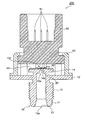
- FIG. 1 is a schematic sectional view showing an embodiment of a physical quantity measuring device according to the present invention.
- the circuit diagram of the physical quantity measuring apparatus shown in FIG. The expanded sectional view of the joining layer vicinity of the physical quantity measuring apparatus shown in FIG.
- the graph which shows an example of the typical DTA curve of glass.
- the flowchart which shows an example of the manufacturing method of the physical quantity measuring device of this embodiment.
- the flowchart which shows the modification of the manufacturing method of the physical quantity measuring apparatus shown in FIG.
- FIG. 1 is a schematic cross-sectional view showing an embodiment of a physical quantity measuring device 200 and a physical quantity measuring element 100 according to the present invention.
- a physical quantity measuring device 200 shown in FIG. 1 is a pressure measuring device that is mounted on a vehicle, for example, and measures pressures such as engine fuel pressure, brake hydraulic pressure, and various gas pressures as physical quantities. That is, the physical quantity measuring device 200 of this embodiment includes a pressure measuring element that measures pressure as the physical quantity measuring element 100.
- the physical quantity measuring device and the physical quantity measuring element according to the present invention are not limited to the pressure measuring apparatus and the pressure measuring element, and based on the stress acting on the base, for example, the physical quantity such as mass, acceleration, force, pressure, etc. Includes various devices and elements to measure.
- the physical quantity measuring apparatus 200 includes, for example, a metal casing 10, a strain detection element 30 fixed to the metal casing 10 via a bonding layer 20, and the strain detection element. 30, a cover 50 that covers the substrate 40 and the strain detection element 30, and a connector 60 that is fixed to the cover 50.
- the physical quantity measuring element 100 used in the physical quantity measuring apparatus 200 of the present embodiment includes a bonding layer 20 and a strain detecting element 30.
- the metal casing 10 includes a hollow cylindrical pressure port 11 and a flange portion 12 projecting radially from the outer periphery of the pressure port 11.
- One end of the pressure port 11 in the axial direction is a pressure introducing portion 13 opened by a pressure introducing port 13 a, and the other end in the axial direction is closed by an end wall 14.
- a mountain 15 is formed.
- the end wall 14 of the pressure port 11 has, for example, a rectangular recess 14a formed at the center of the inner wall surface, and a rectangular diaphragm 14b formed at the bottom of the recess 14a.
- the diaphragm 14b is a thin-walled portion provided at the bottom of the recess 14a of the end wall 14, and is deformed by the pressure of the fluid introduced into the pressure port 11, and for example, a strain difference between the orthogonal X direction and Y direction occurs.
- a strain detection element 30 is bonded to a portion of the outer wall surface of the end wall 14 corresponding to the diaphragm 14 b via a bonding layer 20.
- the flange portion 12 is, for example, a circular plate-like portion that is connected to the outer peripheral surface of the pressure port 11 and protrudes in the radial direction of the pressure port 11.
- the flange portion 12 is joined to the lower end portion of the cover 50 by welding, for example, and forms a space for accommodating the strain detection element 30 and the substrate 40 together with the cover 50 and the connector 60.
- the strain detection element 30 is joined to substantially the center of the outer wall surface of the end wall 14 of the pressure port 11 that is the sensor mounting surface.
- the strain detection element 30 is a semiconductor chip including one or more strain resistance bridges that output an electrical signal corresponding to deformation, ie, strain, of the diaphragm 14b of the metal housing 10 on a silicon chip.
- the end wall 14 of the pressure port 11 of the metal housing 10 is a base for joining the strain detection element 30 that is a semiconductor chip through the joining layer 20.
- the physical quantity measuring device 200 and the physical quantity measuring element 100 detect the strain of the diaphragm 14b as the base by the strain detecting element 30 as the semiconductor chip, and apply the stress acting on the diaphragm 14b as the base. Based on this, the pressure which is the physical quantity of the fluid introduced into the pressure port 11 is measured.
- the physical quantity measuring device 200 and the physical quantity measuring element 100 of the present embodiment are characterized by a bonding layer 20 that joins the strain detection element 30 that is a semiconductor chip to the end wall 14 that is a base. Details of the bonding layer 20 will be described later.
- the substrate 40 is fixed to a portion of the end wall 14 of the pressure port 11 of the metal housing 10 except for the central portion of the outer wall surface, and fixed to the central portion of the outer wall surface via the bonding layer 20 by, for example, wire bonding.
- the strain detection element 30 is connected.
- the substrate 40 includes, for example, an amplifier that amplifies each detection signal output from the strain detection element 30, an AD converter that converts an analog output signal of the amplifier into a digital signal, and a correction described later based on the digital signal.
- a digital signal calculation processing circuit for performing calculations, a memory storing various data, a capacitor, and the like are mounted.
- the cover 50 is a cylindrical member having a substantially circular opening at one end and the other end in the axial direction, and the outer shape of the intermediate portion in the axial direction is formed in, for example, a hexagonal bolt shape.
- the opening edge at the lower end of the cover 50 is bent, for example, outward in the radial direction, is in contact with the upper surface of the outer edge portion of the flange portion 12 of the metal housing 10, and is joined to the outer edge portion of the flange portion 12 by, for example, welding.
- the opening edge at the upper end of the cover 50 is, for example, caulked inward in the radial direction, and is fixed to a part of the connector 60 inserted into the cover 50 from the opening at the upper end of the cover 50.
- the connector 60 is made of, for example, resin, and has a metal needle-like terminal 61 integrated by insert molding and connected to the substrate.
- the connector 60 has, for example, three terminals 61 for power supply, grounding, and signal output.
- the physical quantity measuring device 200 is connected to be able to output a signal of a physical quantity measured to an ECU (Electronic Control Unit) of an automobile by connecting the connector 60 to, for example, an end connector of a wiring (not shown).
- ECU Electronic Control Unit
- FIG. 2 is a circuit diagram of the physical quantity measuring apparatus 200 shown in FIG.
- the strain detection element 30 includes, for example, a plurality of strain resistance bridges 31, 32, and 33.
- the substrate 40 includes, for example, a plurality of amplifiers 41, 42, and 43 that amplify output signals of the respective strain resistance bridges 31, 32, and 33, and A / D (analog / digital) conversion of outputs from the amplifiers 41, 42, and 43.
- DSP digital signal processor
- the strain resistance bridges 31, 32, and 33 are configured by bridge-connecting strain gauges that change in resistance value by distorting according to the deformation of the diaphragm 14 b of the end wall 14 of the metal casing 10 that is a base.
- the output signals of the strain resistance bridges 31, 32, 33 that is, the bridge signals based on the stress acting on the diaphragm 14b due to the pressure introduced to the pressure port 11, are amplified by the amplifiers 41, 42, 43, and further, the A / D converter. 44, 45 and 46 are converted into digital signals. Power is supplied from the voltage source E to the strain resistance bridges 31, 32, and 33 through the terminal 61 of the connector 60.
- the DSP 47 corrects the output signal based on the output signals of the distortion resistance bridges 31, 32, and 33 output from the A / D converters 44, 45, and 46, and calculates the physical quantity based on the corrected output signal.
- the measured values of the physical quantity measuring device 200 and the physical quantity measuring element 100 are output. More specifically, for example, arithmetic processing for correcting the output signal of one strain resistance bridge 31 with the output signals of the other strain resistance bridges 32 and 33 is performed, and the pressure value based on the corrected output signal is used as a measurement value. Output.
- the correction calculation may be performed by an analog circuit instead of the DSP 47.
- the DSP 47 is not limited to the correction calculation process described above.
- the DSP 47 compares the output values of the plurality of strain resistance bridges 31, 32, 33, and outputs the output values of the strain resistance bridges 31, 32, 33 to the nonvolatile memory 48 in advance. Comparison with the output value at the stored specified pressure value is performed to determine the deterioration of the measurement target device and the strain detection element 30.
- the DSP 47 also performs processing such as outputting a failure signal, for example, when determining whether the measurement target device or the strain detection element 30 is deteriorated.
- the signal output from the DSP 47 is performed via the terminal 61 of the connector 60.
- the nonvolatile memory 48 stores in advance the output values of the strain resistance bridges 31, 32, 33 when a fluid having a known pressure is introduced into the pressure port 11, for example.
- the nonvolatile memory 48 may be mounted on a circuit chip different from other circuit components.
- the bonding layer 20 which is a characteristic part of the physical quantity measuring device 200 and the physical quantity measuring element 100 of the present embodiment will be described in detail.
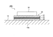
- FIG. 3 is an enlarged sectional view of the vicinity of the bonding layer 20 of the physical quantity measuring device 200 and the physical quantity measuring element 100 shown in FIG.
- the physical quantity measuring device 200 of the present embodiment is a strain detection that is a semiconductor chip that measures a physical quantity based on the end wall 14 of the metal casing 10 that is a base and the stress acting on the base.
- An element 30 and a bonding layer 20 for bonding the semiconductor chip to a base are provided.
- the physical quantity measuring element 100 of the present embodiment includes a strain detection element 30 that is a semiconductor chip that measures a physical quantity based on a stress acting on a base, and a bonding layer 20 that joins the semiconductor chip to the base. I have.
- the bonding layer 20 includes a first bonding layer 21 bonded to the strain detection element 30 that is a semiconductor chip, a second bonding layer 22 bonded to the end wall 14 of the metal housing 10 that is a base, and a first bonding layer 20. And an insulating base material 23 disposed between the bonding layer 21 and the second bonding layer 22.
- the first bonding layer 21 and the second bonding layer 22 include glass, and the thermal expansion coefficient of the first bonding layer 21 is the thermal expansion coefficient of the second bonding layer 22.
- the softening point of the first bonding layer 21 is equal to or lower than the heat resistant temperature of the semiconductor chip, and the softening point of the second bonding layer 22 is equal to or lower than the softening point of the first bonding layer 21.
- the material of the metal housing 10 including the end wall 14 as a base, high resistance to corrosion and high pressure is required, so for example, stainless steel such as SUS630 or SUS430 is used. be able to.
- a material of the strain detection element 30 as a semiconductor chip for example, silicon can be used as a material of the strain detection element 30 as a semiconductor chip.
- the thermal expansion coefficient of silicon is, for example, 37 ⁇ 10 ⁇ 7 / ° C.
- the thermal expansion coefficient of stainless steel is, for example, 113 ⁇ 10 ⁇ 7 / ° C. Therefore, there is a problem of poor bonding due to a difference in thermal expansion coefficient between the end wall 14 of the metal casing 10 as a base and the strain detection element 30 as a semiconductor chip.
- the thermal expansion coefficient is a thermal expansion coefficient in a temperature range of 50 ° C. or more and 250 ° C. or less.
- the thermal expansion coefficient of the strain detection element 30 which is a semiconductor chip is ⁇ 1
- the thermal expansion coefficient of the first bonding layer 21 is ⁇ 2
- the thermal expansion coefficient of the insulating base material 23 is ⁇ 3
- the thermal expansion coefficient of the second bonding layer 22 is It is preferable to satisfy the relationship of ⁇ 1 ⁇ 2 ⁇ 3 ⁇ 4 ⁇ 5, where ⁇ 4 and the thermal expansion coefficient of the metal casing 10 as the base are ⁇ 5.
- the thermal expansion coefficient of the bonding layer 20 is a value between the thermal expansion coefficients of the semiconductor chip and the base bonded via the bonding layer 20, and the thermal expansion coefficient of the bonding layer 20 is the thermal expansion coefficient.
- the thermal expansion coefficient of the first bonding layer 21 is equal to or lower than the thermal expansion coefficient of the second bonding layer 22, and the end wall 14 of the metal housing 10 as a base and the strain detection element 30 as a semiconductor chip It is possible to efficiently relieve the thermal stress caused by the difference in thermal expansion coefficient between the two, suppress the bonding failure between the base and the semiconductor chip, and improve the bonding stability and reliability.
- composition of the glass contained in the 1st joining layer 21 and the 2nd joining layer 22 is illustrated.
- the composition of the glass contained in the first bonding layer 21 and the second bonding layer 22 for example, a glass composition mainly containing V 2 O 5 and TeO 2 or a glass composition mainly containing PbO is used. it can. That is, the glass contained in the first bonding layer 21 and the second bonding layer 22 can contain vanadium (V).
- the main component of the glass composition refers to the one having the highest content when the glass composition is converted into an oxide.
- the glass contained in the first bonding layer 21 and the second bonding layer 22 is made into a lead-free glass composition in consideration of the environment.
- a low-melting glass having a temperature of not higher than 0 ° C. can be obtained.
- the softening points of the first bonding layer 21 and the second bonding layer 22 are set to be equal to or lower than the heat resistance temperature of the strain detection element 30 that is a semiconductor chip, and the strain detection element 30 is placed on the metal casing that is the base via the bonding layer 20. It becomes possible to join to the end wall 14 of the body 10.
- the lead-free glass composition includes a composition containing prohibited substances in the RoHS (Restriction of Hazardous Substances) directive within the range of the regulation value or less.
- the heat-resistant temperature of the strain detection element 30 that is a semiconductor chip is, for example, 430 ° C. or less.
- the glass contained in the first bonding layer 21 is, for example, 40 to 50% by weight of V 2 O 5 , 20 to 30% by weight of TeO 2 , 5.8 to 15% by weight of P 2 O 5 in terms of oxidation, Fe 2 O 3 may be included in an amount of 0 to 15% by weight, WO 3 in an amount of 0 to 10% by weight, and ZnO in an amount of 0 to 10% by weight. Further, the glass desirably contains 10% by weight or more of Fe 2 O 3 . By containing 10 wt% or more of Fe 2 O 3 , it becomes possible to lower the softening point of the glass while reducing the thermal expansion coefficient of the glass mainly composed of V 2 O 5 .
- the glass composition is easily crystallized, but by containing WO 3 in the range of 0 to 10% by weight, this crystallization can be suppressed.
- the addition of ZnO can improve the adhesion between the SiO 2 -based glass.
- the glass contained in the second bonding layer 22 is, in terms of oxidation, 37.2 to 50% by weight of V 2 O 5 , 20 to 30% by weight of TeO 2 , 0 to 15% by weight of P 2 O 5 , Fe 2 O 3 may be included in an amount of 0 to 15 wt%, WO 3 may be included in an amount of 0 to 10 wt%, BaO may be included in an amount of 0 to 26 wt%, and ZnO may be included in an amount of 0 to 10 wt%. Further, the glass may contain 0 to 5% by weight of an alkali metal oxide such as K 2 O or Cs 2 O as other components.
- the first bonding layer 21 and the second bonding layer 22 can be formed using, for example, glass paste.
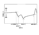
- FIG. 4 is a graph showing an example of a typical DTA curve of glass.
- Characteristic temperatures such as glass transition temperature Tg, yield point Td, softening point Ts, and crystallization temperature Tc of the glass contained in the first bonding layer 21 and the second bonding layer 22 are, for example, differential thermal analysis (Differential Thermal Analysis: DTA).
- DTA Different Thermal Analysis
- the softening point Ts of glass is the second endothermic peak in the DTA curve, as shown in FIG.
- the first bonding layer 21 and the second bonding layer 22 may include a filler material having a smaller coefficient of thermal expansion than the glass included in the first bonding layer 21 and the second bonding layer 22, for example.
- the content rate of the filler material of the first bonding layer 21 is set higher than the content rate of the filler material of the second bonding layer 22.
- filler material examples include zircon, zirconia, quartz glass, ⁇ -spongeumen, cordierite, mullite, ⁇ -eucryptite, ⁇ -quartz, zirconium phosphate, zirconium tungstate phosphate (ZWP), and zirconium tungstate. , And solid solutions of these materials can be used, or one or more of these materials can be used in combination.
- the content of the filler material of the first bonding layer 21 is, for example, 30% by volume or more and 40% by volume or less, and more preferably 35% by volume or more and 40% by volume or less. Further, the content of the filler material of the second bonding layer 22 is not particularly limited as long as it is less than the content of the filler material of the first bonding layer 21. Thereby, the thermal expansion coefficients of the first bonding layer 21 and the second bonding layer 22 are adjusted to a thermal expansion coefficient suitable for bonding between the semiconductor chip and the base having a large difference in thermal expansion coefficient, for example, as described above. be able to.
- the thermal expansion coefficient of the first bonding layer 21 can be adjusted to, for example, 42 ⁇ 10 ⁇ 7 / ° C. or more and 62 ⁇ 10 ⁇ 7 / ° C. or less, and more preferably 42 ⁇ 10 ⁇ 7 / ° C. or more and 50 ⁇ . It can be adjusted to 10 ⁇ 7 / ° C. or less.
- the thermal expansion coefficient of the second bonding layer 22 can be adjusted to, for example, 42 ⁇ 10 ⁇ 7 / ° C. or more and 113 ⁇ 10 ⁇ 7 / ° C. or less, and more preferably 67 ⁇ 10 ⁇ 7 / ° C. or more and 102 ⁇ . It can be adjusted to 10 ⁇ 7 / ° C. or less.
- the insulating base material 23 is not particularly limited as long as it is a material having electrical insulation properties.
- a general high-resistance material such as glass, silicon, or alumina can be used.
- the glass used as the insulating base material 23 is, for example, a high-resistance glass mainly composed of SiO 2 .
- the volume resistivity of the insulating base material 23 is preferably, for example, 10 10 ⁇ cm or more.
- the bonding layer 20 includes the insulating base 23 having such an insulating property, electrical noise from the metal housing 10 which is a base of the physical quantity measuring device 200 to the strain detecting element 30 which is a semiconductor chip is cut off. In addition, noise included in the output of the strain detection element 30 can be suppressed. Moreover, it is preferable that the insulation base material 23 is lead-free on the restrictions in RoHS directive.
- the thermal expansion coefficient of the insulating base material 23 is, for example, not less than 38 ⁇ 10 ⁇ 7 / ° C. and not more than 100 ⁇ 10 ⁇ 7 / ° C. Thereby, the joining reliability between the insulating base material 23 and the 1st joining layer 21 and the 2nd joining layer 22 can be improved.
- the thermal expansion coefficient of the insulating base material 23 is 66 ⁇ 10 ⁇ 7 / ° C. or more and 84 ⁇ 10 ⁇ 7 / ° C. or less. Preferably it is.
- the thickness of the insulating base material 23 is, for example, 5 ⁇ m or more and 500 ⁇ m or less, it is possible to ensure insulation reliability and suppress noise.
- the thickness of the insulating base material 23 is preferably 20 ⁇ m or more and 100 ⁇ m or less from the viewpoint of improving the insulation reliability, further suppressing noise, and reducing the thickness of the insulating layer.
- the end wall 14 of the metal casing 10 that is a base and the strain detection element 30 that is a semiconductor chip are selected from the group consisting of Al, Ni, Ti, and Mo on the surface to which the bonding layer 20 is bonded. It is preferable to have a metal film containing at least one kind.
- a method for forming a metal film on the surface to which the bonding layer 20 is bonded by performing metallization is not particularly limited, and for example, a plating method, a sputtering method, or a vapor deposition method can be used.
- the physical quantity measuring device 200 is a strain detection that is a semiconductor chip that measures a physical quantity based on the end wall 14 of the metal casing 10 that is a base and the stress acting on the base.
- An element 30 and a bonding layer 20 for bonding the semiconductor chip to a base are provided.
- the physical quantity measuring element 100 of the present embodiment includes a strain detection element 30 that is a semiconductor chip that measures a physical quantity based on a stress acting on a base, and a bonding layer 20 that joins the semiconductor chip to the base. I have.
- the bonding layer 20 includes a first bonding layer 21 bonded to the strain detection element 30 that is a semiconductor chip and a metal casing 10 that is a base. It has the 2nd joining layer 22 joined to the end wall 14, and the insulating base material 23 arrange
- the 1st joining layer 21 and the 2nd joining layer 22 contain glass, the thermal expansion coefficient of the 1st joining layer 21 is below the thermal expansion coefficient of the 2nd joining layer 22, and the softening point of the 1st joining layer 21 Is below the heat resistance temperature of the semiconductor chip, and the softening point of the second bonding layer 22 is below the softening point of the first bonding layer 21.
- the thermal expansion coefficient of the first bonding layer 21 is equal to or less than the thermal expansion coefficient of the second bonding layer 22, thereby causing a difference in thermal expansion coefficient between the metal base and the silicon semiconductor chip.
- the resulting stress can be relaxed and the reliability of bonding between the base and the semiconductor chip can be improved.
- the softening point of the first bonding layer 21 is lower than the heat resistance temperature of the semiconductor chip and the softening point of the second bonding layer 22 is lower than the softening point of the first bonding layer 21, the bonding temperature of the bonding layer 20 is reduced. The temperature can be lowered without affecting the operation of the semiconductor chip.
- the insulating base material 23 ensures the insulation between the semiconductor chip and the base and reduces noise with respect to the input / output of the semiconductor chip. be able to.
- the semiconductor chip can be bonded to the base using the solid bonding layer 20, it is not necessary to use a printing method when bonding the semiconductor chip to the base, and the semiconductor chip mounting surface. It is freed from the constraints on the base, and the joining reliability can be improved. Further, when the softening point of the second bonding layer 22 is lower than the softening point of the first bonding layer 21 by, for example, 7 ° C. or more, the warping of the bonding layer 20 can be reduced and the bonding reliability can be improved. it can.
- the physical quantity measuring device 200 and the physical quantity measuring element 100 that can improve the bonding reliability between the base and the semiconductor chip and the reliability of the operation of the semiconductor chip. it can.
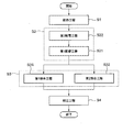
- FIG. 5 is a flowchart showing an example of a manufacturing method of the physical quantity measuring device 200 of the present embodiment shown in FIG.
- the manufacturing method of the physical quantity measuring device 200 according to the present embodiment includes, for example, a manufacturing process S1 for manufacturing a component, an arrangement process S2 for arranging the bonding layer 20, and a strain detection element 30 that is a semiconductor chip by the bonding layer 20.
- the parts constituting the physical quantity measuring device 200 such as the metal casing 10, the bonding layer 20, the strain detecting element 30, the substrate 40, the cover 50, the connector 60, and the like are manufactured.
- Components other than the bonding layer 20 can be manufactured in the same manner as in the past.
- the bonding layer 20 can be manufactured, for example, by applying a glass paste for forming the first bonding layer 21 and the second bonding layer 22 to the insulating base material 23 and baking it.
- a glass paste for forming the first bonding layer 21 is applied to one surface of the insulating base material 23 and dried, and then the insulating base material 23 is formed.
- a glass paste for forming the second bonding layer 22 is applied to the other surface of 23 and dried.
- a glass paste what knead
- the glass used for the glass paste is prepared by adding a raw material in which an oxide corresponding to the composition of the glass is mixed and mixed into a platinum crucible, and heating it to 800 to 1100 ° C. at a heating rate of 5 to 10 ° C./min in an electric furnace. It can be produced by maintaining the temperature over time. While heating the raw material and maintaining the temperature, it is desirable to stir to make the glass uniform. Also, when taking out the crucible from the electric furnace and taking out the glass from the crucible, in order to prevent moisture adsorption on the glass surface, the glass is placed on a graphite mold or stainless steel plate heated to about 100 to 150 ° C. in advance. It is desirable to pour.
- a solvent used for the glass paste for example, butyl carbitol acetate or ⁇ -terpineol can be used.
- a binder used for glass paste ethyl cellulose, nitrocellulose, etc. can be used, for example.
- the first bonding layer 21 and the second bonding layer 22 are temporarily fired by performing binder removal processing and temporary firing of the glass paste applied to both surfaces of the insulating base material 23 and cutting to a desired size.
- the bonded layer 20 can be obtained. With such a manufacturing method, mass production of the bonding layer 20 can be performed, and the manufacturing cost can be reduced.
- the glass binder applied to the insulating base material 23 may be omitted from the binder treatment and temporary baking.
- the first bonding layer 21 and the second bonding layer 22 may be formed by performing binder removal processing, temporary baking, and main baking of the glass paste applied to the insulating base material 23. it can.
- the second placement step of placing the joining layer 20 with the second joining layer 22 facing the central portion where the diaphragm 14b of the end wall 14 of the metal casing 10 as the base is formed.
- S22 is performed.
- a first placement step S21 for placing the strain detection element 30 that is a semiconductor chip opposite to the first joining layer 21 of the joining layer 20 that is placed on the end wall 14 of the metal housing 10 that is the base is performed.
- the second bonding layer 22 of the bonding layer 20 is used as a base metal housing after the first placement step S21 in which the strain detection element 30 that is a semiconductor chip is disposed so as to face the first bonding layer 21 of the bonding layer 20.
- the first joining step S31 and the second joining step S32 are performed. carry out.
- the bonding layer 20 is heated to a temperature not lower than the softening point of the first bonding layer 21 and not higher than the heat resistance temperature of the semiconductor chip, and the semiconductor chip and the bonding layer 20 are connected via the first bonding layer 21. Join.
- the bonding layer 20 is heated to a temperature not lower than the softening point of the second bonding layer 22 and not higher than the heat resistance temperature of the semiconductor chip, and the base and the bonding layer 20 are connected via the second bonding layer 22. Join.
- the bonding layer 20 is equal to or higher than the softening point of the first bonding layer 21 and the heat resistant temperature of the semiconductor chip.
- the first bonding step S31 and the second bonding step S32 can be performed collectively by heating to the following temperature.
- the substrate 40 is fixed to the end wall 14 of the metal casing 10 to which the strain detection element 30 that is a semiconductor chip is bonded via the bonding layer 20, and the terminals of the strain detection element 30 are formed by wire bonding, for example. And a terminal of the substrate 40 are connected.
- the connector 60 is fixed to the cover 50, the terminal 61 of the connector 60 is connected to the terminal of the substrate 40, and the cover 50 and the flange portion 12 of the metal housing 10 are joined by welding, for example.
- the physical quantity measuring device 200 of the present embodiment can be manufactured.
- the thermal expansion coefficient of the first bonding layer 21 is equal to or lower than the thermal expansion coefficient of the second bonding layer 22, so that the heat between the base and the semiconductor chip is increased. It is possible to relieve the stress caused by the difference in expansion coefficient and improve the bonding reliability between the base and the semiconductor chip.
- the softening point of the first bonding layer 21 is lower than the heat resistance temperature of the semiconductor chip and the softening point of the second bonding layer 22 is lower than the softening point of the first bonding layer 21, the bonding temperature of the bonding layer 20 is reduced. The temperature can be lowered without affecting the operation of the semiconductor chip.
- the insulating base material 23 ensures the insulation between the semiconductor chip and the base and reduces noise with respect to the input / output of the semiconductor chip. be able to.
- the semiconductor chip can be bonded to the base using the solid bonding layer 20, it is not necessary to use a printing method when bonding the semiconductor chip to the base, and the semiconductor chip mounting surface. It is free from constraints such as the shape of the base, and the joining reliability can be improved. Further, when the softening point of the second bonding layer 22 is lower than the softening point of the first bonding layer 21 by, for example, 7 ° C. or more, the warping of the bonding layer 20 can be reduced and the bonding reliability can be improved. it can.
- FIG. 6 is a flowchart showing a modification of the manufacturing method of the physical quantity measuring device 200 shown in FIG.
- the manufacturing method of the physical quantity measuring device according to the present invention is not limited to the embodiment shown in FIG. 5, and can also be implemented by the embodiment shown in FIG. 6.
- the bonding layer 20 is softened to the first bonding layer 21.
- the case where the first bonding step S31 and the second bonding step S32 are performed collectively by heating to a temperature not lower than the point and not higher than the heat resistant temperature of the semiconductor chip has been described.
- the first arrangement process S ⁇ b> 21 is performed in which the semiconductor chip and the first bonding layer 21 of the bonding layer 20 are arranged to face each other.
- the bonding layer 20 is heated to a temperature equal to or higher than the softening point of the first bonding layer 21 and equal to or lower than the heat resistance temperature of the semiconductor chip, thereby bonding the semiconductor chip and the bonding layer 20 via the first bonding layer 21.
- the joining step S31 is performed. Thereby, as shown in FIG. 3, the physical quantity measuring element 100 including the strain detecting element 30 and the bonding layer 20 which are semiconductor chips can be manufactured.
- a second placement step S22 is performed in which the base and the second joining layer 22 of the joining layer 20 are placed facing each other.
- the bonding layer 20 is heated to a temperature equal to or higher than the softening point of the second bonding layer 22 and equal to or lower than the heat resistance temperature of the semiconductor chip to bond the base and the bonding layer 29 via the second bonding layer 22.
- the joining step S32 is performed. At this time, since the softening point of the second bonding layer 22 is lower than the softening point of the first bonding layer 21, bonding is performed via the second bonding layer 22 while maintaining the bonding between the first bonding layer 21 and the semiconductor chip. Layer 20 can be bonded to the base.
- glass As raw materials for glass, vanadium pentoxide, tellurium oxide, ferric oxide, phosphorus pentoxide, tungsten oxide, barium carbonate, antimony oxide, barium phosphate, potassium carbonate, bismuth oxide, boron oxide, zinc oxide, copper oxide are used. Glasses G1 to G13 having the compositions shown in Table 1 below were produced. In the glass composition shown in Table 1, all components are expressed in mass percent in terms of oxide.
- Glass G1-G13 was produced according to the following procedure. First, 1 kg of mixed powder prepared by mixing and mixing the raw materials so as to have the composition shown in Table 1 is placed in a platinum crucible and heated to a heating temperature of 1000 to 1200 ° C. at a heating rate of 5 to 10 ° C./min using an electric furnace. And held for 2 hours. While maintaining the heating temperature, stirring was performed to obtain a uniform glass. Next, the platinum crucible was taken out from the electric furnace, and the molten glass was poured onto a stainless steel plate heated to 100 ° C. in advance to obtain glasses G1 to G13.
- the glass paste for forming the 1st joining layer and the 2nd joining layer of a joining layer was produced.
- the glasses G1 to G13 were individually pulverized using a jet mill until the average particle diameter (D50) became about 3 ⁇ m to obtain the glass G1 to G13 powders.
- the obtained glass G1 to G13 powder has Zr 2 (WO 4 ) (PO 4 ) 2 (hereinafter sometimes abbreviated as ZWP) having an average particle diameter (D50) of about 3 ⁇ m as a filler material,
- a predetermined amount of cordierite (hereinafter sometimes abbreviated as CRD) or aluminum (Al) was added to obtain a mixed powder.
- glass powder was prepared by adding ethyl cellulose as a binder and butyl carbitol acetate as a solvent to the mixed powder obtained by adding glass G1 to G13 powder or filler material, and kneading them.
- a thin glass plate having a thickness of 30 ⁇ m and a thermal expansion coefficient of 66 ⁇ 10 ⁇ 7 / ° C. was prepared as an insulating base material for the bonding layer.
- the glass paste is similarly applied to the other surface of the insulating base material and dried. I let you.
- the insulating base material coated with the glass paste was heated at 330 ° C. for 30 minutes.
- the insulating base material coated with the glass paste is temporarily fired at the same temperature as the bonding temperature of the bonding layer, whereby the first bonding layer bonded to the semiconductor chip and the second bonding bonded to the base
- positioned between the 1st joining layer and the 2nd joining layer was obtained.
- the thickness of each obtained bonding layer was approximately 90 ⁇ m.
- Table 3 shows the types of glass contained in the first bonding layer and the second bonding layer of each of the bonding layers of Comparative Examples C1 to C11, the content [volume%], and the types of filler materials contained. And its content [volume%], thermal expansion coefficient [10 ⁇ 7 / ° C.], and softening point [° C.].
- the glass type is the glass No. shown in Table 1. Is shown.
- the measurement of the thermal expansion coefficient of the 1st joining layer of each joining layer shown in Table 2 and Table 3 and the 2nd joining layer was performed as follows. First, glass powder not containing a binder and a solvent or a mixed powder of glass powder and filler material was uniaxially pressed, and then densely baked in an electric furnace and cut to obtain a test piece. The dimension of the test piece was 4 mm ⁇ 4 mm ⁇ 15 mm. Using the test piece, a thermal expansion coefficient in the range of 50 to 250 ° C. was measured using a push rod thermomechanical analyzer.
- the softening points of the first bonding layer and the second bonding layer of each bonding layer shown in Table 2 and Table 3 were determined as follows. First, differential thermal analysis (DTA) was performed on the above glass powder or mixed powder at a rate of temperature increase of 5 ° C./min. Alumina powder was used as a standard sample. In the obtained DTA curve, the second endothermic peak temperature was defined as the softening point Ts.
- DTA differential thermal analysis
- a semiconductor chip (4 mm ⁇ 4 mm, 37 ⁇ 10 ⁇ 7 / ° C.) in which an Al film was formed by metallizing the bonding surface was prepared as a semiconductor chip used in the physical quantity measuring apparatus.
- a diaphragm ( ⁇ 12 mm, coefficient of thermal expansion: 113 ⁇ 10 ⁇ 7 / ° C.) made of stainless steel (SUS630) was prepared as a base for joining the semiconductor chips via the joining layer.
- each bonding layer was heated to a temperature bonding temperature equal to or higher than the softening point of the first bonding layer, and the semiconductor chip was bonded to the base via the bonding layer.
- Table 4 shows the bonding temperatures of the bonding layers of Examples E1 to E18, and the evaluation results of adherability / reliability, reliability, and chip operation.
- Table 5 shows the bonding temperature of the bonding layers of Comparative Examples C1 to C11, and the evaluation results of adherability / reliability, reliability, and chip operation.
- Tables 4 and 5 The reliability shown in Tables 4 and 5 was evaluated by performing a temperature cycle test and a shear strength test at ⁇ 40 ° C. to 150 ° C. on the semiconductor chip and the base bonded through the bonding layer. As a result, all samples were evaluated as good ( ⁇ ) when no problem occurred. Also, depending on the sample, cracking or peeling of the semiconductor chip may occur or the bonding strength may vary widely. However, a sample containing many samples with no problem is evaluated as acceptable ( ⁇ ). The case where peeling occurs and the case where the bonding strength is 10 Mpa or less were evaluated as impossible (x).
- the evaluation of the chip operation shown in Table 4 and Table 5 is performed by manufacturing the physical quantity measuring device of the above-described embodiment shown in FIG. 1 using a semiconductor chip bonded to a diaphragm as a base through each bonding layer.
- the evaluation was performed by evaluating the operation of the strain detection element which is a semiconductor chip.
- the physical quantity measuring apparatus was evaluated as good ( ⁇ ) when the malfunction was less than 1%, acceptable ( ⁇ ) when it was less than 10%, and impossible ( ⁇ ) when it was 50% or more.
- the thermal expansion coefficient of the first bonding layer is not more than the thermal expansion coefficient of the second bonding layer
- the softening point of the first bonding layer is not more than the heat resistant temperature of the semiconductor chip (for example, 430 ° C.)
- the thermal expansion coefficient of the first bonding layer is preferably 42 ⁇ 10 ⁇ 7 / ° C. or more and 62 ⁇ 10 ⁇ 7 / ° C. or less
- the thermal expansion coefficient of the second bonding layer is 42 ⁇ 10 7 -7 / ° C. or higher and 113 ⁇ 10 ⁇ 7 / ° C. or lower were good.
- the thermal expansion coefficient of the first bonding layer is 42 ⁇ 10 ⁇ 7 / ° C. or more and 50 ⁇ 10 ⁇ 7 / ° C. or less
- the thermal expansion coefficient of the second bonding layer is 67 ⁇ 10 ⁇ 7 / ° C. or more and 102
- ⁇ 10 ⁇ 7 / ° C. or lower a physical quantity measuring apparatus excellent in both the bonding state and bonding reliability between the semiconductor chip and the base was obtained.
- the relationship of the thermal expansion coefficient ⁇ is that the thermal expansion coefficient of the strain detecting element is ⁇ 1 , the thermal expansion coefficient of the bonding layer on the upper surface is ⁇ 2, and the thermal expansion coefficient of the insulating substrate is ⁇ 3.
- the relationship of ⁇ 1 ⁇ 2 ⁇ 3 ⁇ 4 ⁇ 5 was satisfied, where ⁇ 4 was the thermal expansion coefficient of the bonding layer on the lower surface and ⁇ 5 was the thermal expansion coefficient of the diaphragm.
- the glass composition contained in the first bonding layer is 40 to 50% by weight of V 2 O 5 , 20 to 30% by weight of TeO 2 , and 5.8 to 15% by weight of P 2 O 5. %, Fe 2 O 3 is 0 to 15% by weight, WO 3 is 0 to 10% by weight, and ZnO is 0 to 10% by weight.
- the composition of the glass contained in the second bonding layer is V 2 O 5 37.2-50% by weight, TeO 2 20-30% by weight, P 2 O 5 0-15% by weight, Fe 2 O 3 0-15% by weight, WO 3 0-10% by weight, BaO Was 0 to 26% by weight, and ZnO was in the range of 0 to 10% by weight. Further, it contained 0 to 5% by weight of K 2 O or Cs 2 O alkali metal oxide as other components.
- the softening point of the second bonding layer was 7 ° C. or more lower than the softening point of the first bonding layer, the warping of the bonding layer was small. Although this is considered to be due to the fixing temperature of the glass, it has been found that it is more preferable from the viewpoint of handling the bonding layer.
- Example E21 a commercially available lead-based glass paste AGC made at 430 ° C. for bonding at a thermal expansion coefficient of 72 ⁇ 10 ⁇ 7 / ° C. was used as the material for the second bonding layer.
- the configurations of the first bonding layer and the second bonding layer of each bonding layer are shown in Table 6 below.
- the bonding temperature of the bonding layer is equal to or lower than the heat resistant temperature of the semiconductor chip (for example, 430 ° C.), the bonding state and bonding reliability are good ( ⁇ ), and the chip operation is also possible ( ⁇ ).
- the bonding temperature of the bonding layer is preferably equal to or lower than the heat resistant temperature of the semiconductor chip.
- the bonding temperature of the bonding layer is a temperature equal to or higher than the softening point of the first bonding layer of the bonding layer or higher than the softening point of the first bonding layer.
- bonding layers of Examples E22 to E33 were prepared in the same manner as Example E10 except for the configuration of the insulating substrate. And the physical quantity measuring apparatus was produced using each produced joining layer.
- a bonding layer of Comparative Example C12 having the same first bonding layer and second bonding layer as in Example E10 and having no insulating substrate was produced. Specifically, first, a glass paste for forming the second bonding layer was applied onto a diaphragm as a base, dried, and pre-baked. Thereafter, a glass paste for forming the first bonding layer was applied onto the pre-fired second bonding layer, dried, and pre-baked. Thereafter, the semiconductor chip was placed on the pre-fired first bonding layer and heated at 400 ° C. Thereby, the semiconductor chip was bonded to the base via the bonding layer of Comparative Example C12, and a physical quantity measuring device was manufactured.
- Examples E22 to E33 and Comparative Example C12 were evaluated in the same manner as in Examples E1 to E21 described above.
- Table 8 below shows the configuration of the insulating base material of the bonding layers of Examples E22 to E33 and Comparative Example C12, the bonding temperature, and the evaluation results of adherability / reliability, reliability, and chip operation.
- insulating base material As an insulating base material, it was confirmed that it can be used if it is a general high resistance material such as Si or alumina in addition to glass mainly composed of SiO 2 .
- the linear thermal expansion coefficient of the insulating substrate was found to be widely usable from 38 ⁇ 10 ⁇ 7 / ° C. to 100 ⁇ 10 ⁇ 7 / ° C., but the linear thermal expansion coefficient with the first and second bonding layers From this relationship, it was found that the range of 66 ⁇ 10 ⁇ 7 / ° C. or higher and 84 ⁇ 10 ⁇ 7 / ° C. or lower is particularly preferable.
- the thickness of the insulating base material can be widely used from about 5 ⁇ m to about 500 ⁇ m, it was found that the thickness is particularly preferably 20 ⁇ m or more from the viewpoint of reliability. However, since the output as the physical quantity measuring device is reduced when the thickness of the insulating base is increased, the particularly preferable thickness of the insulating base is 20 ⁇ m or more and 100 ⁇ m or less.
- the effect of the metal film formed on the surface where the bonding layer of the base is bonded was verified.
- a stainless steel (SUS630) diaphragm was used as a base, and a pretreatment of Ni plating and Al sputtering was performed on the joint surface of the base to which the joint layer was joined to form a metal film.
- the physical quantity measuring apparatus was produced using the joining layer of Examples E1 to E18. As a result, it was found that the shear bonding strength was improved in any of the bonding layers of Examples E1 to E18. For this reason, it is desirable to pre-treat the bonding surface of the base to form a metal film containing at least one selected from the group consisting of Al, Ni, Ti, and Mo.
Landscapes
- Physics & Mathematics (AREA)
- General Physics & Mathematics (AREA)
- Chemical & Material Sciences (AREA)
- Analytical Chemistry (AREA)
- Measuring Fluid Pressure (AREA)
- Pressure Sensors (AREA)
- Testing Or Calibration Of Command Recording Devices (AREA)
Abstract
接合層の接合温度を半導体チップの動作に影響のない温度に低下させ、半導体チップと基台との絶縁性を確保した物理量測定装置を提供する。 基台(ダイアフラム14b)と、該基台に作用する応力に基づいて物理量を測定する半導体チップ(歪検出素子30)と、該半導体チップを基台に接合する接合層20とを備える物理量測定装置。接合層20は、半導体チップに接合される第1接合層21と、基台に接合される第2接合層22と、第1接合層21と第2接合層22との間に配置された絶縁基材23と、を有する。第1接合層21および第2接合層22は、ガラスを含む。第1接合層21の熱膨張係数は、第2接合層22の熱膨張係数以下であり、第2接合層22の軟化点は、半導体チップの耐熱温度以下であり、第1接合層21の軟化点は、第2接合層22の軟化点以下である。
Description
本発明は、たとえば圧力等の物理量を測定する物理量測定装置およびその製造方法ならびに物理量測定素子に関する。
従来の物理量測定装置の一例として、測定対象の各種機器に装着されて圧力を測定する圧力測定装置が知られている(下記特許文献1を参照)。特許文献1に記載された圧力測定装置は、金属筐体と、歪検出素子とを備えている。金属筐体は、圧力導入部と、該圧力導入部から導入された圧力により変形が発生するダイアフラムとを有する。歪検出素子は、ダイアフラムに発生する歪を検出する。
前記圧力測定装置は、前記金属筐体上に第一の脆性材からなる基台を有している。前記圧力測定装置において、前記歪検出素子は、前記基台よりも低融点である第二の脆性材料を介して基台と接合される。特許文献1には、前記構成により、シリコンやガラスの熱膨張係数と比べて熱膨張係数が大きい金属材料からなるダイアフラムと歪検出素子との接合信頼性の高い圧力検出素子を提供できることが記載されている。
また、物理量測定装置の別の例として、金属ステムのダイアフラムにセンサ素子がガラス接合された圧力センサおよびその製造方法に関する発明が開示されている(下記特許文献2を参照)。特許文献2に記載された圧力センサは、金属ステムと、接合ガラスと、センサ素子とを備えている。
前記金属ステムは、圧力媒体が導入される圧力導入孔が設けられた中空円筒形状であって、該圧力導入孔の一方を閉じるように該中空円筒形状の一端部に設けられているダイアフラムを有している。このダイアフラムは、前記圧力導入孔に導入された圧力媒体の圧力によって歪む。
前記接合ガラスは、前記金属ステムの一端部のうち前記ダイアフラムにおいて前記圧力導入孔とは反対側に設けられている。前記センサ素子は、前記接合ガラスを介して前記ダイアフラムに接合され、前記ダイアフラムの歪みに応じたセンサ信号を出力する。この特許文献2に記載された圧力センサは、以下の構成に特徴を有している。
前記金属ステムは、前記ダイアフラムのうち前記接合ガラスが配置された基準面から突出するように当該金属ステムの一端部に設けられた凸部を有している。この凸部は、前記金属ステムの一端部において前記接合ガラスの周囲に位置している。この凸部の高さは、前記基準面を基準とした前記接合ガラスの厚みに対して、20%以上の高さである。
特許文献2には、前記構成により、凸部によってダイアフラムに対する接合ガラスの位置が規制され、ダイアフラムに対する接合ガラスの位置ずれを防止することができ、金属ステムのダイアフラムに対するセンサ素子の位置ずれを防止できることが記載されている。
前記特許文献1に記載の圧力測定装置では、ダイアフラムにベース基台としてガラスペーストを塗布し、ベース基台の上にトップ基台としてガラス板を搭載して焼結することで2層の脆性材からなる基台を成形している(同文献、段落0039等を参照)。ガラスペーストを使用する場合には、粘度管理が必要であり、仮焼成等の前工程が必要になるという課題がある。また、ガラスペーストは、通常、スクリーン印刷などの印刷によって塗布されるため、平坦な面以外に塗布するのが困難であるという課題がある。
一方、前記特許文献2には、粒状ガラスが成形された固形状のタブレットガラスを基準面に配置し、そのタブレットガラスの上にセンサ素子を配置し、当該タブレットガラスを焼成して接合ガラスを形成し、この接合ガラスを介してセンサ素子をダイアフラムに接合することが記載されている(同文献、段落0013および0014等を参照)。これにより、印刷を行う必要がなく、平坦な面以外にもセンサ素子を固定することができる。
前記特許文献2では、タブレットガラスとして、たとえば430℃で焼成可能な低融点ガラスを用いている(同文献、段落0037を参照)。このような低融点ガラスとしては、一般に、鉛、ビスマス、またはバナジウムを多く含むガラスが知られている。しかし、前記従来の物理量測定装置において、ダイアフラム等の基台と、該基台に作用する圧力等の物理量を測定する半導体チップとを接合する接合層として上記のような低融点ガラスを用いる場合には、以下のような課題がある。
前記接合層として、たとえば、ビスマスを多く含むガラスを使用すると、鉛やバナジウムを多く含むガラスと比較して接合温度が高くなり、半導体チップの動作に悪影響がおよぶおそれがある。また、前記接合層として、たとえば、鉛を多く含むガラスを使用すると、RoHS指令等の環境上の問題が生じるおそれがある。また、前記接合層として、たとえば、バナジウムを多く含むガラスを使用すると、前記接合層が電気伝導性を有し、半導体チップと基台との絶縁が不十分になり、ノイズが増加するおそれがある。
本発明は、前記課題に鑑みてなされたものであり、基台と半導体チップの接合信頼性および半導体チップの動作の信頼性を向上させることができる物理量測定装置およびその製造方法ならびに物理量測定素子を提供することを目的とする。
前記目的を達成すべく、本発明の物理量測定装置は、基台と、該基台に作用する応力に基づいて物理量を測定する半導体チップと、該半導体チップを前記基台に接合する接合層とを備える物理量測定装置であって、前記接合層は、前記半導体チップに接合される第1接合層と、前記基台に接合される第2接合層と、前記第1接合層と前記第2接合層との間に配置された絶縁基材と、を有し、前記第1接合層および前記第2接合層は、ガラスを含み、前記第1接合層の熱膨張係数は、前記第2接合層の熱膨張係数以下であり、前記第1接合層の軟化点は、前記半導体チップの耐熱温度以下であり、前記第2接合層の軟化点は、前記第1接合層の軟化点以下であることを特徴とする。
本発明によれば、基台と半導体チップの接合信頼性および半導体チップの動作の信頼性を向上させることができる物理量測定装置およびその製造方法ならびに物理量測定素子を提供することができる。
以下、図面を参照して本発明の物理量測定装置および物理量測定素子の実施形態を説明する。
(物理量測定装置および物理量測定素子)
図1は、本発明に係る物理量測定装置200および物理量測定素子100の一実施形態を示す概略断面図である。
図1は、本発明に係る物理量測定装置200および物理量測定素子100の一実施形態を示す概略断面図である。
図1に示す物理量測定装置200は、たとえば、車両に搭載され、物理量としてエンジンの燃料圧、ブレーキ油圧、各種ガス圧等の圧力を測定する圧力測定装置である。すなわち、本実施形態の物理量測定装置200は、物理量測定素子100として、圧力を測定する圧力測定素子を備えている。なお、本発明に係る物理量測定装置および物理量測定素子は、圧力測定装置および圧力測定素子に限定されず、基台に作用する応力に基づいて、たとえば、質量、加速度、力、圧力等の物理量を測定する各種の装置および素子を含む。
本実施形態の物理量測定装置200は、図1に示すように、たとえば、金属筐体10と、該金属筐体10に接合層20を介して固定された歪検出素子30と、該歪検出素子30に接続された基板40と、該基板40および歪検出素子30を覆うカバー50と、該カバー50に固定されたコネクタ60とを備えている。また、本実施形態の物理量測定装置200に用いられる物理量測定素子100は、接合層20と歪検出素子30とを備えている。
金属筐体10は、中空円筒状の圧力ポート11と、該圧力ポート11の外周から径方向に張り出したフランジ部12とを備えている。圧力ポート11は、その軸方向の一端が圧力導入口13aによって開放された圧力導入部13とされ、その軸方向の他端が端部壁14によって閉塞されている。圧力ポート11のフランジ部12と圧力導入口13aとの間の外周面には、圧力等の物理量を測定する測定対象の流体が流れる配管等に物理量測定装置200を締結して固定するためのねじ山15が形成されている。
圧力ポート11の端部壁14は、内壁面の中央部に、たとえば矩形の凹部14aが形成され、その凹部14aの底部に、たとえば矩形のダイアフラム14bが形成されている。ダイアフラム14bは、端部壁14の凹部14aの底部に設けられた薄肉部であり、圧力ポート11に導入された流体の圧力によって変形し、たとえば直交するX方向とY方向の歪差が生じる。端部壁14の外壁面のダイアフラム14bに対応する部分には、接合層20を介して歪検出素子30が接合されている。
フランジ部12は、たとえば、圧力ポート11の外周面に接続されて圧力ポート11の径方向に張り出した円形の板状の部分である。フランジ部12は、その周縁部が、たとえば溶接によってカバー50の下端部に接合され、カバー50およびコネクタ60とともに歪検出素子30および基板40を収容する空間を形成している。
歪検出素子30は、センサ搭載面である圧力ポート11の端部壁14の外壁面のほぼ中央部に接合されている。歪検出素子30は、シリコンチップ上に金属筐体10のダイアフラム14bの変形すなわち歪に応じた電気信号を出力する1つ以上の歪抵抗ブリッジを備える半導体チップである。
すなわち、本実施形態の物理量測定装置200において、金属筐体10の圧力ポート11の端部壁14は、接合層20を介して半導体チップである歪検出素子30を接合するための基台である。換言すると、本実施形態の物理量測定装置200および物理量測定素子100は、半導体チップとしての歪検出素子30によって基台としてのダイアフラム14bの歪を検出し、基台としてのダイアフラム14bに作用する応力に基づいて、圧力ポート11に導入された流体の物理量である圧力を測定する。
本実施形態の物理量測定装置200および物理量測定素子100は、半導体チップである歪検出素子30を、基台である端部壁14に接合する接合層20に特徴を有している。この接合層20の詳細については、後述する。
基板40は、たとえば金属筐体10の圧力ポート11の端部壁14において、外壁面の中央部を除く部分に固定され、たとえばワイヤボンディングによって、外壁面の中央部に接合層20を介して固定された歪検出素子30に接続される。基板40には、たとえば、歪検出素子30から出力された各検出信号を増幅するアンプ、該アンプのアナログ出力信号をデジタル信号に変換するA-D変換器、該デジタル信号に基づいて後述する補正演算を行うデジタル信号演算処理回路、各種データが格納されたメモリおよびコンデンサ等が搭載されている。
カバー50は、軸方向の一端と他端に概ね円形の開口を有し、軸方向の中間部分の外形が、たとえば六角形のボルト形状に形成された筒状の部材である。カバー50の下端の開口縁は、たとえば径方向外側へ向けて折り曲げられ、金属筐体10のフランジ部12の外縁部の上面に接し、たとえば溶接によってフランジ部12の外縁部に接合されている。カバー50の上端の開口縁は、たとえば径方向内側にかしめられて、カバー50の上端の開口からカバー50の内部に挿入されたコネクタ60の一部に固定されている。
コネクタ60は、たとえば樹脂製であり、インサート成形によって一体化され、基板に接続された金属製の針状のターミナル61を有している。コネクタ60は、たとえば、電源用と接地用と信号出力用の3本のターミナル61を有している。物理量測定装置200は、コネクタ60が、たとえば図示を省略する配線の端部コネクタに接続されることで、自動車のECU(Electronic Control Unit)に対して測定された物理量の信号を出力可能に接続される。
図2は、図1に示す物理量測定装置200の回路図である。
歪検出素子30は、たとえば複数の歪抵抗ブリッジ31,32,33を備える。基板40は、たとえば、各歪抵抗ブリッジ31,32,33の出力信号を増幅する複数のアンプ41,42,43と、該アンプ41,42,43の出力をA/D(アナログ/デジタル)変換するA/D変換器44,45,46と、デジタル信号演算処理回路としてのDSP(Digital Signal Processor)47と、不揮発メモリ48とを備える。
歪抵抗ブリッジ31,32,33は、それぞれ、基台である金属筐体10の端部壁14のダイアフラム14bの変形に応じて歪むことで抵抗値が変化する歪ゲージをブリッジ接続することによって構成されている。歪抵抗ブリッジ31,32,33の出力信号、すなわち圧力ポート11に導入された圧力によってダイアフラム14bに作用する応力に基づくブリッジ信号は、アンプ41,42,43によって増幅され、さらにA/D変換器44,45,46によってデジタル信号に変換される。電圧源Eから歪抵抗ブリッジ31,32,33への電力の供給は、コネクタ60のターミナル61を介して行われる。
DSP47は、A/D変換器44,45,46から出力された各歪抵抗ブリッジ31,32,33の出力信号に基づいて、出力信号の補正を行って、補正された出力信号に基づく物理量を、物理量測定装置200および物理量測定素子100の測定値として出力する。より具体的には、たとえば1つの歪抵抗ブリッジ31の出力信号を他の歪抵抗ブリッジ32,33の出力信号によって補正する演算処理を行って、補正された出力信号に基づく圧力値を測定値として出力する。なお、補正演算は、DSP47に替えて、アナログ回路によって行ってもよい。
DSP47は、上述の補正演算処理に限らず、たとえば、複数の歪抵抗ブリッジ31,32,33のそれぞれの出力値の比較や、歪抵抗ブリッジ31,32,33の出力値と予め不揮発メモリ48に記憶しておいた規定圧力値における出力値との比較を行って、測定対象機器や歪検出素子30の劣化を判定する。また、DSP47は、測定対象機器や歪検出素子30の劣化の判定時に、たとえば故障信号を出力するなどの処理も行う。DSP47からの信号の出力は、コネクタ60のターミナル61を介して行われる。
不揮発メモリ48には、たとえば、圧力ポート11に既知の圧力の流体が導入されたとき歪抵抗ブリッジ31,32,33の出力値が予め記憶されている。不揮発メモリ48は、他の回路部品とは異なる回路チップに搭載されていてもよい。
以下、本実施形態の物理量測定装置200および物理量測定素子100の特徴部分である接合層20について詳細に説明する。
図3は、図1に示す物理量測定装置200および物理量測定素子100の接合層20近傍の拡大断面図である。
前述のように、本実施形態の物理量測定装置200は、基台である金属筐体10の端部壁14と、該基台に作用する応力に基づいて物理量を測定する半導体チップである歪検出素子30と、該半導体チップを基台に接合する接合層20とを備えている。同様に、本実施形態の物理量測定素子100は、基台に作用する応力に基づいて物理量を測定する半導体チップである歪検出素子30と、該半導体チップを基台に接合する接合層20とを備えている。
接合層20は、半導体チップである歪検出素子30に接合される第1接合層21と、基台である金属筐体10の端部壁14に接合される第2接合層22と、第1接合層21と第2接合層22との間に配置された絶縁基材23と、を有している。本実施形態の物理量測定装置200および物理量測定素子100は、第1接合層21および第2接合層22がガラスを含み、第1接合層21の熱膨張係数が第2接合層22の熱膨張係数以下であり、第1接合層21の軟化点が半導体チップの耐熱温度以下であり、第2接合層22の軟化点が第1接合層21の軟化点以下であることを特徴としている。
ここで、金属筐体10の素材としては、基台としての端部壁14を含めて、耐食性と高圧に耐える高耐力が要求されることから、たとえば、SUS630やSUS430等のステンレス鋼を採用することができる。また、半導体チップとしての歪検出素子30の素材としては、たとえば、シリコンを用いることができる。シリコンの熱膨張係数は、たとえば、37×10-7/℃であり、ステンレス鋼の熱膨張係数は、たとえば、113×10-7/℃である。そのため、基台としての金属筐体10の端部壁14と半導体チップとしての歪検出素子30との間では、熱膨張係数の差による接合不良が問題となる。なお、ここでの熱膨張係数は、50℃以上かつ250℃以下の温度範囲における熱膨張係数である。
そのため、半導体チップである歪検出素子30の熱膨張係数をα1、第1接合層21の熱膨張係数をα2、絶縁基材23の熱膨張係数をα3、第2接合層22の熱膨張係数をα4、基台である金属筐体10の熱膨張係数をα5としたときに、α1<α2<α3<α4<α5の関係を満たすことが好ましい。換言すると、接合層20の熱膨張係数を、その接合層20を介して接合される半導体チップおよび基台の熱膨張係数の間の値とし、かつ、接合層20の熱膨張係数を熱膨張係数の大きい基台側から熱膨張係数の小さい半導体チップ側へ向けて徐々に減少させることが好ましい。これにより、第1接合層21の熱膨張係数は、第2接合層22の熱膨張係数以下になり、基台としての金属筐体10の端部壁14と半導体チップとしての歪検出素子30との間の熱膨張係数の差に起因する熱応力を効率よく緩和し、基台と半導体チップとの間の接合不良を抑制し、接合の安定性および信頼性を向上させることができる。
以下に、第1接合層21および第2接合層22に含まれるガラスの組成を例示する。
第1接合層21および第2接合層22に含まれるガラスの組成としては、たとえば、V2O5とTeO2を主成分とするガラス組成や、PbOを主成分とするガラス組成を用いることができる。すなわち、第1接合層21および第2接合層22に含まれるガラスは、バナジウム(V)を含むことができる。ここで、ガラス組成の主成分とは、ガラス組成を酸化物換算した場合に、最も含有量の多いものを指す。
第1接合層21および第2接合層22がバナジウムを含むことで、環境への配慮から第1接合層21および第2接合層22に含まれるガラスを無鉛のガラス組成にしつつ、たとえば融点が400℃以下の低融点ガラスにすることができる。これにより、第1接合層21および第2接合層22の軟化点を半導体チップである歪検出素子30の耐熱温度以下にして、接合層20を介して歪検出素子30を基台である金属筐体10の端部壁14に接合することが可能になる。ここで、無鉛のガラス組成とは、RoHS(Restriction of Hazardous Substances)指令における禁止物質を規制値以下の範囲で含有する組成を含む。また、半導体チップである歪検出素子30の耐熱温度は、たとえば430℃以下である。
第1接合層21に含まれるガラスは、たとえば、酸化換算で、V2O5を40~50重量%、TeO2を20~30重量%、P2O5を5.8~15重量%、Fe2O3を0~15重量%、WO3を0~10重量%、ZnOを0~10重量%含むことができる。また、ガラスは、Fe2O3を10重量%以上含むことが望ましい。Fe2O3を10重量%以上含むことで、V2O5を主成分としたガラスの熱膨張係数を低下させつつ、ガラスの軟化点を低温化することが可能となる。Fe2O3を10重量%以上含むことで、ガラス組成は結晶化しやすくなるが、WO3を0~10重量%の範囲で含有することで、この結晶化を抑制することができる。また、ZnOを添加することで、SiO2系ガラスとの接着性を向上できる。
第2接合層22に含まれるガラスは、酸化換算で、V2O5を37.2~50重量%、TeO2を20~30重量%、P2O5を0~15重量%、Fe2O3を0~15重量%、WO3を0~10重量%、BaOを0~26重量%、ZnOを0~10重量%含むことができる。また、ガラスは、その他の成分としてK2OやCs2Oなどのアルカリ金属酸化物を0~5重量%の間で含んでも良い。第1接合層21および第2接合層22は、たとえばガラスペーストを用いて形成することができる。
図4は、ガラスの代表的なDTA曲線の一例を示すグラフである。
第1接合層21および第2接合層22に含まれるガラスのガラス転位温度Tg、屈伏点Td、軟化点Ts、および結晶化温度Tc等の特性温度は、たとえば、示差熱分析(Differential Thermal Analysis:DTA)によって求めることができる。たとえば、ガラスの軟化点Tsは、図4に示すように、DTA曲線における第二の吸熱ピークである。
第1接合層21および第2接合層22は、たとえば第1接合層21および第2接合層22に含まれるガラスよりも熱膨張係数が小さいフィラー材料を含むことができる。この場合、第1接合層21のフィラー材料の含有率を、第2接合層22の前記フィラー材料の含有率よりも高くする。これにより、半導体チップとしての歪検出素子30に接合される第1接合層21の熱膨張係数を、基台としての金属筐体10に接合される第2接合層22の熱膨張係数よりも小さくすることができる。
フィラー材料としては、たとえば、ジルコン、ジルコニア、石英ガラス、β-スポンジュメン、コーディエライト、ムライト、β-ユークリプタイト、β-石英、リン酸ジルコニウム、リン酸タングステン酸ジルコニウム(ZWP)、タングステン酸ジルコニウム、およびこれらの材料の固溶体などを用いることができ、またはこれらの材料を1種類もしくは2種類以上、組み合わせて使用することができる。
第1接合層21のフィラー材料の含有率は、たとえば30体積%以上かつ40体積%以下であり、より好ましくは、35体積%以上かつ40体積%以下である。また、第2接合層22のフィラー材料の含有量としては、第1接合層21のフィラー材料の含有率よりも少なければ特に限定されない。これにより、第1接合層21および第2接合層22の熱膨張係数を、たとえば、前述のように、熱膨張係数の差が大きい半導体チップと基台の接合に適した熱膨張係数に調節することができる。
第1接合層21の熱膨張係数は、たとえば42×10-7/℃以上かつ62×10-7/℃以下に調節することができ、より好ましくは42×10-7/℃以上かつ50×10-7/℃以下に調節することができる。これにより、半導体チップとの接合状態および接合信頼性に優れた接合層20が得られ、測定精度の高い物理量測定装置を提供することができる。
第2接合層22の熱膨張係数は、たとえば42×10-7/℃以上かつ113×10-7/℃以下に調節することができ、より好ましくは67×10-7/℃以上かつ102×10-7/℃以下に調節することができる。これにより、基台との接合状態および接合信頼性に優れた接合層20が得られ、測定精度の高い物理量測定装置を提供することができる。
絶縁基材23は、電気的な絶縁性を有する素材であれば、特に限定されないが、たとえば、ガラス、シリコン、またはアルミナなどの一般的な高抵抗の材料を使用することができる。なお、絶縁基材23として使用するガラスは、たとえばSiO2を主成分とした高抵抗のガラスである。絶縁基材23の体積抵抗率は、たとえば1010Ωcm以上であることが好ましい。
接合層20がこのような絶縁性を有する絶縁基材23を有することで、物理量測定装置200の基台である金属筐体10から半導体チップである歪検出素子30への電気的なノイズを遮断し、歪検出素子30の出力に含まれるノイズを抑制することができる。また、絶縁基材23は、RoHS指令における規制上、無鉛であることが好ましい。
絶縁基材23の熱膨張係数は、たとえば38×10-7/℃以上かつ100×10-7/℃以下である。これにより、絶縁基材23と第1接合層21および第2接合層22との間の接合信頼性を向上させることができる。しかし、第1接合層21および第2接合層22の熱膨張係数との関係から、絶縁基材23の熱膨張係数は、66×10-7/℃以上かつ84×10-7/℃以下であることが好適である。
また、絶縁基材23の厚さは、たとえば5μm以上かつ500μm以下であれば、絶縁信頼性の確保とノイズの抑制を実現することができる。しかし、絶縁信頼性の向上、さらなるノイズの抑制、および絶縁層の薄型化の観点から、絶縁基材23の厚さは、20μm以上かつ100μm以下であることが好ましい。
また、基台である金属筐体10の端部壁14および半導体チップである歪検出素子30は、接合層20が接合される面に、Al、Ni、Ti、Moからなる群から選択される少なくとも1種以上を含む金属膜を有することが好ましい。このように、接合層20が接合される面に上記金属元素を含む金属膜を形成するメタライズ処理を行うことで、第1接合層21および第2接合層22に含まれるガラスと金属膜との間に化合物が形成され、半導体チップおよび基台と接合層20との接合の安定性を向上させることができる。なお、メタライズ処理を行って接合層20が接合される面に金属膜を形成する方法としては、特に限定されないが、たとえばめっき法、スパッタ法、または蒸着法を用いることができる。
以上のように、本実施形態の物理量測定装置200は、基台である金属筐体10の端部壁14と、該基台に作用する応力に基づいて物理量を測定する半導体チップである歪検出素子30と、該半導体チップを基台に接合する接合層20とを備えている。同様に、本実施形態の物理量測定素子100は、基台に作用する応力に基づいて物理量を測定する半導体チップである歪検出素子30と、該半導体チップを基台に接合する接合層20とを備えている。
また、本実施形態の物理量測定装置200および物理量測定素子100において、接合層20は、半導体チップである歪検出素子30に接合される第1接合層21と、基台である金属筐体10の端部壁14に接合される第2接合層22と、第1接合層21と第2接合層22との間に配置された絶縁基材23と、を有している。そして、第1接合層21および第2接合層22がガラスを含み、第1接合層21の熱膨張係数は、第2接合層22の熱膨張係数以下であり、第1接合層21の軟化点が半導体チップの耐熱温度以下であり、第2接合層22の軟化点が第1接合層21の軟化点以下である。
このように、第1接合層21の熱膨張係数が第2接合層22の熱膨張係数以下であることで、金属製の基台とシリコン製の半導体チップとの間の熱膨張係数の差に起因する応力を緩和して基台と半導体チップとの接合の信頼性を向上させることができる。また、第1接合層21の軟化点が半導体チップの耐熱温度以下であり、第2接合層22の軟化点が第1接合層21の軟化点以下であることで、接合層20の接合温度を半導体チップの動作に影響のない温度に低下させることができる。また、第1接合層21と第2接合層22が導電性を有する場合でも、絶縁基材23によって半導体チップと基台との絶縁性を確保して、半導体チップの入出力に対するノイズを低減させることができる。
また、固体である接合層20を用いて半導体チップを基台に接合することができるため、半導体チップを基台に接合するときに印刷法を使用する必要がなく、半導体チップの実装面である基台における制約条件から解放され、接合信頼性を向上させることができる。さらに、第2接合層22の軟化点が、第1接合層21の軟化点よりも、たとえば7℃以上低い場合には、接合層20の反りを低減して、接合信頼性を向上させることができる。
以上説明したように、本実施形態によれば、基台と半導体チップの接合信頼性および半導体チップの動作の信頼性を向上させることができる物理量測定装置200および物理量測定素子100を提供することができる。
(物理量測定装置の製造方法)
次に、本発明に係る物理量測定装置の製造方法の一実施形態について説明する。
次に、本発明に係る物理量測定装置の製造方法の一実施形態について説明する。
図5は、図1に示す本実施形態の物理量測定装置200の製造方法の一例を示すフロー図である。本実施形態の物理量測定装置200の製造方法は、たとえば、部品を製作する製作工程S1と、接合層20を配置する配置工程S2と、接合層20によって半導体チップである歪検出素子30を基台である金属筐体10に接合する接合工程S3と、部品を組み立てる組立工程S4とを有している。
製作工程S1では、たとえば、金属筐体10、接合層20、歪検出素子30、基板40、カバー50、コネクタ60等、物理量測定装置200を構成する部品を製作する。接合層20以外の部品は、従来と同様に製作することができる。接合層20は、たとえば、第1接合層21および第2接合層22を形成するためのガラスペーストを絶縁基材23に塗布して焼成することで製作することができる。
より具体的には、接合層20を製作するには、まず、絶縁基材23の一方の面に第1接合層21を形成するためのガラスペーストを塗布して乾燥させたのち、絶縁基材23の他方の面に第2接合層22を形成するためのガラスペーストを塗布して乾燥させる。ガラスペーストとしては、たとえば、ガラスの粉末と、フィラー材料と、溶剤と、バインダとを混練したものを用いることができる。
ガラスペーストに用いるガラスは、ガラスの組成に対応する酸化物を配合および混合した原料を白金ルツボに入れ、電気炉で5~10℃/分の昇温速度で800~1100℃まで加熱し、数時間にわたって温度を保持することで作製することができる。原料を加熱して温度を保持している間は、ガラスを均一化するために撹拌することが望ましい。また、ルツボを電気炉から取り出して、ルツボからガラスを取り出すときには、ガラス表面への水分吸着を防止するために、予め100~150℃程度に加熱しておいた黒鉛鋳型やステンレス板上にガラスを流し込むことが望ましい。
ガラスペーストに用いる溶剤としては、たとえば、ブチルカルビトールアセテートやα―テルピネオールを用いることができる。また、ガラスペーストに用いるバインダとしては、たとえば、エチルセルロースやニトロセルロースなどを用いることができる。
次に、絶縁基材23の両面に塗布されたガラスペーストの脱バインダ処理および仮焼成を行って、所望の大きさに切断することで、第1接合層21および第2接合層22が仮焼成された接合層20を得ることができる。このような製造方法により、接合層20の大量生産を行って、製造コストを低減することができる。
なお、製作工程S1では、絶縁基材23に塗布したガラスペーストの脱バインダ処理および仮焼成を省略してもよい。この場合、後述する接合工程S3において、絶縁基材23に塗布されたガラスペーストの脱バインダ処理、仮焼成および本焼成を行って、第1接合層21および第2接合層22を形成することができる。
配置工程S2では、まず、基台である金属筐体10の端部壁14のダイアフラム14bが形成された中央部に、第2接合層22を対向させて接合層20を配置する第2配置工程S22を実施する。その後、基台である金属筐体10の端部壁14上に配置された接合層20の第1接合層21に対向させて半導体チップである歪検出素子30を配置する第1配置工程S21を実施する。なお、接合層20の第1接合層21に対向させて半導体チップである歪検出素子30を配置する第1配置工程S21の後に、接合層20の第2接合層22を基台である金属筐体10の端部壁14に対向させて配置する第2配置工程S22を行ってもよい。
接合工程S3では、たとえば、第1配置工程S21および第2配置工程S22を行って半導体チップと基台との間に接合層20を配置した後に、第1接合工程S31と第2接合工程S32を実施する。第1接合工程S31では、接合層20を第1接合層21の軟化点以上かつ半導体チップの耐熱温度以下の温度に加熱して、第1接合層21を介して半導体チップと接合層20とを接合する。第2接合工程S32では、接合層20を第2接合層22の軟化点以上かつ半導体チップの耐熱温度以下の温度に加熱して、第2接合層22を介して基台と接合層20とを接合する。本実施形態の製造方法では、第2接合層22の軟化点が第1接合層21の軟化点以下であることから、接合層20を第1接合層21の軟化点以上かつ半導体チップの耐熱温度以下の温度に加熱して、第1接合工程S31および第2接合工程S32を一括して行うことができる。
組立工程S4では、接合層20を介して半導体チップである歪検出素子30が接合された金属筐体10の端部壁14に基板40を固定して、たとえばワイヤボンディングによって歪検出素子30の端子と基板40の端子とを接続する。また、カバー50にコネクタ60を固定し、コネクタ60のターミナル61を基板40の端子に接続し、カバー50と金属筐体10のフランジ部12とを、たとえば溶接によって接合する。以上により、本実施形態の物理量測定装置200を製造することができる。
本実施形態の物理量測定装置200の製造方法によれば、第1接合層21の熱膨張係数が第2接合層22の熱膨張係数以下であることで、基台と半導体チップとの間の熱膨張係数の差に起因する応力を緩和して基台と半導体チップとの接合信頼性を向上させることができる。また、第1接合層21の軟化点が半導体チップの耐熱温度以下であり、第2接合層22の軟化点が第1接合層21の軟化点以下であることで、接合層20の接合温度を半導体チップの動作に影響のない温度に低下させることができる。また、第1接合層21と第2接合層22が導電性を有する場合でも、絶縁基材23によって半導体チップと基台との絶縁性を確保して、半導体チップの入出力に対するノイズを低減させることができる。
また、固体である接合層20を用いて半導体チップを基台に接合することができるため、半導体チップを基台に接合するときに印刷法を使用する必要がなく、半導体チップの実装面である基台の形状等の制約条件から解放され、接合信頼性を向上させることができる。さらに、第2接合層22の軟化点が、第1接合層21の軟化点よりも、たとえば7℃以上低い場合には、接合層20の反りを低減して、接合信頼性を向上させることができる。
図6は、図5に示す物理量測定装置200の製造方法の変形例を示すフロー図である。本発明に係る物理量測定装置の製造方法は、図5に示す実施形態に限定されず、図6に示す実施形態によって実施することも可能である。
図5に示す実施形態では、第1配置工程S21および第2配置工程S22を行って半導体チップと基台との間に接合層20を配置した後に、接合層20を第1接合層21の軟化点以上かつ半導体チップの耐熱温度以下の温度に加熱して第1接合工程S31および第2接合工程S32を一括して行う場合について説明した。
これに対し、図6に示す実施形態では、製作工程S1の後に、半導体チップと接合層20の第1接合層21とを対向させて配置する第1配置工程S21を実施する。次に、接合層20を第1接合層21の軟化点以上かつ半導体チップの耐熱温度以下の温度に加熱して、第1接合層21を介して半導体チップと接合層20とを接合する第1接合工程S31を実施する。これにより、図3に示すように、半導体チップである歪検出素子30と接合層20とを備えた物理量測定素子100を製造することができる。
次に、基台と接合層20の第2接合層22とを対向させて配置する第2配置工程S22を実施する。次に、接合層20を第2接合層22の軟化点以上かつ半導体チップの耐熱温度以下の温度に加熱して、第2接合層22を介して基台と接合層29とを接合する第2接合工程S32を実施する。このとき、第2接合層22の軟化点が第1接合層21の軟化点よりも低いので、第1接合層21と半導体チップとの接合を維持したまま、第2接合層22を介して接合層20を基台に接合することができる。
したがって、図6に示す実施形態によれば、図5に示す実施形態と同様の効果が得られるだけでなく、基台上に接合層20と半導体チップを配置するのが容易になり、接合精度を向上させることができる。
以上、図面を用いて本発明の実施の形態を詳述してきたが、具体的な構成はこの実施形態に限定されるものではなく、本発明の要旨を逸脱しない範囲における設計変更等があっても、それらは本発明に含まれるものである。
(実施例および比較例)
以下、本発明に係る実施例の物理量測定装置と、本発明には含まれない比較例の物理測定装置について説明する。
以下、本発明に係る実施例の物理量測定装置と、本発明には含まれない比較例の物理測定装置について説明する。
ガラスの原料として、五酸化バナジウム、酸化テルル、酸化第二鉄、五酸化リン、酸化タングステン、炭酸バリウム、酸化アンチモン、リン酸バリウム、炭酸カリウム、酸化ビスマス、酸化ホウ素、酸化亜鉛、酸化銅を用い、以下の表1に示す組成のガラスG1~G13を作製した。表1に示すガラス組成は、いずれの成分も酸化物換算の質量パーセントで表示している。
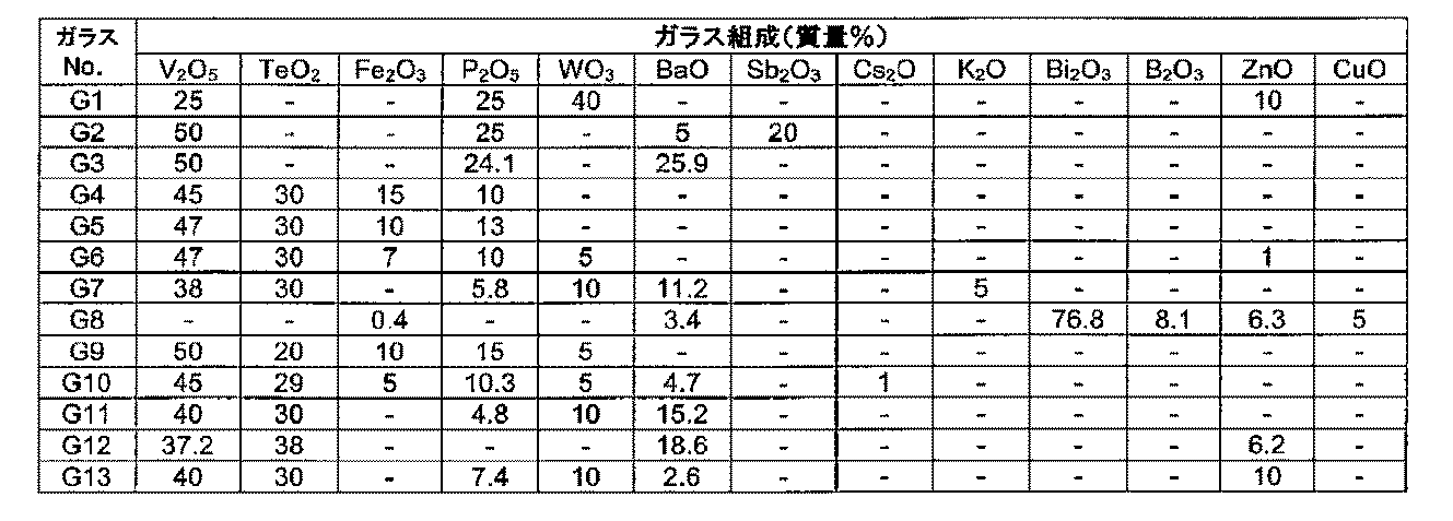
ガラスG1~G13の作製は、以下の手順で行った。まず、原料を表1の組成となるように配合および混合した混合粉末1kgを白金ルツボに入れ、電気炉を用いて5~10℃/分の昇温速度で1000~1200℃の加熱温度まで加熱して2時間保持した。加熱温度の保持中は、均一なガラスとするために攪拌を行った。次に、白金ルツボを電気炉から取り出し、予め100℃に加熱しておいたステンレス板上に熔融したガラスを流し込み、ガラスG1~G13を得た。
次に、接合層の第1接合層および第2接合層を形成するためのガラスペーストを作製した。具体的には、まず、ガラスG1~G13を個別に平均粒径(D50)が約3μmになるまでジェットミルを用いて粉砕してガラスG1~G13の粉末を得た。また、得られたガラスG1~G13の粉末に、フィラー材料として、平均粒径(D50)が約3μmのZr2(WO4)(PO4)2(以下、ZWPと略称する場合がある)、コージェライト(以下、CRDと略称する場合がある)、またはアルミニウム(Al)を所定量加えて混合粉を得た。
次に、ガラスG1~G13の粉末またはフィラー材料を加えた混合粉に、バインダとしてエチルセルロースを加えるとともに、溶剤としてブチルカルビトールアセテートを加えて混錬し、ガラスペーストを作製した。次に、接合層の絶縁基材として、厚さ30μm、熱膨張係数66×10-7/℃の薄板ガラスを用意した。次に、絶縁基材の一方の面にスクリーン印刷によってガラスペーストを塗布して150℃の温度で30分乾燥させたのち、絶縁基材の他方の面にも同様にガラスペーストを塗布して乾燥させた。
その後、脱バインダ処理として、ガラスペーストが塗布された絶縁基材を330℃で30分加熱した。次に、ガラスペーストが塗布された絶縁基材を、接合層の接合温度と同じ温度で仮焼成することで、半導体チップに接合される第1接合層と、基台に接合される第2接合層と、第1接合層と第2接合層との間に配置された絶縁基材とを有する実施例および比較例の接合層を得た。得られた各接合層の厚さは、概ね90μm程度であった。
以下の表2に、実施例E1~E18の接合層の各々の第1接合層および第2接合層について、含有するガラスの種類とその含有量[体積%]、含有するフィラー材料の種類とその含有量[体積%]、熱膨張係数[10-7/℃]、および軟化点[℃]を示す。なお、表2において、ガラスの種類は、表1に示すガラスNo.で示している。
また、以下の表3に、比較例C1~C11の接合層の各々の第1接合層および第2接合層について、含有するガラスの種類とその含有量[体積%]、含有するフィラー材料の種類とその含有量[体積%]、熱膨張係数[10-7/℃]、および軟化点[℃]を示す。なお、表3において、ガラスの種類は、表1に示すガラスNo.で示している。
なお、表2および表3に示す各々の接合層の第1接合層および第2接合層の熱膨張係数の測定は、以下のように行った。まず、バインダおよび溶剤を含まないガラス粉末またはガラス粉末とフィラー材料の混合粉末を一軸加圧成型したのち、電気炉にて緻密に焼き固め、それを切断することにより試験片を得た。試験片の寸法は、4mm×4mm×15mmとした。その試験片を用い、押し棒式熱機械分析装置を用いて50~250℃の範囲の熱膨張係数を測定した。
また、表2および表3に示す各々の接合層の第1接合層および第2接合層の軟化点は、以下のように求めた。まず、上記のガラス粉末または混合粉末を5℃/分の昇温速度で示差熱分析(DTA)を行った。標準サンプルとして、アルミナ粉末を用いた。得られたDTAカーブにおいて、第二吸熱ピーク温度を軟化点Tsとした。
次に、物理量測定装置に用いる半導体チップとして、接合面にメタライズ処理が施されてAl膜が形成された半導体チップ(4mm×4mm、37×10-7/℃)を用意した。また、接合層を介して半導体チップを接合する基台として、ステンレス(SUS630)製のダイアフラム(φ12mm、熱膨張係数:113×10-7/℃)を用意した。
そして、実施例E1~E18および比較例C1~C11の接合層を用い、前述の実施形態で説明した第1配置工程および第2配置工程を行って、各接合層の第1接合層を半導体チップの接合面に対向させ、各接合層の第2接合層を基台の接合面に対向させ、半導体チップと基台との間に接合層を配置した。次に、各接合層を第1接合層の軟化点以上の温度接合温度に加熱し、接合層を介して半導体チップを基台に接合した。
実施例E1~E18の接合層の接合温度、ならびに、接着可否、信頼性、およびチップ動作の評価結果を以下の表4に示す。また、比較例C1~C11の接合層の接合温度、ならびに、接着可否、信頼性、およびチップ動作の評価結果を以下の表5に示す。
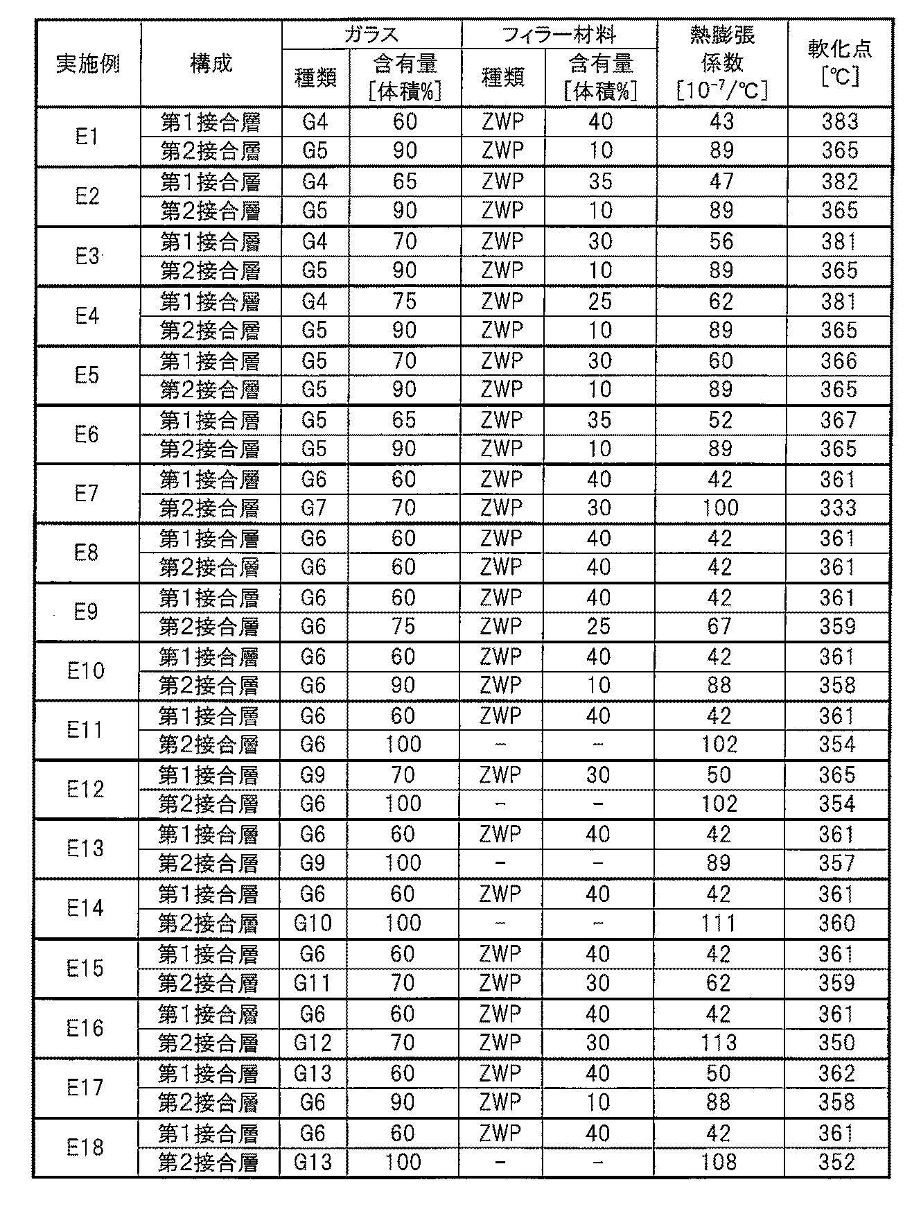
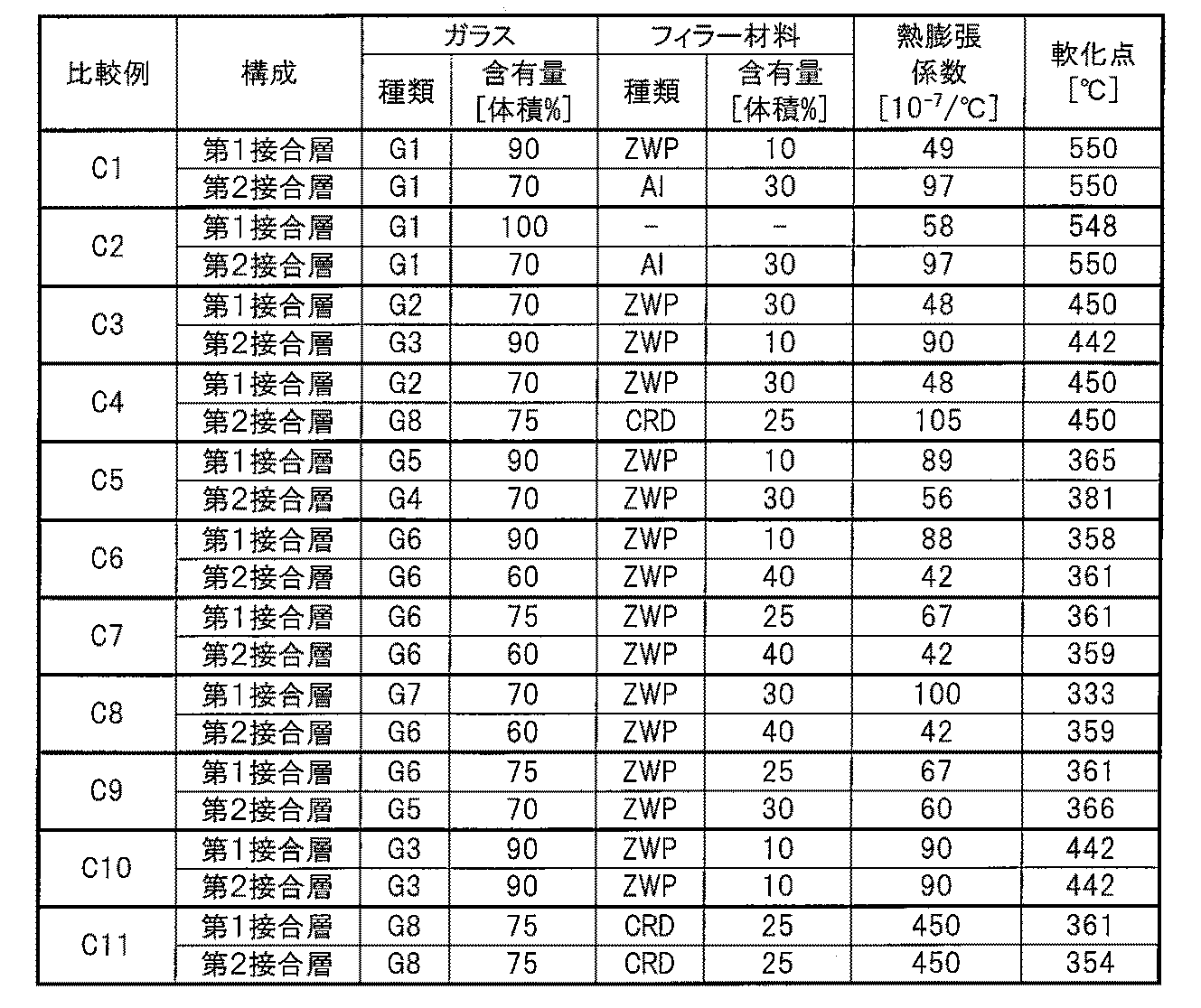
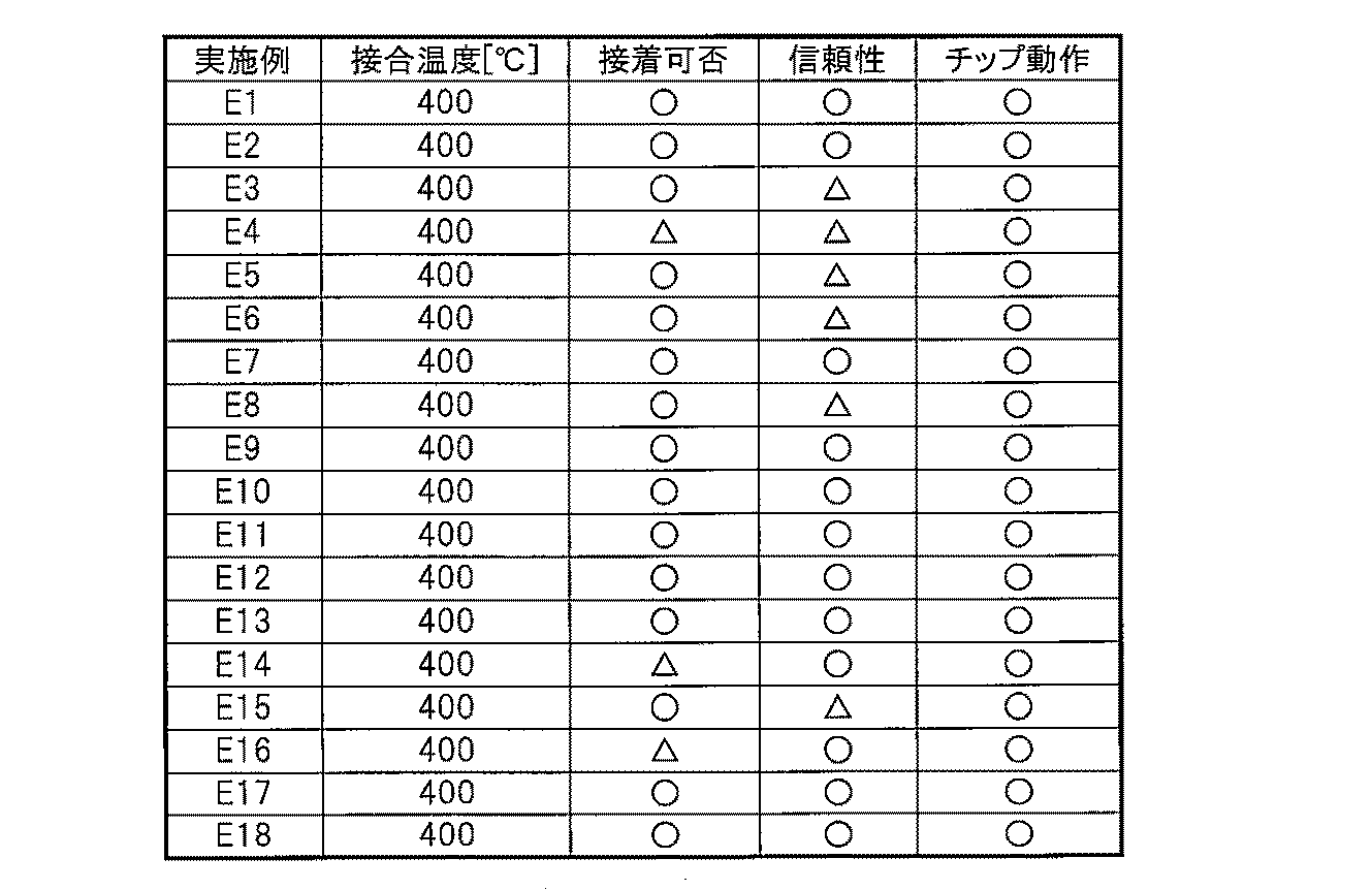
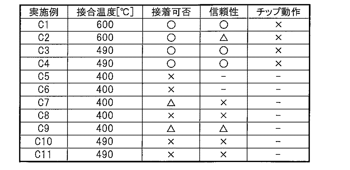
表4および表5に示す接着可否は、複数のサンプルすべてで接合体を介して半導体チップを基台に接合できたものを良(○)と評価した。また、複数のサンプルのうち接合体を介して半導体チップを基台に接合できないものがあったが、問題のないサンプルを多く含むものを可(△)、半導体チップの割れや剥離が生じて半導体チップを基台に接合できなかったものを不可(×)と評価した。
表4および表5に示す信頼性は、接合層を介して接合された半導体チップと基台に対し、-40℃~150℃の温度サイクル試験およびせん断強度試験を行うことによって評価した。その結果、すべてのサンプルに問題が生じなかったものを良(○)と評価した。また、サンプルによっては半導体チップの割れや剥離が生じたり接合強度のばらつきが大きかったりするが、問題のないサンプルを多く含むものを可(△)と評価し、多くのサンプルで半導体チップの割れや剥離が生じるものや接合強度が10Mpa以下となるものは不可(×)と評価した。
表4および表5に示すチップ動作の評価は、基台としてのダイアフラムに各接合層を介して接合された半導体チップを用いて、図1に示される前述の実施形態の物理量測定装置を製作し、半導体チップである歪検出素子の動作を評価することによって行った。その結果、物理量測定装置の動作不良が1%未満の場合には良(○)、10%未満の場合には可(△)、50%以上の場合には不可(×)と評価した。
以上の結果から、第1接合層の熱膨張係数が第2接合層の熱膨張係数以下であり、第1接合層の軟化点が半導体チップの耐熱温度(たとえば430℃)以下であり、第2接合層の軟化点が第1接合層の軟化点以下である実施例E1~E18の接合層を用いた物理量測定装置において、比較例C1~C11と比較して、基台と半導体チップの接合信頼性および半導体チップの動作の信頼性を向上させることができた。
このとき、第1接合層の熱膨張係数としては、42×10-7/℃以上かつ62×10-7/℃以下が良好であり、第2接合層の熱膨張係数としては、42×10-7/℃以上113×10-7/℃以下が良好であった。特に、第1接合層の熱膨張係数が42×10-7/℃以上かつ50×10-7/℃以下で、かつ第2接合層の熱膨張係数が67×10-7/℃以上かつ102×10-7/℃以下の場合に、半導体チップと基台との接合状態および接合信頼性がともに優れた物理量測定装置が得られた。
この優れた結果が得られた実施例では、熱膨張係数αの関係は、歪検出素子の熱膨張係数をα1、上面の接合層の熱膨張係数をα2、絶縁基材の熱膨張係数をα3、下面の接合層の熱膨張係数をα4、ダイアフラムの熱膨張係数をα5としたときに、α1<α2<α3<α4<α5の関係を満たしていた。
また、接合層のフィラー含有量としては、接合材の上面で30~40体積%で、下面が0~40体積%のときに良好な結果が得られた。特に、第1接合層のフィラー材料の含有量が第2接合層のフィラー材料の含有量よりも多い場合に良好な結果が得られた。
また、ガラス組成としては、第1接合層に含まれるガラスの組成は、V2O5が40~50重量%、TeO2が20~30重量%、P2O5が5.8~15重量%、Fe2O3が0~15重量%、WO3が0~10重量%、ZnOが0~10重量%の範囲であり、第2接合層に含まれるガラスの組成は、V2O5が37.2~50重量%、TeO2が20~30重量%、P2O5が0~15重量%、Fe2O3が0~15重量%、WO3が0~10重量%、BaOが0~26重量%、ZnOが0~10重量%の範囲であった。また、その他の成分としてK2OやCs2Oのアルカリ金属酸化物を0~5重量%で含んでいた
。
。
さらに、第2接合層の軟化点が第1接合層の軟化点よりも7℃以上低い場合には、接合層の反りが小さかった。これはガラスの固着温度によるものと考えられるが、接合層の取り扱いの観点からはより好ましいことが判明した。
次に、前述の実施例E1~E18と同様に実施例E19~E21の接合層を作製して、接合層の接合温度による半導体チップへの影響を検討した。なお、実施例E21の接合層では、第2接合層の材料として、市販の鉛系ガラスペーストAGC製、430℃接合用、熱膨張係数72×10-7/℃)を用いた。各接合層の第1接合層および第2接合層の構成を、以下の表6に示す。
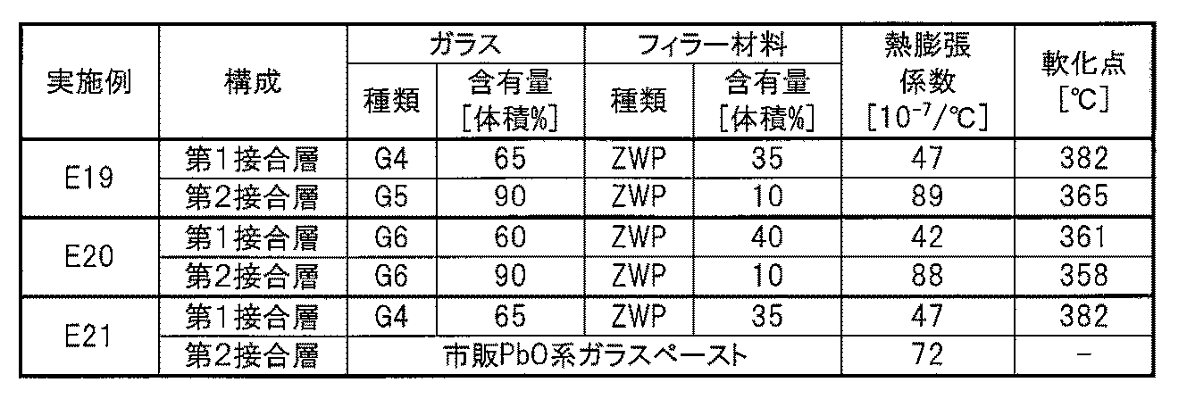
表6に示す各接合層を用いて、半導体チップを基台に接合するときの接合温度を、430℃にした物理量測定装置と、450℃にした物理量測定装置とを作製し、接合層の接合温度による半導体チップへの影響を検証した。結果を表7に示す。
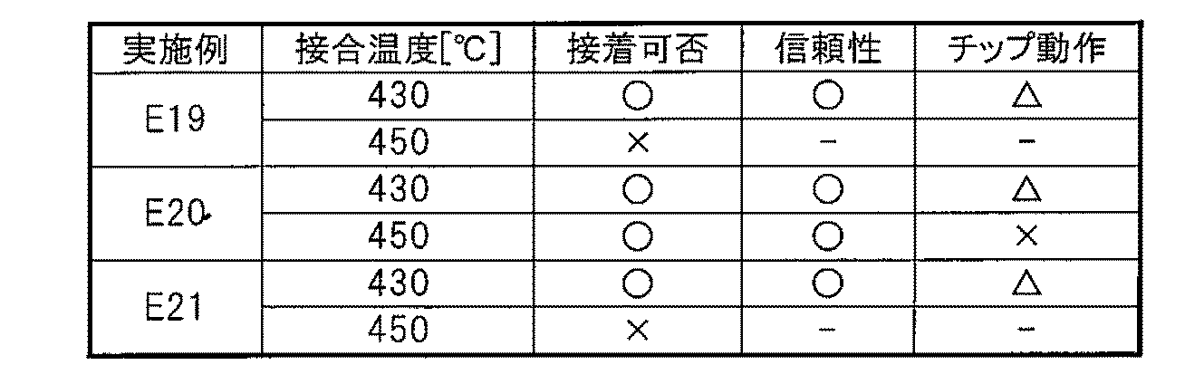
表7に示す各接合層の接着可否、信頼性、およびチップ動作の評価は、表4及び表5に示す各接合層と同様に行った。以上の結果から、接合層の接合温度が半導体チップの耐熱温度(たとえば430℃)以下であれば、接合状態および接合信頼性は良好(○)であり、チップ動作も可(△)であるのに対し、接合層の接合温度が半導体チップの耐熱温度を超えると、接合に不具合が生じたり、半導体チップの動作に異常が見られたりした。したがって、接合層の接合温度は、半導体チップの耐熱温度以下であることが好ましい。なお、接合層の接合温度は、接合層の第1接合層の軟化点以上の温度または第1接合層の軟化点よりも高い温度である。
次に、接合層の絶縁基材による影響を検証するために、絶縁基材の構成以外は実施例E10と同様に実施例E22~E33の接合層を作製した。そして、作製した各接合層を用いて、物理量測定装置を作製した。
また、実施例E10と同様の第1接合層および第2接合層を有し、絶縁基材を有しない比較例C12の接合層を作製した。具体的には、まず、第2接合層を形成するためのガラスペーストを基台であるダイアフラム上に塗布し、乾燥させて仮焼成を行った。その後、第1接合層を形成するためのガラスペーストを仮焼成した第2接合層の上に塗布し、乾燥させて仮焼成を行った。その後、仮焼成した第1接合層の上に半導体チップを配置して400℃で加熱した。これにより、比較例C12の接合層を介して半導体チップを基台に接合し、物理量測定装置を作製した。
その後、実施例E22~E33および比較例C12の接合層を前述の実施例E1からE21と同様に評価した。実施例E22~E33および比較例C12の接合層の絶縁基材の構成、接合温度、ならびに接着可否、信頼性、およびチップ動作の評価結果を以下の表8に示す。
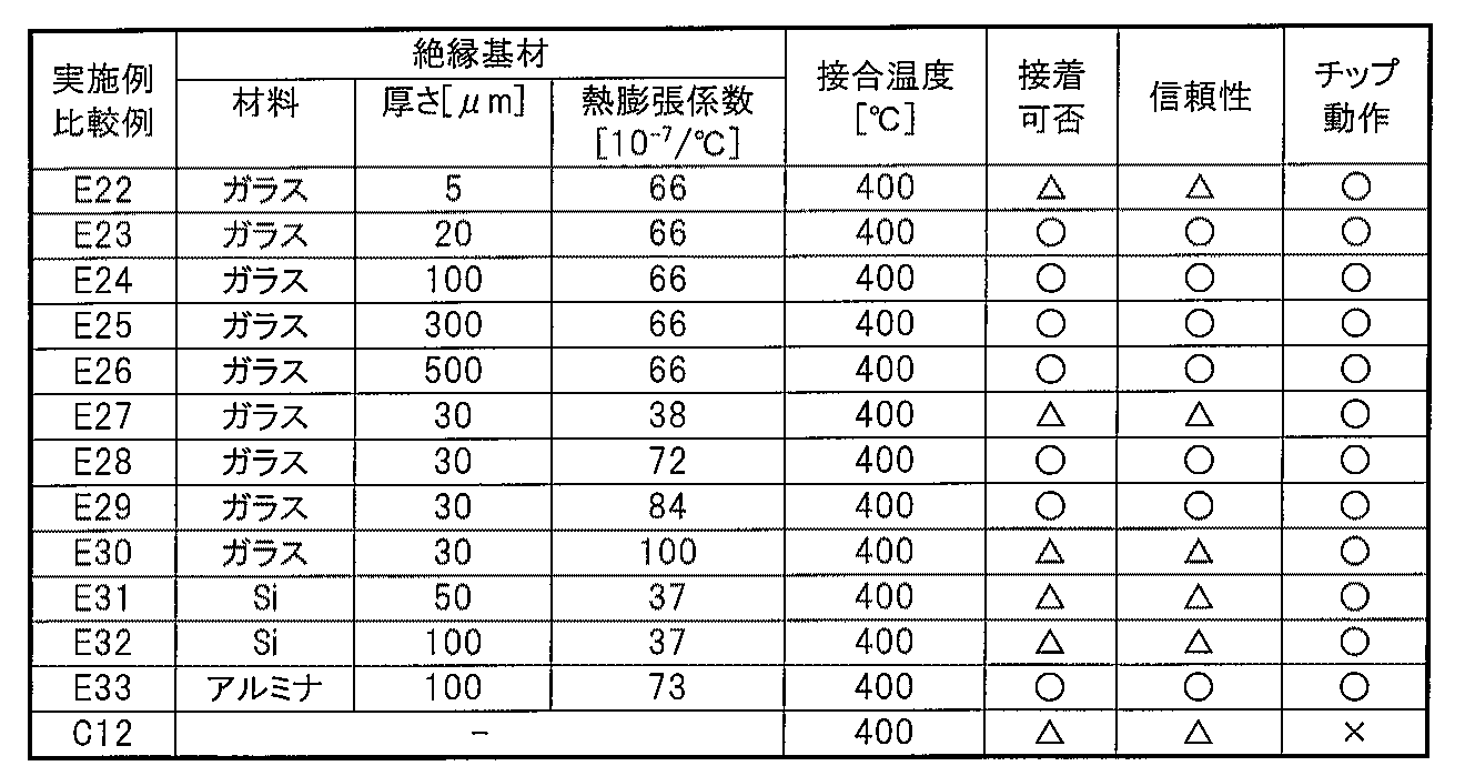
表8において、絶縁材基材の材料であるガラスとしては、SiO2を主成分としたSiO2系ガラスを用いた。また、絶縁材基材の材料であるSiとしては、ドーピングされていない純Siを用いた。表8に示すように、絶縁基材のない比較例C12の接合層を用いた物理量測定装置において、半導体チップの動作に異常が見られたが、絶縁基材を有する実施例E22~E33の接合層を用いた物理量測定装置では、良好にチップが動作することを確認できた。
また、絶縁基材としては、SiO2を主成分としたガラスの他、Siやアルミナなどの一般的な高抵抗の材料であれば使用することができることが確認された。絶縁基材の線熱膨張係数としては、38×10-7/℃以上かつ100×10-7/℃以下まで幅広く使用できることが判明したが、第1および第2接合層との線熱膨張係数の関係から、特に好ましいのは66×10-7/℃以上かつ84×10-7/℃以下の範囲であることが分かった。また、絶縁基材の厚さも5μmから500μm程度まで幅広く使用できるが、特に好ましいのは、信頼性の観点から20μm以上であることが分かった。ただし、絶縁基材の厚さが厚くなると物理量測定装置としての出力が小さくなってしまうことから、特に好ましい絶縁基材の厚さは20μm以上かつ100μm以下である。
最後に、基台の接合層が接合される面に形成された金属膜の効果について検証した。具体的には、基台としてステンレス(SUS630)製のダイアフラムを用い、接合層が接合される基台の接合面に、NiメッキとAlスパッタの前処理を行って金属膜を形成した。そして、実施例E1からE18の接合層を用いて物理量測定装置を作製した。その結果、実施例E1からE18の接合層のいずれの場合にもせん断の接合強度が向上することがわかった。そのため、基台の接合面に前処理を行って、Al、Ni、Ti、Moからなる群から選択される少なくとも1種以上を含む金属膜を形成することが望ましい。
10 金属筐体(基台)
20 接合層
21 第1接合層
22 第2接合層
23 絶縁基材
30 歪検出素子(半導体チップ)
100 物理量測定素子
200 物理量測定装置
S21 第1配置工程
S31 第1接合工程
S22 第2配置工程
S32 第2接合工程
20 接合層
21 第1接合層
22 第2接合層
23 絶縁基材
30 歪検出素子(半導体チップ)
100 物理量測定素子
200 物理量測定装置
S21 第1配置工程
S31 第1接合工程
S22 第2配置工程
S32 第2接合工程
Claims (12)
- 基台と、該基台に作用する応力に基づいて物理量を測定する半導体チップと、該半導体チップを前記基台に接合する接合層とを備える物理量測定装置であって、
前記接合層は、前記半導体チップに接合される第1接合層と、前記基台に接合される第2接合層と、前記第1接合層と前記第2接合層との間に配置された絶縁基材と、を有し、
前記第1接合層および前記第2接合層は、ガラスを含み、
前記第1接合層の熱膨張係数は、前記第2接合層の熱膨張係数以下であり、
前記第1接合層の軟化点は、前記半導体チップの耐熱温度以下であり、
前記第2接合層の軟化点は、前記第1接合層の軟化点以下であることを特徴とする物理量測定装置。 - 前記ガラスは、バナジウムを含むことを特徴とする請求項1に記載の物理量測定装置。
- 前記第1接合層および前記第2接合層は、前記ガラスよりも熱膨張係数が低いフィラー材料を含み、
前記第1接合層の前記フィラー材料の含有率は、前記第2接合層の前記フィラー材料の含有率よりも高いことを特徴とする請求項1に記載の物理量測定装置。 - 前記第1接合層の前記フィラー材料の含有率は、30体積%以上かつ40体積%以下であることを特徴とする請求項3に記載の物理量測定装置。
- 前記第1接合層に含まれる前記ガラスは、V2O5を40~50重量%、TeO2を20~30重量%、P2O5を5.8~15重量%、Fe2O3を0~15重量%、WO3を0~10重量%、ZnOを0~10重量%含み、
前記第2接合層に含まれる前記ガラスは、V2O5を37.2~50重量%、TeO2を20~30重量%、P2O5を0~15重量%、Fe2O3を0~15重量%、WO3を0~10重量%、BaOを0~26重量%、ZnOを0~10重量%、アルカリ金属酸化物を0~5重量%含むことを特徴とする請求項2に記載の物理量測定装置。 - 前記絶縁基材の熱膨張係数は、38×10-7/℃以上かつ100×10-7/℃以下であることを特徴とする請求項1に記載の物理量測定装置。
- 前記絶縁基材の素材は、ガラス、シリコン、またはアルミナであることを特徴とする請求項1に記載の物理量測定装置。
- 前記絶縁基材の厚さは、5μm以上かつ500μm以下であることを特徴とする請求項1に記載の物理量測定装置。
- 前記基台および前記半導体チップは、前記接合層が接合される面に、Al、Ni、Ti、Moからなる群から選択される少なくとも1種以上を含む金属膜を有することを特徴とする請求項1に記載の物理量測定装置。
- 基台と、該基台に作用する応力に基づいて物理量を測定する半導体チップと、該半導体チップを前記基台に接合する接合層とを備える物理量測定装置の製造方法であって、
ガラスを含む第1接合層および第2接合層と、前記第1接合層と前記第2接合層との間に配置された絶縁基材とを備え、前記第1接合層の熱膨張係数が前記第2接合層の熱膨張係数以下であり、前記第1接合層の軟化点が前記半導体チップの耐熱温度以下であり、前記第2接合層の軟化点が前記第1接合層の軟化点以下である前記接合層を用い、前記半導体チップと前記接合層の前記第1接合層とを対向させて配置する第1配置工程と、
前記接合層を前記第1接合層の軟化点以上かつ前記半導体チップの耐熱温度以下の温度に加熱して、前記第1接合層を介して前記半導体チップと前記接合層とを接合する第1接合工程と、
前記基台と前記接合層の前記第2接合層とを対向させて配置する第2配置工程と、
前記接合層を前記第2接合層の軟化点以上かつ前記半導体チップの耐熱温度以下の温度に加熱して、前記第2接合層を介して前記基台と前記接合層とを接合する第2接合工程と、を有することを特徴とする物理量測定装置の製造方法。 - 前記第1配置工程および前記第2配置工程を行って前記半導体チップと前記基台との間に前記接合層を配置した後に、前記接合層を前記第1接合層の軟化点以上かつ前記半導体チップの耐熱温度以下の温度に加熱して前記第1接合工程および前記第2接合工程を一括して行うことを特徴とする請求項10に記載の物理量測定装置の製造方法。
- 基台に作用する応力に基づいて物理量を測定する半導体チップと、該半導体チップを前記基台に接合する接合層と、を備える物理量測定素子であって、
前記接合層は、前記半導体チップに接合される第1接合層と、前記基台に接合される第2接合層と、前記第1接合層と前記第2接合層との間に配置された絶縁基材と、を有し、
前記第1接合層および前記第2接合層は、ガラスを含み、
前記第1接合層の熱膨張係数は、前記第2接合層の熱膨張係数以下であり、
前記第1接合層の軟化点は、前記半導体チップの耐熱温度以下であり、
前記第2接合層の軟化点は、前記第1接合層の軟化点以下であることを特徴とする物理量測定素子。
Priority Applications (3)
| Application Number | Priority Date | Filing Date | Title |
|---|---|---|---|
| CN201780022928.1A CN109154531B (zh) | 2016-05-27 | 2017-04-13 | 物理量测定装置及其制造方法、以及物理量测定元件 |
| DE112017001287.2T DE112017001287B4 (de) | 2016-05-27 | 2017-04-13 | Messvorrichtung für eine physikalische Größe, Verfahren zu ihrer Herstellung und Messelement für eine physikalische Größe |
| US16/094,001 US10788385B2 (en) | 2016-05-27 | 2017-04-13 | Physical quantity measurement device, method for manufacturing same, and physical quantity measurement element |
Applications Claiming Priority (2)
| Application Number | Priority Date | Filing Date | Title |
|---|---|---|---|
| JP2016-106378 | 2016-05-27 | ||
| JP2016106378A JP6486866B2 (ja) | 2016-05-27 | 2016-05-27 | 物理量測定装置およびその製造方法ならびに物理量測定素子 |
Publications (1)
| Publication Number | Publication Date |
|---|---|
| WO2017203878A1 true WO2017203878A1 (ja) | 2017-11-30 |
Family
ID=60411970
Family Applications (1)
| Application Number | Title | Priority Date | Filing Date |
|---|---|---|---|
| PCT/JP2017/015069 Ceased WO2017203878A1 (ja) | 2016-05-27 | 2017-04-13 | 物理量測定装置およびその製造方法ならびに物理量測定素子 |
Country Status (5)
| Country | Link |
|---|---|
| US (1) | US10788385B2 (ja) |
| JP (1) | JP6486866B2 (ja) |
| CN (1) | CN109154531B (ja) |
| DE (1) | DE112017001287B4 (ja) |
| WO (1) | WO2017203878A1 (ja) |
Families Citing this family (3)
| Publication number | Priority date | Publication date | Assignee | Title |
|---|---|---|---|---|
| DE102018221984A1 (de) * | 2018-12-17 | 2020-06-18 | Robert Bosch Gmbh | Verfahren zur Herstellung einer Sensoranforderung zur Bestimmung mindestens eines Drucks eines fluiden Mediums |
| CN112762993B (zh) * | 2020-12-29 | 2021-10-08 | 深圳市韦德勋光电科技有限公司 | 一种用于lcd逻辑板基板原材的探测装置及使用方法 |
| KR20250059409A (ko) | 2022-09-07 | 2025-05-02 | 구와나 메탈스, 엘티디. | 반도체 칩을 유리 접합하는 방법, 압력 센서의 제조 방법 및 접합 장치 |
Citations (1)
| Publication number | Priority date | Publication date | Assignee | Title |
|---|---|---|---|---|
| WO2015040737A1 (ja) * | 2013-09-20 | 2015-03-26 | 株式会社日立製作所 | 半導体素子の接合構造 |
Family Cites Families (12)
| Publication number | Priority date | Publication date | Assignee | Title |
|---|---|---|---|---|
| DE10036284A1 (de) * | 2000-07-26 | 2002-02-07 | Bosch Gmbh Robert | Herstellungsverfahren für ein Sensorbauelement, insbesondere Dünnschicht-Hochdrucksensor und Sensorbauelement |
| US7626275B2 (en) * | 2005-12-16 | 2009-12-01 | Mitsubishi Electric Corporation | Semiconductor device |
| DE102006047395A1 (de) * | 2006-10-06 | 2008-04-10 | Robert Bosch Gmbh | Verfahren zur Herstellung eines Sensorbauelements und Sensorbauelement |
| JP5746997B2 (ja) | 2011-06-07 | 2015-07-08 | 富士フイルム株式会社 | 電子内視鏡装置の製造方法 |
| JP5726698B2 (ja) | 2011-07-04 | 2015-06-03 | 株式会社日立製作所 | ガラス組成物、それを含むガラスフリット、それを含むガラスペースト、およびそれを利用した電気電子部品 |
| JP2013036935A (ja) | 2011-08-10 | 2013-02-21 | Nippon Soken Inc | 圧力センサおよびその製造方法 |
| JP6036152B2 (ja) | 2012-10-18 | 2016-11-30 | 日立化成株式会社 | 電子部品及びその製法、封止材料ペースト、フィラー粒子 |
| WO2015098324A1 (ja) | 2013-12-25 | 2015-07-02 | 日立オートモティブシステムズ株式会社 | 圧力測定装置 |
| FI126999B (en) * | 2014-01-17 | 2017-09-15 | Murata Manufacturing Co | Improved pressure sensor |
| WO2017006840A1 (ja) | 2015-07-07 | 2017-01-12 | 日立オートモティブシステムズ株式会社 | 半導体装置、力学量測定装置および半導体装置の製造方法 |
| JP6457109B2 (ja) * | 2015-10-28 | 2019-01-23 | 日立オートモティブシステムズ株式会社 | 圧力検出装置 |
| JP6607816B2 (ja) * | 2016-03-30 | 2019-11-20 | 日立オートモティブシステムズ株式会社 | 圧力測定装置 |
-
2016
- 2016-05-27 JP JP2016106378A patent/JP6486866B2/ja active Active
-
2017
- 2017-04-13 WO PCT/JP2017/015069 patent/WO2017203878A1/ja not_active Ceased
- 2017-04-13 US US16/094,001 patent/US10788385B2/en active Active
- 2017-04-13 CN CN201780022928.1A patent/CN109154531B/zh active Active
- 2017-04-13 DE DE112017001287.2T patent/DE112017001287B4/de active Active
Patent Citations (1)
| Publication number | Priority date | Publication date | Assignee | Title |
|---|---|---|---|---|
| WO2015040737A1 (ja) * | 2013-09-20 | 2015-03-26 | 株式会社日立製作所 | 半導体素子の接合構造 |
Also Published As
| Publication number | Publication date |
|---|---|
| DE112017001287B4 (de) | 2024-09-26 |
| CN109154531B (zh) | 2020-09-29 |
| JP2017211338A (ja) | 2017-11-30 |
| CN109154531A (zh) | 2019-01-04 |
| US10788385B2 (en) | 2020-09-29 |
| JP6486866B2 (ja) | 2019-03-20 |
| DE112017001287T5 (de) | 2018-12-06 |
| US20190128758A1 (en) | 2019-05-02 |
Similar Documents
| Publication | Publication Date | Title |
|---|---|---|
| US9714869B2 (en) | Temperature sensor including thermosensitive element | |
| JP6154488B2 (ja) | 圧力測定装置 | |
| JP6486866B2 (ja) | 物理量測定装置およびその製造方法ならびに物理量測定素子 | |
| EP2362938B1 (en) | Sensor element and process for assembling a sensor element | |
| JPH0749277A (ja) | 圧力センサ及び圧力センサの製法 | |
| US20130321002A1 (en) | Sensor assemblies | |
| US8915142B2 (en) | Ceramic component having at least one electrical feedthrough, method for its manufacture and pressure sensor with such a component | |
| US10442724B2 (en) | Joining material and joined body using same | |
| JP6297914B2 (ja) | 感温素子および温度センサ | |
| US20210190617A1 (en) | Sensor element and method for manufacturing same, and sensor device | |
| CN107743578B (zh) | 具有活性钎焊的压力传感器 | |
| JP6404726B2 (ja) | 感温素子及び温度センサ | |
| JP6726802B2 (ja) | 物理量測定装置およびその製造方法ならびに物理量測定素子 | |
| JP6607816B2 (ja) | 圧力測定装置 | |
| JP6404725B2 (ja) | 感温素子及び温度センサ | |
| JP2011038926A (ja) | 温度センサ | |
| JP6909354B2 (ja) | 物理量測定装置 | |
| JP2013189332A (ja) | 焼結体、焼結体の製造方法および温度センサ | |
| JP6430910B2 (ja) | 感温素子および温度センサ | |
| JPH09255360A (ja) | 結晶性ガラス組成物 | |
| JPH05296865A (ja) | 圧力検出器 |
Legal Events
| Date | Code | Title | Description |
|---|---|---|---|
| 121 | Ep: the epo has been informed by wipo that ep was designated in this application |
Ref document number: 17802477 Country of ref document: EP Kind code of ref document: A1 |
|
| 122 | Ep: pct application non-entry in european phase |
Ref document number: 17802477 Country of ref document: EP Kind code of ref document: A1 |