WO2017191758A1 - 距離センサおよび距離センサの駆動方法 - Google Patents
距離センサおよび距離センサの駆動方法 Download PDFInfo
- Publication number
- WO2017191758A1 WO2017191758A1 PCT/JP2017/015746 JP2017015746W WO2017191758A1 WO 2017191758 A1 WO2017191758 A1 WO 2017191758A1 JP 2017015746 W JP2017015746 W JP 2017015746W WO 2017191758 A1 WO2017191758 A1 WO 2017191758A1
- Authority
- WO
- WIPO (PCT)
- Prior art keywords
- region
- charge
- potential
- transfer
- light
- Prior art date
- Legal status (The legal status is an assumption and is not a legal conclusion. Google has not performed a legal analysis and makes no representation as to the accuracy of the status listed.)
- Ceased
Links
Images








Classifications
-
- G—PHYSICS
- G01—MEASURING; TESTING
- G01S—RADIO DIRECTION-FINDING; RADIO NAVIGATION; DETERMINING DISTANCE OR VELOCITY BY USE OF RADIO WAVES; LOCATING OR PRESENCE-DETECTING BY USE OF THE REFLECTION OR RERADIATION OF RADIO WAVES; ANALOGOUS ARRANGEMENTS USING OTHER WAVES
- G01S7/00—Details of systems according to groups G01S13/00, G01S15/00, G01S17/00
- G01S7/48—Details of systems according to groups G01S13/00, G01S15/00, G01S17/00 of systems according to group G01S17/00
- G01S7/483—Details of pulse systems
- G01S7/486—Receivers
- G01S7/4861—Circuits for detection, sampling, integration or read-out
- G01S7/4863—Detector arrays, e.g. charge-transfer gates
-
- G—PHYSICS
- G01—MEASURING; TESTING
- G01C—MEASURING DISTANCES, LEVELS OR BEARINGS; SURVEYING; NAVIGATION; GYROSCOPIC INSTRUMENTS; PHOTOGRAMMETRY OR VIDEOGRAMMETRY
- G01C3/00—Measuring distances in line of sight; Optical rangefinders
- G01C3/02—Details
- G01C3/06—Use of electric means to obtain final indication
-
- G—PHYSICS
- G01—MEASURING; TESTING
- G01S—RADIO DIRECTION-FINDING; RADIO NAVIGATION; DETERMINING DISTANCE OR VELOCITY BY USE OF RADIO WAVES; LOCATING OR PRESENCE-DETECTING BY USE OF THE REFLECTION OR RERADIATION OF RADIO WAVES; ANALOGOUS ARRANGEMENTS USING OTHER WAVES
- G01S17/00—Systems using the reflection or reradiation of electromagnetic waves other than radio waves, e.g. lidar systems
- G01S17/02—Systems using the reflection of electromagnetic waves other than radio waves
- G01S17/06—Systems determining position data of a target
- G01S17/08—Systems determining position data of a target for measuring distance only
- G01S17/10—Systems determining position data of a target for measuring distance only using transmission of interrupted, pulse-modulated waves
-
- G—PHYSICS
- G01—MEASURING; TESTING
- G01S—RADIO DIRECTION-FINDING; RADIO NAVIGATION; DETERMINING DISTANCE OR VELOCITY BY USE OF RADIO WAVES; LOCATING OR PRESENCE-DETECTING BY USE OF THE REFLECTION OR RERADIATION OF RADIO WAVES; ANALOGOUS ARRANGEMENTS USING OTHER WAVES
- G01S17/00—Systems using the reflection or reradiation of electromagnetic waves other than radio waves, e.g. lidar systems
- G01S17/88—Lidar systems specially adapted for specific applications
- G01S17/89—Lidar systems specially adapted for specific applications for mapping or imaging
-
- G—PHYSICS
- G01—MEASURING; TESTING
- G01S—RADIO DIRECTION-FINDING; RADIO NAVIGATION; DETERMINING DISTANCE OR VELOCITY BY USE OF RADIO WAVES; LOCATING OR PRESENCE-DETECTING BY USE OF THE REFLECTION OR RERADIATION OF RADIO WAVES; ANALOGOUS ARRANGEMENTS USING OTHER WAVES
- G01S17/00—Systems using the reflection or reradiation of electromagnetic waves other than radio waves, e.g. lidar systems
- G01S17/88—Lidar systems specially adapted for specific applications
- G01S17/89—Lidar systems specially adapted for specific applications for mapping or imaging
- G01S17/894—Three-dimensional [3D] imaging with simultaneous measurement of time-of-flight at a two-dimensional [2D] array of receiver pixels, e.g. time-of-flight cameras or flash lidar
-
- G—PHYSICS
- G01—MEASURING; TESTING
- G01S—RADIO DIRECTION-FINDING; RADIO NAVIGATION; DETERMINING DISTANCE OR VELOCITY BY USE OF RADIO WAVES; LOCATING OR PRESENCE-DETECTING BY USE OF THE REFLECTION OR RERADIATION OF RADIO WAVES; ANALOGOUS ARRANGEMENTS USING OTHER WAVES
- G01S7/00—Details of systems according to groups G01S13/00, G01S15/00, G01S17/00
- G01S7/48—Details of systems according to groups G01S13/00, G01S15/00, G01S17/00 of systems according to group G01S17/00
- G01S7/483—Details of pulse systems
- G01S7/486—Receivers
-
- H—ELECTRICITY
- H04—ELECTRIC COMMUNICATION TECHNIQUE
- H04N—PICTORIAL COMMUNICATION, e.g. TELEVISION
- H04N25/00—Circuitry of solid-state image sensors [SSIS]; Control thereof
- H04N25/60—Noise processing, e.g. detecting, correcting, reducing or removing noise
-
- H—ELECTRICITY
- H04—ELECTRIC COMMUNICATION TECHNIQUE
- H04N—PICTORIAL COMMUNICATION, e.g. TELEVISION
- H04N25/00—Circuitry of solid-state image sensors [SSIS]; Control thereof
- H04N25/70—SSIS architectures; Circuits associated therewith
- H04N25/76—Addressed sensors, e.g. MOS or CMOS sensors
-
- H—ELECTRICITY
- H10—SEMICONDUCTOR DEVICES; ELECTRIC SOLID-STATE DEVICES NOT OTHERWISE PROVIDED FOR
- H10F—INORGANIC SEMICONDUCTOR DEVICES SENSITIVE TO INFRARED RADIATION, LIGHT, ELECTROMAGNETIC RADIATION OF SHORTER WAVELENGTH OR CORPUSCULAR RADIATION
- H10F39/00—Integrated devices, or assemblies of multiple devices, comprising at least one element covered by group H10F30/00, e.g. radiation detectors comprising photodiode arrays
- H10F39/10—Integrated devices
- H10F39/12—Image sensors
-
- H—ELECTRICITY
- H04—ELECTRIC COMMUNICATION TECHNIQUE
- H04N—PICTORIAL COMMUNICATION, e.g. TELEVISION
- H04N25/00—Circuitry of solid-state image sensors [SSIS]; Control thereof
- H04N25/60—Noise processing, e.g. detecting, correcting, reducing or removing noise
- H04N25/63—Noise processing, e.g. detecting, correcting, reducing or removing noise applied to dark current
- H04N25/633—Noise processing, e.g. detecting, correcting, reducing or removing noise applied to dark current by using optical black pixels
Definitions
- the present invention relates to a distance sensor and a driving method of the distance sensor.
- Patent Document 1 A time-of-flight (TOF) method that measures the distance to an object based on the time difference between the timing at which light is emitted from the light source and the timing at which reflected light from the object arrives is known.
- TOF time-of-flight
- Patent Document 1 describes a distance sensor based on the TOF method.
- the distance sensor described in Patent Document 1 has a charge distribution type configuration, and a charge generated in a first period after irradiation with pulsed light and a second after a first period. Charges generated in the period are accumulated in accumulation nodes coupled to different charge collection regions. Then, the distance to the object is calculated based on the ratio of the amount of charge stored in these storage nodes.
- Non-Patent Document 1 describes a method of irradiating triangular wave light and measuring the distance to the object based on the phase difference between the irradiated light and the reflected light.
- the inventors have found the following problems as a result of examining the above-described conventional technology. That is, in the distance sensor, not only the charge due to reflected light but also the charge due to disturbance light is generally accumulated in the accumulation node. In the distance sensor described in Patent Literature 1, when calculating the distance, the amount of charge corresponding to disturbance light is subtracted from the amount of charge obtained at each storage node. Therefore, there is a problem that both the charge due to reflected light and the charge due to disturbance light are accumulated in each accumulation node, and the accumulation node is likely to be saturated. Note that the method described in Patent Document 1 has an advantage that the intensity of irradiation light (that is, the S / N ratio) with respect to the intensity of disturbance light can be increased because pulsed light is output.
- the intensity of irradiation light that is, the S / N ratio
- Non-Patent Document 1 since the object is irradiated with triangular wave light, in order to capture all the charges generated during one cycle, it is always any one during one cycle. These transfer electrodes must be set to an ON potential (potential that enables charge transfer). In this case, a large amount of charge due to disturbance light is taken in, and each storage node is likely to be saturated. In addition, since the light emission state of the light source is continuous as compared with the case where pulsed light is output, the intensity of the irradiation light is kept low, and the intensity of the irradiation light with respect to the intensity of the disturbance light (ie, the S / N ratio). ) was low.
- the present invention has been made to solve the above-described problems, such as storage nodes electrically coupled to charge collection regions in which charges in the photosensitive region are distributed by driving a plurality of transfer electrodes.
- the distance sensor is a distance sensor that measures the distance to an object by irradiating the object with light and detecting reflected light from the object.
- An irradiation unit, a semiconductor substrate, a first transfer electrode, a second transfer electrode, and a drive unit are provided.
- the light irradiation unit repeatedly irradiates the object with pulsed light.
- the semiconductor substrate has a photosensitive region and first and second charge collection regions.
- the light sensitive region is a region that generates electric charge according to the amount of reflected light.
- Each of the first and second charge collection regions is a region that is arranged at a predetermined distance from the photosensitive region and collects charges from the photosensitive region.
- the first transfer electrode is an electrode that is disposed on a region between the photosensitive region and the first charge collection region and can be set to an on potential or an off potential.
- the on potential is a potential that enables charge transfer from the photosensitive region to the first charge collection region
- the off potential is a potential that stops the charge transfer.
- the second transfer electrode is disposed on a region between the photosensitive region and the second charge collection region, and is a potential that enables charge transfer from the photosensitive region to the second charge collection region, The off potential is a potential for stopping the charge transfer.
- Each of the drive units constitutes an electrode drive pattern for driving the first and second transfer electrodes, and a plurality of frames defined at equally spaced times t 0 , t 1 ,..., T 9.
- the light irradiating unit irradiates light in each of the plurality of frames from time t 1 to time t 3 .
- the driving unit sets the first transfer electrode to the on-potential between times t 0 to t 2 and t 4 to t 6 in the first frame of the plurality of frames, while setting the second transfer electrode to The on potential is set between time t 2 to t 4 and t 6 to t 8 .
- the drive unit sets the first transfer electrode to the on-potential between times t 1 to t 3 and t 5 to t 7 in the second frame different from the first frame, while the second transfer electrode Is set to the ON potential during times t 3 to t 5 and t 7 to t 9 .
- the distance sensor according to the present embodiment is a distance sensor that irradiates an object with pulsed light, and is electrically coupled to a charge collection region to which charges in the photosensitive region are distributed by driving a plurality of transfer electrodes.
- the storage node has a structure for injecting an equal amount of current while obtaining the distance to the object based on the difference information of the charge amount of each storage node. Therefore, saturation caused by disturbance light at each storage node is avoided by injecting an equal amount of current into each storage node, regardless of the distance sensor and the driving method for driving the distance sensor.
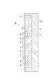
- FIG. 3 is a sectional view taken along line III-III in FIG.
- FIG. 4 is a sectional view taken along line IV-IV in FIG.
- the graph which shows the example of the time change of the intensity
- FIG. 9 is a diagram further showing a chart of a received light pulse waveform of reflected light in the timing chart shown in FIG. 8.
- FIG. 9 is a diagram further showing a chart of a received light pulse waveform of reflected light in the timing chart shown in FIG. 8.
- FIG. 17 is a sectional view taken along line XVII-XVII in FIG.
- a distance sensor is a distance sensor that measures the distance to an object by irradiating the object with light and detecting reflected light from the object.
- a light irradiation part a semiconductor substrate, a 1st transfer electrode, a 2nd transfer electrode, and a drive part are provided.
- the light irradiation unit repeatedly irradiates the object with pulsed light.
- the semiconductor substrate has a photosensitive region and first and second charge collection regions.
- the light sensitive region is a region that generates electric charge according to the amount of reflected light.
- Each of the first and second charge collection regions is a region that is arranged at a predetermined distance from the photosensitive region and collects charges from the photosensitive region.
- the first transfer electrode is an electrode that is disposed on a region between the photosensitive region and the first charge collection region and can be set to an on potential or an off potential.
- the on potential is a potential that enables charge transfer from the photosensitive region to the first charge collection region
- the off potential is a potential that stops the charge transfer.
- the second transfer electrode is disposed on a region between the photosensitive region and the second charge collection region, and is a potential that enables charge transfer from the photosensitive region to the second charge collection region, The off potential is a potential for stopping the charge transfer.
- Each of the drive units constitutes an electrode drive pattern for driving the first and second transfer electrodes, and a plurality of frames defined at equally spaced times t 0 , t 1 ,..., T 9.
- the light irradiating unit irradiates light in each of the plurality of frames from time t 1 to time t 3 .
- the driving unit sets the first transfer electrode to the on-potential between times t 0 to t 2 and t 4 to t 6 in the first frame of the plurality of frames, while setting the second transfer electrode to The on potential is set between time t 2 to t 4 and t 6 to t 8 .
- the drive unit sets the first transfer electrode to the on-potential between times t 1 to t 3 and t 5 to t 7 in the second frame different from the first frame, while the second transfer electrode Is set to the ON potential during times t 3 to t 5 and t 7 to t 9 .
- each of the drive units in the distance sensor constitutes an electrode drive pattern for driving the first and second transfer electrodes, and is equally spaced at time t 0 .
- the first and second transfer electrodes may be driven by sequentially executing a plurality of frames defined by t 1 ,..., t 8 .
- the light irradiator irradiates light in each of the plurality of frames from time t 1 to t 3 .
- the driving unit sets the first transfer electrode to the on potential between time t 0 to t 1 and t 4 to t 5 , while setting the second transfer electrode to time t 2 set between oN potential of ⁇ t 3 and t 6 ⁇ t 7. Further, the driving unit sets the first transfer electrode to the on-potential between times t 1 to t 2 and t 5 to t 6 in the second frame different from the first frame, while the second transfer electrode Is set to the on potential during times t 3 to t 4 and t 7 to t 8 .
- the distance sensor may include a light irradiation unit, a semiconductor substrate, first to fourth transfer electrodes, and a driving unit.
- the light irradiation unit repeatedly irradiates the object with pulsed light.
- the semiconductor substrate has a photosensitive region and first to fourth charge collection regions.
- the light sensitive region generates a charge corresponding to the amount of reflected light.
- Each of the first to fourth charge collection regions is arranged in a state of being separated from the photosensitive region by a predetermined distance, and collects charges from the photosensitive region.
- the first transfer electrode is disposed on a region between the light sensitive region and the first charge collection region
- the second transfer electrode is disposed on a region between the light sensitive region and the second charge collection region.
- the third transfer electrode is disposed on a region between the photosensitive region and the third charge collection region
- the fourth transfer electrode is disposed between the photosensitive region and the fourth charge collection region. It is arranged on the area between.
- Each of the first to fourth transfer electrodes is an electrode that can be set to an on potential that enables charge transfer from the photosensitive region to the corresponding charge collection region or an off potential that stops this charge transfer.
- Each of the drive units constitutes an electrode drive pattern for driving the first to fourth transfer electrodes, and a plurality of frames defined at equally spaced times t 0 , t 1 ,..., T 8. Are sequentially executed to drive the first to fourth transfer electrodes.
- the light irradiating unit irradiates light in each of the plurality of frames from time t 1 to time t 3 .
- the driving unit sets the first transfer electrode to an on potential between times t 0 to t 1 and t 4 to t 5 , and sets the second transfer electrode to times t 1 to t 2 and t
- the on potential is set between 5 and t 6
- the third transfer electrode is set at the on potential between times t 2 and t 3 and t 6 and t 7
- the fourth transfer electrode is set between times t 3 and t 4.
- the distance sensor driving method drives a distance sensor that measures the distance to the object by irradiating the object with light and detecting reflected light from the object.
- the distance sensor to be driven includes a light irradiation unit, a semiconductor substrate, a first transfer electrode, and a second transfer electrode.
- the light irradiation unit repeatedly irradiates the object with pulsed light.
- the semiconductor substrate has a photosensitive region and first and second charge collection regions.
- the light sensitive region is a region that generates electric charge according to the amount of reflected light.
- Each of the first and second charge collection regions is a region that is arranged at a predetermined distance from the photosensitive region and collects charges from the photosensitive region.
- the first transfer electrode is an electrode that is disposed on a region between the photosensitive region and the first charge collection region and can be set to an on potential or an off potential.
- the on potential is a potential that enables charge transfer from the photosensitive region to the first charge collection region
- the off potential is a potential that stops the charge transfer.
- the second transfer electrode is disposed on a region between the photosensitive region and the second charge collection region, and is a potential that enables charge transfer from the photosensitive region to the second charge collection region,
- the off potential is a potential for stopping the charge transfer.
- each of them constitutes an electrode driving pattern for driving the first and second transfer electrodes, and at equally spaced times t 0 , t 1 ,..., T 9 .
- a plurality of defined frames are executed in order. Specifically, in the driving method, light is emitted from the light irradiation unit between times t 1 and t 3 in each of a plurality of frames.
- the first transfer electrode is set to the on-potential between times t 0 to t 2 and t 4 to t 6 , while the second transfer is performed.
- the electrodes are set to the on potential during times t 2 to t 4 and t 6 to t 8 .
- the first transfer electrode is set to the on potential during the times t 1 to t 3 and t 5 to t 7 , while the second frame The transfer electrode is set to the on potential during times t 3 to t 5 and t 7 to t 9 .
- the driving method uses a distance sensor having the above-described structure as a driving target, and each has an electrode driving pattern for driving the first and second transfer electrodes.
- a plurality of frames defined at equidistant times t 0 , t 1 ,..., T 8 may be sequentially executed.
- light is irradiated from the light irradiation unit in each of the plurality of frames during times t 1 to t 3 of each frame.
- the first transfer electrode is set to the on potential during the times t 0 to t 1 and t 4 to t 5 , while the second transfer is performed.
- the electrodes are set to the on potential during times t 2 to t 3 and t 6 to t 7 . Further, in the driving method, in the second frame different from the first frame, the first transfer electrode is set to the on potential during the times t 1 to t 2 and t 5 to t 6 , while the second frame The transfer electrode is set to the on potential during times t 3 to t 4 and t 7 to t 8 .
- a distance sensor to be driven by the driving method may include a light irradiation unit, a semiconductor substrate, and first to fourth transfer electrodes.
- the light irradiation unit repeatedly irradiates the object with pulsed light.
- the semiconductor substrate has a photosensitive region and first to fourth charge collection regions.
- the light sensitive region generates a charge corresponding to the amount of reflected light.
- Each of the first to fourth charge collection regions is arranged in a state of being separated from the photosensitive region by a predetermined distance, and collects charges from the photosensitive region.
- the first transfer electrode is disposed on a region between the light sensitive region and the first charge collection region, and the second transfer electrode is disposed on a region between the light sensitive region and the second charge collection region.
- the third transfer electrode is disposed on a region between the photosensitive region and the third charge collection region, and the fourth transfer electrode is disposed between the photosensitive region and the fourth charge collection region. It is arranged on the area between.
- Each of the first to fourth transfer electrodes is an electrode that can be set to an on potential that enables charge transfer from the photosensitive region to the corresponding charge collection region or an off potential that stops this charge transfer.
- Each of the driving methods for driving the distance sensor having the structure as described above constitutes an electrode driving pattern for driving the first to fourth transfer electrodes, and at equal time t 0 , t 1 ,..., T 8 are sequentially executed.
- the driving method in each of a plurality of frames, light is emitted from the light irradiating unit from time t 1 to t 3 , and the first transfer electrode is time t 0 to t 1 and t 4 to t 5.
- the second transfer electrode is set to the on potential during times t 1 to t 2 and t 5 to t 6
- the third transfer electrode is set to the times t 2 to t 3 and t 6 to t 6 .
- the on potential is set during t 7
- the fourth transfer electrode is set to the on potential between times t 3 to t 4 and t 7 to t 8 .
- the distance can be obtained from the difference in the amount of charge accumulated in each accumulation node, as described in the embodiments described later. Therefore, saturation of each storage node can be avoided by injecting an equal amount of current into each storage node.
- the semiconductor substrate collects electric charges from the photosensitive region arranged in a state of being separated from the photosensitive region by a predetermined distance.
- a fifth charge collection region may be further included.
- the distance sensor includes a fifth transfer electrode disposed on a region between the photosensitive region and the fifth charge collection region. May be further provided.
- the driving unit sets the fifth transfer electrode to the on potential except for a period from when the other transfer electrode is first set to the on potential until the last is set to the off potential. Set.
- the fifth transfer electrode is set to the on potential except for a period from when the other transfer electrode is first set to the on potential until it is finally set to the off potential.
- the fifth and the fifth transfer electrodes are not driven except for the period during which the first and second transfer electrodes are driven. Charges due to disturbance light can be discharged using the transfer electrode. Accordingly, it is possible to further suppress saturation due to disturbance light and to reduce shot noise due to disturbance light, so that resistance to disturbance light and distance measurement accuracy can be further improved.
- each aspect listed in this [Description of Embodiments of the Invention] is applicable to each of all the remaining aspects or to all combinations of these remaining aspects. .
- FIG. 1 is a plan view showing a configuration of a distance sensor 1A according to an embodiment of the present invention.
- the distance sensor 1A measures the distance to the object by irradiating the object with light and detecting the reflected light from the object.
- the distance sensor 1 ⁇ / b> A includes an imaging region 5 formed on the semiconductor substrate 3, a sensor drive circuit 7 (drive unit), and a processing circuit 8.
- the sensor drive circuit 7 drives the imaging area 5.
- the processing circuit 8 processes the output of the imaging area 5.
- the imaging region 5 includes a plurality of pixels P arranged in a one-dimensional or two-dimensional manner on the semiconductor substrate 3.
- FIG. 1 is a plan view showing a configuration of a distance sensor 1A according to an embodiment of the present invention.
- the distance sensor 1A measures the distance to the object by irradiating the object with light and detecting the reflected light from the object.
- the distance sensor 1 ⁇ / b> A includes an imaging region 5 formed on the semiconductor substrate 3, a sensor drive circuit 7
- Each pixel P (m, n) includes a light receiving unit 9 and a current injection circuit 20.
- the imaging region 5 detects reflected light from the object for each pixel P. And the distance for every pixel P of the image of a target object is calculated
- the distance sensor 1A is a charge distribution type distance sensor, and the time from when the light is irradiated until the reflected light arrives depends on the ratio of the amount of charge distributed to two locations in each pixel P. Ask.
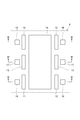
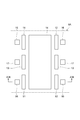
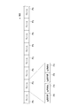
- FIG. 2 is a plan view of the light receiving unit 9 of each pixel P (m, n) of the distance sensor 1A shown in FIG. 3 and 4 are sectional views taken along lines III-III and IV-IV, respectively, of FIG. In FIG. 3, the light source unit 30 is also shown.
- the light receiving unit 9 of the present embodiment includes a transfer electrode 11 (first transfer electrode), a transfer electrode 12 (second transfer electrode), and a transfer electrode 13 (fifth transfer). Electrode), photogate electrode 14, signal extraction electrodes 15 and 16, and charge discharging electrode 17.
- a transfer electrode 11 first transfer electrode
- a transfer electrode 12 second transfer electrode
- a transfer electrode 13 second transfer electrode
- Electrode photogate electrode 14
- signal extraction electrodes 15 and 16 charge discharging electrode 17.
- two transfer electrodes 11 and 12 and two signal extraction electrodes 15 and 16 are provided, respectively, but one of each may be provided.
- two transfer electrodes 13 and two charge discharging electrodes 17 are provided. However, these may be provided one by one.
- the light receiving unit 9 further includes a photosensitive region 9a, a charge collection region 9b (first charge collection region), and a charge collection region 9c (second charge collection region). .
- the photosensitive region 9a receives the reflected light L2 and generates electric charges according to the amount of light.
- the charge collection regions 9b and 9c are arranged adjacent to the photosensitive region 9a with the photosensitive region 9a interposed therebetween. Each of the charge collection regions 9b and 9c collects the charge from the photosensitive region 9a, so that the charge is accumulated in the storage node coupled to each of the charge collection regions 9b and 9c.
- the photosensitive region 9a is disposed between the charge collection regions 9b and 9c. However, the charge collection regions 9b and 9c may be adjacent to one side of the photosensitive region 9a, and There is no restriction on the positional relationship.
- the semiconductor substrate 3 is made of a high-concentration p-type (second conductivity type) semiconductor, and the light receiving portion 9 of each pixel P (m, n) is a low-side provided on the surface 3a side of the semiconductor substrate 3. It has a p-type (second conductivity type) surface region 3c having a concentration.
- An insulating layer 41 is formed on the surface 3a of the semiconductor substrate 3, and a photogate electrode 14 is formed on the surface region 3c between the charge collection regions 9b and 9c via the insulating layer 41.
- a region in the surface region 3c located immediately below the photogate electrode 14 becomes a photosensitive region 9a.
- the potential of the photosensitive region 9 a is controlled by the voltage applied to the photogate electrode 14.
- a slight positive DC voltage is applied to the photogate electrode 14 as necessary. Thereby, a hole electron pair is generated in response to the incidence of light on the photosensitive region 9a.
- the charge collection regions 9 b and 9 c are high-concentration n-type (first conductivity type) regions formed on the surface region 3 c side of the semiconductor substrate 3.
- the charge collection regions 9b and 9c are also called floating diffusion regions or charge storage regions.
- An n-type semiconductor has electrons as carriers in an electrically neutral state, and is positively ionized when the carriers are removed. That is, the band structure of the high-concentration n-type charge collection regions 9b and 9c is greatly depressed downward to constitute a potential well.
- the signal extraction electrode 15 is formed on the charge collection region 9b, and the signal extraction electrode 16 is formed on the charge collection region 9c.
- the signal extraction electrodes 15 and 16 are in contact with the charge collection regions 9b and 9c through openings formed in the insulating layer 41.
- the transfer electrode 11 is disposed on a region between the photosensitive region 9a and the charge collection region 9b.
- the transfer electrode 12 is disposed on a region between the photosensitive region 9a and the charge collection region 9c.
- a positive potential (on potential) is applied to the transfer electrode 11
- the potential in the region immediately below the transfer electrode 11 becomes an intermediate magnitude between the potential of the photosensitive region 9a and the potential of the charge collection region 9b.
- a potential step from the photosensitive region 9a to the charge collection region 9b is formed, and electrons fall into the potential well of the charge collection region 9b (charge is accumulated in the well).
- the signal extraction electrodes 15 and 16 are provided on the charge collection regions 9b and 9c to extract signals.
- a high concentration for signal extraction is adjacent to the charge collection regions 9b and 9c. It is also possible to separately provide a region, arrange another transfer electrode on the region between the high concentration region and the charge collection regions 9b and 9c, and extract a signal by providing a signal extraction electrode on the high concentration region. .
- the light source unit 30 is a light irradiation unit for irradiating the object B with the light L1, and includes a light source 31, a light source drive circuit 32, and a control circuit 33.
- the light source 31 includes a semiconductor light emitting element such as a laser element or a light emitting diode.
- the light source drive circuit 32 drives the light source 31 at a high frequency.
- the control circuit 33 outputs a driving clock for the light source driving circuit 32. Further, the light source 31 periodically and repeatedly irradiates the object B with pulsed light that has undergone square wave intensity modulation.
- Irradiation light L1 from the light source 31 is reflected on the surface of the object B, and is incident on the pixels P (m, n) in the imaging region 5 of the distance sensor 1A from the back surface 3b side of the semiconductor substrate 3 as reflected light L2.
- a plurality of imaging lenses corresponding to the respective pixels P (m, n) may be arranged facing the back surface 3b of the semiconductor substrate 3.
- the light receiving unit 9 further includes two charge collection regions 9d (fifth charge collection regions).
- the charge collection region 9d is formed in the surface region 3c of the semiconductor substrate 3, and is disposed adjacent to the photosensitive region 9a with the photosensitive region 9a interposed therebetween.
- the charge discharging electrode 17 is formed on the charge collecting region 9d.
- the charge discharging electrode 17 is in contact with the charge collecting region 9 d through the opening formed in the insulating layer 41.
- the transfer electrode 13 is disposed on a region between the photosensitive region 9a and the charge collection region 9d.
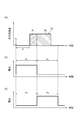
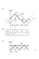
- FIG. 5A is a graph showing an example of a change over time of the intensity of reflected light incident on a certain pixel P (m, n).
- FIG. 5B is a graph showing a change with time of the voltage applied to the transfer electrode 11.
- FIG. 5C is a graph showing the change over time of the voltage applied to the transfer electrode 12.
- the reflected light L2 is delayed from the light irradiation timing T 1 for a time t corresponding to the distance to the object B is incident on the pixel P (m, n).
- the transfer electrode 11 is set to the on potential in the first period H 1 after the light irradiation, and is set to the off potential in the second period H 2 thereafter. Further, as shown in FIG. 5C, the transfer electrode 12 is set to the off potential in the first period H 1 and is set to the on potential in the second period H 2 . Then, it is assumed that a part of the reflected light L2 (region A 1 in the graph in the drawing) is incident on the pixel P (m, n) within the first period H 1 . At this time, since the transfer electrode 11 is set to the on potential while the transfer electrode 12 is set to the off potential, the charges generated in the photosensitive region 9a move to the charge collection region 9b and are accumulated.
- the remainder of the reflected light L2 enters the pixel P (m, n) within the second period H 2 .
- the transfer electrode 12 is set to the on potential while the transfer electrode 11 is set to the off potential, the charge generated in the photosensitive region 9a moves to the charge collection region 9c and is accumulated. Therefore, the amount of charge accumulated in the charge collection region 9b (the amount of charge of the storage node electrically coupled to the charge collection region 9b) and the amount of charge accumulated in the charge collection region 9c (electrical to the charge collection region 9c)
- the delay time t that is, the distance to the object B can be known.
- the processing circuit 8 of the present embodiment outputs a difference between these charge amounts by canceling out the charges in the charge collection region 9b and the charges accumulated in the charge collection region 9c. Also good. Even in such a case, if it is possible to know the total amount of charges accumulated in the charge collection regions 9b and 9c (total amount of charge of storage nodes respectively coupled to the charge collection regions 9b and 9c), It is possible to know the ratio between the amount of charge accumulated in the charge collection region 9b and the amount of charge accumulated in the charge collection region 9c.
- a driving method of the imaging region 5 (a driving method of the distance sensor according to the present embodiment) for knowing the total amount of charges accumulated in the charge collecting regions 9b and 9c will be described.
- the sensor drive circuit 7 drives the transfer electrodes 11 and 12 by sequentially executing a plurality of time-divided frames (each indicating a transfer electrode drive pattern).
- FIG. 6 is a diagram illustrating a driving method of the imaging region 5 by the sensor driving circuit 7. As shown in FIG. 6, in the driving method of the present embodiment, the processing in each frame F1, F2 is performed while the first frame F1 and the second frame F2 are alternately repeated. FIG. 6 also shows the processing contents in the frames F1 and F2.
- an accumulation frame F3 that performs charge accumulation in the charge collection regions 9b and 9c (charge accumulation in a storage node coupled to each of the charge collection regions 9b and 9c) and a charge collection region 9b and 9c
- the reading frames F4 for reading out the charges from are alternately repeated.
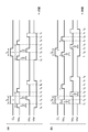
- FIGS. 7A and 7B are timing charts showing the operation of the transfer electrodes 11 to 13 in the storage frame F3.
- FIG. 7A shows a timing chart in the first frame F1
- FIG. 7B shows a timing chart in the second frame F2.
- the driving clock CL of the light source driving circuit 32 output from the control circuit 33 that is, the temporal change in the intensity of the pulsed light output from the light source 31
- the transfer electrode is shown.
- 11 shows a drive voltage Vtx 1 applied to the transfer electrode 11
- a drive voltage Vtx 2 applied to the transfer electrode 12 and a drive voltage Vtxr applied to the transfer electrode 13.
- the driving clock CL is at every rise once, the driving voltage Vtx 1 and Vtx 2 with a certain period T repeats the ON potential and OFF potential duplicate.
- the on-time of the drive voltages Vtx 1 and Vtx 2 in each cycle is equal to the on-time t L of the drive clock CL.
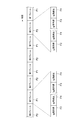
- the time t 0 , t 1 ,. ⁇ , t 9 is defined in the accumulated frames F3 of the first frame F1 and the second frame F2. These intervals are half of one irradiation time t L of the irradiation light L1. At this time, the light source unit 30 irradiates the irradiation light L1 between times t 1 and t 3 . Then, as shown in FIG. 7A, the sensor drive circuit 7 sets the drive voltage Vtx 1 to the on potential between time t 0 to t 2 and t 4 to t 6 in the first frame F1.
- the drive voltage Vtx 2 is set to the on potential during times t 2 to t 4 and t 6 to t 8 . Further, as shown in FIG. 7B, the sensor drive circuit 7 sets the drive voltage Vtx 1 to the on-potential between the times t 1 to t 3 and t 5 to t 7 in the second frame F2. Then, the drive voltage Vtx 2 is set to the on potential during times t 3 to t 5 and t 7 to t 9 .
- the drive voltage Vtxr applied to the transfer electrode 13 is set to the on-potential except during the period from when the other drive voltages Vtx 1 and Vtx 2 are first set to the on-potential to the last set to the off-potential. Is set. That is, the drive voltage Vtxr is set to the off potential during the time t 0 to t 8 in the first frame F1, is set to the off potential during the time t 1 to t 9 in the second frame F2, and the other period. At ON potential.
- the above operation is as follows.
- the drive voltage Vtx 1 rises at a timing earlier by (t L / 2) than the rise timing of the drive clock CL.
- the phase of the drive voltage Vtx 1 in the first frame F1 is set to 0 °.
- the drive voltage Vtx 2 rises at a timing later by t L than the rise timing of the drive voltage Vtx 1 .
- the phase of the drive voltage Vtx 2 in the first frame F1 is 180 °.
- the drive voltage Vtx 1 is rises at the same timing as the rising timing of the drive clock CL.
- the phase of the drive voltage Vtx 1 in the second frame F2 is 90 °.
- the drive voltage Vtx 2 rises at a timing later by t L than the rise timing of the drive voltage Vtx 1 .
- the phase of the drive voltage Vtx 2 in the second frame F2 is 270 °.
- FIG. 8 shows a timing chart with respect to one driving clock CL of the first frame F1 and the second frame F2 shown in FIGS. 7A and 7B in an overlapping manner.
- the drive voltage Vtx 1 (1) and the drive voltage Vtx 2 (1) respectively indicate the drive voltages Vtx 1 and Vtx 2 in the first frame F1, and the drive voltage Vtx 1 (2) and the drive voltage Vtx 2 (2) are respectively The drive voltages Vtx 1 and Vtx 2 in the second frame F2 are shown.
- FIG. 9 and 10 further show a chart of the received light pulse waveform of the reflected light L2 in the timing chart shown in FIG.
- the reflected light L2 is incident on the pixel P (m, n) after a time (t L / 3) from the irradiation of the light L1 onto the object B.
- the first frame F1 charges corresponding to the area of the region A 3 in FIG. 9 are stored in the charge collecting region 9b, and charges corresponding to the area of the region A 4 are stored in the charge collecting region 9c.
- the charge amount stored in the charge collection region 9b is Q / 6, and the charge amount stored in the charge collection region 9c is (5 ⁇ Q / 6).
- the charge amount stored in the charge collection region 9b is (2 ⁇ Q / 3), and the charge amount stored in the charge collection region 9c is Q / 3.
- the reflected light L2 is incident on the pixel P (m, n) after a time (3 ⁇ t L / 4) after the light L1 is irradiated on the object.
- the first frame F1 charges corresponding to the area of the region A 7 in the figure are stored in the charge collecting region 9b, and charges corresponding to the area of the region A 8 are stored in the charge collecting region 9c.
- the charge amount stored in the charge collection region 9b is Q / 4
- the charge amount stored in the charge collection region 9c is (3 ⁇ Q / 4).
- the charge amount stored in the charge collection region 9b is Q / 4
- the charge amount stored in the charge collection region 9c is (3 ⁇ Q / 4).
- phase 0 ° that is, times t 0 to t 2
- times t 4 to t 6 From the absolute value of the value obtained by subtracting the collected charge amount and the charge amount collected at phase 270 °, that is, times t 3 to t 5 , t 7 to t 9 , phase 90 °, that is, times t 1 to t 3 , t by adding the absolute value of the collected value obtained by subtracting the amount of charge in the 5 ⁇ t 7, it is possible to obtain a total charge Q generated by the reflected light L2.
- the ratio of the amount of charge accumulated in each of 9b and 9c (the ratio of the amount of charge accumulated in the storage nodes respectively coupled to the charge collection regions 9b and 9c) is obtained to know the delay time t, that is, the distance to the object B. be able to.
- FIG. 11A shows a value obtained by subtracting the charge amount of the storage node coupled to the charge collection region 9b from the charge amount of the storage node coupled to the charge collection region 9c (that is, from each pixel P (m, n). It is a graph which shows the relationship between output t) and time t (namely, distance to the target object B) after irradiating the light L1 until the reflected light L2 injects.
- the graph G11 shows the output value in the first frame F1
- the graph G12 shows the output value in the second frame F2.
- the output value is standardized so that the maximum value is 1 and the minimum value is -1.
- the output value increases from 0 to 1 in the section D 1 where 0 ⁇ t ⁇ t L / 2, and t L / 2 ⁇ t.
- the output value falls from 1 to 0, and in section D 3 where t L ⁇ t ⁇ (3 ⁇ t L / 2), the output value further falls from 0 to ⁇ 1 (3 Xt L / 2) ⁇ t ⁇ 2t
- the output value increases from ⁇ 1 to 0.
- the output value rises from ⁇ 1 to 0 in the section D 1 , the output value further rises from 0 to 1 in the section D 2 , and the section D 3 the output value is lowered from 1 to 0 in the output value in the section D 4 is further lowered from 0 to -1.
- the signs of the output values in the first frame F1 and the second frame F2 are ( ⁇ ) and (+) in the section D 1 , respectively, and in the section D 2 They are (+) and (+), respectively, (+) and ( ⁇ ) in the section D 3 , and ( ⁇ ) and ( ⁇ ) in the section D 4 , respectively. Therefore, based on the combination of the signs of the output values in the first frame F1 and the second frame F2, the time t from the irradiation of the light L1 to the incidence of the reflected light L2 is any of the sections D 1 to D 4 It can be determined whether it exists in the section.
- the absolute value of each output value of the first frame F1 and the second frame F2 is taken. Specifically, in the interval D 1 is inverted the sign of the output value of the second frame F2 (graph G12), the sign of the output value of the first frame F1 (graph G11) is inverted in the interval D 3, section in D 3 code of each output value is inverted in the first frame F1 and the second frame F2 (the graph of FIG G13, G14). Thereafter, by adding the absolute values of the output values of the first frame F1 and the second frame F2, a graph G21 having a constant value is obtained regardless of the time t. This graph G21 represents the total charge amount (the charge amount Q described above) generated by the reflected light L2.
- an appropriate offset value is added to the output value of the second frame F2 in the sections D 1 and D 2 and the output value of the second frame F2 in the sections D 3 and D 4 , respectively.
- a linear graph G22 in which the output value increases from 0 to 1 in the range of 0 ⁇ t ⁇ 2t L is obtained.
- the time t that is, the distance to the object B can be known based on the graph G21 and the graph G22.
- the order of the operations shown in FIGS. 12A to 12C is not limited to the above, and may be performed in a different order. Alternatively, the operations shown in FIGS. 12A to 12C may be performed simultaneously.
- the output value of the second frame F2 is used.
- the graph G22 of FIG. 12C is calculated using the output value of the first frame F1. Also good.
- the time t that is, the target object, based on the difference between the charge amounts accumulated in the accumulation nodes respectively coupled to the charge collection regions 9b and 9c.
- the distance to B can be obtained. Therefore, a usage method of injecting an equal amount of current into each storage node is possible, thereby avoiding saturation of each storage node.
- a circuit configuration example for injecting an equal amount of current into each storage node will be described in detail.
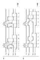
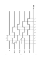
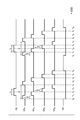
- FIG. 13 is a circuit diagram showing a detailed configuration of the current injection circuit 20 shown in FIG.
- the current injection circuit 20 of this embodiment includes a voltage generation circuit 21 and transistors 22a, 22b, 23a, and 23b.
- the transistors 22a, 22b, 23a, and 23b are field effect transistors such as p-channel MOSFETs.
- the voltage generation circuit 21 is connected between the power supply potential line 34 and a reference potential line GND having a lower potential than the power supply potential line 34.
- the voltage generation circuit 21 generates control voltages VC 1 and VC 2 corresponding to the larger charge amount among the charge amounts accumulated in the charge collection regions 9b and 9c.
- the voltage generation circuit 21 includes a transistor pair 24 and a current source 25 connected in series between the power supply potential line 34 and the reference potential line GND. Further, the voltage generation circuit 21 includes buffer circuits 27 and 28.
- the transistor pair 24 includes transistors 24a and 24b.
- the transistors 24a and 24b are field effect transistors such as p-channel MOSFETs.
- One current terminal (first current terminal) of each of the transistors 24 a and 24 b is short-circuited to each other and is electrically connected to the power supply potential line 34 via the current source 25.
- the other current terminals (second current terminals) of the transistors 24a and 24b are short-circuited to each other and are electrically connected to the reference potential line GND.
- the control terminal of the transistor 24a is electrically connected to the signal extraction electrode 15 on the charge collection region 9b via the storage node 26a.
- the control terminal of the transistor 24b is electrically connected to the signal extraction electrode 16 on the charge collection region 9c via the storage node 26b.
- the accumulation node 26a accumulates the collected charge in the charge collection region 9b, and the accumulation node 26b accumulates the collected charge in the charge collection region 9c.
- Current source 25 includes a transistor 25a.
- the transistor 25a is a field effect transistor such as a p-channel MOSFET.
- One current terminal (first current terminal) of the transistor 25 a is electrically connected to the power supply potential line 34.
- the other current terminal (second current terminal) of the transistor 25a is electrically connected to the first current terminal of each of the transistors 24a and 24b.
- a predetermined bias voltage V 1 is applied to the control terminal of the transistor 25a.
- the current source may further include another transistor connected in parallel with the transistor 25a.
- the transistor 22a supplies a current for removing the disturbance light component and avoiding the saturation of the storage node 26a to the storage node 26a.
- One current terminal (first current terminal) of the transistor 22a is connected to the power supply potential line 34, and the other current terminal (second current terminal) is connected to the storage node 26a via the transistor 23a.
- the control terminal of the transistor 22 a is electrically connected to a node N 1 between the transistor pair 24 and the current source 25 via the buffer circuit 27.
- the transistor 22b supplies a charge for removing the disturbance light component to the storage node 26b.
- One current terminal (first current terminal) of the transistor 22b is connected to the power supply potential line 34, and the other current terminal (second current terminal) is connected to the storage node 26b via the transistor 23b.
- the control terminal of the transistor 22 b is connected to the node N 1 through the buffer circuit 28.
- the transistor 23a is cascode-connected to the transistor 22a and suppresses fluctuations in the potential of the storage node 26a from affecting the operation of the transistor 22a. Specifically, one current terminal (first current terminal) of the transistor 23a is connected to the second current terminal of the transistor 22a, and the other current terminal (second current terminal) of the transistor 23a is stored. It is connected to the node 26a. A predetermined bias voltage V 3 is applied to the control terminal of the transistor 23a.
- the transistor 23b is cascode-connected to the transistor 22b and suppresses fluctuations in the potential of the storage node 26b from affecting the operation of the transistor 22b. Specifically, one current terminal (first current terminal) of the transistor 23b is connected to the second current terminal of the transistor 22b, and the other current terminal (second current terminal) of the transistor 23b is stored. It is connected to the node 26b. A predetermined bias voltage V 4 is applied to the control terminal of the transistor 23b. In one embodiment, the bias voltage V 3 and the bias voltage V 4 are equal to each other.
- the buffer circuit 27 generates a control voltage VC 1 by shifting the potential of the node N 1 and provides it to the control terminal of the transistor 22a.
- the buffer circuit 27 includes, for example, a source follower circuit. Specifically, the buffer circuit 27 includes transistors 27a and 27b connected in series with each other. One current terminal (first current terminal) of the transistor 27a is connected to the power supply potential line 34, and the other current terminal (second current terminal) is connected to one current terminal (first current terminal) of the transistor 27b. It is connected. The other current terminal (second current terminal) of the transistor 27b is connected to the reference potential line GND. A predetermined bias voltage V 5 is applied to the control terminal of the transistor 27a. The potential of the node N 1 is input to the control terminal of the transistor 27b.
- the buffer circuit 27 outputs a control voltage VC 1 having a magnitude corresponding to the potential of the node N 1 from a node between the transistors 27a and 27b.
- the buffer circuit 28 shifts the potential of the node N 1 to generate the control voltage VC 2 and provides it to the control terminal of the transistor 22b.
- the buffer circuit 28 includes, for example, a source follower circuit.
- the buffer circuit 28 includes transistors 28a and 28b connected in series with each other.
- One current terminal (first current terminal) of the transistor 28a is connected to the power supply potential line 34, and the other current terminal (second current terminal) is connected to one current terminal (first current terminal) of the transistor 28b. It is connected.
- the other current terminal (second current terminal) of the transistor 28b is connected to the reference potential line GND.
- a predetermined bias voltage V 6 is applied to the control terminal of the transistor 28a.
- the control terminal of the transistor 28b is the potential of the node N 1 is input.
- the buffer circuit 28 outputs a control voltage VC 2 having a magnitude corresponding to the potential of the node N 1 from a node between the transistors 28a and 28b.
- the magnitudes of the bias voltages V 5 and V 6 are set such that the amount of current supplied from the transistor 22a to the storage node 26a is equal to the amount of current supplied from the transistor 22b to the storage node 26b.
- V 5 V 6 may be sufficient.
- the buffer circuits 27 and 28 may be omitted.
- transistors 22a, 22b are each controlled terminal being connected directly to the node N 1, the potential of the node N 1 is provided to these control terminals as the control voltage VC 1, VC 2.
- the current injection circuit 20 further includes reset circuits 35 and 36.
- the reset circuit 35 has a transistor 35a
- the reset circuit 36 has a transistor 36a.
- the reset potential Vr is input to one current terminal (first current terminal) of the transistors 35a and 36a.
- the other current terminal (second current terminal) of the transistor 35a is connected to the storage node 26a, and the other current terminal (second current terminal) of the transistor 36a is connected to the storage node 26b.
- the reset signal Sr is input to the control terminals of the transistors 35a and 36a, and the transistors 35a and 36a are turned on, whereby the charges of the storage nodes 26a and 26b are discharged.
- the potentials of the storage nodes 26a and 26b become magnitudes corresponding to the amounts of charge flowing into the charge collection regions 9b and 9c, respectively.
- the accumulation frame F3 see FIG. 6
- the inflow of charges into the charge collection regions 9b and 9c continues, and when one of the accumulation nodes 26a and 26b exceeds the turn-on voltage, the transistors 24a and 24b One of them starts to flow a current corresponding to the potential of the one storage node. Therefore, the potential of the node N 1 has a magnitude corresponding to the larger one of the charge amounts stored in the charge collection regions 9b and 9c (storage nodes 26a and 26b).
- Control voltages VC 1 and VC 2 having a magnitude corresponding to the potential of the node N 1 are output to the control terminals of the transistors 22a and 22b.
- the transistors 22a and 22b receive the above-described control voltages VC 1 and VC 2 at their control terminals, and flow currents corresponding to the magnitudes of the control voltages VC 1 and VC 2 .
- predetermined bias voltages V 3 and V 4 are always applied to the control terminals of the transistors 23a and 23b, currents from the transistors 23a and 23b are injected into the storage nodes 26a and 26b, respectively.
- the same amount of charge is canceled in the storage nodes 26a and 26b, and saturation of the storage nodes 26a and 26b (charge collection regions 9b and 9c) due to disturbance light is avoided.
- the distance to the object B can be obtained based on the difference in the amount of charge accumulated in the accumulation nodes respectively coupled to the charge collection regions 9b and 9c. Therefore, a usage method in which an equal amount of current is injected into each storage node by the current injection circuit 20 becomes possible, thereby avoiding saturation of each storage node.
- the light emission state of the light source is intermittent in this embodiment, so that the intensity of irradiation light can be increased. That is, the intensity (ie, S / N ratio) of irradiation light with respect to the intensity of disturbance light can be increased. Further, when outputting intermittent light such as pulsed light as compared with continuous light such as triangular wave light, there is an advantage that the selectivity of the light source such as duty ratio and light quantity is high (selection is easy). .
- the distance sensor described in Patent Document 1 can measure only a distance corresponding to a delay time equal to the irradiation time of the irradiation light L1.
- the sensor drive circuit 7 may drive the transfer electrode 13 as described above in each of the frames F1 and F2.
- the transfer electrode 13 charges due to disturbance light can be discharged using the transfer electrode 13 except during a period in which the transfer electrodes 11 and 12 are driven. Therefore, further suppression of saturation due to disturbance light and reduction of shot noise due to disturbance light can be achieved, so that resistance to disturbance light and distance measurement accuracy can be improved.
- cascode devices such as transistors 23a and 23b are connected between the transistors 22a and 22b and the storage nodes 26a and 26b.
- the potentials of transistors 22a and 22b and storage nodes 26a and 26b are separated. Therefore, even if there is a potential difference between the storage node 26a and the storage node 26b, the influence on the drain-source voltages of the transistors 22a and 22b is suppressed, and the drain-source voltages of these transistors 22a and 22b are mutually reduced. Can be equal.
- the difference in the amount of current injected from the transistors 22a and 22b to the storage nodes 26a and 26b (charge collection regions 9b and 9c) is reduced, and these injected current amounts can be accurately controlled to be substantially equal. . Therefore, the error in outputting the difference between the charge amounts accumulated in the charge collection regions 9b and 9c in the processing circuit 8 can be reduced, and the accuracy of the measurement distance can be increased.
- FIG. 14A and FIG. 14B are diagrams showing a timing chart of the driving method according to the first modification of the embodiment.
- the sensor drive circuit 7 of the above embodiment is based on the timing charts shown in FIGS. 14 (a) and 14 (b) instead of the timing charts shown in FIGS. 7 (a) and 7 (b).
- the transfer electrodes 11 and 12 may be driven.
- the difference between the timing chart of the first modified example and the timing chart of the above embodiment is the length of the on time of the drive voltages Vtx 1 and Vtx 2 .
- the on-time of the drive voltages Vtx 1 and Vtx 2 is equal to the on-time of the drive clock CL (that is, the irradiation time of the irradiation light L1) t L , but in this first modified example, the drive voltages Vtx 1 and Vtx The on-time of 2 is half the time t L (t L / 2).
- time t 0 , t 1 ,. ⁇ , t 8 is defined in the accumulated frame F3 of each of the first frame F1 and the second frame F2. These intervals are half of one irradiation time t L of the irradiation light L1. At this time, the light source unit 30 irradiates the irradiation light L1 between times t 1 and t 3 . Then, as shown in FIG. 14A, the sensor drive circuit 7 sets the drive voltage Vtx 1 to the on potential between time t 0 to t 1 and t 4 to t 5 in the first frame F1.
- the drive voltage Vtx 2 is set to the on potential during times t 2 to t 3 and t 6 to t 7 .
- the sensor drive circuit 7 sets the drive voltage Vtx 1 to the on-potential between the times t 1 to t 2 and t 5 to t 6 in the second frame F2. Then, the drive voltage Vtx 2 is set to the on potential during times t 3 to t 4 and t 7 to t 8 .
- the drive voltage Vtxr applied to the transfer electrode 13 is set to the on-potential except during the period from when the other drive voltages Vtx 1 and Vtx 2 are first set to the on-potential to the last set to the off-potential. Is set. That is, the drive voltage Vtxr is set to the off potential during the time t 0 to t 7 in the first frame F1, is set to the off potential during the time t 1 to t 8 in the second frame F2, and the other period. At ON potential.
- FIGS. 15A to 15C are diagrams for explaining a distance calculation method in the first modification.
- FIG. 15A illustrates a value obtained by subtracting the charge amount of the storage node coupled to the charge collection region 9b from the charge amount of the storage node coupled to the charge collection region 9c (ie, from each pixel P (m, n). It is a graph which shows the relationship between output t) and time t (namely, distance to the target object B) after irradiating the light L1 until the reflected light L2 injects.
- a graph G41 shows an output value in the first frame F1
- a graph G42 shows an output value in the second frame F2.
- the output value is standardized so that the maximum value is 1 and the minimum value is -1.
- the output value is constant at 1 in the section D 1 where 0 ⁇ t ⁇ t L / 2, and t L / 2 ⁇ t ⁇ t L.
- the output value decreases from 1 to ⁇ 1 in the interval D 2 of the current period, and the output value becomes constant at ⁇ 1 in the interval D 3 of t L ⁇ t ⁇ (3 ⁇ t L / 2), and (3 ⁇ t L / 2) )
- the output value rises from ⁇ 1 to 1 in the interval D 4 where ⁇ t ⁇ 2t L.
- the output value rises from ⁇ 1 to 1 in the section D 1 , the output value becomes constant at 1 in the section D 2 , and the output value in the section D 3 down from 1 to -1, the output value in the section D 4 becomes constant at -1.
- the first frame F1 and the second frame F2 are sections in which the output value (graph G41) of the first frame F1 is smaller than the output value (graph G42) of the second frame F2.
- the sign having the smaller absolute value among the output values is inverted.
- the output value of the first frame F1, and the sign of the output value of the second frame F2 in the interval D 3 is inverted in the interval D 2.
- the output value of the second frame F2 in the sections D 1 and D 3 and the output value of the first frame F1 in the sections D 2 and D 4 both have a positive slope with respect to the time t.
- the distance to the object B is obtained based on the difference between the charge amounts accumulated in the accumulation nodes respectively coupled to the charge collection regions 9b and 9c, as in the above embodiment. Can do. Therefore, a usage method of injecting an equal amount of current into each storage node is possible, thereby avoiding saturation of each storage node. In addition, other effects of the above-described embodiment can be suitably achieved.
- the sensor driving circuit 7 may drive the transfer electrode 13 as described above in each of the frames F1 and F2. As a result, it is possible to further suppress saturation due to disturbance light and to reduce shot noise due to disturbance light, so that it is possible to improve resistance to disturbance light and distance measurement accuracy.
- FIG. 16 is a plan view showing a light receiving unit 9A according to a second modification of the embodiment.
- the light receiving unit 9A of the second modified example includes a transfer electrode 11 (first transfer electrode), a transfer electrode 12 (second transfer electrode), and a transfer electrode 51 (third transfer electrode). ) And one transfer electrode 52 (fourth transfer electrode).
- These transfer electrodes 11, 12, 51, 52 are arranged around the photogate electrode 14 along with the photogate electrode 14.
- the photogate electrode 14 is located between the transfer electrode 11 and the transfer electrode 12, and the photogate electrode 14 is located between the transfer electrode 51 and the transfer electrode 52.
- 11, 12, 51, 52 are aligned with the photogate electrode 14, there is no restriction on the positional relationship between them.
- the light receiving unit 9A has one signal extraction electrode 15, 16, 55, 56, respectively.
- the transfer electrode 11 is arranged between the signal extraction electrode 15 and the photogate electrode 14, the transfer electrode 12 is arranged between the signal extraction electrode 16 and the photogate electrode 14, and the transfer electrode 51 is arranged between the signal extraction electrode 55 and the photogate electrode 14.
- the transfer electrode 52 is disposed between the signal extraction electrode 56 and the photogate electrode 14.
- the light receiving unit 9 ⁇ / b> A includes a transfer electrode 13 and a charge discharging electrode 17.
- the configuration immediately below the transfer electrodes 11 and 12 and the signal extraction electrodes 15 and 16 is the same as in FIG. 3, and the configuration immediately below the transfer electrode 13 and the charge discharging electrode 17 is the same as in FIG. 17 is a cross-sectional view taken along the line XVII-XVII in FIG. 16, including the configuration immediately below the transfer electrodes 51 and 52 and the signal extraction electrodes 55 and 56.
- FIG. 17 the light receiving unit 9A further includes a charge collection region 9e (third charge collection region) and a charge collection region 9f (fourth charge collection region).
- the charge collection regions 9e and 9f are arranged so as to be adjacent to the photosensitive region 9a with the photosensitive region 9a interposed therebetween, collect charges from the photosensitive region 9a, and store them in the respective storage nodes.
- the configuration of the charge collection regions 9e and 9f is the same as the configuration of the charge collection regions 9b and 9c shown in FIG.
- the signal extraction electrode 55 is formed on the charge collection region 9e, and the signal extraction electrode 56 is formed on the charge collection region 9f.
- the signal extraction electrodes 55 and 56 are in contact with the charge collection regions 9e and 9f through the openings formed in the insulating layer 41.
- the transfer electrode 51 is disposed on a region between the photosensitive region 9a and the charge collection region 9e.
- the transfer electrode 52 is disposed on a region between the photosensitive region 9a and the charge collection region 9f.
- FIG. 18 is a diagram illustrating a driving method of the sensor driving circuit in the second modification.
- the process in the frame F5 is performed while the same frame F5 is repeated.
- FIG. 18 also shows the processing contents in the frame F5.
- the accumulation frame F6 for accumulating charges in the accumulation nodes respectively coupled to the charge collection regions 9b, 9c, 9e, and 9f, and reading out the charges from the charge collection regions 9b, 9c, 9e, and 9f.
- the readout frame F4 to be performed is repeated alternately.
- FIG. 19 is a timing chart showing the operation of the transfer electrodes 11, 12, 13, 51, 52 in the storage frame F6.
- the drive clock CL the drive voltage Vtx 1 applied to the transfer electrode 11, the drive voltage Vtx 2 applied to the transfer electrode 12, the drive voltage Vtx 3 applied to the transfer electrode 51, and the transfer A drive voltage Vtx 4 applied to the electrode 52 and a drive voltage Vtxr applied to the transfer electrode 13 are shown.
- the drive voltages Vtx 1 to Vtx 4 are repeatedly turned on and off twice with a certain period T.
- the on-time of the drive voltages Vtx 1 to Vtx 2 in each cycle is half of the on-time t L of the drive clock CL (t L / 2).
- equidistant times t 0 , t 1 ,..., T 8 are defined in the accumulation frame F 6 of each frame F 5. These intervals are half of one irradiation time t L of the irradiation light L1. At this time, the light source unit 30 irradiates the irradiation light L1 between times t 1 and t 3 . Then, as shown in FIG. 19, equidistant times t 0 , t 1 ,..., T 8 are defined in the accumulation frame F 6 of each frame F 5. These intervals are half of one irradiation time t L of the irradiation light L1. At this time, the light source unit 30 irradiates the irradiation light L1 between times t 1 and t 3 . Then, as shown in FIG.
- the sensor drive circuit 7 sets the drive voltage Vtx 1 to the on potential during the times t 0 to t 1 and t 4 to t 5 , and the drive voltage Vtx 2 Is set to the on potential between times t 1 to t 2 and t 5 to t 6 , the drive voltage Vtx 3 is set to the on potential between times t 2 to t 3 and t 6 to t 7 , and the drive voltage Vtx 4 is set. Is set to the on potential during times t 3 to t 4 and t 7 to t 8 .
- the drive voltage Vtxr applied to the transfer electrode 13 is set to the on-potential except during a period from when the other drive voltages Vtx 1 to Vtx 4 are first set to the on-potential to the last set to the off-potential. Is set. That is, the drive voltage Vtxr is set to the off potential during the times t 0 to t 8 in each frame F5, and is set to the on potential during the other periods.
- the second modification is an example in which the first frame F1 and the second frame F2 of the first modification are collectively executed in one frame F5. Therefore, the distance calculation method in the second modification is the same as the distance calculation method in the first modification (see FIGS. 15A to 15C). That is, the output value of the first frame F1 in the first modification example is changed from the charge amount of the storage node connected to the charge collection area 9c to the charge quantity of the storage node connected to the charge collection area 9b in this second modification example.
- the output value of the second frame F2 in the first modification is used as the subtracted value, and in this second modification, the charge amount of the storage node coupled to the charge collection region 9f is changed to the value of the storage node coupled to the charge collection region 9e.
- a value obtained by subtracting the amount of charge is preferable.
- the difference between the charge amounts accumulated in the storage nodes respectively coupled to the charge collection regions 9b and 9c and the charge collection regions 9e and 9f are coupled to each other. Based on the difference in the amount of charge accumulated in the accumulation node, the distance to the object B can be obtained. Therefore, a usage method of injecting an equal amount of current into each storage node is possible, thereby avoiding saturation of each storage node. In addition, other effects of the above-described embodiment can be suitably achieved.
- the sensor drive circuit 7 may drive the transfer electrode 13 in each frame F5 as described above. As a result, it is possible to further suppress saturation due to disturbance light and to reduce shot noise due to disturbance light, so that it is possible to improve resistance to disturbance light and distance measurement accuracy.
- each transistor of the sensor driving circuit is a MOSFET is illustrated, but each transistor may be another FET or a bipolar transistor.
- SYMBOLS 1A ... Distance sensor, 3 ... Semiconductor substrate, 5 ... Imaging area, 7 ... Sensor drive circuit, 8 ... Processing circuit, 9, 9A ... Light receiving part, 9a ... Photosensitive area, 9b-9f ... Charge collection area, 11, 12 , 13, 51, 52... Transfer electrode, 14... Photogate electrode, 15, 16, 55, 56... Signal extraction electrode, 17... Charge discharging electrode, 20.
Landscapes
- Engineering & Computer Science (AREA)
- Physics & Mathematics (AREA)
- General Physics & Mathematics (AREA)
- Radar, Positioning & Navigation (AREA)
- Remote Sensing (AREA)
- Electromagnetism (AREA)
- Computer Networks & Wireless Communication (AREA)
- Signal Processing (AREA)
- Multimedia (AREA)
- Optical Radar Systems And Details Thereof (AREA)
- Measurement Of Optical Distance (AREA)
- Transforming Light Signals Into Electric Signals (AREA)
- Solid State Image Pick-Up Elements (AREA)
Abstract
本発明は、光感応領域の電荷が第1および第2の転送電極(11,12)の駆動により振り分けられる電荷収集領域(9b,9c)にそれぞれ結合された蓄積ノードに等量の電流を注入する一方、蓄積ノードそれぞれの電荷量の差分情報に基づいて対象物までの距離を求める距離センサに関する。蓄積ノードそれぞれに等量の電流を注入することにより各蓄積ノードの外乱光に起因した飽和が回避される一方、電極駆動パターンをそれぞれ示す複数フレームに従って第1および第2の転送電極(11,12)を駆動させることにより、電流注入の影響を受けにくい、蓄積ノードそれぞれの電荷量の差分情報が得 られる。
Description
本発明は、距離センサおよび距離センサの駆動方法に関するものである。
光源から光を放出したタイミングと、対象物からの反射光が到達したタイミングとの時間差に基づいて、対象物までの距離を測定する飛行時間(TOF:Time-of-Flight)法が知られている。例えば、下記の特許文献1には、TOF法に基づく距離センサが記載されている。この特許文献1に記載された距離センサは、電荷振分け型の構成を備えており、パルス状の光を照射した後の第1の期間に発生する電荷と、第1の期間後の第2の期間に発生する電荷とが、それぞれ異なる電荷収集領域に結合された蓄積ノードに蓄積される。そして、これらの蓄積ノードに蓄積された電荷量の比に基づいて、対象物までの距離を算出する。
また、非特許文献1には、三角波状の光を照射し、照射光とその反射光との位相差に基づいて、対象物までの距離を測定する方法が記載されている。
David Stoppa et al., Introduction to 3D Time-of -Flight Image Sensors, European Solid-State Circuits Conference (ESSCIRC), European Solid-State Device Conference (ESSDERC), 2015
発明者らは、上述の従来技術について検討した結果、以下のような課題を発見した。すなわち、距離センサにおいては、一般に、反射光による電荷のみでなく、外乱光による電荷も蓄積ノードに蓄積される。特許文献1に記載された距離センサでは、距離の算出を行う際に、蓄積ノードそれぞれにおいて得られた電荷量から外乱光に相当する電荷量が差し引かれる。したがって、反射光による電荷と外乱光による電荷とが共に蓄積ノードそれぞれに蓄積され、蓄積ノードが飽和し易くなるという課題があった。なお、特許文献1に記載された方法では、パルス状の光が出力されるので、外乱光の強さに対する照射光の強度(すなわちS/N比)を高くすることができるという利点がある。
また、非特許文献1に記載された方法では、三角波状の光が対象物に照射されるので、その1周期の間に発生する電荷をすべて取り込むためには、1周期の間、常にいずれかの転送電極がオン電位(電荷転送を可能にする電位)に設定される必要がある。この場合、外乱光による電荷を多く取り込むこととなり、蓄積ノードそれぞれが飽和し易くなる。また、パルス状の光が出力される場合と比較して、光源の発光状態が連続するので、照射光の強度が低く抑えられ、外乱光の強さに対する照射光の強度(すなわちS/N比)が低いという課題があった。
ここで、蓄積ノードの飽和を回避するために、各蓄積ノードに電流を注入して電荷を打ち消すことが考えられる。そのような方式では、外乱光の強度が不明な状態で電流注入を行う必要があるため、各蓄積ノードに等量の電流を注入するとともに、蓄積ノードそれぞれに蓄積された電荷量の差分により対象物までの距離を求め得ることが望まれる。電荷量の差分であれば、注入された電流の影響を受けないからである。しかしながら、上記特許文献1および非特許文献1に記載された距離センサでは、そのような方法での使用が困難である。
本発明は、上述のような課題を解決するためになされたものであり、光感応領域の電荷が複数の転送電極の駆動により振り分けられる電荷収集領域にそれぞれ電気的に結合された蓄積ノードに等量の電流を注入する一方、蓄積ノードそれぞれの電荷量の差分情報に基づいて対象物までの距離を求めることを可能にするための構造を備えた距離センサおよび距離センサの駆動方法を提供することを目的としている。
本実施形態に係る距離センサは、対象物に光を照射し、該対象物からの反射光を検出することにより該対象物までの距離を計測する距離センサであって、その一態様として、光照射部と、半導体基板と、第1の転送電極と、第2の転送電極と、駆動部と、を備える。光照射部は、パルス状の光を対象物に繰り返し照射する。半導体基板は、光感応領域と、第1および第2の電荷収集領域と、を有する。光感応領域は、反射光の光量に応じた電荷を発生する領域である。第1および第2の電荷収集領域それぞれは、光感応領域から所定距離離間した状態で配置され、該光感応領域からの電荷を収集する領域である。第1の転送電極は、光感応領域と第1の電荷収集領域との間の領域上に配置され、オン電位またはオフ電位に設定可能な電極である。ここで、オン電位は、光感応領域から第1の電荷収集領域への電荷転送を可能にする電位であり、オフ電位は、この電荷転送を停止させる電位である。第2の転送電極は、光感応領域と前記第2の電荷収集領域との間の領域上に配置され、光感応領域から第2の電荷収集領域への電荷転送を可能にする電位であり、オフ電位は、この電荷転送を停止させる電位である。駆動部は、それぞれが、第1および第2の転送電極を駆動させるための電極駆動パターンを構成するとともに等間隔の時刻t0、t1、・・・、t9で定義された複数のフレームを順に実行することにより、これら第1および第2の転送電極を駆動させる。上述のような構成において、光照射部は、複数のフレームそれぞれにおいて光を時刻t1~t3の間照射する。また、駆動部は、複数のフレームのうちの第1フレームにおいて、第1の転送電極を時刻t0~t2およびt4~t6の間オン電位に設定する一方、第2の転送電極を時刻t2~t4およびt6~t8の間オン電位に設定する。更に、駆動部は、第1フレームとは別の第2フレームにおいて、第1の転送電極を時刻t1~t3およびt5~t7の間オン電位に設定する一方、第2の転送電極を時刻t3~t5およびt7~t9の間オン電位に設定する。
本実施形態に係る距離センサは、パルス状の光を対象物に照射する距離センサであって、光感応領域の電荷が複数の転送電極の駆動により振り分けられる電荷収集領域にそれぞれ電気的に結合された蓄積ノードに等量の電流を注入する一方、蓄積ノードそれぞれの電荷量の差分情報に基づいて対象物までの距離を求めるための構造を有する。そのため、当該距離センサおよび当該距離センサを駆動対象とする駆動方法によれな、蓄積ノードそれぞれに等量の電流を注入することにより各蓄積ノードの外乱光に起因した飽和が回避される一方、電極駆動パターンをそれぞれ示す複数フレームに従って第1および第2の転送電極を駆動させることにより、電流注入の影響を受けにくい、蓄積ノードそれぞれの電荷量の差分情報が得られる。
[本願発明の実施形態の説明]
最初に本願発明の実施形態の対応それぞれを個別に列挙して説明する。
最初に本願発明の実施形態の対応それぞれを個別に列挙して説明する。
(1)本実施形態に係る距離センサは、対象物に光を照射し、該対象物からの反射光を検出することにより該対象物までの距離を計測する距離センサであって、その一態様として、光照射部と、半導体基板と、第1の転送電極と、第2の転送電極と、駆動部と、を備える。光照射部は、パルス状の光を対象物に繰り返し照射する。半導体基板は、光感応領域と、第1および第2の電荷収集領域と、を有する。光感応領域は、反射光の光量に応じた電荷を発生する領域である。第1および第2の電荷収集領域それぞれは、光感応領域から所定距離離間した状態で配置され、該光感応領域からの電荷を収集する領域である。第1の転送電極は、光感応領域と第1の電荷収集領域との間の領域上に配置され、オン電位またはオフ電位に設定可能な電極である。ここで、オン電位は、光感応領域から第1の電荷収集領域への電荷転送を可能にする電位であり、オフ電位は、この電荷転送を停止させる電位である。第2の転送電極は、光感応領域と前記第2の電荷収集領域との間の領域上に配置され、光感応領域から第2の電荷収集領域への電荷転送を可能にする電位であり、オフ電位は、この電荷転送を停止させる電位である。駆動部は、それぞれが、第1および第2の転送電極を駆動させるための電極駆動パターンを構成するとともに等間隔の時刻t0、t1、・・・、t9で定義された複数のフレームを順に実行することにより、これら第1および第2の転送電極を駆動させる。上述のような構成において、光照射部は、複数のフレームそれぞれにおいて光を時刻t1~t3の間照射する。また、駆動部は、複数のフレームのうちの第1フレームにおいて、第1の転送電極を時刻t0~t2およびt4~t6の間オン電位に設定する一方、第2の転送電極を時刻t2~t4およびt6~t8の間オン電位に設定する。更に、駆動部は、第1フレームとは別の第2フレームにおいて、第1の転送電極を時刻t1~t3およびt5~t7の間オン電位に設定する一方、第2の転送電極を時刻t3~t5およびt7~t9の間オン電位に設定する。
(2)本実施形態の一態様として、当該距離センサにおける上記駆動部は、それぞれが、第1および第2の転送電極を駆動させるための電極駆動パターンを構成するとともに等間隔の時刻t0、t1、・・・、t8で定義された複数のフレームを順に実行することにより、これら第1および第2の転送電極を駆動させてもよい。この場合、光照射部は、複数のフレームそれぞれにおいて光を時刻t1~t3の間照射する。駆動部は、複数のフレームのうちの第1フレームにおいて、第1の転送電極を時刻t0~t1およびt4~t5の間オン電位に設定する一方、第2の転送電極を時刻t2~t3およびt6~t7の間オン電位に設定する。更に、駆動部は、第1フレームとは別の第2フレームにおいて、第1の転送電極を時刻t1~t2およびt5~t6の間オン電位に設定する一方、第2の転送電極を時刻t3~t4およびt7~t8の間オン電位に設定する。
(3)本実施形態の一態様として、当該距離センサは、光照射部と、半導体基板と、第1~第4の転送電極と、駆動部と、を備えてもよい。光照射部は、パルス状の光を対象物に繰り返し照射する。半導体基板は、光感応領域と、第1~第4の電荷収集領域と、を有する。ここで、光感応領域は、反射光の光量に応じた電荷を発生する。第1~第4の電荷収集領域は、それぞれが光感応領域から所定距離離間した状態で配置され、該光感応領域からの電荷を収集する。第1の転送電極は、光感応領域と第1の電荷収集領域との間の領域上に配置され、第2の転送電極は、光感応領域と第2の電荷収集領域との間の領域上に配置され、第3の転送電極は、光感応領域と第3の電荷収集領域との間の領域上に配置され、第4の転送電極は、光感応領域と第4の電荷収集領域との間の領域上に配置される。第1~第4の転送電極のそれぞれは、光感応領域から対応する電荷収集領域への電荷転送を可能にするオン電位、または、この電荷転送を停止させるオフ電位に設定可能な電極である。駆動部は、それぞれが、第1~第4の転送電極を駆動させるための電極駆動パターンを構成するとともに等間隔の時刻t0、t1、・・・、t8で定義された複数のフレームを順に実行することにより、これら第1~第4の転送電極を駆動させる。上述のような構成において、光照射部は、複数のフレームそれぞれにおいて光を時刻t1~t3の間照射する。駆動部は、複数のフレームそれぞれにおいて、第1の転送電極を時刻t0~t1およびt4~t5の間オン電位に設定し、第2の転送電極を時刻t1~t2およびt5~t6の間オン電位に設定し、第3の転送電極を時刻t2~t3およびt6~t7の間オン電位に設定し、第4の転送電極を時刻t3~t4およびt7~t8の間オン電位に設定する。
(4)本実施形態に係る距離センサの駆動方法は、対象物に光を照射し、該対象物からの反射光を検出することにより該対象物までの距離を計測する距離センサを駆動する。駆動対象となる距離センサは、光照射部と、半導体基板と、第1の転送電極と、第2の転送電極と、を備える。光照射部は、パルス状の光を対象物に繰り返し照射する。半導体基板は、光感応領域と、第1および第2の電荷収集領域と、を有する。光感応領域は、反射光の光量に応じた電荷を発生する領域である。第1および第2の電荷収集領域それぞれは、光感応領域から所定距離離間した状態で配置され、該光感応領域からの電荷を収集する領域である。第1の転送電極は、光感応領域と第1の電荷収集領域との間の領域上に配置され、オン電位またはオフ電位に設定可能な電極である。ここで、オン電位は、光感応領域から第1の電荷収集領域への電荷転送を可能にする電位であり、オフ電位は、この電荷転送を停止させる電位である。第2の転送電極は、光感応領域と前記第2の電荷収集領域との間の領域上に配置され、光感応領域から第2の電荷収集領域への電荷転送を可能にする電位であり、オフ電位は、この電荷転送を停止させる電位である。当該駆動方法は、その一態様として、それぞれが、第1および第2の転送電極を駆動させるための電極駆動パターンを構成するとともに等間隔の時刻t0、t1、・・・、t9で定義された複数のフレームを順に実行する。具体的に、当該駆動方法では、複数のフレームそれぞれにおいて光照射部から光が時刻t1~t3の間照射される。また、当該駆動方法では、複数のフレームのうちの第1フレームにおいて、第1の転送電極が時刻t0~t2およびt4~t6の間オン電位に設定される一方、第2の転送電極が時刻t2~t4およびt6~t8の間オン電位に設定される。更に、当該駆動方法では、第1フレームとは別の第2フレームにおいて、第1の転送電極が時刻t1~t3およびt5~t7の間オン電位に設定される一方、第2の転送電極が時刻t3~t5およびt7~t9の間オン電位に設定される。
(5)本実施形態の一態様として、当該駆動方法は、上述のような構造を有する距離センサを駆動対象とし、それぞれが、第1および第2の転送電極を駆動させるための電極駆動パターンを構成するとともに等間隔の時刻t0、t1、・・・、t8で定義された複数のフレームを順に実行してもよい。この場合、当該駆動方法では、複数のフレームそれぞれにおいて光照射部から光が各フレームの時刻t1~t3の間照射される。また、当該駆動方法では、複数のフレームのうちの第1フレームにおいて、第1の転送電極が時刻t0~t1およびt4~t5の間オン電位に設定される一方、第2の転送電極が時刻t2~t3およびt6~t7の間オン電位に設定される。更に、当該駆動方法では、第1フレームとは別の第2フレームにおいて、第1の転送電極が時刻t1~t2およびt5~t6の間オン電位に設定される一方、第2の転送電極が時刻t3~t4およびt7~t8の間オン電位に設定される。
(6)本実施形態の一態様として、当該駆動方法の駆動対象となる距離センサは、光照射部と、半導体基板と、第1~第4の転送電極と、を備えてもよい。光照射部は、パルス状の光を対象物に繰り返し照射する。半導体基板は、光感応領域と、第1~第4の電荷収集領域と、を有する。ここで、光感応領域は、反射光の光量に応じた電荷を発生する。第1~第4の電荷収集領域は、それぞれが光感応領域から所定距離離間した状態で配置され、該光感応領域からの電荷を収集する。第1の転送電極は、光感応領域と第1の電荷収集領域との間の領域上に配置され、第2の転送電極は、光感応領域と第2の電荷収集領域との間の領域上に配置され、第3の転送電極は、光感応領域と第3の電荷収集領域との間の領域上に配置され、第4の転送電極は、光感応領域と第4の電荷収集領域との間の領域上に配置される。第1~第4の転送電極のそれぞれは、光感応領域から対応する電荷収集領域への電荷転送を可能にするオン電位、または、この電荷転送を停止させるオフ電位に設定可能な電極である。上述のような構造を有する距離センサを駆動対象とする当該駆動方法は、それぞれが、第1~第4の転送電極を駆動させるための電極駆動パターンを構成するとともに等間隔の時刻t0、t1、・・・、t8で定義された複数のフレームを順に実行する。具体的に、当該駆動方法では、複数のフレームそれぞれにおいて、光照射部から光が時刻t1~t3の間照射され、第1の転送電極が時刻t0~t1およびt4~t5の間オン電位に設定され、第2の転送電極が時刻t1~t2およびt5~t6の間オン電位に設定され、第3の転送電極が時刻t2~t3およびt6~t7の間オン電位に設定され、第4の転送電極が時刻t3~t4およびt7~t8の間オン電位に設定される。
(7)上記の種々の態様それぞれに係る距離センサおよび駆動方法によれば、後述する実施形態において述べるとおり、各蓄積ノードに蓄積された電荷量の差分により距離を求めることができる。従って、各蓄積ノードに等量の電流を注入することによって各蓄積ノードの飽和を回避することが可能になる。
(8)本実施形態に係る距離センサおよびその九度追う方法それぞれの一態様として、半導体基板は、光感応領域から所定距離離間した状態で配置された、該光感応領域からの電荷を収集する第5の電荷収集領域を更に有してもよく、この構成に対応して、距離センサは、光感応領域と第5の電荷収集領域との間の領域上に配置された第5の転送電極を更に備えてもよい。この場合、距離センサでは、駆動部が、第5の転送電極を、他の転送電極が最初にオン電位に設定されてから最後にオフ電位に設定されるまでの期間を除いて、オン電位に設定する。一方、駆動方法では、第5の転送電極が、他の転送電極が最初にオン電位に設定されてから最後にオフ電位に設定されるまでの期間を除いてオン電位に設定される。
(9)上記の種々の態様それぞれに係る距離センサおよび駆動方法によれば、第1および第2の転送電極(若しくは第1~第4の転送電極)が駆動している期間以外では第5の転送電極を用いて外乱光による電荷を排出することができる。従って、外乱光による飽和の更なる抑制、および外乱光によるショットノイズの低減が可能となるので、外乱光に対する耐性および測距精度をより向上させることができる。
以上、この[本願発明の実施形態の説明]の欄に列挙された各態様は、残りの全ての態様のそれぞれに対して、または、これら残りの態様の全ての組み合わせに対して適用可能である。
[本願発明の実施形態の詳細]
以下、本実施形態に係る距離センサおよび距離センサの駆動方法の具体的な構造を、添付図面を参照しながら詳細に説明する。なお、本発明はこれらの例示に限定されるものではなく、特許請求の範囲によって示され、特許請求の範囲と均等の意味および範囲内での全ての変更が含まれることが意図される。また、図面の説明において同一の要素には同一の符号を付し、重複する説明を省略する。
以下、本実施形態に係る距離センサおよび距離センサの駆動方法の具体的な構造を、添付図面を参照しながら詳細に説明する。なお、本発明はこれらの例示に限定されるものではなく、特許請求の範囲によって示され、特許請求の範囲と均等の意味および範囲内での全ての変更が含まれることが意図される。また、図面の説明において同一の要素には同一の符号を付し、重複する説明を省略する。
図1は、本発明の一実施形態に係る距離センサ1Aの構成を示す平面図である。距離センサ1Aは、対象物に光を照射し、該対象物からの反射光を検出することにより対象物までの距離を計測する。図1に示されたように、距離センサ1Aは、半導体基板3上に形成された撮像領域5と、センサ駆動回路7(駆動部)と、処理回路8と、を備える。センサ駆動回路7は、撮像領域5を駆動する。処理回路8は、撮像領域5の出力を処理する。撮像領域5は、半導体基板3上に一次元または二次元状に配列された複数の画素Pを備える。図1では、第m行第n列の画素P(m,n)が示されている(m,nは自然数)。各画素P(m,n)は、受光部9と、電流注入回路20とを含む。撮像領域5は、対象物からの反射光を画素Pごとに検出する。そして、光が照射されてから反射光が到達するまでの時間を画素Pごとに求めることにより、対象物の画像の画素Pごとの距離が求められる。当該距離センサ1Aは、電荷振分け型の距離センサであって、光が照射されてから反射光が到達するまでの時間を、各画素P内で2カ所に振り分けられた電荷量の比率に応じて求める。
図2は、図1に示された距離センサ1Aの各画素P(m,n)の受光部9の平面図である。図3および図4は、それぞれ図2のIII-III線およびIV-IV線に沿った断面図であって、受光部9の断面構成を示す。なお、図3には、光源ユニット30が併せて示されている。
図2に示されたように、本実施形態の受光部9は、転送電極11(第1の転送電極)と、転送電極12(第2の転送電極)と、転送電極13(第5の転送電極)と、フォトゲート電極14と、信号取出電極15,16と、電荷排出用電極17と、を有する。なお、図2では転送電極11,12および信号取出電極15,16がそれぞれ2個ずつ設けられているが、これらはそれぞれ1個ずつ設けられてもよい。また、図2では転送電極13および電荷排出用電極17が2個ずつ設けられているが、これらは1個ずつ設けられてもよい。
図3に示されたように、受光部9は、光感応領域9aと、電荷収集領域9b(第1の電荷収集領域)と、電荷収集領域9c(第2の電荷収集領域)とを更に有する。光感応領域9aは、反射光L2を受けてその光量に応じた電荷を発生する。電荷収集領域9b,9cは、光感応領域9aを挟んだ状態で該光感応領域9aに隣接するようそれぞれ配置されている。電荷収集領域9b,9cそれぞれが光感応領域9aからの電荷を収集することで、それぞれに結合された蓄積ノードに電荷が蓄積する。なお、図3では、電荷収集領域9b,9cの間に光感応領域9aが配置されているが、電荷収集領域9b,9cは、光感応領域9aの一方の側に隣接してもよく、互いの位置関係に制約は無い。
具体的には、半導体基板3は高濃度のp型(第2導電型)半導体からなり、各画素P(m,n)の受光部9は、半導体基板3の表面3a側に設けられた低濃度のp型(第2導電型)の表面領域3cを有する。また、半導体基板3の表面3a上には絶縁層41が形成されており、電荷収集領域9b,9c間の表面領域3c上にはフォトゲート電極14が絶縁層41を介して形成されている。フォトゲート電極14の直下に位置する表面領域3c内の領域が、光感応領域9aとなる。光感応領域9aのポテンシャルは、フォトゲート電極14への印加電圧によって制御される。フォトゲート電極14には、必要に応じてわずかな正の直流電圧が印加される。これにより、光感応領域9aへの光の入射に応じて正孔電子対が発生する。
電荷収集領域9b,9cは、半導体基板3の表面領域3c側に形成された高濃度のn型(第1導電型)領域である。電荷収集領域9b,9cは、フローティングディフュージョン領域あるいは電荷蓄積領域とも呼ばれる。n型半導体は、電気的に中性の状態で電子をキャリアとして有しており、キャリアが抜けた場合には、正にイオン化する。すなわち、高濃度のn型の電荷収集領域9b,9cのバンド構造は、大きく下向きに凹む形となり、ポテンシャル井戸を構成する。信号取出電極15は電荷収集領域9b上に形成されており、信号取出電極16は電荷収集領域9c上に形成されている。信号取出電極15,16は、絶縁層41に形成された開口を介して、各電荷収集領域9b,9cに接触している。
転送電極11は、光感応領域9aと電荷収集領域9bとの間の領域上に配置される。転送電極12は、光感応領域9aと電荷収集領域9cとの間の領域上に配置される。転送電極11に正電位(オン電位)が与えられると、転送電極11の直下の領域のポテンシャルが、光感応領域9aのポテンシャルと電荷収集領域9bのポテンシャルとの中間の大きさとなる。これにより、光感応領域9aから電荷収集領域9bへのポテンシャルの階段が形成され、電荷収集領域9bのポテンシャル井戸内に電子が落ち込むことになる(井戸内に電荷が蓄積される)。同様に、転送電極12に正電位(オン電位)が与えられると、転送電極12の直下の領域のポテンシャルが、光感応領域9aのポテンシャルと電荷収集領域9cのポテンシャルとの中間の大きさとなる。従って、光感応領域9aから電荷収集領域9cへのポテンシャルの階段が形成され、電荷収集領域9cのポテンシャル井戸内に電子が落ち込む。
なお、本実施形態では、電荷収集領域9b,9c上に信号取出電極15,16を設けて信号を取り出す構造を採用しているが、電荷収集領域9b,9cの隣に信号取り出し用の高濃度領域を別途設け、この高濃度領域と電荷収集領域9b,9cとの間の領域上に別の転送電極を配置し、高濃度領域上に信号取出電極を設けて信号を取り出すことも可能である。
光源ユニット30は、対象物Bに光L1を照射するための光照射部であって、光源31と、光源駆動回路32と、制御回路33と、を備える。光源31は、レーザ素子または発光ダイオードといった半導体発光素子を含む。光源駆動回路32は、光源31を高周波駆動する。制御回路33は、光源駆動回路32の駆動クロックを出力する。また、光源31からは、方形波の強度変調が行われたパルス光が対象物Bに対して周期的に繰り返し照射される。
光源31からの照射光L1は、対象物Bの表面にて反射し、反射光L2として距離センサ1Aの撮像領域5内の画素P(m,n)それぞれに半導体基板3の裏面3b側から入射する。なお、半導体基板3の裏面3bと対向して、画素P(m,n)それぞれに対応する複数の結像レンズが配置されてもよい。
図4に示されたように、受光部9は、2つの電荷収集領域9d(第5の電荷収集領域)を更に有する。電荷収集領域9dは、半導体基板3の表面領域3cに形成されており、光感応領域9aを挟んだ状態で該光感応領域9aに隣接するよう配置されている。そして、電荷排出用電極17はこの電荷収集領域9d上に形成されている。電荷排出用電極17は、絶縁層41に形成された開口を介して、電荷収集領域9dに接触している。転送電極13は、光感応領域9aと電荷収集領域9dとの間の領域上に配置される。転送電極13に正電位(オン電位)が与えられると、光感応領域9aから電荷収集領域9dへ電荷が移動し、電荷収集領域9dのポテンシャル井戸内に電荷が蓄積される。なお、電荷収集領域9dの具体的な構成は、電荷収集領域9b,9cと同様である。
図5(a)は、或る画素P(m,n)に入射する反射光の強度の時間変化の例を示すグラフである。図5(b)は、転送電極11に印加される電圧の時間変化を示すグラフである。図5(c)は、転送電極12に印加される電圧の時間変化を示すグラフである。図5(a)に示されるように、反射光L2は、光照射タイミングT1から対象物Bまでの距離に応じた時間tだけ遅延して画素P(m,n)に入射する。
図5(b)に示されたように、転送電極11は、光照射後の第1の期間H1にオン電位に設定され、その後の第2の期間H2にオフ電位に設定される。また、図5(c)に示されたように、転送電極12は、第1の期間H1にオフ電位に設定され、第2の期間H2にオン電位に設定される。そして、反射光L2の一部(図中のグラフの領域A1)が、第1の期間H1内に画素P(m,n)に入射したとする。このとき、転送電極11がオン電位に設定される一方、転送電極12がオフ電位に設定されているので、光感応領域9aにおいて発生した電荷は、電荷収集領域9bに移動し、蓄積される。反射光L2の残部(図中のグラフの領域A2)は、第2の期間H2内に画素P(m,n)に入射する。このとき、転送電極12がオン電位に設定される一方、転送電極11がオフ電位に設定されているので、光感応領域9aにおいて発生した電荷は、電荷収集領域9cに移動し、蓄積される。したがって、電荷収集領域9bに蓄積された電荷量(電荷収集領域9bに電気的に結合された蓄積ノードの電荷量)と、電荷収集領域9cに蓄積された電荷量(電荷収集領域9cに電気的に結合された蓄積ノードの電荷量)との比率を求めることによって、遅延時間tすなわち対象物Bまでの距離を知ることができる。
ここで、本実施形態の処理回路8は、電荷収集領域9bに電荷と、電荷収集領域9cに蓄積された電荷とを互いに相殺することによって、これらの電荷量の差分を出力するものであってもよい。そのような場合であっても、電荷収集領域9b,9cにそれぞれ蓄積された電荷量の合計(電荷収集領域9b,9cにそれぞれ結合された蓄積ノードの電荷量の合計)を知ることができれば、電荷収集領域9bに蓄積された電荷量と、電荷収集領域9cに蓄積された電荷量との比率を知ることができる。以下、電荷収集領域9b,9cにそれぞれ蓄積された電荷量の合計を知るための撮像領域5の駆動方式(本実施形態による距離センサの駆動方法)について説明する。
本実施形態のセンサ駆動回路7は、時分割された複数のフレーム(それぞれが転送電極の駆動パターンを示す)を順に実行することにより転送電極11,12を駆動する。図6は、センサ駆動回路7による撮像領域5の駆動方式を示す図である。図6に示されたように、本実施形態の駆動方式では、第1フレームF1および第2フレームF2が交互に繰り返されながら、各フレームF1,F2内の処理が行われる。図6には、各フレームF1,F2内の処理内容が併せて示されている。各フレームF1,F2内では、電荷収集領域9b,9cへの電荷蓄積(電荷収集領域9b,9cにそれぞれ結合された蓄積ノードへの電荷蓄積)を行う蓄積フレームF3と、電荷収集領域9b,9cからの電荷の読出しを行う読出フレームF4とが交互に繰り返される。
図7(a)および図7(b)は、蓄積フレームF3における転送電極11~13の動作を示すタイミングチャートである。図7(a)は、第1フレームF1におけるタイミングチャートを示し、図7(b)は、第2フレームF2におけるタイミングチャートを示す。これら図7(a)および図7(b)には、制御回路33から出力される光源駆動回路32の駆動クロックCL(すなわち光源31から出力されるパルス光の強度の時間変化)と、転送電極11に印加される駆動電圧Vtx1と、転送電極12に印加される駆動電圧Vtx2と、転送電極13に印加される駆動電圧Vtxrとが示されている。
蓄積フレームF3では、駆動クロックCLが一回立ち上がる毎に、或る周期Tでもって駆動電圧Vtx1およびVtx2がオン電位とオフ電位とを2回ずつ繰り返される。周期Tは、駆動クロックCLのオン時間tLの2倍(すなわちT=2tL)に設定される。また、各周期における駆動電圧Vtx1およびVtx2のオン時間(オン電位に設定されている期間)は駆動クロックCLのオン時間tLと等しい。
具体的には、図7(a)および図7(b)に示されたように、第1フレームF1および第2フレームF2それぞれの蓄積フレームF3において、等間隔の時刻t0、t1、・・・、t9が定義される。これらの間隔は、照射光L1の一回の照射時間tLの半分である。このとき、光源ユニット30は、照射光L1を時刻t1~t3の間照射する。そして、図7(a)に示されたように、センサ駆動回路7は、第1フレームF1において、駆動電圧Vtx1を時刻t0~t2およびt4~t6の間オン電位に設定し、駆動電圧Vtx2を時刻t2~t4およびt6~t8の間オン電位に設定する。また、図7(b)に示されたように、センサ駆動回路7は、第2フレームF2において、駆動電圧Vtx1を時刻t1~t3およびt5~t7の間オン電位に設定し、駆動電圧Vtx2を時刻t3~t5およびt7~t9の間オン電位に設定する。
なお、転送電極13に印加される駆動電圧Vtxrは、他の駆動電圧Vtx1,Vtx2が最初にオン電位に設定されてから最後にオフ電位に設定されるまでの期間を除いてオン電位に設定される。すなわち、駆動電圧Vtxrは、第1フレームF1においては時刻t0~t8の間オフ電位に設定され、第2フレームF2においては時刻t1~t9の間オフ電位に設定され、その他の期間においてオン電位に設定される。
上記の動作を言い換えると、次のようになる。第1フレームF1では、駆動電圧Vtx1が、駆動クロックCLの立ち上がりタイミングに対して(tL/2)だけ早いタイミングで立ち上がる。以下、この第1フレームF1での駆動電圧Vtx1の位相を0°とする。駆動電圧Vtx2は、駆動電圧Vtx1の立ち上がりタイミングに対してtLだけ遅いタイミングで立ち上がる。言い換えれば、第1フレームF1での駆動電圧Vtx2の位相は180°である。第2フレームF2では、駆動電圧Vtx1が、駆動クロックCLの立ち上がりタイミングと同じタイミングで立ち上がる。言い換えれば、第2フレームF2での駆動電圧Vtx1の位相は90°である。また、駆動電圧Vtx2は、駆動電圧Vtx1の立ち上がりタイミングに対してtLだけ遅いタイミングで立ち上がる。言い換えれば、第2フレームF2での駆動電圧Vtx2の位相は270°である。
ここで図8は、理解の容易のため、図7(a)、図7(b)に示された第1フレームF1および第2フレームF2の1回の駆動クロックCLに対するタイミングチャートを重ねて示す図である。駆動電圧Vtx1(1)、駆動電圧Vtx2(1)はそれぞれ第1フレームF1での駆動電圧Vtx1,Vtx2を示し、駆動電圧Vtx1(2)、駆動電圧Vtx2(2)はそれぞれ第2フレームF2での駆動電圧Vtx1,Vtx2を示す。
図9および図10は、図8に示されたタイミングチャートにおいて、反射光L2の受光パルス波形のチャートを更に示す。いま、図9に示されたように、対象物Bに光L1を照射してから時間(tL/3)後に反射光L2が当該画素P(m,n)に入射したとする。このとき、第1フレームF1では、図9中の領域A3の面積に相当する電荷が電荷収集領域9bに蓄えられ、領域A4の面積に相当する電荷が電荷収集領域9cに蓄えられる。反射光L2により生じる総電荷量をQとすると、電荷収集領域9bに蓄えられる電荷量はQ/6であり、電荷収集領域9cに蓄えられる電荷量は(5×Q/6)である。また、第2フレームF2では、図中の領域A5の面積に相当する電荷が電荷収集領域9bに蓄えられ、領域A6の面積に相当する電荷が電荷収集領域9cに蓄えられる。このとき電荷収集領域9bに蓄えられる電荷量は(2×Q/3)であり、電荷収集領域9cに蓄えられる電荷量はQ/3である。そして、第1フレームF1での電荷収集領域9cの電荷量(5×Q/6)から第1フレームF1での電荷収集領域9bの電荷量Q/6を差し引くと、(2×Q/3)という値が得られる。同様に、第2フレームF2での電荷収集領域9cの電荷量Q/3から第2フレームF2での電荷収集領域9bの電荷量(2×Q/3)を差し引くと、-Q/3という値が得られる。そして、これらの絶対値を加算すると、反射光L2により生じる総電荷量Qが得られる。
次に、図10に示されたように、対象物に光L1を照射してから時間(3×tL/4)後に反射光L2が当該画素P(m,n)に入射したとする。このとき、第1フレームF1では、図中の領域A7の面積に相当する電荷が電荷収集領域9bに蓄えられ、領域A8の面積に相当する電荷が電荷収集領域9cに蓄えられる。このとき電荷収集領域9bに蓄えられる電荷量はQ/4であり、電荷収集領域9cに蓄えられる電荷量は(3×Q/4)である。また、第2フレームF2では、図中の領域A9の面積に相当する電荷が電荷収集領域9bに蓄えられ、領域A10の面積に相当する電荷が電荷収集領域9cに蓄えられる。このとき電荷収集領域9bに蓄えられる電荷量はQ/4であり、電荷収集領域9cに蓄えられる電荷量は(3×Q/4)である。そして、第1フレームF1での電荷収集領域9cの電荷量(3×Q/4)から第1フレームF1での電荷収集領域9bの電荷量Q/4を差し引くと、Q/2という値が得られる。同様に、第2フレームF2での電荷収集領域9cの電荷量(3×Q/4)から第2フレームF2での電荷収集領域9bの電荷量Q/4を差し引くと、Q/2という値が得られる。そして、これらの絶対値を加算すると、反射光L2により生じる総電荷量Qが得られる。
上記の例から明らかなように、位相180°すなわち時刻t2~t4、t6~t8において収集された電荷量から、位相0°すなわち時刻t0~t2、t4~t6において収集された電荷量を差し引いた値の絶対値と、位相270°すなわち時刻t3~t5、t7~t9において収集された電荷量から、位相90°すなわち時刻t1~t3、t5~t7において収集された電荷量を差し引いた値の絶対値とを加算することにより、反射光L2により生じる総電荷量Qを得ることができる。したがって、このようにして得られる総電荷量Qと、処理回路8から得られる、電荷収集領域9b,9cにそれぞれ結合された蓄積ノードに蓄積された電荷量の差とに基づいて、電荷収集領域9b,9cにそれぞれ蓄積された電荷量の比率(電荷収集領域9b,9cにそれぞれ結合された蓄積ノードに蓄積された電荷量の比率)を求め、遅延時間tすなわち対象物Bまでの距離を知ることができる。
上述した距離算出方法について、さらに一般化して説明する。図11(a)は、電荷収集領域9cに結合された蓄積ノードの電荷量から電荷収集領域9bに結合された蓄積ノードの電荷量を差し引いた値(すなわち各画素P(m,n)からの出力値)と、光L1を照射してから反射光L2が入射するまでの時間t(すなわち対象物Bまでの距離)との関係を示すグラフである。図11(a)において、グラフG11は第1フレームF1における出力値を示し、グラフG12は第2フレームF2における出力値を示す。なお、便宜上、出力値はその最大値が1、最小値が-1となるように規格化されている。
図11(a)のグラフG11に示されたように、第1フレームF1では、0<t<tL/2の区間D1において出力値が0から1まで上昇し、tL/2<t<tLの区間D2において出力値が1から0まで下降し、tL<t<(3×tL/2)の区間D3において出力値が0から-1まで更に下降し、(3×tL/2)<t<2tLの区間D4において出力値が-1から0まで上昇する。また、グラフG12に示されたように、第2フレームF2では、区間D1において出力値が-1から0まで上昇し、区間D2において出力値が0から1まで更に上昇し、区間D3において出力値が1から0まで下降し、区間D4において出力値が0から-1まで更に下降する。
すなわち、図11(b)の図表に示されたように、第1フレームF1および第2フレームF2における出力値の符号が、区間D1ではそれぞれ(-)、(+)となり、区間D2ではそれぞれ(+)、(+)となり、区間D3ではそれぞれ(+)、(-)となり、区間D4ではそれぞれ(-)、(-)となる。したがって、第1フレームF1および第2フレームF2における出力値の符号の組み合わせに基づいて、光L1を照射してから反射光L2が入射するまでの時間tが、区間D1~D4のうち何れの区間に存在するかを判別することができる。
次に、図11(c)に示されたように、第1フレームF1および第2フレームF2の各出力値の絶対値がとられる。具体的には、区間D1においては第2フレームF2の出力値(グラフG12)の符号が反転され、区間D3においては第1フレームF1の出力値(グラフG11)の符号が反転され、区間D3においては第1フレームF1および第2フレームF2の各出力値の符号が反転される(図のグラフG13,G14)。その後、第1フレームF1および第2フレームF2の各出力値の絶対値を加算することにより、時間tによらず一定値のグラフG21が得られる。このグラフG21が、反射光L2により生じる総電荷量(前述した電荷量Q)を表す。
続いて、図12(a)に示されたように、区間D3、D4における第2フレームF2の出力値(図11(a)のグラフG12)の符号が反転される。これにより、区間D1、D2における第2フレームF2の出力値と、区間D3、D4における第2フレームF2の出力値とが共に時間tに対して正の傾きを持つこととなる。そして、図12(b)に示されたように、区間D1、D2における第2フレームF2の出力値と、区間D3、D4における第2フレームF2の出力値との双方に対し、1/4が乗算される。最後に、区間D1、D2における第2フレームF2の出力値と、区間D3、D4における第2フレームF2の出力値とのそれぞれに適切なオフセット値が加算されることによって、図12(c)に示されるように、0≦t≦2tLの範囲において出力値が0から1まで増加する線形なグラフG22が得られる。その結果、グラフG21とグラフG22とに基づいて、時間tすなわち対象物Bまでの距離を知ることができる。なお、図12(a)~図12(c)に示された各演算の順序は上記に限られず、異なる順序で行われてもよい。或いは、図12(a)~図12(c)に示された各演算は同時に行われてもよい。また、図12(a)~図12(c)の説明では第2フレームF2の出力値を用いたが、第1フレームF1の出力値を用いて図12(c)のグラフG22を算出してもよい。
本実施形態に係る距離センサ1Aおよび駆動方法によれば、上述のように、電荷収集領域9b,9cにそれぞれ結合された蓄積ノードに蓄積された電荷量の差分に基づいて、時間tすなわち対象物Bまでの距離を求めることができる。したがって、各蓄積ノードに等量の電流を注入するといった使用方法が可能となり、それによって各蓄積ノードの飽和を回避することができる。以下、各蓄積ノードに等量の電流を注入するための回路構成例について詳細に説明する。
図13は、図1に示された電流注入回路20の詳細な構成を示す回路図である。図13に示されたように、本実施形態の電流注入回路20は、電圧生成回路21と、トランジスタ22a,22b,23a,23bとを備える。トランジスタ22a,22b,23a,23bは、例えばpチャネルMOSFETといった電界効果トランジスタである。
電圧生成回路21は、電源電位線34と、電源電位線34よりも低電位の基準電位線GNDとの間に接続されている。電圧生成回路21は、電荷収集領域9b,9cに蓄積された電荷量のうち大きい方の電荷量に応じた制御電圧VC1,VC2を生成する。具体的には、電圧生成回路21は、電源電位線34と基準電位線GNDとの間に直列に接続されたトランジスタ対24および電流源25を有する。更に、電圧生成回路21は、バッファ回路27,28を有する。
トランジスタ対24は、トランジスタ24a,24bを含む。トランジスタ24a,24bは、例えばpチャネルMOSFETといった電界効果トランジスタである。トランジスタ24a,24bそれぞれの一方の電流端子(第1の電流端子)は、互いに短絡されており、電流源25を介して電源電位線34に電気的に接続されている。トランジスタ24a,24bそれぞれの他方の電流端子(第2の電流端子)は、互いに短絡されており、基準電位線GNDに電気的に接続されている。トランジスタ24aの制御端子は、蓄積ノード26aを介して、電荷収集領域9b上の信号取出電極15と電気的に接続されている。トランジスタ24bの制御端子は、蓄積ノード26bを介して、電荷収集領域9c上の信号取出電極16と電気的に接続されている。蓄積ノード26aは電荷収集領域9bに収集された電荷を蓄積し、蓄積ノード26bは電荷収集領域9cに収集された電荷を蓄積する。
電流源25は、トランジスタ25aを含む。トランジスタ25aは、例えばpチャネルMOSFETといった電界効果トランジスタである。トランジスタ25aの一方の電流端子(第1の電流端子)は、電源電位線34と電気的に接続されている。トランジスタ25aの他方の電流端子(第2の電流端子)は、トランジスタ24a,24bそれぞれの第1の電流端子と電気的に接続されている。トランジスタ25aの制御端子には、所定のバイアス電圧V1が印加される。なお、電流源は、トランジスタ25aと並列に接続された別のトランジスタを更に有してもよい。
トランジスタ22aは、外乱光成分を除去して蓄積ノード26aの飽和を回避するための電流を、蓄積ノード26aに供給する。トランジスタ22aの一方の電流端子(第1の電流端子)は電源電位線34に接続されており、他方の電流端子(第2の電流端子)はトランジスタ23aを介して蓄積ノード26aに接続されている。トランジスタ22aの制御端子は、バッファ回路27を介して、トランジスタ対24と電流源25との間のノードN1に電気的に接続されている。
トランジスタ22bは、外乱光成分を除去するための電荷を蓄積ノード26bに供給する。トランジスタ22bの一方の電流端子(第1の電流端子)は電源電位線34に接続されており、他方の電流端子(第2の電流端子)はトランジスタ23bを介して蓄積ノード26bに接続されている。トランジスタ22bの制御端子は、バッファ回路28を介してノードN1に接続されている。
トランジスタ23aは、トランジスタ22aに対してカスコード接続され、蓄積ノード26aの電位の変動がトランジスタ22aの動作に影響を及ぼすことを抑制する。具体的には、トランジスタ23aの一方の電流端子(第1の電流端子)はトランジスタ22aの第2の電流端子に接続されており、トランジスタ23aの他方の電流端子(第2の電流端子)は蓄積ノード26aに接続されている。トランジスタ23aの制御端子には、所定のバイアス電圧V3が印加される。
トランジスタ23bは、トランジスタ22bに対してカスコード接続され、蓄積ノード26bの電位の変動がトランジスタ22bの動作に影響を及ぼすことを抑制する。具体的には、トランジスタ23bの一方の電流端子(第1の電流端子)はトランジスタ22bの第2の電流端子に接続されており、トランジスタ23bの他方の電流端子(第2の電流端子)は蓄積ノード26bに接続されている。トランジスタ23bの制御端子には、所定のバイアス電圧V4が印加される。なお一実施例では、バイアス電圧V3とバイアス電圧V4とは互いに等しい。
バッファ回路27は、ノードN1の電位をシフトして制御電圧VC1を生成し、トランジスタ22aの制御端子に提供する。バッファ回路27は、例えばソースフォロワ回路を含んで構成される。具体的には、バッファ回路27は、互いに直列に接続されたトランジスタ27a,27bを有する。トランジスタ27aの一方の電流端子(第1の電流端子)は電源電位線34に接続され、他方の電流端子は(第2の電流端子)トランジスタ27bの一方の電流端子(第1の電流端子)に接続されている。トランジスタ27bの他方の電流端子(第2の電流端子)は基準電位線GNDに接続されている。トランジスタ27aの制御端子には所定のバイアス電圧V5が印加される。トランジスタ27bの制御端子にはノードN1の電位が入力される。バッファ回路27は、トランジスタ27a,27bの間のノードから、ノードN1の電位に応じた大きさの制御電圧VC1を出力する。
バッファ回路28は、ノードN1の電位をシフトして制御電圧VC2を生成し、トランジスタ22bの制御端子に提供する。バッファ回路28は、例えばソースフォロワ回路を含んで構成される。具体的には、バッファ回路28は、互いに直列に接続されたトランジスタ28a,28bを有する。トランジスタ28aの一方の電流端子(第1の電流端子)は電源電位線34に接続され、他方の電流端子(第2の電流端子)はトランジスタ28bの一方の電流端子(第1の電流端子)に接続されている。トランジスタ28bの他方の電流端子(第2の電流端子)は基準電位線GNDに接続されている。トランジスタ28aの制御端子には所定のバイアス電圧V6が印加される。トランジスタ28bの制御端子にはノードN1の電位が入力される。バッファ回路28は、トランジスタ28a,28bの間のノードから、ノードN1の電位に応じた大きさの制御電圧VC2を出力する。バイアス電圧V5,V6の大きさは、トランジスタ22aから蓄積ノード26aへ供給される電流量と、トランジスタ22bから蓄積ノード26bへ供給される電流量とが互いに等しくなるように設定され、一例としてV5=V6であってもよい。
なお、バッファ回路27,28は省かれてもよい。その場合、トランジスタ22a,22bそれぞれの制御端子がノードN1に直接接続され、ノードN1の電位が制御電圧VC1,VC2としてこれらの制御端子に提供される。
電流注入回路20は、リセット回路35,36を更に有する。リセット回路35はトランジスタ35aを有し、リセット回路36はトランジスタ36aを有する。トランジスタ35a,36aの一方の電流端子(第1の電流端子)にはリセット電位Vrが入力される。トランジスタ35aの他方の電流端子(第2の電流端子)は蓄積ノード26aに接続され、トランジスタ36aの他方の電流端子(第2の電流端子)は蓄積ノード26bに接続されている。トランジスタ35a,36aの制御端子にはリセット信号Srが入力され、トランジスタ35a,36aがオン状態となることにより、蓄積ノード26a,26bの電荷が排出される。
以上の構成を備える電流注入回路20の動作について説明する。反射光L2が当該画素P(m,n)に入射すると、対象物Bまでの距離に応じた比率で電荷収集領域9b,9cに電荷が流れ込む(図5を参照)。また、電荷収集領域9b,9cには、当該画素P(m,n)に入射した外乱光の大きさに相当する電荷も流れ込む。但し、転送電極11に印加される駆動電圧のオン時間と、転送電極12に印加される駆動電圧のオン時間とが互いに等しい場合、外乱光によって電荷収集領域9b,9cに流れ込む電荷量は互いに等しい。
これにより、蓄積ノード26a,26bの電位は、それぞれ電荷収集領域9b,9cに流入した電荷量に応じた大きさとなる。そして、蓄積フレームF3(図6参照)において電荷収集領域9b,9cへの電荷の流入が続き、蓄積ノード26a,26bの電位のうち一方の蓄積ノードがターンオン電圧を超えると、トランジスタ24a,24bのうち一方が、該一方の蓄積ノードの電位に応じた電流を流し始める。したがって、ノードN1の電位は、電荷収集領域9b,9c(蓄積ノード26a,26b)に蓄積された電荷量のうち大きい方の量に応じた大きさとなる。このノードN1の電位に対応する大きさの制御電圧VC1,VC2が、トランジスタ22a,22bの各制御端子に出力される。
トランジスタ22a,22bは、上述の制御電圧VC1,VC2を制御端子に受け、制御電圧VC1,VC2の大きさに対応する電流を流す。ここで、トランジスタ23a,23bの制御端子には所定のバイアス電圧V3,V4が常に印加されているので、トランジスタ23a,23bからの電流は、蓄積ノード26a,26bにそれぞれ注入される。これにより、蓄積ノード26a,26bにおいて同じ量の電荷が打ち消され、外乱光による蓄積ノード26a,26b(電荷収集領域9b,9c)の飽和が回避される。
以上のような本実施形態に係る距離センサ1Aおよび距離センサ1Aの駆動方法によって得られる効果について説明する。本実施形態では、上述のように、電荷収集領域9b,9cにそれぞれ結合された蓄積ノードに蓄積された電荷量の差分に基づいて、対象物Bまでの距離を求めることができる。したがって、電流注入回路20によって各蓄積ノードに等量の電流を注入するといった使用方法が可能となり、それによって各蓄積ノードの飽和を回避することができる。
また、本実施形態では、照射光L1としてパルス状の光が適用されるので、三角波状の光を用いる非特許文献1に記載された方法と比較して、電荷を排出する期間を設けることが容易である。そのため、本実施形態では、ショットノイズを低減することができる。更に、三角波状の光を出力する場合と比較して、本実施形態では光源の発光状態が断続的となるので、照射光の強度を高めることができる。すなわち、外乱光の強さに対する照射光の強度(すなわちS/N比)を高めることができる。また、三角波状の光といった連続光の場合と比較して、パルス状といった断続光の光を出力する場合、デューティ比や光量といった光源の選択性が高い(選択が容易である)といった利点もある。
また、特許文献1に記載された距離センサでは照射光L1の照射時間と等しい遅延時間に相当する距離までしか計測することができない。これに対し、本実施形態によれば、照射光L1の照射時間(図7(a)、図7(b)の時間tL)の2倍の遅延時間に相当する距離まで計測が可能となる。
また、本実施形態のように、センサ駆動回路7は、各フレームF1,F2において転送電極13を上記のように駆動してもよい。これにより、転送電極11,12を駆動している期間以外では転送電極13を用いて外乱光による電荷を排出することができる。したがって、外乱光による飽和の更なる抑制、および外乱光によるショットノイズの低減が可能となるので、外乱光に対する耐性および測距精度を向上させることができる。
また、本実施形態の電流注入回路20では、トランジスタ22a,22bと蓄積ノード26a,26bとの間に、トランジスタ23a,23bといったカスコードデバイスが接続されている。これにより、トランジスタ22a,22bおよび蓄積ノード26a,26bの各電位が分離される。そのため、蓄積ノード26aと蓄積ノード26bとの間に電位差があったとしても、トランジスタ22a,22bのドレイン-ソース間電圧への影響が抑制され、これらトランジスタ22a,22bのドレイン-ソース間電圧を互いに等しくすることができる。更に、トランジスタ22a,22bから蓄積ノード26a,26b(電荷収集領域9b,9c)へ注入される電流量の差が低減され、これら注入電流量を略均等な大きさに精度良く制御することができる。故に、処理回路8において電荷収集領域9b,9cに蓄積された電荷量の差分を出力する際の誤差を低減し、計測距離の精度を高めることができる。
(第1変形例)
図14(a)および図14(b)は、上記実施形態の第1変形例に係る駆動方法のタイミングチャートを示す図である。上記実施形態のセンサ駆動回路7は、図7(a)および図7(b)に示されたタイミングチャートに代えて、図14(a)および図14(b)に示されたタイミングチャートに基づいて転送電極11,12を駆動してもよい。
図14(a)および図14(b)は、上記実施形態の第1変形例に係る駆動方法のタイミングチャートを示す図である。上記実施形態のセンサ駆動回路7は、図7(a)および図7(b)に示されたタイミングチャートに代えて、図14(a)および図14(b)に示されたタイミングチャートに基づいて転送電極11,12を駆動してもよい。
第1変形例のタイミングチャートと上記実施形態のタイミングチャートとの相違点は、駆動電圧Vtx1およびVtx2のオン時間の長さである。上記実施形態では、駆動電圧Vtx1およびVtx2のオン時間は駆動クロックCLのオン時間(すなわち照射光L1の照射時間)tLと等しいが、この第1変形例では、駆動電圧Vtx1およびVtx2のオン時間は時間tLの半分(tL/2)となっている。
具体的には、図14(a)および図14(b)に示されたように、第1フレームF1および第2フレームF2それぞれの蓄積フレームF3において、等間隔の時刻t0、t1、・・・、t8が定義される。これらの間隔は、照射光L1の一回の照射時間tLの半分である。このとき、光源ユニット30は、照射光L1を時刻t1~t3の間照射する。そして、図14(a)に示されたように、センサ駆動回路7は、第1フレームF1において、駆動電圧Vtx1を時刻t0~t1およびt4~t5の間オン電位に設定し、駆動電圧Vtx2を時刻t2~t3およびt6~t7の間オン電位に設定する。また、図14(b)に示されたように、センサ駆動回路7は、第2フレームF2において、駆動電圧Vtx1を時刻t1~t2およびt5~t6の間オン電位に設定し、駆動電圧Vtx2を時刻t3~t4およびt7~t8の間オン電位に設定する。
なお、転送電極13に印加される駆動電圧Vtxrは、他の駆動電圧Vtx1,Vtx2が最初にオン電位に設定されてから最後にオフ電位に設定されるまでの期間を除いてオン電位に設定される。すなわち、駆動電圧Vtxrは、第1フレームF1においては時刻t0~t7の間オフ電位に設定され、第2フレームF2においては時刻t1~t8の間オフ電位に設定され、その他の期間においてオン電位に設定される。
図15(a)~図15(c)は、第1変形例における距離算出方法を説明するための図である。図15(a)は、電荷収集領域9cに結合された蓄積ノードの電荷量から電荷収集領域9bに結合された蓄積ノードの電荷量を差し引いた値(すなわち各画素P(m,n)からの出力値)と、光L1を照射してから反射光L2が入射するまでの時間t(すなわち対象物Bまでの距離)との関係を示すグラフである。図15(a)において、グラフG41は第1フレームF1における出力値を示し、グラフG42は第2フレームF2における出力値を示す。なお、便宜上、出力値はその最大値が1、最小値が-1となるように規格化されている。
図15(a)のグラフG41に示されるように、第1フレームF1では、0<t<tL/2の区間D1において出力値が1で一定となり、tL/2<t<tLの区間D2において出力値が1から-1まで下降し、tL<t<(3×tL/2)の区間D3において出力値が-1で一定となり、(3×tL/2)<t<2tLの区間D4において出力値が-1から1まで上昇する。また、グラフG42に示されるように、第2フレームF2では、区間D1において出力値が-1から1まで上昇し、区間D2において出力値が1で一定となり、区間D3において出力値が1から-1まで下降し、区間D4において出力値が-1で一定となる。
ここで、第1フレームF1および第2フレームF2の各出力値の絶対値がとられ、第1フレームF1および第2フレームF2それぞれの出力値のうち大きい方の出力値が選択される。すると、図15(b)に示されたように、時間tによらず一定値のグラフG51が得られる。このグラフG51が、反射光L2により生じる総電荷量の1/2を表す。
一方、各区間D1~D4のうち、第1フレームF1の出力値(グラフG41)が第2フレームF2の出力値(グラフG42)よりも小さい区間では、第1フレームF1および第2フレームF2の出力値のうち絶対値が小さい方の符号が反転される。図15(a)の例では、区間D2における第1フレームF1の出力値、および区間D3における第2フレームF2の出力値の符号が反転される。これにより、区間D1、D3における第2フレームF2の出力値と、区間D2、D4における第1フレームF1の出力値とが共に時間tに対して正の傾きを持つこととなる。そして、図15(b)に示されたように、区間D1、D3における第2フレームF2の出力値と、区間D2、D4における第1フレームF1の出力値との双方に対し、1/4が乗算される。最後に、区間D1、D3における第2フレームF2の出力値と、区間D2、D4における第1フレームF1の出力値とのそれぞれに適切なオフセット値が加算されることによって、図15(c)に示されたように、0≦t≦2tLの範囲において出力値が0から1まで増加する線形なグラフG52が得られる。その結果、グラフG51とグラフG52とに基づいて、時間tすなわち対象物Bまでの距離を知ることができる。なお、図15(a)~図15(c)に示された各演算の順序は上記に限られず、異なる順序で行われてもよい。或いは、図15(a)~図15(c)に示された各演算は同時に行われてもよい。
この第1変形例によれば、上記実施形態と同様に、電荷収集領域9b,9cにそれぞれ結合された蓄積ノードに蓄積された電荷量の差分に基づいて、対象物Bまでの距離を求めることができる。したがって、各蓄積ノードに等量の電流を注入するといった使用方法が可能となり、それによって各蓄積ノードの飽和を回避することができる。また、上記実施形態の他の効果についても好適に奏することができる。
また、第1変形例において、センサ駆動回路7は、各フレームF1,F2において転送電極13を上記のように駆動してもよい。これにより、外乱光による飽和の更なる抑制、および外乱光によるショットノイズの低減が可能となるので、外乱光に対する耐性および測距精度を向上させることができる。
(第2変形例)
図16は、上記実施形態の第2変形例に係る受光部9Aを示す平面図である。図16に示されたように、第2変形例の受光部9Aは、転送電極11(第1の転送電極)、転送電極12(第2の転送電極)、転送電極51(第3の転送電極)、および転送電極52(第4の転送電極)を、それぞれ1個ずつ有する。これらの転送電極11,12,51,52は、フォトゲート電極14と並んで、フォトゲート電極14の周囲に配置されている。なお、本実施形態では、転送電極11と転送電極12との間にフォトゲート電極14が位置し、転送電極51と転送電極52との間にフォトゲート電極14が位置しているが、転送電極11,12,51,52は、フォトゲート電極14と並んでさえいれば互いの位置関係に制約はない。
図16は、上記実施形態の第2変形例に係る受光部9Aを示す平面図である。図16に示されたように、第2変形例の受光部9Aは、転送電極11(第1の転送電極)、転送電極12(第2の転送電極)、転送電極51(第3の転送電極)、および転送電極52(第4の転送電極)を、それぞれ1個ずつ有する。これらの転送電極11,12,51,52は、フォトゲート電極14と並んで、フォトゲート電極14の周囲に配置されている。なお、本実施形態では、転送電極11と転送電極12との間にフォトゲート電極14が位置し、転送電極51と転送電極52との間にフォトゲート電極14が位置しているが、転送電極11,12,51,52は、フォトゲート電極14と並んでさえいれば互いの位置関係に制約はない。
また、受光部9Aは、信号取出電極15,16,55,56を、それぞれ1個ずつ有する。転送電極11は信号取出電極15とフォトゲート電極14との間に配置され、転送電極12は信号取出電極16とフォトゲート電極14との間に配置され、転送電極51は信号取出電極55とフォトゲート電極14との間に配置され、転送電極52は信号取出電極56とフォトゲート電極14との間に配置される。また、受光部9Aは、転送電極13および電荷排出用電極17を有する。
受光部9Aにおいて、転送電極11,12および信号取出電極15,16の直下の構成は図3と同様であり、転送電極13および電荷排出用電極17の直下の構成は図4と同様である。図17は、転送電極51,52および信号取出電極55,56の直下の構成を含む、図16のXVII-XVII線に沿った断面図である。図17に示されたように、受光部9Aは、電荷収集領域9e(第3の電荷収集領域)と、電荷収集領域9f(第4の電荷収集領域)とを更に有する。電荷収集領域9e,9fは、光感応領域9aを挟んだ状態で該光感応領域9aに隣接するよう配置され、光感応領域9aからの電荷を収集し、それぞれの蓄積ノードに蓄積する。なお、電荷収集領域9e,9fの構成は、図3に示された電荷収集領域9b,9cの構成と同様である。
信号取出電極55は電荷収集領域9e上に形成されており、信号取出電極56は電荷収集領域9f上に形成されている。信号取出電極55,56は、絶縁層41に形成された開口を介して、各電荷収集領域9e,9fに接触している。
転送電極51は、光感応領域9aと電荷収集領域9eとの間の領域上に配置される。転送電極52は、光感応領域9aと電荷収集領域9fとの間の領域上に配置される。転送電極51に正電位(オン電位)が与えられると、光感応領域9aから電荷収集領域9eのポテンシャル井戸内に電子が落ち込んでいく(井戸内に電荷が蓄積する)。同様に、転送電極52に正電位(オン電位)が与えられると、光感応領域9aから電荷収集領域9fのポテンシャル井戸内に電子が落ち込む。
第2変形例のセンサ駆動回路は、時分割された複数のフレームを順に実行することにより転送電極11,12,51,52を駆動する。図18は、第2変形例におけるセンサ駆動回路の駆動方式を示す図である。図18に示されたように、第2変形例の駆動方式では、同一のフレームF5が繰り返されながら、フレームF5内の処理を行う。図18には、フレームF5内の処理内容が併せて示されている。フレームF5内では、電荷収集領域9b,9c,9e,9fにそれぞれ結合された蓄積ノードへの電荷の蓄積を行う蓄積フレームF6と、電荷収集領域9b,9c,9e,9fからの電荷の読出しを行う読出フレームF4とが交互に繰り返される。
図19は、蓄積フレームF6における転送電極11,12,13,51,52の動作を示すタイミングチャートである。図19には、駆動クロックCLと、転送電極11に印加される駆動電圧Vtx1と、転送電極12に印加される駆動電圧Vtx2と、転送電極51に印加される駆動電圧Vtx3と、転送電極52に印加される駆動電圧Vtx4と、転送電極13に印加される駆動電圧Vtxrとが示されている。
蓄積フレームF6では、駆動クロックCLが一回立ち上がる毎に、或る周期Tでもって駆動電圧Vtx1~Vtx4がオン電位とオフ電位とが2回ずつ繰り返される。周期Tは、駆動クロックCLのオン時間tLの2倍(すなわちT=2tL)に設定される。また、各周期における駆動電圧Vtx1~Vtx2のオン時間は駆動クロックCLのオン時間tLの半分(tL/2)である。
具体的には、図19に示されたように、各フレームF5の蓄積フレームF6において、等間隔の時刻t0、t1、・・・、t8を定義する。これらの間隔は、照射光L1の一回の照射時間tLの半分である。このとき、光源ユニット30は、照射光L1を時刻t1~t3の間照射する。そして、図19に示されるように、センサ駆動回路7は、各フレームF5において、駆動電圧Vtx1を時刻t0~t1およびt4~t5の間オン電位に設定し、駆動電圧Vtx2を時刻t1~t2およびt5~t6の間オン電位に設定し、駆動電圧Vtx3を時刻t2~t3およびt6~t7の間オン電位に設定し、駆動電圧Vtx4を時刻t3~t4およびt7~t8の間オン電位に設定する。
なお、転送電極13に印加される駆動電圧Vtxrは、他の駆動電圧Vtx1~Vtx4が最初にオン電位に設定されてから最後にオフ電位に設定されるまでの期間を除いてオン電位に設定される。すなわち、駆動電圧Vtxrは、各フレームF5において、時刻t0~t8の間オフ電位に設定され、その他の期間においてオン電位に設定される。
第2変形例は、第1変形例の第1フレームF1および第2フレームF2を一つのフレームF5において一括して実行される例である。したがって、この第2変形例における距離算出方法は、第1変形例の距離算出方法(図15(a)~図15(c)を参照)と同様となる。すなわち、第1変形例における第1フレームF1の出力値を、この第2変形例では電荷収集領域9cに結合された蓄積ノードの電荷量から電荷収集領域9bに結合された蓄積ノードの電荷量を差し引いた値とし、第1変形例における第2フレームF2の出力値を、この第2変形例では電荷収集領域9fに結合された蓄積ノードの電荷量から電荷収集領域9eに結合された蓄積ノードの電荷量を差し引いた値とするとよい。
この第2変形例によれば、上記実施形態と同様に、電荷収集領域9b,9cにそれぞれ結合された蓄積ノードに蓄積された電荷量の差分、および電荷収集領域9e,9fにそれぞれ結合された蓄積ノードに蓄積された電荷量の差分に基づいて、対象物Bまでの距離を求めることができる。したがって、各蓄積ノードに等量の電流を注入するといった使用方法が可能となり、それによって各蓄積ノードの飽和を回避することができる。また、上記実施形態の他の効果についても好適に奏することができる。
また、第2変形例において、センサ駆動回路7は、各フレームF5において転送電極13を上記のように駆動してもよい。これにより、外乱光による飽和の更なる抑制、および外乱光によるショットノイズの低減が可能となるので、外乱光に対する耐性および測距精度を向上させることができる。
本発明による距離センサおよび距離センサの駆動方法は、上述の実施形態に限られるものではなく、他に様々な変形が可能である。例えば、上記実施形態ではセンサ駆動回路の各トランジスタがMOSFETである場合を例示したが、各トランジスタは他のFETであってもよく、或いはバイポーラトランジスタであってもよい。
1A…距離センサ、3…半導体基板、5…撮像領域、7…センサ駆動回路、8…処理回路、9,9A…受光部、9a…光感応領域、9b~9f…電荷収集領域、11,12,13,51,52…転送電極、14…フォトゲート電極、15,16,55,56…信号取出電極、17…電荷排出用電極、20…電流注入回路、21…電圧生成回路、25…電流源、26a,26b…蓄積ノード、27,28…バッファ回路、30…光源ユニット、31…光源、32…光源駆動回路、33…制御回路、34…電源電位線、35,36…リセット回路、41…絶縁層、B…対象物、CL…駆動クロック、F1…第1フレーム、F2…第2フレーム、F3,F6…蓄積フレーム、F4…読出フレーム、F5…フレーム、GND…基準電位線、L1…照射光、L2…反射光、N1…ノード、P…画素、Vtx1~Vtx4…駆動電圧。
Claims (8)
- 対象物に光を照射し、前記対象物からの反射光を検出することにより前記対象物までの距離を計測する距離センサであって、
パルス状の前記光を前記対象物に繰り返し照射する光照射部と、
前記反射光の光量に応じた電荷を発生する光感応領域と、それぞれが前記光感応領域から所定距離離間した状態で配置され、前記光感応領域からの電荷を収集する第1および第2の電荷収集領域と、を有する半導体基板と、
前記光感応領域と前記第1の電荷収集領域との間の領域上に配置され、前記光感応領域から前記第1の電荷収集領域への電荷転送を可能にするオン電位、または、該電荷転送を停止させるオフ電位に設定可能な第1の転送電極と、
前記光感応領域と前記第2の電荷収集領域との間の領域上に配置され、前記光感応領域から前記第2の電荷収集領域への電荷転送を可能にするオン電位、または、該電荷転送を停止させるオフ電位に設定可能な第2の転送電極と、
それぞれが、前記第1および第2の転送電極を駆動させるための電極駆動パターンを構成するとともに等間隔の時刻t0、t1、・・・、t9で定義された複数のフレームを順に実行することにより、前記第1および第2の転送電極を駆動させる駆動部と、を備え、
前記光照射部は、前記複数のフレームそれぞれにおいて前記光を時刻t1~t3の間照射するとともに、
前記駆動部は、
前記複数のフレームのうちの第1フレームにおいて、前記第1の転送電極を時刻t0~t2およびt4~t6の間オン電位に設定する一方、前記第2の転送電極を時刻t2~t4およびt6~t8の間オン電位に設定し、
前記第1フレームとは別の第2フレームにおいて、前記第1の転送電極を時刻t1~t3およびt5~t7の間オン電位に設定する一方、前記第2の転送電極を時刻t3~t5およびt7~t9の間オン電位に設定する、距離センサ。 - 対象物に光を照射し、前記対象物からの反射光を検出することにより前記対象物までの距離を計測する距離センサであって、
パルス状の前記光を前記対象物に繰り返し照射する光照射部と、
前記反射光の光量に応じた電荷を発生する光感応領域と、それぞれが前記光感応領域から所定距離離間した状態で配置され、前記光感応領域からの電荷を収集する第1および第2の電荷収集領域と、を有する半導体基板と、
前記光感応領域と前記第1の電荷収集領域との間の領域上に配置され、前記光感応領域から前記第1の電荷収集領域への電荷転送を可能にするオン電位、または、該電荷転送を停止させるオフ電位に設定可能な第1の転送電極と、
前記光感応領域と前記第2の電荷収集領域との間の領域上に配置され、前記光感応領域から前記第2の電荷収集領域への電荷転送を可能にするオン電位、または、該電荷転送を停止させるオフ電位に設定可能な第2の転送電極と、
それぞれが、前記第1および第2の転送電極を駆動させるための電極駆動パターンを構成するとともに等間隔の時刻t0、t1、・・・、t8で定義された複数のフレームを順に実行することにより、前記第1および第2の転送電極を駆動させる駆動部と、を備え、
前記光照射部は、前記複数のフレームそれぞれにおいて前記光を時刻t1~t3の間照射し、
前記駆動部は、
前記複数のフレームのうちの第1フレームにおいて、前記第1の転送電極を時刻t0~t1およびt4~t5の間オン電位に設定する一方、前記第2の転送電極を時刻t2~t3およびt6~t7の間オン電位に設定し、
前記第1フレームとは別の第2フレームにおいて、前記第1の転送電極を時刻t1~t2およびt5~t6の間オン電位に設定する一方、前記第2の転送電極を時刻t3~t4およびt7~t8の間オン電位に設定する、距離センサ。 - 対象物に光を照射し、前記対象物からの反射光を検出することにより前記対象物までの距離を計測する距離センサであって、
パルス状の前記光を前記対象物に繰り返し照射する光照射部と、
前記反射光の光量に応じた電荷を発生する光感応領域と、それぞれが前記光感応領域から所定距離離間した状態で配置され、前記光感応領域からの電荷を収集する第1~第4の電荷収集領域と、を有する半導体基板と、
前記光感応領域と前記第1の電荷収集領域との間の領域上に配置され、前記光感応領域から前記第1の電荷収集領域への電荷転送を可能にするオン電位、または、該電荷転送を停止させるオフ電位に設定可能な第1の転送電極と、
前記光感応領域と前記第2の電荷収集領域との間の領域上に配置され、前記光感応領域から前記第2の電荷収集領域への電荷転送を可能にするオン電位、または、該電荷転送を停止させるオフ電位に設定可能な第2の転送電極と、
前記光感応領域と前記第3の電荷収集領域との間の領域上に配置され、前記光感応領域から前記第3の電荷収集領域への電荷転送を可能にするオン電位、または、該電荷転送を停止させるオフ電位に設定可能な第3の転送電極と、
前記光感応領域と前記第4の電荷収集領域との間の領域上に配置され、前記光感応領域から前記第4の電荷収集領域への電荷転送を可能にするオン電位、または、該電荷転送を停止させるオフ電位に設定可能な第4の転送電極と、
それぞれが、前記第1~第4の転送電極を駆動させるための電極駆動パターンを構成するとともに等間隔の時刻t0、t1、・・・、t8で定義された複数のフレームを順に実行することにより、前記第1~第4の転送電極を駆動させる駆動部と、を備え、
前記光照射部は、前記複数のフレームそれぞれにおいて前記光を時刻t1~t3の間照射し、
前記駆動部は、前記複数のフレームそれぞれにおいて、
前記第1の転送電極を時刻t0~t1およびt4~t5の間オン電位に設定し、
前記第2の転送電極を時刻t1~t2およびt5~t6の間オン電位に設定し、
前記第3の転送電極を時刻t2~t3およびt6~t7の間オン電位に設定し、
前記第4の転送電極を時刻t3~t4およびt7~t8の間オン電位に設定する、距離センサ。 - 前記半導体基板が、前記光感応領域から所定距離離間した状態で配置された、前記光感応領域からの電荷を収集する第5の電荷収集領域を更に有し、
当該距離センサが、前記光感応領域と前記第5の電荷収集領域との間の領域上に配置された第5の転送電極を更に備え、
前記駆動部は、前記第5の転送電極を、他の転送電極が最初にオン電位に設定されてから最後にオフ電位に設定されるまでの期間を除いて、オン電位に設定する、請求項1~3の何れか一項に記載の距離センサ。 - 対象物に光を照射し、前記対象物からの反射光を検出することにより前記対象物までの距離を計測する距離センサの駆動方法であって、
前記距離センサは、
パルス状の前記光を前記対象物に繰り返し照射する光照射部と、
前記反射光の光量に応じた電荷を発生する光感応領域と、それぞれが前記光感応領域から所定距離離間した状態で配置され、前記光感応領域からの電荷を収集する第1および第2の電荷収集領域と、を有する半導体基板と、
前記光感応領域と前記第1の電荷収集領域との間の領域上に配置され、前記光感応領域から前記第1の電荷収集領域への電荷転送を可能にするオン電位、または、該電荷転送を停止させるオフ電位に設定可能な第1の転送電極と、
前記光感応領域と前記第2の電荷収集領域との間の領域上に配置され、前記光感応領域から前記第2の電荷収集領域への電荷転送を可能にするオン電位、または、該電荷転送を停止させるオフ電位に設定可能な第2の転送電極と、を備え、
それぞれが、前記第1および第2の転送電極を駆動させるための電極駆動パターンを構成するとともに等間隔の時刻t0、t1、・・・、t9で定義された複数のフレームを順に実行する当該駆動方法は、
前記複数のフレームそれぞれにおいて前記光照射部から前記光を時刻t1~t3の間照射し、
前記複数のフレームのうちの第1フレームにおいて、前記第1の転送電極を時刻t0~t2およびt4~t6の間オン電位に設定する一方、前記第2の転送電極を時刻t2~t4およびt6~t8の間オン電位に設定し、
前記第1フレームとは別の第2フレームにおいて、前記第1の転送電極を時刻t1~t3およびt5~t7の間オン電位に設定する一方、前記第2の転送電極を時刻t3~t5およびt7~t9の間オン電位に設定する、距離センサの駆動方法。 - 対象物に光を照射し、前記対象物からの反射光を検出することにより前記対象物までの距離を計測する距離センサの駆動方法であって、
前記距離センサは、
パルス状の前記光を前記対象物に繰り返し照射する光照射部と、
前記反射光の光量に応じた電荷を発生する光感応領域と、それぞれが前記光感応領域から所定距離離間した状態で配置され、前記光感応領域からの電荷を収集する第1および第2の電荷収集領域と、を有する半導体基板と、
前記光感応領域と前記第1の電荷収集領域との間の領域上に配置され、前記光感応領域から前記第1の電荷収集領域への電荷転送を可能にするオン電位、または、該電荷転送を停止させるオフ電位に設定可能な第1の転送電極と、
前記光感応領域と前記第2の電荷収集領域との間の領域上に配置され、前記光感応領域から前記第2の電荷収集領域への電荷転送を可能にするオン電位、または、該電荷転送を停止させるオフ電位に設定可能な第2の転送電極と、を備え、
それぞれが、前記第1および第2の転送電極を駆動させるための電極駆動パターンを構成するとともに等間隔の時刻t0、t1、・・・、t8で定義された複数のフレームを順に実行する当該駆動方法は、
前記複数のフレームそれぞれにおいて前記光照射部から前記光を各フレームの時刻t1~t3の間照射し、
前記複数のフレームのうちの第1フレームにおいて、前記第1の転送電極を時刻t0~t1およびt4~t5の間オン電位に設定する一方、前記第2の転送電極を時刻t2~t3およびt6~t7の間オン電位に設定し、
前記第1フレームとは別の第2フレームにおいて、前記第1の転送電極を時刻t1~t2およびt5~t6の間オン電位に設定する一方、前記第2の転送電極を時刻t3~t4およびt7~t8の間オン電位に設定する、距離センサの駆動方法。 - 対象物に光を照射し、前記対象物からの反射光を検出することにより前記対象物までの距離を計測する距離センサの駆動方法であって、
前記距離センサは、
パルス状の前記光を前記対象物に繰り返し照射する光照射部と、
前記反射光の光量に応じた電荷を発生する光感応領域と、それぞれが前記光感応領域から所定距離離間した状態で配置され、前記光感応領域からの電荷を収集する第1~第4の電荷収集領域と、を有する半導体基板と、
前記光感応領域と前記第1の電荷収集領域との間の領域上に配置され、前記光感応領域から前記第1の電荷収集領域への電荷転送を可能にするオン電位、または、該電荷転送を停止させるオフ電位に設定可能な第1の転送電極と、
前記光感応領域と前記第2の電荷収集領域との間の領域上に配置され、前記光感応領域から前記第2の電荷収集領域への電荷転送を可能にするオン電位、または、該電荷転送を停止させるオフ電位に設定可能な第2の転送電極と、
前記光感応領域と前記第3の電荷収集領域との間の領域上に配置され、前記光感応領域から前記第3の電荷収集領域への電荷転送を可能にするオン電位、または、該電荷転送を停止させるオフ電位に設定可能な第3の転送電極と、
前記光感応領域と前記第4の電荷収集領域との間の領域上に配置され、前記光感応領域から前記第4の電荷収集領域への電荷転送を可能にするオン電位、または、該電荷転送を停止させるオフ電位に設定可能な第4の転送電極と、を備え、
それぞれが、前記第1~第4の転送電極を駆動させるための電極駆動パターンを構成するとともに等間隔の時刻t0、t1、・・・、t8で定義された複数のフレームを順に実行する当該駆動方法は、前記複数のフレームそれぞれにおいて、
前記光照射部から前記光を時刻t1~t3の間照射し、
前記第1の転送電極を時刻t0~t1およびt4~t5の間オン電位に設定し、
前記第2の転送電極を時刻t1~t2およびt5~t6の間オン電位に設定し、
前記第3の転送電極を時刻t2~t3およびt6~t7の間オン電位に設定し、
前記第4の転送電極を時刻t3~t4およびt7~t8の間オン電位に設定する、距離センサの駆動方法。 - 前記半導体基板が、前記光感応領域から所定距離離間した状態で配置され、前記光感応領域からの電荷を収集する第5の電荷収集領域を更に有し、
前記距離センサが、前記光感応領域と前記第5の電荷収集領域との間の領域上に配置された第5の転送電極を更に備え、
前記第5の転送電極が、他の転送電極が最初にオン電位に設定されてから最後にオフ電位に設定されるまでの期間を除いてオン電位に設定される、請求項5~7の何れか一項に記載の距離センサの駆動方法。
Priority Applications (5)
| Application Number | Priority Date | Filing Date | Title |
|---|---|---|---|
| CH01289/18A CH713891B1 (de) | 2016-05-02 | 2017-04-19 | Abstandssensor und Ansteuerverfahren eines Abstandssensors. |
| CN201780027269.0A CN109073734B (zh) | 2016-05-02 | 2017-04-19 | 距离传感器和距离传感器的驱动方法 |
| KR1020187019330A KR102289224B1 (ko) | 2016-05-02 | 2017-04-19 | 거리 센서 및 거리 센서의 구동 방법 |
| US16/098,187 US11493337B2 (en) | 2016-05-02 | 2017-04-19 | Distance sensor, and method for driving distance sensor |
| DE112017002292.4T DE112017002292T5 (de) | 2016-05-02 | 2017-04-19 | Abstandssensor und Ansteuerverfahren eines Abstandssensors |
Applications Claiming Priority (2)
| Application Number | Priority Date | Filing Date | Title |
|---|---|---|---|
| JP2016-092660 | 2016-05-02 | ||
| JP2016092660A JP6659448B2 (ja) | 2016-05-02 | 2016-05-02 | 距離センサ及び距離センサの駆動方法 |
Publications (1)
| Publication Number | Publication Date |
|---|---|
| WO2017191758A1 true WO2017191758A1 (ja) | 2017-11-09 |
Family
ID=60203026
Family Applications (1)
| Application Number | Title | Priority Date | Filing Date |
|---|---|---|---|
| PCT/JP2017/015746 Ceased WO2017191758A1 (ja) | 2016-05-02 | 2017-04-19 | 距離センサおよび距離センサの駆動方法 |
Country Status (7)
| Country | Link |
|---|---|
| US (1) | US11493337B2 (ja) |
| JP (1) | JP6659448B2 (ja) |
| KR (1) | KR102289224B1 (ja) |
| CN (1) | CN109073734B (ja) |
| CH (1) | CH713891B1 (ja) |
| DE (1) | DE112017002292T5 (ja) |
| WO (1) | WO2017191758A1 (ja) |
Families Citing this family (4)
| Publication number | Priority date | Publication date | Assignee | Title |
|---|---|---|---|---|
| US12498482B2 (en) * | 2018-05-30 | 2025-12-16 | Maxell, Ltd. | Camera apparatus |
| CN110456370B (zh) * | 2019-07-30 | 2021-11-05 | 炬佑智能科技(苏州)有限公司 | 飞行时间传感系统及其测距方法 |
| CN110988840B (zh) * | 2019-11-01 | 2022-03-18 | 青岛小鸟看看科技有限公司 | 飞行时间的获取方法、装置及电子设备 |
| JP6953595B1 (ja) * | 2020-09-09 | 2021-10-27 | 浜松ホトニクス株式会社 | 距離画像取得装置及び距離画像取得方法 |
Citations (5)
| Publication number | Priority date | Publication date | Assignee | Title |
|---|---|---|---|---|
| JP2012215480A (ja) * | 2011-03-31 | 2012-11-08 | Honda Motor Co Ltd | 測距システム |
| JP2013076645A (ja) * | 2011-09-30 | 2013-04-25 | Stanley Electric Co Ltd | 距離画像生成装置および距離画像生成方法 |
| JP2014169921A (ja) * | 2013-03-04 | 2014-09-18 | Denso Corp | 距離センサ |
| WO2017022220A1 (ja) * | 2015-08-04 | 2017-02-09 | パナソニックIpマネジメント株式会社 | 固体撮像装置 |
| JP2017116314A (ja) * | 2015-12-22 | 2017-06-29 | 株式会社リコー | 距離センサ、走行体、ロボット及び3次元計測装置 |
Family Cites Families (13)
| Publication number | Priority date | Publication date | Assignee | Title |
|---|---|---|---|---|
| US6906302B2 (en) * | 2002-07-30 | 2005-06-14 | Freescale Semiconductor, Inc. | Photodetector circuit device and method thereof |
| JP4959181B2 (ja) * | 2005-11-30 | 2012-06-20 | オンセミコンダクター・トレーディング・リミテッド | 固体撮像素子の駆動方法及び撮像装置 |
| JP2007295365A (ja) * | 2006-04-26 | 2007-11-08 | Sanyo Electric Co Ltd | 固体撮像素子の駆動方法 |
| JP5270835B2 (ja) * | 2006-12-29 | 2013-08-21 | パナソニック株式会社 | 光検出素子、空間情報の検出装置 |
| CN102623473B (zh) | 2007-07-03 | 2015-09-09 | 浜松光子学株式会社 | 背面入射型测距传感器以及测距装置 |
| JP5558999B2 (ja) | 2009-11-24 | 2014-07-23 | 浜松ホトニクス株式会社 | 距離センサ及び距離画像センサ |
| JP5302244B2 (ja) * | 2010-02-26 | 2013-10-02 | 浜松ホトニクス株式会社 | 距離画像センサ |
| JP5518667B2 (ja) * | 2010-10-12 | 2014-06-11 | 浜松ホトニクス株式会社 | 距離センサ及び距離画像センサ |
| CN104160295B (zh) * | 2012-03-09 | 2017-09-15 | 株式会社半导体能源研究所 | 半导体装置的驱动方法 |
| TW201423965A (zh) * | 2012-08-03 | 2014-06-16 | 國立大學法人靜岡大學 | 半導體元件及固體攝像裝置 |
| JP6010425B2 (ja) * | 2012-10-26 | 2016-10-19 | 浜松ホトニクス株式会社 | 距離センサ及び距離画像センサ |
| JP6386777B2 (ja) * | 2014-05-08 | 2018-09-05 | 浜松ホトニクス株式会社 | 距離画像センサ |
| JP6386798B2 (ja) * | 2014-06-09 | 2018-09-05 | 浜松ホトニクス株式会社 | 測距装置 |
-
2016
- 2016-05-02 JP JP2016092660A patent/JP6659448B2/ja active Active
-
2017
- 2017-04-19 WO PCT/JP2017/015746 patent/WO2017191758A1/ja not_active Ceased
- 2017-04-19 CN CN201780027269.0A patent/CN109073734B/zh active Active
- 2017-04-19 KR KR1020187019330A patent/KR102289224B1/ko active Active
- 2017-04-19 DE DE112017002292.4T patent/DE112017002292T5/de active Pending
- 2017-04-19 US US16/098,187 patent/US11493337B2/en active Active
- 2017-04-19 CH CH01289/18A patent/CH713891B1/de unknown
Patent Citations (5)
| Publication number | Priority date | Publication date | Assignee | Title |
|---|---|---|---|---|
| JP2012215480A (ja) * | 2011-03-31 | 2012-11-08 | Honda Motor Co Ltd | 測距システム |
| JP2013076645A (ja) * | 2011-09-30 | 2013-04-25 | Stanley Electric Co Ltd | 距離画像生成装置および距離画像生成方法 |
| JP2014169921A (ja) * | 2013-03-04 | 2014-09-18 | Denso Corp | 距離センサ |
| WO2017022220A1 (ja) * | 2015-08-04 | 2017-02-09 | パナソニックIpマネジメント株式会社 | 固体撮像装置 |
| JP2017116314A (ja) * | 2015-12-22 | 2017-06-29 | 株式会社リコー | 距離センサ、走行体、ロボット及び3次元計測装置 |
Also Published As
| Publication number | Publication date |
|---|---|
| US11493337B2 (en) | 2022-11-08 |
| KR102289224B1 (ko) | 2021-08-13 |
| CN109073734B (zh) | 2022-10-28 |
| JP2017201245A (ja) | 2017-11-09 |
| US20190145767A1 (en) | 2019-05-16 |
| CN109073734A (zh) | 2018-12-21 |
| KR20190002418A (ko) | 2019-01-08 |
| DE112017002292T5 (de) | 2019-01-17 |
| JP6659448B2 (ja) | 2020-03-04 |
| CH713891B1 (de) | 2019-08-30 |
Similar Documents
| Publication | Publication Date | Title |
|---|---|---|
| US11405577B2 (en) | Distance image measurement device and distance image measurement method | |
| CN107852470B (zh) | 固体摄像装置的驱动方法 | |
| JP5302244B2 (ja) | 距離画像センサ | |
| KR101508410B1 (ko) | 거리 화상 센서, 및 촬상 신호를 비행시간법에 의해 생성하는 방법 | |
| JP5333869B2 (ja) | 撮像装置 | |
| JP5576851B2 (ja) | 測距システム及び測距方法 | |
| KR102289224B1 (ko) | 거리 센서 및 거리 센서의 구동 방법 | |
| JP2016225453A (ja) | 光センサ | |
| US20130128259A1 (en) | Range sensor and range image sensor | |
| KR102289223B1 (ko) | 거리 센서 | |
| JP7535793B2 (ja) | 距離画像測定装置 | |
| US20230194678A1 (en) | Range image acquisition device | |
| CN113179378A (zh) | 像素电路、感测装置以及相关方法 | |
| JP6582529B2 (ja) | 受光デバイス、制御方法および光検出装置 | |
| JP2007232687A (ja) | 光学式測距装置 | |
| JP7319809B2 (ja) | 放射線撮像装置、その制御方法及び放射線撮像システム | |
| WO2023120609A1 (ja) | 距離画像測定装置及び距離画像測定方法 |
Legal Events
| Date | Code | Title | Description |
|---|---|---|---|
| ENP | Entry into the national phase |
Ref document number: 20187019330 Country of ref document: KR Kind code of ref document: A |
|
| 121 | Ep: the epo has been informed by wipo that ep was designated in this application |
Ref document number: 17792691 Country of ref document: EP Kind code of ref document: A1 |
|
| 122 | Ep: pct application non-entry in european phase |
Ref document number: 17792691 Country of ref document: EP Kind code of ref document: A1 |