WO2017179306A1 - 電力変換装置 - Google Patents
電力変換装置 Download PDFInfo
- Publication number
- WO2017179306A1 WO2017179306A1 PCT/JP2017/006584 JP2017006584W WO2017179306A1 WO 2017179306 A1 WO2017179306 A1 WO 2017179306A1 JP 2017006584 W JP2017006584 W JP 2017006584W WO 2017179306 A1 WO2017179306 A1 WO 2017179306A1
- Authority
- WO
- WIPO (PCT)
- Prior art keywords
- voltage
- frequency
- power
- correction
- output
- Prior art date
- Legal status (The legal status is an assumption and is not a legal conclusion. Google has not performed a legal analysis and makes no representation as to the accuracy of the status listed.)
- Ceased
Links
Images


Classifications
-
- H—ELECTRICITY
- H02—GENERATION; CONVERSION OR DISTRIBUTION OF ELECTRIC POWER
- H02M—APPARATUS FOR CONVERSION BETWEEN AC AND AC, BETWEEN AC AND DC, OR BETWEEN DC AND DC, AND FOR USE WITH MAINS OR SIMILAR POWER SUPPLY SYSTEMS; CONVERSION OF DC OR AC INPUT POWER INTO SURGE OUTPUT POWER; CONTROL OR REGULATION THEREOF
- H02M7/00—Conversion of AC power input into DC power output; Conversion of DC power input into AC power output
- H02M7/42—Conversion of DC power input into AC power output without possibility of reversal
- H02M7/44—Conversion of DC power input into AC power output without possibility of reversal by static converters
- H02M7/48—Conversion of DC power input into AC power output without possibility of reversal by static converters using discharge tubes with control electrode or semiconductor devices with control electrode
- H02M7/493—Conversion of DC power input into AC power output without possibility of reversal by static converters using discharge tubes with control electrode or semiconductor devices with control electrode the static converters being arranged for operation in parallel
-
- H—ELECTRICITY
- H02—GENERATION; CONVERSION OR DISTRIBUTION OF ELECTRIC POWER
- H02M—APPARATUS FOR CONVERSION BETWEEN AC AND AC, BETWEEN AC AND DC, OR BETWEEN DC AND DC, AND FOR USE WITH MAINS OR SIMILAR POWER SUPPLY SYSTEMS; CONVERSION OF DC OR AC INPUT POWER INTO SURGE OUTPUT POWER; CONTROL OR REGULATION THEREOF
- H02M7/00—Conversion of AC power input into DC power output; Conversion of DC power input into AC power output
- H02M7/42—Conversion of DC power input into AC power output without possibility of reversal
- H02M7/44—Conversion of DC power input into AC power output without possibility of reversal by static converters
- H02M7/48—Conversion of DC power input into AC power output without possibility of reversal by static converters using discharge tubes with control electrode or semiconductor devices with control electrode
Definitions
- the present invention relates to a power conversion device.
- a photovoltaic power generation system using a solar cell (PV: Photovoltaic) is rapidly spreading.
- the system can easily obtain power if there is solar radiation, but it is susceptible to power fluctuations due to solar radiation conditions and cannot generate electricity at night. Therefore, a solar battery-storage battery cooperation system has been proposed in which a storage battery capable of storing electric power is connected to a solar battery, and the fluctuation of electric power generated by the solar battery is covered by charging / discharging of the storage battery.
- PCS Power Conditioning System
- the PCS is provided between a DC power source such as a solar battery or a storage battery and an AC power line, converts DC power supplied from the DC power source into AC power, and supplies AC power to an important load connected to the AC power line.
- Patent Document 1 discloses a control method that effectively uses the power of a DC power supply (generator) by changing the drooping characteristics that regulate the droop of frequency and voltage.
- the drooping characteristic is set so as to be within the allowable range of the load.
- the drooping frequency and voltage may be affected depending on the connected load. For example, when the load is time-measured using a synchronous motor, the amount of the frequency reduced by the drooping control is accumulated as a time-measurement error.
- the drooping characteristics are set so as to reduce the drooping amount in order to suppress the influence of drooping control, frequency and voltage deviation due to drooping control from the rating can be suppressed.
- the accuracy of control that causes each power converter to perform fair sharing decreases.
- an object of the present invention is to provide a power conversion device in which the influence of drooping control is reduced.
- a DC converter input from a DC power source is converted into AC power and output to an AC power line, and an output frequency and output voltage of the AC power output from the power converter are controlled.
- An AC power control unit, a voltage detection unit that detects an output voltage of AC power, and a current detection unit that detects an output current of AC power the AC power control unit is loaded with a load on the AC power line, After the AC power is output to the load at the rated frequency and rated voltage, the output frequency and output voltage of the AC power are calculated based on the output voltage detected by the voltage detector and the output current detected by the current detector. Then, after implementing the drooping control to lower the voltage from the rated voltage, the correction control for gradually correcting the output frequency and the output voltage to the rated frequency and the rated voltage is performed.
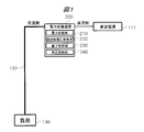
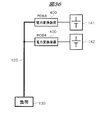
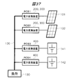
- FIG. 1 is a diagram illustrating an example of a system using the power conversion device according to the present embodiment.
- a DC power source 111 is connected to the DC side, and an AC power line 120 is connected to the AC side.
- the power conversion device 200 converts DC power input from the DC power supply 111 into AC power and outputs the AC power to the AC power line 120.
- a power conditioning system PCS which is a kind of power conversion device or various devices having a function of converting DC power into AC power is used.
- the load 130 is driven by receiving supply of AC power converted by the power conversion apparatus 200.
- the power conversion device 200 includes a power conversion unit 210, a frequency voltage control unit 220, a droop control unit 230, and a correction control unit 240.
- FIG. 2 is a diagram illustrating an example of the configuration of the power conversion device 200 according to the present embodiment.
- the power conversion device 200 includes a power conversion unit 210, a voltage detection unit 214, a current detection unit 215, and an AC power control unit 250.
- the power conversion unit 210 converts the DC power input from the DC power source 111 into AC power and outputs the AC power to the AC power line 120.
- the AC power control unit 250 controls the output frequency and output voltage of AC power output from the power conversion unit 210.
- the power conversion unit 210 includes a semiconductor element 211, a reactor 212, and a transformer 213, and constitutes an inverter that converts DC power into AC power.
- the semiconductor element 211 performs pulse width modulation on the input DC power by a switching operation based on control by the frequency voltage control unit 220 described later.
- Reactor 212 removes harmonics from the power subjected to pulse width modulation in semiconductor element 211. Through these steps, the DC power is converted into three-phase AC power.
- the transformer 213 transforms the pulse width modulated AC voltage into a predetermined output voltage.
- the AC power subjected to power conversion is output to the AC power line 120.
- the output frequency of the output AC power is, for example, 50 Hz or 60 Hz.
- the output voltage of the alternating current power output is 100V, 200V, etc., for example.
- the voltage detector 214 detects the output voltage of AC power. Specifically, the voltage detection unit 214 detects the output voltage of AC power output to the AC power line 120.
- the current detection unit 215 detects the output current of AC power. Specifically, the current detection unit 215 detects the output current of the AC power output to the AC power line 120.
- the AC power control unit 250 outputs AC power at a rated frequency and a rated voltage, and then based on the output voltage detected by the voltage detection unit 214 and the output current detected by the current detection unit 215, the output frequency and output of the AC power. After the drooping control for reducing the voltage from the rated frequency and the rated voltage, respectively, the correction control for gradually correcting the output frequency and the output voltage to the rated frequency and the rated voltage is performed.
- the AC power control unit 250 includes a drooping control unit 230, a correction control unit 240, and a frequency voltage control unit 220.
- the droop control unit 230 derives the contribution active power and the contribution reactive power of the AC power based on the output voltage and the output current, and based on the frequency droop rate and the contribution active power defined by the frequency reduction amount per active power, Deriving the frequency droop amount that lowers the output frequency from the rated frequency, and deriving the voltage droop amount that lowers the output voltage from the rated voltage based on the voltage droop rate specified by the voltage drop amount per reactive power and the contribution reactive power To do.
- the drooping control unit 230 includes a power calculation unit 231 that derives a contribution active power and a contribution reactive power of AC power based on an output voltage and an output current, and the contribution effective power and frequency derived by the power calculation unit 231.
- the frequency droop amount is derived by integrating the droop rate
- the voltage droop amount is derived by integrating the contribution reactive power derived by the power calculation unit 231 and the voltage droop rate.
- the power calculation unit 231 derives the contribution effective power by calculating the magnitude of the inner product of the output voltage detected by the voltage detection unit 214 and the output current detected by the current detection unit 215, for example.
- the power calculation unit 231 derives the contribution reactive power by calculating the magnitude of the outer product of the output voltage detected by the voltage detection unit 214 and the output current detected by the current detection unit 215, for example.
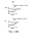
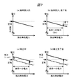
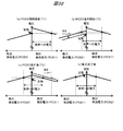
- FIG. 3 is a diagram for explaining the drooping characteristics.
- the drooping control for example, assuming that a plurality of power conversion devices 200 are connected to the AC power line 120 and parallel operation of outputting AC power from the plurality of power conversion devices 200 is performed, each power conversion device 200 is controlled. This is a control that is implemented to ensure fair sharing.
- FIG. 3A is a diagram showing a change in frequency with respect to active power.
- the frequency droop rate is the amount of decrease in frequency per active power, and is defined by the slope of the straight line shown in FIG.
- the frequency droop rate is set, for example, such that the amount of decrease in frequency (frequency droop rate) falls within a range that is allowed for the maximum effective power of the power conversion device 200.
- FIG. 3B is a diagram showing a change in voltage with respect to reactive power.
- the voltage droop rate is the amount of decrease in voltage per reactive power, and is defined by the slope of the straight line shown in FIG.
- the voltage droop rate is set, for example, such that the amount of voltage decrease (voltage droop rate) falls within a range that is allowed for the maximum reactive power of the power converter 200.
- Each unit and each function constituting the drooping control unit 230 may be configured by hardware or software.
- the droop control unit 230 includes a CPU (or a dedicated processor) (not shown), and the CPU stores a program stored in a memory or the like (not shown) To implement each unit and each function.
- the correction control unit 240 sets a frequency target value that defines the output frequency in the process of gradually correcting the output frequency reduced by the drooping control to the rated frequency based on the frequency correction value, and the droop control based on the voltage correction value
- the voltage target value that defines the output voltage in the process of gradually correcting the output voltage reduced by the above to the rated voltage is set.
- the correction control unit 240 will be described in detail.
- the correction control unit 240 stores the output status monitoring unit 241 that monitors the contribution active power and contribution reactive power derived by the power calculation unit 231, and the preset rated frequency, rated voltage, frequency droop rate, and voltage droop rate.
- a data storage unit 242 and a command value correction unit 243 are provided.
- Various data such as the rated frequency, the rated voltage, the frequency droop rate, and the voltage droop rate stored in the data storage unit 242 are input via the operation panel 290, for example.
- the operation panel 290 accepts input of various data such as a rated frequency, rated voltage, frequency droop rate, and voltage droop rate, and outputs the input various data to the data storage unit 242.
- the data storage unit 242 stores various data output from the operation panel.
- the operation panel 290 includes a display unit (not shown), and is configured to display various data such as the contribution active power and the contribution reactive power monitored by the output status monitoring unit 241 on the display unit.
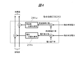
- FIG. 4 is a diagram illustrating an example of a configuration of a command value correction unit in the correction control unit.
- the command value correction unit 243 includes a frequency primary delay element (frequency delay element) 244 ⁇ and a voltage primary delay element (voltage delay element) 244v.
- the command value correction unit 243 integrates the contribution active power monitored by the output status monitoring unit 241 and the frequency droop rate stored in the data storage unit 242 to derive a frequency correction value, and the frequency correction value is delayed by the first order of the frequency.
- a frequency target that defines the output frequency in the process of gradually correcting the output frequency up to the rated frequency using the value obtained by adding the rated frequency to the frequency gradual correction value that is input to the element 244 ⁇ and output from the frequency primary delay element 244 ⁇ .
- the first-order lag element is used as a method of gradually changing the correction value, but a second-order lag element or more may be used for the same purpose.
- the command value correction unit 243 integrates the contribution reactive power monitored by the output status monitoring unit 241 and the voltage droop rate stored in the data storage unit 242 to derive a voltage correction value, and the voltage correction value is temporarily delayed by the voltage.
- a voltage target that regulates the output voltage in the process of gradually correcting the output voltage to the rated voltage using the value obtained by adding the rated voltage to the voltage gradually corrected value output from the voltage primary delay element 244v and input to the element 244v Set as a value.
- the frequency temporary delay element 244 ⁇ and the voltage first-order delay element 244v are used to cause the correction control by the correction control unit 240 to be performed gradually, that is, gradually.
- the frequency temporary delay element 244 ⁇ and the voltage first-order delay element 244v are constituted by, for example, a low-pass filter constituted by a resistor and a capacitor, a digital filter having the same function, or the like.
- the correction control is performed without passing through the frequency temporary delay element 244 ⁇ and the voltage primary delay element 244v, the correction control is performed, for example, in the time of several tens of us to 100 us.
- the correction control is performed through the frequency temporary delay element 244 ⁇ and the voltage primary delay element 244v, the correction control is performed in a time of several ms to several hundred ms, for example. Therefore, the correction control is performed over a considerably longer time than when the frequency temporary delay element 244 ⁇ and the voltage primary delay element 244v are not passed. Thereby, the correction control can be performed while suppressing fluctuations in the contribution active power and the contribution reactive power before and after the correction control.
- Each unit and each function constituting the correction control unit 240 may be configured by hardware or software.
- the correction control unit 240 includes a CPU (or a dedicated processor) (not shown), and the CPU stores a program stored in a memory or the like (not shown). To implement each unit and each function.
- correction control unit 240 may be implemented using, for example, a programmable logic controller (Programmable Logic Controller: hereinafter referred to as “PLC”) mounted in the power conversion device 200.
- PLC programmable logic controller
- the frequency voltage control unit 220 performs droop control based on the frequency droop amount and voltage droop amount calculated by the droop control unit 230, and after droop control, sets the frequency target value and voltage target value set by the correction control unit 240. Based on this, correction control is performed to gradually correct the output frequency and output voltage to the rated frequency and rated voltage.
- the frequency voltage control unit 220 includes a feedback control unit 221.
- the frequency voltage control unit 220 inputs the rated frequency and the rated voltage stored in the data storage unit 242 to the feedback control unit 221 as a frequency command value and a voltage command value, and the feedback control unit 221 inputs the frequency command value and Based on the voltage command value, AC power is output at the rated frequency and rated voltage.
- the frequency voltage control unit 220 inputs a value obtained by adding the rated frequency stored in the data storage unit 242 to the frequency droop amount derived in the droop control unit 230 as a frequency command value to the feedback control unit 221. Then, a value obtained by adding the rated voltage stored in the data storage unit 242 to the voltage droop amount derived in the droop control unit 230 is input to the feedback control unit 221 as a voltage command value, and the feedback control unit 221 The drooping control is performed based on the input frequency command value and voltage command value.
- the frequency voltage control unit 220 inputs the frequency target value and the voltage target value set by the command value correction unit 243 of the correction control unit 240 to the feedback control unit 221 as the frequency command value and the voltage command value, and the feedback control unit 221 Based on the input frequency command value and voltage command value, correction control is executed to gradually correct the output frequency and output voltage to the rated frequency and rated voltage.
- the feedback control unit 221 is connected to the voltage detection unit 214 and monitors the output voltage detected by the voltage detection unit 214.
- the feedback control unit 221 controls the pulse modulation signal based on the monitored output voltage so that the output voltage becomes a predetermined voltage.
- the feedback control unit 221 is connected to the current detection unit 215 and monitors the output voltage detected by the current detection unit 215.
- the feedback control unit 221 controls the pulse modulation signal based on the monitored output current so that the output voltage becomes a predetermined voltage. Since the output voltage decreases due to the current flowing through the reactor 212, the feedback control unit 221 compensates for the decreased amount according to the information from the current detection unit 215. Therefore, the feedback control unit 221 performs feedback control on the output voltage and output current. Thereby, the contribution active power and contribution reactive power of alternating current power are output stably.
- Each unit and each function constituting the frequency voltage control unit 220 may be configured by hardware or software.
- the frequency voltage control unit 220 includes a CPU (or a dedicated processor) (not shown), and the CPU is stored in a memory or the like (not shown).
- Each unit and each function is realized by executing the program.
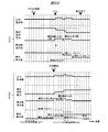
- FIG. 5 is a diagram showing a flowchart relating to frequency control and voltage control in the present embodiment.
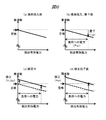
- FIG. 6 is a diagram showing drooping characteristics related to frequency control in the present embodiment.
- FIG. 7 is a diagram showing the drooping characteristics relating to the voltage control in the present embodiment.
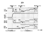
- FIG. 8 is a diagram showing a timing chart relating to frequency control in the present embodiment.
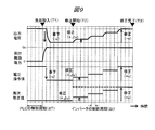
- FIG. 9 is a diagram illustrating a timing chart relating to voltage control in the present embodiment.
- control cycle of the power conversion unit (inverter) 210 is ⁇ t
- control cycle ⁇ T of the correction control unit (PLC) is 4 ⁇ t
- time constant of the frequency primary delay element 244 ⁇ and the voltage primary delay element 244v is 4 ⁇ T.
- the power conversion device 200 performs a rated output step S10, a frequency droop control step S20, a frequency correction control step S25, a voltage droop control step S30, and a voltage correction control step S35. Controls the output frequency and output voltage of AC power.
- a rated output step S10 Every time the sequence is activated, the rated output step S10 is executed every time, and the drooping steps S20 and S30 are executed by being thinned out at a certain rate. In other words, when thinning out by N, nothing is done in N-1 calls, but the process contents are executed for the first time in the Nth time.
- correction steps S25 and S35 are also thinned out and executed at a certain rate. Further, these steps do not need to be a series of sequences, and may be individually called from a management sequence such as a multitasking OS. Even in this case, it is important that the frequency of calling each process is different for each process. In the description of this example, it is assumed that they are incorporated in a series of sequences, the rated output process S10 and the drooping processes S20 and S30 are executed at the same timing, and the correction processes S25 and S35 are thinned out to some extent. Is assumed to be executed.
- the command value correction unit 243 reads the rated frequency and rated voltage stored in the data storage unit 242. At this time, since the correction control is not performed, both the frequency and voltage correction values are “0”. Therefore, the command value correction unit 243 sets the frequency target value and the voltage target value to the rated frequency and the rated voltage.
- the correction control unit 240 outputs the rated frequency and the rated voltage as the frequency target value and the voltage target value to the frequency voltage control unit 220.
- the frequency voltage control unit 220 sets the frequency command value and the voltage command value to the rated frequency and the rated voltage.
- the frequency voltage control unit 220 inputs the rated frequency and the rated voltage set as the frequency command value and the voltage command value to the feedback control unit 221.
- the feedback control unit 221 outputs AC power at a rated frequency and a rated voltage based on the input frequency command value and voltage command value.
- the power conversion unit (inverter) 210 passes an electric current through the load and maintains an AC voltage during the control period ⁇ t. Then, the power conversion device 200 outputs P ⁇ as the contribution active power as illustrated in FIG. 8. Moreover, the power converter device 200 outputs Qv as contribution reactive power, as shown in FIG.
- the drooping control unit 230 performs drooping control on the frequency and voltage. After performing the drooping control, the correction control is performed on the frequency and voltage. In the drooping control and the correction control, the control for the frequency and the voltage is performed in parallel.
- the drooping control and the correction control for the frequency are described, and then the drooping control and the correction control for the voltage are described. To do.
- the frequency drooping control step S20 will be described.
- the power conversion device 200 performs drooping control to lower the output frequency from the rated frequency, as shown in FIGS. 6B and 8.
- the droop control unit 230 derives the AC power contribution active power (P ⁇ ) based on the output voltage and the output current, and the frequency droop rate and the contribution active power defined by the frequency reduction amount per active power. Based on (P ⁇ ), a frequency droop amount ( ⁇ ) for deriving the output frequency from the rated frequency is derived.
- the power calculation unit 231 derives AC power contribution effective power (P ⁇ ) based on the output voltage detected by the voltage detection unit 214 and the output current detected by the current detection unit 215.
- the droop control unit 230 reads the frequency droop rate stored in the data storage unit 242, and integrates the contribution active power (P ⁇ ) derived by the power calculation unit 231 and the frequency droop rate read from the data storage unit 242.
- the amount of frequency droop ( ⁇ ) is derived.
- the droop control unit 230 outputs the frequency droop amount ( ⁇ ) derived as described above to the frequency voltage control unit 220.
- the correction control unit 240 outputs the rated frequency as the frequency target value to the frequency voltage control unit 220.
- the frequency voltage control unit 220 adds a value obtained by adding the rated frequency input from the correction control unit 240 to the frequency droop amount ( ⁇ ) input from the droop control unit 230 as a frequency command value as a feedback control unit 221.
- the feedback control unit 221 performs drooping control that reduces the frequency by a frequency drooping amount ( ⁇ ) from the rating based on the input frequency command value. As shown in FIG. 8, the frequency voltage controller 220 performs the drooping control in the period of the inverter control cycle ⁇ t.
- the frequency correction control step S25 After performing the drooping control, the power conversion device 200 performs correction control for gradually correcting the frequency to the rated frequency from time T2 in FIG. Specifically, the correction control unit 240 sets the frequency droop amount ( ⁇ ) as a frequency correction value (+ ⁇ ) for correcting the output frequency to the rated frequency, and sets the output frequency to the rated frequency based on the frequency correction value (+ ⁇ ). The frequency target value is set based on the gradually corrected value (+ ⁇ ) that defines the output frequency in the process of gradually correcting until.
- the command value correction unit 243 derives a frequency correction value (+ ⁇ ) by integrating the contribution active power monitored by the output status monitoring unit 241 and the frequency droop rate read from the data storage unit 242, and the frequency correction value (+ ⁇ ) is input to the frequency primary delay element 244 ⁇ .
- the frequency primary delay element 244 ⁇ outputs a gradual frequency correction value (+ ⁇ ) based on the input frequency correction value.
- the command value correction unit 243 adds the rated frequency read from the data storage unit 242 to the frequency gradual correction value (+ ⁇ ) output from the frequency primary delay element 244 ⁇ , and sets the output frequency to the rated frequency.
- the output frequency in the process of gradual correction is set as a frequency target value that defines the output frequency.
- the command value correction unit 243 outputs the frequency target value set here to the frequency voltage control unit 220.
- the frequency voltage control unit 220 performs output frequency correction control using the frequency target value input from the command value correction unit 243 as the frequency command value. At this time, as shown in FIG. 6C and FIG. 8, the output frequency increases by ⁇ in the control period ⁇ t of the first inverter from the start of the correction control.
- the frequency primary delay element 244 ⁇ outputs (+ 2 ⁇ ) as a gradually corrected value. Based on this, the frequency voltage control unit 220 further performs correction control of the frequency for ⁇ . By repeating such correction control, as shown in FIG. 6D and FIG. 8, the feedback control unit 221 performs correction control for + ⁇ for the output frequency.
- the frequency voltage control unit 220 ends the correction control. As a result, the frequency voltage controller 220 gradually corrects the output frequency to the rated frequency. That is, by passing the first-order frequency delay element 244 ⁇ , the feedback control unit 221 gradually and slowly controls the output frequency to the rated frequency.
- FIG. 8 as an example of the correction control, the case where correction is performed in four stages has been described. However, the present invention is not limited to such a case. For example, the correction control may be performed through more stages. .
- the voltage droop control step S30 will be described. As described above, the voltage droop control step S30 is performed in parallel with the frequency droop control step S20. When the load 130 is turned on and AC power is output, the power conversion device 200 performs drooping control to reduce the output voltage from the rated voltage, as shown in FIGS. 7B and 9.
- the droop control unit 230 derives the AC reactive power reactive power (Qv) based on the output voltage and output current, and the voltage droop rate and the power reactive power defined by the amount of voltage drop per reactive power. Based on (Qv), a voltage droop amount ( ⁇ v) for deriving the output voltage from the rated voltage is derived.
- the power calculator 231 derives the AC reactive power reactive power (Qv) based on the output voltage detected by the voltage detector 214 and the output current detected by the current detector 215.
- the droop control unit 230 reads the voltage droop rate stored in the data storage unit 242 and integrates the contribution reactive power (Qv) derived by the power calculation unit 231 and the voltage droop rate read from the data storage unit 242.
- the voltage droop amount ( ⁇ v) is derived.
- the droop control unit 230 outputs the voltage droop amount ( ⁇ v) derived in this way to the frequency voltage control unit 220.
- the correction control unit 240 outputs the rated voltage as the voltage target value to the frequency voltage control unit 220.
- the frequency voltage controller 220 adds a value obtained by adding the rated voltage input from the correction controller 240 to the voltage droop amount ( ⁇ v) input from the droop controller 230 as a voltage command value as a feedback controller 221. To enter.
- the feedback control unit 221 performs drooping control that reduces the voltage from the rating by a voltage drooping amount ( ⁇ v) based on the input voltage command value.
- the frequency voltage controller 220 reduces the output voltage by the voltage droop amount ( ⁇ v) during the inverter control period ⁇ t.
- the voltage correction control step S35 is performed in parallel with the frequency droop control step S30.
- the power conversion device 200 After performing the drooping control, the power conversion device 200 performs correction control for gradually correcting the voltage to the rated voltage from time T2 in FIG.
- the correction control unit 240 sets the voltage droop amount ( ⁇ v) as a voltage correction value (+ v) for correcting the output voltage to the rated voltage, and converts the output voltage to the rated voltage based on the voltage correction value (+ v).
- the voltage target value is set based on the gradually corrected value (+ ⁇ v) that defines the output voltage in the process of gradually correcting until.
- the command value correction unit 243 derives a voltage correction value (+ v) by integrating the contribution reactive power monitored by the output status monitoring unit 241 and the voltage droop rate read from the data storage unit 242, and the voltage correction value (+ V) is input to the voltage first-order lag element 244 ⁇ .
- the voltage primary delay element 244v outputs a voltage gradual correction value (+ ⁇ v) based on the input voltage correction value.
- the command value correction unit 243 adds the rated voltage read from the data storage unit 242 to the voltage gradual correction value (+ ⁇ v) output from the voltage primary delay element 244v, and sets the output voltage to the rated voltage.
- the output voltage in the process of gradual correction is set as a voltage target value that defines the output voltage.
- the command value correction unit 243 outputs the voltage target value set here to the frequency voltage control unit 220.
- the frequency voltage control unit 220 performs output voltage correction control using the voltage target value input from the command value correction unit 243 as a voltage command value. At this time, as shown in FIG. 7C and FIG. 9, the output voltage increases by ⁇ in the control period ⁇ t of the first inverter from the start of the correction control.
- the voltage primary delay element 244v outputs (+ 2 ⁇ v) as a gradually corrected value.
- the frequency voltage control unit 220 further performs correction control of the voltage for ⁇ v.
- the feedback control unit 221 performs correction control for + ⁇ for the output voltage.
- the frequency voltage control unit 220 ends the correction control.
- the frequency voltage controller 220 gradually corrects the output voltage to the rated voltage. That is, by passing the voltage first-order lag element 244v, the feedback control unit 221 gradually and slowly corrects the output voltage to the rated voltage.
- FIG. 9 as an example of the correction control, the case where the correction is performed in four stages has been described.
- the present invention is not limited to such a case.
- the correction control may be performed through more stages. .
- the power conversion device 200 controls the output frequency and output voltage of the AC power to be output.
- the drooping control and the correction control are performed by separate mechanisms (the drooping control unit 230 and the correction control unit 240).
- the inverter control cycle ⁇ t is sufficiently shorter than the PLC control cycle ⁇ T.
- these cycles may be substantially equal.
- the frequency voltage control unit 220 outputs the AC power at the rated frequency and the rated voltage, and then stores the rating stored in the data storage unit 242 in the frequency droop amount derived by the droop control unit 230.
- a value obtained by adding the frequencies is input to the feedback control unit 221 as a frequency command value.
- the frequency voltage control unit 220 inputs a value obtained by adding the rated voltage stored in the data storage unit 242 to the voltage droop amount derived by the droop control unit 230 as a voltage command value to the feedback control unit 221.
- the feedback control unit 221 performs drooping control based on the input frequency command value and voltage command value.
- the frequency voltage control unit 220 inputs the frequency target value and the voltage target value set by the command value correction unit 243 of the correction control unit 240 to the feedback control unit 221 as the frequency command value and the voltage command value, and the feedback control unit 221.
- the correction control for gradually correcting the output frequency and the output voltage to the rated frequency and the rated voltage is performed.
- the frequency first-order lag element 244 ⁇ starts the correction control (T2), and then gradually increases the frequency correction value by + ⁇ for each control period ⁇ T of the PLC. increase.
- the command value correction unit 243 is set so as to gradually increase the frequency target value, so that the feedback control unit 221 can gradually correct the output frequency to the rated frequency using the frequency target value as the frequency command value. Thereby, the contribution active power can be maintained substantially equal before and after the correction control.
- the voltage first-order lag element 244v starts the correction control (T2), and then gradually increases the voltage correction value by + ⁇ v every PLC control period ⁇ T. increase.
- the command value correcting unit 243 is set so as to gradually increase the voltage target value, so that the feedback control unit 221 can gradually correct the output frequency to the rated frequency using the voltage target value as the voltage command value. Thereby, the contribution reactive power can be maintained substantially the same before and after the correction control.
- the feedback control unit 221 can monitor the output power detected by the voltage detection unit 214 and the output current detected by the current detection unit 215. Thereby, the feedback control unit 221 can feedback control the output voltage and the output current. Thereby, the contribution active power and contribution reactive power of alternating current power can be output stably. In addition, this makes it possible to stably supply AC power to the load 130.
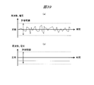
- FIG. 38 is a diagram illustrating a timing chart relating to frequency and voltage control in the power conversion device studied by the present inventors.
- FIG. 39 is a diagram showing the characteristics of the output frequency and the output voltage in the power conversion device studied by the present inventors.
- FIG. 38 shows a case where the correction control is not performed after the drooping control is performed. Since the correction control is not performed, as shown in FIG. 38, AC power is supplied while the output frequency is reduced from the rated frequency by a frequency droop amount ( ⁇ 1). Further, AC power is supplied while the output voltage is lowered from the rated voltage by a voltage droop amount ( ⁇ v1).
- the output frequency and output power fluctuate around the rating as shown in FIG. 39 (a), but when the system is not connected, the output frequency and As shown in FIG. 39B, the output voltage continues to be lowered from the rating by a frequency droop amount (for example, ⁇ 1) and a voltage droop amount (for example, ⁇ v1).
- a frequency droop amount for example, ⁇ 1
- a voltage droop amount for example, ⁇ v1
- Embodiment 2 demonstrates the case where alternating current power is output with respect to the load 130 by the some power converter device 200 (PCS1, PCS2).
- FIG. 10 is a diagram illustrating an example of a system according to the present embodiment.
- a DC power source 121 is connected to the DC side, and an AC power line 120 is connected to the AC side.
- the power conversion device 200 (PCS1) converts the DC power input from the DC power supply 121 into AC power and outputs the AC power to the AC power line 120.
- a DC power source 122 is connected to the DC side, and an AC power line 120 is connected to the AC side.
- the power converter 200 (PCS2) converts DC power input from the DC power supply 122 into AC power and outputs the AC power to the AC power line 120.
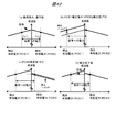
- FIG. 11 is a diagram showing a flowchart relating to frequency control and voltage control in the present embodiment.
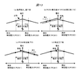
- FIG. 12 is a diagram illustrating drooping characteristics related to frequency control in the present embodiment.
- FIG. 13 is a diagram illustrating drooping characteristics related to voltage control in the present embodiment.
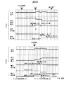
- FIG. 14 is a diagram showing a timing chart relating to frequency control in the present embodiment.
- FIG. 15 is a diagram illustrating a timing chart relating to voltage control in the present embodiment.
- each power conversion device 200 includes a rated output step S110, a frequency droop control step S120, a frequency correction control step S125, a voltage droop control step S130, and a voltage correction control step S135.
- the output frequency and output voltage of the AC power are controlled. Note that the above-described steps S110 to S135 are performed in parallel in each power conversion device 200. For this reason, when explaining each process, operation in each power converter 200 (PCS1, PCS2) is explained together.
- control cycle of the power conversion unit (inverter) 210 is ⁇ t
- control cycle ⁇ T of the correction control unit (PLC) is 4 ⁇ t
- time constant of the frequency primary delay element 244 ⁇ and the voltage primary delay element 244v is 4 ⁇ T.
- each power conversion device 200 When the load 130 is dropped at time T1, each power conversion device 200 (PCS1, PCS2) outputs AC power supplied to the load 130 almost simultaneously.
- the AC power output from each power conversion device 200 is assigned according to each output impedance.
- the power conversion unit (inverter) 210 of each power conversion device 200 (PCS1, PCS2) allows a current to flow through the load and maintains an AC voltage during the control period ⁇ t. Then, the power conversion device 200 (PCS1) outputs P ⁇ 1 as the contribution active power as shown in FIG. Moreover, the power converter device 200 (PCS1) outputs Qv1 as contribution reactive power, as shown in FIG.
- the power conversion device 200 (PCS2) outputs P ⁇ 2 as the contribution active power as shown in FIG. Moreover, the power converter device 200 (PCS2) outputs Qv2 as contribution reactive power, as shown in FIG.
- the active power supplied to the load 130 is P ⁇ 1 + P ⁇ 2
- the reactive power supplied to the load 130 is Qv1 + Qv2.
- the drooping control unit 230 of each power converter 200 (PCS1, PCS2) performs drooping control on the frequency and voltage. After performing the drooping control, the correction control is performed on the frequency and voltage. In the drooping control and the correction control, the control for the frequency and the voltage is performed in parallel.
- the drooping control and the correction control for the frequency are described, and then the drooping control and the correction control for the voltage are described. To do.
- the frequency drooping control step S120 will be described.
- the power converter 200 (PCS1, PCS2) performs drooping control to lower the output frequency from the rated frequency, as shown in FIGS. To do.
- the power converter 200 (PCS1) has earlier inverter control timing than the power converter 200 (PCS2), so the power converter 200 (PCS1) starts the droop control first. To do.
- the drooping control unit 230 of the power conversion device 200 derives the frequency drooping amount ( ⁇ 1) based on the contributed active power (P ⁇ 1).
- the feedback control unit 221 of the frequency voltage control unit 220 reduces the output frequency from the rating by the frequency droop amount ( ⁇ 1) using the value obtained by adding the rated frequency to the frequency droop amount ( ⁇ 1) as the frequency command value.
- Implement drooping control As a result, the frequency voltage controller 220 reduces the output frequency by the amount of frequency droop ( ⁇ 1) during the inverter control period ⁇ t, as shown in FIG.
- the feedback control unit 221 performs the drooping control in the period of the inverter control cycle ⁇ t.
- the power conversion device 200 starts the drooping control after the drooping control by the power conversion device 200 (PCS1) is started and before the drooping control is ended.
- the drooping control unit 230 of the power conversion device 200 derives the frequency drooping amount ( ⁇ 2) based on the contributed active power (P ⁇ 2).
- the feedback control unit 221 of the frequency voltage control unit 220 reduces the output frequency from the rating by the frequency droop amount ( ⁇ 2) using the value obtained by adding the rated frequency to the frequency droop amount ( ⁇ 2) as the frequency command value.
- Implement drooping control As a result, the frequency voltage control unit 220 reduces the output frequency by the frequency droop amount ( ⁇ 2) during the inverter control period ⁇ t.
- the frequency drooping amount in the power conversion devices 200 is substantially the same in each power conversion device 200 (PCS1, PCS2).
- PCS1, PCS2 since the timing at which the droop control is performed differs between the power conversion devices 200 (PCS1, PCS2), there is a deviation in the reflection of the frequency droop amount according to the contribution active power. Due to this deviation, a current flows between the power conversion devices 200 (PCS1, PCS2) in the form of a cross current.
- the frequency correction control process S125 will be described.
- the power conversion device 200 (PCS1) After performing the drooping control, the power conversion device 200 (PCS1) performs correction control for gradually correcting the frequency to the rated frequency from time T2 in FIG. However, as shown in FIG. 14, the power converter 200 (PCS1) has an earlier inverter control timing than the power converter 200 (PCS2), so the power converter 200 (PCS1) first corrects the output frequency. Start control.
- the command value correction unit 243 of the power conversion device 200 integrates the contribution active power monitored by the output status monitoring unit 241 and the frequency droop rate read from the data storage unit 242, thereby correcting the frequency correction value (+ ⁇ 1). ) Is derived, and the frequency correction value (+ ⁇ 1) is input to the frequency primary delay element 244 ⁇ .
- the frequency primary delay element 244 ⁇ outputs a gradual frequency correction value (+ ⁇ 1) based on the input frequency correction value.
- the command value correction unit 243 adds the rated frequency read from the data storage unit 242 to the frequency gradual correction value (+ ⁇ 1) output from the frequency primary delay element 244 ⁇ , and sets the output frequency to the rated frequency.
- the output frequency in the process of gradual correction is set as a frequency target value that defines the output frequency.
- the command value correction unit 243 outputs the frequency target value set here to the frequency voltage control unit 220.
- the frequency voltage control unit 220 performs output frequency correction control using the frequency target value input from the command value correction unit 243 as a frequency command value.
- the output frequency of the power converter 200 (PCS1) is increased by the correction control. For this reason, as shown in FIG.12 (b), the active power which the power converter device 200 (PCS2) contributes reduces, and the active power which the power converter device 200 (PCS1) contributes increases.
- the power conversion device 200 (PCS1), at time T3, the power conversion device 200 (PCS2) also starts the correction control of the output frequency.
- the command value correction unit 243 of the power conversion device 200 integrates the contribution active power monitored by the output status monitoring unit 241 and the frequency droop rate read from the data storage unit 242, thereby correcting the frequency correction value (+ ⁇ 2).
- the frequency correction value (+ ⁇ 2) is input to the frequency primary delay element 244 ⁇ .
- the frequency primary delay element 244 ⁇ outputs a gradual correction value (+ ⁇ 2) based on the input frequency correction value.
- the command value correction unit 243 adds the rated frequency read from the data storage unit 242 to the frequency gradual correction value (+ ⁇ 2) output from the frequency primary delay element 244 ⁇ , and sets the output frequency to the rated frequency.
- the output frequency in the process of gradual correction is set as a frequency target value that defines the output frequency.
- the command value correction unit 243 outputs the frequency target value set here to the frequency voltage control unit 220. As illustrated in FIG. 12C, the frequency voltage control unit 220 performs output frequency correction control using the frequency target value input from the command value correction unit 243 as a frequency command value.
- the output frequency of the power converter 200 (PCS2) is increased by the correction control. For this reason, as shown in FIG.12 (c), the active power which the power converter device 200 (PCS1) contributes reduces, and the active power which the power converter device 200 (PCS2) contributes increases.
- each power conversion device 200 (PCS1, PCS2) corrects the output frequency to the rated frequency as shown in FIG. 12 (d) and FIG.
- the droop control unit 230 of the power conversion device 200 derives the voltage droop amount ( ⁇ v1) based on the contribution reactive power (Qv1).
- the feedback control unit 221 of the frequency voltage control unit 220 reduces the output voltage from the rating by the voltage droop amount ( ⁇ v1) using the value obtained by adding the rated voltage to the voltage droop amount ( ⁇ v1) as the voltage command value.
- the frequency voltage controller 220 reduces the output voltage by the amount of voltage droop ( ⁇ v1) during the period of the control period ⁇ t of the inverter, as shown in FIG.
- the feedback control unit 221 performs the drooping control in the period of the inverter control cycle ⁇ t.
- the power conversion device 200 starts the drooping control after the drooping control by the power conversion device 200 (PCS1) starts and before the drooping control ends.
- the droop control unit 230 of the power conversion device 200 derives the voltage droop amount ( ⁇ v2) based on the contribution reactive power (Qv2).
- the feedback control unit 221 of the frequency voltage control unit 220 reduces the output voltage from the rating by the voltage droop amount ( ⁇ v2) using the value obtained by adding the rated voltage to the voltage droop amount ( ⁇ v2) as the voltage command value.
- Implement drooping control As a result, the frequency voltage controller 220 reduces the output voltage by the voltage droop amount ( ⁇ v2) during the inverter control period ⁇ t.
- the amount of voltage droop in the power conversion devices 200 is substantially the same in each power conversion device 200 (PCS1, PCS2).
- PCS1, PCS2 since the timing at which the drooping control is performed differs between the power conversion devices 200 (PCS1, PCS2), there is a deviation in the reflection of the voltage droop according to the contribution reactive power. Due to this deviation, a current flows between the power conversion devices 200 (PCS1, PCS2) in the form of a cross current.
- Voltage correction control step S135 Next, the voltage correction control process S135 will be described.
- the power conversion device 200 (PCS1) After performing the drooping control, the power conversion device 200 (PCS1) performs correction control for gradually correcting the voltage to the rated voltage from time T2 in FIG. However, as shown in FIG. 15, the power converter 200 (PCS1) has an inverter control timing earlier than that of the power converter 200 (PCS2), so the power converter 200 (PCS1) corrects the output voltage first. Start control.
- the command value correction unit 243 of the power conversion device 200 integrates the contribution active power monitored by the output status monitoring unit 241 and the voltage droop rate read from the data storage unit 242, thereby correcting the voltage correction value (+ v1).
- the voltage correction value (+ v1) is input to the voltage first-order lag element 244v.
- the voltage primary delay element 244v outputs a voltage gradual correction value (+ ⁇ v1) based on the input voltage correction value.
- the command value correction unit 243 adds the rated voltage read from the data storage unit 242 to the voltage gradual correction value (+ ⁇ v1) output from the voltage primary delay element 244v, and outputs the output voltage up to the rated voltage.
- the output voltage in the process of gradual correction is set as a voltage target value that defines the output voltage.
- the command value correction unit 243 outputs the voltage target value set here to the frequency voltage control unit 220.
- the frequency voltage control unit 220 performs output voltage correction control using the voltage target value input from the command value correction unit 243 as a voltage command value.
- the output voltage of the power converter 200 (PCS1) is increased by the correction control. For this reason, as shown in FIG.13 (b), the reactive power which the power converter device 200 (PCS2) contributes reduces, and the reactive power which the power converter device 200 (PCS1) contributes increases.
- the power conversion device 200 (PCS1), at time T3, the power conversion device 200 (PCS2) also starts the correction control of the output voltage.
- the command value correction unit 243 of the power conversion device 200 integrates the contribution active power monitored by the output status monitoring unit 241 and the voltage droop rate read from the data storage unit 242, thereby correcting the voltage correction value (+ v2).
- the voltage correction value (+ v2) is input to the voltage first-order lag element 244v.
- the voltage primary delay element 244v outputs a voltage gradual correction value (+ ⁇ v2) based on the input voltage correction value.
- the command value correction unit 243 adds the rated voltage read from the data storage unit 242 to the voltage gradual correction value (+ ⁇ v2) output from the voltage primary delay element 244v, and sets the output voltage to the rated voltage.
- the output voltage in the process of gradual correction is set as a voltage target value that defines the output voltage.
- the command value correction unit 243 outputs the voltage target value set here to the frequency voltage control unit 220. As illustrated in FIG. 13C, the frequency voltage control unit 220 performs output voltage correction control using the voltage target value input from the command value correction unit 243 as a voltage command value.
- the output voltage of the power converter 200 (PCS2) is increased by the correction control. For this reason, as shown in FIG.13 (c), the reactive power which the power converter device 200 (PCS1) contributes reduces, and the reactive power which the power converter device 200 (PCS2) contributes increases.
- each power conversion device 200 (PCS1, PCS2) corrects the output voltage to the rated voltage as shown in FIG. 13 (d) and FIG.
- the power conversion device 200 controls the output frequency and output voltage of the AC power to be output.
- the case where the two power conversion devices 200 (PCS1, PCS2) are operated in parallel has been described, but the present invention is not limited to this. For example, three or more power conversion devices 200 may be connected in parallel. Good.
- the correction control is gradually performed in each of the plurality of power conversion devices 200 (PCS1, PCS2).
- the correction control is performed.
- each power converter device 200 can share contribution active power and contribution reactive power fairly. Therefore, the frequency and voltage can be maintained at the ratings while utilizing the controllability to share the load fairly.
- the correction control is performed after the droop control, it is not necessary to reduce the droop amount in order to suppress deviation from the rating. As a result, it is possible to share information on the contributed power with the other power conversion devices 200 (PCS1, PCS2) without reducing the control accuracy required for load sharing.
- FIG. 40 is a diagram illustrating drooping characteristics of the output frequency and the output voltage in the power conversion device studied by the present inventors.
- FIG. 41 is a diagram illustrating a timing chart relating to frequency and voltage control in the power conversion device studied by the present inventors. Here, a case is shown in which the correction control is not performed after the drooping control is performed.
- both power converters PCS1, PCS2
- both power conversion devices PCS1, PCS2
- ⁇ v1 voltage droop amount
- both power conversion devices PCS1, PCS2
- both power converters PCS1, PCS2
- both power converters output AC power in a state where the output voltage is reduced from the rated voltage by a voltage droop amount ( ⁇ v1).
- the output frequency and the output voltage cannot be corrected to the rating while the drooping control is performed. For this reason, if it is going to implement droop control, suppressing drooping amount, the control precision required for load sharing will fall. Moreover, it may occur that it becomes difficult to share information on the contribution power with the other power conversion devices 200 (PCS1, PCS2).
- each power conversion device is corrected while cooperating by sharing the frequency correction value and the voltage correction value of all the power conversion devices related to the parallel operation. A case where control is performed will be described.
- FIG. 16 is a diagram illustrating an example of a configuration of the power conversion device according to the present embodiment.
- FIG. 17 is a diagram illustrating an example of a configuration of a command value correction unit in the correction control unit.
- FIG. 18 is a diagram illustrating an example of the configuration of the cooperative control unit in the correction control unit.
- the power conversion device 300 includes a power conversion unit 210, a voltage detection unit 214, a current detection unit 215, and an AC power control unit 350.
- the AC power control unit 350 includes a drooping control unit 230, a correction control unit 340, and a frequency voltage control unit 220.
- the correction control unit 340 includes an output status monitoring unit 241, a data storage unit 242, a command value correction unit 343, a cooperative control unit 345, and a network interface unit 346.
- the network interface unit 346 performs data transmission / reception with another power conversion device 300 related to parallel operation. Specifically, the network interface unit 346 is implemented with elements necessary for general network communication such as elements satisfying a network protocol used for communication with the plurality of power conversion devices 300 and arbitration of communication for each purpose. Yes.
- the network interface unit 346 receives an external frequency correction value and an external voltage correction value, which will be described later, of other power conversion devices 300 participating in the parallel operation. Specifically, the correction value entry control unit 361 described later inquires all the other power conversion devices 300 participating in the parallel operation via the network interface unit 346. All other power conversion devices 300 transmit the internal frequency correction value and the internal voltage correction value possessed by each power conversion device 300 as the external frequency correction value and the external voltage correction value. The network interface unit 346 receives the transmitted external frequency correction value and external voltage correction value of all other power conversion devices 300. The network interface unit 346 transmits the received external frequency correction value and external voltage correction value of the other power conversion device 300 to the cooperative control unit 345. Further, the network interface unit 346 transmits its internal frequency correction value and internal voltage correction value to the other power conversion device 300 as the external frequency correction value and the external voltage correction value.
- the cooperative control unit 345 performs correction control in cooperation with another power conversion device 300 related to parallel operation. As shown in FIG. 18, the cooperative control unit 345 includes a correction value entry control unit 361, an external frequency correction value storage unit 362 ⁇ , an external frequency correction value comparison unit 363 ⁇ , an external voltage correction value storage unit 362v, and an external voltage correction value comparison unit. 363v is provided.
- the correction value entry control unit 361 receives the input of the external frequency correction value and the external voltage correction value of the other power conversion device 300 transmitted from the network interface unit 346. Of the input external frequency correction value and external voltage correction value, the correction value entry control unit 361 outputs the external frequency correction value to the external frequency correction value storage unit 362 ⁇ and outputs the external voltage correction value to the external voltage correction value storage unit. To 362v.
- the external frequency correction value storage unit 362 ⁇ stores the input external frequency correction value.
- the external voltage correction value storage unit 362v stores the input external voltage correction value.
- the correction value entry control unit 361, the external frequency correction value storage unit 362 ⁇ , and the external voltage correction value storage unit 362v perform these operations for all the other power conversion devices 300 that participate in the parallel operation.
- the external frequency correction value comparison unit 363 ⁇ compares all external frequency correction values stored in the external frequency correction value storage unit 362 ⁇ , and outputs the maximum external frequency correction value to the command value correction unit 343 as the maximum external frequency correction value. To do. Specifically, the external frequency correction value comparison unit 363 ⁇ reads all external frequency correction values stored in the external frequency correction value storage unit 362 ⁇ , compares the external frequency correction values, and maximizes the maximum external frequency correction value. It is output to the command value correction unit 343 as an external frequency correction value.
- the external voltage correction value comparison unit 363v compares all external voltage correction values stored in the external voltage correction value storage unit 362v, and outputs the maximum external voltage correction value as the maximum external voltage correction value to the command value correction unit 343. To do. Specifically, the external voltage correction value comparison unit 363v reads all the external voltage correction values stored in the external voltage correction value storage unit 362v, compares the external voltage correction values, and maximizes the maximum external voltage correction value. The external voltage correction value is output to the command value correction unit 343.
- the command value correction unit 343 defines the output frequency and the output voltage in correction control. As shown in FIG. 17, the command value correction unit 343 includes a frequency correction value comparison unit 347 ⁇ , a voltage correction value comparison unit 347v, a frequency primary delay element 244 ⁇ , and a voltage primary delay element 244v.
- the command value correction unit 343 derives an internal frequency correction value by integrating the contribution active power monitored by the output status monitoring unit 241 and the frequency droop rate stored in the data storage unit 242.
- the derived internal frequency correction value is input to the frequency correction value comparison unit 347 ⁇ .
- the frequency correction value comparison unit 347 ⁇ receives the input of the maximum external frequency correction value output from the external frequency correction value comparison unit 363 ⁇ .
- the frequency correction value comparison unit 347 ⁇ compares the internal frequency correction value and the maximum external frequency correction value, and derives the larger one of the internal frequency correction value and the maximum external frequency correction value as the frequency correction value.
- the frequency correction value is input to the frequency primary delay element 244 ⁇ .
- the command value correction unit 343 defines the output frequency in the process of gradually correcting the output frequency to the rated frequency, by adding the rated frequency to the frequency gradual correction value output from the frequency primary delay element 244 ⁇ . Set as target value.
- the maximum frequency correction value among the frequency correction values in all the power conversion devices 300 participating in the parallel operation is used as the frequency correction value. That is, in all the power converters 300, the same frequency correction value is used in the correction control, so the correction control is performed in cooperation.
- the command value correction unit 343 derives an internal voltage correction value by integrating the contribution reactive power monitored by the output status monitoring unit 241 and the voltage droop rate stored in the data storage unit 242.
- the derived internal voltage correction value is input to the voltage correction value comparison unit 347v.
- the voltage correction value comparison unit 347v receives the input of the maximum external voltage correction value output from the external voltage correction value comparison unit 363v.
- the voltage correction value comparison unit 347v compares the internal voltage correction value and the maximum external voltage correction value, and derives the larger one of the internal voltage correction value and the maximum external voltage correction value as the voltage correction value.
- the voltage correction value is input to the voltage primary delay element 244v.
- the command value correction unit 343 defines a voltage obtained by adding the rated voltage to the voltage gradual correction value output from the voltage first-order lag element 244v, and the output voltage in the process of gradually correcting the output voltage to the rated voltage. Set as target value.
- the maximum voltage correction value among the voltage correction values in all the power conversion devices 300 participating in the parallel operation is used as the voltage correction value. That is, in all the power converters 300, the same voltage correction value is used in the correction control, so the correction control is performed in cooperation.
- Each unit and each function constituting the correction control unit 340 may be configured by hardware or software.
- the correction control unit 340 includes a CPU (or a dedicated processor) (not shown), and the CPU stores a program stored in a memory or the like (not shown). To implement each unit and each function.
- the correction control unit 340 may be mounted using, for example, a programmable logic controller (PLC) mounted on the power conversion device 300.
- PLC programmable logic controller
- the control cycle of the power conversion unit (inverter) 210 is ⁇ t
- the control cycle ⁇ T of the correction control unit (PLC) is 4 ⁇ t
- the time constant of the frequency primary delay element 244 ⁇ and the voltage primary delay element 244v is 4 ⁇ T.
- the inverter control cycle ⁇ t is the same, but the inverter control timing and the PLC control timing are different.
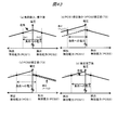
- FIG. 19 is a diagram showing a flowchart relating to frequency control and voltage control in the present embodiment.
- FIG. 20 is a diagram illustrating drooping characteristics related to frequency control when the time constant is large.
- FIG. 21 is a diagram illustrating drooping characteristics related to voltage control when the time constant is large.
- FIG. 22 is a diagram illustrating a timing chart related to frequency control when the time constant is large.
- FIG. 23 is a timing chart relating to voltage control when the time constant is large.
- the power conversion device 300 performs each of a rated output step S210, a frequency droop control step S220, a frequency correction control step S225, a voltage droop control step S230, and a voltage correction control step S235. Controls the output frequency and output voltage of AC power.
- the rated output step S210, the frequency droop control step S220, and the voltage droop control step S230 are controlled in the same manner as the rated output step S110, the frequency droop control step S120, and the voltage droop control step S130 in the second embodiment. Since it is implemented, the description is omitted here.
- the frequency correction control process S225 will be described.
- the frequency correction value comparison unit 347 ⁇ inputs the derived frequency correction value to the frequency primary delay element 244 ⁇ .
- the frequency primary delay element 244 ⁇ outputs a gradual correction value based on the input frequency correction value.
- the feedback control unit 221 performs frequency correction control based on the frequency gradual correction value. Thus, correction control is performed with the maximum value among the internal frequency correction values of all power conversion devices 300 (PCS1, PCS2) participating in parallel operation as the frequency correction value.
- the power conversion device 300 also derives the same frequency correction value as that of the power conversion device 300 (PCS1), and performs frequency correction control based on this in coordination.
- the frequency gradual correction value output by the frequency primary delay element 244 ⁇ is not immediately reflected in the frequency target value (frequency command value). Therefore, there is no significant imbalance in the effective contribution power between the power conversion device 300 (PCS1) and the power conversion device 300 (PCS2) due to the correction value.
- the frequency correction control in this case is almost the same as the frequency correction control in the frequency correction control step S125 in the second embodiment.
- the voltage correction control process S235 will be described.
- the voltage correction value comparison unit 347v inputs the derived voltage correction value to the voltage primary delay element 244v.
- the voltage primary delay element 244v outputs a voltage gradual correction value based on the input voltage correction value.
- the feedback control unit 221 performs voltage correction control based on the voltage gradual correction value.
- the correction control is performed with the maximum value among the internal voltage correction values of all the power conversion devices 300 (PCS1, PCS2) participating in the parallel operation as the voltage correction value.
- the power conversion device 300 also derives the same voltage correction value as that of the power conversion device 300 (PCS1), and performs voltage correction control based on this in coordination.
- the voltage gradual correction value output from the voltage primary delay element 244v is not immediately reflected in the voltage target value (voltage command value). Therefore, there is no large imbalance of the contribution reactive power between the power conversion device 300 (PCS1) and the power conversion device 300 (PCS2) due to the correction value.
- the voltage correction control in this case is almost the same as the voltage correction control in the voltage correction control step S135 in the above-described second embodiment, as shown in FIGS.
- FIG. 24 is a diagram illustrating drooping characteristics related to frequency control when the time constant is small.
- FIG. 25 is a diagram illustrating drooping characteristics related to voltage control when the time constant is small.
- FIG. 26 is a diagram illustrating a timing chart related to frequency control when the time constant is small.
- FIG. 27 is a diagram illustrating a timing chart relating to voltage control when the time constant is small.
- time constants of the frequency primary delay element 244 ⁇ and the voltage primary delay element 244v are assumed to be 2 ⁇ T as an example when the time constant is small.
- the frequency gradual correction value output by the frequency primary delay element 244 ⁇ is immediately reflected in the frequency target value (frequency command value). Therefore, when the power conversion device 300 (PCS1) performs frequency correction control at time T2, as shown in FIGS. 24B and 26, the contribution effective power of the power conversion device 300 (PCS1) is temporarily and It increases drastically, and the contribution active power of the power converter 300 (PCS2) decreases temporarily and drastically, resulting in an unbalanced state of the contribution active power.
- the power conversion device 300 performs frequency correction control.
- the power conversion device 300 (PCS2) does not use the frequency correction value calculated from its drastically reduced contribution active power, but the frequency correction value of the power conversion device 300 (PCS1) and the frequency correction value of the power conversion device 300 (PCS1) itself.
- the frequency correction value of the power conversion device 300 (PCS1) which is the result of the size comparison, is used.
- FIG. 24C and FIG. 26 such an imbalance of the contributed active power is eliminated.
- the power conversion device 300 (PCS1, PCS2) corrects the output frequency to the rating as shown in FIGS.
- the contribution effective power before and after the frequency correction control is maintained substantially equal.
- the power conversion device 300 performs voltage correction control.
- the power conversion device 300 (PCS2) does not calculate the voltage correction value calculated from its own reduced contribution reactive power, but the voltage correction value of the power conversion device 300 (PCS1) and the voltage correction value of the power conversion device 300 (PCS1) itself.
- the voltage correction value of the power conversion device 300 (PCS1) which is the result of the size comparison, is used.
- FIGS. 25C and 27 such an imbalance of the contribution reactive power is eliminated.
- the power conversion device 300 (PCS1, PCS2) corrects the output voltage to the rated value as shown in FIGS.
- the contribution reactive power before and after the frequency correction control is maintained substantially equal.
- the maximum value among the internal frequency correction values of all the power converters 300 (PCS1, PCS2) participating in the parallel operation is derived as the frequency correction value.
- all the power converter devices 300 (PCS1, PCS2) can derive this maximum value as a common frequency correction value and perform frequency correction control in cooperation.
- the time constant of the frequency primary delay element 244 ⁇ is small and the frequency gradual correction value output by the frequency primary delay element 244 ⁇ is immediately reflected in the frequency target value (frequency command value).
- the contribution effective power imbalance caused by the frequency correction control of the power conversion device 300 (PCS1) is resolved by the frequency correction control of the power conversion device 300 (PCS2).
- PCS1, PCS2 the contribution effective power before and after frequency correction control is maintained substantially equal.
- the maximum value among the internal voltage correction values of all the power conversion devices 300 (PCS1, PCS2) participating in the parallel operation is derived as the voltage correction value.
- all the power converter devices 300 (PCS1, PCS2) can derive this maximum value as a common voltage correction value, and can perform voltage correction control in cooperation.
- the time constant of the voltage primary delay element 244v is small, and the voltage gradually corrected value output from the voltage primary delay element 244v is immediately reflected in the voltage target value (voltage command value).
- the contribution reactive power imbalance caused by the voltage correction control of the power conversion device 300 (PCS1) is resolved by the voltage correction control of the power conversion device 300 (PCS2).
- PCS1, PCS2 the contribution reactive power before and after voltage correction control is maintained substantially equal.
- FIG. 42 is a diagram illustrating the drooping characteristic of the output frequency in the power conversion device studied by the present inventors.
- FIG. 43 is a diagram illustrating the drooping characteristic of the output voltage in the power conversion device examined by the present inventors.
- FIG. 44 is a diagram illustrating a timing chart relating to frequency control in the power conversion device studied by the present inventors.
- FIG. 45 is a diagram illustrating a timing chart relating to voltage control in the power conversion device studied by the present inventors.
- the power conversion devices participating in parallel operation perform frequency correction control based on a common frequency correction value. Instead of performing, frequency correction control is performed using the individual frequency correction value derived in each power converter.
- power conversion devices participating in parallel operation do not perform voltage correction control based on a common voltage correction value, but use individual voltage correction values derived in the respective power conversion devices. Implement control.
- the frequency correction value and the voltage correction value are shared by the power conversion devices participating in the parallel operation, and the operation of performing the correction control in cooperation is applied to the power conversion device already in operation.
- the case where a new power converter device is allowed to participate in parallel operation will be described.
- FIG. 28 is a diagram illustrating an example of the configuration of the power conversion device according to the present embodiment.
- FIG. 29 is a diagram illustrating an example of a configuration of a command value correction unit in the correction control unit.
- the power conversion apparatus 400 includes a power conversion unit 210, a voltage detection unit 214, a current detection unit 215, and an AC power control unit 450.
- the AC power control unit 450 includes a drooping control unit 230, a correction control unit 440, and a frequency voltage control unit 220.
- the correction control unit 440 includes an output status monitoring unit 241, a data storage unit 242, a command value correction unit 443, a cooperative control unit 345, and a network interface unit 346.
- the command value correction unit 443 includes a frequency correction value comparison unit 347 ⁇ , a voltage correction value comparison unit 347v, a frequency correction switching unit 444 ⁇ , a voltage correction switching unit 444v, a frequency primary delay element 244 ⁇ , a voltage A primary delay element 244v is provided.
- the frequency correction switching unit 444 ⁇ selects whether or not to input the frequency correction value output from the frequency correction value comparison unit 347 ⁇ to the frequency primary delay element 244 ⁇ .
- the frequency correction switching unit 444 ⁇ becomes active, the frequency correction value is input to the frequency first-order lag element 244 ⁇ , and frequency correction control is performed.
- the frequency correction switching unit 444 ⁇ becomes inactive, the frequency correction value is not input to the frequency first-order lag element 244 ⁇ , and the frequency correction control is not performed. That is, switching the frequency correction switching unit 444 ⁇ to the active state is a parallel command instructing the power conversion device 300 to perform parallel operation.
- the voltage correction switching unit 444v selects whether or not to input the voltage correction value output from the voltage correction value comparison unit 347v to the voltage primary delay element 244v.
- the voltage correction switching unit 444v becomes active, the voltage correction value is input to the voltage first-order lag element 244v, and voltage correction control is performed.
- the voltage correction switching unit 444v becomes inactive, the voltage correction value is not input to the voltage first-order lag element 244v, and the voltage correction control is not performed. That is, switching the voltage correction switching unit 444v to the active state is a parallel command instructing the power conversion device 300 to perform parallel operation.
- Each unit and each function constituting the correction control unit 440 may be configured by hardware or software.
- the correction control unit 440 includes a CPU (or a dedicated processor) (not shown), and the CPU stores a program stored in a memory or the like (not shown). To implement each unit and each function.
- the correction control unit 440 may be mounted using, for example, a programmable logic controller (PLC) mounted on the power conversion device 300.
- PLC programmable logic controller
- PCS2 power conversion devices 300
- PCS1 power conversion device 400
- PCS1 power conversion device 400
- FIG. 30 is a diagram showing a flowchart relating to frequency control and voltage control when parallel operation is performed.
- FIG. 31 is a diagram illustrating drooping characteristics related to frequency control when parallel operation is performed.
- FIG. 32 is a diagram illustrating drooping characteristics related to voltage control when parallel operation is performed.
- FIG. 33 is a diagram illustrating a timing chart relating to frequency control when parallel operation is performed.
- FIG. 34 is a diagram illustrating a timing chart relating to voltage control when parallel operation is performed.
- the rated output step S310, the frequency droop control step S320, the frequency correction control step S325, the voltage droop control step S330, and the voltage correction control step S335 are performed.
- the output frequency and output voltage of the AC power are controlled.
- the frequency correction switching unit 444 ⁇ is switched to the active state by a parallel command.
- the power conversion device 300 increases the output frequency and the contribution active power based on the frequency correction value of the power conversion device 300 (PCS1), as shown in FIGS.
- the separate power conversion device 300 (PCS2) is operated in parallel with respect to the power conversion device 300 (PCS1) that supplies AC power to the load 130, the separate power conversion device 300 (PCS2)
- the parallel operation is started in the state where the correction switching unit 444 ⁇ and the voltage correction switching unit 444v are inactive, and after the parallel operation is started, the frequency correction switching unit 444 ⁇ and the voltage correction switching unit 444v are activated.
- the power converter 300 (PCS2) corrects the internal frequency of all the power converters 300 (PCS1, PCS2) participating in the parallel operation.
- the maximum value is set as the frequency correction value.
- the power conversion device 300 (PCS2) performs frequency correction control based on this frequency correction value.
- the power conversion device 300 (PCS1) has a larger contribution effective power than the power conversion device 300 (PCS2).
- the internal frequency correction value of the power converter 300 (PCS1) is larger.
- power conversion device 300 (PCS2) performs frequency correction control using the internal frequency correction value of power conversion device 300 (PCS1) as the frequency correction value.
- the output frequency is corrected in accordance with the reduced contribution active power, and the output frequency once decreases as shown in FIG. 31 (c) and FIG.
- the effective contribution power from the power converter 300 (PCS2) increases, the effective contribution power of the power converter 300 (PCS1) further decreases, and the output frequency increases accordingly.
- the frequency correction values of the power conversion device 300 (PCS1) and the power conversion device 300 (PCS2) are balanced. If it does so, the frequency correction value of power converter device 300 (PCS1) and power converter device 300 (PCS2) will not fluctuate, and as shown in Drawing 31 (d) and Drawing 33, while sharing a load fairly in a rated frequency, it is AC. Electric power is supplied to the additional unit 130.
- the voltage correction switching unit 444v is switched to the active state by a parallel command.
- the power conversion device 300 increases the output voltage and the contribution reactive power based on the voltage correction value of the power conversion device 300 (PCS1), as shown in FIGS.
- the separate power conversion device 300 (PCS2) is operated in parallel with respect to the power conversion device 300 (PCS1) that supplies AC power to the load 130, the separate power conversion device 300 (PCS2)
- the parallel operation is started in the state where the correction switching unit 444 ⁇ and the voltage correction switching unit 444v are inactive, and after the parallel operation is started, the frequency correction switching unit 444 ⁇ and the voltage correction switching unit 444v are activated.
- the reactive power contributed by the power conversion device 300 (PCS1) decreases as shown in FIG. 32 (c) and FIG. Along with this, the output voltage of the power conversion device 300 (PCS1) temporarily increases.
- the power converter 300 (PCS2) corrects the internal voltage of all the power converters 300 (PCS1, PCS2) participating in the parallel operation.
- the maximum value among the values is set as the voltage correction value.
- the power converter 300 (PCS2) performs voltage correction control based on this voltage correction value.
- the power conversion device 300 (PCS1) has a larger contribution reactive power than the power conversion device 300 (PCS2).
- the internal voltage correction value of the power converter 300 (PCS1) is larger.
- power conversion device 300 (PCS2) performs voltage correction control using the internal voltage correction value of power conversion device 300 (PCS1) as the voltage correction value.
- the output voltage is corrected according to the reduced contribution reactive power, and the output voltage once decreases as shown in FIG. 32 (c) and FIG.
- the contribution reactive power from the power conversion device 300 (PCS2) increases, the contribution reactive power of the power conversion device 300 (PCS1) further decreases, and the output voltage increases accordingly.
- the voltage correction values of the power conversion device 300 (PCS1) and the power conversion device 300 (PCS2) are balanced. If it does so, the voltage correction value of the power converter device 300 (PCS1) and the power converter device 300 (PCS2) will not fluctuate, and as shown in FIG.32 (d) and FIG. Electric power is supplied to the additional unit 130.
- the parallel operation is started with the frequency correction switching unit 444 ⁇ and the voltage correction switching unit 444v being inactive with respect to the power conversion device 300 (PCS2), and the parallel operation is started.
- the correction switching unit 444 ⁇ and the voltage correction switching unit 444v are activated.
- PCS1 power conversion device 300
- PCS1 power conversion device 300
- PCS1 power conversion device 300
- PCS1 power conversion device 300
- the present invention is limited to such a case. is not.
- one or more power converters 300 may be allowed to participate in parallel operation in a state where a plurality of power converters 300 are operated.
- any one power conversion device 300 can be disconnected from the parallel operation. . Specifically, by disabling the parallel command for the power conversion device 300 to be disconnected and not performing the correction control in the power conversion device 300 to be disconnected, the contribution active power and the contribution reactive power are gradually reduced. Set to “0”.
- FIG. 35 is a diagram illustrating an example of a system according to the present embodiment.
- frequency and voltage drooping control and correction control are performed by using the power conversion devices 200 and 300 according to the above-described first to third embodiments.
- the solar cell panel 131 is connected to the DC side, and the AC power line 120 is connected to the AC side.
- the solar cell panel 132 is connected to the DC side, and the AC power line 120 is connected to the AC side.
- FIG. 36 is a diagram illustrating an example of a system according to the present embodiment. As shown in FIG. 36, in the present embodiment, frequency and voltage drooping control and correction control are performed by using the power conversion device 400 according to the above-described fourth embodiment.
- the power converter 400 (PCS3) has a storage battery 141 connected to the DC side and an AC power line 120 connected to the AC side.
- the storage battery 142 is connected to the DC side
- the AC power line 120 is connected to the AC side.
- the power conversion device 400 (PCS3 and PCS4) is turned on or disconnected at any time according to the state of charge of the storage batteries 141 and 142. be able to. Thereby, the optimal operation according to a storage battery charge condition is attained.
- FIG. 37 is a diagram illustrating an example of a system according to the present embodiment.
- the solar cell panel 131 is connected to the DC side, and the AC power line 120 is connected to the AC side.
- the solar cell panel 132 is connected to the DC side, and the AC power line 120 is connected to the AC side.
- the storage battery 141 is connected to the DC side, and the AC power line 120 is connected to the AC side.
- the storage battery 142 is connected to the DC side, and the AC power line 120 is connected to the AC side.
- a power converter device can be thrown in at arbitrary time according to the charge condition of a storage battery, or can be disconnected. Thereby, the optimal operation of a storage battery is attained.
- the power generated by the solar panel can be charged to the storage battery, ensuring stable power supply to the load in areas where the system is weak, such as remote islands and inland areas far from coastal power plants. It becomes possible. In addition, when the system is lost due to an accident or disaster, it is possible to ensure a stable power supply to the load.
- a part of the configuration of one embodiment can be replaced with the configuration of another embodiment, and the configuration of another embodiment can be added to the configuration of one embodiment. .
- each of the above-described configurations, functions, processing units, processing means, and the like may be realized by hardware by designing a part or all of them with, for example, an integrated circuit.
- Each of the above-described configurations, functions, and the like may be realized by software by interpreting and executing a program that realizes each function by the processor.
- Information such as programs, tables, and files for realizing each function can be stored in a memory, a hard disk, a storage device such as an SSD (Solid State Drive), or a recording medium such as an IC card, an SD card, or a DVD.
- control lines and information lines indicate what is considered necessary for the explanation, and not all the control lines and information lines on the product are necessarily shown. Actually, it may be considered that almost all the components are connected to each other.
- DESCRIPTION OF SYMBOLS 110 ... DC power, 120 ... AC power line, 200 ... Power converter, 210 ... Power converter, 220 ... Frequency voltage controller, 230 ... Droop controller, 240 ... Correction controller, 243 ... Command value correction part, 300 ... Power conversion device, 340 ... correction control unit, 343 ... command value correction unit, 400 ... power conversion device, 440 ... correction control unit, 443 ... command value correction unit
Landscapes
- Engineering & Computer Science (AREA)
- Power Engineering (AREA)
- Inverter Devices (AREA)
- Supply And Distribution Of Alternating Current (AREA)
Priority Applications (1)
| Application Number | Priority Date | Filing Date | Title |
|---|---|---|---|
| CN201780010117.XA CN108702103B (zh) | 2016-04-11 | 2017-02-22 | 电力变换装置 |
Applications Claiming Priority (2)
| Application Number | Priority Date | Filing Date | Title |
|---|---|---|---|
| JP2016078724A JP6609506B2 (ja) | 2016-04-11 | 2016-04-11 | 電力変換装置 |
| JP2016-078724 | 2016-04-11 |
Publications (1)
| Publication Number | Publication Date |
|---|---|
| WO2017179306A1 true WO2017179306A1 (ja) | 2017-10-19 |
Family
ID=60042635
Family Applications (1)
| Application Number | Title | Priority Date | Filing Date |
|---|---|---|---|
| PCT/JP2017/006584 Ceased WO2017179306A1 (ja) | 2016-04-11 | 2017-02-22 | 電力変換装置 |
Country Status (3)
| Country | Link |
|---|---|
| JP (1) | JP6609506B2 (enExample) |
| CN (1) | CN108702103B (enExample) |
| WO (1) | WO2017179306A1 (enExample) |
Cited By (1)
| Publication number | Priority date | Publication date | Assignee | Title |
|---|---|---|---|---|
| WO2019220763A1 (ja) * | 2018-05-15 | 2019-11-21 | 三菱電機株式会社 | 電力変換装置および電力変換システム |
Families Citing this family (4)
| Publication number | Priority date | Publication date | Assignee | Title |
|---|---|---|---|---|
| JP7351620B2 (ja) * | 2019-02-01 | 2023-09-27 | 三菱重工エンジン&ターボチャージャ株式会社 | 複数発電電源システムにおける指令生成装置および指令生成方法 |
| KR20200117152A (ko) * | 2019-04-03 | 2020-10-14 | 엘에스일렉트릭(주) | 인버터 제어장치 |
| CN110838799A (zh) * | 2019-09-27 | 2020-02-25 | 湖南沃森电气科技有限公司 | 一种多拖一传动下实现均载的逆变器下垂方法 |
| CN110762794B (zh) * | 2019-10-31 | 2021-07-20 | 广东美的制冷设备有限公司 | 供电电源的电压确定方法、装置、压缩机及空调器 |
Citations (3)
| Publication number | Priority date | Publication date | Assignee | Title |
|---|---|---|---|---|
| JP2001016785A (ja) * | 1999-06-29 | 2001-01-19 | Toshiba Transport Eng Inc | 鉄道列車用電源システム |
| WO2014103192A1 (ja) * | 2012-12-27 | 2014-07-03 | 川崎重工業株式会社 | 電力変換装置を備えた複合発電システム |
| WO2015050093A1 (ja) * | 2013-10-02 | 2015-04-09 | 株式会社村田製作所 | 電源システム |
Family Cites Families (6)
| Publication number | Priority date | Publication date | Assignee | Title |
|---|---|---|---|---|
| JP3778493B2 (ja) * | 2001-09-28 | 2006-05-24 | デンヨー株式会社 | インバータ制御エンジン駆動発電機 |
| TWI415359B (zh) * | 2011-09-16 | 2013-11-11 | Nat Univ Tsing Hua | 用於市電併聯之同步調整的下降控制系統 |
| CN103414207A (zh) * | 2013-07-15 | 2013-11-27 | 中国科学院电工研究所 | 一种基于下垂控制的平滑切换方法 |
| CN103956778A (zh) * | 2014-04-16 | 2014-07-30 | 中国科学院广州能源研究所 | 一种基于相角下垂控制的微电网系统及组网方法 |
| CN104578144B (zh) * | 2014-12-15 | 2017-01-18 | 浙江大学 | 微电网中光伏逆变器反下垂控制方法 |
| CN105429170B (zh) * | 2015-11-11 | 2018-01-26 | 中南大学 | 一种基于可调虚拟阻抗的微网逆变器下垂控制方法 |
-
2016
- 2016-04-11 JP JP2016078724A patent/JP6609506B2/ja not_active Expired - Fee Related
-
2017
- 2017-02-22 CN CN201780010117.XA patent/CN108702103B/zh not_active Expired - Fee Related
- 2017-02-22 WO PCT/JP2017/006584 patent/WO2017179306A1/ja not_active Ceased
Patent Citations (3)
| Publication number | Priority date | Publication date | Assignee | Title |
|---|---|---|---|---|
| JP2001016785A (ja) * | 1999-06-29 | 2001-01-19 | Toshiba Transport Eng Inc | 鉄道列車用電源システム |
| WO2014103192A1 (ja) * | 2012-12-27 | 2014-07-03 | 川崎重工業株式会社 | 電力変換装置を備えた複合発電システム |
| WO2015050093A1 (ja) * | 2013-10-02 | 2015-04-09 | 株式会社村田製作所 | 電源システム |
Non-Patent Citations (1)
| Title |
|---|
| LIU TING ET AL.: "A novel droop control strategy to share power equally and limit voltage deviation", 8TH INTERNATIONAL CONFERENCE ON POWER ELECTRONICS - ECCE ASIA, 2011, pages 1520 - 1523, XP031956091, Retrieved from the Internet <URL:http://ieeexplore.ieee.org/stamp/stamp.jsp?arnumber=5944495> [retrieved on 20170324] * |
Cited By (4)
| Publication number | Priority date | Publication date | Assignee | Title |
|---|---|---|---|---|
| WO2019220763A1 (ja) * | 2018-05-15 | 2019-11-21 | 三菱電機株式会社 | 電力変換装置および電力変換システム |
| JPWO2019220763A1 (ja) * | 2018-05-15 | 2020-12-10 | 三菱電機株式会社 | 電力変換装置および電力変換システム |
| CN112106288A (zh) * | 2018-05-15 | 2020-12-18 | 三菱电机株式会社 | 电力变换装置以及电力变换系统 |
| CN112106288B (zh) * | 2018-05-15 | 2023-11-24 | 三菱电机株式会社 | 电力变换装置以及电力变换系统 |
Also Published As
| Publication number | Publication date |
|---|---|
| JP6609506B2 (ja) | 2019-11-20 |
| CN108702103B (zh) | 2020-09-11 |
| CN108702103A (zh) | 2018-10-23 |
| JP2017192166A (ja) | 2017-10-19 |
Similar Documents
| Publication | Publication Date | Title |
|---|---|---|
| JP6609506B2 (ja) | 電力変換装置 | |
| US20210376637A1 (en) | Battery internal resistance detection device and method | |
| US9735619B2 (en) | Power conversion device | |
| US10734884B2 (en) | Modular multilevel converter harmonic injection systems and methods | |
| JP6207774B2 (ja) | Dc/dcコンバータ | |
| US20170244317A1 (en) | Power conversion device | |
| EP3092695B1 (en) | Method and apparatus for controlling a hybrid energy storage system | |
| JP5624792B2 (ja) | 電力変換装置 | |
| US20130181519A1 (en) | Power conversion system for energy storage system and controlling method of the same | |
| KR102087063B1 (ko) | 전력 변환 동안 개선된 버스트 모드를 위한 방법 및 장치 | |
| KR102308628B1 (ko) | 하이브리드 전력변환 시스템 및 이를 이용하는 최대 효율 결정 방법 | |
| US20180212460A1 (en) | Uninterruptible power supply | |
| WO2011052314A1 (ja) | 二次電池の制御方法および電力貯蔵装置 | |
| WO2011122672A1 (ja) | 電力供給システム、電力供給方法および電力供給システムの制御プログラム | |
| US9531191B2 (en) | Method and apparatus for power imbalance correction in a multi-phase power generator | |
| JP6035845B2 (ja) | 交流電源システム | |
| JP5410551B2 (ja) | 電力変換装置 | |
| JP2016174490A (ja) | 電力変換装置 | |
| JP6904026B2 (ja) | 電源システム、制御方法、及び制御プログラム | |
| Kumar et al. | Voltage control and power balance in a standalone microgrid supported from solar PV system | |
| Mastromauro | Voltage control of a grid-forming converter for an AC microgrid: A real case study | |
| JP2020061833A (ja) | 電力変換装置及び分散型電源システム | |
| CN119275893A (zh) | 一种均流控制方法、装置及存储介质 | |
| CN119652145A (zh) | 变流器的控制方法、功率变换装置及储能供电系统 | |
| Ramírez et al. | Multi-cell topology based on voltage-source converters with a reduced DC Capacitor by means of a predictive control scheme |
Legal Events
| Date | Code | Title | Description |
|---|---|---|---|
| NENP | Non-entry into the national phase |
Ref country code: DE |
|
| 121 | Ep: the epo has been informed by wipo that ep was designated in this application |
Ref document number: 17782124 Country of ref document: EP Kind code of ref document: A1 |
|
| 122 | Ep: pct application non-entry in european phase |
Ref document number: 17782124 Country of ref document: EP Kind code of ref document: A1 |