WO2017164062A1 - 回路基板および電子回路モジュール - Google Patents
回路基板および電子回路モジュール Download PDFInfo
- Publication number
- WO2017164062A1 WO2017164062A1 PCT/JP2017/010671 JP2017010671W WO2017164062A1 WO 2017164062 A1 WO2017164062 A1 WO 2017164062A1 JP 2017010671 W JP2017010671 W JP 2017010671W WO 2017164062 A1 WO2017164062 A1 WO 2017164062A1
- Authority
- WO
- WIPO (PCT)
- Prior art keywords
- electrode
- circuit board
- land
- electronic component
- circuit
- Prior art date
- Legal status (The legal status is an assumption and is not a legal conclusion. Google has not performed a legal analysis and makes no representation as to the accuracy of the status listed.)
- Ceased
Links
Images




Classifications
-
- H—ELECTRICITY
- H05—ELECTRIC TECHNIQUES NOT OTHERWISE PROVIDED FOR
- H05K—PRINTED CIRCUITS; CASINGS OR CONSTRUCTIONAL DETAILS OF ELECTRIC APPARATUS; MANUFACTURE OF ASSEMBLAGES OF ELECTRICAL COMPONENTS
- H05K1/00—Printed circuits
- H05K1/02—Details
Definitions
- This invention relates to a circuit board and an electronic circuit module. More specifically, the present invention relates to a circuit board to which an electronic component is connected in an individualized state in advance and an electronic circuit module using the circuit board.
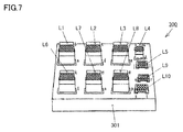
- FIG. 7 is a perspective view of the duplexer 300 described in Patent Document 1.
- the duplexer 300 includes a multilayer body 301 such as a low-temperature fired ceramic multilayer substrate, and inductors L1 to L10.
- a capacitor and an inductor are formed by an internal conductor.
- the inductors L1 to L10 are connected to the upper surface of the multilayer body 301 in a state where the multilayer body 301 is a collective substrate. Thereafter, the collective substrate to which the inductors L1 to L10 are connected is diced or broken to the size of each multilayer body 301, and the duplexer 300 is completed.
- circuit boards separated after dicing or breaking are not aligned.
- circuit boards often have front / back, left / right orientations, and circuit boards need to be realigned in order to connect electronic components to the same main surface of each circuit board. As a result, cost and labor are required.
- an object of the present invention is to provide a circuit board that can be connected to electronic components without requiring rearrangement even if the assembled board is cut and separated into pieces, and an electronic circuit using the circuit board Is to provide modules.
- the structure of the circuit board can be improved so that electronic components can be connected without requiring rearrangement even if the assembled board is cut and separated into pieces. .
- a circuit board according to an aspect of the present invention includes a circuit board main body and first to fourth electrodes.
- the circuit board body includes an internal circuit.
- the first electrode includes a first land electrode and a second land electrode to which an electronic component can be connected.
- the third electrode includes a third land electrode and a fourth land electrode, respectively, to which electronic components can be connected.
- the circuit board body has a rectangular parallelepiped shape having a first surface to a sixth surface.
- the first surface and the second surface are rectangular shapes facing each other.
- the third surface and the fourth surface are orthogonal to the first surface and the second surface and face each other, and extend along the longitudinal sides of the first surface and the second surface.
- the fifth surface and the sixth surface are opposed to each other perpendicular to the first surface to the fourth surface.
- the first electrode and the second electrode are provided on the first surface, and the second electrode is disposed between the first land electrode and the second land electrode.
- the third electrode and the fourth electrode are provided on the second surface, and the fourth electrode is disposed between the third land electrode and the fourth land electrode.
- the first electrode and the third electrode have a 180 ° rotationally symmetric shape with respect to each of the first axis and the second axis.
- the first axis is an axis that passes through the center of gravity of the first surface and the second surface and is orthogonal to the first surface and the second surface.
- the second axis is an axis that passes through the center of gravity of the fifth surface and the sixth surface and is orthogonal to the fifth surface and the sixth surface.
- the internal circuit is configured to be the same electronic circuit when the electronic component is connected to the first electrode and when the electronic component is connected to the third electrode.
- the circuit board according to the present invention preferably has the following features. That is, the first electrode further includes a fifth land electrode and a sixth land electrode to which electronic components can be connected, respectively.
- the fifth land electrode is provided between the first land electrode and the connection portion between the first surface and the fifth surface.
- the sixth land electrode is provided between the second land electrode and the connection portion between the first surface and the sixth surface.
- the third electrode further includes a seventh land electrode and an eighth land electrode to which electronic components can be connected, respectively.
- the seventh land electrode is provided between the third land electrode and the connection portion between the second surface and the fifth surface.
- the eighth land electrode is provided between the fourth land electrode and the connecting portion of the second surface and the sixth surface.
- the first electrode and the third electrode have the above-described characteristics. Therefore, in addition to the above-described effects, an electronic circuit module can be arrayed.
- the circuit board and preferred embodiments thereof according to the present invention preferably have the following features. That is, the second electrode and the fourth electrode have mirror-symmetric shapes with respect to virtual symmetry planes that are the same distance from the first surface and the second surface, respectively.
- the second electrode and the fourth electrode have the above characteristics. Therefore, in addition to the above-described effects, the electronic component is either the first electrode or the third electrode.
- the input side and the output side of the electronic circuit module connected to can be easily distinguished.
- the present invention is also directed to an electronic circuit module.
- an electronic component is connected to the circuit board according to the present invention and the first electrode or the third electrode of the preferred embodiment.
- the above electronic circuit module is smaller than the electronic circuit module obtained by connecting the electronic components in a collective substrate state and then separating them.
- a circuit board includes a circuit board body having an internal circuit, a first electrode to which an electronic component can be connected, and a third electrode to which the electronic component can be connected.
- the circuit board main body has a first surface and a second surface facing each other, the first electrode is provided on the first surface, and the third electrode is provided on the second surface.
- the first electrode and the third electrode are arranged to be mirror-symmetric with respect to virtual symmetry planes that are the same distance from the first surface and the second surface, respectively.
- the internal circuit is configured to be the same electronic circuit when the electronic component is connected to the first electrode and when the electronic component is connected to the third electrode.
- the circuit board according to the present invention since the first electrode and the third electrode have the above-described characteristics, the rearrangement is performed even when the aggregated substrate is cut and separated into pieces. It is possible to connect the electronic components without the need.
- the electronic circuit module using the circuit board according to the present invention is smaller than the electronic circuit module obtained by connecting the electronic components in the state of the collective board and then separating them.
- FIG. 1 is a perspective view of a circuit board 100 which is an embodiment of a circuit board according to the present invention.
- FIG. 2 is a top view of the circuit board 100 as viewed from the first surface side of the circuit board body 1.
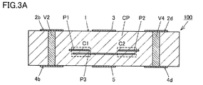
- FIG. 3 is a cross-sectional view of the circuit board 100 taken along arrows IIIA-IIIA in FIG.
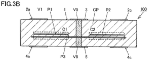
- FIG. 3 is a cross-sectional view of the circuit board 100 taken along the line IIIB-IIIB in FIG. 3 is a cross-sectional view of the circuit board 100 taken along the line IIIC-IIIC in FIG.
- It is a perspective view of circuit board 100A which is the 1st modification of embodiment of a circuit board concerning this invention.
- circuit board 100B which is the 2nd modification of embodiment of a circuit board concerning this invention.
- LC composite filter 200 which is an embodiment of an electronic circuit module concerning this invention.
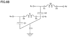
- 2 is a circuit diagram of an LC composite filter 200.
- FIG. 1 is a perspective view of a branching filter (electronic circuit module) 300 of background art.
- circuit board to which the present invention is applied include, but are not limited to, a circuit board such as a low-temperature fired ceramic multilayer board that is a component of an LC composite filter together with an inductor.
- circuit board 100 which is an embodiment of a circuit board according to the present invention will be described with reference to FIGS.
- FIGS. Note that the drawings used hereinafter are simplified, and do not reflect the tailing shape of the electrode and the variation of the shape generated in the manufacturing process. That is, the drawings used hereinafter are for explaining the main part of the present invention, and even if there are different parts from the actual product, they represent the actual product in an essential aspect. Can do.
- FIG. 1 is a perspective view of the circuit board 100.
- the circuit board 100 includes a circuit board body 1, a first electrode 2, a second electrode 3, a third electrode 4, and a fourth electrode 5.
- the circuit board body 1 includes an internal circuit (not shown) including a pattern conductor and a via conductor, as will be described later.
- the first electrode 2 includes first land electrodes 2a and 2b and second land electrodes 2c and 2d, respectively, to which electronic components can be connected.
- the third electrode 4 includes third land electrodes 4a and 4b and fourth land electrodes 4c and 4d, respectively, to which electronic components can be connected.
- each land electrode is a pair of electrodes to which a two-terminal electronic component can be connected.
- the present invention is not limited to this, and when a multi-terminal electronic component is connected, an electrode group corresponding to the number of terminals and Is done.
- the second electrode 3 and the fourth electrode 5 are grounding electrodes.
- one and the other of the land electrodes have a square shape in plan view (see FIG. 2 described later).
- the second electrode 3 and the fourth electrode 5 are each rectangular in plan view (see FIG. 2 described later).
- Examples of materials for the first electrode 2, the second electrode 3, the third electrode 4, and the fourth electrode 5 include noble metals such as Ag, Pd, Pt, and Au, and Cu, Ni, Al, W, Ti, and the like.
- the base metal simple substance or the alloy containing these is used.
- the material of each external electrode is not limited to these.
- Each electrode may be provided with a plating film containing Ni, Sn, or the like.
- the circuit board body 1 has a rectangular parallelepiped shape having a first surface to a sixth surface.
- the first surface and the second surface are rectangular shapes facing each other.
- the third surface and the fourth surface are orthogonal to the first surface and the second surface and face each other, and extend along the longitudinal sides of the first surface and the second surface.
- the fifth surface and the sixth surface are opposed to each other perpendicular to the first surface to the fourth surface.
- the “rectangular shape”, “rectangular shape”, and “orthogonal” in this specification are concepts including slight distortion and deviation due to manufacturing variations of products as described above.
- the first electrode 2 and the second electrode 3 are provided on the first surface (the upper surface of the circuit board body 1 in FIG. 1), and the second electrode 3 includes the first land electrodes 2a and 2b and the second electrode 3 Between the two land electrodes 2c and 2d.
- the third electrode 4 and the fourth electrode 5 are provided on the second surface (the lower surface of the circuit board main body 1 in FIG. 1), and the fourth electrode 5 is the third land electrodes 4a, 4b and the second electrode. 4 land electrodes 4c and 4d.
- the first electrode 2 and the third electrode 4 have a 180 ° rotationally symmetric shape with respect to each of the first axis A and the second axis B.
- the first axis A is an axis that passes through the center of gravity of the first surface and the second surface and is orthogonal to the first surface and the second surface.
- the second axis B is an axis that passes through the center of gravity of the fifth surface and the sixth surface and is orthogonal to the fifth surface and the sixth surface.
- 180 ° rotational symmetry as used in this specification is a concept including a state that can be regarded as having a substantially symmetrical relationship based on slight distortion and deviation due to manufacturing variations of products as described above. It is.
- the “centroid” can be defined as an intersection of diagonal lines of each surface of the rectangle, but is a concept including a point that can be regarded as a position of the center of gravity substantially for the same reason as described above.
- the internal circuit is configured to be the same electronic circuit when the electronic component is connected to the first electrode 2 and when the electronic component is connected to the third electrode 4.
- An example of the circuit configuration will be described with reference to FIGS. 2 and 3A to 3C.
- FIG. 2 is a top view of the circuit board 100 as viewed from the first surface side of the circuit board body 1.
- 3A is a cross-sectional view of the circuit board 100 taken along the line IIIA-IIIA in FIG. 3B is a cross-sectional view of the circuit board 100 taken along the line IIIB-IIIB in FIG. 3C is a cross-sectional view of the circuit board 100 taken along the line IIIC-IIIC in FIG.
- the circuit board body 1 includes a ceramic portion CP, pattern conductors P1 to P3, and via conductors V1 to V8.
- a so-called low-temperature fired ceramic material which is a Ba—Al—Si—Mn-based oxide is used.
- the material of the pattern conductors P1 to P3 and the via conductors V1 to V8 is, for example, a noble metal such as Ag, Pd, Pt, or Au and a base metal such as Cu, Ni, Al, W, or Ti, or an alloy containing these. Is used.
- the material of each component is not limited to these.
- One first land electrode 2a is connected to one third land electrode 4a through a via conductor V1, a pattern conductor P1, and a via conductor V6.
- the other first land electrode 2b is connected to the other third land electrode 4b through a via conductor V2.
- One second land electrode 2c is connected to one fourth land electrode 4c through a via conductor V3, a pattern conductor P2, and a via conductor V7.
- the other second land electrode 2d is connected to the other fourth land electrode 4d through a via conductor V4.
- the second electrode 3 is connected to the fourth electrode 5 via the via conductor V5, the pattern conductor P3, and the via conductor V8.
- the area where the pattern conductor P1 and the pattern conductor P3 overlap when viewed from the first surface side of the circuit board body 1 is a capacitor C1 (hatched area in FIG. 2).
- a region where the pattern conductor P2 and the pattern conductor P3 overlap each other is a capacitor C2 (same as above).
- an LC composite filter including two so-called low-pass filters. (See FIGS. 6A and 6B). In this case, the two low-pass filters share the fourth electrode 5 as a grounding electrode.
- the same LC composite filter is configured.
- the two low-pass filters share the second electrode 3 as a grounding electrode.
- the electronic components can be connected without requiring rearrangement.
- circuit board 100A which is a first modification of the embodiment of the circuit board according to the present invention will be described with reference to FIG.
- the circuit board 100A differs from the circuit board 100 described above in the shapes of the second electrode 3 and the fourth electrode 5. Since the rest is common to the circuit board 100, the description of common parts may be omitted or simplified. In the following description, the description of common parts is the same.
- FIG. 4 is a perspective view of a circuit board 100A which is a first modification of the embodiment of the circuit board according to the present invention.
- the second electrode 3 in the circuit board 100A has a side 3p formed by cutting out one of four corners of a rectangle.
- the fourth electrode 5 has a side 5p formed by cutting out one of four corners of a rectangle.
- the second electrode 3 and the fourth electrode 5 having such a shape are mirror-symmetric with respect to virtual symmetry planes that are at the same distance from the first surface and the second surface, respectively.
- the second electrode 3 and the fourth electrode 5 have the above characteristics. Therefore, in addition to the effects obtained by the circuit board 100, the input side and the output side of the electronic circuit module in which the electronic component is connected to either the first electrode 2 or the third electrode 4 can be easily distinguished. it can.
- the LC composite filter including the above-described low-pass filter has an asymmetric configuration, and the effect changes when the input and output are reversed, so care must be taken when using it.
- the LC composite filter using the circuit board 100A input / output reversal can be reliably prevented.
- the shape of the 2nd electrode 3 and the 4th electrode 5 is not restricted to what was shown by FIG. 4, and can be made into arbitrary shapes.
- circuit board 100B which is a second modification of the embodiment of the circuit board according to the present invention will be described with reference to FIG.
- the circuit board 100A is different from the above-described circuit boards 100 and 100A in the configuration of the first electrode 2 and the third electrode 4, and is otherwise common.
- FIG. 5 is a perspective view of a circuit board 100B which is a second modification of the embodiment of the circuit board according to the present invention.
- the first electrode 2 in the circuit board 100B further includes fifth land electrodes 2e and 2f and sixth land electrodes 2g and 2h to which electronic components can be connected, respectively.
- the fifth land electrodes 2e and 2f are provided between the first land electrodes 2a and 2b and the first surface and the connecting portion of the fifth surface (ridge line between the first surface and the fifth surface).
- the sixth land electrodes 2g and 2h are provided between the second land electrodes 2c and 2d and the first surface and the connection portion of the sixth surface (the ridge line between the first surface and the sixth surface). Yes.
- the third electrode 4 further includes seventh land electrodes 4e and 4f and eighth land electrodes 4g and 4h, respectively, to which electronic components can be connected.
- the seventh land electrodes 4e and 4f are provided between the third land electrodes 4a and 4b and the connection portions (ridge lines between the second surface and the fifth surface) of the second surface and the fifth surface.
- the eighth land electrodes 4g and 4h are provided between the fourth land electrodes 4c and 4d and the connection portion between the second surface and the sixth surface (ridge line between the second surface and the sixth surface). Yes.
- the first electrode 2 and the third electrode 4 have the above characteristics. Therefore, in addition to the effects obtained with the circuit board 100, an electronic circuit module can be arrayed.
- an LC composite filter 200 is shown as an example of an embodiment of the electronic circuit module according to the present invention. Needless to say, the present invention is not limited to the LC composite filter 200 and is applied to various types of electronic circuit modules.
- FIG. 6A is a perspective view of the LC composite filter 200.
- FIG. 6B is a circuit diagram of the LC composite filter 200.
- the first inductor 6 is connected to the first land electrodes 2a and 2b of the circuit board 100A (see FIG. 4), and the second inductor 10 is connected to the second land electrodes 2c and 2d. It becomes.
- the circuit board 100A includes an internal circuit (not shown) shown in FIGS. 2 and 3A to 3C.
- the first inductor 6 includes an inductor body 7 and external electrodes 8 and 9.
- the second inductor 10 includes an inductor element body 11 and external electrodes 12 and 13.
- One external electrode 8 of the first inductor 6 is connected to one first land electrode 2a, and the other external electrode 9 is connected to the other first land electrode 2b.
- One external electrode 12 of the second inductor 10 is connected to one second land electrode 2c, and the other external electrode 13 is connected to the other second land electrode 2d.
- an LC composite filter 200 including two low-pass filters that share the fourth electrode 5 as a ground electrode is configured.
- the first inductor 6 is connected to the third land electrodes 4a and 4b and the second inductor 10 is connected to the fourth land electrodes 4c and 4d, the same LC composite filter 200 is configured. Is done. In this case, the two low-pass filters share the second electrode 3 as a grounding electrode.
- the LC composite filter 200 is manufactured by connecting the first inductor 6 and the second inductor 10 to an individual circuit board 100A.
- a wide margin area where each inductor is not connected to the circuit board is taken in order to prevent damage to each inductor in the cutting process. is required.
- the LC composite filter 200 it is not necessary to provide a wide margin area on the circuit board 100A. Therefore, the size is reduced as compared with the LC composite filter obtained by connecting each inductor in a collective substrate state and then separating the inductors.
- the LC composite filter 200 may include a protective layer that covers each electrode disposed on the first surface of the circuit board body 1 and the first inductor 6 and the second inductor 10. In this case, the protective layer may not cover the entire first surface.
Landscapes
- Engineering & Computer Science (AREA)
- Microelectronics & Electronic Packaging (AREA)
- Structures For Mounting Electric Components On Printed Circuit Boards (AREA)
Abstract
回路基板(100)は、第1面ないし第6面を有する直方体形状の回路基板本体(1)と、第1面に設けられ第1のランド電極(2a,2b)および第2のランド電極(2c,2d)を含む第1の電極(2)と、第2面に設けられ第3のランド電極(4a,4b)および第4のランド電極(4c,4d)を含む第3の電極(4)とを備える。第1の電極(2)および第3の電極(4)は、第1面および第2面の重心を通り第1面および第2面と直交する第1の軸(A)および第5面および第6面の重心を通り第5面および第6面と直交する第2の軸(B)について、180°回転対称の形状を有している。内部回路は、第1の電極(2)に電子部品が接続された場合と第3の電極(4)に同じ電子部品が接続された場合とで、同一の電子回路となるように構成されている。
Description
この発明は、回路基板および電子回路モジュールに関する。より特定的には、予め個片化された状態で、電子部品が接続される回路基板およびそれを用いた電子回路モジュールに関する。
低温焼成セラミック多層基板などの回路基板上に、電子部品が接続された電子回路モジュールの製造においては、通常、回路基板がいわゆる集合基板の状態で電子部品が接続され、その後、個々の電子回路モジュールに切断される。
一例として、特開2014-179967号公報(特許文献1)に記載の分波器について説明する。図7は、特許文献1に記載の分波器300の斜視図である。分波器300は、たとえば低温焼成セラミック多層基板のような積層体301と、インダクタL1ないしL10とを含んでなる。積層体301の内部には、コンデンサおよびインダクタが、内部導体によって形成されている。インダクタL1ないしL10は、積層体301が集合基板の状態で、積層体301の上面に接続される。その後、インダクタL1ないしL10が接続された集合基板は、個々の積層体301の大きさにダイシングまたはブレイクされ、分波器300が完成する。
上記の切断工程におけるインダクタL1ないしL10の破損を防ぐためには、積層体301の上面に、インダクタL1ないしL10が接続されないマージン領域を広く取ることが必要である。そのため、上記の製造方法では、分波器300の小型化が困難となっている。このことは、同様の製造方法によって製造される電子回路モジュールにおいて、共通の課題となっている。
電子回路モジュールの小型化を図るためには、切断工程による影響を受けないように、回路基板が予め個片化された状態で、電子部品の接続が行なわれる必要がある。しかしながら、ダイシング後またはブレイク後で個片化された回路基板は、整列状態ではなくなる。通常、回路基板は表裏左右の方向性を有することが多く、個々の回路基板の同じ主面に電子部品が接続されるようにするためには、回路基板の再整列が必要となる。その結果、コストおよび手間が掛かってしまう。
そこで、この発明の目的は、集合基板の状態から切断されて個片化された状態となっても、再配列を要することなく電子部品の接続が可能な回路基板と、それを用いた電子回路モジュールを提供することである。
この発明では、集合基板の状態から切断されて個片化された状態となっても、再配列を要することなく電子部品の接続が可能となるように、回路基板の構造についての改良が図られる。
この発明は、まず回路基板に向けられる。
この発明のある局面に係る回路基板は、回路基板本体と、第1ないし第4の電極と、を備えている。回路基板本体は、内部回路を備えている。第1の電極は、それぞれ電子部品が接続可能な第1のランド電極および第2のランド電極を含んでいる。第3の電極は、それぞれ電子部品が接続可能な第3のランド電極および第4のランド電極を含んでいる。
この発明のある局面に係る回路基板は、回路基板本体と、第1ないし第4の電極と、を備えている。回路基板本体は、内部回路を備えている。第1の電極は、それぞれ電子部品が接続可能な第1のランド電極および第2のランド電極を含んでいる。第3の電極は、それぞれ電子部品が接続可能な第3のランド電極および第4のランド電極を含んでいる。
回路基板本体は、第1面ないし第6面を有する直方体形状である。第1面および第2面は、互いに対向する長方形状である。第3面および第4面は、第1面および第2面に直交して互いに対向し、第1面および第2面の長手側の辺に沿っている。第5面および第6面は、第1面ないし第4面に直交して互いに対向している。第1の電極および第2の電極は、第1面に設けられており、かつ第2の電極が第1のランド電極および第2のランド電極の間に配置されている。第3の電極および第4の電極は、第2面に設けられており、かつ第4の電極が第3のランド電極および第4のランド電極の間に配置されている。
第1の電極および第3の電極は、第1の軸および第2の軸のそれぞれについて、180°回転対称の形状を有している。第1の軸とは、第1面および第2面の重心を通り第1面および第2面と直交する軸のことである。また、第2の軸とは、第5面および第6面の重心を通り第5面および第6面と直交する軸のことである。そして、内部回路は、第1の電極に電子部品が接続された場合と、第3の電極に当該電子部品が接続された場合とで、同一の電子回路となるように構成されている。
上記の回路基板は、第1の電極と第3の電極とが上記の特徴を有しているため、集合基板の状態から切断されて個片化された状態となっても、再配列を要することなく電子部品の接続が可能である。
この発明に係る回路基板は、以下の特徴を備えることが好ましい。すなわち、第1の電極は、それぞれ電子部品が接続可能な第5のランド電極と第6のランド電極とをさらに含んでいる。第5のランド電極は、第1のランド電極と第1面および第5面の接続部との間に設けられている。第6のランド電極は、第2のランド電極と第1面および第6面の接続部との間に設けられている。また、第3の電極は、それぞれ電子部品が接続可能な第7のランド電極と第8のランド電極とをさらに含んでいる。第7のランド電極は、第3のランド電極と第2面および第5面の接続部との間に設けられている。第8のランド電極は、第4のランド電極と第2面および第6面の接続部との間に設けられている。
上記の回路基板は、第1の電極と第3の電極とが上記の特徴を有しているため、前述の効果に加えて、電子回路モジュールのアレイ化が可能となる。
この発明に係る回路基板およびその好ましい実施形態は、以下の特徴を備えることが好ましい。すなわち、第2の電極および第4の電極は、第1面および第2面からそれぞれ同じ距離にある仮想的な対称面について、鏡面対称の形状を有している。
上記の回路基板は、第2の電極と第4の電極とが上記の特徴を有しているため、前述の効果に加えて、電子部品が第1の電極または第3の電極のいずれか一方に接続されてなる電子回路モジュールの入力側と出力側とが容易に判別できる。
この発明は、また電子回路モジュールにも向けられる。
この発明に係る電子回路モジュールは、この発明に係る回路基板およびその好ましい実施形態の第1の電極または第3の電極に、電子部品が接続されてなる。
この発明に係る電子回路モジュールは、この発明に係る回路基板およびその好ましい実施形態の第1の電極または第3の電極に、電子部品が接続されてなる。
上記の電子回路モジュールは、集合基板の状態で電子部品を接続した後、個片化することにより得られる電子回路モジュールに比べて、小型化されている。
この発明の他の局面に係る回路基板は、内部回路を備える回路基板本体と、電子部品が接続可能な第1の電極と、電子部品が接続可能な第3の電極とを備えている。回路基板本体は、互いに対向する第1面および第2面を有し、第1の電極は、第1面に設けられており、第3の電極は、第2面に設けられている。第1の電極および第3の電極は、第1面および第2面からそれぞれ同じ距離にある仮想的な対称面について、鏡面対称となるように配置されている。内部回路は、第1の電極に電子部品が接続された場合と、第3の電極に当該電子部品が接続された場合とで、同一の電子回路となるように構成されている。
この発明に係る回路基板は、第1の電極と第3の電極とが上記の特徴を有しているため、集合基板の状態から切断されて個片化された状態となっても、再配列を要することなく電子部品の接続が可能である。また、この発明に係る回路基板を用いた電子回路モジュールは、集合基板の状態で電子部品を接続した後、個片化することにより得られる電子回路モジュールに比べて、小型化されている。
以下にこの発明の実施形態を示して、この発明の特徴とするところをさらに詳しく説明する。この発明が適用される回路基板としては、たとえばインダクタと共にLC複合フィルタの構成要素となる低温焼成セラミック多層基板のような回路基板が挙げられるが、これに限られるものではない。
-回路基板の実施形態-
この発明に係る回路基板の実施形態である回路基板100について、図1および図2を用いて説明する。なお、以後で用いる図面は、簡略化されたものであり、電極の裾引き形状および製造工程上で発生する形状のばらつきなどは反映されていない。すなわち、以後で用いる図面は、この発明の要部を説明するためのものであって、たとえ実際の製品と異なる部分があったとしても、本質的な面で実際の製品を表すものと言うことができる。
この発明に係る回路基板の実施形態である回路基板100について、図1および図2を用いて説明する。なお、以後で用いる図面は、簡略化されたものであり、電極の裾引き形状および製造工程上で発生する形状のばらつきなどは反映されていない。すなわち、以後で用いる図面は、この発明の要部を説明するためのものであって、たとえ実際の製品と異なる部分があったとしても、本質的な面で実際の製品を表すものと言うことができる。
図1は、回路基板100の斜視図である。回路基板100は、回路基板本体1と、第1の電極2と、第2の電極3と、第3の電極4と、第4の電極5と、を備えている。
回路基板本体1は、後述するように、パターン導体とビア導体とを含む内部回路(不図示)を備えている。第1の電極2は、それぞれ電子部品が接続可能な第1のランド電極2a,2bおよび第2のランド電極2c,2dを含んでいる。第3の電極4は、それぞれ電子部品が接続可能な第3のランド電極4a,4bおよび第4のランド電極4c,4dを含んでいる。回路基板100では、各ランド電極は、2端子電子部品が接続できる一対の電極であるが、これに限られず、多端子電子部品が接続される場合は、その端子の数に応じた電極群とされる。第2の電極3および第4の電極5は、接地用電極である。
回路基板100において、各ランド電極の一方および他方は、それぞれ平面視で正方形状(後述の図2参照)である。また、第2の電極3および第4の電極5は、それぞれ平面視で長方形状(後述の図2参照)である。
第1の電極2、第2の電極3、第3の電極4および第4の電極5の材質としては、たとえばAg、Pd、Pt、Auなどの貴金属およびCu、Ni、Al、W、Tiなどの卑金属の単体、あるいはこれらを含む合金が用いられる。ただし、それぞれの外部電極の材質は、これらに限られない。なお、それぞれの電極は、Ni、Snなどを含むめっき膜を備えていてもよい。
回路基板本体1は、第1面ないし第6面を有する直方体形状である。第1面および第2面は、互いに対向する長方形状である。第3面および第4面は、第1面および第2面に直交して互いに対向し、第1面および第2面の長手側の辺に沿っている。第5面および第6面は、第1面ないし第4面に直交して互いに対向している。ここで、この明細書で言う「直方体形状」、「長方形状」および「直交」とは、前述したように製品の製造ばらつきなどによる若干の歪み、およびずれを含む概念である。
第1の電極2および第2の電極3は、第1面(図1における回路基板本体1の上面)に設けられており、かつ第2の電極3が第1のランド電極2a,2bおよび第2のランド電極2c,2dの間に配置されている。第3の電極4および第4の電極5は、第2面(図1における回路基板本体1の下面)に設けられており、かつ第4の電極5が第3のランド電極4a,4bおよび第4のランド電極4c,4dの間に配置されている。
第1の電極2および第3の電極4は、第1の軸Aおよび第2の軸Bのそれぞれについて、180°回転対称の形状を有している。ここで、第1の軸Aとは、第1面および第2面の重心を通り第1面および第2面と直交する軸のことである。また、第2の軸Bとは、第5面および第6面の重心を通り第5面および第6面と直交する軸のことである。ここで、この明細書で言う「180°回転対称」とは、前述したように製品の製造ばらつきなどによる若干の歪み、およびずれを踏まえて、実質的に対称関係にあると見なせる状態を含む概念である。また、「重心」は、長方形の各面の対角線の交点として定義できるが、上記と同様の理由により実質的に重心位置と見なせる点を含む概念である。
そして、内部回路は、第1の電極2に電子部品が接続された場合と、第3の電極4に電子部品が接続された場合とで、同一の電子回路となるように構成されている。当該回路構成の一例について、図2および図3Aから図3Cを用いて説明する。
図2は、回路基板100を回路基板本体1の第1面側から見た上面図である。図3Aは、回路基板100の図2におけるIIIA-IIIA矢視断面図である。図3Bは、回路基板100の図2におけるIIIB-IIIB矢視断面図である。図3Cは、回路基板100の図2におけるIIIC-IIIC矢視断面図である。
回路基板本体1は、セラミック部CPと、パターン導体P1ないしP3と、ビア導体V1ないしV8とを備えている。セラミック部CPの材質としては、例えばBa-Al-Si-Mn系酸化物である、いわゆる低温焼成セラミック材料が用いられる。また、パターン導体P1ないしP3およびビア導体V1ないしV8の材質としては、例えばAg、Pd、Pt、Auなどの貴金属およびCu、Ni、Al、W、Tiなどの卑金属の単体、あるいはこれらを含む合金が用いられる。ただし、それぞれの構成要素の材質は、これらに限られない。
一方の第1のランド電極2aは、ビア導体V1、パターン導体P1およびビア導体V6を介して、一方の第3のランド電極4aと接続されている。他方の第1のランド電極2bは、ビア導体V2を介して、他方の第3のランド電極4bと接続されている。一方の第2のランド電極2cは、ビア導体V3、パターン導体P2およびビア導体V7を介して、一方の第4のランド電極4cと接続されている。他方の第2のランド電極2dは、ビア導体V4を介して、他方の第4のランド電極4dと接続されている。第2の電極3は、ビア導体V5、パターン導体P3およびビア導体V8を介して、第4の電極5と接続されている。
パターン導体P1とパターン導体P3とが回路基板本体1の第1面側から見て重なった領域は、コンデンサC1となっている(図2のハッチング領域)。また、同じくパターン導体P2とパターン導体P3とが重なった領域は、コンデンサC2となっている(同上)。
回路基板本体1に上記のような内部回路が構成されている場合、第1の電極2に電子部品が接続された場合と、第3の電極4に当該電子部品が接続された場合とで、同一の電子回路となる。例えば、第1のランド電極2a,2bに第1のインダクタが接続され、第2のランド電極2c,2dに第2のインダクタが接続された場合、いわゆるローパスフィルタを2回路備えているLC複合フィルタが構成される(図6Aおよび図6B参照)。この場合、2つのローパスフィルタは、第4の電極5を接地用電極として共用している。
一方、第3のランド電極4a,4bに第1のインダクタが接続され、第4のランド電極4c,4dに第2のインダクタが接続された場合においても、同様のLC複合フィルタが構成される。この場合、2つのローパスフィルタは、第2の電極3を接地用電極として共用することになる。
すなわち、回路基板100は、集合基板の状態から切断されて個片化された状態となっても、再配列を要することなく電子部品の接続が可能である。
-回路基板の実施形態の第1の変形例-
この発明に係る回路基板の実施形態の第1の変形例である回路基板100Aについて、図4を用いて説明する。回路基板100Aは、第2の電極3および第4の電極5の形状が、前述の回路基板100と異なっている。それ以外は回路基板100と共通であるため、共通する箇所の説明については省略または簡略化することがある。以後の説明においても、共通する箇所の説明については同様である。
この発明に係る回路基板の実施形態の第1の変形例である回路基板100Aについて、図4を用いて説明する。回路基板100Aは、第2の電極3および第4の電極5の形状が、前述の回路基板100と異なっている。それ以外は回路基板100と共通であるため、共通する箇所の説明については省略または簡略化することがある。以後の説明においても、共通する箇所の説明については同様である。
図4は、この発明に係る回路基板の実施形態の第1の変形例である回路基板100Aの斜視図である。回路基板100Aにおける第2の電極3は、長方形の4つの角のうちの1つが切り欠かれてなる辺3pを有している。同様に、第4の電極5は、長方形の4つの角のうちの1つが切り欠かれてなる辺5pを有している。さらに、そのような形状を有する第2の電極3および第4の電極5は、第1面および第2面からそれぞれ同じ距離にある仮想的な対称面について、鏡面対称となっている。
回路基板100Aは、第2の電極3および第4の電極5が上記の特徴を有している。そのため、回路基板100で得られる効果に加えて、電子部品が第1の電極2または第3の電極4のいずれか一方に接続されてなる電子回路モジュールの入力側と出力側とが容易に判別できる。
たとえば、前述のローパスフィルタを備えているLC複合フィルタは非対称の構成となっており、入力と出力が逆転すると効果が変わってしまうため、使用する際には注意が必要である。一方、回路基板100Aを用いたLC複合フィルタでは、入出力逆転を確実に防止することができる。なお、第2の電極3および第4の電極5の形状は、図4に示されたものに限らず、任意の形状とすることができる。
-回路基板の実施形態の第2の変形例-
この発明に係る回路基板の実施形態の第2の変形例である回路基板100Bについて、図5を用いて説明する。回路基板100Aは、第1の電極2および第3の電極4の構成が、前述の回路基板100,100Aと異なっており、それ以外は共通である。
この発明に係る回路基板の実施形態の第2の変形例である回路基板100Bについて、図5を用いて説明する。回路基板100Aは、第1の電極2および第3の電極4の構成が、前述の回路基板100,100Aと異なっており、それ以外は共通である。
図5は、この発明に係る回路基板の実施形態の第2の変形例である回路基板100Bの斜視図である。回路基板100Bにおける第1の電極2は、それぞれ電子部品が接続可能な第5のランド電極2e,2fと第6のランド電極2g,2hとをさらに含んでいる。第5のランド電極2e,2fは、第1のランド電極2a,2bと第1面および第5面の接続部(第1面と第5面との間の稜線)との間に設けられている。第6のランド電極2g,2hは、第2のランド電極2c,2dと第1面および第6面の接続部(第1面と第6面との間の稜線)との間に設けられている。
また、第3の電極4は、それぞれ電子部品が接続可能な第7のランド電極4e,4fと第8のランド電極4g,4hとをさらに含んでいる。第7のランド電極4e,4fは、第3のランド電極4a,4bと第2面および第5面の接続部(第2面と第5面との間の稜線)との間に設けられている。第8のランド電極4g,4hは、第4のランド電極4c,4dと第2面および第6面の接続部(第2面と第6面との間の稜線)との間に設けられている。
回路基板100Bは、第1の電極2および第3の電極4が上記の特徴を有している。そのため、回路基板100で得られる効果に加えて、電子回路モジュールのアレイ化が可能となる。
-電子回路モジュールの実施形態-
この発明に係る電子回路モジュールの実施形態について、図6Aおよび図6Bを用いて説明する。図6Aおよび図6Bでは、この発明に係る電子回路モジュールの実施形態の一例として、LC複合フィルタ200が図示されている。なお、この発明は、LC複合フィルタ200に限らず、種々の形態の電子回路モジュールに適用されることは言うまでもない。
この発明に係る電子回路モジュールの実施形態について、図6Aおよび図6Bを用いて説明する。図6Aおよび図6Bでは、この発明に係る電子回路モジュールの実施形態の一例として、LC複合フィルタ200が図示されている。なお、この発明は、LC複合フィルタ200に限らず、種々の形態の電子回路モジュールに適用されることは言うまでもない。
図6Aは、LC複合フィルタ200の斜視図である。図6Bは、LC複合フィルタ200の回路図である。LC複合フィルタ200は、回路基板100A(図4参照)の第1のランド電極2a,2bに第1のインダクタ6が接続され、第2のランド電極2c,2dに第2のインダクタ10が接続されてなる。なお、回路基板100Aは、図2および図3Aから図3Cに示された内部回路(不図示)を備えている。
第1のインダクタ6は、インダクタ素体7と、外部電極8,9とを備えている。第2のインダクタ10は、インダクタ素体11と、外部電極12,13とを備えている。第1のインダクタ6の一方の外部電極8は、一方の第1のランド電極2aと接続されており、他方の外部電極9は、他方の第1のランド電極2bと接続されている。第2のインダクタ10の一方の外部電極12は、一方の第2のランド電極2cと接続されており、他方の外部電極13は、他方の第2のランド電極2dと接続されている。
その結果、図6Bに示されているように、第4の電極5を接地用電極として共用しているローパスフィルタを2回路備えているLC複合フィルタ200が構成される。一方、第3のランド電極4a,4bに第1のインダクタ6が接続され、第4のランド電極4c,4dに第2のインダクタ10が接続された場合においても、同様のLC複合フィルタ200が構成される。この場合、2つのローパスフィルタは、第2の電極3を接地用電極として共用することになる。
なお、非対称の構成を有するLC複合フィルタでは、入力と出力が逆転すると効果が変わってしまう。一方、図6Aおよび図6Bに示されているLC複合フィルタ200では、回路基板100Aが用いられているので、前述したように入出力逆転を確実に防止することができる。
LC複合フィルタ200は、個片化された回路基板100Aに第1のインダクタ6および第2のインダクタ10が接続されることにより製造される。集合基板の状態で各インダクタを接続した後、個片化することにより得られるLC複合フィルタでは、切断工程における各インダクタの破損を防ぐために、回路基板に各インダクタが接続されないマージン領域を広く取ることが必要である。一方、LC複合フィルタ200では、回路基板100Aにマージン領域を広く取る必要がない。そのため、集合基板の状態で各インダクタを接続した後、個片化して得られるLC複合フィルタに比べて、小型化されている。
なお、LC複合フィルタ200は、回路基板本体1の第1面上に配置されている各電極、ならびに第1のインダクタ6および第2のインダクタ10を被覆する保護層を備えていてもよい。この場合、保護層は、第1面全体を被覆していなくてもよい。
なお、この発明は上記の実施形態に限定されるものではなく、この発明の範囲内において、種々の応用、変形を加えることができる。また、この明細書に記載の各実施形態は、例示的なものであり、異なる実施形態間において、構成の部分的な置換または組み合わせが可能である。
1 回路基板本体、2 第1の電極、2a,2b 第1のランド電極、2c,2d 第2のランド電極、3 第2の電極、4 第3の電極、4a,4b 第3のランド電極、4c,4d 第4のランド電極、5 第4の電極、6 第1のインダクタ、7,11 インダクタ素体、8,9,12,13 外部電極、10 第2のインダクタ、100,100A,100B 回路基板、200 LC複合フィルタ(電子回路モジュール)、A 第1の軸、B 第2の軸、C1,C2 コンデンサ、CP セラミック部、P1,P2,P3 パターン導体、V1,V2,V3,V4,V5,V6,V7,V8 ビア導体。
Claims (5)
- 内部回路を備える回路基板本体と、それぞれ電子部品が接続可能な第1のランド電極および第2のランド電極を含む第1の電極と、第2の電極と、それぞれ電子部品が接続可能な第3のランド電極および第4のランド電極を含む第3の電極と、第4の電極とを備える回路基板であって、
前記回路基板本体は、互いに対向する長方形状の第1面および第2面と、前記第1面および前記第2面に直交して互いに対向し、前記第1面および前記第2面の長手側の辺に沿う第3面および第4面と、前記第1面ないし前記第4面に直交して互いに対向する第5面および第6面とを有する直方体形状であり、
前記第1の電極および前記第2の電極は、前記第1面に設けられており、かつ前記第2の電極が前記第1のランド電極および前記第2のランド電極の間に配置されており、前記第3の電極および前記第4の電極は、前記第2面に設けられており、前記第4の電極が前記第3のランド電極および前記第4のランド電極の間に配置されており、
前記第1の電極および前記第3の電極は、前記第1面および前記第2面の重心を通り前記第1面および前記第2面と直交する第1の軸および前記第5面および前記第6面の重心を通り前記第5面および前記第6面と直交する第2の軸のそれぞれについて、180°回転対称の形状を有しており、
かつ、前記内部回路は、前記第1の電極に電子部品が接続された場合と、前記第3の電極に当該電子部品が接続された場合とで、同一の電子回路となるように構成されている、回路基板。 - 前記第1の電極は、それぞれ電子部品が接続可能であって、前記第1のランド電極と前記第1面および前記第5面の接続部との間に設けられた第5のランド電極と、前記第2のランド電極と前記第1面および前記第6面の接続部との間に設けられた第6のランド電極とをさらに含み、
前記第3の電極は、それぞれ電子部品が接続可能であって、前記第3のランド電極と前記第2面および前記第5面の接続部との間に設けられた第7のランド電極と、前記第4のランド電極と前記第2面および前記第6面の接続部との間に設けられた第8のランド電極とをさらに含んでいる、請求項1に記載の回路基板。 - 前記第2の電極および前記第4の電極は、前記第1面および前記第2面からそれぞれ同じ距離にある仮想的な対称面について、鏡面対称の形状を有している、請求項1または請求項2に記載の回路基板。
- 請求項1ないし請求項3のいずれか1項に記載の回路基板の前記第1の電極または前記第3の電極に、電子部品が接続されてなる、電子回路モジュール。
- 内部回路を備える回路基板本体と、電子部品が接続可能な第1の電極と、電子部品が接続可能な第3の電極とを備える回路基板であって、
前記回路基板本体は、互いに対向する第1面および第2面を有し、
前記第1の電極は、前記第1面に設けられており、前記第3の電極は、前記第2面に設けられており、
前記第1の電極および前記第3の電極は、前記第1面および前記第2面からそれぞれ同じ距離にある仮想的な対称面について、鏡面対称となるように配置されており、
かつ、前記内部回路は、前記第1の電極に電子部品が接続された場合と、前記第3の電極に当該電子部品が接続された場合とで、同一の電子回路となるように構成されている、回路基板。
Applications Claiming Priority (2)
| Application Number | Priority Date | Filing Date | Title |
|---|---|---|---|
| JP2016057350 | 2016-03-22 | ||
| JP2016-057350 | 2016-03-22 |
Publications (1)
| Publication Number | Publication Date |
|---|---|
| WO2017164062A1 true WO2017164062A1 (ja) | 2017-09-28 |
Family
ID=59900333
Family Applications (1)
| Application Number | Title | Priority Date | Filing Date |
|---|---|---|---|
| PCT/JP2017/010671 Ceased WO2017164062A1 (ja) | 2016-03-22 | 2017-03-16 | 回路基板および電子回路モジュール |
Country Status (1)
| Country | Link |
|---|---|
| WO (1) | WO2017164062A1 (ja) |
Citations (4)
| Publication number | Priority date | Publication date | Assignee | Title |
|---|---|---|---|---|
| JPS5438860U (ja) * | 1977-08-23 | 1979-03-14 | ||
| JPH0231490A (ja) * | 1988-07-20 | 1990-02-01 | Sony Corp | プリント基板集合体 |
| JPH054543U (ja) * | 1991-07-03 | 1993-01-22 | セイコーエプソン株式会社 | 多面付けプリント配線板 |
| JP2008186941A (ja) * | 2007-01-29 | 2008-08-14 | Cmk Corp | 半導体装置とその製造方法 |
-
2017
- 2017-03-16 WO PCT/JP2017/010671 patent/WO2017164062A1/ja not_active Ceased
Patent Citations (4)
| Publication number | Priority date | Publication date | Assignee | Title |
|---|---|---|---|---|
| JPS5438860U (ja) * | 1977-08-23 | 1979-03-14 | ||
| JPH0231490A (ja) * | 1988-07-20 | 1990-02-01 | Sony Corp | プリント基板集合体 |
| JPH054543U (ja) * | 1991-07-03 | 1993-01-22 | セイコーエプソン株式会社 | 多面付けプリント配線板 |
| JP2008186941A (ja) * | 2007-01-29 | 2008-08-14 | Cmk Corp | 半導体装置とその製造方法 |
Similar Documents
| Publication | Publication Date | Title |
|---|---|---|
| CN107039180B (zh) | 电子部件 | |
| US11695388B2 (en) | Elastic wave device | |
| JP6528636B2 (ja) | 積層コイル部品 | |
| US9299498B2 (en) | Miniature wire-bondable capacitor | |
| JP6254071B2 (ja) | コモンモードフィルタ及びコモンモードフィルタが備えられた電子装置 | |
| US11139112B2 (en) | Electronic component | |
| CN107925393A (zh) | 压电振动器件 | |
| WO2015037374A1 (ja) | インダクタおよび帯域除去フィルタ | |
| US11488761B2 (en) | Laminated electronic component | |
| JPWO2013187186A1 (ja) | 電子部品及びその製造方法 | |
| CN111788674A (zh) | 高频模块 | |
| CN105122644B (zh) | 弹性表面波装置 | |
| CN109845101B (zh) | 层叠型lc滤波器阵列 | |
| JP5958454B2 (ja) | 部品内蔵モジュール | |
| KR100880814B1 (ko) | 전자 부품 모듈 | |
| JP2008192808A (ja) | 積層型電子部品の実装構造 | |
| JP2016152392A (ja) | プリント回路板、その製造方法、及びインダクタ製品 | |
| CN106373738B (zh) | 线圈组件 | |
| JP6589446B2 (ja) | 積層コイル部品 | |
| WO2017164062A1 (ja) | 回路基板および電子回路モジュール | |
| KR101823189B1 (ko) | 인덕터 어셈블리 | |
| TW201801472A (zh) | 積層型電子零件 | |
| JP2018170322A (ja) | 電子部品 | |
| JP5968827B2 (ja) | 半導体パッケージおよびその製造方法 | |
| US9058923B2 (en) | Electronic component and manufacturing method thereof |
Legal Events
| Date | Code | Title | Description |
|---|---|---|---|
| NENP | Non-entry into the national phase |
Ref country code: DE |
|
| 121 | Ep: the epo has been informed by wipo that ep was designated in this application |
Ref document number: 17770105 Country of ref document: EP Kind code of ref document: A1 |
|
| 122 | Ep: pct application non-entry in european phase |
Ref document number: 17770105 Country of ref document: EP Kind code of ref document: A1 |
|
| NENP | Non-entry into the national phase |
Ref country code: JP |