WO2017154338A1 - オゾン生成用素子およびオゾン生成装置 - Google Patents
オゾン生成用素子およびオゾン生成装置 Download PDFInfo
- Publication number
- WO2017154338A1 WO2017154338A1 PCT/JP2017/000754 JP2017000754W WO2017154338A1 WO 2017154338 A1 WO2017154338 A1 WO 2017154338A1 JP 2017000754 W JP2017000754 W JP 2017000754W WO 2017154338 A1 WO2017154338 A1 WO 2017154338A1
- Authority
- WO
- WIPO (PCT)
- Prior art keywords
- electrode
- ozone
- ozone generation
- terminal
- distance
- Prior art date
- Legal status (The legal status is an assumption and is not a legal conclusion. Google has not performed a legal analysis and makes no representation as to the accuracy of the status listed.)
- Ceased
Links
Images












Classifications
-
- C—CHEMISTRY; METALLURGY
- C01—INORGANIC CHEMISTRY
- C01B—NON-METALLIC ELEMENTS; COMPOUNDS THEREOF; METALLOIDS OR COMPOUNDS THEREOF NOT COVERED BY SUBCLASS C01C
- C01B13/00—Oxygen; Ozone; Oxides or hydroxides in general
- C01B13/10—Preparation of ozone
- C01B13/11—Preparation of ozone by electric discharge
-
- C—CHEMISTRY; METALLURGY
- C01—INORGANIC CHEMISTRY
- C01B—NON-METALLIC ELEMENTS; COMPOUNDS THEREOF; METALLOIDS OR COMPOUNDS THEREOF NOT COVERED BY SUBCLASS C01C
- C01B2201/00—Preparation of ozone by electrical discharge
- C01B2201/20—Electrodes used for obtaining electrical discharge
- C01B2201/22—Constructional details of the electrodes
-
- C—CHEMISTRY; METALLURGY
- C01—INORGANIC CHEMISTRY
- C01B—NON-METALLIC ELEMENTS; COMPOUNDS THEREOF; METALLOIDS OR COMPOUNDS THEREOF NOT COVERED BY SUBCLASS C01C
- C01B2201/00—Preparation of ozone by electrical discharge
- C01B2201/30—Dielectrics used in the electrical dischargers
- C01B2201/32—Constructional details of the dielectrics
Definitions
- the present invention relates to an ozone generating element and an ozone generating apparatus.
- An element for generating ozone which includes a dielectric substrate, a pair of electrodes provided on the dielectric substrate, and a dielectric layer covering the pair of electrodes, and generates ozone by generating creeping discharge between the pair of electrodes.
- each electrode has a comb-teeth shape having a linear wiring and a plurality of linear members extending in one direction orthogonal to the extending direction of the wiring. The linear member of one electrode and the linear member of the other electrode are alternately arranged.
- the present invention has been made in view of the above-described reasons, and an object thereof is to provide an ozone generating element and an ozone generating device in which a decrease in the amount of ozone generated due to partial disconnection of an electrode is suppressed.
- an element for generating ozone comprises: A dielectric substrate; A first comb electrode and a second comb electrode provided on one main surface of the dielectric substrate;
- the first comb electrode has a first terminal electrode part and a plurality of first electrode element sets intersecting the first terminal electrode part
- the second comb-shaped electrode has a second terminal electrode part and a plurality of second electrode element part sets intersecting the second terminal electrode part,
- the first electrode element group and the second electrode element group are arranged to be alternately arranged in one direction,
- the first electrode element group and the second electrode element group are respectively A plurality of electrode parts;
- at least one first connecting part that connects the plurality of electrode parts is respectively A plurality of electrode parts.
- the ozone generating element is The first connecting portion includes a plurality of electrode elements in the same first electrode element group, and a plurality of electrode elements in the same second electrode element group.
- the edge part of the direction opposite to the said 2nd terminal electrode part may be connected.
- the ozone generating element is An end portion of the electrode portion of the first comb electrode in the direction opposite to the first terminal electrode portion is disposed away from the second terminal electrode portion, An end portion of the electrode portion of the second comb electrode in the direction opposite to the second terminal electrode portion is disposed away from the first terminal electrode portion,
- the first distance between the first electrode element group and the second electrode element group adjacent to the first electrode element group is the end of the electrode element of the first comb electrode in the direction opposite to the first terminal electrode part. It may be the second distance or less between the second terminal electrode portion.
- the first terminal electrode portion includes at least one electrode element portion constituting a first electrode element portion group positioned at one end in the one direction among the plurality of first electrode element portion sets, and the other in the one direction.
- the second terminal electrode portion includes at least one electrode element portion constituting a second electrode element portion group positioned at one end in the one direction among the plurality of second electrode element portion sets, and the other in the one direction.
- the first electrode element set constitutes another first electrode element group excluding two first electrode element groups located at both ends in the one direction among the plurality of first electrode element groups.
- the second electrode element group constitutes another second electrode element group excluding two second electrode element groups located at both ends in the one direction among the plurality of second electrode element groups.
- the ozone generating element according to the present invention is The third distance between the first electrode element group and the second electrode element group adjacent to each other is between the second connection part and the first terminal electrode part of the first electrode element group.
- the fourth distance or less may be used.
- the ozone generating element is The first connecting portion includes a plurality of electrode elements in the same first electrode element group, and a plurality of electrode elements in the same second electrode element group. Connecting the ends of the part opposite to the second terminal electrode part, The third distance may be equal to or less than a fifth distance between the second connecting portion of the first electrode element set and the first connecting part of the second electrode element set. .
- the first terminal electrode portion is A first sub-terminal electrode part connected to at least one electrode part constituting the first electrode part set located at one end in the one direction of the plurality of first electrode part sets; A second sub-terminal electrode portion connected to at least one electrode portion constituting the first electrode portion set located at the other end in the one direction of the plurality of first electrode portion sets.
- the second terminal electrode portion is A third sub-terminal electrode part connected to at least one electrode part constituting a second electrode part set located at one end in the one direction among the plurality of second electrode part sets; A fourth sub-terminal electrode part connected to at least one electrode part constituting the second electrode part set located at the other end in the one direction among the plurality of second electrode part sets. It may be a thing.
- the ozone generating element according to the present invention is The line width of the electrode part may be less than 100 ⁇ m.
- the ozone generating element according to the present invention is The first distance is less than 100 ⁇ m;
- the second distance may be 200 ⁇ m or more.
- the ozone generating element according to the present invention is The third distance is less than 100 ⁇ m;
- the fourth distance may be 200 ⁇ m or more.
- the ozone generating element according to the present invention is It may further include a dielectric layer covering the one main surface of the dielectric substrate.
- the ozone generating element according to the present invention is A plurality of electrode parts constituting the first electrode part set are connected to the first terminal electrode part, The plurality of electrode parts constituting the second electrode part set may be continuous with the second terminal electrode part.
- the ozone generating element is The dielectric substrate has a plurality of dielectric layers stacked on each other, A filling via provided in a thickness direction in each of the plurality of dielectric layers; It is interposed between two dielectric layers adjacent to each other in the stacking direction of the plurality of dielectric layers, extends in a direction perpendicular to the thickness direction of the dielectric layers, and is provided in each of the two dielectric layers.
- a via connection electrically connected to the filled via Any one of the filling vias provided in each of the plurality of dielectric layers is shifted in a direction perpendicular to the thickness direction of the dielectric layer with respect to at least one of the other filling vias. It may be a thing.
- the ozone generating element is The first terminal electrode portion is formed on a dielectric layer located closest to the one main surface among the plurality of dielectric layers via a first connection electrode portion provided on the one main surface of the dielectric substrate. Electrically connected to the provided first filled via;
- the second terminal electrode portion is formed on a dielectric layer located closest to the one main surface among the plurality of dielectric layers via a second connection electrode portion provided on the one main surface of the dielectric substrate.
- a first buffer portion covering a region overlapping the first filling via in the thickness direction of the dielectric substrate in the first connection electrode portion; And a second buffer portion that covers a region overlapping the second filling via in the thickness direction of the dielectric substrate in the second connection electrode portion.
- the ozone generator according to the present invention is The ozone generating element; An AC power supply for applying an AC voltage between the first comb electrode and the second comb electrode.
- the terminal electrode part and the part on the connection part side of the disconnected electrode part are electrically connected via the other electrode part and the connection part. State is maintained. Therefore, since the disconnected electrode part can also contribute to the discharge generated between the electrode part sets of the pair of electrodes, the ozone generation amount of the element for generating ozone due to the disconnection of the electrode part is reduced. It is suppressed.
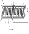
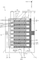
- FIG. 3 is a plan view in which the dielectric layer of the ozone generation element according to Embodiment 1 is omitted.
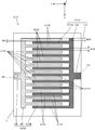
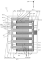
- 3 is a bottom view of the ozone generation element according to Embodiment 1.
- FIG. 6 is a plan view in which a dielectric layer of an ozone generating element according to Comparative Example 1 is omitted.
- FIG. It is the top view which abbreviate
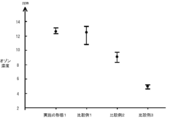
- FIG. It is a figure which shows the dispersion
- FIG. 6 is a schematic diagram of a part of an ozone generating element according to Comparative Example 1.
- FIG. 6 is an equivalent circuit diagram showing an ozone generation element according to Comparative Example 1.
- FIG. 2 is a schematic diagram of a part of the ozone generation element according to Embodiment 1.
- FIG. 3 is an equivalent circuit diagram illustrating the ozone generation element according to the first embodiment. According to the first embodiment, there are four electrode element groups of each electrode, and the distance between the terminal electrode part and the connecting part is the same as the distance between adjacent electrode element parts. It is the top view which omitted the body layer.
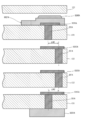
- FIG. 3 is a cross-sectional view taken along the line AA in FIG. 2 for explaining the method for manufacturing the element for generating ozone according to the first embodiment.
- FIG. 3 is a cross-sectional view taken along the line AA in FIG. 2 for explaining the method for manufacturing the element for generating ozone according to the first embodiment.
- FIG. 3 is a cross-sectional view taken along the line AA in FIG. 2 for explaining the method for manufacturing the element for generating ozone according to the first embodiment.
- FIG. 3 is a cross-sectional view taken along the line AA in FIG. 2 for explaining the method for manufacturing the element for generating ozone according to the first embodiment.
- FIG. 3 is a cross-sectional view taken along the line AA in FIG. 2 for explaining the method for manufacturing the element for generating ozone according to the first embodiment.
- FIG. 3 is a cross-sectional view taken along the line AA in FIG. 2 for explaining the method for manufacturing the element for generating ozone according to the first embodiment.
- FIG. 3 is a cross-sectional view taken along the line AA in FIG. 2 for explaining the method for manufacturing the element for generating ozone according to the first embodiment.
- 6 is a schematic diagram of a part of an ozone generation element according to Embodiment 2.
- FIG. 2 is a schematic diagram of a part of an ozone generation element according to Embodiment 2.
- FIG. 6 is an equivalent circuit diagram showing an ozone generation element according to Embodiment 2.
- FIG. according to the second embodiment there are three electrode element groups of each electrode, and the distance between the terminal electrode part and the connecting part is the same as the distance between adjacent electrode element parts. It is the top view which omitted the body layer.
- FIG. 9 is a plan view in which a dielectric layer of an ozone generation element according to Modification 1 is omitted.
- FIG. 10 is a plan view in which a dielectric layer of an ozone generation element according to Modification 2 is omitted.
- FIG. 10 is a plan view in which a dielectric layer of an ozone generation element according to Modification 3 is omitted.
- FIG. 10 is a plan view in which a dielectric layer of an ozone generation element according to Modification 4 is omitted.
- FIG. 10 is a plan view in which a dielectric layer of an ozone generation element according to Modification 5 is omitted.
- FIG. 10 is a plan view in which a dielectric layer of an ozone generation element according to Modification 6 is omitted.
- FIG. 20 is a cross-sectional view of the ozone generation element according to Modification 6 taken along line BB of FIG. 12 is a cross-sectional view for explaining a method for manufacturing an ozone generating element according to Modification 6.
- FIG. 20 is a cross-sectional view of the ozone generation element according to Modification 6
- the ozone generating apparatus includes an ozone generating element 10 and an AC power supply 31 that applies an AC voltage to the ozone generating element 10.
- the element for generating ozone 10 has a plate shape having a longitudinal direction and a transverse direction, and includes a dielectric substrate 13, a pair of electrodes 21A and 21B, a dielectric layer 12, back electrodes 25A and 25B, and filling. Vias 26A and 26B.
- the ozone generating element 10 is appropriately set in the Z direction, and the direction from the dielectric substrate 13 to the dielectric layer 12 in the Z direction is the + Z direction or upward, and the thickness direction of the ozone generating element 10 is The longitudinal direction of the ozone generating element 10 that is orthogonal to the X axis direction, the Z axis direction, and the short direction of the ozone generating element 10 that is orthogonal to the X axis direction will be described as the Y axis direction.
- the dielectric substrate 13 has a rectangular plate shape. Contact holes 131A and 131B penetrating the dielectric substrate 13 in the thickness direction are formed at both ends of the dielectric substrate 13 in the Y-axis direction in FIG. Conductive members are disposed in the contact holes 131A and 131B, respectively, to form filling vias 26A and 26B.
- the dielectric substrate 13 is made of a ceramic material containing an oxide such as CaO—B 2 O 3 —Al 2 O 3 —SiO 2 , Al 2 O 3 , SiO 2 , ZrO 2 , BaTiO 3 . Further, the dielectric substrate 13 may be formed of a LTCC (Low Temperature Co-fired Ceramics) substrate.
- the dielectric substrate 13 is not limited to a ceramic material as long as it has electrical insulation, and may be formed from a resin material such as an epoxy resin or a polyimide resin.
- the electrodes 21 ⁇ / b> A and 21 ⁇ / b> B are provided on the upper surface of the dielectric substrate 13.
- the pair of electrodes 21A and 21B includes an even number (16 in FIG. 2) of electrode parts 221A and 221B and a connecting part (first connecting part) that connects the plurality of electrode parts 221A. 222A, a connecting portion (first connecting portion) 222B for connecting the plurality of electrode portions 221B, terminal electrode portions 23A and 23B, and tongue pieces 24A and 24B.
- Electrodes 21A, 21B is, Cu, Ag, Pd, Pt , and is formed of a conductive oxide such as a metal or RuO 2 of W or the like.
- the electrodes 21A and 21B are made of metal, they can diffuse to the dielectric substrate 13 and the dielectric layer 12 during the baking process of the electrodes 21A and 21B. .
- the electrodes 21A and 21B are preferably made of a conductive oxide such as RuO2.
- the thickness of the electrodes 21A and 21B is set to about 10 ⁇ m.
- the electrodes 21A and 21B correspond to the first comb electrode and the second comb electrode of the present invention.
- the terminal electrode portion 23A corresponds to the first terminal electrode portion of the present invention, and the terminal electrode portion 23B corresponds to the second terminal electrode portion of the present invention.
- the electrode portions 221A and 221B are each formed in an elongated shape having a longitudinal direction and a short direction, and are arranged side by side in the X-axis direction with the longitudinal direction as the Y-axis direction.
- Electrode element sets 22A and 22B are composed of electrode element parts 221A and 221B, two electrode element parts 221A and 221B adjacent to electrode element parts 221A and 221B in the X-axis direction, and connecting parts 222A and 221B. .
- the electrode assembly 22A corresponds to the first electrode assembly of the present invention
- the electrode assembly 22B corresponds to the second electrode assembly of the present application. There are a plurality (eight in FIG.
- electrode element groups 22A and 22B are arranged side by side in the X-axis direction.
- the plurality of electrode element groups 22A and 22B have a comb shape together with the terminal electrode parts 23A and 23B.
- One electrode group 22B is arranged between two electrode groups 22A adjacent to each other in the X-axis direction, and two electrode groups 22B adjacent in the X-axis direction.
- One set of electrode element sets 22A is arranged between them. That is, the pair of electrodes 21A and 21B has a so-called interdigital structure in which the electrode element groups 22A and the electrode element groups 22B are alternately arranged in the X-axis direction.
- the connecting portion 222A extends in the X-axis direction, and is the same electrode portion as the end portion in the + Y direction (third direction) that is one side in the longitudinal direction of each electrode portion 221A constituting the electrode portion set 22A.
- the other electrode element 221A constituting the set 22A is connected to the + Y-direction end.
- the connecting portion 222B extends in the X-axis direction, and is the same as the end portion in the ⁇ Y direction (first direction) which is the other side in the longitudinal direction of each electrode element portion 221B constituting the electrode element set 22B.
- the other electrode element part 221B constituting the electrode element part set 22B is connected to the end part in the -Y direction.
- the line widths of the connecting portions 222A and 222B are equal to the line width W11 of the electrode portions 221A and 221B.
- the interval between the electrode element group 22B and the electrode element group 22A adjacent to the electrode element group 22B in the X-axis direction is defined as W14.
- W14 is the same as the line widths W11A and W11B of the electrode portions 221A and 221B, for example.
- the terminal electrode portion 23A extends in the X-axis direction, and is connected to an end portion in the ⁇ Y direction (first direction) of each electrode portion 221A constituting the electrode portion set 22A.
- the terminal electrode portion 23B extends in the X-axis direction and is connected to an end portion in the + Y direction (first direction) of each electrode element portion 221B constituting the electrode element portion set 22B.
- the distance (second distance) W12 is not less than the distance (first distance) W14. In addition, it is more preferable that the distance (second distance) W12 is longer than the distance (first distance) W14 because printing blur at the end in the + Y direction of the electrode portion 221A can be reduced.
- the distance W14 corresponds to the distance between the electrode element set 22A of the electrode 21A and the electrode element set 22B of the electrode 21B adjacent to the electrode element set 22A in the X-axis direction.
- the distance W12 corresponds to the distance between the end in the + Y direction of the electrode element 221A constituting the electrode element set 22A of the electrode 21A and the terminal electrode part 23B of the electrode 21B.
- the end portion in the ⁇ Y direction of the electrode element portion 221B constituting the electrode element portion set 22B of the electrode 21B is also arranged apart from the terminal electrode portion 23A of the electrode 21A.
- the distance (second distance) W13 is equal to or greater than the distance (first distance) W14. Note that it is more preferable that the distance (second distance) W13 is longer than the distance (first distance) W14 because printing blur at the end in the ⁇ Y direction of the electrode section 221B can be reduced.
- the distance W13 corresponds to the distance between the end portion in the ⁇ Y direction of the electrode portion 221B constituting the electrode portion set 22B of the electrode 21B and the terminal electrode portion 23A of the electrode 21A.
- the tongue piece portion 24A extends in the ⁇ Y direction from the central portion of the terminal electrode portion 23A in the X-axis direction.
- the tongue piece 24A is electrically connected to a filling via (first filling via) 26A.
- the tongue piece portion 24B extends in the + Y direction from the central portion of the terminal electrode portion 23B in the X-axis direction.
- the tongue piece 24B is electrically connected to a filling via (second filling via) 26B.
- the dielectric layer 12 covers the electrodes 21 ⁇ / b> A and 21 ⁇ / b> B provided on the upper surface of the dielectric substrate 13.
- the dielectric layer 12 is made of a ceramic material containing an oxide such as CaO—B 2 O 3 —Al 2 O 3 —SiO 2 , Al 2 O 3 , SiO 2 , ZrO 2 , BaTiO 3 .
- the dielectric layer 12 may be made of an LTCC material.
- the dielectric substrate 13 is not limited to a ceramic material as long as it has electrical insulation, and may be formed from a resin material such as an epoxy resin or a polyimide resin.
- the dielectric layer 12 becomes high temperature by being exposed to plasma.
- the dielectric layer 12 is exposed to ozone generated in the vicinity of the surface thereof, erosion resistance against ozone is also required.
- the dielectric layer 12 is preferably formed of a ceramic material.
- the dielectric layer 12 is preferably made of a material whose thermal expansion coefficient is substantially equal to the thermal expansion coefficient of the dielectric substrate 13. In this case, even when the dielectric substrate 13 and the dielectric layer 12 expand and contract due to the heat generated during the operation of the ozone generating element 10, the junction between the dielectric substrate 13 and the dielectric layer 12 is distorted. Is unlikely to occur.
- the dielectric layer 12 is more preferably formed from the same material as the dielectric substrate 13.
- the back electrodes 25A and 25B are provided so as to cover at least the contact holes 131A and 131B of the dielectric substrate 13 on the surface of the dielectric substrate 13 opposite to the dielectric layer 12 side. Yes.
- the electrode 21A is electrically connected to the back electrode 25A through the filling via 26A.
- the electrode 21B is electrically connected to the back electrode 25B through the filling via 26A.
- the back electrodes 25A and 25B and the filling vias 26A and 26B are made of a metal such as Cu, Ag, Pd, Pt, or W, or a conductive material such as RuO 2 .
- the AC power supply 31 is electrically connected to the back electrodes 25A and 25B, and applies an AC voltage (sine wave voltage) between the pair of electrodes 21A and 21B.
- the AC power supply 31 may apply a rectangular pulse train AC voltage between the electrodes 21A and 21B.
- the dielectric substrate 13 has a square shape of 10 mm ⁇ 10 mm in plan view, and the thickness of the dielectric layer 12 is 15 ⁇ m.
- the total thickness of the dielectric substrate 13 and the dielectric layer 12 was about 600 ⁇ m.
- the length L1 in the X-axis direction of the region where the portions excluding the tongue pieces 24A and 24B in the electrodes 21A and 21B on the dielectric substrate 13 are 6 mm, and the length L2 in the Y-axis direction is 3 mm.
- the ozone generating element 9110 has electrode elements 9122 ⁇ / b> A and 9122 ⁇ / b> B of electrodes 9121 ⁇ / b> A and 9121 ⁇ / b> B each having a single linear shape extending in the Y-axis direction.
- the intervals between the portions 9122A and 9122B are all set to the same distance W94.
- Line widths W91A and W91B of electrode portions 9122A and 9122B are equal.
- the ozone generation element 9110 an element in which the distances W91A and W91B were set to 50 ⁇ m and the distance W94 was set to 50 ⁇ m was prepared.
- the dimensions of the regions where 9122A and 9122B and the terminal electrode portions 23A and 23B are provided are the same as those of the ozone generating element 10.
- the ozone generating element 9210 according to Comparative Examples 2 and 3 is a single linear shape in which the electrode portions 9222A and 9222B of the electrodes 9221A and 9221B both extend in the Y-axis direction.
- the intervals between the electrode portions 9222A and 9222B are all set to the same distance W94.
- the line widths W92A and W92B of the electrode element portions 9222A and 9222B are set longer than the interval W94 between the adjacent electrode element portions 9222A and 9222B.
- the inventors conducted discharge start voltage measurement, discharge state observation, and ozone generation amount of the ozone generation elements 10, 9110, and 9210 for evaluating the discharge start voltage, discharge state, and ozone generation amount.
- the contents of the measurement will be described.
- application is performed between the pair of electrodes 21A and 21B of the ozone generation element 10, between the pair of electrodes 9121A and 9121B of the ozone generation element 9110, and between the pair of electrodes 9221A and 9221B of the ozone generation element 9210.
- the presence or absence of plasma emission generated by discharge was observed while gradually increasing the voltage amplitude value of the alternating voltage (sine wave voltage).
- the voltage amplitude value at the time when plasma emission was observed was taken as the discharge start voltage.
- 30 ozone generating elements 10 according to the embodiment, 30 ozone generating elements 9110 according to comparative example 1, and 30 ozone generating elements 9210 according to comparative examples 2 and 3 are prepared. Then, the discharge start voltage was measured for each as described above.
- the voltage amplitude is between the pair of electrodes 21A and 21B of the ozone generation element 10, between the pair of electrodes 9121A and 9121B of the ozone generation element 9110, and between the pair of electrodes 9221A and 9221B of the ozone generation element 9210.
- An AC voltage (sinusoidal voltage) having a value of 2.5 kV was applied for discharging.
- the ozone generation elements 10, 9110 and 9210 were viewed in plan, and the discharge state between the electrodes 21A and 21B, the electrodes 9121A and 9121B or the electrodes 9221A and 9221B was observed.
- the ozone generation element 10, 9110, 9210 is placed in an acrylic case having a volume of 7 liters, and the ozone generation element 10, 9110, 9210 is driven for 3 minutes.
- the ozone concentration was measured with an ozone densitometer.
- a voltage amplitude value 2 An AC voltage (sine wave voltage) of 0.5 kV was applied.
- a fan was provided in the acrylic case so that the gas in the acrylic case was stirred.
- model EG-3000 manufactured by Sugawara Jitsugyo Co., Ltd. was used for the ozone concentration meter.
- 30 ozone generating elements 10 according to the embodiment and 30 ozone generating elements 9110 and 9210 according to comparative examples 1, 2, and 3 were prepared, respectively, Thus, the ozone concentration was measured.
- FIG. 6A shows the result of measuring the variation (3 ⁇ ) in the discharge start voltage. As shown in FIG. 6A, the variation in the discharge start voltage of the ozone generation element 10 was smaller than the variation in the discharge start voltages of the ozone generation elements 9110 and 9210.
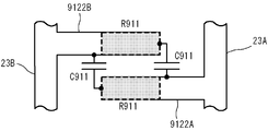
- discharge start portion the electrostatic capacity of the portion where discharge occurs first (hereinafter referred to as “discharge start portion”) is C911, the capacitance is between the terminal electrode portion 23A and the terminal electrode portion 23B. It can be considered that an equivalent circuit as shown in FIG. 7B is connected.
- R911 corresponds to a resistance component between the distal end portion of the electrode element portion 9122B and the terminal electrode portion 23B or a resistance component between the distal end portion of the electrode element portion 9122A and the terminal electrode portion 23A.
- the voltage VD91 applied to the discharge start portion of the ozone generating element 9110 is approximately represented by the following formula (1).
- VD91 VA ⁇ (R911 + ⁇ R911) ⁇ I (1)
- VA represents a voltage applied between the electrodes 9121A and 9121B
- I represents a current flowing through the electrode portions 9122A and 9122B at the start of discharge.
- the voltage VD91 indicates that a variation of about the voltage value obtained by multiplying the variation ⁇ R911 of the resistor R911 by the current value I occurs.
- the electrode assembly 22A, 22B has an equivalent circuit as shown in FIG. 7D connected between the terminal electrode portions 23A, 23B.
- R1 corresponds to a resistance component between the distal end portion of the electrode element portion 221B and the terminal electrode portion 23B or a resistance component between the distal end portion of the electrode element portion 221A and the terminal electrode portion 23A.
- the voltage VD1 applied to the discharge start portion of the ozone generating element 10 is approximately represented by the following formula (2).
- VD1 VA ⁇ (R1 + ⁇ R1) / 2 ⁇ I (2)
- VA represents a voltage applied between the electrodes 21A and 21B
- I represents a current flowing through the electrode portions 221A and 221B at the start of discharge.
- Equation (2) shows that the voltage VD1 has a variation of about the voltage value obtained by multiplying the half of the total of the resistance R1 and the variation ⁇ R1 by the current value I.
- the sum of the resistance R1 and the variation ⁇ R1 is equal to the sum of the resistance R911 and the variation ⁇ R911, and the current value I of the current flowing at the start of discharge is equal.
- the variation of the voltage VD1 is suppressed to about half of the variation of the voltage VD911.
- the ozone generating element 10 is compared with the ozone generating element 9110 to the voltage VD1 applied to the discharge start portion of the variation ⁇ R1 in the resistance R1 due to the variation in the line width W11 of the electrode portions 221A and 221B. The impact of has been reduced. Therefore, when the discharge between the electrode portions 221A and 221B starts, the variation in the discharge start voltage, which is the voltage applied between the electrodes 21A and 21B, is reduced.
- the disconnected electrode element 221A. 221B is also considered to contribute to the discharge generated between the electrode element groups 22A and 22B.
- the terminal electrode portions 23A and 23B and the disconnected electrode element portions 221A and 221B on the connecting portion 222A and 222B side are electrically connected via the other electrode element portions 221A and 221B and the connecting portions 222A and 222B. This is because the state connected to is maintained.
- FIG. 6B the measurement result of the ozone generation amount for the ozone generation elements 10, 9110 and 9210 is shown in FIG. 6B.
- the result was that the ozone concentration in the case of the ozone generation element 9210 according to Comparative Examples 2 and 3 was lower than the ozone concentration in the case of the ozone generation elements 10 and 9110.
- the result that the average value of the ozone concentration in the elements 10 and 9110 for ozone generation was substantially the same was obtained.
- the line width of the electrode portions 221A and 221B of the ozone generating element 10 or the electrode portions 9122A and 9122B of the ozone generating element 9110 is preferably 50 ⁇ m rather than 100 ⁇ m and 200 ⁇ m.
- the inventors relate to the ozone generation element 10 according to the present embodiment, the ozone generation element 9110 according to Comparative Example 1, and the Comparative Examples 2 and 3.
- the temperature at the start of discharge was measured.
- the ozone generation elements 10, 9110, and 9210 were operated with a thermocouple attached to the back surface of the ozone generation elements 10, 9110, and 9210.
- the operating temperature of the ozone generating element 10 was 70 ° C.
- the operating temperature of the ozone generating element 9110 was 65 ° C.
- the operating temperatures of the ozone generating element 9210 according to Comparative Examples 2 and 3 were 105 ° C. and 130 ° C., respectively. That is, the temperature during operation of the ozone generation element 9210 according to Comparative Examples 2 and 3 is compared with the temperature during operation of the ozone generation element 10 according to the present embodiment and the ozone generation element 9110 according to Comparative Example 1. It is hot. From these results and the property of ozone that ozone decomposition is promoted as the ambient temperature of ozone is higher, the ozone generating element 9210 according to Comparative Examples 2 and 3 is compared with the ozone generating elements 10 and 9110. It is considered that ozone decomposition in the vicinity of the ozone generating element 9210 was promoted, and as a result, the ozone concentration decreased.
- ozone generating elements according to the present embodiment ozone generating elements 510 and 610 as shown in FIGS. 8A and 8B were used.
- the evaluation of the discharge state was performed by observing the plasma emission generated by the discharge between all the electrode element groups 22A and 22B, as described above.
- the distance (first distance) W14 between the electrode element set 22A and the adjacent electrode element set 22B is the terminal electrode of the electrode element 221A of the electrode 21A.
- the distance (second distance) W12 between the end portion in the direction opposite to the portion 23A and the terminal electrode portion 23B is equal.
- the distance W14 is also equal to the distance (second distance) W13 between the end of the electrode element 221B of the electrode 21B in the direction opposite to the terminal electrode portion 23B and the terminal electrode portion 23A.
- the distance W14 is shorter than the distance W12 and the distance W13.
- the ozone generating element 510 actually used for evaluating the discharge state has distances W14, W12, and W13 of 50 ⁇ m. Further, the ozone generating element 610 actually used for evaluating the discharge state has a distance W14 of 50 ⁇ m, and distances W12 and W13 of 200 ⁇ m and 800 ⁇ m.
- 50 ozone generation elements 510, 610, and 9110 were prepared, respectively, and the discharge state was evaluated.
- an AC sine wave having a voltage amplitude value of 3.0 kV and 30 kHz is applied between the pair of electrodes 21A and 21B of the ozone generation elements 510 and 610 and between the pair of electrodes 9121A and 9121B of the ozone generation element 9110.
- the ON / OFF time setting of the applied voltage was set to the following cycle (duty ratio).
- Period 50 sec and ON time 5 sec (duty ratio 10%)
- Period 20 sec and ON time 3 sec (duty ratio 15%)
- Period 5 sec and ON time 1 sec (duty ratio 20%)
- Period 10 sec and ON time 1 sec (duty ratio 10%)
- the longer the on-time the easier the discharge occurs.
- discharge is most likely to occur when a voltage is applied with an on time of 5 sec, and when a voltage with an on time of 3 sec is applied, discharge is less likely to occur in the order in which a voltage with an on time of 1 sec is applied. Further, if the on-time is the same, the shorter the off-time, the easier the discharge occurs. This is because the electrodes 21A and 21B are cooled correspondingly as the off-time becomes longer. When the temperature of the electrodes 21A and 21B is lowered, the kinetic energy of electrons existing in the vicinity of the electrodes 21A and 21B when a voltage is applied between the electrodes 21A and 21B is reduced, so that discharge is less likely to occur. It is. Therefore, when a voltage having a period of 10 sec and an on time of 1 sec is applied, discharge is less likely to occur than when a voltage having a period of 5 sec and an on time of 1 sec is applied.
- Table 1 below shows the results of the evaluation of the discharge state of the ozone generation elements 510, 610, and 9110.
- period indicates the period of the voltage ON / OFF time
- Ton indicates the time during which the AC voltage is applied between the electrodes 21A and 21B in one period.
- Toff indicates an off time which is a time during which the AC voltage is not applied between the electrodes 21A and 21B in one cycle.
- Duty ratio indicates a ratio of on time (on duty) in one cycle of ON / OFF time setting of AC voltage.
- “ ⁇ ” indicates that plasma emission was observed between all electrode element groups 22A and 22B, and “ ⁇ ” indicates that plasma emission was observed between some electrode element groups 22A and 22B. Indicates. Further, “x” indicates that plasma emission was not observed between all the electrode element groups 22A and 22B.
- the ozone generating element 9110 according to Comparative Example 1 is discharged for all the evaluation samples. Did not occur. In other words, in the ozone generation element 9110, no discharge occurred during the period from when the voltage application between the electrodes 21A and 21B was started until the ON time of 1 to 5 seconds had elapsed.
- the ozone generating elements 510 and 610 according to the present embodiment discharge all of the evaluation samples when AC voltage is repeatedly applied with a period of 20 to 50 sec and an on-time of 3 to 5 sec. Occurred.
- the ozone generation elements 510 and 610 discharge was generated after the voltage application between the electrodes 21A and 21B was started and before the on-time (1 to 5 seconds) passed. From these facts, the ozone generation elements 510 and 610 are compared with the ozone generation element 9110 according to Comparative Example 1 in the time from when the voltage application between the electrodes 21A and 21B is started until the discharge is generated. You can see it is short. That is, the ozone generating elements 510 and 610 are superior to the ozone generating element 9110 according to the comparative example 1 in response to voltage application between the electrodes 21A and 21B.
- the ozone generating element 510 when the AC voltage was repeatedly applied to the ozone generating element 610 with a period of 5 to 10 sec and an ON time per period of 1 sec, no discharge occurred in all the samples for evaluation.
- the ozone generating element 510 when an AC voltage having a cycle of 5 to 10 seconds and an ON time per cycle of 1 sec was repeatedly applied, discharge was generated for all the samples for evaluation. From this, it can be seen that the ozone generating element 510 is shorter than the ozone generating element 610 in the time from when the voltage application is started between the electrodes 21A and 21B until the discharge is generated. That is, the ozone generating element 510 is more excellent in response to voltage application between the electrodes 21A and 21B than the ozone generating element 610.
- the reason for the difference in response between the ozone generating elements 510 and 610 is considered as follows.
- the distances W12 and W13 are set longer than the distance W14.
- the discharge between the electrode element set 22A and the terminal electrode part 23B and between the electrode element set 22B and the terminal electrode part 23A are unlikely to occur, and the responsiveness decreases accordingly.
- the distances W12 and W13 are equal to the distance W14.
- electric discharge is likely to occur between the electrode element group 22A and the terminal electrode part 23B and between the electrode element group 22B and the terminal electrode part 23A, and the responsiveness is improved accordingly.
- FIGS. 9A, 9B, 9C, 9D, 10A, and 10B are cross-sectional views at each step corresponding to the cross-sectional view of the ozone generation element 10 along the line AA in FIG. .
- this manufacturing method first, a dielectric sheet serving as a base for the dielectric substrate 13 and the dielectric layer 12 is formed, and then a metal paste pattern serving as a base for the electrodes 21A, 21B and the like is formed on the dielectric sheet. Then, after laminating dielectric sheets, the laminated body of dielectric sheets is fired to produce the ozone generating element 10.
- a dielectric sheet (so-called ceramic green sheet) that forms the basis of the dielectric substrate 13 and the dielectric layer 12 is formed.
- a CaO—B 2 O 3 —Al 2 O 3 —SiO 2 glass, a mixed solvent of Al 2 O 3 , toluene and ethanol, a dispersant, a binder, and a ball mill are used.
- a slurry is prepared by pulverizing and mixing.
- a dielectric sheet is produced from the obtained slurry by a doctor blade method.
- the material used in the sheet forming step is not limited to the one containing the above-mentioned materials, but other types of glass other than CaO—B 2 O 3 —Al 2 O 3 —SiO 2 glass or SiO 2 , ZrO 2 , BaTiO 3 and other oxides may be included.
- a resin material such as an epoxy resin or a polyimide resin
- a resin material such as an epoxy resin or a polyimide resin may be used in the sheet forming step.
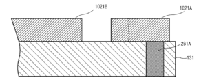
- a metal paste filling portion serving as a basis for the filling vias 26A and 26B is formed in the plurality of dielectric sheets used for the dielectric substrate 13. Specifically, first, as shown in FIG. 9A, through holes 132A penetrating in the thickness direction are formed in each dielectric sheet 131 using a punching device such as a mechanical puncher. The through holes 132A are formed so as to be relatively at the same position when the dielectric sheets 131 are laminated. Next, as shown in FIG. 9B, Ag paste is filled in each through-hole 132A of the dielectric sheet 131. Thereby, the metal paste filling portion 261A is formed in the dielectric sheet 131.
- first metal paste patterns 1021A and 1021B that form the basis of the electrodes 21A and 21B are formed on the dielectric sheet disposed on the uppermost layer of the dielectric substrate 13 as shown in FIG. 9C.
- the back electrode 25A is applied to the dielectric sheet 131 disposed in the lowermost layer of the dielectric substrate 13 among the plurality of dielectric sheets used for the dielectric substrate 13 as shown in FIG. 9D.
- 25B to form a second metal paste pattern 251A.
- the first metal paste patterns 1021A and 1021B and the second metal paste pattern 251A are made of RuO 2 paste.
- a plurality of dielectric sheets 131 are laminated, and one dielectric sheet 121 serving as a base of the dielectric layer 12 is laminated on the dielectric sheet 131 disposed at the top.
- the dielectric sheets 121 and 131 are crimped by a crimping machine to obtain a laminate.
- the obtained laminate is fired at a firing temperature of 900 ° C.
- the dielectric sheets 121 and 131 are sintered to form the dielectric layers 12 and 132.
- the metal paste filling portion 261A, the first metal paste patterns 1021A and 1021B, and the second metal paste pattern 251A are sintered to form the filling vias 26A, the electrodes 21A and 21B, and the back electrode 25A.
- This manufacturing method of the ozone generating element 10 requires only one firing process which is relatively laborious compared to other processes. Therefore, there is an advantage that the burden on the worker who is engaged in manufacturing the ozone generating element 10 is reduced.
- the electrode portions 9122A and 9122B where the disconnection has occurred do not contribute to the discharge, and the amount of ozone generated in the ozone generating element 9110 is reduced by 10% or more. Therefore, it is necessary to sort out such an ozone generating element 9110 as a defective product so that it does not flow out to the market. As a measure for this, it may be possible to introduce a pre-shipment inspection step for inspecting the discharge state of the ozone generating element 9110 before the shipment. However, when such a pre-shipment inspection process is introduced, the burden on the operator who manufactures the element 9110 for ozone generation increases. Moreover, when it determines with a defect in the stage of a pre-shipment inspection, the whole module in which the element 9110 for ozone production
- the ozone generating element 10 even if a disconnection occurs in the two electrode parts 221A and 221B due to a manufacturing defect or the like, The state of being electrically connected to the terminal electrode portions 23A and 23B via the electrode portions 221A and 221B and the connecting portions 222A and 222B is maintained. Thereby, since the disconnected electrode element portions 221A and 221B contribute to the discharge generated between the electrode element group sets 22A and 22B, a decrease in the amount of ozone generated in the ozone generation element 10 due to the disconnection is suppressed.
- the number of ozone generating elements 10 selected as defective products due to the disconnection of the electrode portions 221A and 221B is reduced. If the defect rate of the ozone generating element 10 can be reduced to an allowable range that does not require the pre-shipment inspection process of the ozone generating element 10, the burden on the operator can be reduced and the manufacturing cost can be reduced. Is also planned.
- the ozone generation element 10 according to the present embodiment has a larger amount of ozone generation than the ozone generation element 9210 according to Comparative Examples 2 and 3. That is, even if the ozone generating element 10 is not cooled, it can generate the same amount of ozone as the ozone generating element 9210 that operates while being cooled by the cooling mechanism. In addition, the rate of occurrence of a portion that does not discharge due to the disconnection of the electrode portions 221A and 221B is equal to that of the ozone generating element 9210. That is, the ozone generating element 10 according to the present embodiment can have the same performance as the ozone generating element 9210 that operates while being cooled without being cooled by the cooling mechanism. A small module including the ozone generating element 10 can be realized.
- the dielectric layer 12 covers one surface of the dielectric substrate 13 on which the electrodes 21A and 21B are formed.
- the distance W14 is equal to or less than the distances W12 and W13. Accordingly, as compared with the ozone generating element 9110 according to Comparative Example 1, there is an advantage that the time from when the voltage application is started between the electrodes 21A and 21B until the discharge is generated is short and the response is excellent.
- the ozone generating element 2010 is different from the ozone generating element 10 according to the first embodiment in the shape of the electrodes.
- the ozone generating element 2010 according to the present embodiment includes a dielectric substrate 13, a pair of electrodes 2021A and 2021B, filling vias 26A and 26B, and a pair of backside electrodes (not shown). And comprising.
- this ozone generation element 2010 is also used in a state in which an AC power source is connected to a pair of back surface electrodes.
- the same components as those in the first embodiment are denoted by the same reference numerals.
- the ozone generation element 2010 includes the dielectric layer 12 and the back surface electrodes 25 ⁇ / b> A and 25 ⁇ / b> B as described in Embodiment 1 with reference to FIGS. 1 and 3.
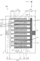
- the pair of electrodes 2021A and 2021B includes a plurality (16 pieces in FIG. 11) of electrode element portions 2221A and 2221B, terminal electrode portions 2023A and 2023B, and connection portions 2222A, 2222B, 2027A and 2027B. And tongue pieces 24A and 24B.
- the electrodes 2021A and 2021B correspond to the first comb electrode and the second comb electrode of the present invention.
- the terminal electrode portion 2023A corresponds to the first terminal electrode portion of the present invention, and the terminal electrode portion 2023B corresponds to the second terminal electrode portion of the present invention.
- the electrode portions 2221A and 2221B are elongated shapes each having a longitudinal direction and a lateral direction, and are arranged in the X-axis direction with the longitudinal direction as the Y-axis direction.
- the electrode element portions 2221A and 2221B, two electrode element portions 2221A and 2221B adjacent in the X-axis direction, and connecting portions 2222A, 2222B, 2027A and 2027B constitute electrode element portion sets 2022A and 2022B.
- the electrode assembly 2022A corresponds to the first electrode assembly of the present invention
- the electrode assembly 2022B corresponds to the second electrode assembly of the present invention. There are a plurality (eight in FIG.
- electrode element groups 2022A and 2022B are arranged side by side in the X-axis direction.
- One electrode group 2022B is arranged between two electrode groups 2022A adjacent to each other in the X-axis direction 2022A, and two electrode groups 2022B adjacent to each other in the X-axis direction.
- One set of electrode parts 2022A is disposed between them.
- connection part (first connection part) 2222A is the same electrode element part set 2022A as the end part in the + Y direction (third direction) which is one side in the longitudinal direction of each electrode element part 2221A constituting the electrode element part set 2022A. Are connected to the end in the + Y direction of the other electrode element portion 2221A.
- the connecting portion 2222B is connected to the end in the ⁇ Y direction (first direction), which is the other side in the longitudinal direction of each electrode portion 2221B constituting the electrode portion set 2022B, and the other ends constituting the same electrode portion set 2022B. The end of the electrode portion 2221B in the ⁇ Y direction is connected.
- the line widths of the connecting portions 2222A and 2222B are equal to the line widths W11A and W11B of the electrode portions 2221A and 2221B. Note that an interval between the electrode element group 2022B and the electrode element group 2022A adjacent to the electrode element group 2022B in the X-axis direction is defined as W14. W14 is all set to the same distance as the line widths W11A and W11B of the electrode portions 2221A and 2221B.
- the connecting portion (second connecting portion) 2027A is in contact with the electrode portion 2221A in the + X direction (second direction) that is one side in the short direction or the ⁇ X direction (fourth direction) that is the other side in the short direction.
- the electrode part 2221A that constitutes another adjacent electrode element part set 2022A is connected.
- the other electrode element group 2022A corresponds to the remaining electrode element group 2022A excluding two electrode element groups 2022A located at both ends in the X-axis direction among the plurality of electrode element groups 2022A.
- the connecting portion (second connecting portion) 2027B includes another electrode element adjacent to the electrode portion 2221B constituting the electrode portion set 2022B in the + X direction (second direction) or the ⁇ X direction (fourth direction).
- the electrode part 2221B which constitutes the part set 2022B is connected.
- the other electrode element group 2022B corresponds to the remaining electrode element group 2022B excluding two electrode element groups 2022B located at both ends in the X-axis direction among the plurality of electrode element groups 2022B.
- the line widths of the connecting portions 2027A and 2027B are equal to the line widths W11A and W11B of the electrode portions 2221A and 2221B.
- the terminal electrode portions 2023A and 2023B have an elongated shape having a longitudinal direction and a lateral direction, and extend in the X-axis direction.
- the terminal electrode portion 2023A includes an electrode portion 2221A constituting the electrode portion set 2022A located at the end in the + X direction (second direction) of the plurality of electrode portion sets 2022A and the ⁇ X direction (fourth direction). It is connected to the electrode part 2221A constituting the electrode part set 2022A located at the end.
- the terminal electrode portion 2023B is connected to the electrode portion 2221B constituting the electrode portion set 2022B located at the end in the + X direction (second direction) of the plurality of electrode portion sets 2022B in the ⁇ X direction (fourth direction).
- both end portions in the X-axis direction of the terminal electrode portion 2023A are respectively connected to electrode portions 2221A located at both ends in the X-axis direction among the plurality of electrode portions 2221A.
- both end portions in the X-axis direction of the terminal electrode portion 2023B are connected to electrode portions 2221B located at both ends in the X-axis direction among the plurality of electrode portions 2221B, respectively.
- the ozone generation element 2010 according to the present embodiment will be described in comparison with the above-described comparative example 1.
- the results of measurement of the discharge start voltage, observation of the discharge state, and measurement of the amount of ozone generated will be described.
- the ozone generation element 2010 according to the present embodiment an element in which the distances W11A, W11B, and W14 in FIG. 11 were set to 50 ⁇ m was prepared.
- the shape of the dielectric substrate 13 is the same as that of the ozone generating element 10 according to the present embodiment.
- the length L21 in the X-axis direction of the region where the portions excluding the tongue pieces 24A and 24B in the electrodes 21A and 21B on the dielectric substrate 13 are provided is 6 mm, and the length L22 in the Y-axis direction is 3 mm.
- the measurement of the discharge start voltage and the observation of the discharge state were performed by the same method and the same conditions as the discharge start voltage measurement described in the first embodiment.
- the discharge start voltage of the ozone generating element 2010 according to the present embodiment was 2.5 kV.
- the variation (3 ⁇ ) in the discharge start voltage of the ozone generation element 2010 according to the present embodiment was 0.27 kV. That is, the result that the variation in the discharge start voltage of the ozone generation element 2010 according to the present embodiment is smaller than the variation in the discharge start voltages in Comparative Examples 1, 2, and 3 described in the first embodiment is obtained. It was. Further, in the observation of the discharge state, plasma emission generated by the discharge was observed between all the electrode portions 2221A and 2221B of the ozone generation element 2010 according to the present embodiment.
- the measurement of the ozone generation amount was also performed by the same method and the same conditions as the measurement of the ozone generation amount described in the first embodiment.
- the ozone concentration generated by the ozone generation element 2010 according to the present embodiment was substantially the same as that of the first embodiment.
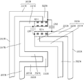
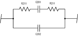
- the ozone generation element 2010 according to the present embodiment when discharge first occurs between the electrode element groups 2022A and 2022B arranged at both ends in the X-axis direction among the plurality of electrode element groups 2022A and 2022B. Conceivable. As shown in FIG. 12A, the electrode element groups 2022A and 2022B arranged at the end in the ⁇ X direction are defined between the terminal electrode parts 2023A and 2023B, assuming that the electrostatic capacity of the portion where discharge easily occurs is C201 and C202.
- R211 corresponds to the resistance component of the electrode portion 2221B or the electrode portion 2221A. Therefore, in the case of the ozone generation element 2010 according to the present embodiment, the discharge generated between the electrode element portions 2221A and 2221B continuous to the terminal electrode portions 2023A and 2023B is not affected by the variation of the resistance R211. That is, the discharge start voltage between the electrode portions 2221A and 2221B continuous to the terminal electrode portions 2023A and 2023B is substantially constant regardless of the variation in the resistance R211.
- Ozone generating elements 2510 and 2610 as shown in FIGS. 13A and 13B were used as the ozone generating elements according to the present embodiment.
- the ozone generating element 9110 according to Comparative Example 1 is the same as the ozone generating element 9110 described in the first embodiment.
- the evaluation of the discharge state was performed by the same method as in the first embodiment. In the element 2510 for ozone generation, as shown in FIG.
- the distance (third distance) W14 between the electrode assembly 2022A and the electrode assembly 2022B adjacent to each other is the connecting portion 2027A of the electrode assembly 2022A.
- the terminal electrode portion 2023A are equal to a distance (fourth distance) W23.
- the distance W14 is equal to the distance W22 between the connecting portion 2027B and the terminal electrode portion 2023B of the electrode element group 2022B.
- the distance W14 is equal to the distance (fifth distance) W13 between the connecting portion 2027A of the electrode element set 2022A and the connecting portion 2222B of the electrode element set 2022B.
- the distance W14 is equal to the distance W12 between the connecting portion 2027B of the electrode element set 2022B and the connecting portion 2222A of the electrode element set 2022A.
- the distance W14 is shorter than the distance W23 between the connecting portion 2027A of the electrode assembly 2022A and the terminal electrode portion 2023A.
- the distance W14 is shorter than the distance W22 between the connecting portion 2027B and the terminal electrode portion 2023B of the electrode assembly 2022B.
- the distance W14 is equal to the distance W13 between the connecting portion 2027A of the electrode element set 2022A and the connecting portion 2222B of the electrode element set 2022B.
- the distance W14 is equal to the distance W12 between the connecting portion 2027B of the electrode element set 2022B and the connecting portion 2222A of the electrode element set 2022A.
- the ozone generating elements 2510 and 2610 actually used for evaluating the discharge state have distances W12, W13, and W14 of 50 ⁇ m, and distances W22 and W23 of 200 ⁇ m and 800 ⁇ m.
- 50 ozone generating elements 2510, 2610, and 9110 were prepared, respectively, and the discharge state was evaluated.
- an alternating current sine wave having a voltage amplitude value of 3.0 kV is applied between the electrodes 2021A and 2021B of the ozone generation elements 2510 and 2610 and between the pair of electrodes 9121A and 9121B of the ozone generation element 9110.
- the ON / OFF time of the AC voltage is set such that the cycle is 50 sec and the on time is 5 sec (duty ratio 10%), the cycle 20 sec and the on time 3 sec (duty ratio 15%), the cycle 5 sec and the on time 1 sec (duty ratio 20). %), A period of 10 sec and an on-time of 1 sec (duty ratio 10%).
- the ozone generation elements 2510 and 2610 are all evaluated samples when an AC voltage having a cycle of 5 to 50 sec and an on-time of 1 to 5 sec per cycle is repeatedly applied. Discharge occurred.
- the ozone generation elements 2510 and 2610 discharge was generated after the on-time of 1 to 5 seconds had elapsed after the voltage application between the electrodes 2021A and 2021B was started.
- the ozone generation elements 2510 and 2610 have a shorter time from when the voltage application between the electrodes 2021A and 2021B is started to when the discharge occurs compared to the ozone generation element 9110 according to Comparative Example 1. I understand that. That is, the ozone generating elements 2510 and 2610 are more responsive to voltage application between the electrodes 2021A and 2021B than the ozone generating element 9110 according to Comparative Example 1.
- the ozone generation element 2610 when the ozone generation element 2610 repeatedly applies an AC voltage having a cycle of 10 sec and an on-time of 1 sec per cycle, the discharge is generated only between some electrode element groups 2022A and 2022B for all the samples for evaluation. occured.
- the ozone generation element 2510 when the ozone generation element 2510 repeatedly applies an AC voltage with a period of 10 sec and an on-time of 1 sec per period, discharge is performed between all electrode element groups 2022A and 2022B for all the evaluation samples. Occurred. From this, it can be seen that the ozone generating element 2510 is more excellent in responsiveness to voltage application between the electrodes 2021A and 2021B than the ozone generating element 2610. The discharge element discharges between the electrode unit groups having the shortest distance.
- the distance W22 is preferably larger than the distance W12.
- discharge is performed in the electrode element groups 2022A and 2022B arranged at both ends in the X-axis direction among the plurality of electrode element groups 2022A and 2022B. Since the variation in the start voltage is reduced, the variation in the amount of ozone generated can be suppressed more than in the first embodiment.
- the ozone generation element 2010 causes the disconnected electrode portion 2221A and the electrode portion 2221B to contribute to the discharge generated between the electrode portion sets 2022A and 2022B. be able to. Therefore, a decrease in the amount of ozone generated in the ozone generation element 2010 due to disconnection of the electrode portions 2221A and 2221B is suppressed.
- the element 2610 for ozone generation has all electrode parts when an AC voltage is applied with a period of 10 sec and an on-time per period of 1 sec, that is, even under conditions where discharge is hardly generated.
- a discharge can be generated between the sets 2022A and 2022B.
- the concentration of ozone generated by the ozone generating element 2610 can be controlled with high accuracy by the duty ratio of the voltage ON / OFF time applied between the electrodes 2021A and 2021B of the ozone generating element 2610. .
- the number of electrode parts constituting one electrode part group may be N (N is an integer of 3 or more).
- the electrode has multiple electrode sections that are N (N is an integer of 4 or more).
- the electrode 3021A and the electrode 3021B each have a multiple of three electrode parts 221A and 221B, and are adjacent in the X-axis direction.
- One electrode element set 3022A, 3022B may be configured from the three electrode element portions 221A, 221B.
- the same reference numerals as those in FIG. 2 are assigned to the same configurations as those in the first embodiment.
- the ends in the + Y direction of the three electrode elements 221A constituting the electrode element set 3022A are connected via a connecting part 3222A extending in the X-axis direction. Further, the ends in the ⁇ Y direction of the three electrode elements 221B constituting the electrode element set 3022B are also connected through a connecting part 3222B extending in the X-axis direction.
- any two of the three electrode parts 221A or the electrode elements 221B constituting the electrode element set 3022A or the electrode element set 3022B are disconnected due to a manufacturing defect or the like.
- the portion ahead of the location where the electrode portions 221A and 221B are disconnected is connected to the terminal electrode portions 23A and 23B via the remaining electrode portions 221A and 221B and the connecting portions 3222A and 3222B. And are electrically connected. Accordingly, since the disconnected electrode parts 221A and 221B can also contribute to the discharge between the electrode part groups 3022A and 3022B, the amount of ozone generated in the ozone generating element 3010 due to the disconnection of the electrode parts 221A and 221B Is reduced.
- the connecting portion 222A connects the ends in the + Y direction of the two electrode element portions 221A constituting the electrode element set 22A, and the connecting portion 222B constitutes the electrode element set 22B.
- the example in which the ends in the -Y direction of the two electrode portions 221B are connected has been described.
- the places where the connecting portions 222A and 222B connect the two electrode element portions 221A and 221B that constitute the electrode element group sets 22A and 22B are not limited to the ends of the electrode element portions 221A and 221B.
- the connecting portions 4222A and 4222B are other than the end portions of the two electrode element portions 221A and 221B constituting the electrode element portion sets 22A and 22B.
- the parts may be connected to each other.
- the same reference numerals as those in FIG. the same reference numerals as those in FIG.
- the connecting parts 4222A and 4222B connect the parts closer to the tip than the center parts of the two electrode parts 221A and 221B. It is not limited.
- the connecting portions 4222A and 4222B may connect the center portions of the two electrode element portions 221A and 221B or the portions closer to the base end portion than the center portions.
- This configuration can appropriately set the connecting position of the two electrode portions 221A and 221B by the connecting portions 4222A and 4222B according to the specifications of the manufacturing equipment of the ozone generating element 4010, for example.
- the example in which the two electrode elements 221A and 221B constituting the electrode element groups 22A and 22B are connected by one connecting part 222A and 222B has been described.
- the number of connecting portions 222A and 222B that connect the two electrode element portions 221A and 221B constituting the electrode element set 22A and 22B is not limited to one.
- two electrode element portions 221A and 221B constituting the electrode element group sets 22A and 22B are connected by three connection portions 5222A and 5222B. It may be.
- the two electrode element portions 221A and 221B constituting the electrode element group 22A and 22B When one of the two electrode element portions 221A and 221B constituting the electrode element group 22A and 22B is disconnected due to a manufacturing defect or the like, the two positions between the three connecting portions 5222A and 5222B are disconnected. To do. Even in this case, according to the present configuration, the three divided portions of the electrode portions 221A and 221B disconnected from the terminal electrode portions 23A and 23B are the remaining one electrode portion 221A and 221B and the connecting portion 5222A, The state of being electrically connected via 5222B is maintained.
- the disconnected electrode element portions 221A and 221B can also contribute to the discharge between the electrode element portion groups 3022A and 3022B, the amount of ozone generated in the ozone generating element 5010 due to the disconnection of the electrode element portions 221A and 221B Is reduced.
- the example in which the two electrode element portions 2221A and 2221B constituting the electrode element group sets 22A and 22B are connected by the three connection portions 5222A and 5222B has been described.
- the number of is not limited to three.
- the two electrode element parts 221A and 221B constituting the electrode element part sets 22A and 22B may be connected by four or more connecting parts, or may be connected by two connecting parts.
- the present invention is not limited to this, as in the ozone generation element 6010 according to Modification 4 shown in FIG. 17, the + Y direction or the ⁇ Y direction of the two electrode element parts 2221A and 2221B constituting the same electrode element part set 2022A and 2022B.
- the ends in the Y direction may be connected by connecting portions 2222A and 2222B, and the ends in the ⁇ Y direction and + Y direction may be connected by connecting portions 6028A and 6028B.
- a plurality of connecting portions 2222A and 2222B that connect ends in the + Y direction or ⁇ Y direction of two electrode element portions 2221A and 2221B constituting the electrode element sets 2022A and 2022B are disconnected. Even so, all the electrode element groups 2022A and 2022B can contribute to the discharge. Accordingly, a decrease in the amount of ozone generated in the ozone generating element 6010 due to the disconnection of the connecting portions 2222A and 2222B is suppressed.
- both end portions of the terminal electrode portion 2023A are positioned at both ends in the X-axis direction of the plurality of electrode portion sets 7022A.
- the both ends of the terminal electrode part 2023B may be connected to the electrode part set 7022B located at both ends in the X-axis direction of the plurality of electrode part sets 7022B.
- the ends in the + Y direction of the three electrode elements 2221A constituting the electrode element set 7022A are connected by a connecting part 7222A.
- the two electrode element parts 2221A in the ⁇ X direction are connected.
- the ends in the ⁇ Y direction are connected by a connecting portion 7028A.
- the ends in the ⁇ Y direction of the two electrode elements 2221A in the + X direction among the three electrode elements 2221A are not connected to each other.
- the ends in the ⁇ Y direction of the three electrode elements 2221B constituting the electrode element set 7022B are connected by a connecting part 7222B, and two electrode element parts in the + X direction of the three electrode element parts 2221B are connected.
- the ends in the + Y direction of 2221B are connected by a connecting portion 7028B.
- the ends in the + Y direction of the two electrode elements 2221B in the ⁇ X direction among the three electrode elements 2221B are not connected to each other.
- the dielectric substrate 13 and the dielectric layer 12 are formed from materials having substantially the same thermal expansion coefficient.
- the present invention is not limited thereto, and the dielectric substrate 13 and the dielectric layer 12 are You may form from the material from which a thermal expansion coefficient differs.
- the configuration including the dielectric layer 12 has been described.
- the configuration is not limited thereto, and a configuration without the dielectric layer 12 may be used.
- the configuration in which the AC power supply 31 is electrically connected to the back electrodes 25A and 25B has been described.
- the configuration is not limited thereto, and the AC power supply 31 is not the back electrodes 25A and 25B, but the dielectric substrate 13. It may be configured to be electrically connected to a part of the electrodes 21A and 21B (for example, tongue pieces 24A and 24B) provided on the surface of the electrode.
- the present invention is not limited thereto, and for example, the electrodes 21A and 21B are connected via the filling vias. It may be configured to be connected to an extraction electrode (not shown) provided on the end face of the dielectric substrate 13.
- the terminal electrode portions 23A and 23B are connected to the respective one filling vias 26A and 26B via the respective tongue pieces 24A and 24B
- the number of filling vias is one. It is not limited to.
- the terminal electrode portions 8023A and 8023B of the electrodes 8021A and 8021B are connected to the filling vias 8026A and 8026B via the two land portions 8024A and 8024B, respectively. It may be configured to be connected.
- An ozone generating element 8010 includes a dielectric substrate 8013, a pair of electrodes 8021A and 8021B, a filling via 8026A, a filling via 8026B, buffer portions 8266A and 8266B, and a pair of back electrodes (not shown). And). Similarly to the ozone generation element 2010 according to the second embodiment, this ozone generation element 8010 is also used in a state where an AC power source is connected to a pair of back surface electrodes. In FIG. 19, the same reference numerals as those in FIG. 11 are given to the same configurations as those in the second embodiment.
- the electrodes 8021A and 8021B include a plurality (16 pieces in FIG. 19) of electrode element portions 2221A and 2221B, connection portions 2222A, 2222B, 2027A and 2027B, Have
- the ozone generation element 8010 is provided with a dielectric layer 8012 so as to cover the main surface of the dielectric substrate 8013 on the side where the electrode 8021A is provided.
- the thickness of the dielectric layer 8012 is set to 25 ⁇ m, for example.
- the terminal electrode portion 8023A has two sub-terminal electrode portions 8231A and 8232A.
- the sub-terminal electrode part (first sub-terminal electrode part) 8231A is an electrode element part 2221A on the ⁇ X direction side that constitutes an electrode element part set 2022A located at the end in the ⁇ X direction of the plurality of electrode element sets 2022A. It is connected to the.
- the sub terminal electrode portion (second sub terminal electrode portion) 8232A is connected to the electrode portion 2221A on the + X direction side that constitutes the electrode portion set 2022A located at the end in the + Y direction among the plurality of electrode portion sets 2022A. Has been.
- the terminal electrode portion 8023B also includes two sub terminal electrode portions 8231B and 8232B.
- the sub terminal electrode part (third sub terminal electrode part) 8231B is connected to the electrode part 2221B on the + X direction side constituting the electrode part part set 2022B located at the end in the + X direction among the plurality of electrode part sets 2022B.
- the sub-terminal electrode portion (fourth sub-terminal electrode portion) 8232B is an electrode portion 2221B on the ⁇ X direction side that constitutes an electrode portion set 2022B located at the end in the ⁇ X direction of the plurality of electrode portion sets 2022B. It is connected to the.
- the sub terminal electrode portions 8231A and 8232A are electrically connected to a filling via (first filling via) 8026A via a land portion (first connection electrode portion) 8024A provided on the dielectric substrate 8013, respectively. .
- the sub terminal electrode portions 8231B and 8232B are electrically connected to a filling via (second filling via) 8026B via a land portion (second connection electrode portion) 8024B provided on the dielectric substrate 8013, respectively.
- the land portion 8024A is electrically connected to the back surface electrode 8025A at two locations on the dielectric substrate 8013 through the filling via 8026A.
- the land portion 8024B is electrically connected to the back surface electrode 8025B at two locations on the dielectric substrate 8013 through the filling via 8026B.
- the dielectric substrate 8013 is formed by laminating a plurality of (four in FIG. 20) dielectric layers 132.
- the thickness of the plurality of dielectric layers 132 is set to 160 ⁇ m, for example.
- a conductive member is arranged in a through hole provided in a shape penetrating each of the plurality of dielectric layers 132 in the thickness direction.
- the filling via 8026A is covered with a via connection portion 8264A interposed between two dielectric layers 132 adjacent in the stacking direction of the plurality of dielectric layers 132. The same applies to the filling via 8026B.
- the sub-terminal electrode portions 8231A and 8232A are respectively formed on the dielectric layer 132 located on the uppermost side (one main surface side) of the plurality of dielectric layers 132 via land portions 8024A provided on the dielectric substrate 8013. It is electrically connected to the provided charging via 8026A.
- the sub terminal electrode portions 8231B and 8232B are the dielectric layers located on the uppermost side (one main surface side) of the plurality of dielectric layers 132 through the land portions 8024B provided on the dielectric substrate 8013, respectively. It is electrically connected to a charging via 8026B provided at 132.
- the via connection portion 8264A extends in a direction orthogonal to the thickness direction of the dielectric layer 132, and is electrically connected to the filling via 8026A provided in each of the two dielectric layers 132 adjacent in the stacking direction. Yes.
- any one of the filling vias 8026A provided in each of the plurality of dielectric layers 132 is perpendicular to the thickness direction of the dielectric layer 132 with respect to at least one of the other filling vias 8026A. It is arranged at a position shifted to. For example, as shown in FIG.
- the filling via 8026A of the first and fourth dielectric layers 132 from the bottom is a dielectric layer 132 relative to the filling via 8026A of the second and third dielectric layers 132 from the bottom. Is shifted by a distance ⁇ W1 in a direction perpendicular to the thickness direction.
- the distance ⁇ W1 is set to 2200 ⁇ m, for example.
- Buffer portion (first buffer portion) 8266A covers a region of land portion 8024A that overlaps with filling via 8026A in the thickness direction of dielectric substrate 8013. Further, the buffer portion (second buffer portion) 8266B covers a region of the land portion 8024B that overlaps with the filling via 8026B in the thickness direction of the dielectric substrate 8013.
- the element for generating ozone 8010 according to the modified example 6 can inspect whether the electrodes 8021A and 8021B are disconnected.
- a method for inspecting whether or not the electrodes 8021A and 8021B in the ozone generation element 8010 are disconnected will be described.
- the electrostatic capacitance between one of the two land portions 8024A of the electrode 8021A and one of the two land portions 8024B of the electrode 8021B is measured.
- the capacitance can be measured using, for example, an LCR meter.
- the electrostatic capacitance between the other of the two land portions 8024A and the other of the two land portions 8024B is measured.
- both of the electrodes 8021A and 8021B are not disconnected, the capacitance between the entire electrode 8021A and the entire electrode 8021B is measured in each of the two measurements. Therefore, the measured values of the capacitances of these two measurements are equal.
- the measured values of the capacitances of these two measurements are different.
- the electrode 8021A is disconnected.
- the capacitance between one of the two land portions 8024A to the broken portion of the electrode 8021A and the electrode 8021B is measured, and in the second measurement, the two land portions 8024A are measured.
- the capacitance between the electrode 8021 ⁇ / b> B and the portion from the other of the electrodes to the broken portion of the electrode 8021 ⁇ / b> A is measured.
- the presence or absence of disconnection in the electrode 8021A can be determined depending on whether the measurement values of the capacitances of these two measurements are equal to or different from each other.
- FIG. 21 is a cross-sectional view at each step corresponding to the cross-sectional view of the ozone generating element 8010 taken along the line BB in FIG.
- a dielectric sheet serving as a basis for the dielectric substrate 8013 and the dielectric layer 8012 is formed by a method similar to the manufacturing method described in the first embodiment, and then an electrode is formed on the dielectric sheet.
- a metal paste pattern serving as a base of 8021A, 8021B, or the like is formed. Then, after laminating dielectric sheets, the laminated body of dielectric sheets is fired to produce an ozone generating element 8010.
- dielectric sheets 121 and 131 that form the basis of the dielectric layer 8012 and the dielectric substrate 8013 are formed.
- a metal paste filling portion 261A serving as a base of the filling via 8026A is formed in the plurality of dielectric sheets 131 used for the dielectric substrate 8013.
- a pattern 8263A is formed.
- the third metal paste pattern 8263A is formed from, for example, an Ag paste.
- the fourth metal paste pattern serving as the basis of the electrode 8021A is formed on the dielectric sheet 131 disposed on the uppermost layer of the dielectric substrate 8013 by using the screen printing technique. 8121A is formed, and a fifth metal paste pattern 8251A serving as a base of the back electrode is formed on the dielectric sheet 131 disposed in the lowermost layer of the dielectric substrate 8013.
- a glass paste pattern 8265A is formed using a screen printing technique so as to cover a region of the fourth metal paste pattern 8121A that overlaps with the metal paste filling portion 261A in the thickness direction of the dielectric sheet 131.
- This glass paste pattern is the basis of the buffer 8266A.
- the glass paste pattern 8265A is formed of a glass material containing an oxide such as CaO—B 2 O 3 —Al 2 O 3 —SiO 2 .
- the glass paste pattern 8265A has the property of being sintered faster than the dielectric sheets 121 and 131 when fired at a firing temperature of 900 ° C.
- any one of the metal paste filling portions 261A of each of the plurality of dielectric sheets 131 is orthogonal to the thickness direction of the dielectric sheet 131 with respect to at least one of the other metal paste filling portions 261A. It is arranged at a position shifted in the direction.
- the metal paste filling portion 261A of the first and fourth dielectric sheets 131 from the bottom is compared to the metal paste filling portion 261A of the second and third dielectric sheets 131 from the bottom.
- the dielectric sheet 131 is shifted by a distance ⁇ W2 in a direction orthogonal to the thickness direction. This distance ⁇ W2 is set based on the distance ⁇ W1 of the ozone generation element 8010 after completion.
- the dielectric sheets 121 and 131 are crimped by a crimping machine to obtain a laminate.
- the obtained laminate is fired at a firing temperature of 900 ° C.
- the dielectric sheets 121 and 131 are sintered to form dielectric layers 8012 and 132.
- the metal paste filling portion 261A, the third metal paste pattern 8263A, the fourth metal paste pattern 8121A, and the fifth metal paste pattern 8251A are sintered, and the filling via 8026A, the via connection portion 8264A, the electrode 8021A, and the back electrode 8025A are formed. It is formed.
- the above-described electrodes 8021A and 8021B are inspected for disconnection. Thereafter, using a screen printing technique, a sixth metal paste pattern (not shown) is formed so as to cover the back electrode corresponding to the filling via 8026A. Further, using a screen printing technique, a seventh metal paste pattern (not shown) is formed so as to cover the back electrode corresponding to the filling via 8026B. Thereafter, by baking the sixth metal paste pattern and the seventh metal paste pattern, the back electrodes corresponding to the filling via 8026A are electrically connected to each other, and the back electrodes corresponding to the filling via 8026B are electrically connected to each other. The ozone generating element 8010 is completed.
- the terminal electrode portions 8023A and 8023B of the electrodes 8021A and 8021B are connected to the filling vias 8026A and 8026B via the two land portions 8024A and 8024B, respectively.
- the filling via 8026A due to the difference in sintering rate and shrinkage amount between the metal paste filling portion 261A and the dielectric sheet 131 at the time of firing the laminated body, the filling via 8026A, There is a possibility that the end of 8026B protrudes from the main surface of the dielectric substrate 8013.
- the thickness of the dielectric layer 8012 is thin to some extent (for example, when the thickness of the dielectric layer 8012 is 13 ⁇ m and the total length ⁇ W3 of the filling vias 8026A and 8026B and the via connection portion 8264 is about 640 ⁇ m) ).
- the regions overlapping the filling vias 8026A and 8026B in the land portions 8024A and 8024B are raised, and the dielectric layer 8012 is broken through.
- the region overlapping the metal paste filling portion 261A in the thickness direction of the dielectric sheet 131 in the fourth metal paste pattern 8121A is covered.
- a glass paste pattern 8265A is formed.
- the glass paste pattern is sintered, so that the buffer portions 8266A and 8266B covering the regions overlapping the filling vias 8026A and 8026B in the land portions 8024A and 8024B are formed.
- the protruding amount of the end portions of the filling vias 8026A and 8026B from the main surface of the dielectric substrate 8013 is reduced, and the regions overlapping the filling vias 8026A and 8026B in the land portions 8024A and 8024B.
- the amount of bulge is reduced. Therefore, the land portions 8024A and 8024B are prevented from being raised and the dielectric layer 8012 is pierced.
- the metal paste filling portions 261A of the plurality of dielectric sheets 131 are aligned in the direction perpendicular to the thickness direction of the dielectric sheet 131.
- any one of the conductive portions 262A provided in each of the plurality of dielectric layers 132 is compared with at least one of the other conductive portions 262A.
- the dielectric layer 132 is displaced in the direction orthogonal to the thickness direction.
- any one of the metal paste filling portions 261A of each of the plurality of dielectric sheets 131 is a dielectric material with respect to at least one of the other metal paste filling portions 261A.
- the sheet 131 is disposed at a position shifted in a direction orthogonal to the thickness direction of the sheet 131.
- the manufacturing method of the ozone generating element 10 according to Embodiment 1 is not limited to the manufacturing method described in the above embodiment.
- a method in which the dielectric substrate 13 is prepared by firing a previously laminated dielectric sheet 131 may be used.
- the dielectric layer 12 may be formed by forming the electrodes 21A and 21B on the top surface of the prepared dielectric substrate 13 and then printing a glass paste on the top surface of the dielectric substrate 13.
- the electrodes 21A and 21B are provided by laminating and firing the dielectric sheet 131 on which the first metal paste patterns 1021A and 1021B are formed and the dielectric sheet 131 on which the metal paste charging unit 261A is formed.
- a method of preparing the dielectric substrate 13 may be used. In this case, the dielectric layer 12 is separately formed on the upper surface of the dielectric substrate 13 provided with the prepared electrodes 21A and 21B.
- the present invention includes a combination of the embodiments and modifications as appropriate, and a modification appropriately added thereto.
Landscapes
- Chemical & Material Sciences (AREA)
- Organic Chemistry (AREA)
- Inorganic Chemistry (AREA)
- Oxygen, Ozone, And Oxides In General (AREA)
Abstract
Description
誘電体基板と、
前記誘電体基板の一方主面に設けられた第1櫛形電極と第2櫛形電極とを備え、
前記第1櫛形電極は、第1端子電極部と、前記第1端子電極部と交差する複数の第1電極子部組とを有し、
前記第2櫛形電極は、第2端子電極部と、前記第2端子電極部と交差する複数の第2電極子部組とを有し、
前記第1電極子部組と前記第2電極子部組とは一方向に交互に並ぶように配置されており、
前記第1電極子部組及び前記第2電極子部組は、それぞれ、
複数の電極子部と、
前記複数の電極子部同士を連結する少なくとも1つの第1連結部と、を有する。
前記第1連結部は、同一の第1電極子部組における複数の電極子部の前記第1端子電極部とは反対方向の端部同士、同一の第2電極子部組における複数の電極子部の前記第2端子電極部とは反対方向の端部同士を連結している、ものであってもよい。
前記第1櫛形電極の電極子部の前記第1端子電極部とは反対方向の端部は、前記第2端子電極部から離間して配置され、
前記第2櫛形電極の電極子部の前記第2端子電極部とは反対方向の端部は、前記第1端子電極部から離間して配置され、
前記第1電極子部組と隣り合う前記第2電極子部組との間の第1距離は、前記第1櫛形電極の電極子部の前記第1端子電極部とは反対方向の端部と前記第2端子電極部との間の第2距離以下である、ものであってもよい。
前記第1端子電極部は、前記複数の第1電極子部組のうちの前記一方向における一端に位置する第1電極子部組を構成する少なくとも1つの電極子部と、前記一方向における他端に位置する第1電極子部組を構成する少なくとも1つの電極子部と、に接続され、
前記第2端子電極部は、前記複数の第2電極子部組のうちの前記一方向における一端に位置する第2電極子部組を構成する少なくとも1つの電極子部と、前記一方向における他端に位置する第2電極子部組を構成する少なくとも1つの電極子部と、に接続され、
前記第1電極子部組は、前記複数の第1電極子部組のうちの前記一方向における両端に位置する2つの第1電極子部組を除く他の第1電極子部組を構成する少なくとも1つの電極子部と、隣り合う他の第1電極子部組を構成する少なくとも1つの電極子部と、を連結する第2連結部を更に有し、
前記第2電極子部組は、前記複数の第2電極子部組のうちの前記一方向における両端に位置する2つの第2電極子部組を除く他の第2電極子部組を構成する少なくとも1つの電極子部と、隣り合う他の第2電極子部組を構成する少なくとも1つの電極子部と、を連結する第2連結部を更に有する、ものであってもよい。
互いに隣り合う前記第1電極子部組と前記第2電極子部組との間の第3距離は、前記第1電極子部組の前記第2連結部と前記第1端子電極部との間の第4距離以下である、ものであってもよい。
前記第1連結部は、同一の第1電極子部組における複数の電極子部の前記第1端子電極部とは反対方向の端部同士、同一の第2電極子部組における複数の電極子部の前記第2端子電極部とは反対方向の端部同士を連結し、
前記第3距離は、前記第1電極子部組の前記第2連結部と前記第2電極子部組の前記第1連結部との間の第5距離以下である、ものであってもよい。
前記第1端子電極部は、
前記複数の第1電極子部組のうちの前記一方向における一端に位置する第1電極子部組を構成する少なくとも1つの電極子部に接続される第1サブ端子電極部と、
前記複数の第1電極子部組のうちの前記一方向における他端に位置する第1電極子部組を構成する少なくとも1つの電極子部に接続される第2サブ端子電極部と、を有し、
前記第2端子電極部は、
前記複数の第2電極子部組のうちの前記一方向における一端に位置する第2電極子部組を構成する少なくとも1つの電極子部に接続される第3サブ端子電極部と、
前記複数の第2電極子部組のうちの前記一方向における他端に位置する第2電極子部組を構成する少なくとも1つの電極子部に接続される第4サブ端子電極部と、を有する、ものであってもよい。
前記電極子部の線幅は、100μm未満であってもよい。
前記第1距離は、100μm未満であり、
前記第2距離は、200μm以上であってもよい。
前記第3距離は、100μm未満であり、
前記第4距離は、200μm以上であってもよい。
前記誘電体基板の前記一方主面を覆う誘電体層を更に備える、ものであってもよい。
前記第1電極子部組を構成する複数の電極子部は、前記第1端子電極部に連なり、
前記第2電極子部組を構成する複数の電極子部は、前記第2端子電極部に連なっている、ものであってもよい。
前記誘電体基板は、互いに積層された複数の誘電体層を有し、
前記複数の誘電体層それぞれに厚さ方向に貫通する形で設けられた充填ビアと、
前記複数の誘電体層の積層方向において隣り合う2つの誘電体層の間に介在し前記誘電体層の厚さ方向に直交する方向に延出するとともに、前記2つの誘電体層それぞれに設けられた充填ビアに電気的に接続されるビア接続部と、を有し、
前記複数の誘電体層それぞれに設けられた充填ビアのいずれか1つは、他の充填ビアのうちの少なくとも1つに対して、前記誘電体層の厚さ方向に直交する方向にずれている、ものであってもよい。
前記第1端子電極部は、前記誘電体基板の一方主面に設けられた第1接続電極部を介して、前記複数の誘電体層のうち最も前記一方主面側に位置する誘電体層に設けられた第1充填ビアに電気的に接続され、
前記第2端子電極部は、前記誘電体基板の一方主面に設けられた第2接続電極部を介して、前記複数の誘電体層のうち最も前記一方主面側に位置する誘電体層に設けられた第2充填ビアに電気的に接続され、
前記第1接続電極部における、前記誘電体基板の厚さ方向において前記第1充填ビアと重なる領域を覆う第1緩衝部と、
前記第2接続電極部における、前記誘電体基板の厚さ方向において前記第2充填ビアと重なる領域を覆う第2緩衝部と、を更に備える、ものであってもよい。
前記オゾン生成用素子と、
前記第1櫛形電極と前記第2櫛形電極の間に交流電圧を印加する交流電源と、を備える。
本実施の形態に係るオゾン生成装置は、図1に示すように、オゾン生成用素子10と、オゾン生成用素子10に交流電圧を印加する交流電源31と、を備える。オゾン生成用素子10は、長手方向と短手方向とを備える板形状であって、誘電体基板13と、一対の電極21A、21Bと、誘電体層12と、裏面電極25A、25Bと、充填ビア26A、26Bと、を備える。以下、適宜図1におけるオゾン生成用素子10の厚さ方向をZ方向、Z方向において誘電体基板13から誘電体層12に向かう方向を+Z方向または上方としオゾン生成用素子10の厚さ方向に直交するオゾン生成用素子10の長手方向をX軸方向、Z軸方向およびX軸方向に直交するオゾン生成用素子10の短手方向をY軸方向として説明する。
VD91=VA-(R911+△R911)×I・・・式(1)
ここで、VAは電極9121A、9121B間に印加される電圧を示し、Iは放電開始時に電極子部9122A、9122Bに流れる電流を表す。
VD1=VA-(R1+△R1)/2×I・・・式(2)
ここで、VAは電極21A、21B間に印加される電圧を示し、Iは放電開始時に電極子部221A、221Bに流れる電流を表す。
下の表1に示す。

本実施の形態に係るオゾン生成用素子は、電極の形状が実施の形態1に係るオゾン生成用素子10とは相違する。図11に示すように、本実施の形態に係るオゾン生成用素子2010は、誘電体基板13と、一対の電極2021A、2021Bと、充填ビア26A、26Bと、一対の裏面電極(図示せず)と、を備える。このオゾン生成用素子2010も実施の形態1に係るオゾン生成用素子10と同様に、一対の裏面電極に交流電源を接続した状態で使用される。なお、図11において、実施の形態1と同様の構成には同一の符号を付している。また、オゾン生成用素子2010は、図11では図示しないが、実施の形態1で図1および図3を用いて説明したような誘電体層12と裏面電極25A、25Bとを備える。
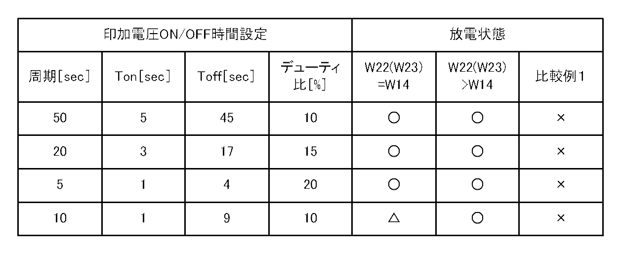
以上、本発明の各実施の形態について説明したが、本発明は前述の各実施の形態の構成に限定されるものではない。例えば、1つの電極子部組を構成する電極子部の数がN個(Nは3以上の整数)であってもよい。この場合、電極は、N(Nは4以上の整数)の倍数個の電極子部を有する。
Claims (15)
- 誘電体基板と、
前記誘電体基板の一方主面に設けられた第1櫛形電極と第2櫛形電極とを備え、
前記第1櫛形電極は、第1端子電極部と、前記第1端子電極部と交差する複数の第1電極子部組とを有し、
前記第2櫛形電極は、第2端子電極部と、前記第2端子電極部と交差する複数の第2電極子部組とを有し、
前記第1電極子部組と前記第2電極子部組とは一方向に交互に並ぶように配置されており、
前記第1電極子部組及び前記第2電極子部組は、それぞれ、
複数の電極子部と、
前記複数の電極子部同士を連結する少なくとも1つの第1連結部と、を有する、
オゾン生成用素子。 - 前記第1連結部は、同一の第1電極子部組における複数の電極子部の前記第1端子電極部とは反対方向の端部同士、同一の第2電極子部組における複数の電極子部の前記第2端子電極部とは反対方向の端部同士を連結している、
請求項1に記載のオゾン生成用素子。 - 前記第1櫛形電極の電極子部の前記第1端子電極部とは反対方向の端部は、前記第2端子電極部から離間して配置され、
前記第2櫛形電極の電極子部の前記第2端子電極部とは反対方向の端部は、前記第1端子電極部から離間して配置され、
前記第1電極子部組と隣り合う前記第2電極子部組との間の第1距離は、前記第1櫛形電極の電極子部の前記第1端子電極部とは反対方向の端部と前記第2端子電極部との間の第2距離以下である、
請求項2に記載のオゾン生成用素子。 - 前記第1端子電極部は、前記複数の第1電極子部組のうちの前記一方向における一端に位置する第1電極子部組を構成する少なくとも1つの電極子部と、前記一方向における他端に位置する第1電極子部組を構成する少なくとも1つの電極子部と、に接続され、
前記第2端子電極部は、前記複数の第2電極子部組のうちの前記一方向における一端に位置する第2電極子部組を構成する少なくとも1つの電極子部と、前記一方向における他端に位置する第2電極子部組を構成する少なくとも1つの電極子部と、に接続され、
前記第1電極子部組は、前記複数の第1電極子部組のうちの前記一方向における両端に位置する2つの第1電極子部組を除く他の第1電極子部組を構成する少なくとも1つの電極子部と、隣り合う他の第1電極子部組を構成する少なくとも1つの電極子部と、を連結する第2連結部を更に有し、
前記第2電極子部組は、前記複数の第2電極子部組のうちの前記一方向における両端に位置する2つの第2電極子部組を除く他の第2電極子部組を構成する少なくとも1つの電極子部と、隣り合う他の第2電極子部組を構成する少なくとも1つの電極子部と、を連結する第2連結部を更に有する、
請求項1に記載のオゾン生成用素子。 - 互いに隣り合う前記第1電極子部組と前記第2電極子部組との間の第3距離は、前記第1電極子部組の前記第2連結部と前記第1端子電極部との間の第4距離以下である、
請求項4に記載のオゾン生成用素子。 - 前記第1連結部は、同一の第1電極子部組における複数の電極子部の前記第1端子電極部とは反対方向の端部同士、同一の第2電極子部組における複数の電極子部の前記第2端子電極部とは反対方向の端部同士を連結し、
前記第3距離は、前記第1電極子部組の前記第2連結部と前記第2電極子部組の前記第1連結部との間の第5距離以下である、
請求項5に記載のオゾン生成用素子。 - 前記第1端子電極部は、
前記複数の第1電極子部組のうちの前記一方向における一端に位置する第1電極子部組を構成する少なくとも1つの電極子部に接続される第1サブ端子電極部と、
前記複数の第1電極子部組のうちの前記一方向における他端に位置する第1電極子部組を構成する少なくとも1つの電極子部に接続される第2サブ端子電極部と、を有し、
前記第2端子電極部は、
前記複数の第2電極子部組のうちの前記一方向における一端に位置する第2電極子部組を構成する少なくとも1つの電極子部に接続される第3サブ端子電極部と、
前記複数の第2電極子部組のうちの前記一方向における他端に位置する第2電極子部組を構成する少なくとも1つの電極子部に接続される第4サブ端子電極部と、を有する、
請求項4から6のいずれか1項に記載のオゾン生成用素子。 - 前記電極子部の線幅は、100μm未満である、
請求項1から7のいずれか1項に記載のオゾン生成用素子。 - 前記第1距離は、100μm未満であり、
前記第2距離は、200μm以上である、
請求項3に記載のオゾン生成用素子。 - 前記第3距離は、100μm未満であり、
前記第4距離は、200μm以上である、
請求項5に記載のオゾン生成用素子。 - 前記誘電体基板の前記一方主面を覆う誘電体層を更に備える、
請求項1から10のいずれか1項に記載のオゾン生成用素子。 - 前記第1電極子部組を構成する複数の電極子部は、前記第1端子電極部に連なり、
前記第2電極子部組を構成する複数の電極子部は、前記第2端子電極部に連なっている、
請求項1から11のいずれか1項に記載のオゾン生成用素子。 - 前記誘電体基板は、互いに積層された複数の誘電体層を有し、
前記複数の誘電体層それぞれに厚さ方向に貫通する形で設けられた充填ビアと、
前記複数の誘電体層の積層方向において隣り合う2つの誘電体層の間に介在し前記誘電体層の厚さ方向に直交する方向に延出するとともに、前記2つの誘電体層それぞれに設けられた充填ビアに電気的に接続されるビア接続部と、を有し、
前記複数の誘電体層それぞれに設けられた充填ビアのいずれか1つは、他の充填ビアのうちの少なくとも1つに対して、前記誘電体層の厚さ方向に直交する方向にずれている、
請求項1から12のいずれか1項に記載のオゾン生成用素子。 - 前記第1端子電極部は、前記誘電体基板の一方主面に設けられた第1接続電極部を介して、前記複数の誘電体層のうち最も前記一方主面側に位置する誘電体層に設けられた第1充填ビアに電気的に接続され、
前記第2端子電極部は、前記誘電体基板の一方主面に設けられた第2接続電極部を介して、前記複数の誘電体層のうち最も前記一方主面側に位置する誘電体層に設けられた第2充填ビアに電気的に接続され、
前記第1接続電極部における、前記誘電体基板の厚さ方向において前記第1充填ビアと重なる領域を覆う第1緩衝部と、
前記第2接続電極部における、前記誘電体基板の厚さ方向において前記第2充填ビアと重なる領域を覆う第2緩衝部と、を更に備える、
請求項13に記載のオゾン生成用素子。 - 請求項1から14のいずれか1項に記載のオゾン生成用素子と、
前記第1櫛形電極と前記第2櫛形電極の間に交流電圧を印加する交流電源と、を備える、
オゾン生成装置。
Priority Applications (3)
| Application Number | Priority Date | Filing Date | Title |
|---|---|---|---|
| JP2018504023A JP6627963B2 (ja) | 2016-03-09 | 2017-01-12 | オゾン生成用素子およびオゾン生成装置 |
| CN201780015622.3A CN108778989B (zh) | 2016-03-09 | 2017-01-12 | 臭氧生成用元件以及臭氧生成装置 |
| DE112017000681.3T DE112017000681T5 (de) | 2016-03-09 | 2017-01-12 | Ozongenerierungs-Bauelement und Ozongenerierungsvorrichtung |
Applications Claiming Priority (4)
| Application Number | Priority Date | Filing Date | Title |
|---|---|---|---|
| JP2016-045477 | 2016-03-09 | ||
| JP2016045477 | 2016-03-09 | ||
| JP2016-213081 | 2016-10-31 | ||
| JP2016213081 | 2016-10-31 |
Publications (1)
| Publication Number | Publication Date |
|---|---|
| WO2017154338A1 true WO2017154338A1 (ja) | 2017-09-14 |
Family
ID=59790201
Family Applications (1)
| Application Number | Title | Priority Date | Filing Date |
|---|---|---|---|
| PCT/JP2017/000754 Ceased WO2017154338A1 (ja) | 2016-03-09 | 2017-01-12 | オゾン生成用素子およびオゾン生成装置 |
Country Status (4)
| Country | Link |
|---|---|
| JP (1) | JP6627963B2 (ja) |
| CN (1) | CN108778989B (ja) |
| DE (1) | DE112017000681T5 (ja) |
| WO (1) | WO2017154338A1 (ja) |
Families Citing this family (1)
| Publication number | Priority date | Publication date | Assignee | Title |
|---|---|---|---|---|
| CN115594152B (zh) * | 2021-07-09 | 2024-07-09 | 财团法人工业技术研究院 | 臭氧产生装置以及臭氧产生方法 |
Citations (6)
| Publication number | Priority date | Publication date | Assignee | Title |
|---|---|---|---|---|
| JPH01246104A (ja) * | 1988-03-25 | 1989-10-02 | Kyocera Corp | オゾン発生用放電体 |
| JPH10287407A (ja) * | 1997-04-07 | 1998-10-27 | Yaskawa Electric Corp | オゾン発生装置 |
| JP2001080909A (ja) * | 1999-09-09 | 2001-03-27 | Yaskawa Electric Corp | オゾン発生器 |
| JP2002154810A (ja) * | 2000-11-15 | 2002-05-28 | Sekisui Chem Co Ltd | オゾン生成方法及びその装置 |
| JP2005213130A (ja) * | 2004-02-02 | 2005-08-11 | Toshiba Corp | オゾン発生ユニット及びオゾン発生装置 |
| JP2014186900A (ja) * | 2013-03-25 | 2014-10-02 | Murata Mfg Co Ltd | 放電素子およびその製造方法 |
Family Cites Families (9)
| Publication number | Priority date | Publication date | Assignee | Title |
|---|---|---|---|---|
| JP3844890B2 (ja) * | 1998-08-25 | 2006-11-15 | 東芝Itコントロールシステム株式会社 | オゾン発生装置 |
| CN2546431Y (zh) * | 2002-05-19 | 2003-04-23 | 刘德君 | 高浓臭氧发生器 |
| CN2609911Y (zh) * | 2003-04-16 | 2004-04-07 | 薛荃 | 臭氧发生器 |
| CA2547373A1 (en) * | 2006-05-18 | 2007-11-18 | Ozomax Inc. | Miniature ozone generator with internal or external power supply for purifiying water |
| JP4709712B2 (ja) * | 2006-08-24 | 2011-06-22 | 株式会社東芝 | オゾン発生装置 |
| KR20150022316A (ko) * | 2013-08-22 | 2015-03-04 | 주식회사 에코원테크놀로지 | 전기적 연결 방법이 개선된 오존발생장치 |
| JP2016045477A (ja) | 2014-08-27 | 2016-04-04 | リコーイメージング株式会社 | カメラ |
| CN204550051U (zh) * | 2015-02-12 | 2015-08-12 | 江苏海事职业技术学院 | 一种臭氧发生器 |
| JP6394981B2 (ja) | 2015-05-11 | 2018-09-26 | 住友電装株式会社 | レバー式コネクタ |
-
2017
- 2017-01-12 JP JP2018504023A patent/JP6627963B2/ja active Active
- 2017-01-12 DE DE112017000681.3T patent/DE112017000681T5/de active Pending
- 2017-01-12 WO PCT/JP2017/000754 patent/WO2017154338A1/ja not_active Ceased
- 2017-01-12 CN CN201780015622.3A patent/CN108778989B/zh active Active
Patent Citations (6)
| Publication number | Priority date | Publication date | Assignee | Title |
|---|---|---|---|---|
| JPH01246104A (ja) * | 1988-03-25 | 1989-10-02 | Kyocera Corp | オゾン発生用放電体 |
| JPH10287407A (ja) * | 1997-04-07 | 1998-10-27 | Yaskawa Electric Corp | オゾン発生装置 |
| JP2001080909A (ja) * | 1999-09-09 | 2001-03-27 | Yaskawa Electric Corp | オゾン発生器 |
| JP2002154810A (ja) * | 2000-11-15 | 2002-05-28 | Sekisui Chem Co Ltd | オゾン生成方法及びその装置 |
| JP2005213130A (ja) * | 2004-02-02 | 2005-08-11 | Toshiba Corp | オゾン発生ユニット及びオゾン発生装置 |
| JP2014186900A (ja) * | 2013-03-25 | 2014-10-02 | Murata Mfg Co Ltd | 放電素子およびその製造方法 |
Also Published As
| Publication number | Publication date |
|---|---|
| JPWO2017154338A1 (ja) | 2018-09-20 |
| CN108778989A (zh) | 2018-11-09 |
| CN108778989B (zh) | 2021-10-26 |
| DE112017000681T5 (de) | 2018-10-31 |
| JP6627963B2 (ja) | 2020-01-08 |
Similar Documents
| Publication | Publication Date | Title |
|---|---|---|
| CN107293401B (zh) | 多层陶瓷电容器及用于多层陶瓷电容器的安装板 | |
| US20170323727A1 (en) | Layered ceramic capacitor | |
| JP6919787B2 (ja) | 積層型電子部品の製造方法 | |
| CN101199062A (zh) | 用于冷却的压电驱动器 | |
| US9386678B2 (en) | Plasma generator and plasma generating device | |
| JP5481567B2 (ja) | イオン風発生体及びイオン風発生装置 | |
| US9036325B2 (en) | Ion wind generator and ion wind generating device | |
| JP6627963B2 (ja) | オゾン生成用素子およびオゾン生成装置 | |
| JP2005235976A (ja) | 積層セラミックコンデンサおよびその製造方法 | |
| JP6610771B2 (ja) | オゾン生成用素子およびオゾン生成装置 | |
| JP2012166976A (ja) | 誘電体磁器組成物およびセラミック電子部品 | |
| JP5668134B2 (ja) | イオン風発生体及びイオン風発生装置 | |
| JP6033651B2 (ja) | プラズマ発生体及びプラズマ発生装置 | |
| US10978635B2 (en) | Piezoelectric element, piezoelectric actuator and piezoelectric transformer | |
| JP2018026480A (ja) | セラミック配線基板及びセラミック配線基板の製造方法 | |
| JP6354865B2 (ja) | オゾン生成装置 | |
| CN107635914B (zh) | 臭氧生成装置 | |
| JP6350680B2 (ja) | オゾン生成装置 | |
| JP2008124276A (ja) | 電子部品の製造方法 | |
| JP2009032778A (ja) | 圧電トランスの製造方法 | |
| JP2015032411A (ja) | 静電気保護部品及び静電気保護部品の製造方法 | |
| JP2008198793A (ja) | 電子部品の製造方法 | |
| JP2016197489A (ja) | イオン発生素子 |
Legal Events
| Date | Code | Title | Description |
|---|---|---|---|
| ENP | Entry into the national phase |
Ref document number: 2018504023 Country of ref document: JP Kind code of ref document: A |
|
| WWE | Wipo information: entry into national phase |
Ref document number: 112017000681 Country of ref document: DE |
|
| 121 | Ep: the epo has been informed by wipo that ep was designated in this application |
Ref document number: 17762685 Country of ref document: EP Kind code of ref document: A1 |
|
| 122 | Ep: pct application non-entry in european phase |
Ref document number: 17762685 Country of ref document: EP Kind code of ref document: A1 |