WO2017145380A1 - 直流高圧電源装置 - Google Patents
直流高圧電源装置 Download PDFInfo
- Publication number
- WO2017145380A1 WO2017145380A1 PCT/JP2016/055881 JP2016055881W WO2017145380A1 WO 2017145380 A1 WO2017145380 A1 WO 2017145380A1 JP 2016055881 W JP2016055881 W JP 2016055881W WO 2017145380 A1 WO2017145380 A1 WO 2017145380A1
- Authority
- WO
- WIPO (PCT)
- Prior art keywords
- voltage
- negative
- positive
- output
- switch
- Prior art date
- Legal status (The legal status is an assumption and is not a legal conclusion. Google has not performed a legal analysis and makes no representation as to the accuracy of the status listed.)
- Ceased
Links
Images



Classifications
-
- H—ELECTRICITY
- H01—ELECTRIC ELEMENTS
- H01J—ELECTRIC DISCHARGE TUBES OR DISCHARGE LAMPS
- H01J49/00—Particle spectrometers or separator tubes
- H01J49/02—Details
- H01J49/06—Electron- or ion-optical arrangements
-
- H—ELECTRICITY
- H01—ELECTRIC ELEMENTS
- H01J—ELECTRIC DISCHARGE TUBES OR DISCHARGE LAMPS
- H01J49/00—Particle spectrometers or separator tubes
- H01J49/02—Details
- H01J49/10—Ion sources; Ion guns
-
- H—ELECTRICITY
- H02—GENERATION; CONVERSION OR DISTRIBUTION OF ELECTRIC POWER
- H02M—APPARATUS FOR CONVERSION BETWEEN AC AND AC, BETWEEN AC AND DC, OR BETWEEN DC AND DC, AND FOR USE WITH MAINS OR SIMILAR POWER SUPPLY SYSTEMS; CONVERSION OF DC OR AC INPUT POWER INTO SURGE OUTPUT POWER; CONTROL OR REGULATION THEREOF
- H02M7/00—Conversion of AC power input into DC power output; Conversion of DC power input into AC power output
- H02M7/02—Conversion of AC power input into DC power output without possibility of reversal
- H02M7/04—Conversion of AC power input into DC power output without possibility of reversal by static converters
- H02M7/06—Conversion of AC power input into DC power output without possibility of reversal by static converters using discharge tubes without control electrode or semiconductor devices without control electrode
- H02M7/10—Conversion of AC power input into DC power output without possibility of reversal by static converters using discharge tubes without control electrode or semiconductor devices without control electrode arranged for operation in series, e.g. for multiplication of voltage
Definitions
- the present invention relates to a DC high-voltage power supply device, and more particularly to a DC high-voltage power supply device capable of switching between positive and negative polarities of a DC high-voltage output.
- the mass spectrometer In the mass spectrometer, various compounds in the sample are ionized, and the generated ions are separated and detected according to the mass-to-charge ratio, and the compound is identified or quantified based on the detection signal. Some compounds are easily positively ionized and others are easily negatively ionized. Therefore, in a chromatographic mass spectrometer combining a chromatograph such as a gas chromatograph (GC) or a liquid chromatograph (LC) and a mass spectrometer, in order to detect various compounds without leakage, it is necessary to measure positive ions. It is desirable to perform this together with the measurement of negative ions. Therefore, as disclosed in Patent Document 1, Non-Patent Document 1, etc., the conventional chromatograph mass spectrometer has a function of repeatedly measuring while alternately switching between the positive ion measurement mode and the negative ion measurement mode. ing.
- a chromatograph such as a gas chromatograph (GC) or a liquid chromatograph (LC)
- the positive ion measurement mode and the negative ion measurement mode for example, it is necessary to switch the polarity of the voltage applied to each part such as an ion source, a mass separator, and an ion detector of the mass spectrometer.
- a pulsed voltage applied to an accelerating electrode when ions are ejected into flight space a DC voltage applied to a reflective electrode of the reflectron, a microchannel plate of an ion detector or a multistage
- FIG. 4 is an equivalent circuit of an example of a conventional DC high voltage power supply device.
- This power supply apparatus includes a positive voltage generator 1A that generates a positive high voltage + HV, a negative voltage generator 1B that generates a negative high voltage -HV, a high voltage switch 3A on the positive side, and a negative voltage generator 3B.
- the positive voltage generator 1A includes an excitation circuit 1A1 that outputs an alternating high voltage, a rectifier circuit 1A2 that converts the alternating high voltage into a direct high voltage, a filter circuit 1A3 that removes a ripple component included in the direct high voltage, including.
- the negative voltage generator 1B includes an excitation circuit 1B1 that outputs an alternating high voltage, a rectifier circuit 1B2 that converts the alternating high voltage into a direct high voltage, and a filter circuit 1B3 that removes a ripple component included in the direct high voltage. And including.
- the discharge resistors 9A and 9B are for discharging the charges accumulated in the capacitors 21A and 21B included in the rectifier circuits 1A2 and 1B2, the capacitors 31A and 31B included in the filter circuits 1A3 and 1B3, and the output capacitor 4. is there.
- the excitation circuits 1A1 and 1B1 are AC-DC converters that convert commercial AC power into DC power in order to generate AC high voltage of several kV or more, and switching that switches DC current by the AC-DC converter.
- the element includes a transformer including a primary winding to which the switched current is supplied.
- FIG. 6 is an operation explanatory diagram of the DC high-voltage power supply device
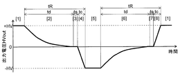
- FIG. 5 is a waveform diagram of the voltage HVout output from the voltage output terminal 6.
- Phase [1] is a state in which positive high voltage + HV is steadily output
- Phase [5] is a state in which negative high voltage -HV is steadily output.
- the state of each part is changed from Phase [1] positive voltage steady output state to Phase [2] ⁇ [3] ⁇ [4] It changes in order until the negative voltage steady output state of [5].
- the positive side excitation circuit 1A1 is in an on (operating) state, and the positive side high voltage switch 3A is also in an on (closed) state.
- the negative side excitation circuit 1B is in an off (non-operating) state, and the negative side high voltage switch 3B is also in an off (open) state.
- the DC positive voltage + HV generated by the positive voltage generator 1A is applied to the load 100 and the output capacitor 4 via the high voltage switch 3A and the protective resistor 5A.
- the operation of the positive side excitation circuit 1A1 is stopped (turned off) while the positive side high voltage switch 3A is maintained in the on (closed) state.
- the electric charges accumulated in the capacitor 31A and the output capacitor 4 in the positive filter circuit 1A3 until immediately before are discharged through the discharging resistor 9A as shown by the bold arrow and the thick dotted arrow in FIG. 6B. .
- the output voltage HVout decreases exponentially from + HV as shown in FIG.
- the resistance value of the protective resistor 5A is sufficiently smaller than the resistance value of the discharging resistor 9A and can be ignored.
- the time constant of discharge is the resistance value of the discharge resistor 9A and the capacitance value of the capacitor 31A in the filter circuit 1A3 (strictly speaking, the parallel combined capacitance value of the capacitor 31A and the capacitor 21A in the positive rectifier circuit 1A2). ) And the parallel composite capacitance value of the output capacitor 4 capacitance value.
- the negative side excitation circuit 1B1 is changed from the off (non-operating) state to the on (operating) state.
- a current flows as indicated by a thick arrow in FIG.
- the output capacitor 4 is charged to a negative polarity, and the output voltage HVout rises to the negative polarity side as shown in FIG.
- the phase shifts from Phase [4] to [5].
- the negative side excitation circuit 1B1 is maintained in the on (operating) state, and the negative side high voltage switch 3B is maintained in the on (closed) state.
- the DC negative voltage -HV generated by the negative voltage generating circuit 1B is applied to the load 100 and the output capacitor 4 via the high voltage switch 3B and the protective resistor 5B.
- the polarity switching from the positive polarity to the negative polarity is completed.
- Phase [6] the operation of the negative side excitation circuit 1B1 is stopped (turned off) while the negative side high voltage switch 3B is maintained in the on (closed) state.
- the charges accumulated in the capacitor 31B and the output capacitor 4 in the negative filter circuit 1B3 until immediately before are discharged through the discharging resistor 9B, as shown by the thick arrow and the thick dotted arrow in FIG. 6 (f). .
- the output voltage HVout decreases exponentially from ⁇ HV as shown in FIG.
- the resistance value of the protective resistor 5B is sufficiently smaller than the resistance value of the discharging resistor 9B and can be ignored.
- the time constant of discharge is the resistance value of the discharge resistor 9B and the capacitance value of the capacitor 31B in the filter circuit 1B3 (strictly speaking, the parallel combined capacitance value of this capacitor 31B and the capacitor 21B in the positive side rectifier circuit 1B2). ) And the parallel composite capacitance value of the output capacitor 4 capacitance value.
- Phase [8] the positive side excitation circuit 1A1 is switched from the off (non-operating) state to the on (operating) state. As a result, a current flows as indicated by a thick arrow in FIG.
- the output capacitor 4 is charged to the positive polarity, and the output voltage HVout rises to the positive polarity side as shown in FIG.
- the phase shifts from Phase [8] to [1].
- the time required to switch the polarity of the output voltage HVout from positive to negative or vice versa is the capacitors 21A and 21B in the rectifier circuits 1A2 and 1B2, the filter circuit 1A3, A discharge time td for discharging the charges accumulated in the capacitors 31A and 31B and the output capacitor 4 in 1B3 through the discharge resistors 9A and 9B to reduce the output voltage HVout to almost zero, and the high voltage switch 3A,
- This is the total time of the switching time ts required for switching 3B and the charging time tc for operating the excitation circuits 1A1 and 1B1 from the non-operating state to raise the output voltage HVout to the desired voltage value ⁇ HV.
- the discharge time td includes the resistance values of the discharge resistors 9A and 9B, the positive and negative voltage generators 1A and 1B side capacitors (the capacitors 21A and 21B in the rectifier circuits 1A2 and 1B2, and the capacitors 31A and 31B in the filter circuits 1A3 and 1B3). ) And the capacitance value of the output capacitor 4 are proportional to the time constant determined by the parallel composite capacitance value.
- the charging time tc is inversely proportional to the current capacity that can be supplied by the positive and negative voltage generators 1A and 1B.
- the present invention has been made to solve the above-mentioned problems, and the object of the present invention is to reduce the output voltage while minimizing the increase in the cost of the device, the increase in size and weight, and the temperature rise in the device as much as possible. It is to provide a DC high-voltage power supply device capable of speeding up the switching of the polarity.
- the present invention provides a DC high-voltage power supply apparatus that selectively outputs positive and negative DC high voltages.
- a positive-side AC voltage generating unit that generates an AC voltage, and a rectifying / smoothing unit that rectifies and smoothes the AC voltage, and outputs a positive DC high voltage
- a negative voltage generator that outputs a negative DC high voltage, including a negative AC voltage generator that generates an AC voltage, and a rectifying / smoothing unit that rectifies and smoothes the AC voltage
- a first output circuit in which a positive switch and a protective resistor are connected in series, connected between a voltage output terminal of the positive voltage generator and a positive / negative switching voltage output terminal that is common to positive and negative
- control unit for controlling the operations of the positive-side AC voltage generation unit and the negative-side AC voltage generation unit, and the open / close operation of the positive-side switch and the negative-side switch so that both the negative-side switch and the negative-side switch are closed.
- the positive switch when a positive high voltage is steadily output to a load connected to the positive / negative switching voltage output terminal, the positive switch is closed and the negative switch is opened.
- the positive-side AC voltage generator is in an operating state
- the negative-side AC voltage generator is in a non-operational state, that is, in a stopped state.
- the positive side switch is opened, the negative side switch is closed, the negative side AC voltage generator is in the operating state, and the positive side AC voltage generator. Is in a non-operational state, that is, a stopped state.
- the output capacitor and the capacitor included in the rectifying / smoothing unit are charged by the power supplied from the positive voltage generating unit or the negative voltage generating unit to the load.
- the control unit stops the operation of the positive side AC voltage generation unit and closes the negative side switch. To do. As a result, the operation of the AC voltage generator is stopped on both the positive electrode side and the negative electrode side, while the switch is closed on both the positive electrode side and the negative electrode side. As a result, the positive charge accumulated in the output capacitor is discharged through the second output circuit and the negative diode. On the other hand, the electric charge accumulated in the capacitor included in the rectifying / smoothing unit of the positive voltage generating unit is discharged through the first output circuit, the second output circuit, and the diode on the negative electrode side.
- a loop including the second output circuit that is not formed because the negative switch is not closed is formed, and discharge is achieved through the loop.
- the loop includes a protective resistor.
- the time constant is small, so that the discharge is performed rapidly and the output voltage becomes zero in a short time.
- the loop since the loop includes a diode connected in the forward direction in the direction in which the discharge current flows, it is possible to prevent the discharge current from flowing through the rectification / smoothing unit of the negative voltage generation unit connected in parallel with the diode. Can do.
- the control unit opens the positive side switch and starts the operation of the negative side AC voltage generation unit, thereby generating the negative high voltage generated by the negative voltage generation unit. Can be output from the positive / negative switching voltage output terminal.
- the time required for switching the polarity of the output voltage can be shortened as compared with the conventional device.
- the DC high-voltage power supply device according to the present invention is used as a power source for various electrodes in a mass spectrometer of a chromatograph mass spectrometer, for example, the positive ion measurement mode and the negative ion measurement mode can be quickly switched. It is possible to shorten the measurement impossible period that accompanies the switching of the measurement mode and to reduce component detection omissions. Also, a better chromatogram can be created by shortening the cycle of switching between the positive ion measurement mode and the negative ion measurement mode.
- the equivalent circuit schematic of the DC high voltage power supply device by one Example of this invention The wave form diagram of the output voltage at the time of positive / negative polarity switching of the DC high voltage power supply device of a present Example. Operation
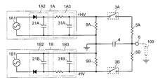
- FIG. 1 is an equivalent circuit diagram of a DC high-voltage power supply device according to the present embodiment
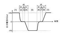
- FIG. 2 is a waveform diagram of an output voltage when switching the positive / negative polarity of the DC high-voltage power supply device according to the present embodiment
- FIG. FIG. 1 is an equivalent circuit diagram of a DC high-voltage power supply device according to the present embodiment
- FIG. 2 is a waveform diagram of an output voltage when switching the positive / negative polarity of the DC high-voltage power supply device according to the present embodiment
- symbol is attached
- the configurations of 5A, 5B, output capacitor 4 and the like are the same as those of the conventional DC high voltage power supply device.
- One of the differences between the DC high-voltage power supply device of the present embodiment and the conventional device is that instead of the discharge resistors 9A and 9B connected to the output terminals of the positive voltage generator 1A and the negative voltage generator 1B, This is that diodes 2A and 2B are provided.
- Both the discharge diodes 2A and 2B are connected in such a direction as to be in a reverse bias state by the voltages when the voltages are output to the output terminals of the positive voltage generator 1A and the negative voltage generator 1B, respectively. Further, the high voltage switches 3A and 3B are turned on / off by the drive unit 8, and the drive unit 8 and the excitation circuits 1A1 and 1B1 are operated by a control signal supplied from the control unit 7. The control sequence at the time of switching the positive / negative polarity of the output voltage is different from that of the conventional apparatus.
- Phase [1] is a state in which positive high voltage + HV is steadily output
- Phase [5] is a state in which negative high voltage -HV is steadily output.
- the state of each part is changed from Phase [1] positive voltage steady output state to Phase [2] ⁇ [3] ⁇ [4] and then Phase [ It changes in order until the negative voltage steady output state of [5].
- the positive side excitation circuit 1A1 is in an on (operation) state, and the positive side high voltage switch 3A is in an on (closed) state.
- the negative side excitation circuit 1B is in an off (non-operating) state, and the negative side high voltage switch 3B is in an off (open) state.
- the DC positive voltage + HV generated by the positive voltage generating circuit 1A is applied to the load 100 and the output capacitor 4 via the high voltage switch 3A and the protective resistor 5A.
- Phase [2] under the control of the control unit 7, the operation of the positive side excitation circuit 1A1 is stopped (turned off) while the positive side high voltage switch 3A is kept on (closed). ) Further, the negative side high voltage switch 3B is switched from the off (open) state to the on (closed) state. That is, in Phase [2], the excitation circuits 1A1 and 1B1 are both inactive, while the high voltage switches 3A and 3B are both on. As a result, the charges accumulated in the capacitor 31A in the positive filter circuit 1A3 until just before that are, as shown by the bold arrows in FIG.
- the charge accumulated in the output capacitor 4 is a closed loop including the negative electrode side protective resistor 5B, the negative electrode side high voltage switch 3B, and the negative electrode side discharging diode 2B, as shown by a thick dotted arrow in FIG. And is consumed by the protective resistor 5B.
- both the high-voltage switches 3A and 3B are turned on.
- a loop including 5B, the negative-side high-voltage switch 3B, and the negative-side discharge diode 2B is formed, and discharge through this loop becomes possible.
- a large discharge current that has passed through the negative-side protection resistor 5B and the negative-side high-voltage switch 3B flows to the negative voltage generation unit 1B. Since the circuit element may be destroyed, it is necessary to take measures such as using an element that can withstand the circuit element.
- this power supply device it is possible to avoid the discharge current from flowing through the negative voltage generator 1B by the negative-side discharge diode 2B, and the above measures are not required in the voltage generators 1A and 1B.
- the discharge The time constant depends on the product of the resistance value of the negative protection resistor 5B and the capacitance value of the output capacitor 4.
- the resistance values of the protective resistors 5A and 55B are considerably smaller than the resistance values of the discharging resistors 9A and 9B in the conventional device. Therefore, the time constant of this discharge is smaller than that of the conventional device, and the output voltage HVout becomes zero in a short time as shown in FIG.
- Phase [3] after the output voltage HVout becomes almost zero, the positive side high voltage switch 3A is turned off (open) from the on (closed) state while the negative side high voltage switch 3B is kept in the off state. Switch. As a result, the same state as Phase [3] in the conventional apparatus shown in FIG.
- Phase [4] the negative side excitation circuit 1B1 is changed from the off (non-operating) state to the on (operating) state. As a result, a current flows as indicated by a thick arrow in FIG.
- the output capacitor 4 is charged to a negative polarity, and the output voltage HVout increases to the negative polarity side as shown in FIG.
- the phase shifts from Phase [4] to [5].
- the negative side excitation circuit 1B1 is maintained in the on (operating) state, and the negative side high voltage switch 3B is maintained in the on (closed) state.
- the DC negative voltage -HV generated by the negative voltage generating circuit 1B is applied to the load and the output capacitor 4 via the high voltage switch 3B and the protective resistor 5B.
- the polarity switching from the positive polarity to the negative polarity is completed.
- Phase [6] under the control of the control unit 7, the operation of the negative side excitation circuit 1B1 is stopped (turned off) while the negative side high voltage switch 3B is maintained in the on (closed) state. . Further, the positive side high voltage switch 3A is switched from the off (open) state to the on (closed) state. That is, in Phase [6], as in Phase [2], both excitation circuits 1A1 and 1B1 are inactive, while high voltage switches 3A and 3B are both on. As a result, the charge accumulated in the capacitor 31B in the negative filter circuit 1B3 until just before that is, as shown by the bold arrow in FIG. 3 (f), the negative discharge diode 2A, the positive high voltage switch 3A.
- the positive-side protection resistor 5A, the negative-side protection resistor 5B, and the negative-side high-voltage switch 3B are discharged in a closed loop and consumed by the protection resistors 5A and 5B (converted into heat).
- the charge accumulated in the output capacitor 4 includes the positive-side discharge diode 2A, the positive-side protection resistor 5A, and the positive-side high-voltage switch 3A, as shown by the thick dotted arrows in FIG. It is discharged in a closed loop and consumed by the protective resistor 5A.
- the discharge time constant is smaller than that of the conventional apparatus, as shown in FIG.
- the output voltage HVout becomes zero in a short time.
- Phase [7] after the output voltage HVout becomes almost zero, the negative-side high-voltage switch 3B is switched from the on (closed) state to the off (open) state. As a result, the same state as Phase [7] in the conventional apparatus shown in FIG.
- Phase [8] the positive side excitation circuit 1A1 is changed from the off (non-operating) state to the on (operating) state. Thereby, like FIG.6 (h), an electric current flows as shown by the thick line arrow in FIG.3 (h).
- the output capacitor 4 is charged to the positive polarity, and the output voltage HVout rises to the positive polarity side as shown in FIG.
- the phase shifts from Phase [8] to [1].
- the polarity reversal time tR is the total time of the discharge time td, the switching time ts, and the charge time tc.
- the switching time ts and the charging time tc are the same as those of the conventional device.
- the discharge time td is shorter than that of the conventional apparatus.
- the polarity reversal time tR is shortened compared to the conventional device, and switching between positive and negative is possible.
- the polarity reversal time tR between the DC high-voltage power supply device of the present embodiment and the conventional device is specifically compared.
- conditions were defined as follows.
- the output voltages ⁇ HV of the positive and negative voltage generators 1A and 1B are ⁇ 10 kV.
- the positive and negative voltage generators 1A and 1B have a power supply capacity of 10 W and an output current of 1 mA.
- the capacity of the output capacitor 4 combined with the capacity of the load 100 is 10 nF, and the capacities of the capacitors 21A, 31A, 21B, 31B included in the voltage generators 1A, 1B are all compared to the capacity of the output capacitor 4. Small enough to be negligible.
- the resistance value of the load 100 is sufficiently larger than the output impedance of the power supply device, and the current flowing through the load 100 can be ignored.
- the maximum switching power of the high voltage switches 3A and 3B is 100 W, and the switching time ts is 1 msec.
- the steady power consumption of the discharge resistors 9A and 9B in the conventional apparatus is 1 W or less.
- the DC high-voltage power supply device does not require a discharge resistor, power loss during steady output (1 W under the above conditions) does not occur, and the temperature inside the power supply device increases by that much. There is also an advantage that it can be suppressed. As a result, the anxiety of the output voltage due to the temperature rise is eliminated, and the stability of the output voltage is improved.
- the high voltage switches 3A and 3B may be configured using other switching elements such as a bipolar transistor, an insulated gate bipolar transistor (IGBT), and a mechanical relay in addition to the MOSFET.
- IGBT insulated gate bipolar transistor
- the breakdown voltage per element can be suppressed by adopting a configuration in which a plurality of diodes and corresponding elements are connected in series. Of course it is also possible.
- the excitation circuits 1A1 and 1B1 may have any configuration as long as an AC high voltage can be output.
- an AC-DC converter that converts commercial AC power into DC power
- the AC-DC converter preferably includes a switching element such as a MOSFET for switching a direct current, a transformer including a primary winding to which the switched current is supplied, and the like.
Landscapes
- Engineering & Computer Science (AREA)
- Chemical & Material Sciences (AREA)
- Analytical Chemistry (AREA)
- Power Engineering (AREA)
- Physics & Mathematics (AREA)
- Plasma & Fusion (AREA)
- Electron Tubes For Measurement (AREA)
- Rectifiers (AREA)
- Dc-Dc Converters (AREA)
Abstract
正イオン測定と負イオン測定との切替えを高速化するために出力高電圧の正負を高速に切り替え可能な直流高圧電源装置を提供する。正極側の励振回路(1A1)をオン、高電圧スイッチ(3A)をオンすることで正極性の高電圧を電圧出力端(6)から出力している状態から電圧の極性を切り替える際には、制御部(7)は励振回路(1A1)をオフするとともに負極側の高電圧スイッチ(3B)をオンする。高電圧スイッチ(3A、3B)が共にオンするため、その直前に出力コンデンサ(4)に蓄積していた電荷やフィルタ回路(1A3)のコンデンサ(31A)に蓄積していた電荷は保護抵抗5B、高電圧スイッチ(3B)、ダイオード(2B)を含む経路で放電される。保護抵抗(5A、5B)の抵抗値は小さいので放電の時定数は小さく、放電用抵抗を用いた従来装置に比べて出力電圧を迅速に零にすることができ、正負極性の切替えを高速化することができる。
Description
本発明は直流高圧電源装置に関し、さらに詳しくは、直流高電圧出力の正負の極性切替えが可能である直流高圧電源装置に関する。
質量分析装置では、試料中の各種化合物をイオン化し、生成されたイオンを質量電荷比に応じて分離して検出し、その検出信号に基づいて化合物を同定したり該化合物を定量したりする。化合物には正イオン化され易いものと負イオン化され易いものとがある。そのため、ガスクロマトグラフ(GC)や液体クロマトグラフ(LC)等のクロマトグラフと質量分析装置とを組み合わせたクロマトグラフ質量分析装置において、様々な化合物をできるだけ漏れなく検出するには、正イオンの測定と負イオンの測定とを併せて行うことが望ましい。そこで、特許文献1、非特許文献1等に開示されているように、従来のクロマトグラフ質量分析装置は、正イオン測定モードと負イオン測定モードとを交互に切り換えながら繰り返し測定を行う機能を備えている。
正イオン測定モードと負イオン測定モードとでは、例えば質量分析装置のイオン源、質量分離器、イオン検出器などの各部に印加する電圧の極性を切り替える必要がある。例えばリフレクトロン飛行時間型質量分析装置では、イオンを飛行空間に射出する際に加速電極に印加するパルス状の電圧、リフレクトロンの反射電極に印加する直流電圧、イオン検出器のマイクロチャンネルプレートや多段ダイノードなどに印加する直流電圧などの極性を、検出対象のイオンの極性に応じて切り替える必要がある。正イオン測定モードと負イオン測定モードとを高速に切り替えるには、上記のような各種印加電圧の極性の切替えを高速に行う必要があり、1系統の出力電圧の極性の切替えが高速に行える直流高圧電源装置が従来使用されている。
図4は従来の直流高圧電源装置の一例の等価回路である。この電源装置は、正極性の高電圧+HVを発生する正電圧発生部1Aと、負極性の高電圧-HVを発生する負電圧発生部1Bと、正極側の高電圧スイッチ3Aと、負極側の高電圧スイッチ3Bと、それら高電圧スイッチ3A、3Bに流れるサージ電流を制限する保護抵抗5A、5Bと、電圧出力端6に接続される負荷100の電位を安定化するために負荷100に並列に接続された出力コンデンサ4と、正電圧発生部1Aの出力端及び負電圧発生部1Bの出力端にそれぞれ並列に接続された放電用抵抗9A、9Bと、を含む。正電圧発生部1Aは、交流高電圧を出力する励振回路1A1と、該交流高電圧を直流高電圧に変換する整流回路1A2と、直流高電圧に含まれるリップル成分を除去するフィルタ回路1A3と、を含む。同様に負電圧発生部1Bは、交流高電圧を出力する励振回路1B1と、該交流高電圧を直流高電圧に変換する整流回路1B2と、直流高電圧に含まれるリップル成分を除去するフィルタ回路1B3と、を含む。放電用抵抗9A、9Bは、整流回路1A2、1B2に含まれるコンデンサ21A、21B、フィルタ回路1A3、1B3に含まれるコンデンサ31A、31B、及び出力コンデンサ4に蓄積された電荷を放電するためのものである。
なお、一般に、励振回路1A1、1B1は、数kV以上の交流高電圧を生成するために、商用交流電力を直流電力に変換するAC-DCコンバータ、該AC-DCコンバータによる直流電流をスイッチングするスイッチング素子、そのスイッチングされた電流が供給される1次巻線を含むトランスなどを含んで構成される。
図6はこの直流高圧電源装置の動作説明図、図5は電圧出力端6から出力される電圧HVoutの波形図である。図6において、Phase[1]は正極性の高電圧+HVを定常的に出力する状態、Phase[5]は負極性の高電圧-HVを定常的に出力する状態である。この出力電圧の極性を正極性から負極性に変化させる際には、各部の状態は、Phase[1]の正電圧定常出力状態から、Phase[2]→[3]→[4]を経てPhase[5]の負電圧定常出力状態まで順に変化する。一方、出力電圧の極性を負極性から正極性に変化させる際には、各部の状態は、Phase[5]の負電圧定常出力状態から、Phase[6]→[7]→[8]を経てPhase[1]の正電圧定常出力状態まで順に変化する。図5中の[1]~[8]の各期間は図6中のPhase[1]~Phase[8]に対応する。
以下、極性切替え時の動作を説明する。
図6(a)に示すように、Phase[1]では、正極側励振回路1A1はオン(動作)状態、正極側高電圧スイッチ3Aもオン(閉成)状態である。他方、負極側励振回路1Bはオフ(非動作)状態、負極側高電圧スイッチ3Bもオフ(開成)状態である。このとき、正電圧発生部1Aで生成された直流正電圧+HVが、高電圧スイッチ3A、保護抵抗5Aを介して負荷100及び出力コンデンサ4に印加される。図6(a)中に太線矢印で示すように、電流が流れ(ただし、負荷100に流れる電流の記載は省略している)、出力コンデンサ4及びフィルタ回路1A3中のコンデンサ31Aはそれぞれ図6(a)中に記載のように蓄電される。なお、整流回路1A2中のコンデンサ21Aも同様に蓄電されるが、通常、このコンデンサ21Aの容量はフィルタ回路1A3中のコンデンサ31Aの容量に比べて十分に小さいので、無視するものとする。これは以下の説明でも同様である。
図6(a)に示すように、Phase[1]では、正極側励振回路1A1はオン(動作)状態、正極側高電圧スイッチ3Aもオン(閉成)状態である。他方、負極側励振回路1Bはオフ(非動作)状態、負極側高電圧スイッチ3Bもオフ(開成)状態である。このとき、正電圧発生部1Aで生成された直流正電圧+HVが、高電圧スイッチ3A、保護抵抗5Aを介して負荷100及び出力コンデンサ4に印加される。図6(a)中に太線矢印で示すように、電流が流れ(ただし、負荷100に流れる電流の記載は省略している)、出力コンデンサ4及びフィルタ回路1A3中のコンデンサ31Aはそれぞれ図6(a)中に記載のように蓄電される。なお、整流回路1A2中のコンデンサ21Aも同様に蓄電されるが、通常、このコンデンサ21Aの容量はフィルタ回路1A3中のコンデンサ31Aの容量に比べて十分に小さいので、無視するものとする。これは以下の説明でも同様である。
次のPhase[2]では、正極側高電圧スイッチ3Aがオン(閉成)状態に維持されたまま、正極側励振回路1A1の動作が停止される(オフされる)。その直前まで正極側フィルタ回路1A3中のコンデンサ31A及び出力コンデンサ4に蓄積されていた電荷は、図6(b)中に太線矢印及び太点線矢印で示すように、放電用抵抗9Aを通して放電される。これにより、出力電圧HVoutは図5中に示すように+HVから指数関数的に低下する。保護抵抗5Aの抵抗値は放電用抵抗9Aの抵抗値に比べて十分に小さく無視できる。そのため、放電の時定数は、放電用抵抗9Aの抵抗値と、フィルタ回路1A3中のコンデンサ31Aの容量値(厳密にはこのコンデンサ31Aと正極側整流回路1A2中のコンデンサ21Aとの並列合成容量値)と出力コンデンサ4の容量値との並列合成容量値との積に依存する。
Phase[3]では、出力電圧HVoutがほぼゼロになったあと、正極側高電圧スイッチ3Aをオン(閉成)状態からオフ(開成)に切り替える一方、負極側高電圧スイッチ3Bをオフ(開成)状態からオン(閉成)に切り替える。
続くPhase[4]では、負極側励振回路1B1をオフ(非動作)状態からオン(動作)状態にする。これにより、図6(d)中に太線矢印で示すように電流が流れる。出力コンデンサ4は負極性に充電され、出力電圧HVoutは図5中に示すように負極性側に上昇してゆく。そして、出力電圧HVoutが所定の負電圧-HVに到達するとPhase[4]から[5]に移行する。
Phase[5]では、負極側励振回路1B1はオン(動作)状態、負極側高電圧スイッチ3Bはオン(閉成)状態に維持される。このとき、負電圧発生回路1Bで生成された直流負電圧-HVが、高電圧スイッチ3B、保護抵抗5Bを介して負荷100及び出力コンデンサ4に印加される。ここまでで、正極性から負極性への極性切替えが完了する。
Phase[6]では、負極側高電圧スイッチ3Bがオン(閉成)状態に維持されたまま、負極側励振回路1B1の動作が停止される(オフされる)。その直前まで負極側フィルタ回路1B3中のコンデンサ31B及び出力コンデンサ4に蓄積されていた電荷は、図6(f)中に太線矢印及び太点線矢印で示すように、放電用抵抗9Bを通して放電される。これにより、出力電圧HVoutは図5中に示すように-HVから指数関数的に低下する。保護抵抗5Bの抵抗値は放電用抵抗9Bの抵抗値に比べて十分に小さく無視できる。そのため、放電の時定数は、放電用抵抗9Bの抵抗値と、フィルタ回路1B3中のコンデンサ31Bの容量値(厳密にはこのコンデンサ31Bと正極側整流回路1B2中のコンデンサ21Bとの並列合成容量値)と出力コンデンサ4の容量値との並列合成容量値との積に依存する。
Phase[7]では、出力電圧HVoutがほぼゼロになったあと、負極側高電圧スイッチ3Bをオン(閉成)状態からオフ(開成)に切り替える一方、正極側高電圧スイッチ3Aをオフ(開成)状態からオン(閉成)に切り替える。
Phase[8]では、正極側励振回路1A1をオフ(非動作)状態からオン(動作)状態にする。これにより、図6(h)中に太線矢印で示すように電流が流れる。出力コンデンサ4は正極性に充電され、出力電圧HVoutは図5中に示すように正極性側に上昇してゆく。そして、出力電圧HVoutが所定の正電圧+HVに到達するとPhase[8]から[1]に移行する。
図5に示すように、出力電圧HVoutの極性を正から負へ又はその逆に切り替えるのに要する時間、即ち極性反転時間tRは、整流回路1A2、1B2中のコンデンサ21A、21B、フィルタ回路1A3、1B3中のコンデンサ31A、31B、及び出力コンデンサ4にそれぞれ蓄積された電荷を放電用抵抗9A、9Bを通して放出して出力電圧HVoutをほぼゼロまで低下させるための放電時間tdと、高電圧スイッチ3A、3Bの切替えに要する切替時間tsと、励振回路1A1、1B1を非動作状態から動作させて出力電圧HVoutを所望の電圧値±HVまで上昇させるための充電時間tcと、を合計した時間である。
放電時間tdは、放電用抵抗9A、9Bの抵抗値、正負の電圧発生部1A、1B側のコンデンサ(整流回路1A2、1B2中のコンデンサ21A、21B及びフィルタ回路1A3、1B3中のコンデンサ31A、31B)の容量値と出力コンデンサ4の容量値との並列合成容量値とで決まる時定数に比例する。充電時間tcは、正負の電圧発生部1A、1Bが供給可能である電流容量に反比例する。そのため、高電圧スイッチ3A、3Bの切替時間tsが一定であるとした場合、極性反転時間tRを短縮するには、上記時定数を小さくして放電時間tdを短縮するか、電圧発生部1A、1Bの電流容量を増大して充電時間tcを短縮するか、又はその両方を実施する必要がある。しかしながら、電圧発生部1A、1Bの電流容量を増加することは装置のコストアップや装置のサイズ・重量の増加に繋がるため制約がある。また、電圧発生部1A、1Bに含まれるコンデンサの容量や出力コンデンサ4の容量を小さくすると出力電圧のリップルやノイズが増加するおそれがあるため、やはり制約がある。したがって、一般的には、放電用抵抗9A、9Bの抵抗値を小さくすることで放電時間tdを短縮するという手法を採らざるをえない。
ところが、放電用抵抗9A、9Bの抵抗値を小さくすると、定常出力時に該抵抗9A、9Bに流れる電流が増加し、消費電力が増加して発熱量が多くなる。そのため、電源装置内部の温度上昇が大きくなり、出力電圧の安定度が悪化するという問題がある。これを回避するには、放電用抵抗9A、9B付近の放熱を促進する必要があり、装置の大形化等に繋がる。また、放電用抵抗9A、9Bで消費電力が増加するということは、それだけ電圧発生部1A、1Bの電流容量を増加させる必要が生じるため、程度の差はあれ、装置のコストアップにも繋がる。
「LCMS-IT-TOF 液体クロマトグラフ質量分析計 正負イオン高速切換測定」、[online]、株式会社島津製作所、[平成28年2月3日検索]、インターネット<URL: http://www.an.shimadzu.co.jp/lcms/it-tof3.htm>
本発明は上記課題を解決するために成されたものであり、その目的とするところは、装置のコストアップやサイズ・重量の増加、さらには装置内部の温度上昇などをできるだけ抑えながら、出力電圧の極性の切替えの高速化を図ることができる直流高圧電源装置を提供することである。
上記課題を解決するために成された本発明は、正負の両極性の直流高電圧を選択的に出力する直流高圧電源装置において、
a)交流電圧を発生する正極側交流電圧発生部、及び、該交流電圧を整流したあと平滑化する整流・平滑化部、を含み、正極性の直流高電圧を出力する正電圧発生部と、
b)交流電圧を発生する負極側交流電圧発生部、及び、該交流電圧を整流したあと平滑化する整流・平滑化部、を含み、負極性の直流高電圧を出力する負電圧発生部と、
c)前記正電圧発生部の電圧出力端及び前記負電圧発生部の電圧出力端にそれぞれ前記直流高電圧が出力される際に該電圧により逆方向バイアス状態となる向きに、前記電圧出力端にそれぞれ接続されたダイオードと、
d)前記正電圧発生部の電圧出力端と正負共通である正負切換電圧出力端との間に接続された、正極側スイッチと保護抵抗とが直列に接続された第1の出力回路と、
e)前記負電圧発生部の出力端と前記正負切換電圧出力端との間に接続された、負極側スイッチと保護抵抗とが直列に接続された第2の出力回路と、
f)前記正負切換電圧出力端に接続される負荷と並列に接続された出力コンデンサと、
g)前記正負切換電圧出力端からの出力電圧の正負の極性を切り替える際に、前記正極側交流電圧発生部及び前記負極側交流電圧発生部の動作を共に停止させた状態で、前記正極側スイッチ及び前記負極側スイッチを共に閉成するように、該正極側交流電圧発生部及び該負極側交流電圧発生部の動作、並びに、該正極側スイッチ及び該負極側スイッチの開閉動作を制御する制御部と、
を備えることを特徴としている。
a)交流電圧を発生する正極側交流電圧発生部、及び、該交流電圧を整流したあと平滑化する整流・平滑化部、を含み、正極性の直流高電圧を出力する正電圧発生部と、
b)交流電圧を発生する負極側交流電圧発生部、及び、該交流電圧を整流したあと平滑化する整流・平滑化部、を含み、負極性の直流高電圧を出力する負電圧発生部と、
c)前記正電圧発生部の電圧出力端及び前記負電圧発生部の電圧出力端にそれぞれ前記直流高電圧が出力される際に該電圧により逆方向バイアス状態となる向きに、前記電圧出力端にそれぞれ接続されたダイオードと、
d)前記正電圧発生部の電圧出力端と正負共通である正負切換電圧出力端との間に接続された、正極側スイッチと保護抵抗とが直列に接続された第1の出力回路と、
e)前記負電圧発生部の出力端と前記正負切換電圧出力端との間に接続された、負極側スイッチと保護抵抗とが直列に接続された第2の出力回路と、
f)前記正負切換電圧出力端に接続される負荷と並列に接続された出力コンデンサと、
g)前記正負切換電圧出力端からの出力電圧の正負の極性を切り替える際に、前記正極側交流電圧発生部及び前記負極側交流電圧発生部の動作を共に停止させた状態で、前記正極側スイッチ及び前記負極側スイッチを共に閉成するように、該正極側交流電圧発生部及び該負極側交流電圧発生部の動作、並びに、該正極側スイッチ及び該負極側スイッチの開閉動作を制御する制御部と、
を備えることを特徴としている。
本発明に係る直流高圧電源装置において、正負切換電圧出力端に接続された負荷に対し正極性の高電圧を定常的に出力する際には、正極側スイッチは閉成、負極側スイッチは開成され、正極側交流電圧発生部は動作状態、負極側交流電圧発生部は動非作状態、つまり停止状態とされる。また、負荷に対し負極性の高電圧を定常的に出力する際には、正極側スイッチは開成、負極側スイッチは閉成され、負極側交流電圧発生部は動作状態、正極側交流電圧発生部は動非作状態、つまり停止状態とされる。いずれの場合でも、正電圧発生部又は負電圧発生部から負荷に供給される電力によって、出力コンデンサや整流・平滑化部に含まれるコンデンサは蓄電される。
例えば正負切換電圧出力端から正極性の高電圧を出力している状態からその電圧の極性を負に切り替える場合、制御部は正極側交流電圧発生部の動作を停止させるとともに、負極側スイッチを閉成する。これにより、正極側、負極側ともに交流電圧発生部の動作は停止状態となる一方、スイッチは正極側、負極側ともに閉成状態となる。これにより、出力コンデンサに正に蓄積していた電荷は、第2の出力回路及び負極側のダイオードを経て放出される。一方、正電圧発生部の整流・平滑化部に含まれるコンデンサに蓄積されていた電荷は、第1の出力回路、第2の出力回路、及び負極側のダイオードを経て放出される。
即ち、従来であれば、負極側スイッチが閉成されないために形成されることのなかった第2の出力回路を含むループが形成され、該ループを通して放電が達成される。該ループ中には保護抵抗が含まれるが、保護抵抗の抵抗値を小さくしておけば時定数は小さいので、急速に放電が行われ出力電圧は短時間でゼロになる。また、該ループは放電電流を流す方向に順方向接続されたダイオードを含むため、該ダイオードと並列に接続されている負電圧発生部の整流・平滑化部に放電電流が流れることを防止することができる。そうして出力電圧がほぼゼロとなったあとに、制御部は正極側スイッチを開成し、負極側交流電圧発生部の動作を開始することで、負電圧発生部で生成した負極性の高電圧を正負切換電圧出力端から出力することができる。
正負切換電圧出力端から負極性の高電圧を出力している状態からその電圧の極性を正に切り替える場合には、上記と逆の動作を行えばよい。
このようにして本発明に係る直流高圧電源装置では、出力電圧の極性切替え時に、電力供給側である正電圧発生部や負電圧発生部に含まれるコンデンサに蓄積していた電荷、及び電力供給を受ける側である出力コンデンサに蓄積していた電荷の両方を迅速に放出することができる。それによって、出力電圧が短時間でほぼゼロになるため、出力電圧の極性の切替えに要する時間を従来よりも短縮することができる。
このようにして本発明に係る直流高圧電源装置では、出力電圧の極性切替え時に、電力供給側である正電圧発生部や負電圧発生部に含まれるコンデンサに蓄積していた電荷、及び電力供給を受ける側である出力コンデンサに蓄積していた電荷の両方を迅速に放出することができる。それによって、出力電圧が短時間でほぼゼロになるため、出力電圧の極性の切替えに要する時間を従来よりも短縮することができる。
本発明に係る直流高圧電源装置によれば、従来装置に比べて出力電圧の極性の切替えに要する時間を短縮することができる。それにより、本発明に係る直流高圧電源装置を例えばクロマトグラフ質量分析装置の質量分析装置における各種電極のための電源として用いれば、正イオン測定モードと負イオン測定モードとの切替えを迅速に行うことができ、測定モードの切替えに伴う測定不能期間を短縮して成分の検出漏れを軽減することができる。また、正イオン測定モードと負イオン測定モードとの切替えの周期を短縮して、より良好なクロマトグラムを作成することができる。
以下、本発明に係る直流高圧電源装置の一実施例について図1~図3を参照しつつ詳細に説明する。図1は本実施例による直流高圧電源装置の等価回路図、図2は本実施例の直流高圧電源装置の正負極性切替え時における出力電圧の波形図、図3は本実施例の直流高圧電源装置の動作説明図である。なお、図4で説明した従来の直流高圧電源装置と同一の構成要素には同一の符号を付してある。
図1と図4とを比較すれば明らかなように、本実施例の直流高圧電源装置において、正電圧発生部1A、負電圧発生部1B、MOSFET等である高電圧スイッチ3A、3B、保護抵抗5A、5B、出力コンデンサ4などの構成は従来の直流高圧電源装置と同じである。本実施例の直流高圧電源装置と従来装置との相違の一つは、正電圧発生部1A及び負電圧発生部1Bの出力端に接続されていた放電用抵抗9A、9Bに代えて、放電用ダイオード2A、2Bが設けられている点である。この放電用ダイオード2A、2Bはいずれも、正電圧発生部1A及び負電圧発生部1Bの出力端にそれぞれ電圧が出力されるとき、該電圧により逆方向バイアス状態となる向きに接続されている。また、高電圧スイッチ3A、3Bは駆動部8によりオン・オフ駆動され、この駆動部8及び励振回路1A1、1B1は制御部7から供給される制御信号により動作するが、この制御部7における、出力電圧の正負極性切替え時の制御シーケンスが従来装置とは異なる。
以下、この制御シーケンスとそれに伴う各部の動作を図2、図3を参照して説明する。
図6と同様に、図3において、Phase[1]は正極性の高電圧+HVを定常的に出力する状態、Phase[5]は負極性の高電圧-HVを定常的に出力する状態である。出力電圧の極性を正極性から負極性に変化させる際には、各部の状態は、Phase[1]の正電圧定常出力状態から、Phase[2]→[3]→[4]を経てPhase[5]の負電圧定常出力状態まで順に変化する。一方、出力電圧の極性を負極性から正極性に変化させる際には、各部の状態は、Phase[5]の負電圧定常出力状態から、Phase[6]→[7]→[8]を経てPhase[1]の正電圧定常出力状態まで順に変化する。図2中の[1]~[8]の各期間は、図3中のPhase[1]~Phase[8]に対応する。
図6と同様に、図3において、Phase[1]は正極性の高電圧+HVを定常的に出力する状態、Phase[5]は負極性の高電圧-HVを定常的に出力する状態である。出力電圧の極性を正極性から負極性に変化させる際には、各部の状態は、Phase[1]の正電圧定常出力状態から、Phase[2]→[3]→[4]を経てPhase[5]の負電圧定常出力状態まで順に変化する。一方、出力電圧の極性を負極性から正極性に変化させる際には、各部の状態は、Phase[5]の負電圧定常出力状態から、Phase[6]→[7]→[8]を経てPhase[1]の正電圧定常出力状態まで順に変化する。図2中の[1]~[8]の各期間は、図3中のPhase[1]~Phase[8]に対応する。
図3(a)に示すように、Phase[1]では、正極側励振回路1A1はオン(動作)状態、正極側高電圧スイッチ3Aはオン(閉成)状態である。他方、負極側励振回路1Bはオフ(非動作)状態、負極側高電圧スイッチ3Bはオフ(開成)状態である。このとき、正電圧発生回路1Aで生成された直流正電圧+HVが、高電圧スイッチ3A、保護抵抗5Aを介して負荷100及び出力コンデンサ4に印加される。図3(a)中に太線矢印で示すように、電流が流れ(ただし、負荷100に流れる電流の記載は省略している)、出力コンデンサ4及びフィルタ回路1A3中のコンデンサ31Aはそれぞれ図3(a)中に記載のような極性で蓄電される。なお、このときの電流の流れ等は図6(a)に示した従来装置におけるPhase[1]と全く同じである。
次のPhase[2]では、制御部7の制御の下で、正極側高電圧スイッチ3Aがオン(閉成)状態に維持されたまま、正極側励振回路1A1の動作が停止される(オフされる)。また、負極側高電圧スイッチ3Bはオフ(開成)状態からオン(閉成)に切り替えられる。即ち、このPhase[2]では、励振回路1A1、1B1は共に非動作状態となる一方、高電圧スイッチ3A、3Bは共にオン状態となる。それにより、その直前まで正極側フィルタ回路1A3中のコンデンサ31Aに蓄積されていた電荷は、図3(b)中に太線矢印で示すように、正極側高電圧スイッチ3A、正極側保護抵抗5A、負極側保護抵抗5B、負極側高電圧スイッチ3B、負極側放電用ダイオード2Bを含む閉ループで放電され、保護抵抗5A、5Bで消費される(熱に変換される)。一方、出力コンデンサ4に蓄積されていた電荷は、図3(b)中の太点線矢印で示すように、負極側保護抵抗5B、負極側高電圧スイッチ3B、負極側放電用ダイオード2Bを含む閉ループで放電され、保護抵抗5Bで消費される。
図3(b)と図6(b)とを比較すれば明らかであるように、本実施例の直流高圧電源装置では、高電圧スイッチ3A、3Bが共にオン状態となるため、負極側保護抵抗5B、負極側高電圧スイッチ3B、負極側放電用ダイオード2Bを含むループが形成され、このループを通しての放電が可能となる。このとき、例えば負極側放電用ダイオード2Bがないとすると、負極側保護抵抗5B、負極側高電圧スイッチ3Bを経た大きな放電電流が負電圧発生部1Bに流れてしまい、該電圧発生部1B中の回路素子を破壊するおそれがあるため、それに耐え得る素子を用いる等の対策を採る必要がある。これに対しこの電源装置では、負極側放電用ダイオード2Bによって放電電流が負電圧発生部1Bに流れることを回避することができ、電圧発生部1A、1Bにおいて上記のような対策が不要である。
コンデンサ21A、31A、出力コンデンサ4に蓄積されていた電荷はそれぞれ上述した経路で放出されるため、コンデンサ21A、31Aの容量値が出力コンデンサ4の容量値に比べて十分に小さいとすると、放電の時定数は、負極側保護抵抗5Bの抵抗値と出力コンデンサ4の容量値との積に依存する。保護抵抗5A、55Bの抵抗値は従来装置における放電用抵抗9A、9Bの抵抗値に比べるとかなり小さい。そのため、この放電の時定数は従来装置に比べて小さく、図2に示すように、出力電圧HVoutは短時間でゼロになる。
Phase[3]では、出力電圧HVoutがほぼゼロになったあと、負極側高電圧スイッチ3Bをオフ状態に維持したまま、正極側高電圧スイッチ3Aをオン(閉成)状態からオフ(開成)に切り替える。これにより図6(c)に示した従来装置におけるPhase[3]と同じ状態となる。
そして、Phase[4]では、負極側励振回路1B1をオフ(非動作)状態からオン(動作)状態にする。これにより、図3(d)中に太線矢印で示すように電流が流れる。出力コンデンサ4は負極性に充電され、出力電圧HVoutは図2中に示すように負極性側に上昇してゆく。そして、出力電圧HVoutが所定の負電圧-HVに到達するとPhase[4]から[5]に移行する。
Phase[5]では、負極側励振回路1B1はオン(動作)状態、負極側高電圧スイッチ3Bはオン(閉成)状態に維持される。このとき、負電圧発生回路1Bで生成された直流負電圧-HVが、高電圧スイッチ3B、保護抵抗5Bを介して負荷及び出力コンデンサ4に印加される。ここまでで、正極性から負極性への極性切替えが完了する。
Phase[6]では、制御部7の制御の下で、負極側高電圧スイッチ3Bがオン(閉成)状態に維持されたまま、負極側励振回路1B1の動作が停止される(オフされる)。また、正極側高電圧スイッチ3Aはオフ(開成)状態からオン(閉成)に切り替えられる。即ち、このPhase[6]ではPhase[2]と同様に、励振回路1A1、1B1は共に非動作状態となる一方、高電圧スイッチ3A、3Bは共にオン状態となる。それにより、その直前まで負極側フィルタ回路1B3中のコンデンサ31Bに蓄積されていた電荷は、図3(f)中に太線矢印で示すように、負極側放電用ダイオード2A、正極側高電圧スイッチ3A、正極側保護抵抗5A、負極側保護抵抗5B、負極側高電圧スイッチ3B、を含む閉ループで放電され、保護抵抗5A、5Bで消費される(熱に変換される)。一方、出力コンデンサ4に蓄積されていた電荷は、図3(f)中の太点線矢印で示すように、正極側放電用ダイオード2A、正極側保護抵抗5A、正極側高電圧スイッチ3A、を含む閉ループで放電され、保護抵抗5Aで消費される。
このとき、Phase[2]と同様に、正極側放電用ダイオード2Aによって放電電流が正電圧発生部1Aに流れることを回避することができる。また、コンデンサ21A、31A、出力コンデンサ4に蓄積されていた電荷はそれぞれ上述した経路で放出されるため、コンデンサ21A、31Aの容量値が出力コンデンサ4の容量値に比べて十分に小さいとすると、放電の時定数は、正極側保護抵抗5Aの抵抗値と出力コンデンサ4の容量値との積に依存する。上述したように保護抵抗5A、55Bの抵抗値は従来装置における放電用抵抗9A、9Bの抵抗値に比べるとかなり小さいため、放電の時定数は従来装置に比べて小さく、図2に示すように、出力電圧HVoutは短時間でゼロになる。
Phase[7]では、出力電圧HVoutがほぼゼロになったあと、負極側高電圧スイッチ3Bをオン(閉成)状態からオフ(開成)に切り替える。これにより図6(g)に示した従来装置におけるPhase[7]と同じ状態となる。
そして、Phase[8]では、正極側励振回路1A1をオフ(非動作)状態からオン(動作)状態にする。これにより、図6(h)と同様に、図3(h)中に太線矢印で示すように電流が流れる。出力コンデンサ4は正極性に充電され、出力電圧HVoutは図2中に示すように正極性側に上昇してゆく。そして、出力電圧HVoutが所定の正電圧+HVに到達するとPhase[8]から[1]に移行する。
従来装置と同様に、極性反転時間tRは放電時間tdと切替時間tsと充電時間tcとを合計した時間である。このうち、切替時間tsと充電時間tcは従来装置と同じである。一方、上述したように放電の時定数が小さいため、放電時間tdは従来装置に比べて短くなる。その結果、極性反転時間tRは従来装置に比べて短縮され、正負の高速な切替えが可能となる。
ここで、本実施例の直流高圧電源装置と従来装置との極性反転時間tRを具体的に比較する。比較のために、以下のように条件を定めた。
(条件1)正負の電圧発生部1A、1Bの出力電圧±HVは±10kVとする。
(条件2)正負の電圧発生部1A、1Bの電源容量は10W、出力電流は1mAとする。
(条件3)負荷100の容量を併せた出力コンデンサ4の容量は10nFであり、電圧発生部1A、1Bに含まれるコンデンサ21A、31A、21B、31Bの容量はいずれも出力コンデンサ4の容量に比べて十分に小さく無視できるものとする。また、負荷100の抵抗値は電源装置の出力インピーダンスに比べて十分に大きく、負荷100に流れる電流は無視できるものとする。
(条件4)高電圧スイッチ3A、3Bの最大スイッチング電力は100W、切替時間tsは1msecとする。
(条件5)従来装置における放電用抵抗9A、9Bでの定常的な消費電力は1W以下とする。
(条件1)正負の電圧発生部1A、1Bの出力電圧±HVは±10kVとする。
(条件2)正負の電圧発生部1A、1Bの電源容量は10W、出力電流は1mAとする。
(条件3)負荷100の容量を併せた出力コンデンサ4の容量は10nFであり、電圧発生部1A、1Bに含まれるコンデンサ21A、31A、21B、31Bの容量はいずれも出力コンデンサ4の容量に比べて十分に小さく無視できるものとする。また、負荷100の抵抗値は電源装置の出力インピーダンスに比べて十分に大きく、負荷100に流れる電流は無視できるものとする。
(条件4)高電圧スイッチ3A、3Bの最大スイッチング電力は100W、切替時間tsは1msecとする。
(条件5)従来装置における放電用抵抗9A、9Bでの定常的な消費電力は1W以下とする。
本実施例の直流高圧電源装置、従来装置ともに、(条件1)、(条件2)及び(条件3)から、充電時間tcは、10[nF]×10[kV]/1[mA]=100[msec]、と求まる。また、(条件4)から、切替時間tsは1[msec]である。他方、従来装置において、(条件1)及び(条件5)から、放電用抵抗9A、9Bの抵抗値は10[kV]^2/1[W]=100[MΩ]である。放電の時定数は100[MΩ]×10[nF]=1[sec]であり、時定数の3倍、即ち、規定の出力電圧値である10kVの5%にまで出力電圧が低下する時間を放電時間tdとすると、放電時間tdは3secとなる。これに対し、本実施例の直流高圧電源装置では、(条件4)から、保護抵抗5A、5Bの抵抗値は10[kV]^2/100[W]=1[MΩ]である。放電の時定数は1[MΩ]×10[nF]=10[msec]であり、上述したように時定数の3倍を放電時間tdとすると、放電時間tdは30msecとなる。
以上のことから、上記条件の下での従来装置における極性反転時間tRは、tR=td+Tc+ts=3sec+1msec+100msec=3.101secと求まる。一方、本実施例の直流高圧電源装置における極性反転時間tRは、tR=td+Tc+ts=30msec+1msec+100msec=0.131secと求まる。これから、本実施例の直流高圧電源装置では極性反転時間tRを従来装置の1/25以下に短縮できることが分かる。また、本実施例の直流高圧電源装置では、放電用抵抗が不要であるため、定常出力時の電力損失(上記条件の下では1W)が発生せず、その分だけ電源装置内部の温度上昇を抑えることができるという利点もある。それによって、温度上昇に伴う出力電圧の不安性さが無くなり、出力電圧の安定性向上にも繋がる。
なお、上記実施例は本発明の一例にすぎず、本発明の趣旨の範囲で適宜に変形、追加、修正を行っても本願特許請求の範囲に包含されることは当然である。
また、図1に示した回路構成は等価回路であるから、実際の回路では様々な実装が可能であることも当業者であれば容易に想到し得る。例えば、高電圧スイッチ3A、3BとしてはMOSFETのほかに、バイポーラトランジスタ、絶縁ゲートバイポーラトランジスタ(IGBT)、メカニカルリレー等、他のスイッチング素子を用いた構成とすることができる。また、放電用ダイオード2A、2Bの両端には例えば数kV以上もの高電圧が掛かるから、複数のダイオードやそれに相当する素子を複数直列接続した構成を採ることで一つの素子当たりの耐圧を抑えることも当然可能である。
また、励振回路1A1、1B1は交流高電圧を出力可能でありさえすればその構成を問わないが、典型的には、上述したように、商用交流電力を直流電力に変換するAC-DCコンバータ、該AC-DCコンバータによる直流電流をスイッチングするMOSFET等のスイッチング素子、そのスイッチングされた電流が供給される1次巻線を含むトランスなどを含んで構成されるものとするとよい。
また、励振回路1A1、1B1は交流高電圧を出力可能でありさえすればその構成を問わないが、典型的には、上述したように、商用交流電力を直流電力に変換するAC-DCコンバータ、該AC-DCコンバータによる直流電流をスイッチングするMOSFET等のスイッチング素子、そのスイッチングされた電流が供給される1次巻線を含むトランスなどを含んで構成されるものとするとよい。
1A…正電圧発生部
1B…負電圧発生部
1A1、1B1…励振回路
1A2、1B2…整流回路
1A3、1B3…フィルタ回路
21A、21B、31A、31B…コンデンサ
2A、2B…放電用ダイオード
3A、3B…高電圧スイッチ
4…出力コンデンサ
5A、5B…保護抵抗
6…電圧出力端
7…制御部
8…駆動部
1B…負電圧発生部
1A1、1B1…励振回路
1A2、1B2…整流回路
1A3、1B3…フィルタ回路
21A、21B、31A、31B…コンデンサ
2A、2B…放電用ダイオード
3A、3B…高電圧スイッチ
4…出力コンデンサ
5A、5B…保護抵抗
6…電圧出力端
7…制御部
8…駆動部
Claims (1)
- 正負の両極性の直流高電圧を選択的に出力する直流高圧電源装置において、
a)交流電圧を発生する正極側交流電圧発生部、及び、該交流電圧を整流したあと平滑化する整流・平滑化部、を含み、正極性の直流高電圧を出力する正電圧発生部と、
b)交流電圧を発生する負極側交流電圧発生部、及び、該交流電圧を整流したあと平滑化する整流・平滑化部、を含み、負極性の直流高電圧を出力する負電圧発生部と、
c)前記正電圧発生部の電圧出力端及び前記負電圧発生部の電圧出力端にそれぞれ前記直流高電圧が出力される際に該電圧により逆方向バイアス状態となる向きに、前記電圧出力端にそれぞれ接続されたダイオードと、
d)前記正電圧発生部の電圧出力端と正負共通である正負切換電圧出力端との間に接続された、正極側スイッチと保護抵抗とが直列に接続された第1の出力回路と、
e)前記負電圧発生部の出力端と前記正負切換電圧出力端との間に接続された、負極側スイッチと保護抵抗とが直列に接続された第2の出力回路と、
f)前記正負切換電圧出力端に接続される負荷と並列に接続された出力コンデンサと、
g)前記正負切換電圧出力端からの出力電圧の正負の極性を切り替える際に、前記正極側交流電圧発生部及び前記負極側交流電圧発生部の動作を共に停止させた状態で、前記正極側スイッチ及び前記負極側スイッチを共に閉成するように、該正極側交流電圧発生部及び該負極側交流電圧発生部の動作、並びに、該正極側スイッチ及び該負極側スイッチの開閉動作を制御する制御部と、
を備えることを特徴とする直流高圧電源装置。
Priority Applications (2)
| Application Number | Priority Date | Filing Date | Title |
|---|---|---|---|
| PCT/JP2016/055881 WO2017145380A1 (ja) | 2016-02-26 | 2016-02-26 | 直流高圧電源装置 |
| JP2018501546A JP6516062B2 (ja) | 2016-02-26 | 2016-02-26 | 直流高圧電源装置 |
Applications Claiming Priority (1)
| Application Number | Priority Date | Filing Date | Title |
|---|---|---|---|
| PCT/JP2016/055881 WO2017145380A1 (ja) | 2016-02-26 | 2016-02-26 | 直流高圧電源装置 |
Publications (1)
| Publication Number | Publication Date |
|---|---|
| WO2017145380A1 true WO2017145380A1 (ja) | 2017-08-31 |
Family
ID=59684965
Family Applications (1)
| Application Number | Title | Priority Date | Filing Date |
|---|---|---|---|
| PCT/JP2016/055881 Ceased WO2017145380A1 (ja) | 2016-02-26 | 2016-02-26 | 直流高圧電源装置 |
Country Status (2)
| Country | Link |
|---|---|
| JP (1) | JP6516062B2 (ja) |
| WO (1) | WO2017145380A1 (ja) |
Cited By (6)
| Publication number | Priority date | Publication date | Assignee | Title |
|---|---|---|---|---|
| WO2019082351A1 (ja) * | 2017-10-26 | 2019-05-02 | 株式会社島津製作所 | 質量分析装置 |
| CN110277924A (zh) * | 2019-07-03 | 2019-09-24 | 上海鼎充新能源技术有限公司 | 一种经济型隔离式高压直流切换电路 |
| WO2021210165A1 (ja) * | 2020-04-17 | 2021-10-21 | 株式会社島津製作所 | イオン分析装置 |
| US11270875B2 (en) | 2018-07-20 | 2022-03-08 | Shimadzu Corporation | Mass spectrometer |
| CN114915286A (zh) * | 2021-02-09 | 2022-08-16 | 能资国际股份有限公司 | 高压电子放射管正负极脉冲驱动装置与方法 |
| US20230073162A1 (en) * | 2021-09-08 | 2023-03-09 | Shimadzu Corporation | High-voltage power supply device |
Families Citing this family (1)
| Publication number | Priority date | Publication date | Assignee | Title |
|---|---|---|---|---|
| JP7711572B2 (ja) | 2021-11-26 | 2025-07-23 | 株式会社島津製作所 | 高圧電源装置 |
Citations (3)
| Publication number | Priority date | Publication date | Assignee | Title |
|---|---|---|---|---|
| JP2011522365A (ja) * | 2008-05-30 | 2011-07-28 | サーモ フィッシャー サイエンティフィック (ブレーメン) ゲーエムベーハー | 質量分析計 |
| WO2014068780A1 (ja) * | 2012-11-05 | 2014-05-08 | 株式会社島津製作所 | 高電圧電源装置及び該電源装置を用いた質量分析装置 |
| JP2015159051A (ja) * | 2014-02-25 | 2015-09-03 | 株式会社島津製作所 | 高電圧電源装置及び該装置を用いた質量分析装置 |
Family Cites Families (2)
| Publication number | Priority date | Publication date | Assignee | Title |
|---|---|---|---|---|
| US6002600A (en) * | 1994-11-08 | 1999-12-14 | Spellman High Voltage Co. | Reversible polarity high voltage power supply |
| WO2015011783A1 (ja) * | 2013-07-23 | 2015-01-29 | 株式会社島津製作所 | 高電圧電源装置及び該装置を用いた質量分析装置 |
-
2016
- 2016-02-26 WO PCT/JP2016/055881 patent/WO2017145380A1/ja not_active Ceased
- 2016-02-26 JP JP2018501546A patent/JP6516062B2/ja active Active
Patent Citations (3)
| Publication number | Priority date | Publication date | Assignee | Title |
|---|---|---|---|---|
| JP2011522365A (ja) * | 2008-05-30 | 2011-07-28 | サーモ フィッシャー サイエンティフィック (ブレーメン) ゲーエムベーハー | 質量分析計 |
| WO2014068780A1 (ja) * | 2012-11-05 | 2014-05-08 | 株式会社島津製作所 | 高電圧電源装置及び該電源装置を用いた質量分析装置 |
| JP2015159051A (ja) * | 2014-02-25 | 2015-09-03 | 株式会社島津製作所 | 高電圧電源装置及び該装置を用いた質量分析装置 |
Cited By (14)
| Publication number | Priority date | Publication date | Assignee | Title |
|---|---|---|---|---|
| US10984998B2 (en) | 2017-10-26 | 2021-04-20 | Shimadzu Corporation | Mass spectrometer |
| WO2019082351A1 (ja) * | 2017-10-26 | 2019-05-02 | 株式会社島津製作所 | 質量分析装置 |
| US11270875B2 (en) | 2018-07-20 | 2022-03-08 | Shimadzu Corporation | Mass spectrometer |
| CN110277924A (zh) * | 2019-07-03 | 2019-09-24 | 上海鼎充新能源技术有限公司 | 一种经济型隔离式高压直流切换电路 |
| JP7323058B2 (ja) | 2020-04-17 | 2023-08-08 | 株式会社島津製作所 | イオン分析装置 |
| WO2021210165A1 (ja) * | 2020-04-17 | 2021-10-21 | 株式会社島津製作所 | イオン分析装置 |
| JPWO2021210165A1 (ja) * | 2020-04-17 | 2021-10-21 | ||
| CN115335959A (zh) * | 2020-04-17 | 2022-11-11 | 株式会社岛津制作所 | 离子分析装置 |
| CN114915286A (zh) * | 2021-02-09 | 2022-08-16 | 能资国际股份有限公司 | 高压电子放射管正负极脉冲驱动装置与方法 |
| CN115776230A (zh) * | 2021-09-08 | 2023-03-10 | 株式会社岛津制作所 | 高压电源装置 |
| JP2023038969A (ja) * | 2021-09-08 | 2023-03-20 | 株式会社島津製作所 | 高圧電源装置 |
| US20230073162A1 (en) * | 2021-09-08 | 2023-03-09 | Shimadzu Corporation | High-voltage power supply device |
| JP7563344B2 (ja) | 2021-09-08 | 2024-10-08 | 株式会社島津製作所 | 高圧電源装置 |
| US12267001B2 (en) * | 2021-09-08 | 2025-04-01 | Shimadzu Corporation | High-voltage power supply device |
Also Published As
| Publication number | Publication date |
|---|---|
| JP6516062B2 (ja) | 2019-05-22 |
| JPWO2017145380A1 (ja) | 2018-09-20 |
Similar Documents
| Publication | Publication Date | Title |
|---|---|---|
| WO2017145380A1 (ja) | 直流高圧電源装置 | |
| JP5822031B2 (ja) | 高電圧電源装置及び該電源装置を用いた質量分析装置 | |
| JP5493902B2 (ja) | 電力変換装置 | |
| US9525283B2 (en) | Output overvoltage protection method and circuit for switching power supply and switching power supply thereof | |
| JP5216270B2 (ja) | 高電圧スイッチ制御回路とそれを用いたx線装置 | |
| JP2014022075A (ja) | 電源装置、質量分析装置及び電源制御方法 | |
| WO2016189980A1 (ja) | 電源装置及び除電器 | |
| JP6658904B2 (ja) | 質量分析装置 | |
| CN107529349B (zh) | 沿面放电元件驱动用电源电路 | |
| KR101937755B1 (ko) | 이오나이저 | |
| JP2015159051A5 (ja) | ||
| JP6353142B2 (ja) | 沿面放電素子駆動用電源回路 | |
| JP6184436B2 (ja) | 沿面放電素子駆動用電源回路 | |
| JP2013009485A (ja) | インバータ装置の電圧バランス回路 | |
| CN115776230B (zh) | 高压电源装置 | |
| CN105075094A (zh) | 交流电源装置 | |
| KR20160066496A (ko) | 이오나이저 | |
| KR101727330B1 (ko) | 제전 장치 | |
| WO2019043943A1 (ja) | 高電圧電源装置 | |
| JP7711572B2 (ja) | 高圧電源装置 | |
| JP6373460B2 (ja) | 沿面放電素子駆動用電源回路 | |
| CN109479367B (zh) | 电源装置以及除电器 | |
| JP2008122303A (ja) | 直流コンデンサ試験装置 | |
| JP2018125949A (ja) | 熱電変換素子出力制御装置 | |
| JP2013171671A (ja) | 電源装置、質量分析装置及び電源制御方法 |
Legal Events
| Date | Code | Title | Description |
|---|---|---|---|
| ENP | Entry into the national phase |
Ref document number: 2018501546 Country of ref document: JP Kind code of ref document: A |
|
| NENP | Non-entry into the national phase |
Ref country code: DE |
|
| 121 | Ep: the epo has been informed by wipo that ep was designated in this application |
Ref document number: 16891537 Country of ref document: EP Kind code of ref document: A1 |
|
| 122 | Ep: pct application non-entry in european phase |
Ref document number: 16891537 Country of ref document: EP Kind code of ref document: A1 |