WO2017145240A1 - 表示装置 - Google Patents
表示装置 Download PDFInfo
- Publication number
- WO2017145240A1 WO2017145240A1 PCT/JP2016/055103 JP2016055103W WO2017145240A1 WO 2017145240 A1 WO2017145240 A1 WO 2017145240A1 JP 2016055103 W JP2016055103 W JP 2016055103W WO 2017145240 A1 WO2017145240 A1 WO 2017145240A1
- Authority
- WO
- WIPO (PCT)
- Prior art keywords
- light
- display device
- liquid crystal
- corners
- display panel
- Prior art date
- Legal status (The legal status is an assumption and is not a legal conclusion. Google has not performed a legal analysis and makes no representation as to the accuracy of the status listed.)
- Ceased
Links
Images






Classifications
-
- G—PHYSICS
- G02—OPTICS
- G02F—OPTICAL DEVICES OR ARRANGEMENTS FOR THE CONTROL OF LIGHT BY MODIFICATION OF THE OPTICAL PROPERTIES OF THE MEDIA OF THE ELEMENTS INVOLVED THEREIN; NON-LINEAR OPTICS; FREQUENCY-CHANGING OF LIGHT; OPTICAL LOGIC ELEMENTS; OPTICAL ANALOGUE/DIGITAL CONVERTERS
- G02F1/00—Devices or arrangements for the control of the intensity, colour, phase, polarisation or direction of light arriving from an independent light source, e.g. switching, gating or modulating; Non-linear optics
- G02F1/01—Devices or arrangements for the control of the intensity, colour, phase, polarisation or direction of light arriving from an independent light source, e.g. switching, gating or modulating; Non-linear optics for the control of the intensity, phase, polarisation or colour
- G02F1/13—Devices or arrangements for the control of the intensity, colour, phase, polarisation or direction of light arriving from an independent light source, e.g. switching, gating or modulating; Non-linear optics for the control of the intensity, phase, polarisation or colour based on liquid crystals, e.g. single liquid crystal display cells
- G02F1/133—Constructional arrangements; Operation of liquid crystal cells; Circuit arrangements
- G02F1/1333—Constructional arrangements; Manufacturing methods
- G02F1/1335—Structural association of cells with optical devices, e.g. polarisers or reflectors
- G02F1/1336—Illuminating devices
- G02F1/133602—Direct backlight
- G02F1/133611—Direct backlight including means for improving the brightness uniformity
-
- G—PHYSICS
- G02—OPTICS
- G02F—OPTICAL DEVICES OR ARRANGEMENTS FOR THE CONTROL OF LIGHT BY MODIFICATION OF THE OPTICAL PROPERTIES OF THE MEDIA OF THE ELEMENTS INVOLVED THEREIN; NON-LINEAR OPTICS; FREQUENCY-CHANGING OF LIGHT; OPTICAL LOGIC ELEMENTS; OPTICAL ANALOGUE/DIGITAL CONVERTERS
- G02F1/00—Devices or arrangements for the control of the intensity, colour, phase, polarisation or direction of light arriving from an independent light source, e.g. switching, gating or modulating; Non-linear optics
- G02F1/01—Devices or arrangements for the control of the intensity, colour, phase, polarisation or direction of light arriving from an independent light source, e.g. switching, gating or modulating; Non-linear optics for the control of the intensity, phase, polarisation or colour
- G02F1/13—Devices or arrangements for the control of the intensity, colour, phase, polarisation or direction of light arriving from an independent light source, e.g. switching, gating or modulating; Non-linear optics for the control of the intensity, phase, polarisation or colour based on liquid crystals, e.g. single liquid crystal display cells
- G02F1/133—Constructional arrangements; Operation of liquid crystal cells; Circuit arrangements
- G02F1/1333—Constructional arrangements; Manufacturing methods
- G02F1/1335—Structural association of cells with optical devices, e.g. polarisers or reflectors
- G02F1/1336—Illuminating devices
- G02F1/133602—Direct backlight
- G02F1/133605—Direct backlight including specially adapted reflectors
-
- G—PHYSICS
- G02—OPTICS
- G02F—OPTICAL DEVICES OR ARRANGEMENTS FOR THE CONTROL OF LIGHT BY MODIFICATION OF THE OPTICAL PROPERTIES OF THE MEDIA OF THE ELEMENTS INVOLVED THEREIN; NON-LINEAR OPTICS; FREQUENCY-CHANGING OF LIGHT; OPTICAL LOGIC ELEMENTS; OPTICAL ANALOGUE/DIGITAL CONVERTERS
- G02F1/00—Devices or arrangements for the control of the intensity, colour, phase, polarisation or direction of light arriving from an independent light source, e.g. switching, gating or modulating; Non-linear optics
- G02F1/01—Devices or arrangements for the control of the intensity, colour, phase, polarisation or direction of light arriving from an independent light source, e.g. switching, gating or modulating; Non-linear optics for the control of the intensity, phase, polarisation or colour
- G02F1/13—Devices or arrangements for the control of the intensity, colour, phase, polarisation or direction of light arriving from an independent light source, e.g. switching, gating or modulating; Non-linear optics for the control of the intensity, phase, polarisation or colour based on liquid crystals, e.g. single liquid crystal display cells
- G02F1/133—Constructional arrangements; Operation of liquid crystal cells; Circuit arrangements
- G02F1/1333—Constructional arrangements; Manufacturing methods
- G02F1/1335—Structural association of cells with optical devices, e.g. polarisers or reflectors
- G02F1/1336—Illuminating devices
- G02F1/133602—Direct backlight
- G02F1/133606—Direct backlight including a specially adapted diffusing, scattering or light controlling members
-
- G—PHYSICS
- G02—OPTICS
- G02F—OPTICAL DEVICES OR ARRANGEMENTS FOR THE CONTROL OF LIGHT BY MODIFICATION OF THE OPTICAL PROPERTIES OF THE MEDIA OF THE ELEMENTS INVOLVED THEREIN; NON-LINEAR OPTICS; FREQUENCY-CHANGING OF LIGHT; OPTICAL LOGIC ELEMENTS; OPTICAL ANALOGUE/DIGITAL CONVERTERS
- G02F1/00—Devices or arrangements for the control of the intensity, colour, phase, polarisation or direction of light arriving from an independent light source, e.g. switching, gating or modulating; Non-linear optics
- G02F1/01—Devices or arrangements for the control of the intensity, colour, phase, polarisation or direction of light arriving from an independent light source, e.g. switching, gating or modulating; Non-linear optics for the control of the intensity, phase, polarisation or colour
- G02F1/13—Devices or arrangements for the control of the intensity, colour, phase, polarisation or direction of light arriving from an independent light source, e.g. switching, gating or modulating; Non-linear optics for the control of the intensity, phase, polarisation or colour based on liquid crystals, e.g. single liquid crystal display cells
- G02F1/133—Constructional arrangements; Operation of liquid crystal cells; Circuit arrangements
- G02F1/1333—Constructional arrangements; Manufacturing methods
- G02F1/1335—Structural association of cells with optical devices, e.g. polarisers or reflectors
- G02F1/1336—Illuminating devices
- G02F1/133602—Direct backlight
- G02F1/133608—Direct backlight including particular frames or supporting means
-
- G—PHYSICS
- G02—OPTICS
- G02F—OPTICAL DEVICES OR ARRANGEMENTS FOR THE CONTROL OF LIGHT BY MODIFICATION OF THE OPTICAL PROPERTIES OF THE MEDIA OF THE ELEMENTS INVOLVED THEREIN; NON-LINEAR OPTICS; FREQUENCY-CHANGING OF LIGHT; OPTICAL LOGIC ELEMENTS; OPTICAL ANALOGUE/DIGITAL CONVERTERS
- G02F1/00—Devices or arrangements for the control of the intensity, colour, phase, polarisation or direction of light arriving from an independent light source, e.g. switching, gating or modulating; Non-linear optics
- G02F1/01—Devices or arrangements for the control of the intensity, colour, phase, polarisation or direction of light arriving from an independent light source, e.g. switching, gating or modulating; Non-linear optics for the control of the intensity, phase, polarisation or colour
- G02F1/13—Devices or arrangements for the control of the intensity, colour, phase, polarisation or direction of light arriving from an independent light source, e.g. switching, gating or modulating; Non-linear optics for the control of the intensity, phase, polarisation or colour based on liquid crystals, e.g. single liquid crystal display cells
- G02F1/133—Constructional arrangements; Operation of liquid crystal cells; Circuit arrangements
- G02F1/1333—Constructional arrangements; Manufacturing methods
- G02F1/1335—Structural association of cells with optical devices, e.g. polarisers or reflectors
- G02F1/1336—Illuminating devices
- G02F1/133602—Direct backlight
- G02F1/133603—Direct backlight with LEDs
Definitions
- the present invention relates to a display device having a direct type backlight.
- display devices including a liquid crystal panel as an image display unit have been widely used.
- This display device is configured by arranging a backlight on the back side of the liquid crystal panel.
- Patent Document 1 discloses a backlight device in which a cylindrical light source and a reflector are arranged in a flat casing having an opening on the upper surface, and a light transmission diffuser is disposed in the opening of the casing. Yes.
- a display device having such a backlight device diffuses light from a light source by a light transmission diffuser, modulates and transmits the diffused light by a liquid crystal panel, and displays an image on the front surface of the liquid crystal panel.
- Patent Document 1 by providing reflectors having different reflection performances on the inner surface of the housing between the bottom surface portion and the side surface portion, the light amount of the low luminance portion and the light amount of the high luminance portion on the illumination surface are averaged. It is said that uneven brightness can be reduced.
- the present invention has been made in view of such circumstances, and an object thereof is to provide a display device capable of enhancing the uniformity of the luminance distribution in the display surface.
- a display device includes a rectangular display panel on which an image is displayed on one surface, a substrate disposed opposite to the other surface of the display panel facing the one surface, and a plurality of light sources mounted thereon, the display panel,
- a display device comprising: a diffusion plate disposed between the substrate and an opening through which light from the light source passes; and a support member that supports a peripheral edge of the diffusion plate.
- a reflection member is provided around each of the adjacent light sources and reflects light diffused by the diffusion plate to the corner of the display panel.
- the uniformity of the luminance distribution in the display surface can be improved.
- FIG. 1 is a longitudinal sectional view of a display device according to Embodiment 1.
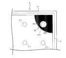
- FIG. 3 is a partial front view of the display device according to Embodiment 1.
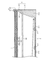
- FIG. 4 is a sectional view taken along line IV-IV in FIG. 3.
- FIG. 5 is a sectional view taken along line VV in FIG. 3.
- 6 is a partial front view of a display device according to Embodiment 2.
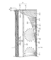
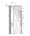
- FIG. 7 is a sectional view taken along line VII-VII in FIG. 6.
- FIG. 7 is a sectional view taken along line VII-VII in FIG. 6. It is a front view which shows the 1st modification of a reflection member.
- FIG. 6 is a partial front view of a display device according to Embodiment 3.
- FIG. FIG. 12 is a cross-sectional view taken along line XII-XII in FIG. 11.
- FIG. 1 is an exploded perspective view of the display device according to the first embodiment
- FIG. 2 is a longitudinal sectional view of the display device according to the first embodiment.
- the display device according to the present embodiment is, for example, a liquid crystal display device including a liquid crystal panel 1 on the front side of the device and a light source unit 2 on the back side of the device.
- the liquid crystal panel 1 is a rectangular display panel that includes a plurality of liquid crystal display elements arranged in a matrix and displays an image on the front of the panel.
- the light source unit 2 is a direct type backlight device that emits light from the back side of the liquid crystal panel 1.
- the light source unit 2 includes a light emitting diode (LED) substrate 21, a diffusion plate 22, and an optical sheet 23. Light emitted from the light source (LED chip 211) of the LED substrate 21 is transmitted via the diffusion plate 22 and the optical sheet 23. Then, the liquid crystal panel 1 is irradiated.
- LED light emitting diode
- the LED substrate 21 includes a rectangular substrate 210 and a plurality of LED chips 211, 211,..., 211 mounted at substantially equal intervals along the longitudinal direction and the short direction of the substrate 210.
- the LED chip 211 is, for example, a package of a light-emitting diode element, a phosphor that covers the light-emitting diode element, and a container that houses them.
- Reflecting members 24, 24, 24, 24 are provided around the LED chips 211, 211, 211, 211 adjacent to the four corners of the liquid crystal panel 1, respectively.
- a reflective sheet 212 having high reflectivity is provided on the surface of the LED substrate 21.
- the diffusion plate 22 is formed of a synthetic resin such as acrylic resin or polycarbonate resin having high transparency, and is a rectangular plate having a predetermined thickness.
- the diffusion plate 22 includes a large number of diffusion particles dispersed inside and has a function of diffusing transmitted light. That is, the light from the LED chip 211 incident from one surface of the diffusion plate 22 is diffused by the internal diffusion particles when transmitted in the thickness direction, and a part thereof is directed to the other surface side (device front side) of the diffusion plate 22. The light is transmitted, and the remaining part is reflected to one surface side (device back side) of the diffusion plate 22.
- the optical sheet 23 is a translucent sheet having predetermined optical characteristics, and is composed of a laminate of a plurality of sheets.
- the optical sheet 23 is formed as a laminate of a diffusion sheet 23a, a lens sheet 23b, and a reflective polarizing sheet 23c. Note that the number and configuration of the sheets included in the optical sheet 23 can be appropriately changed according to required luminance specifications, optical characteristics, and the like.
- the display device includes a panel chassis 3 that houses the LED substrate 21.
- the panel chassis 3 includes a rear-side panel chassis 31 that is a shallow housing and a front-side panel chassis 32 that is a frame-like frame having an opening in the center.
- the rear panel chassis 31 includes a rectangular bottom surface portion 311 to which the LED substrate 21 on which the LED chip 211 is mounted is attached, and a side wall portion 312 that rises vertically from the edge of the bottom surface portion 311.
- the back side panel chassis 31 is formed of a metal such as aluminum having excellent thermal conductivity, for example, in order to dissipate heat generated from the LED chip 211.
- the inner peripheral surface of the side wall portion 312 is an inclined surface that is inclined obliquely outward between the bottom surface portion 311 and the diffusion plate 22 (that is, a tapered shape in which the thickness of the side wall portion 312 gradually decreases in the height direction). And is configured to reflect incident light to the front side of the apparatus.
- the inclined surface is preferably formed of a reflector having a light reflectance of 85% or more, for example.
- the structure which provides a highly reflective reflective sheet in an inclined surface may be sufficient, and it is good also as a structure which apply
- the front-side panel chassis 32 is a frame-like frame body having an opening in the center portion and including four peripheral wall portions 321, and diffuses by sandwiching the periphery of the diffusion plate 22 with the back-side panel chassis 31.
- the plate 22 is configured to be supported.
- the inner peripheral surface of the peripheral wall portion 321 is an inclined surface that is inclined outwardly between the diffusion plate 22 and the optical sheet 23 (that is, a tapered shape in which the thickness of the peripheral wall portion 321 gradually decreases in the height direction). And is configured to reflect incident light to the front side of the apparatus.
- the inclined surface is preferably formed of a reflector having a light reflectance of 85% or more, for example.
- the structure which provides a highly reflective reflective sheet in an inclined surface may be sufficient, and it is good also as a structure which apply
- the display device also includes a frame-like bezel 4 that covers the periphery of the liquid crystal panel 1 from the front side of the device.
- the bezel 4 is a frame that has an opening at the center and is slightly larger than the panel chassis 3.
- the frame portion 41 covers the periphery of the liquid crystal panel 1 from the front, and the side wall portion 42 covers the outer peripheral surface of the panel chassis 3. Is provided.
- the frame The inner peripheral surface of the portion 41 abuts on the front side periphery of the liquid crystal panel 1, and the inner peripheral surface of the side wall portion 42 abuts on the outer peripheral surfaces of the back side panel chassis 31 and the front side panel chassis 32. Therefore, the liquid crystal panel 1 is supported in a state of being sandwiched between the frame portion 41 of the bezel 4 and the front panel chassis 32 together with the optical sheet 23.
- the display device is configured.
- the display device irradiates light from the back side of the liquid crystal panel 1 using the light source unit 2 and drives and controls the liquid crystal display elements arranged on the liquid crystal panel 1 by a drive circuit not shown in the figure.
- Image display is performed by adjusting the light transmittance in the display element (each pixel).
- FIG. 3 is a partial front view of the display device according to Embodiment 1
- FIG. 4 is a cross-sectional view taken along line IV-IV in FIG. 3
- FIG. 5 is a cross-sectional view taken along line VV in FIG.
- the reflecting member 24 is provided around the LED chip 211 close to the four corners of the liquid crystal panel 1.
- the LED chips 211, 211,..., 211 are mounted at substantially equal intervals along the longitudinal direction and the short direction of the substrate 210, these LED chips 211, 211,.
- the reflecting member 24 is provided around each of the four LED chips 211, 211, 211, 211 arranged at the four corners.
- the reflecting member 24 has a reflecting surface in a range of 90 to 270 degrees (for example, a range of 135 to 225 degrees) with respect to a straight line connecting the light source center of the LED chip 211 and the four corners of the substrate 210. 241. As shown in FIG. 5, the reflecting surface 241 is configured by an inclined surface that is inclined so that the height from the LED substrate 210 increases toward the corner.
- the reflecting surface 241 of the reflecting member 24 reflects the light emitted from the LED chips 211, 211,..., 211 and diffused by the diffusion plate 22 or the optical sheet 23 toward the four corners of the liquid crystal panel 1 closest to itself. To do. For this reason, it is preferable that the whole reflection member 24 (or the reflection surface 241 in the reflection member 24) is formed of a reflector having a light reflectance of 85% or more, for example. In addition, a configuration in which a highly reflective reflective sheet is provided on the reflective surface 241 may be used, and a configuration in which a white paint is applied to the reflective surface 241 may be employed.
- the diffusion plate 22 diffuses the light by the internal diffusion particles, so that the in-plane luminance distribution of the light transmitted to the liquid crystal panel 1 side is made uniform. It has a function to do.
- the distance from the light source such as an LED to the panel chassis is longer in the diagonal direction than the vertical direction or the horizontal direction, so the light amount decreases in the four corner areas of the panel, and the area other than the four corners. Compared to the above, the darkness tends to stand out.
- the reflecting member 24 is provided around the LED chip 211 adjacent to the four corners of the liquid crystal panel 1, the light is emitted from the LED chip 211 toward the four corners of the liquid crystal panel 1. Not only the light but also the light diffused by the diffusion plate 22 or the optical sheet 23 and originally toward the four corners of the inner peripheral surface of the rear panel chassis 31 reach the four corners of the liquid crystal panel 1.
- the amount of light reaching the four corners of the liquid crystal panel 1 is relatively increased as compared with the case where the reflecting member 24 is not present, so that the amount of light near the four corners of the liquid crystal panel 1 is reduced. Therefore, the uniformity of the luminance distribution in the surface of the liquid crystal panel 1 can be improved.
- a display device with a narrow frame that cannot sufficiently cover the peripheral edge of the panel can ensure the uniformity of the luminance distribution in the effective display screen.
- dark portions do not stand out in the four corner areas where the plurality of display devices are abutted.
- the reflecting member 24 is provided around the LED chips 211, 211, 211, 211 arranged at the four corners.
- the place where the reflecting member 24 is provided depends on the arrangement method of the LED chips 211. It can be changed as appropriate. For example, when there are two or more LED chips 211 having a minimum separation distance from one corner of the liquid crystal panel 1, reflective members 24, 24,... Are provided around these LED chips 211, 211,. It is good also as a structure.
- the reflection surface 241 is provided in the range of 90 to 270 degrees (for example, the range of 135 to 225 degrees) with respect to the straight line connecting the light source center of the LED chip 211 and the four corners of the substrate 210.
- the member 24 has been described, the shape of the reflecting member 24 is not limited to the shape described in the first embodiment.
- the second embodiment a configuration in which the reflecting member 25 arranged so as to surround the LED chip 211 will be described. Note that the overall configuration of the display device is the same as that of Embodiment 1, and thus description thereof is omitted.
- FIGS. 7 and 8 are cross-sectional views taken along the line VII-VII in FIG.
- the reflecting member 25 is provided around the LED chip 211 close to the four corners of the liquid crystal panel 1.
- the reflecting member 25 according to the second embodiment is a fan-shaped member when viewed from the front, and houses the reflecting surface 251 inclined so that the height from the LED substrate 210 increases toward the corner and the LED chip 211. And an accommodating portion 252 to be provided.
- the accommodating portion 252 is formed by cutting the reflecting member 25 into a cylindrical shape or an elliptical column shape, and is configured not to block light emitted from the accommodated LED chip 211 (see FIG. 7).
- the reflection surface 251 of the reflection member 25 reflects the light emitted from the LED chips 211, 211,..., 211 and diffused by the diffusion plate 22 or the optical sheet 23 toward the four corners of the liquid crystal panel 1 closest to itself. .
- the whole reflection member 25 (or the reflection surface 251 in the reflection member 25) is formed of a reflector having a light reflectance of 85% or more, for example.
- a configuration in which a highly reflective reflective sheet is provided on the reflective surface 251 may be used, and a configuration in which a white paint is applied to the reflective surface 251 may be employed.
- the reflecting member 25 since the reflecting member 25 is provided, as shown in FIG. 8, light incident at a relatively shallow angle with respect to the reflecting surface 251 can be reflected toward the four corners of the liquid crystal panel 1. Light incident at a relatively deep angle with respect to the reflection surface 251 can be reflected slightly to the near side from the four corners of the liquid crystal panel 1. Note that the width of the reflecting member 25, the angle range in which the reflecting surface 251 is provided, the height of the reflecting member 25 from the surface of the substrate 210, the inclination angle of the reflecting surface 251 and the accommodation position of the LED chip 211 are the four corners of the liquid crystal panel 1. Can be changed as appropriate according to the required brightness, uniformity of light quantity, and the like.
- the diffusion plate 22 diffuses the light by the internal diffusion particles, so that the in-plane luminance distribution of the light transmitted to the liquid crystal panel 1 side is made uniform. It has a function to do.
- the distance from the light source such as an LED to the panel chassis is longer in the diagonal direction than the vertical direction or the horizontal direction, so the light amount decreases in the four corner areas of the panel, and the area other than the four corners. Compared to the above, the darkness tends to stand out.
- the reflecting member 25 is provided around the LED chip 211 adjacent to the four corners of the liquid crystal panel 1, the light is emitted from the LED chip 211 toward the four corners of the liquid crystal panel 1. Not only the light but also the light diffused by the diffusion plate 22 or the optical sheet 23 and originally toward the four corners of the inner peripheral surface of the rear panel chassis 31 reach the four corners of the liquid crystal panel 1.
- the amount of light reaching the four corners of the liquid crystal panel 1 is relatively increased as compared with the case where the reflecting member 25 is not present, so that the amount of light near the four corners of the liquid crystal panel 1 is reduced. Therefore, the uniformity of the luminance distribution in the surface of the liquid crystal panel 1 can be improved.
- the shape of the reflecting member 25 is not limited to that shown in FIG.
- FIG. 9 is a front view showing a first modification of the reflecting member 25.
- the reflection member 25 shown in FIG. 9 includes a reflection surface 251 that is inclined so that the height from the LED substrate 210 increases toward the corner, and a storage portion 252 that stores the LED chip 211, as described above. ing.
- the reflecting member 25 shown in FIG. 9 has a shape obtained by dividing a circle into four equal parts when viewed from the front (a sector having a central angle of 90 degrees), and has a larger area of the reflecting surface 251 than that shown in FIG. Therefore, the amount of light reaching the four corners of the liquid crystal panel 1 can be increased.
- FIG. 10 is a front view showing a second modification of the reflecting member 25. Similar to the above, the reflecting member 25 shown in FIG. 10 includes a reflecting surface 251 that is inclined so that the height from the LED substrate 210 increases toward the corner, and a housing portion 252 that houses the LED chip 211. ing.
- the reflecting member 25 shown in FIG. 10 has a shape in which a square is cut out in a fan shape when viewed from the front.
- the area of the reflecting surface 251 is increased as compared with that shown in FIG. 6, and the light toward the peripheral edges near the four corners of the substrate 210 can be reflected to the four corners of the liquid crystal panel 1. The amount of light reaching the four corners of the liquid crystal panel 1 can be increased.
- FIG. 11 is a partial front view of the display device according to Embodiment 3
- FIG. 12 is a cross-sectional view taken along line XII-XII in FIG.
- the reflecting members 313 are provided at the four corners of the inner peripheral surface of the back side panel chassis 31.
- the reflection member 313 is formed integrally with the rear panel chassis 31 and includes an inclined surface that is inclined so that the height from the LED substrate 210 increases toward the corner.
- the inclination angle of the inclined surface is adjusted to reflect the incident light to the four corners of the liquid crystal panel 1, and has an angle different from the inclination angle of the inner peripheral surface of the side wall portion 312 other than the four corners.
- the reflective member 313 reflects light emitted from the LED chips 211, 211, ..., 211 and diffused by the diffusion plate 22 or the optical sheet 23 toward the four corners of the liquid crystal panel 1 closest to itself. For this reason, it is preferable that the reflection member 313 is formed of a reflector having a light reflectance of 85% or more, for example. Moreover, the structure which provides a highly reflective reflective sheet in the reflective surface in the reflective member 313 may be sufficient, and it is good also as a structure which apply
- the diffusion plate 22 diffuses the light by the internal diffusion particles, so that the in-plane luminance distribution of the light transmitted to the liquid crystal panel 1 side is made uniform. It has a function to do.
- the distance from the light source such as an LED to the panel chassis is longer in the diagonal direction than the vertical direction or the horizontal direction, so the light amount decreases in the four corner areas of the panel, and the area other than the four corners. Compared to the above, the darkness tends to stand out.
- the reflecting members 313 are provided at the four corners on the inner peripheral surface of the back side panel chassis 35, only the light emitted from the LED chip 211 toward the four corners of the liquid crystal panel 1 is used. However, the light that is diffused by the diffusion plate 22 or the optical sheet 23 and goes toward the four corners of the inner peripheral surface of the rear panel chassis 31 originally reaches the four corners of the liquid crystal panel 1.
- the amount of light reaching the four corners of the liquid crystal panel 1 is relatively increased as compared with the case where the reflecting member 313 is not present, so that the decrease in the amount of light near the four corners of the liquid crystal panel 1 is suppressed. And the uniformity of the luminance distribution in the plane of the liquid crystal panel 1 can be improved.
Landscapes
- Physics & Mathematics (AREA)
- Nonlinear Science (AREA)
- Mathematical Physics (AREA)
- Chemical & Material Sciences (AREA)
- Crystallography & Structural Chemistry (AREA)
- General Physics & Mathematics (AREA)
- Optics & Photonics (AREA)
- Planar Illumination Modules (AREA)
- Liquid Crystal (AREA)
Abstract
表示面内における輝度分布の均一性を高めることができる表示装置の提供。 一面に画像が表示される矩形状の表示パネルと、前記一面と対向する表示パネルの他面に対向配置され、複数の光源が実装された基板と、表示パネルと基板との間に配置される拡散板と、光源からの光が通過する開口を有し、拡散板の周縁を支持する支持部材とを備える表示装置において、表示パネルの四隅部に近接する各光源の周囲に夫々設けられ、拡散板にて拡散した光を表示パネルの隅部へ反射させる反射部材を備える。
Description
本発明は、直下型のバックライトを備えた表示装置に関する。
近年、液晶パネルを画像表示部として備える表示装置が広く普及している。この表示装置は、液晶パネルの背面側にバックライトを配して構成されている。
バックライトは、種々の形式で採用され、液晶パネルの背面全体に対向する位置に光源を配置する直下型がその一つの形式として採用されている。例えば、特許文献1には、上面に開口部を有する扁平な筐体内に円筒光源及び反射体を配すと共に、筐体の開口部に光透過拡散体を配設したバックライト装置が開示されている。
このようなバックライト装置を備えた表示装置は、光源からの光を光透過拡散体により拡散し、拡散した光を液晶パネルにより変調して透過させ、液晶パネルの正面に画像を表示する。
上述した特許文献1では、筐体の内面に底面部と側面部とで反射性能が異なる反射体を設けることにより、照光面における輝度の低い部分の光量と輝度の高い部分の光量を平均化して輝度ムラを軽減することができるとしている。
しかしながら、特許文献1に開示されたバックライト装置では、筐体の側面部にて反射された光は照光面内の内側の領域へ導かれるため、照光面の四隅部分では十分な輝度が得られないという問題点を有している。
本発明は、斯かる事情に鑑みてなされたものであり、表示面内における輝度分布の均一性を高めることができる表示装置を提供することを目的とする。
本願の表示装置は、一面に画像が表示される矩形状の表示パネルと、前記一面と対向する前記表示パネルの他面に対向配置され、複数の光源が実装された基板と、前記表示パネルと前記基板との間に配置される拡散板と、前記光源からの光が通過する開口を有し、前記拡散板の周縁を支持する支持部材とを備える表示装置において、前記表示パネルの四隅部に近接する各光源の周囲に夫々設けられ、前記拡散板にて拡散した光を前記表示パネルの隅部へ反射させる反射部材を備えることを特徴とする。
本願によれば、表示面内における輝度分布の均一性を高めることができる。
以下、本発明をその実施の形態を示す図面に基づいて具体的に説明する。
(実施の形態1)
図1は実施の形態1に係る表示装置の分解斜視図であり、図2は実施の形態1に係る表示装置の縦断面図である。本実施の形態に係る表示装置は、例えば、装置正面側に液晶パネル1を備え、装置背面側に光源部2を備えた液晶表示装置である。
(実施の形態1)
図1は実施の形態1に係る表示装置の分解斜視図であり、図2は実施の形態1に係る表示装置の縦断面図である。本実施の形態に係る表示装置は、例えば、装置正面側に液晶パネル1を備え、装置背面側に光源部2を備えた液晶表示装置である。
液晶パネル1は、マトリクス状に配列された複数の液晶表示素子を備え、パネル正面に画像を表示する矩形状の表示パネルである。
光源部2は、液晶パネル1の背面側から光を照射する直下型のバックライト装置である。光源部2は、LED(Light Emitting Diode)基板21、拡散板22、及び光学シート23を備え、LED基板21の光源(LEDチップ211)が出射する光を、拡散板22及び光学シート23を介して、液晶パネル1に照射する。
LED基板21は、矩形状の基板210と、基板210の長手方向及び短手方向に沿ってそれぞれ略等間隔に実装された複数のLEDチップ211,211,…,211とを備える。LEDチップ211は、例えば、発光ダイオード素子と、当該発光ダイオード素子を覆う蛍光体と、これらを収容する収容体とをパッケージ化したものである。また、液晶パネル1の四隅部に近接するLEDチップ211,211,211,211の周囲には、それぞれ反射部材24,24,24,24が設けられている。更に、LED基板21の表面には、高反射性を有する反射シート212が設けられている。
拡散板22は、透明度が高いアクリル樹脂、ポリカーボネート樹脂等の合成樹脂により形成されており、所定の厚みを有する矩形状の板体である。拡散板22は、内部に分散配置された多数の拡散粒子を備え、透過する光を拡散させる機能を有する。すなわち、拡散板22の一面から入射するLEDチップ211からの光は、厚み方向へ透過する際に内部の拡散粒子によって拡散され、その一部は拡散板22の他面側(装置正面側)へ透過し、残りの一部は拡散板22の一面側(装置背面側)へ反射する。
光学シート23は、所定の光学特性を有する透光性のシートであり、複数のシートの積層体により構成されている。本実施の形態では、光学シート23は、拡散シート23a、レンズシート23b、及び反射型偏光シート23cの積層体として形成されている。なお、光学シート23が備えるシートの枚数及び構成は、要求される輝度仕様や光学特性などに応じて適宜変更することが可能である。
表示装置は、LED基板21を収容するパネルシャーシ3を備える。本実施の形態では、パネルシャーシ3は、浅底の筐体である背面側パネルシャーシ31と、中央部に開口を有する額縁状の枠体である正面側パネルシャーシ32とを備える。
背面側パネルシャーシ31は、LEDチップ211が実装されたLED基板21が取り付けられる矩形状の底面部311と、底面部311の縁辺から垂直に立ち上がる側壁部312とを備える。背面側パネルシャーシ31は、LEDチップ211から発せられる熱を放熱するために、例えば熱伝導性に優れたアルミニウム等の金属により形成される。また、側壁部312の内周面は、底面部311と拡散板22との間で斜め外側に傾斜する傾斜面(すなわち、側壁部312の厚みが、高さ方向に徐々に薄くなるテーパー状の傾斜面)となっており、入射した光を装置正面側へ反射するように構成されている。このため、傾斜面は、例えば光反射率が85%以上の反射体により形成されていることが好ましい。また、傾斜面に高反射性の反射シートを設ける構成であってもよく、反射面に白色系の塗料を塗布する構成としてもよい。
正面側パネルシャーシ32は、中央部に開口を有し、4つの周壁部321からなる額縁状の枠体であり、背面側パネルシャーシ31との間で拡散板22の周縁を挟み込むことにより、拡散板22を支持するように構成されている。また、周壁部321の内周面は、拡散板22と光学シート23との間で斜め外側に傾斜した傾斜面(すなわち、周壁部321の厚みが、高さ方向に徐々に薄くなるテーパー状の傾斜面)となっており、入射した光を装置正面側へ反射するように構成されている。このため、傾斜面は、例えば光反射率が85%以上の反射体により形成されていることが好ましい。また、傾斜面に高反射性の反射シートを設ける構成であってもよく、反射面に白色系の塗料を塗布する構成としてもよい。
また、表示装置は、液晶パネル1の周縁を装置正面側から覆う額縁状のベゼル4を備える。ベゼル4は、中央部に開口を有し、パネルシャーシ3より少しだけ大きい枠体であり、液晶パネル1の周縁を正面から覆う額縁部41と、パネルシャーシ3の外周面を覆う側壁部42とを備える。背面側パネルシャーシ31と正面側パネルシャーシ32との間で拡散板22を挟み込み、正面側パネルシャーシ32に光学シート23及び液晶パネル1を載置した状態にて、ベゼル4を取り付けた場合、額縁部41の内周面は液晶パネル1の正面側周縁に当接し、側壁部42の内周面は背面側パネルシャーシ31及び正面側パネルシャーシ32の外周面に当接する。よって、液晶パネル1は、光学シート23と共に、ベゼル4の額縁部41と正面側パネルシャーシ32とにより挟持された状態にて支持される。
以上により、本実施の形態に係る表示装置が構成される。表示装置は、光源部2を用いて液晶パネル1の背面側から光を照射すると共に、液晶パネル1に配列されている各液晶表示素子を図に示していない駆動回路により駆動制御し、各液晶表示素子(各画素)における光の透過率を調整することにより、画像表示を行う。
図3は実施の形態1に係る表示装置の部分正面図、図4は図3のIV-IV線における断面図、図5は図3のV-V線における断面図である。前述したように、液晶パネル1の四隅部に近接するLEDチップ211の周囲には、反射部材24を設けている。本実施の形態では、基板210の長手方向及び短手方向に沿ってそれぞれ略等間隔にLEDチップ211,211,…,211を実装しているので、これらのLEDチップ211,211,…,211のうち、四隅に配置された4つのLEDチップ211,211,211,211の周囲にそれぞれ反射部材24を設けている。
本実施の形態では、反射部材24は、LEDチップ211の光源中心と基板210の四隅部とを結ぶ直線に対して90度から270度の範囲(例えば135度から225度の範囲)に反射面241を有している。この反射面241は、図5に示すように、隅部に向かうにつれてLED基板210からの高さが高くなるように傾斜した傾斜面により構成されている。
反射部材24の反射面241は、LEDチップ211,211,…,211から出射され、拡散板22又は光学シート23にて拡散された光を自身から最も近い液晶パネル1の四隅部の方向へ反射する。このため、反射部材24の全体(又は反射部材24における反射面241)は、例えば光反射率が85%以上の反射体により形成されていることが好ましい。また、反射面241に高反射性の反射シートを設ける構成であってもよく、反射面241に白色系の塗料を塗布する構成としてもよい。
拡散板22は、LEDチップ211,211,…,211からの光が透過する際、内部の拡散粒子によって光を拡散するので、液晶パネル1側へ透過する光の面内の輝度分布を均一化する機能を有している。しかしながら、一般的には、LED等の光源からパネルシャーシまでの距離は、縦方向又は横方向に対して、斜め方向の距離が遠いため、パネルの四隅領域では光量が減少し、四隅以外の領域と比較して相対的に暗さが目立つ傾向にある。
これに対し、本実施の形態では、液晶パネル1の四隅部に近接するLEDチップ211の周囲に反射部材24を設けているので、LEDチップ211から液晶パネル1の四隅部へ向けて出射された光だけでなく、拡散板22又は光学シート23で拡散され、本来なら背面側パネルシャーシ31の内周面における四隅部へ向かう光も液晶パネル1の四隅部に到達することになる。
よって、実施の形態1では、液晶パネル1の四隅部に到達する光量は反射部材24が存在しない場合と比較して相対的に増大するので、液晶パネル1の四隅部付近での光量の減少を抑えることができ、液晶パネル1の面内における輝度分布の均一性を高めることができる。
特に、パネルの周縁を十分に覆い隠すことができない狭額縁の表示装置であっても、有効表示画面内における輝度分布の均一性を確保することができる。また、本実施の形態に係る表示装置を複数枚並置してマルチディスプレイ装置を構成したとしても、複数枚を突き合わせた四隅領域において、暗部が目立つことがなくなる。
なお、反射部材24の幅、反射面241を設ける角度範囲、反射部材24の基板210表面からの高さ、反射面241の傾斜角度、反射部材24のLEDチップ211からの離隔距離等は、液晶パネル1の四隅部において要求される輝度に応じて適宜変更され得る。
また、本実施の形態では、四隅に配置されたLEDチップ211,211,211,211の周囲に反射部材24を設ける構成としたが、反射部材24を設ける箇所は、LEDチップ211の配置方法に応じて適宜変更することが可能である。例えば、液晶パネル1の一の隅部から離隔寸法が最小となるLEDチップ211が2つ以上存在する場合、これらのLEDチップ211,211,…の周囲にそれぞれ反射部材24,24,…を設ける構成としてもよい。
(実施の形態2)
実施の形態1では、LEDチップ211の光源中心と基板210の四隅部とを結ぶ直線に対して90度から270度の範囲(例えば135度から225度の範囲)に反射面241を備えた反射部材24について説明したが、反射部材24の形状は実施の形態1に記載の形状に限定されるものではない。
実施の形態2では、LEDチップ211を取り囲むように配置された反射部材25を設けた構成について説明する。なお、表示装置の全体構成は実施の形態1と同様であるため、その説明を省略することとする。
実施の形態1では、LEDチップ211の光源中心と基板210の四隅部とを結ぶ直線に対して90度から270度の範囲(例えば135度から225度の範囲)に反射面241を備えた反射部材24について説明したが、反射部材24の形状は実施の形態1に記載の形状に限定されるものではない。
実施の形態2では、LEDチップ211を取り囲むように配置された反射部材25を設けた構成について説明する。なお、表示装置の全体構成は実施の形態1と同様であるため、その説明を省略することとする。
図6は実施の形態2に係る表示装置の部分正面図、図7及び図8は図6のVII-VII線における断面図である。実施の形態2では、実施の形態1と同様に、液晶パネル1の四隅部に近接するLEDチップ211の周囲に反射部材25を設けている。実施の形態2に係る反射部材25は、正面視で扇形をなす部材であり、隅部に向かうにつれてLED基板210からの高さが高くなるように傾斜した反射面251と、LEDチップ211を収容する収容部252とを備えている。
収容部252は、反射部材25を円柱状又は楕円柱状に切り欠くことによって形成され、収容しているLEDチップ211から出射される光を遮らないように構成されている(図7を参照)。
反射部材25の反射面251は、LEDチップ211,211,…,211から出射され、拡散板22又は光学シート23にて拡散された光を自身から最も近い液晶パネル1の四隅の方向へ反射する。このため、反射部材25の全体(又は反射部材25における反射面251)は、例えば光反射率が85%以上の反射体により形成されていることが好ましい。また、反射面251に高反射性の反射シートを設ける構成であってもよく、反射面251に白色系の塗料を塗布する構成としてもよい。
本実施の形態では、反射部材25を備えるため、図8に示すように、反射面251に対して比較的浅い角度で入射する光を液晶パネル1の四隅部の方向へ反射することができ、反射面251に対して比較的深い角度で入射する光を液晶パネル1の四隅部より少し手前側に反射することができる。なお、反射部材25の幅、反射面251を設ける角度範囲、反射部材25の基板210表面からの高さ、反射面251の傾斜角度、LEDチップ211の収容位置等は、液晶パネル1の四隅部において要求される輝度や光量の均一性等に応じて適宜変更され得る。
拡散板22は、LEDチップ211,211,…,211からの光が透過する際、内部の拡散粒子によって光を拡散するので、液晶パネル1側へ透過する光の面内の輝度分布を均一化する機能を有している。しかしながら、一般的には、LED等の光源からパネルシャーシまでの距離は、縦方向又は横方向に対して、斜め方向の距離が遠いため、パネルの四隅領域では光量が減少し、四隅以外の領域と比較して相対的に暗さが目立つ傾向にある。
これに対し、本実施の形態では、液晶パネル1の四隅部に近接するLEDチップ211の周囲に反射部材25を設けているので、LEDチップ211から液晶パネル1の四隅部へ向けて出射された光だけでなく、拡散板22又は光学シート23で拡散され、本来なら背面側パネルシャーシ31の内周面における四隅部へ向かう光も液晶パネル1の四隅部に到達することになる。
よって、実施の形態2においても、液晶パネル1の四隅部に到達する光量は反射部材25が存在しない場合と比較して相対的に増大するので、液晶パネル1の四隅付近での光量の減少を抑えることができ、液晶パネル1の面内における輝度分布の均一性を高めることができる。
なお、反射部材25の形状は図6に示すものに限定されない。図9は反射部材25の第1変形例を示す正面図である。図9に示す反射部材25は、前述と同様に、隅部に向かうにつれてLED基板210からの高さが高くなるように傾斜した反射面251と、LEDチップ211を収容する収容部252とを備えている。図9に示す反射部材25は、正面視で円を四等分した形状(中心角が90度の扇形)を有しており、図6に示すものと比較して反射面251の面積を大きくしているので、液晶パネル1の四隅部へ到達する光量を増大させることができる。
図10は反射部材25の第2変形例を示す正面図である。図10に示す反射部材25は、前述と同様に、隅部に向かうにつれてLED基板210からの高さが高くなるように傾斜した反射面251と、LEDチップ211を収容する収容部252とを備えている。図10に示す反射部材25は、正面視において、正方形を扇形に切り欠いた形状を有している。第2変形例では、図6に示すものと比較して反射面251の面積を大きくすると共に、基板210の四隅近傍の周縁に向かう光を液晶パネル1の四隅部へ反射することができるので、液晶パネル1の四隅部へ到達する光量を増大させることができる。
(実施の形態3)
実施の形態3では、拡散板22又は光学シート23で拡散された光を反射する反射部材を背面側パネルシャーシ31と一体に形成した構成について説明する。
なお、表示装置の全体構成は実施の形態1と同様であるため、その説明を省略することとする。
実施の形態3では、拡散板22又は光学シート23で拡散された光を反射する反射部材を背面側パネルシャーシ31と一体に形成した構成について説明する。
なお、表示装置の全体構成は実施の形態1と同様であるため、その説明を省略することとする。
図11は実施の形態3に係る表示装置の部分正面図、図12は図11のXII-XII線における断面図である。実施の形態3では、背面側パネルシャーシ31における内周面の四隅に反射部材313を設けている。この反射部材313は、背面側パネルシャーシ31と一体に形成されており、隅部へ向かうに連れてLED基板210からの高さが高くなるように傾斜した傾斜面を備えている。この傾斜面の傾斜角度は、入射した光を液晶パネル1の四隅部へ反射するような角度に調整されており、四隅以外の側壁部312の内周面の傾斜角度とは異なる角度を有する。
反射部材313は、LEDチップ211,211,…,211から出射され、拡散板22又は光学シート23にて拡散された光を自身から最も近い液晶パネル1の四隅部の方向へ反射する。このため、反射部材313は、例えば光反射率が85%以上の反射体により形成されていることが好ましい。また、反射部材313における反射面に高反射性の反射シートを設ける構成であってもよく、反射面に白色系の塗料を塗布する構成としてもよい。
拡散板22は、LEDチップ211,211,…,211からの光が透過する際、内部の拡散粒子によって光を拡散するので、液晶パネル1側へ透過する光の面内の輝度分布を均一化する機能を有している。しかしながら、一般的には、LED等の光源からパネルシャーシまでの距離は、縦方向又は横方向に対して、斜め方向の距離が遠いため、パネルの四隅領域では光量が減少し、四隅以外の領域と比較して相対的に暗さが目立つ傾向にある。
これに対し、本実施の形態では、背面側パネルシャーシ35の内周面における四隅に反射部材313を設けているので、LEDチップ211から液晶パネル1の四隅部へ向けて出射された光だけでなく、拡散板22又は光学シート23で拡散され、本来なら背面側パネルシャーシ31の内周面における四隅部へ向かう光も液晶パネル1の四隅部に到達することになる。
よって、実施の形態3では、液晶パネル1の四隅部に到達する光量は反射部材313が存在しない場合と比較して相対的に増大するので、液晶パネル1の四隅付近での光量の減少を抑えることができ、液晶パネル1の面内における輝度分布の均一性を高めることができる。
なお、実施の形態3では、反射部材313を背面側パネルシャーシ31と一体に形成した構成について説明したが、背面側パネルシャーシ313と別体に構成してもよい。
今回開示された実施の形態は、全ての点で例示であって、制限的なものではないと考えられるべきである。本発明の範囲は、上述した意味ではなく、請求の範囲によって示され、請求の範囲と均等の意味及び範囲内での全ての変更が含まれることが意図される。また、各実施の形態で記載されている技術的特徴は、お互いに組み合わせることが可能である。
1 液晶パネル
2 光源部
3 パネルシャーシ
4 ベゼル
21 LED基板
22 拡散板
23 光学シート
24,25,313 反射部材
31 背面側パネルシャーシ
32 正面側パネルシャーシ
211 LEDチップ
2 光源部
3 パネルシャーシ
4 ベゼル
21 LED基板
22 拡散板
23 光学シート
24,25,313 反射部材
31 背面側パネルシャーシ
32 正面側パネルシャーシ
211 LEDチップ
Claims (6)
- 一面に画像が表示される矩形状の表示パネルと、前記一面と対向する前記表示パネルの他面に対向配置され、複数の光源が実装された基板と、前記表示パネルと前記基板との間に配置される拡散板と、前記光源からの光が通過する開口を有し、前記拡散板の周縁を支持する支持部材とを備える表示装置において、
前記表示パネルの四隅部に近接する各光源の周囲に夫々設けられ、前記拡散板にて拡散した光を前記表示パネルの隅部へ反射させる反射部材
を備えることを特徴とする表示装置。 - 前記表示パネルの四隅部から離隔寸法が夫々最小となる少なくとも4つの光源の周囲に前記反射部材を設けてある
ことを特徴とする請求項1に記載の表示装置。 - 前記反射部材は、前記隅部へ向かうにつれて前記基板からの高さが高くなるように傾斜した傾斜面を備え、
前記拡散板にて拡散した光を前記傾斜面により反射する
ことを特徴とする請求項1又は請求項2に記載の表示装置。 - 前記反射部材は、前記光源を収容する収容部を備える
ことを特徴とする請求項1から請求項3の何れか1つに記載の表示装置。 - 前記反射部材は、前記支持部材と一体に形成されている
ことを特徴とする請求項1から請求項3の何れか1つに記載の表示装置。 - 前記反射部材は、85%以上の光反射率を有する
ことを特徴とする請求項1から請求項5の何れか1つに記載の表示装置。
Priority Applications (3)
| Application Number | Priority Date | Filing Date | Title |
|---|---|---|---|
| CN201680082384.3A CN108700774A (zh) | 2016-02-22 | 2016-02-22 | 显示装置 |
| US16/078,857 US10712612B2 (en) | 2016-02-22 | 2016-02-22 | Display device |
| PCT/JP2016/055103 WO2017145240A1 (ja) | 2016-02-22 | 2016-02-22 | 表示装置 |
Applications Claiming Priority (1)
| Application Number | Priority Date | Filing Date | Title |
|---|---|---|---|
| PCT/JP2016/055103 WO2017145240A1 (ja) | 2016-02-22 | 2016-02-22 | 表示装置 |
Publications (1)
| Publication Number | Publication Date |
|---|---|
| WO2017145240A1 true WO2017145240A1 (ja) | 2017-08-31 |
Family
ID=59685034
Family Applications (1)
| Application Number | Title | Priority Date | Filing Date |
|---|---|---|---|
| PCT/JP2016/055103 Ceased WO2017145240A1 (ja) | 2016-02-22 | 2016-02-22 | 表示装置 |
Country Status (3)
| Country | Link |
|---|---|
| US (1) | US10712612B2 (ja) |
| CN (1) | CN108700774A (ja) |
| WO (1) | WO2017145240A1 (ja) |
Cited By (1)
| Publication number | Priority date | Publication date | Assignee | Title |
|---|---|---|---|---|
| CN112823308A (zh) * | 2018-10-05 | 2021-05-18 | 微软技术许可有限责任公司 | 经光学校准的背光单元内部支撑件 |
Families Citing this family (2)
| Publication number | Priority date | Publication date | Assignee | Title |
|---|---|---|---|---|
| CN115943269A (zh) * | 2020-08-07 | 2023-04-07 | 美蓓亚三美株式会社 | 面状照明装置 |
| EP4328638B1 (en) * | 2021-10-27 | 2026-04-08 | Samsung Electronics Co., Ltd. | Display device |
Citations (6)
| Publication number | Priority date | Publication date | Assignee | Title |
|---|---|---|---|---|
| JP2002169479A (ja) * | 2000-12-04 | 2002-06-14 | Tama Electric Co Ltd | バックライト装置 |
| JP2006059606A (ja) * | 2004-08-18 | 2006-03-02 | Sony Corp | バックライト装置 |
| US20070230206A1 (en) * | 2006-04-04 | 2007-10-04 | Au Optronics Corp. | Direct Backlight Module |
| JP2008145655A (ja) * | 2006-12-08 | 2008-06-26 | Sony Corp | 液晶表示装置 |
| JP2009164026A (ja) * | 2008-01-09 | 2009-07-23 | Epson Imaging Devices Corp | 照明ユニット、液晶装置及び電子機器 |
| JP2012243653A (ja) * | 2011-05-20 | 2012-12-10 | Sharp Corp | バックライト装置および表示装置 |
Family Cites Families (2)
| Publication number | Priority date | Publication date | Assignee | Title |
|---|---|---|---|---|
| WO2017104081A1 (ja) * | 2015-12-18 | 2017-06-22 | 堺ディスプレイプロダクト株式会社 | 表示装置 |
| KR102461530B1 (ko) * | 2017-11-13 | 2022-10-31 | 엘지디스플레이 주식회사 | 이형 액정표시장치 |
-
2016
- 2016-02-22 CN CN201680082384.3A patent/CN108700774A/zh active Pending
- 2016-02-22 US US16/078,857 patent/US10712612B2/en active Active
- 2016-02-22 WO PCT/JP2016/055103 patent/WO2017145240A1/ja not_active Ceased
Patent Citations (6)
| Publication number | Priority date | Publication date | Assignee | Title |
|---|---|---|---|---|
| JP2002169479A (ja) * | 2000-12-04 | 2002-06-14 | Tama Electric Co Ltd | バックライト装置 |
| JP2006059606A (ja) * | 2004-08-18 | 2006-03-02 | Sony Corp | バックライト装置 |
| US20070230206A1 (en) * | 2006-04-04 | 2007-10-04 | Au Optronics Corp. | Direct Backlight Module |
| JP2008145655A (ja) * | 2006-12-08 | 2008-06-26 | Sony Corp | 液晶表示装置 |
| JP2009164026A (ja) * | 2008-01-09 | 2009-07-23 | Epson Imaging Devices Corp | 照明ユニット、液晶装置及び電子機器 |
| JP2012243653A (ja) * | 2011-05-20 | 2012-12-10 | Sharp Corp | バックライト装置および表示装置 |
Cited By (1)
| Publication number | Priority date | Publication date | Assignee | Title |
|---|---|---|---|---|
| CN112823308A (zh) * | 2018-10-05 | 2021-05-18 | 微软技术许可有限责任公司 | 经光学校准的背光单元内部支撑件 |
Also Published As
| Publication number | Publication date |
|---|---|
| CN108700774A (zh) | 2018-10-23 |
| US10712612B2 (en) | 2020-07-14 |
| US20200133076A1 (en) | 2020-04-30 |
Similar Documents
| Publication | Publication Date | Title |
|---|---|---|
| TWI325988B (ja) | ||
| JP7770455B2 (ja) | 発光装置、表示装置および照明装置 | |
| CN103189680B (zh) | 照明装置、显示装置以及电视接收装置 | |
| KR101419369B1 (ko) | 백라이트 장치 | |
| US20200379298A1 (en) | Lighting device and liquid crystal display apparatus | |
| CN105706156B (zh) | 照明设备 | |
| JP6580161B2 (ja) | 表示装置 | |
| WO2017138080A1 (ja) | 表示装置 | |
| JP2021072281A (ja) | 光源装置、照明装置、及び表示装置 | |
| US10712612B2 (en) | Display device | |
| JP2012243653A (ja) | バックライト装置および表示装置 | |
| KR102180687B1 (ko) | 디스플레이 장치 | |
| JPWO2017104081A1 (ja) | 表示装置 | |
| JP6177330B2 (ja) | 光源装置及び表示装置 | |
| KR102172170B1 (ko) | 디스플레이 기기 | |
| JP2013182854A (ja) | 照明装置及びそれを備えた表示装置 | |
| JP5713416B2 (ja) | 照明装置、シーリングライト、バックライト、液晶表示装置、及びテレビジョン受信装置 | |
| JP2003279971A (ja) | 液晶表示装置 | |
| JP2024076463A (ja) | 照明装置、及び表示装置 | |
| JP2008216372A (ja) | 光学板 | |
| KR20180138233A (ko) | 백라이트 장치 |
Legal Events
| Date | Code | Title | Description |
|---|---|---|---|
| NENP | Non-entry into the national phase |
Ref country code: DE |
|
| 121 | Ep: the epo has been informed by wipo that ep was designated in this application |
Ref document number: 16891399 Country of ref document: EP Kind code of ref document: A1 |
|
| 122 | Ep: pct application non-entry in european phase |
Ref document number: 16891399 Country of ref document: EP Kind code of ref document: A1 |
|
| NENP | Non-entry into the national phase |
Ref country code: JP |