WO2017130366A1 - パターン計測装置及びコンピュータープログラム - Google Patents
パターン計測装置及びコンピュータープログラム Download PDFInfo
- Publication number
- WO2017130366A1 WO2017130366A1 PCT/JP2016/052561 JP2016052561W WO2017130366A1 WO 2017130366 A1 WO2017130366 A1 WO 2017130366A1 JP 2016052561 W JP2016052561 W JP 2016052561W WO 2017130366 A1 WO2017130366 A1 WO 2017130366A1
- Authority
- WO
- WIPO (PCT)
- Prior art keywords
- pattern
- patterns
- measurement value
- layer
- measurement
- Prior art date
- Legal status (The legal status is an assumption and is not a legal conclusion. Google has not performed a legal analysis and makes no representation as to the accuracy of the status listed.)
- Ceased
Links
Images







Classifications
-
- G—PHYSICS
- G01—MEASURING; TESTING
- G01B—MEASURING LENGTH, THICKNESS OR SIMILAR LINEAR DIMENSIONS; MEASURING ANGLES; MEASURING AREAS; MEASURING IRREGULARITIES OF SURFACES OR CONTOURS
- G01B15/00—Measuring arrangements characterised by the use of electromagnetic waves or particle radiation, e.g. by the use of microwaves, X-rays, gamma rays or electrons
-
- H—ELECTRICITY
- H01—ELECTRIC ELEMENTS
- H01J—ELECTRIC DISCHARGE TUBES OR DISCHARGE LAMPS
- H01J37/00—Discharge tubes with provision for introducing objects or material to be exposed to the discharge, e.g. for the purpose of examination or processing thereof
- H01J37/02—Details
- H01J37/22—Optical, image processing or photographic arrangements associated with the tube
Definitions
- the present invention relates to a pattern measurement apparatus and a computer program, and more particularly to a pattern measurement apparatus and a computer program for evaluating the superposition of a periodic array pattern and a region selection pattern for selecting a part of the periodic array pattern.
- JP 2010-177500 A (corresponding U.S. Patent Publication No. US 2011/0268363)
- DSA Directed Self-Assembly
- This method uses a material in which two types of polymers, called polymer block copolymers, are synthesized and block-bonded, and is patterned using the phenomenon of self-organization due to the difference in thermodynamic properties of the two types of polymers. Is the law.
- a plurality of patterns having a pitch of 1 / N can be formed in a self-alignment manner using a pattern (guide pattern) formed by a lithography technique.
- SAMP Self Aligned Multiple Patterning
- a SiO2 film or the like is deposited on the pattern (dummy pattern) formed by the lithography technique with a CVD film and etched, only the CVD film on the side wall portion of the dummy pattern remains and the dummy pattern is removed. Is formed. By repeating this, patterns of 1/4 pitch and 1/8 pitch of the dummy pattern are formed.
- SADP Self Aligned Double Patterning
- SAQP Self Aligned Quadruple Patterning
- the pattern formed by DSA, SAMP, etc. becomes a periodic array pattern over a wide range.
- a pattern that is formed to select the area to be applied (this may be referred to as an area selection pattern) is added before or after the periodic array pattern process. To do.
- an area selection pattern is added before or after the periodic array pattern process.
- a periodic array pattern to which a device pattern is applied is formed. Since the accuracy of overlaying the periodic array pattern formed by DSA, SAMP, etc. and the region selection pattern greatly affects the performance and yield of the device, the measurement is expected to be important.
- the periodic arrangement pattern that is located is displayed on the SEM image, the periodic arrangement pattern of the other part is shielded by the region selection pattern or after the pattern is actually selected, It is difficult to confirm with an SEM image. That is, the overlapping state between the periodic array pattern and the region selection pattern is determined based on the periodic array pattern image that is visible in the opening portion of the region selection pattern or the actually selected periodic array pattern image. It is necessary to judge.
- the selected periodic array pattern changes in the number of patterns and the size and shape of the pattern located at the end depending on the state of superposition. There is no discussion about the method of evaluating the overlap between the two.
- the overlay error between the pattern formed in the first layer and the pattern formed in the second layer is determined based on the signal obtained by the charged particle beam apparatus.
- a pattern measurement apparatus having a calculation device to be obtained or a computer program for causing a computer to calculate an overlay error, wherein the calculation device is a signal obtained based on scanning of a charged particle beam with respect to a sample in which a plurality of patterns are arranged To obtain a first measurement value of the first pattern located at one end of the plurality of patterns and a second measurement value of the second pattern located at the other end of the plurality of patterns.
- a pattern meter for determining at least one of the direction of overlay displacement between the first layer and the second layer and the amount of displacement based on the comparison between the measured value and the second measured value. Apparatus, or to propose a computer program.
- the pattern formed on the first layer and the pattern formed on the second layer are overlapped based on the signal obtained by the charged particle beam apparatus.
- a pattern measuring apparatus including an arithmetic unit for obtaining an alignment error, wherein the arithmetic unit calculates the number of the plurality of patterns from a signal obtained based on scanning of a charged particle beam with respect to a sample on which a plurality of patterns are arranged.
- the number of the patterns is different from the predetermined number, the direction of overlay displacement between the first layer and the second layer and the amount of displacement based on the measurement of the plurality of patterns.
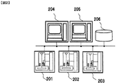
- region Schematic explanatory diagram of a measurement and inspection system in which a plurality of measurement or inspection devices are connected to a network.
- the figure explaining the overlay error measuring method in case a periodic arrangement pattern is formed by DSA.
- the figure explaining the overlay error measurement method in case a periodic arrangement pattern is formed by SAQP.
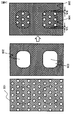
- sequence is a hole pattern.
- region is changed.
- the flowchart which shows the process at the time of performing an overlay shift
- the predetermined region is defined as a pattern based on the difference calculation and comparison between the measurement value of the first pattern on one end side and the measurement value of the second pattern disposed on the other end side of the pattern.
- Embodiments described below relate to a method, an apparatus, and a computer program for evaluating using an image of an end of an arrangement pattern in which only a predetermined area obtained by a scanning electron microscope or the like is selected.
- the present invention relates to a method, an apparatus, and a computer program that can perform overlay measurement evaluation of a periodically arranged pattern and a region selection pattern for selecting a region to which a part of the pattern is applied as a processing pattern.
- SEM is used for measurement of the processed pattern width (hereinafter referred to as “measurement”) and appearance inspection. Widely used.
- a scanning electron microscope emits an electron beam emitted from an electron source and narrowed down by a converging lens and an objective lens using a magnetic field or an interaction between an electric field and an electron beam on a sample using a deflector.
- the secondary signal (secondary electrons, reflected electrons, and electromagnetic waves) generated from the sample by electron beam irradiation is detected by a detector using the photoelectric effect, and the detection signal is synchronized with the scanning of the electron beam.
- This is an apparatus for forming a sample image by converting and processing the signal into a visible signal such as a luminance signal.
- a method for finely processing the surface of a semiconductor element, a thin film magnetic head or the like a method of forming a pattern with a fine structure such as photolithography or nanoimprint using light, an electron beam, an original plate or the like is generally used.
- the periodic array pattern forming method there is a DSA that forms a fine ordered structure using a self-organization phenomenon.
- a well-known technique in which regularly arranged holes and line and space patterns are formed on a substrate using a polymer block copolymer thin film made of polystyrene (PS) and polymethyl methacrylate (PMMA) is known. It has been.
- the shape of the periodic pattern to be formed holes or lines and spaces, etc.
- the pitch of the periodic arrangement of the shape the molecular weight, the mixing ratio, etc. Determined by.
- the first method by self-organization is to process grooves / holes on the surface of the base substrate, and to form a polymer layer containing a polymer block copolymer composition inside the groove / hole as a guide to form a regular array pattern. It is a method of forming.
- the guide is sized to be about 2 to 10 times the self-organization pattern period so that the arrangement is stable.
- the microstructure is arranged in a range limited by the guide, and the long-range order of self-organization is improved.
- the second method by self-organization is a method of chemically patterning the base substrate surface.
- regions having different affinities for each block chain constituting the polymer block copolymer are formed as a pattern.
- a region having a good chemical affinity with polystyrene is about half the self-organization cycle and is twice to ten times the self-assembly cycle. Arrange at a period of about twice.
- Other regions are chemically formed to have the same affinity as polystyrene and polymethylmethacrylate.
- the pattern by self-organization of the polymer block copolymer on the surface of this substrate is formed on the guide by using a region having good chemical affinity with polystyrene as a guide. Periodic arrangement from the pattern improves the long-range order of self-organization.
- a second method for forming a periodic array pattern there is a method called SAMP (Self Align MultiplePatterning).
- SAMP Self Align MultiplePatterning
- a film such as SiO2 is deposited by CVD and a process such as etching is performed to form a pattern having a dummy pattern of 1/2 pitch.
- the pattern layout is limited to the dummy pattern arrangement.
- the dummy pattern is often formed in a periodic arrangement, and therefore a process for deleting or selecting a part of the pattern is required.
- a third periodic array pattern forming method there is a method of performing lithography under a proof condition specialized for an array of a certain period. Furthermore, a periodic array pattern is formed by combining multiple exposures called double patterning (hereinafter referred to as DP). Since this pattern is formed by a lithography technique specialized for periodic arrangement, a process for deleting or selecting a part of the pattern is required.
- DP double patterning
- the periodic array pattern by DSA, SAMP, and DP is generated by aligning the pattern array to be formed.
- the guide and the scientific pattern and the dummy pattern on the base substrate surface are generally generated by lithography technology, and the pattern is the lower layer pattern. It is formed by measuring and adjusting the overlay. Further, the formed periodic array pattern has a deviation from the array and its dimensions due to processes after lithography.
- a process for selecting a region to be applied and forming a region selection pattern for making the device pattern is applied. ⁇ By superimposing these two patterns, a periodic array pattern that applies the device pattern is formed.
- the embodiment described below relates to an image processing method and apparatus for evaluating a process such as superposition of patterns formed mainly by the periodic arrangement pattern and the region selection pattern as described above.
- the measurement result brought about by such image processing is used for evaluation of overlay between a periodic arrangement pattern and a region selection pattern and evaluation of a technique for forming a selection region of a periodic arrangement using the region selection pattern.
- a method for measuring the overlay deviation of the relative positions and an image processing method for evaluation are proposed.
- a charged particle beam apparatus is illustrated as an apparatus for forming an image, and an example using an SEM is described as one mode thereof.
- the present invention is not limited to this.
- an ion beam is scanned over a sample.
- a focused ion beam (FIB) apparatus that forms an image may be employed as the charged particle beam apparatus.
- the type of the imaging device is not limited as long as the periodic array pattern in which the region is selected within the field of view of the captured image can be evaluated based on the image processing.
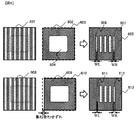
- FIG. 1 is a diagram for explaining the principle of the measurement method in this embodiment.
- Reference numeral 101 denotes a periodic arrangement pattern formed by DSA or SAMP.
- Reference numeral 102 denotes an area selection pattern for selecting an area to be a device pattern from among 101
- reference numeral 105 denotes a pattern formed by a process in which 101 and 102 are overlapped. Only the periodic arrangement pattern of the area selected in 102 becomes the pattern in 105. In general, the end of the region selection pattern is arranged between the selected region and the non-selected region.
- Reference numeral 103 denotes a relative position of the periodic arrangement pattern layer to the region selection pattern layer 102.
- the misalignment with the region selection pattern layer 102 is 0, and the shape of both ends of the selected periodic array pattern indicated by 106 and 107 is the same as the shape of the pattern inside the region. . Therefore, the line widths at both ends are the same. In this example, four periodic array lines are formed.
- FIG. 11 also illustrates a diagram equivalent to FIG. In the example of FIG. 11, only the outline 1101 of the opening of the region selection pattern is selectively shown for easy understanding.
- a contour 1101 indicates an opening of the region selection pattern in a state where the region selection pattern is appropriately superimposed on the periodic arrangement pattern 1102 that is the selected pattern.
- the lower diagram in FIG. 1 is an example in a case where a deviation of the overlay of the periodic arrangement pattern 108 and the region selection pattern 109 occurs.
- Reference numeral 110 denotes a relative position of the periodic array pattern with respect to the region selection pattern 109. In this example, five lines, one more than four desired lines, are formed due to misalignment.
- the contour 1103 shows the same state as the lower diagram of FIG.
- the overlay error is measured by using a phenomenon that there are more than a predetermined number of selected patterns selected in the region selection pattern.
- the periodic line pattern is calculated based on a comparison (difference calculation) of the pattern line width 111 located at the left end (on the side) and the pattern line width 112 located at the right end (the other end).
- the overlay error of the area selection pattern can be calculated.
- the boundary of the area selected by the area selection pattern when the dimension of the 101 line pattern is W (original dimension of the pattern), the pitch of the periodic array is twice W (2 W), and the overlay deviation is 0
- the overlay is calculated by the following equation. In this case, it is assumed that the misalignment is smaller than ⁇ W.
- the overlay is ⁇ W / 2 or less. Since this overlay deviation occurs due to fluctuations in the manufacturing process, in order to stabilize the process, it is necessary to employ the measurement method as described above and appropriately feed back the measurement result to the process.
- an example is shown in which four lines in a periodic array are selected using a rectangular area selection pattern.
- the shape of the area selection pattern and the number of patterns to be selected can be arbitrarily changed.
- the pitch of the periodic array is twice the line pattern dimension W, but the overlap can be calculated in the same manner at other pitches.
- the overlay in the X direction is measured using the line pattern of the periodic array in the vertical direction, but the overlay in the Y direction can also be measured by using the line pattern of the periodic array in the horizontal direction. it can.
- the region selection pattern is located on the right side (positive side) from the desired position (for example, contour 1103), and WL ⁇ In the case of WR, it can be seen that the region selection pattern is located on the left side (negative side) from the desired position (for example, the contour 1104). Therefore, the shift direction information can be converted into data instead of the shift amount or the shift amount and the shift direction information together.
- a measurement and inspection system including an arithmetic device that performs such calculations and outputs will be described below.
- FIG. 2 is a schematic explanatory diagram of a measurement and inspection system in which a plurality of measurement or inspection devices are connected to a network.
- the system has a configuration in which SEMs 201, 202, and 203 for measuring or inspecting pattern dimensions of semiconductor wafers and photomasks are connected to a network.
- the network includes an image processing apparatus or pattern measurement that sets the measurement position, measurement conditions, etc. on the design data of the semiconductor device, and performs measurement and inspection based on the obtained SEM image.
- a condition setting device 204 that also functions as a device, a semiconductor device design data, a simulator 205 that simulates the performance of a pattern based on the manufacturing conditions of a semiconductor manufacturing device, and the like
- a storage medium 206 for storing design data in which layout data and manufacturing conditions are registered is connected.
- the design data is expressed in, for example, the GDS format or OASIS format, and is stored in a predetermined format.
- the design data may be of any type as long as the software that displays the design data can display the format format and can handle it as graphic data.
- the storage medium 206 may be incorporated in the measuring device, the control device of the inspection device, the condition setting device 204, or the simulator 205.
- the simulator 205 has a function of simulating the defect occurrence position based on the design data.
- the SEMs 201, 202, and 203 are provided with respective control devices, and control necessary for each device is performed. These control devices are provided with setting functions such as the functions of the simulator and measurement conditions. You may make it mount.
- an electron beam emitted from an electron source is focused by a plurality of stages of lenses, and the focused electron beam is scanned one-dimensionally or two-dimensionally on a sample by a scanning deflector. Scanned.
- SE Secondary electrons
- BSE backscattered electrons
- each SEM control device performs the above control and the like, and images and signals obtained as a result of scanning the electronic beam are sent to the condition setting device 204 via the communication line network.
- the control device for controlling the SEM and the condition setting device 204 are described as separate units.
- the present invention is not limited to this, and the control and measurement of the device are performed by the condition setting device 204. Processing may be performed in a lump, or SEM control and measurement processing may be performed together in each control device.
- condition setting device 204 or the control device stores a program for executing a measurement process, and measurement or calculation is performed according to the program.
- the condition setting device 204 has a function of creating a program (recipe) for controlling the operation of the SEM based on semiconductor design data, and functions as a recipe setting unit. Specifically, desired measurement points, autofocus, autostigma, addressing points, etc. on design data, pattern contour data, or design data that has been simulated A position for performing processing necessary for the SEM is set, and a program for automatically controlling the sample stage, deflector, etc. of the SEM is created based on the setting.
- a program for controlling the sample stage, deflector, etc. of the SEM is created based on the setting.
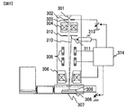
- FIG. 3 is a schematic configuration diagram of a scanning electron microscope.
- An electron beam 303 extracted from the electron source 301 by the extraction electrode 302 and accelerated by an accelerating electrode (not shown) is squeezed by a condenser lens 304 which is a form of a focusing lens, and then is scanned by a scanning deflector 305.
- 309 is scanned one-dimensionally or two-dimensionally.
- the electron beam 303 is decelerated by a negative voltage applied to an electrode built in the sample stage 308 and is focused by the lens action of the objective lens 306 and irradiated onto the sample 309.
- secondary electrons and electrons 310 such as backscattered electrons are emitted from the irradiated portion.
- the emitted electrons 310 are accelerated in the direction of the electron source by the acceleration action based on the negative voltage applied to the sample, and collide with the conversion electrode 312 to generate secondary electrons 311.
- the secondary electrons 311 emitted from the conversion electrode 312 are captured by the detector 313, and the output of the detector 313 changes depending on the amount of captured secondary electrons.
- the brightness of the display device changes according to this output.
- an image of the scanning region is formed by synchronizing the deflection signal to the scanning deflector 305 and the output of the detector 313.
- the scanning electron microscope illustrated in FIG. 8 includes a deflector (not shown) that moves the scanning region of the electron beam.
- This deflector is used to form images of patterns having the same shape existing at different positions.
- This deflector is also referred to as an image shift deflector, and enables movement of the field of view (Field of View: FOV) of the electron microscope without moving the sample by the sample stage.
- the image shift deflector and the scanning deflector may be a common deflector, and the image shift signal and the scanning signal may be superimposed and supplied to the deflector.
- the control device 314 controls each component of the scanning electron microscope, and forms a pattern based on the detected electrons and a pattern formed on the sample based on the detected electron intensity distribution called a line profile. -It has a function to measure the size of the screen.
- a storage unit 407 is provided.
- the pattern information setting unit 402 can set the number of periodic array patterns to be measured, the array, the size of the region selection pattern, and the like based on input or preset conditions.
- the template setting unit 403 creates a template by cutting out a part of an image obtained by a scanning electron microscope, design data, and a part of a pattern image obtained from an exposure simulator.
- the template created by the template setting unit 403 is stored in the template storage unit 406 or the recipe storage unit.
- the pattern arrangement and size calculation unit 404 performs pattern matching based on the templates created by the pattern information setting unit 402 and the template setting unit 403, and calculates the pattern arrangement and the pattern size.
- the overlay calculator 405 calculates the overlay based on the result of the pattern array and size calculator 404. At this time, it is also possible to consider the difference between the number of patterns, the size of the end of the region, and the size inside the region as the calculation.
- the image processor 401 may be integrated with the SEM control device, or may be an image processor separate from the SEM connected to the SEM via a network.
- FIG. 5 shows a flowchart for overlay measurement.
- the number of patterns selected in the first step is confirmed (S1), and it is determined whether or not the pattern matches the pattern registered in the recipe.
- This number can also be set in advance as a measurement condition.
- the number of the patterns 501 when the overlay error is 0 is 4, and when the overlay error is large (502), the number of lines is increased by 1 to 5 lines. If it is determined that the number is measurable, the dimensions (WL, WR) at both ends of the periodic array pattern are measured (S2). The overlap is calculated from the comparison of WL and WR and the pattern information registered in the recipe (S3).
- FIG. 12 is a flowchart for explaining in more detail the process of measuring the overlay error
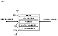
- FIG. 13 is a diagram for explaining the specific configuration of the arithmetic unit for measuring the overlay error.
- a semiconductor device semiconductor wafer
- the recipe control program for controlling the scanning electron microscope
- the object to be measured is controlled by controlling the sample stage 308 and the deflector that deflects the irradiation position of the electron beam.
- the field of view Field of View: FOV
- FOV Field of View
- an image (SEM image) of the measurement target pattern is acquired based on a signal obtained by scanning the measurement target pattern with an electron beam (step 1203).
- the pattern number counting unit 1302 measures the number of periodic array patterns (step 1302). The number of patterns is measured, for example, by obtaining a luminance profile for a predetermined area and counting the number of peaks exceeding a predetermined threshold, thereby counting the number of patterns, or pixels having a predetermined luminance appearing by binarization processing Various methods such as a method of counting the number of aggregates can be applied.
- the process proceeds to the next step without measuring the overlay error.
- a predetermined number of patterns are selected, when overlay error is measured, the relative position with other reference patterns is measured, and compared with the reference value, An alignment error measurement may be performed.
- the measurement result of the number of patterns in the predetermined area is the predetermined number n + 1 (5 in the example of FIG. 1, that is, other than the specified number)
- the dimension measuring unit 1303 is positioned at one end in the arrangement direction of the periodic arrangement pattern.
- the dimension measurement of the pattern to be performed and the pattern located at the other end is executed (step 1205).
- the SEM image acquired in step 1203 may be used, or based on the detection signal obtained by positioning the field of view on each of the one end pattern and the other end pattern.
- the pattern dimension may be measured. In order to obtain a more accurate dimensional value, it is desirable to select the latter that allows measurement at a high magnification.
- the dimension measuring unit 1303 executes pattern dimension measurement based on the distance between peaks or the peak width of the luminance profile of the pattern to be measured, and the visual field size information.
- the deviation direction / deviation amount calculation unit 1304 specifies the deviation direction based on the comparison between the pattern on the one end side and the pattern on the other end side, and calculates the deviation amount using Equation 1, Equation 2, and the like. Calculate (step 1206).
- the deviation direction / deviation amount calculation unit 1304 determines whether to obtain the overlay error using Expression 1 or to obtain the overlay error using Expression 2, depending on the direction of deviation (result of the difference calculation). . If the measurement result of the number of patterns in step 1204 is other than n, n + 1, or the count itself cannot be performed, there is a possibility that a pattern defect other than the overlay error has occurred, or that the electron microscope image is appropriate. Since it may not be formed, the pattern number counting unit 1302 outputs error information (step 1207).
- the process returns to step 1202. If there is no other measurement target pattern, the pattern number counting unit 1302 and the shift direction / shift amount calculation unit.
- the measurement result or calculation result obtained by 1304 is output to an output medium such as a display device or stored in a storage medium or the like (step 1208).
- the deviation distribution information calculation unit 1305 may calculate an index value indicating a tendency of deviation. For example, if the misalignment direction and amount are almost the same at multiple overlay error measurement positions, it is considered that overlay misalignment in a specific direction has occurred, but the misalignment direction and amount are not uniform.
- the region selection pattern or the semiconductor wafer may be deformed. Further, there is a possibility that a rotational deviation has occurred between the region selection pattern and the periodic arrangement pattern.
- a discrete deviation such as a simple overlay deviation, a rotational deviation, or a pattern deformation.
- the region selection pattern edge for selecting the region of the periodic arrangement pattern is arranged in the middle of the selection region and the non-selection region.
- the region selection pattern 604 A case where the ends are arranged at the pattern center of the periodic arrangement pattern 601 will be described.
- the dimension of the line pattern 601 is set to W and the pitch of the periodic arrangement is set to twice W as in the first embodiment.
- Reference numeral 603 denotes a relative position of the periodic arrangement pattern layer to the region selection pattern layer 602.
- the misalignment with the region selection pattern layer 602 is zero, and the shape of both ends of the selected periodic array pattern indicated by 606 and 607 is half the size of the pattern inside the region. . Therefore, the line widths at both ends are the same. In this example, five lines are formed, and a part of the pattern at both ends of the periodic array pattern is missing.
- the lower diagram in FIG. 6 is an example in the case where a deviation of the overlay between the periodic arrangement pattern 608 and the region selection pattern 609 occurs.
- Reference numeral 610 denotes a relative position of the periodic arrangement pattern with respect to the region selection pattern 609.
- the misalignment between the region selection pattern layer 609 and the periodic arrangement pattern layer 610 is caused by the pattern size WL of the patterns 612 and 613 at the left and right ends of the pattern layer 611 formed by the process of superimposing 608 and 609. , WR, and is calculated by Equation 3.
- the overlay deviation is smaller than ⁇ W.
- Overlay deviation (WR-WL) / 2 Equation 3
- the overlay size is W / 2 to W.
- Example 3 describes an example of applying a periodic array pattern formed by DSA.
- FIG. 7 is a diagram illustrating a sample state in which a region selection pattern (upper layer) for selecting a part thereof is superimposed on a plurality of patterns (lower layer) generated by a patterning method using a self-guided organization phenomenon. It is.
- the DSA line pattern forms a guide pattern (701) having different chemical properties formed by lithography in the lower layer region 702.
- a periodic array pattern (703) by DSA is generated.
- the DSA pattern period is 1/3 of the period of the lower layer guide pattern, and two lines (705) are arranged at equal intervals between the lines (704) formed on the lower layer guide line.
- the relative position or size of the DSA pattern varies depending on the relative position on the guide or from the guide. Therefore, the dimensional difference between both ends of the pattern formed by the periodic array pattern and the region selection pattern is greatly affected by the variation.
- the area selection pattern (706) can be improved in accuracy by making it the same size or an integer multiple of the periodic arrangement of the guides. In this example, 706 has the same size as the periodic arrangement of the lower layer guide patterns.
- Example 4 describes an example of applying a periodic array pattern formed by SAQP.
- FIG. 8 is a diagram showing a sample state in a state where a region selection pattern (upper layer) for selecting a part thereof is superimposed on a plurality of patterns (lower layer) generated by SAQP.
- the SAQP line pattern first forms a dummy pattern (801) formed by lithography.
- the arrangement period of the periodic arrangement pattern (802, 803, 804, 805) by SAQP is 1/4 of the period of the dummy pattern.
- the relative position of the line or its size differs for each relative arrangement from the dummy pattern.
- the area selecting pattern (806) can be improved in accuracy by making it the same size or an integer multiple of the dummy pattern periodic array.
- 806 is the same size as the periodic pattern of dummy patterns.
- FIG. 9 is a diagram illustrating a sample state in which a region selection pattern (upper layer) for selecting a part thereof is superimposed on a periodically arranged hole pattern (lower layer).
- the hole pattern of the periodic array is generated not only by DSA but also by making the periodic array pattern of SAMP orthogonal.
- the region selection pattern (902, 903) is used for the periodically arranged hole pattern (901).
- the area selection pattern 902 is an example in which holes on the left and right ends of the pattern area are not missing
- the area pattern 903 is an example in which holes on the left and right edges of the pattern area are missing. This is similar to the example of the line pattern of the first and second embodiments.
- the left and right sides are missing depending on the overlap of the hole pattern (901) of the periodic arrangement and the region selection pattern (902, 903).
- the overlapping of the size WL and WR of the end hole pattern (904, 905) is calculated.
- the example in which the region selection pattern edge for selecting the region of the periodic arrangement pattern is arranged in the middle of the selected region and the non-selected region or at the pattern center is shown.
- the width of the working pattern is an integral multiple of the pitch size of the periodic array pattern.
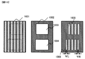
- the width of the region selection patterns 1003 and 1004 is set to be about 1 ⁇ 2 of the pattern width larger than the integral multiple of the width of the periodic array pattern 1001.
- the dimension of the periodic array line pattern 1001 is W and the pitch of the periodic array is twice W as in the first embodiment.
- the misalignment with the region selection pattern layer 1002 is 0, and the shape of the both ends of the selected periodic array pattern indicated by 1005 is the same as the inside of the region, and is indicated by 1006
- the shape of both ends of the selected periodic array pattern is about 3/4 of the size of the pattern inside the region. Therefore, the line widths at both ends are the same.
- the range of misalignment that can be measured is reduced, but the same calculation method is used for overlapping. The sum can be calculated.
- the width of both end portions 1006 of the selected periodic array pattern is thicker than the line width of the second embodiment, so that the margin for the collapse of the formed pattern is improved and the measurement accuracy is improved.
Landscapes
- Physics & Mathematics (AREA)
- Chemical & Material Sciences (AREA)
- Analytical Chemistry (AREA)
- Electromagnetism (AREA)
- General Physics & Mathematics (AREA)
- Length-Measuring Devices Using Wave Or Particle Radiation (AREA)
Abstract
本発明は、領域選択用パターンと、当該領域選択用パターンに選択される被選択パターンとの重ね合わせ評価を行うパターン計測装置の提供を目的とする。本発明は、重ね合わせ誤差を求めるパターン計測装置であって、複数のパターンが配列された試料に対する荷電粒子ビームの走査に基づいて得られた信号から、前記複数のパターンの一端に位置する第1のパターンの第1の測定値と、前記複数のパターンの他端に位置する第2のパターンの第2の測定値を求め、当該第1の測定値と第2の測定値の比較に基づいて、前記第1の層と第2の層との間の重ね合わせずれの方向、及びそのずれ量の少なくとも一方を求めるパターン計測装置を提案する。
Description
本発明は、パターン計測装置及びコンピュータープログラムに係り、特に周期配列パターンと、当該周期配列パターンの一部を選択する領域選択用パターンとの重ね合わせを評価するパターン計測装置及びコンピュータープログラムに関する。
半導体デバイスの高集積化のために、パターンの多層構造化が進んでいる。このような多層構造の半導体デバイスを生成するためには、複数のレイヤに形成された微細パターンを適正に重ね合わせる必要がある。レイヤ間(製造工程間)の重ね合わせ評価を行うために、走査電子顕微鏡(Scanning Electron Microscope:SEM)が用いられている。特許文献1には、SEMによって取得された重ね合わせ評価パターンの画像と、レイアウトデータ(理想的な状態で複数層のパターンが重ね合わせられたパターンデータ)とを比較し、重ね合わせ状態の評価を行う測定装置が説明されている。
一方、投影露光装置によって形成されるパターンをn倍化する手法の適用が検討されている。
その例として、自己誘導組織化現象を利用したパターニング法(Directed Self Assembly:DSA)がある。この方法は、高分子ブロック共重合体と言われる2種類のポリマーを合成しブロック結合させた材料を用い、2種類のポリマーの熱力学的特性の違いによって、自己組織化する現象を利用したパターニング法である。リソグラフィ技術で形成したパターン(ガイドパターン)を用いてその1/Nのピッチの複数本のパターンを自己整合的に形成することができる。
別の例としてSAMP(Self Aligned Multiple Patterning)と呼ばれる方法もある。リソグラフィ技術によって形成されたパターン(ダミーパターン)の上にCVD でSiO2 などの膜を付けエッチングすると、ダミーパターンの側壁部分のCVD膜のみが残りダミーパターンを取り除くと、ダミーパターン1/2ピッチのパターンが形成される。これを繰り返すことによりダミーパターンの1/4ピッチ、1/8ピッチのパターンを形成される。1/2ピッチ、1/4ピッチにする方法をそれぞれ、SADP(Self Aligned Double Patterning)、SAQP(Self Aligned Quadruple Patterning)と呼ぶ。これらの技術をまとめてSAMPと呼ぶ。
DSA、SAMP等により形成されるパターンは広範囲に周期的配列パターンとなる。この周期的配列パターンの一部をデバイスパターンに適用するため、適用する領域を選択するために形成するパターン(これを領域選択用パターン呼ぶこともある)を周期的配列パターンプロセスの前または後に追加する。この2つのパターンを重ね合わせることで、デバイスパターン適用する周期的配列パターンを形成する。DSA、SAMP等により形成される周期的配列パターンと領域選択用パターンとの重ね合わせの精度はデバイスの性能、歩留まりに大きく影響するためその計測が重要になると予想される。
SEM等の荷電粒子線装置を用いて、周期的配列パターンと、その所定領域のみを選択するために形成された領域選択用パターンの重ね合わせ計測を行うとき、例えば領域選択用パターンの開口部分に位置する周期的配列パターンは、SEM画像上に表示されるものの、それ以外の部分の周期的配列パターンは、領域選択用パターンに遮蔽されているため、或いは実際にパターンが選択された後では、SEM画像で確認することが困難である。即ち、周期的配列パターンと領域選択用パターンとの間の重ね合わせ状態は、領域選択用パターンの開口部分に見えている周期的配列パターンの画像、或いは実際に選択された周期配列パターンの画像から判断する必要がある。選択された周期的配列パターンは、重ね合わせの状態によって、パターンの数や端部に位置するパターンの寸法や形状が変化することになるが、特許文献1には、そのような条件下でパターン間の重ね合わせを評価する手法について、何等論じられていない。
以下に、領域選択用パターンと、当該領域選択用パターンに選択される被選択パターンとの重ね合わせ評価を目的とするパターン計測装置及びコンピュータープログラムを提案する。
上記目的を達成するための一態様として、荷電粒子線装置にて得られた信号に基づいて、第1の層に形成されたパターンと、第2の層に形成されたパターンの重ね合わせ誤差を求める演算装置を備えたパターン計測装置、或いは重ね合わせ誤差をコンピューターに演算させるコンピュータープログラムであって、前記演算装置は複数のパターンが配列された試料に対する荷電粒子ビームの走査に基づいて得られた信号から、前記複数のパターンの一端に位置する第1のパターンの第1の測定値と、前記複数のパターンの他端に位置する第2のパターンの第2の測定値を求め、当該第1の測定値と第2の測定値の比較に基づいて、前記第1の層と第2の層との間の重ね合わせずれの方向、及びそのずれ量の少なくとも一方を求めるパターン計測装置、或いはコンピュータープログラムを提案する。
また、上記目的を達成するための他の態様として、荷電粒子線装置にて得られた信号に基づいて、第1の層に形成されたパターンと、第2の層に形成されたパターンの重ね合わせ誤差を求める演算装置を備えたパターン計測装置であって、前記演算装置は、複数のパターンが配列された試料に対する荷電粒子ビームの走査に基づいて得られた信号から、前記複数のパターンの数を計数し、当該パターンの数が所定数と異なる場合に、前記複数のパターンの測定に基づいて、前記第1の層と第2の層との間の重ね合わせずれの方向、及びそのずれ量の少なくとも一方を求めるパターン計測装置を提案する。
上記構成によれば、領域選択用パターンと、当該領域選択用パターンに選択される被選択パターンとの間の重ね合わせ評価を行うことが可能となる。
以下に説明する実施例では、例えば、荷電粒子ビームの走査によって得られる取得画像を用いて、画像内の周期配列されたパターンと、その所定領域のみを選択する領域選択用パターンとの重ね合わせにより形成されたパターンにおいて、一端側の第1のパターンの測定値とパターンの他端側に配置された第2のパターンの測定値の差分演算及び比較に基づいて所定領域をパターンと前記周期配列パターンが生成された層間の測定に用いる演算式を選択する画像処理装置、或いは荷電粒子線装置について説明する。
以下に説明する実施例によれば、例えば、周期配列されたパターンと、その領域選択用パターンとの層間の重ね合わせを計測できる。
以下に説明する実施例は、走査電子顕微鏡等によって得られた所定領域のみ選択された配列パターンの端部の画像を用いて評価する方法、装置、及びコンピュータープログラムに関する。特に、周期配列されたパターンとその一部を加工パターンとして適用する領域を選択するための領域選択用パターンとの重ね合わせ測定評価が可能な方法、装置及びコンピュータープログラムに関する。
半導体素子や薄膜磁気ヘッドなど、表面の微細加工により製作される機能素子製品の製
造・検査工程では、加工されたパターン幅の測定(以下「測長」と呼ぶ)および外観検査
等に、SEMが広く用いられている。
造・検査工程では、加工されたパターン幅の測定(以下「測長」と呼ぶ)および外観検査
等に、SEMが広く用いられている。
走査電子顕微鏡は、電子源から放出され、磁場あるいは電場と電子線の相互作用を利用した収束レンズおよび対物レンズにより細く絞られた電子線を、偏向器を用いて試料上で一次元あるいは二次元的に走査し、電子線照射によって試料から発生する二次信号(二次電子や反射電子、電磁波)を、光電効果等を利用した検出器により検出し、その検出信号を電子線の走査と同期した輝度信号等の可視化可能な信号に変換・処理することで試料像を形成する装置である。
半導体素子や薄膜磁気ヘッドなど、表面の微細加工の方法としては、光リソグラフィやナノインプリントといった微細構造を光・電子線・原版等によりパターンを形成する方法が一般に用いられている。
周期的配列パターン形成方法の例として、ここでは3つの方法を紹介する。まず一つ目は自己組織化現象を利用して微細な規則構造を形成するDSAがある。この例としては、ポリスチレン(PS)とポリメチルメタクリレート(PMMA)からなる高分子ブロック共重合体薄膜を用いて、規則配列された孔やラインアンドスペースのパターンを基板上に形成した公知技術が知られている。この際、形成される周期パターンの形状(孔またはラインアンドスペース等)、その形状の周期的配列のピッチ等は、高分子ブロック共重合体組成物を含む高分子層の各分子量・混合比等で決まる。
自己組織化により形成するパターン配列を所望の範囲とし、その範囲の配列を揃えるため、2つの方法が考案されている。
自己組織化による第1の方法は、下地基板表面に溝・孔を加工し、それをガイドとしてその内部に高分子ブロック共重合体組成物を含む高分子層を成膜して規則配列パターンを形成させる方法である。ガイドは配列が安定するように自己組織化のパターン周期の2倍から十倍程度となるような大きさとする。微細構造はガイドによって制限された範囲で配列し、自己組織化の長距離秩序性が向上する。
自己組織化による第1の方法は、下地基板表面に溝・孔を加工し、それをガイドとしてその内部に高分子ブロック共重合体組成物を含む高分子層を成膜して規則配列パターンを形成させる方法である。ガイドは配列が安定するように自己組織化のパターン周期の2倍から十倍程度となるような大きさとする。微細構造はガイドによって制限された範囲で配列し、自己組織化の長距離秩序性が向上する。
自己組織化による第2の方法は、下地基板表面を化学的にパターン化する方法である。基板表面には高分子ブロック共重合体を構成する各々のブロック鎖に対して親和性が異なる領域をパターンとして形成する。たとえばポリスチレンとポリメチルメタクリレートからなる高分子ブロック共重合において、ポリスチレンと化学的に親和性の良い領域を、自己組織化の周期の約半分の大きさで、自己組織化の周期の2倍から十倍程度の周期で配列する。それ以外領域をポリスチレンとポリメチルメタクリレートと同じ親和性を持つように化学的に形成する。この基板表面上の高分子ブロック共重合体の自己組織化によるパターンは、ポリスチレンと化学的に親和性の良い領域をガイドとして、ガイド上にポリスチレンが形成され、それ以外の領域はガイド上のポリスチレンパターンからの周期的配列となり、自己組織化の長距離秩序性が向上する。
二つ目の周期的配列パターン形成方法の例としては、SAMP(Self Align Multiple Patterning)と呼ばれる方法がある。リソグラフィ技術によって形成されたパターン(ダミーパターン)の上にCVD でSiO2 などの膜を付けエッチング等の工程を行い、ダミーパターン1/2ピッチのパターンが形成される。このパターンにおいてはパターンのレイアウトがダミーパターンの配置に限定される。ダミーパターンは周期的配列で形成される場合が多く、そのためパターンの一部を削除または選択するプロセスが必要となる。
三つ目の周期的配列パターン形成方法の例として、ある周期の配列に特化した証明条件でリソグラフィを行う方法がある。さらにDouble Patterning(以下DP)とよばれる複数回の露光を組み合わせて周期的配列パターンを形成する。このパターンは周期的配列に特化したリソグラフィ技術で形成されるため、パターンの一部を削除または選択するプロセスが必要となる。
このDSA、SAMP、DPによる周期的配列パターンは 形成するパターン配列を揃えて生成する、前記ガイドまた、下地基板表面の科学的パターン及びダミーパターンは一般にリソグラフィ技術によって生成され、そのパターンはその下層パターンとの重ね合わせを計測、調整して形成される。また形成される周期的配列パターンは、リソグラフィ以降のプロセスに起因してその配列からのずれ及びその寸法が変動する。
この周期的配列パターンの一部をデバイスパターンに適用するため、適用する領域を選択し、デバイスパターンとするための領域選択用パターンを形成するプロセスを適用する。 この2つのパターンを重ね合わせることで、デバイスパターン適用する周期的配列パターンを形成する。
以下に説明する実施例では、主に上記のような周期的配列パターンと領域選択用パターンにより形成されるパターンについて、その重ね合わせ等のプロセス評価する画像処理の方法や装置に関するものである。このような画像処理によってもたらされる測定結果は、周期的配列パターンと領域選択用パターンとの重ね合わせ評価、領域選択用パターンによる周期的配列の選択領域形成技術の評価に用いられる。
以下に説明する実施例では、この相対位置の重ね合わせずれを計測する方法及び評価する画像処理の方法を提案する。また、画像を形成する装置として荷電粒子線装置を例示すると共に、その一態様として、SEMを用いた例を説明するが、これに限られることはなく、例えば試料上にイオンビ-ムを走査して画像を形成する集束イオンビ-ム(Focused Ion Beam:FIB)装置を荷電粒子線装置として採用するようにしても良い。また、撮像された画像の視野内に領域が選択された周期配列パターンを画像処理に基づいて評価することができるのであれば、撮像装置の種類は問わない。
図1は本実施例における測定法の原理を説明する図である。101はDSAまたはSAMP等で形成された周期的配列パターンである。102は101のうちデバイスパターンとする領域を選択する領域選択用パターンであり、105は101及び102を重ね合わせたプロセスにより形成されるパターンである。102で選択された領域の周期的配列パターンのみが105におけるパターンとなる。一般に領域選択用パターンの端は選択する領域と選択しない領域の中間に配置する。103は周期的配列パターン層の領域選択用パターン層102に対する相対位置を示している。この場合、領域選択用パターン層102との重ね合わせのずれは0であり、106、107で示された選択された周期的配列パターンの両端部の形状は領域内部のパターンの形状と同じである。したがってその両端部の線幅は同じになる。この例では4本の周期的配列ラインが形成される。
なお、図1と同等の図を図11にも例示する。図11の例では理解が容易なように、領域用選択パターンの開口の輪郭1101のみが選択的に表記されている。輪郭1101は、被選択パターンである周期的配列パターン1102に、領域選択用パターンが適切に重ね合わせられた状態における領域選択パターンの開口を示している。
図1の下の図は周期的配列パターン108と領域選択用パターン109の重ね合わせのずれが発生した場合の例である。110は周期的配列パターンの領域選択用パターン109に対する相対位置を示している。この例では重ね合わせのずれにより、所望のライン4本よりも1本多い5本が形成されている。図11では輪郭1103が図1の下図と同じ状態を示している。
本実施例では、所定値以上の重ね合わせ誤差がある場合、領域選択用パターンにて選択される被選択パターンが、所定数より多く存在する現象を利用して、重ね合わせ誤差の測定を行う。図1の下図の例では、左側端部(一旦側)に位置するパターン線幅111、右側端部(他端側)に位置するパターン線幅112の比較(差分演算)から周期的配列パターンの領域選択用パターンの重ね合わせ誤差を算出することができる。
101のラインパターンの寸法をW(パターンの本来の寸法)、周期的配列のピッチをWの2倍(2W)とし、重ね合わせずれが0のときの、領域選択パターンにより選択される領域の境界がラインパターンの中間にとなるプロセスを想定する。重ねあわせのずれにより、がライン5本が形成(選択)される場合、左右端のパターン111、112の線幅をそれぞれWL、WRとするとそれらを用いて重ね合わせは下記式によって算出される。この場合合わせずれは±Wよりも小さいことを前提とする。
WL>WRのときは、重ねあわせずれ=(WR-WL)/2+W(式1)、WL<WRのときは、重ねあわせずれ=(WR-WL)/2-W(式2)で重ね合わせ誤差dを求めることができる。
またラインが4本の場合は重ねあわせが±W/2以下であることを示している。この重ね合わせのずれは製造プロセスの変動により発生するため、プロセスを安定させるためには、上述のような計測法を採用すると共に、計測結果を適正にプロセスにフィードバックする必要がある。実施例では矩形の領域選択用パターンを用いて周期的配列のライン4本を選択する例を示したが、領域選択用パターンの形状および選択されるパターンの数は任意に変更できる。また、この例では周期的配列のピッチをラインパターン寸法Wの2倍としたが、それ以外のピッチにおいても同様な方法で重ねあわせを算出できる。
また、この例では縦方向の周期的配列のラインパターンを用いてX方向の重ね合わせを計測したが、横方向の周期的配列のラインパターンを用いることでY方向の重ね合わせを計測することもできる。
なお、本実施例では重ね合わせずれが、Wより小さい前提でWL>WRのときには、所望の位置より右側(正側)に領域選択用パターンが位置する(例えば輪郭1103)ことが判り、WL<WRのときには、所望の位置より左側(負側)に領域選択用パターンが位置する(例えば輪郭1104)ことがわかる。よって、ずれの方向情報を、上記ずれ量に代えて、或いはずれ量とずれの方向情報を併せてデータ化することができる。以下に、そのような演算や出力を行う演算装置を含む測定、検査システムについて説明する。
図2は、複数の測定、或いは検査装置がネットワ-クに接続された測定、検査システムの概略説明図である。当該システムには、主に半導体ウェハやフォトマスク等のパタ-ン寸法を測定、あるいは検査するSEM201、202、203がネットワ-クに接続された構成となっている。また、ネットワ-クには、半導体デバイスの設計デ-タ上で、測定位置や測定条件等を設定し、且つ得られたSEM画像に基づいて、測定や検査を行う画像処理装置、或いはパターン計測装置としても機能する条件設定装置204、半導体デバイスの設計デ-タと、半導体製造装置の製造条件等に基づいて、パタ-ンの出来栄えをシミュレ-ションするシミュレ-タ-205、及び半導体デバイスのレイアウトデ-タや製造条件が登録された設計デ-タが記憶される記憶媒体206が接続されている。
設計デ-タは例えばGDSフォ-マットやOASISフォ-マットなどで表現されており、所定の形式にて記憶されている。なお、設計デ-タは、設計デ-タを表示するソフトウェアがそのフォ-マット形式を表示でき、図形デ-タとして取り扱うことができれば、その種類は問わない。また、記憶媒体206は測定装置、検査装置の制御装置、或いは条件設定装置204、シミュレ-タ-205に内蔵するようにしても良い。なお、シミュレ-タ-205は、設計デ-タに基づいて、欠陥発生位置をシミュレ-ションする機能を備えている。
なお、SEM201、202、203には、それぞれの制御装置が備えられ、各装置に必要な制御が行われるが、これらの制御装置に、上記シミュレ-タ-の機能や測定条件等の設定機能を搭載するようにしても良い。
SEMでは、電子源より放出される電子ビ-ムが複数段のレンズにて集束されると共に、集束された電子ビ-ムは走査偏向器によって、試料上を一次元的、或いは二次元的に走査される。
電子ビ-ムの走査によって試料より放出される二次電子(Secondary Electron: SE)或いは後方散乱電子(Back scattered Electron:BSE)は、検出器により検出され、前記走査偏向器の走査に同期して、フレ-メモリ等の記憶媒体に記憶される。このフレ-ムメモリに記憶されている画像信号は、制御装置内に搭載された演算装置によって積算される。また、走査偏向器による走査は任意の大きさ、位置、及び方向について可能である。
以上のような制御等は、各SEMの制御装置にて行われ、電子ビ-ムの走査の結果、得られた画像や信号は、通信回線ネットワ-クを介して条件設定装置204に送られる。なお、本例では、SEMを制御する制御装置と、条件設定装置204を別体のものとして、説明しているが、これに限られることはなく、条件設定装置204にて装置の制御と測定処理を一括して行うようにしても良いし、各制御装置にて、SEMの制御と測定処理を併せて行うようにしても良い。
また、上記条件設定装置204或いは制御装置には、測定処理を実行するためのプログラムが記憶されており、当該プログラムに従って測定、或いは演算が行われる。
また、条件設定装置204は、SEMの動作を制御するプログラム(レシピ)を、半導体の設計デ-タに基づいて作成する機能が備えられており、レシピ設定部として機能する。具体的には、設計デ-タ、パタ-ンの輪郭線デ-タ、或いはシミュレ-ションが施された設計デ-タ上で所望の測定点、オートフォーカス、オ-トスティグマ、アドレッシング点等のSEMにとって必要な処理を行うための位置等を設定し、当該設定に基づいて、SEMの試料ステ-ジや偏向器等を自動制御するためのプログラムを作成する。
図3は、走査電子顕微鏡の概略構成図である。電子源301から引出電極302によって引き出され、図示しない加速電極によって加速された電子ビ-ム303は、集束レンズの一形態であるコンデンサレンズ304によって、絞られた後に、走査偏向器305により、試料309上を一次元的、或いは二次元的に走査される。電子ビ-ム303は試料台308に内蔵された電極に印加された負電圧により減速されると共に、対物レンズ306のレンズ作用によって集束されて試料309上に照射される。
電子ビ-ム303が試料309に照射されると、当該照射個所から二次電子、及び後方散乱電子のような電子310が放出される。放出された電子310は、試料に印加される負電圧に基づく加速作用によって、電子源方向に加速され、変換電極312に衝突し、二次電子311を生じさせる。変換電極312から放出された二次電子311は、検出器313によって捕捉され、捕捉された二次電子量によって、検出器313の出力が変化する。
この出力に応じて図示しない表示装置の輝度が変化する。例えば二次元像を形成する場合には、走査偏向器305への偏向信号と、検出器313の出力との同期をとることで、走査領域の画像を形成する。また、図8に例示する走査電子顕微鏡には、電子ビ-ムの走査領域を移動する偏向器(図示せず)が備えられている。この偏向器は異なる位置に存在する同一形状のパタ-ンの画像等を形成するために用いられる。この偏向器はイメ-ジシフト偏向器とも呼ばれ、試料ステ-ジによる試料移動等を行うことなく、電子顕微鏡の視野(Field Of View:FOV)位置の移動を可能とする。イメ-ジシフト偏向器と走査偏向器を共通の偏向器とし、イメ-ジシフト用の信号と走査用の信号を重畳して、偏向器に供給するようにしても良い。
なお、図3の例では試料から放出された電子を変換電極にて一端変換して検出する例について説明しているが、無論このような構成に限られることはなく、例えば加速された電子の軌道上に、電子倍像管や検出器の検出面を配置するような構成とすることも可能である。
制御装置314は、走査電子顕微鏡の各構成を制御すると共に、検出された電子に基づいて画像を形成する機能や、ラインプロファイルと呼ばれる検出電子の強度分布に基づいて、試料上に形成されたパタ-ンのサイズを測定する機能を備えている。
図4に例示する画像処理プロセッサ401(演算装置)は、パターン情報設定部402、テンプレート設定部403、パターン配列およびサイズ演算部404、重ね合わせ演算部405、パターン配列およびテンプレート記憶部406、計測結果記憶部407を備えている。
パターン情報設定部402では、入力或いは予め設定された条件に基づいて、計測する周期的配列パターンの数、配列、領域選択用パターンのサイズ等を設定することも可能である。テンプレート設定部403では走査電子顕微鏡によって得られた画像の一部、デザインデータ、露光シミュレーターから得られるパターン像の一部を切り出してテンプレートを作成する。テンプレート設定部403にて作成されるテンプレートはテンプレート記憶部406あるいはレシピ記憶部に記憶される。
パターン配列およびサイズ演算部404では、パターン情報設定部402およびテンプレート設定部403にて作成されたテンプレートに基づいて、パターンマッチングを実行し、パターン配列およびパターンサイズの演算を行う。重ね合わせ演算部405ではパターン配列およびサイズ演算部404の結果を元に重ねあわせを算出する。この際、パターンの数、領域端部のサイズと領域内部のサイズとの差を演算として考慮することも可能である。
なお、画像処理プロセッサ401は、SEMの制御装置と一体としても良いし、SEMとネットワーク経由で接続されるSEMとは別体の画像処理装置とするようにしても良い。
図5は重ね合わせ計測におけるフローチャートを示している。画像を取得後、始めにで選択されたパターンの本数を確認し(S1)、レシピに登録されたパターンと一致するか判断する。この本数は計測条件としてあらかじめ設定することも可能である。実施例1の計測パターンでは、重ね合わせずれ0のときのパターン501の本数は4本であり、重ね合わせずれが大きい場合(502)はライン本数1本多い5本となる。計測可能な本数と判断したらその周期的配列パターンの両端の寸法(WL、WR)を計測する(S2)。そのWL,WRの比較、レシピに登録されたパターン情報から重ねあわせを算出する(S3)。
図12は、重ね合わせ誤差計測を行う工程をより詳細に説明するフローチャートであり、図13は、重ね合わせ誤差計測を行う演算装置の具体的な構成を説明する図である。まず、図3に例示するような走査電子顕微鏡に半導体デバイス(半導体ウェハ)を導入する(ステップ1201)。次にレシピ記憶部等に記憶されたレシピ(走査電子顕微鏡を制御するための制御プログラム)情報に基づいて、試料台308や電子ビームの照射位置を偏向する偏向器を制御することによって、測定対象となるパターンに視野(Field Of View:FOV)を位置付ける(ステップ1202)。領域選択用パターンによって選択される領域の座標情報を、予めレシピに登録しておくことによって、上記のような制御が可能となる。
次に、測定対象パターンに電子ビームを走査することによって得られる信号に基づいて、測定対象パターンの画像(SEM画像)を取得する(ステップ1203)。パターン計測装置に内蔵される演算装置1301では、パターン数計数部1302が周期的配列パターンの数を計測する(ステップ1302)。パターン数の計測は例えば、所定領域について輝度プロファイルを取得し、所定の閾値を超えたピークの数をカウントすることによって、パターンの数を計数する手法や、2値化処理によって現れる所定輝度の画素の集合体の数を計数する手法等、種々の手法の適用が可能である。
次に、所定領域のパターン数の計測結果が所定数(n本、図1の例では4本)であれば、領域選択用パターンによって、所望のパターンが選択されている状態(即ち、領域選択用パターンと周期的配列パターンとの重ね合わせ誤差がない状態)であるため、重ね合わせ誤差測定を行うことなく、次の工程に移行する。なお、所定数のパターンが選択されている状態でもなお、重ね合わせ誤差の測定を行う場合は、他の基準となるパターンとの相対位置を測定し、基準値との比較を行うことで、重ね合わせ誤差測定を行うようにしても良い。所定領域のパターン数の計測結果が、所定数n+1(図1の例では5本、即ち規定数以外)である場合には、寸法測定部1303によって、周期的配列パターンの配列方向の一端に位置するパターンと、他端に位置するパターンの寸法測定を実行する(ステップ1205)。なお、パターン寸法の測定の際には、ステップ1203にて取得したSEM画像を用いるようにしても良いし、一端のパターンと他端のパターンのそれぞれに視野を位置付けることによって得られる検出信号に基づいて、パターン寸法を測定するようにしても良い。より正確な寸法値を得るためには、高倍率での測定が可能な後者を選択することが望ましい。寸法測定部1303は、計測対象となるパターンの輝度プロファイルのピーク間の距離、或いはピーク幅等と、視野の大きさ情報に基づいて、パターン寸法測定を実行する。
次に、ずれ方向/ずれ量演算部1304では、一端側のパターンと他端側のパターンとの比較に基づいて、ずれの方向を特定すると共に、式1、式2等を用いてずれ量を算出する(ステップ1206)。ずれ方向/ずれ量演算部1304は、ずれの方向(差分演算の結果)に応じて、式1を用いて重ね合わせ誤差を求めるか、式2を用いて重ね合わせ誤差を求めるかの判定を行う。なお、ステップ1204におけるパターン数の計測結果が、n、n+1以外、或いは計数自体ができない場合には、重ね合わせ誤差とは別のパターン不良が発生している可能性や、電子顕微鏡画像が適正に形成されていない可能性があるため、パターン数計数部1302はエラー情報を出力する(ステップ1207)。
次に、レシピ情報に基づいて、他の測定対象パターンが存在する場合には、ステップ1202に戻り、他の測定対象パターンがない場合には、パターン数計数部1302やずれ方向/ずれ量演算部1304によって得られた測定結果や演算結果を、表示装置等の出力媒体に出力、或いは記憶媒体等に記憶させる(ステップ1208)。なお、1の試料について、重ね合わせ誤差測定位置が複数ある場合、ずれ分布情報算出部1305にて、ずれの傾向を示す指標値等を算出するようにしても良い。例えば複数の重ね合わせ誤差測定位置で、ずれの方向やずれ量がほぼ同じである場合には、特定方向への重ね合わせずれが発生していると考えられるが、ずれの方向や量が均一でないような場合は、領域選択用パターンや半導体ウェハが変形している可能性がある。また、領域選択用パターンと周期的配列パターンとの間に回転ずれが発生している可能性もある。表示装置にずれのベクトルの分布表示を行うことによって、単なる重ね合わせずれ、回転ずれ、パターンの変形等の離散的なずれ等の判定を行うことが可能となる。
実施例1では、周期的配列パターンの領域を選択する領域選択用パターン端を、選択する領域と選択しない領域の中間に配置した例を示したが、本実施例では、領域選択用パターン604の端を周期的配列パターン601のパターン中心に配列した場合を説明する。この例では実施例1と同様に601のラインパターンの寸法をW、周期的配列のピッチをWの2倍とする。603は周期的配列パターン層の領域選択用パターン層602に対する相対位置を示している。この場合、領域選択用パターン層602との重ね合わせのずれは0であり、606、607で示された選択された周期的配列パターンの両端部の形状は領域内部のパターンの半分のサイズである。したがってその両端部の線幅は同じになる。この例ではライン5本が形成され周期的配列パターンの両端部のパターンは一部が欠ける。
図6の下の図は周期的配列パターン608と領域選択用パターン609の重ね合わせのずれが発生した場合の例である。610は周期的配列パターンの領域選択用パターン609に対する相対位置を示している。この例では領域選択用パターン層609と周期的配列パターン層610の重ねあわせのずれは、608及び609を重ね合わせたプロセスにより形成されるパターン層611の左右端のパターン612、613のパターンサイズWL、WRを用いて、式3によって算出される。この場合重ね合わせずれは±Wよりも小さいことを前提とする。
重ねあわせずれ=(WR-WL)/2・・・式3
またラインが4本の場合は重ねあわせの大きさがW/2~Wであることを示している。実施例1のパターン配置の計測結果と組み合わせることで、重ね合わせをずれ量±Wの範囲で計測するこことができる。
またラインが4本の場合は重ねあわせの大きさがW/2~Wであることを示している。実施例1のパターン配置の計測結果と組み合わせることで、重ね合わせをずれ量±Wの範囲で計測するこことができる。
実施例3では、DSAにより形成された周期的配列パターン適用時の例を説明する。図7は、自己誘導組織化現象を利用したパターニング法によって生成された複数のパターン(下層)に、その一部を選択する領域選択用パターン(上層)を重畳させた状態の試料状況を示す図である。DSAのラインパターンは下層領域702にリソグラフィ技術で形成された化学的性質の異なるガイドパターン(701)を形成する。その上にDSAによる周期的配列パターン(703)を生成する。この例ではDSAのパターン周期は下層ガイドパターンの周期の1/3であり、下層ガイドライン上に形成されるライン(704)の間に等間隔で二本のライン(705)が配置される。ガイドの形成からDSAによるパターン形成のプロセスの条件により、DSAのパターンはガイド上、またはガイドからの相対位置に依存して、その相対位置またはそのサイズが変動する。そのため、周期的配列パターンと領域選択用パターンにより形成されるパターン両端部の寸法差は、その変動の影響を大きく受ける。これを低減するために、領域選択用パターン(706)はそのガイドの周期配列と同じサイズまたは整数倍にすることにより精度を向上することができる。この例では706は下層ガイドパターンの周期配列と同じサイズである。
実施例4では、SAQPにより形成された周期的配列パターン適用時の例を説明する。図8は、SAQPによって生成された複数のパターン(下層)に、その一部を選択する領域選択用パターン(上層)を重畳させた状態の試料状況を示す図である。SAQPのラインパターンは初めにリソグラフィ技術で形成されたダミーパターン(801)を形成する。SAQPによる周期的配列パターン(802,803,804,805)の配列周期はダミーパターンの周期の1/4である。ダミーパターン形成からSAQPによるパターン形成のプロセスの条件により、ダミーパターンからの相対配置ごとに、ラインの相対位置またはそのサイズが異なる。このため、周期的配列パターンと領域選択用パターンにより形成されるパターン両端部の寸法差は、その変動の影響を大きく受ける。これを低減するために、領域選択用パターン(806)はそのダミーパターンの周期配列と同じサイズまたは整数倍にすることにより精度を向上することができる。この例では806はダミーパターンの周期配列と同じサイズである。
実施例1では、DSA及びSAMPによる周期的配列の例としてラインパターンを形成する例を示したが、本実施例では周期的配列のホールパターンを対象とした重ね合わせ測定を行う例について説明する。図9は、周期的配列のホールパターン(下層)に、その一部を選択する領域選択パターン(上層)を重畳させた状態の試料状況を示す図である。周期的配列のホールパターンはDSAだけでなく、SAMPの周期的配列パターンを直交させて生成するなどの方法がある。
周期的配列のホールパターン(901)に対し、領域選択パターン(902,903)を用いる。領域選択パターン902は、パターン領域の左右端のホールが欠けていない例であり、領域パターン903はパターン領域の左右端のホールが欠けている例である。これは実施例1、実施例2のラインパターンの例と同様に、周期的配列のホールパターン(901)と、領域選択パターン(902,903)との重ね合わせに依存して、欠けている左右端のホールパターン(904,905)のサイズWL、WRの重ね合わせが算出される。
実施例1、2では、周期的配列パターンの領域を選択する領域選択用パターン端を、選択する領域と選択しない領域の中間に配置またはパターン中心に配置した例を示したが、いずれも領域選択用パターンの幅は周期的配列パターンのピッチサイズの整数倍となっている。
本実施例では、領域選択用パターン1003,1004の幅を周期配列パターン1001の幅の整数倍よりもパターン幅の約1/2大きくした場合を説明する。
この例では実施例1と同様に1001の周期配列ラインパターンの寸法をW、周期的配列のピッチをWの2倍とする。この場合、領域選択用パターン層1002との重ね合わせのずれは0であり、1005で示された選択された周期的配列パターンの両端部の形状は領域内部と同じであり、1006で示された選択された周期的配列パターンの両端部の形状は領域内部のパターン約3/4のサイズである。したがってその両端部の線幅は同じになる。
実施例1、2と同様に選択された周期的配列パターンの両端部の幅WL、WRから同様に算出することができるが、計測できる合わせずれの範囲が小さくなるが、同様の算出方法で重ね合わせを算出できる。
この実施例では選択された周期的配列パターンの両端部1006の幅は実施例2の線幅よりも太く、形成されるパターンの崩れに対するマージンが向上し、計測精度向上する。
ここでは領域選択用のパターンのサイズを想定して議論しているが、そのサイズはプロセス条件により変動する。安定しないプロセスでは領域選択用パターンのサイズを変更して、重ね合わせを評価し精度の高いパターンを選択することも計測精度向上に有効である。
101 周期的配列パターン
102 領域選択用パターン層
103 周期的配列パターン層
104 領域選択用パターン
105 領域選択された周期的配列パターン層
106、107 領域選択されたパターンのパターン端
201、202、203 SEM
204 条件設定装置
205 シミュレーター
206 記憶媒体
301 電子源
302 引出電極
303 電子ビーム
304 コンデンサレンズ
305 走査偏向器
306 対物レンズ
307 試料室
308 試料台
309 試料
310 電子
311 二次電子
312 変換電極
313 検出器
314 制御装置
401 画像処理プロセッサ
402 パターン情報設定部
403 テンプレート設定部
404 パターン配列およびサイズ演算部
405 重ね合わせ演算部
406 パターン配列およびテンプレート記憶部
407 演算結果記憶部
501、502 領域選択された周期的配列パターン
601 周期的配列パターン
602 領域選択用パターン層
603 周期的配列パターン層
604 領域選択用パターン
605 領域選択された周期的配列パターン層
606、607 領域選択された周期配列パターンのパターン端
608 周期的配列パターン
609 領域選択用パターン層
610 周期的配列パターン層
611 領域選択された周期的配列パターン層
612、613 領域選択されたパターンのパターン端
701 DSAの下層ガイドパターン
702 DSAの下層領域
703 DSAパターン層
704 下層ガイドパターン上DSAパターン
705 下層ガイドパターン上ではないDSAパターン
706 領域選択用パターン
701 SAQPのダミーパターン
802、803、804、805 SAQPのラインパターン、DSAの下層領域
806 領域選択用パターン
901 周期的配列ホールパターン
902、903 領域選択用パターン
904、905 領域選択された周期配列パターンのパターン端
1001 周期的配列パターン
1002 領域選択用パターン層
1003、1004 領域選択用パターン
1005、1006 領域選択された周期的配列パターン
102 領域選択用パターン層
103 周期的配列パターン層
104 領域選択用パターン
105 領域選択された周期的配列パターン層
106、107 領域選択されたパターンのパターン端
201、202、203 SEM
204 条件設定装置
205 シミュレーター
206 記憶媒体
301 電子源
302 引出電極
303 電子ビーム
304 コンデンサレンズ
305 走査偏向器
306 対物レンズ
307 試料室
308 試料台
309 試料
310 電子
311 二次電子
312 変換電極
313 検出器
314 制御装置
401 画像処理プロセッサ
402 パターン情報設定部
403 テンプレート設定部
404 パターン配列およびサイズ演算部
405 重ね合わせ演算部
406 パターン配列およびテンプレート記憶部
407 演算結果記憶部
501、502 領域選択された周期的配列パターン
601 周期的配列パターン
602 領域選択用パターン層
603 周期的配列パターン層
604 領域選択用パターン
605 領域選択された周期的配列パターン層
606、607 領域選択された周期配列パターンのパターン端
608 周期的配列パターン
609 領域選択用パターン層
610 周期的配列パターン層
611 領域選択された周期的配列パターン層
612、613 領域選択されたパターンのパターン端
701 DSAの下層ガイドパターン
702 DSAの下層領域
703 DSAパターン層
704 下層ガイドパターン上DSAパターン
705 下層ガイドパターン上ではないDSAパターン
706 領域選択用パターン
701 SAQPのダミーパターン
802、803、804、805 SAQPのラインパターン、DSAの下層領域
806 領域選択用パターン
901 周期的配列ホールパターン
902、903 領域選択用パターン
904、905 領域選択された周期配列パターンのパターン端
1001 周期的配列パターン
1002 領域選択用パターン層
1003、1004 領域選択用パターン
1005、1006 領域選択された周期的配列パターン
Claims (11)
- 荷電粒子線装置にて得られた信号に基づいて、第1の層に形成されたパターンと、第2の層に形成されたパターンの重ね合わせ誤差を求める演算装置を備えたパターン計測装置において、
前記演算装置は、複数のパターンが配列された試料に対する荷電粒子ビームの走査に基づいて得られた信号から、前記複数のパターンの一端に位置する第1のパターンの第1の測定値と、前記複数のパターンの他端に位置する第2のパターンの第2の測定値を求め、当該第1の測定値と第2の測定値の比較に基づいて、前記第1の層と第2の層との間の重ね合わせずれの方向、及びそのずれ量の少なくとも一方を求めることを特徴とするパターン計測装置。 - 請求項1において、
前記演算装置は、前記第1の測定値と第2の測定値の比較に基づいて、前記重ね合わせ誤差を求める演算式を切り替えることを特徴とするパターン計測装置。 - 請求項2において、
前記演算装置は、前記第1の測定値が前記第2の測定値より大きい場合には、((第2の測定値-第1の測定値)/2+(パターンの本来の寸法))の演算に基づいて、前記重ね合わせ誤差を求め、前記第1の測定値が前記第2の測定値より小さい場合には、((第2の測定値-第1の測定値)/2-(パターンの本来の寸法))の演算に基づいて、前記重ね合わせ誤差を求めることを特徴とするパターン計測装置。 - 請求項1において、
前記演算装置は、((第2の測定値-第1の測定値)/2)の演算に基づいて、前記重ね合わせ誤差を求めることを特徴とするパターン計測装置。 - 請求項1において、
前記複数のパターンは、周期的に配列されたパターンであることを特徴とするパターン計測装置。 - 請求項1において、
前記第1の層及び前記第2の層の一方には、前記複数のパターンの一部の領域を選択する領域選択用パターンが設けられていることを特徴とするパターン計測装置。 - 請求項1において、
前記複数のパターンは、自己組織化現象を利用したパターニング法で形成されたパターンであって、前記第1の測定値と第2の測定値は、自己組織化現象を利用したパターニング法に用いられるガイド上に形成されるパターンの測定に基づいて求められることを特徴とするパターン計測装置。 - 請求項1において、
前記複数のパターンは、マルチパターニングによって形成されたパターンであって、前記第1の測定値と第2の測定値の少なくとも一方は、マルチパターニングに用いられるダミーパターンの測定に基づいて求められることを特徴とするパターン計測装置。 - 荷電粒子線装置にて得られた信号に基づいて、第1の層に形成されたパターンと、第2の層に形成されたパターンの重ね合わせ誤差の演算をコンピューターに実行させるコンピュータープログラムにおいて、
前記プログラムは、複数のパターンが配列された試料に対する荷電粒子ビームの走査に基づいて得られた信号から、前記複数のパターンの一端に位置する第1のパターンの第1の測定値と、前記複数のパターンの他端に位置する第2のパターンの第2の測定値を求めさせ、当該第1の測定値と第2の測定値の比較に基づいて、前記第1の層と第2の層との間の重ね合わせずれの方向、及びそのずれ量の少なくとも一方を求めさせることを特徴とするコンピュータープログラム。 - 荷電粒子線装置にて得られた信号に基づいて、第1の層に形成されたパターンと、第2の層に形成されたパターンの重ね合わせ誤差を求める演算装置を備えたパターン計測装置において、
前記演算装置は、複数のパターンが配列された試料に対する荷電粒子ビームの走査に基づいて得られた信号から、前記複数のパターンの数を計数し、当該パターンの数が所定数と異なる場合に、前記複数のパターンの測定に基づいて、前記第1の層と第2の層との間の重ね合わせずれの方向、及びそのずれ量の少なくとも一方を求めることを特徴とするパターン計測装置。 - 請求項10において、
前記演算装置は、前記パターンの数が所定数と異なる場合に、前記複数のパターンの一端に位置する第1のパターンの第1の測定値と、前記複数のパターンの他端に位置する第2のパターンの第2の測定値を求め、当該第1の測定値と第2の測定値の比較に基づいて、前記第1の層と第2の層との間の重ね合わせずれの方向、及びそのずれ量の少なくとも一方を求めることを特徴とするパターン計測装置。
Priority Applications (1)
| Application Number | Priority Date | Filing Date | Title |
|---|---|---|---|
| PCT/JP2016/052561 WO2017130366A1 (ja) | 2016-01-29 | 2016-01-29 | パターン計測装置及びコンピュータープログラム |
Applications Claiming Priority (1)
| Application Number | Priority Date | Filing Date | Title |
|---|---|---|---|
| PCT/JP2016/052561 WO2017130366A1 (ja) | 2016-01-29 | 2016-01-29 | パターン計測装置及びコンピュータープログラム |
Publications (1)
| Publication Number | Publication Date |
|---|---|
| WO2017130366A1 true WO2017130366A1 (ja) | 2017-08-03 |
Family
ID=59397618
Family Applications (1)
| Application Number | Title | Priority Date | Filing Date |
|---|---|---|---|
| PCT/JP2016/052561 Ceased WO2017130366A1 (ja) | 2016-01-29 | 2016-01-29 | パターン計測装置及びコンピュータープログラム |
Country Status (1)
| Country | Link |
|---|---|
| WO (1) | WO2017130366A1 (ja) |
Cited By (1)
| Publication number | Priority date | Publication date | Assignee | Title |
|---|---|---|---|---|
| TWI723930B (zh) * | 2019-08-23 | 2021-04-01 | 日商日立全球先端科技股份有限公司 | 重疊計測系統及重疊計測裝置 |
Citations (5)
| Publication number | Priority date | Publication date | Assignee | Title |
|---|---|---|---|---|
| JPH1144664A (ja) * | 1997-07-29 | 1999-02-16 | Matsushita Electron Corp | 重ね合わせ測定方法及び測定装置及び測定パターン |
| JP2001332470A (ja) * | 2000-05-19 | 2001-11-30 | Hitachi Ltd | 半導体集積回路装置およびその製造方法 |
| US20050260510A1 (en) * | 2003-09-26 | 2005-11-24 | Heiko Hommen | Method for determining the relative positional accuracy of two structure elements on a wafer |
| JP2009115788A (ja) * | 2007-10-10 | 2009-05-28 | Asml Netherlands Bv | ダブルパターニング基板のオーバレイ測定 |
| JP2015099054A (ja) * | 2013-11-18 | 2015-05-28 | 株式会社日立ハイテクノロジーズ | オーバーレイ計測方法および計測装置 |
-
2016
- 2016-01-29 WO PCT/JP2016/052561 patent/WO2017130366A1/ja not_active Ceased
Patent Citations (5)
| Publication number | Priority date | Publication date | Assignee | Title |
|---|---|---|---|---|
| JPH1144664A (ja) * | 1997-07-29 | 1999-02-16 | Matsushita Electron Corp | 重ね合わせ測定方法及び測定装置及び測定パターン |
| JP2001332470A (ja) * | 2000-05-19 | 2001-11-30 | Hitachi Ltd | 半導体集積回路装置およびその製造方法 |
| US20050260510A1 (en) * | 2003-09-26 | 2005-11-24 | Heiko Hommen | Method for determining the relative positional accuracy of two structure elements on a wafer |
| JP2009115788A (ja) * | 2007-10-10 | 2009-05-28 | Asml Netherlands Bv | ダブルパターニング基板のオーバレイ測定 |
| JP2015099054A (ja) * | 2013-11-18 | 2015-05-28 | 株式会社日立ハイテクノロジーズ | オーバーレイ計測方法および計測装置 |
Non-Patent Citations (1)
| Title |
|---|
| SOLECKY, ERIC ET AL.: "Simultaneous Critical Dimension and Overlay Measurements on a SEM Through Target Design for Inline Manufacturing Lithography Control", PROCEEDINGS OF SPIE, vol. 5375, 24 May 2004 (2004-05-24), pages 41 - 50, XP002586488 * |
Cited By (1)
| Publication number | Priority date | Publication date | Assignee | Title |
|---|---|---|---|---|
| TWI723930B (zh) * | 2019-08-23 | 2021-04-01 | 日商日立全球先端科技股份有限公司 | 重疊計測系統及重疊計測裝置 |
Similar Documents
| Publication | Publication Date | Title |
|---|---|---|
| KR101828124B1 (ko) | 패턴 평가 방법 및 패턴 평가 장치 | |
| JP6378927B2 (ja) | 計測システムおよび計測方法 | |
| JP5986817B2 (ja) | オーバーレイ誤差測定装置、及びコンピュータープログラム | |
| JP5030906B2 (ja) | 走査荷電粒子顕微鏡を用いたパノラマ画像合成方法およびその装置 | |
| CN101135556B (zh) | 图案的偏差测定方法以及图案测定装置 | |
| KR102012884B1 (ko) | 패턴 측정 장치 및 결함 검사 장치 | |
| US8214166B2 (en) | Method and its system for calibrating measured data between different measuring tools | |
| US10545018B2 (en) | Pattern measurement device, and computer program for measuring pattern | |
| JP2007218711A (ja) | 電子顕微鏡装置を用いた計測対象パターンの計測方法 | |
| WO2011013317A1 (ja) | マッチング用テンプレートの作成方法、及びテンプレート作成装置 | |
| JP2012026989A (ja) | 電子顕微鏡を用いたパターン寸法計測方法、パターン寸法計測システム並びに電子顕微鏡装置の経時変化のモニタ方法 | |
| JPWO2017179138A1 (ja) | パターン計測装置およびパターン計測方法 | |
| WO2014208202A1 (ja) | パターン形状評価装置及び方法 | |
| JP2016021008A (ja) | マルチパターニング用マスクのパターン評価方法およびパターン評価装置 | |
| JP5286337B2 (ja) | 半導体製造装置の管理装置、及びコンピュータプログラム | |
| KR102165735B1 (ko) | 화상 처리 장치, 자기 조직화 리소그래피 기술에 의한 패턴 생성 방법 및 컴퓨터 프로그램 | |
| KR102154667B1 (ko) | 패턴 계측 장치, 및 컴퓨터 프로그램 | |
| JP6088337B2 (ja) | パターン検査方法及びパターン検査装置 | |
| US9297649B2 (en) | Pattern dimension measurement method and charged particle beam apparatus | |
| WO2017130366A1 (ja) | パターン計測装置及びコンピュータープログラム | |
| JP6266360B2 (ja) | 画像処理装置および荷電粒子線装置 | |
| KR102309432B1 (ko) | 하전 입자선 장치 | |
| JP6207893B2 (ja) | 試料観察装置用のテンプレート作成装置 | |
| JP2004077423A (ja) | 試料像測長方法及び試料像測長装置 | |
| JP5205202B2 (ja) | 荷電粒子線の調整方法、及び荷電粒子線装置 |
Legal Events
| Date | Code | Title | Description |
|---|---|---|---|
| 121 | Ep: the epo has been informed by wipo that ep was designated in this application |
Ref document number: 16887953 Country of ref document: EP Kind code of ref document: A1 |
|
| NENP | Non-entry into the national phase |
Ref country code: DE |
|
| 122 | Ep: pct application non-entry in european phase |
Ref document number: 16887953 Country of ref document: EP Kind code of ref document: A1 |
|
| NENP | Non-entry into the national phase |
Ref country code: JP |