WO2017128472A1 - 热敏型交联材料、液晶显示面板的制作方法及液晶显示面板 - Google Patents
热敏型交联材料、液晶显示面板的制作方法及液晶显示面板 Download PDFInfo
- Publication number
- WO2017128472A1 WO2017128472A1 PCT/CN2016/074615 CN2016074615W WO2017128472A1 WO 2017128472 A1 WO2017128472 A1 WO 2017128472A1 CN 2016074615 W CN2016074615 W CN 2016074615W WO 2017128472 A1 WO2017128472 A1 WO 2017128472A1
- Authority
- WO
- WIPO (PCT)
- Prior art keywords
- liquid crystal
- group
- substrate
- display panel
- crystal display
- Prior art date
- Legal status (The legal status is an assumption and is not a legal conclusion. Google has not performed a legal analysis and makes no representation as to the accuracy of the status listed.)
- Ceased
Links
Images


Classifications
-
- G—PHYSICS
- G02—OPTICS
- G02F—OPTICAL DEVICES OR ARRANGEMENTS FOR THE CONTROL OF LIGHT BY MODIFICATION OF THE OPTICAL PROPERTIES OF THE MEDIA OF THE ELEMENTS INVOLVED THEREIN; NON-LINEAR OPTICS; FREQUENCY-CHANGING OF LIGHT; OPTICAL LOGIC ELEMENTS; OPTICAL ANALOGUE/DIGITAL CONVERTERS
- G02F1/00—Devices or arrangements for the control of the intensity, colour, phase, polarisation or direction of light arriving from an independent light source, e.g. switching, gating or modulating; Non-linear optics
- G02F1/01—Devices or arrangements for the control of the intensity, colour, phase, polarisation or direction of light arriving from an independent light source, e.g. switching, gating or modulating; Non-linear optics for the control of the intensity, phase, polarisation or colour
- G02F1/13—Devices or arrangements for the control of the intensity, colour, phase, polarisation or direction of light arriving from an independent light source, e.g. switching, gating or modulating; Non-linear optics for the control of the intensity, phase, polarisation or colour based on liquid crystals, e.g. single liquid crystal display cells
- G02F1/133—Constructional arrangements; Operation of liquid crystal cells; Circuit arrangements
- G02F1/1333—Constructional arrangements; Manufacturing methods
- G02F1/1337—Surface-induced orientation of the liquid crystal molecules, e.g. by alignment layers
-
- C—CHEMISTRY; METALLURGY
- C07—ORGANIC CHEMISTRY
- C07C—ACYCLIC OR CARBOCYCLIC COMPOUNDS
- C07C69/00—Esters of carboxylic acids; Esters of carbonic or haloformic acids
- C07C69/52—Esters of acyclic unsaturated carboxylic acids having the esterified carboxyl group bound to an acyclic carbon atom
- C07C69/533—Monocarboxylic acid esters having only one carbon-to-carbon double bond
- C07C69/54—Acrylic acid esters; Methacrylic acid esters
-
- C—CHEMISTRY; METALLURGY
- C09—DYES; PAINTS; POLISHES; NATURAL RESINS; ADHESIVES; COMPOSITIONS NOT OTHERWISE PROVIDED FOR; APPLICATIONS OF MATERIALS NOT OTHERWISE PROVIDED FOR
- C09K—MATERIALS FOR MISCELLANEOUS APPLICATIONS, NOT PROVIDED FOR ELSEWHERE
- C09K19/00—Liquid crystal materials
- C09K19/04—Liquid crystal materials characterised by the chemical structure of the liquid crystal components, e.g. by a specific unit
- C09K19/06—Non-steroidal liquid crystal compounds
- C09K19/08—Non-steroidal liquid crystal compounds containing at least two non-condensed rings
- C09K19/30—Non-steroidal liquid crystal compounds containing at least two non-condensed rings containing saturated or unsaturated non-aromatic rings, e.g. cyclohexane rings
-
- C—CHEMISTRY; METALLURGY
- C09—DYES; PAINTS; POLISHES; NATURAL RESINS; ADHESIVES; COMPOSITIONS NOT OTHERWISE PROVIDED FOR; APPLICATIONS OF MATERIALS NOT OTHERWISE PROVIDED FOR
- C09K—MATERIALS FOR MISCELLANEOUS APPLICATIONS, NOT PROVIDED FOR ELSEWHERE
- C09K19/00—Liquid crystal materials
- C09K19/52—Liquid crystal materials characterised by components which are not liquid crystals, e.g. additives with special physical aspect: solvents, solid particles
- C09K19/54—Additives having no specific mesophase characterised by their chemical composition
- C09K19/56—Aligning agents
-
- G—PHYSICS
- G02—OPTICS
- G02F—OPTICAL DEVICES OR ARRANGEMENTS FOR THE CONTROL OF LIGHT BY MODIFICATION OF THE OPTICAL PROPERTIES OF THE MEDIA OF THE ELEMENTS INVOLVED THEREIN; NON-LINEAR OPTICS; FREQUENCY-CHANGING OF LIGHT; OPTICAL LOGIC ELEMENTS; OPTICAL ANALOGUE/DIGITAL CONVERTERS
- G02F1/00—Devices or arrangements for the control of the intensity, colour, phase, polarisation or direction of light arriving from an independent light source, e.g. switching, gating or modulating; Non-linear optics
- G02F1/01—Devices or arrangements for the control of the intensity, colour, phase, polarisation or direction of light arriving from an independent light source, e.g. switching, gating or modulating; Non-linear optics for the control of the intensity, phase, polarisation or colour
- G02F1/13—Devices or arrangements for the control of the intensity, colour, phase, polarisation or direction of light arriving from an independent light source, e.g. switching, gating or modulating; Non-linear optics for the control of the intensity, phase, polarisation or colour based on liquid crystals, e.g. single liquid crystal display cells
- G02F1/133—Constructional arrangements; Operation of liquid crystal cells; Circuit arrangements
- G02F1/1333—Constructional arrangements; Manufacturing methods
- G02F1/1343—Electrodes
- G02F1/13439—Electrodes characterised by their electrical, optical, physical properties; materials therefor; method of making
-
- G—PHYSICS
- G02—OPTICS
- G02F—OPTICAL DEVICES OR ARRANGEMENTS FOR THE CONTROL OF LIGHT BY MODIFICATION OF THE OPTICAL PROPERTIES OF THE MEDIA OF THE ELEMENTS INVOLVED THEREIN; NON-LINEAR OPTICS; FREQUENCY-CHANGING OF LIGHT; OPTICAL LOGIC ELEMENTS; OPTICAL ANALOGUE/DIGITAL CONVERTERS
- G02F1/00—Devices or arrangements for the control of the intensity, colour, phase, polarisation or direction of light arriving from an independent light source, e.g. switching, gating or modulating; Non-linear optics
- G02F1/01—Devices or arrangements for the control of the intensity, colour, phase, polarisation or direction of light arriving from an independent light source, e.g. switching, gating or modulating; Non-linear optics for the control of the intensity, phase, polarisation or colour
- G02F1/13—Devices or arrangements for the control of the intensity, colour, phase, polarisation or direction of light arriving from an independent light source, e.g. switching, gating or modulating; Non-linear optics for the control of the intensity, phase, polarisation or colour based on liquid crystals, e.g. single liquid crystal display cells
- G02F1/133—Constructional arrangements; Operation of liquid crystal cells; Circuit arrangements
- G02F1/136—Liquid crystal cells structurally associated with a semi-conducting layer or substrate, e.g. cells forming part of an integrated circuit
- G02F1/1362—Active matrix addressed cells
- G02F1/136213—Storage capacitors associated with the pixel electrode
-
- C—CHEMISTRY; METALLURGY
- C07—ORGANIC CHEMISTRY
- C07C—ACYCLIC OR CARBOCYCLIC COMPOUNDS
- C07C2601/00—Systems containing only non-condensed rings
- C07C2601/12—Systems containing only non-condensed rings with a six-membered ring
- C07C2601/14—The ring being saturated
-
- C—CHEMISTRY; METALLURGY
- C09—DYES; PAINTS; POLISHES; NATURAL RESINS; ADHESIVES; COMPOSITIONS NOT OTHERWISE PROVIDED FOR; APPLICATIONS OF MATERIALS NOT OTHERWISE PROVIDED FOR
- C09K—MATERIALS FOR MISCELLANEOUS APPLICATIONS, NOT PROVIDED FOR ELSEWHERE
- C09K19/00—Liquid crystal materials
- C09K19/04—Liquid crystal materials characterised by the chemical structure of the liquid crystal components, e.g. by a specific unit
- C09K2019/0444—Liquid crystal materials characterised by the chemical structure of the liquid crystal components, e.g. by a specific unit characterized by a linking chain between rings or ring systems, a bridging chain between extensive mesogenic moieties or an end chain group
- C09K2019/0448—Liquid crystal materials characterised by the chemical structure of the liquid crystal components, e.g. by a specific unit characterized by a linking chain between rings or ring systems, a bridging chain between extensive mesogenic moieties or an end chain group the end chain group being a polymerizable end group, e.g. -Sp-P or acrylate
-
- C—CHEMISTRY; METALLURGY
- C09—DYES; PAINTS; POLISHES; NATURAL RESINS; ADHESIVES; COMPOSITIONS NOT OTHERWISE PROVIDED FOR; APPLICATIONS OF MATERIALS NOT OTHERWISE PROVIDED FOR
- C09K—MATERIALS FOR MISCELLANEOUS APPLICATIONS, NOT PROVIDED FOR ELSEWHERE
- C09K19/00—Liquid crystal materials
- C09K19/52—Liquid crystal materials characterised by components which are not liquid crystals, e.g. additives with special physical aspect: solvents, solid particles
- C09K19/54—Additives having no specific mesophase characterised by their chemical composition
- C09K19/542—Macromolecular compounds
- C09K2019/546—Macromolecular compounds creating a polymeric network
-
- C—CHEMISTRY; METALLURGY
- C09—DYES; PAINTS; POLISHES; NATURAL RESINS; ADHESIVES; COMPOSITIONS NOT OTHERWISE PROVIDED FOR; APPLICATIONS OF MATERIALS NOT OTHERWISE PROVIDED FOR
- C09K—MATERIALS FOR MISCELLANEOUS APPLICATIONS, NOT PROVIDED FOR ELSEWHERE
- C09K2323/00—Functional layers of liquid crystal optical display excluding electroactive liquid crystal layer characterised by chemical composition
-
- C—CHEMISTRY; METALLURGY
- C09—DYES; PAINTS; POLISHES; NATURAL RESINS; ADHESIVES; COMPOSITIONS NOT OTHERWISE PROVIDED FOR; APPLICATIONS OF MATERIALS NOT OTHERWISE PROVIDED FOR
- C09K—MATERIALS FOR MISCELLANEOUS APPLICATIONS, NOT PROVIDED FOR ELSEWHERE
- C09K2323/00—Functional layers of liquid crystal optical display excluding electroactive liquid crystal layer characterised by chemical composition
- C09K2323/02—Alignment layer characterised by chemical composition
-
- G—PHYSICS
- G02—OPTICS
- G02F—OPTICAL DEVICES OR ARRANGEMENTS FOR THE CONTROL OF LIGHT BY MODIFICATION OF THE OPTICAL PROPERTIES OF THE MEDIA OF THE ELEMENTS INVOLVED THEREIN; NON-LINEAR OPTICS; FREQUENCY-CHANGING OF LIGHT; OPTICAL LOGIC ELEMENTS; OPTICAL ANALOGUE/DIGITAL CONVERTERS
- G02F1/00—Devices or arrangements for the control of the intensity, colour, phase, polarisation or direction of light arriving from an independent light source, e.g. switching, gating or modulating; Non-linear optics
- G02F1/01—Devices or arrangements for the control of the intensity, colour, phase, polarisation or direction of light arriving from an independent light source, e.g. switching, gating or modulating; Non-linear optics for the control of the intensity, phase, polarisation or colour
- G02F1/13—Devices or arrangements for the control of the intensity, colour, phase, polarisation or direction of light arriving from an independent light source, e.g. switching, gating or modulating; Non-linear optics for the control of the intensity, phase, polarisation or colour based on liquid crystals, e.g. single liquid crystal display cells
- G02F1/133—Constructional arrangements; Operation of liquid crystal cells; Circuit arrangements
- G02F1/1333—Constructional arrangements; Manufacturing methods
- G02F1/1337—Surface-induced orientation of the liquid crystal molecules, e.g. by alignment layers
- G02F1/133703—Surface-induced orientation of the liquid crystal molecules, e.g. by alignment layers by introducing organic surfactant additives into the liquid crystal material
-
- G—PHYSICS
- G02—OPTICS
- G02F—OPTICAL DEVICES OR ARRANGEMENTS FOR THE CONTROL OF LIGHT BY MODIFICATION OF THE OPTICAL PROPERTIES OF THE MEDIA OF THE ELEMENTS INVOLVED THEREIN; NON-LINEAR OPTICS; FREQUENCY-CHANGING OF LIGHT; OPTICAL LOGIC ELEMENTS; OPTICAL ANALOGUE/DIGITAL CONVERTERS
- G02F1/00—Devices or arrangements for the control of the intensity, colour, phase, polarisation or direction of light arriving from an independent light source, e.g. switching, gating or modulating; Non-linear optics
- G02F1/01—Devices or arrangements for the control of the intensity, colour, phase, polarisation or direction of light arriving from an independent light source, e.g. switching, gating or modulating; Non-linear optics for the control of the intensity, phase, polarisation or colour
- G02F1/13—Devices or arrangements for the control of the intensity, colour, phase, polarisation or direction of light arriving from an independent light source, e.g. switching, gating or modulating; Non-linear optics for the control of the intensity, phase, polarisation or colour based on liquid crystals, e.g. single liquid crystal display cells
- G02F1/133—Constructional arrangements; Operation of liquid crystal cells; Circuit arrangements
- G02F1/1333—Constructional arrangements; Manufacturing methods
- G02F1/1337—Surface-induced orientation of the liquid crystal molecules, e.g. by alignment layers
- G02F1/133707—Structures for producing distorted electric fields, e.g. bumps, protrusions, recesses, slits in pixel electrodes
-
- G—PHYSICS
- G02—OPTICS
- G02F—OPTICAL DEVICES OR ARRANGEMENTS FOR THE CONTROL OF LIGHT BY MODIFICATION OF THE OPTICAL PROPERTIES OF THE MEDIA OF THE ELEMENTS INVOLVED THEREIN; NON-LINEAR OPTICS; FREQUENCY-CHANGING OF LIGHT; OPTICAL LOGIC ELEMENTS; OPTICAL ANALOGUE/DIGITAL CONVERTERS
- G02F2202/00—Materials and properties
- G02F2202/02—Materials and properties organic material
- G02F2202/022—Materials and properties organic material polymeric
Definitions
- the present invention relates to the field of display manufacturing, and in particular to a heat-sensitive cross-linking material, a method for fabricating a liquid crystal display panel, and a liquid crystal display panel.
- TFT-LCD Thin Film Transistor Liquid Crystal Display
- Most of the TFT-LCDs on the market are backlight type liquid crystal display devices, which include a liquid crystal display panel and a backlight module.
- the working principle of the liquid crystal display panel is to place liquid crystal molecules in two parallel glass substrates, and control the liquid crystal molecules to change direction by energizing or not the glass substrate, and refract the light of the backlight module to produce a picture.
- the liquid crystal display panel is composed of a color filter substrate (CF), a thin film transistor (TFT) substrate, a liquid crystal (LC) sandwiched between the color filter substrate and the thin film transistor substrate, and a sealant frame (Sealant).
- the molding process generally includes: an Array process (film, yellow light, etching and stripping), a middle cell process (a TFT substrate and a CF substrate), and a rear module assembly process (drive IC). Pressed with the printed circuit board).
- the front Array process mainly forms a TFT substrate to control the movement of liquid crystal molecules;
- the middle Cell process mainly adds liquid crystal between the TFT substrate and the CF substrate;
- the rear module assembly process is mainly to drive the IC to press and print the circuit.
- the integration of the plates drives the liquid crystal molecules to rotate and display images.
- the liquid crystal display panel usually forms an alignment film on the thin film transistor substrate and the color film substrate respectively. After the alignment film is in contact with the LC, the LC can generate a pretilt angle in a certain direction, thereby providing a bearing angle to the liquid crystal molecules (pre The size of the tilt angle has an important influence on the driving voltage, contrast, response time, viewing angle, etc. of the TFT-LCD.
- the material of the alignment film is usually made of polyimide (PI) material, which is mainly divided into a friction phase-matching PI material and light. Phase-matched PI materials, however, regardless of which alignment material has its own disadvantages. Among them, the friction phase-matching PI material forms an alignment film by rubbing alignment method.
- the friction alignment method is a contact type mechanical friction on the surface of the polymer PI film with a flannel roller, and the energy provided by the friction polymer surface is high.
- the molecular main chain is oriented by extension, thereby controlling the branch to interact with the LC, so that the LC is aligned in the direction of the pretilt angle; therefore, problems such as dust particles, static electricity, and brush marks are easily caused in the frictional alignment to reduce the process yield.
- the optical phase-matching PI material forms an alignment film by photo-alignment technology, and the photo-alignment method is photochemistry using a UV photopolymer monomer material. The reaction produces anisotropy, and the liquid crystal molecules interact with the surface branch of the alignment film.
- the liquid crystal molecules are arranged along the direction of the maximum force defined by the light alignment, and the optical phase-matching PI material can be solved.
- the above problems but due to limited material properties, poor heat resistance and aging resistance, and the ability to anchor LC is also weak, thus affecting the quality of the panel.
- the PI material itself has high polarity and high water absorption, storage and transportation are prone to deterioration, resulting in uneven phase distribution, and the PI material is expensive, and the process of forming a film on the TFT-LCD is complicated. This leads to an increase in panel costs.
- Another object of the present invention is to provide a method for fabricating a liquid crystal display panel by forming an alignment film on the surface of the opposite side of the TFT substrate and the CF substrate by adding the above-mentioned heat-sensitive cross-linking material to the liquid crystal mixture of the liquid crystal display panel. , thereby simplifying the process of the TFT-LCD and reducing the production cost of the TFT-LCD.
- Another object of the present invention is to provide a liquid crystal display panel, wherein an alignment film is formed by a cross-linking reaction of a heat-sensitive cross-linking material mixed in a liquid crystal material under heating conditions and deposited on the TFT substrate and the color filter substrate.
- the polymer on the surface of the opposite side is simple in process and low in production cost.
- the present invention provides a heat-sensitive cross-linking type material which is used as an alignment film material and has a structural formula of among them,
- the heat-sensitive cross-linked material has the structural formula:
- the invention also provides a method for fabricating a liquid crystal display panel, comprising the following steps:
- Step 1 mixing the heat-sensitive cross-linking material into the liquid crystal material to obtain a liquid crystal mixture
- the structural formula of the heat-sensitive crosslinked material is among them,
- R is a linear or branched alkyl group having 5 to 20 C atoms, and a certain CH 2 group in the alkyl group is a phenyl group, a cycloalkyl group, -O-, -CONH-, -COO-
- the first group obtained by substituting -O-CO-, -CO- or -CH CH- group, or the alkyl group and a certain H atom in the first one are substituted by F or Cl atom Second group;
- Step 2 providing a TFT substrate, using the dropping method to drop the liquid crystal mixture obtained in the step 1 onto one side of the TFT substrate;
- Step 3 providing a CF substrate, using a drop-type injection method, adding a sealant on one side of the CF substrate to form a sealant;
- Step 4 the TFT substrate and the CF substrate are vacuum-paired, at this time, the sealing frame and the liquid crystal mixture are located between the TFT substrate and the CF substrate to obtain a liquid crystal cell;
- Step 5 the liquid crystal cell obtained in the step 4 is irradiated with ultraviolet light, and then heated to cure the sealant.
- the heat-sensitive cross-linked material in the liquid crystal mixture may be cross-linked.
- the structural formula of the heat-sensitive crosslinked material is:
- the heat-sensitive crosslinked material is contained in an amount of 0.1 to 5% by weight.
- the irradiation intensity of the ultraviolet light is 50 to 100 mW/cm 2
- the irradiation time is 1 to 5 minutes
- the heating temperature is 110 to 130 ° C
- the heating time is 20 to 30 minutes.
- the liquid crystal display panel is a multi-domain vertical alignment type liquid crystal display panel, and the side of the TFT substrate provided in the step 2 is provided with a plurality of ridge-like protrusions on a side of the liquid crystal mixture, which is provided in the step 3 On the side of the CF substrate pre-dropped with the frame glue, there are several ridge-like protrusions.
- a pixel electrode is disposed on a side of the TFT substrate provided with the liquid crystal mixture pre-dropped in the step 2, and a common electrode is disposed on a side of the CF substrate provided with the frame glue pre-dropped.
- the present invention also provides a liquid crystal display panel comprising a TFT substrate and a CF substrate disposed opposite to each other, a liquid crystal layer interposed between the TFT substrate and the CF substrate, a sealant for sealing the TFT substrate and the CF substrate, and formed on An alignment film of the TFT substrate and the CF substrate facing a surface of the liquid crystal layer;
- a plurality of ridge-like protrusions are disposed on a side of the TFT substrate and the CF substrate facing the liquid crystal layer;
- the liquid crystal layer comprises a liquid crystal material
- the alignment film is a heat-sensitive cross-linked material mixed in a liquid crystal material, which occurs under heating conditions a polymer formed by crosslinking reaction and deposited on a surface of the TFT substrate and the opposite side of the CF substrate;
- the structural formula of the heat-sensitive crosslinked material is among them,
- the structural formula of the heat-sensitive crosslinked material is:
- the present invention provides a heat-sensitive cross-linking material, a method for fabricating a liquid crystal display panel, and a liquid crystal display panel;
- the heat-sensitive cross-linking material belongs to an organic material of a dimethacrylate type, and a crosslinking reaction may occur between molecules under heating to form a polymer having a crosslinked network.
- the heat-sensitive cross-linking material is mixed in the liquid crystal material, and after the polymer is formed by heat, the head base portions A and B can be anchored on the surface of the substrate through the phase separation process, and the branched portion R can
- the effect of the vertical alignment can be used to form an alignment film, reduce the production cost of the alignment film, and increase the productivity; the method for fabricating the liquid crystal display panel of the present invention, by adding the above-mentioned heat-sensitive cross-linking material to the liquid crystal mixture of the liquid crystal display panel Forming an alignment film on the surface of the opposite side of the TFT substrate and the CF substrate, thereby simplifying the process, The production cost is lowered.
- the alignment film is formed by a cross-linking reaction of a heat-sensitive cross-linking material mixed in a liquid crystal material under heating conditions and deposited on
- the polymer of the surface of the TFT substrate and the opposite side of the color filter substrate can be used without using the PI alignment film, which not only simplifies the process of the TFT-LCD, but also greatly reduces the production cost of the TFT-LCD, and the liquid crystal The alignment effect is good.
- FIG. 1 is a schematic structural view of a heat-sensitive crosslinked material of the present invention
- FIG. 2 is a schematic structural view of a polymer formed by a crosslinking reaction of a heat-sensitive crosslinked material of the present invention after being heated;
- FIG. 3 is a schematic flow chart of a method of fabricating a liquid crystal display panel of the present invention.
- FIG. 4 is a schematic view showing a step 4 of a method for fabricating a liquid crystal display panel of the present invention
- FIG. 5 is a schematic view showing a step 5 of a method for fabricating a liquid crystal display panel of the present invention and a schematic diagram of liquid crystal distribution of the liquid crystal display panel of the present invention when no power is applied;
- FIG. 6 is a schematic view showing a liquid crystal distribution of a liquid crystal display panel of the present invention at power-on;
- Fig. 7 is a nuclear magnetic resonance data analysis diagram of a heat-sensitive crosslinked material of a specific structure prepared.
- the invention firstly provides a heat-sensitive cross-linking type material which is used as an alignment film material and has the structural formula among them,
- a and B belong to a head group, and the head group contains two or more double bond groups, and the main function thereof is at a certain temperature.
- the thermal cross-linking reaction occurs; and the main function of the tail group R is to align the liquid crystal molecules vertically in a manner similar to the action of the PI branch in a steric hindrance manner.
- the structural formula of the heat-sensitive cross-linking type material is:
- the invention provides a heat-sensitive cross-linking type material, belonging to the organic group of dimethacrylates As shown in Fig. 2, the material may undergo a crosslinking reaction between molecules under heating to form a polymer having a crosslinked network. Then, the heat-sensitive cross-linking material is mixed in the liquid crystal material, and after the polymer is formed by heat, the head base portions A and B can be anchored on the surface of the substrate through the phase separation process, and the branch portion R can be vertical.
- the alignment effect can be used to form an alignment film, so that the liquid crystal display panel using the heat-sensitive cross-linking material can not use the PI alignment film, which not only simplifies the TFT-LCD process, but also greatly reduces the TFT-LCD. Cost of production.
- the present invention further provides a method for fabricating a liquid crystal display panel, including the following steps:
- Step 1 mixing the heat-sensitive cross-linking material 51 into the liquid crystal material 52 to obtain a liquid crystal mixture
- the structural formula of the heat-sensitive cross-linking material 51 is among them,
- the structural formula of the heat-sensitive cross-linking type material 51 is:
- the heat-sensitive cross-linking material 51 is contained in an amount of 0.1 to 5% by weight.
- Step 2 providing a TFT substrate 10, and dropping the liquid crystal mixture obtained in the step 1 onto one side of the TFT substrate 10 by using One Drop Filling (ODF);
- ODF One Drop Filling
- Step 3 providing a CF substrate 20, using a drop-type injection method on the side of the CF substrate 20 is added with a frame glue to form a frame sealant 30;
- Step 4 as shown in FIG. 4, the TFT substrate 10 and the CF substrate 20 are vacuum-paired. At this time, the sealant 30 and the liquid crystal mixture are located between the TFT substrate 10 and the CF substrate 20 to obtain a liquid crystal cell;
- the heat-sensitive cross-linking material 51 is also mixed in the liquid crystal material 52, and no cross-linking reaction occurs, and the liquid crystal material 52 does not function as an alignment.
- Step 5 as shown in FIG. 5, the liquid crystal cell obtained in the step 4 is irradiated with ultraviolet light, and then heated to cure the sealant 30, and the heat-sensitive cross-linking material 51 in the liquid crystal mixture during the heating process is performed.
- a cross-linking reaction occurs to form a polymer.
- the polymer As the molecular weight of the polymer increases, the polymer is separated from the liquid crystal material 51, thereby depositing on the surface of the opposite side of the TFT substrate 10 and the CF substrate 20 to form the alignment film 50.
- the branch portion R which is compatible with the liquid crystal in the polymer can exert a vertical alignment effect.
- the ultraviolet light has an irradiation intensity of 50 to 100 mW/cm 2 , an irradiation time of 1 to 5 minutes, a heating temperature of 110 to 130 ° C, and a heating time of 20 to 30 minutes.
- the liquid crystal display panel is a multi-domain vertical alignment (MVA) liquid crystal display panel
- the TFT substrate provided in the step 2 is a TFT substrate of a conventional MVA liquid crystal display panel.
- the side of the pre-drip addition liquid crystal mixture is provided with a plurality of ridge-like protrusions 21, and the CF substrate provided in the step 3 is a CF substrate of a conventional MVA type liquid crystal display panel, and the side of the pre-drop-added frame glue There are several ridge-like projections 21 on the roof.
- a pixel electrode is disposed on a side of the TFT substrate provided with the liquid crystal mixture pre-dropped in the step 2, and a common electrode is disposed on a side of the CF substrate provided with the frame glue pre-dropped in the step 3.
- the liquid crystal material 52 acts under the joint action of the protrusion 21 and the alignment film 50, according to the convexity.
- the slope of the object 21 is oriented obliquely.
- a liquid crystal display panel of the present invention by adding the heat-sensitive cross-linking material to the liquid crystal mixture of the liquid crystal display panel, an alignment film is formed on the surface of the opposite side of the TFT substrate and the CF substrate, thereby simplifying the process.
- the production cost is lowered, and in addition, since the heat-sensitive cross-linking material is cross-linked between its own molecules under heating conditions, and the PSVA type Compared to the display panel, there is no need to add a reactive monomer (Reactive Monomer, RM), eliminating the need for an ultraviolet light irradiation process.
- Reactive Monomer Reactive Monomer
- the present invention further provides a liquid crystal display panel including a TFT substrate 10 and a CF substrate 20 disposed opposite to each other, a liquid crystal layer interposed between the TFT substrate 10 and the CF substrate 20, and a sealing TFT substrate. 10 and the CF substrate 20 sealing material 30, and the alignment film 50 formed on the TFT substrate 10 and the CF substrate 20 facing the liquid crystal layer side surface;
- the side of the TFT substrate 10 and the CF substrate 20 facing the liquid crystal layer is provided with a plurality of ridge-like protrusions 21;
- the liquid crystal layer comprises a liquid crystal material 52;
- the alignment film 50 is a polymerization in which a heat-sensitive type cross-linking material 51 mixed in a liquid crystal material 52 is formed by a crosslinking reaction under heating conditions and deposited on a surface of the opposite side of the TFT substrate 10 and the CF substrate 20.
- the structural formula of the heat-sensitive cross-linking material 51 is among them,
- the structural formula of the heat-sensitive cross-linking material 51 is:
- a pixel electrode and a common electrode are respectively disposed on a side of the TFT substrate 10 opposite to the CF substrate 20.
- the liquid crystal material 52 is in the alignment film.
- the liquid crystal material 52 is in the alignment film 50 and the protrusion 21 Under the joint action, the orientation of the slopes of the protrusions 21 is inclined.
- (II) is placed in a reactor, and a concentrated sulfuric acid solution having a mass fraction of 85 to 90% is used as a catalyst, and reacted at 110 to 130 ° C for 4 to 6 hours to obtain a compound (III);
- the present invention provides a heat-sensitive cross-linking material, a method of fabricating a liquid crystal display panel, and a liquid crystal display panel;
- the heat-sensitive cross-linking material belongs to an organic material of a dimethacrylate type, and a crosslinking reaction may occur between molecules under heating to form a polymer having a crosslinked network.
- the heat-sensitive cross-linking material is mixed in the liquid crystal material, and after the polymer is formed by heat, the head base portions A and B can be anchored on the surface of the substrate through the phase separation process, and the branched portion R can
- the effect of the vertical alignment can be used to form an alignment film, reduce the production cost of the alignment film, and increase the productivity; the method for fabricating the liquid crystal display panel of the present invention, by adding the above-mentioned heat-sensitive cross-linking material to the liquid crystal mixture of the liquid crystal display panel Forming an alignment film on the surface of the opposite side of the TFT substrate and the CF substrate, thereby simplifying the process and lowering
- the heat-sensitive cross-linking material undergoes a cross-linking reaction between its own molecules under heating conditions, it is not necessary to additionally add a reactive monomer (Reactive) as compared with a PSVA-type display panel.
- Reactive reactive monomer
- the alignment film is formed by depositing and depositing a heat-sensitive cross-linking material mixed in a liquid crystal material under heating conditions.
- the polymer of the surface on the opposite side of the TFT substrate and the color filter substrate can be used without the use of the PI alignment film, which not only simplifies the process of the TFT-LCD, but also greatly reduces the production cost of the TFT-LCD, and the alignment of the liquid crystal The effect is good.
Landscapes
- Chemical & Material Sciences (AREA)
- Physics & Mathematics (AREA)
- Organic Chemistry (AREA)
- Nonlinear Science (AREA)
- Crystallography & Structural Chemistry (AREA)
- Engineering & Computer Science (AREA)
- General Physics & Mathematics (AREA)
- Mathematical Physics (AREA)
- Optics & Photonics (AREA)
- Materials Engineering (AREA)
- Spectroscopy & Molecular Physics (AREA)
- Microelectronics & Electronic Packaging (AREA)
- Power Engineering (AREA)
- Liquid Crystal (AREA)
Abstract
提供了一种热敏型交联材料、液晶显示面板的制作方法及液晶显示面板。所述热敏型交联材料结构通式为式(I)其中,A是式(II);B是式(III)或式(IV);R是具有5~20个C原子的直链或支链化的烷基、该烷基中的某个CH 2基团被苯基、环烷基、-O-、-CONH-、-COO-、-O-CO-、-CO-或-CH=CH-基团所取代后得到的第一基团、或者该烷基和该第一基团中的某个H原子被F或Cl原子取代后得到的第二基团;该热敏型交联材料在加热条件下分子之间可发生交联反应,形成具有交联网络的聚合物,将所述热敏型交联材料混合在液晶材料中,在受热形成聚合物后,经过相分离过程,头基部分A和B可锚定在基板表面,而支链部分R则可以起到垂直配向的效果,从而可用于形成配向膜,进而降低TFT-LCD的生产成本。
Description
本发明涉及显示器制造领域,尤其涉及一种热敏型交联材料、液晶显示面板的制作方法及液晶显示面板。
薄膜晶体管液晶显示装置(TFT-LCD,Thin Film TransistorLiquid Crystal Display)具有机身薄、省电、无辐射等众多优点,得到了广泛的应用。现有市场上的TFT-LCD大部分为背光型液晶显示装置,其包括液晶显示面板及背光模组(backlight module)。液晶显示面板的工作原理是在两片平行的玻璃基板当中放置液晶分子,通过玻璃基板通电与否来控制液晶分子改变方向,将背光模组的光线折射出来产生画面。
通常液晶显示面板由彩膜基板(CF,Color Filter)、薄膜晶体管(TFT)基板、夹于彩膜基板与薄膜晶体管基板之间的液晶(LC,Liquid Crystal)及密封胶框(Sealant)组成,其成型工艺一般包括:前段阵列(Array)制程(薄膜、黄光、蚀刻及剥膜)、中段成盒(Cell)制程(TFT基板与CF基板贴合)及后段模组组装制程(驱动IC与印刷电路板压合)。其中,前段Array制程主要是形成TFT基板,以便于控制液晶分子的运动;中段Cell制程主要是在TFT基板与CF基板之间添加液晶;后段模组组装制程主要是驱动IC压合与印刷电路板的整合,进而驱动液晶分子转动,显示图像。
液晶显示面板通常会在薄膜晶体管基板及彩膜基板上分别形成一层配向膜,该配向膜与LC接触后,能够使得LC产生一定方向的预倾角,从而给液晶分子提供一个承载的角度(预倾角的大小对TFT-LCD的驱动电压、对比度、响应时间、视角等具有重要影响),配向膜的材料通常选用聚酰亚胺(Polyimide,PI)材料,主要分为摩擦配相型PI材料和光配相型PI材料,但是,无论哪种配向材料都有各自的缺点。其中,摩擦配相型PI材料通过摩擦配向法(Rubbing)形成配向膜,摩擦配向法是在高分子PI膜表面用绒布滚轮进行接触式的定向机械摩擦,摩擦高分子表面所提供的能量使高分子主链因延伸而定向排列,从而控制支链与LC相互作用,使LC按照预倾角的方向排列;因此,在摩擦配向时容易造成粉尘颗粒、静电残留、刷痕等问题降低工艺良率。而光配相型PI材料通过光配向法(photo-alignment technology)形成配向膜,光配向法是利用紫外光敏聚合物单体材料的光化学
反应产生各向异性,液晶分子与配向膜表面支链相互作用,为达到能量最小的稳定状态,液晶分子沿着光配向所定义的受力最大的方向排列,该光配相型PI材料可以解决上述问题,但由于材料特性受限,耐热性和耐老化性不佳,同时锚定LC的能力也较弱,从而影响面板的品质。除此之外,PI材料本身就具有高极性和高吸水性,存储和运送容易造成变质而导致配相不均,并且PI材料价格昂贵,在TFT-LCD上成膜的工艺也较为复杂,导致面板成本提高。
发明内容
本发明的目的在于提供一种热敏型交联材料,用于形成配向膜,能够降低配向膜的生产成本,提升产能。
本发明的目的还在于提供一种液晶显示面板的制作方法,通过在液晶显示面板的液晶混合物中加入上述热敏型交联材料,在TFT基板和CF基板的相对一侧的表面上形成配向膜,从而简化TFT-LCD的制程,降低TFT-LCD的生产成本。
本发明的目的还在于提供一种液晶显示面板,配向膜为混合于液晶材料中的热敏型交联材料在加热条件下发生交联反应而形成并沉积在所述TFT基板与彩膜基板的相对一侧的表面的聚合物,制程简单,生产成本低。
为实现上述目的,本发明提供一种热敏型交联型材料,用作配向膜材料,其结构通式为 其中,
其中,
A是
B是
R是具有5~20个C原子的直链或支链化的烷基、该烷基中的某个CH2基团被苯基、环烷基、-O-、-CONH-、-COO-、-O-CO-、-CO-或-CH=CH-基团所取代后得到的第一基团、或者该烷基和该第一基团中的某个H原子被F或Cl原子取代后得到的第二基团。
所述的热敏型交联材料,其结构式为:

本发明还提供一种液晶显示面板的制作方法,包括以下步骤:
步骤1、将热敏型交联材料混入液晶材料中,得到液晶混合物;
所述热敏型交联材料的结构通式为 其中,
其中,
A是
B是
R是具有5~20个C原子的直链或支链化的烷基、该烷基中的某个CH2基团被苯基、环烷基、-O-、-CONH-、-COO-、-O-CO-、-CO-或-CH=CH-基团所取代后得到的第一基团、或者该烷基和该第一中的某个H原子被F或Cl原子取代后得到的第二基团;
步骤2、提供TFT基板,采用滴下式注入法将所述步骤1得到的液晶混合物滴加到TFT基板的一侧上;
步骤3、提供CF基板,采用滴下式注入法在所述CF基板的一侧上滴加框胶,形成封框胶;
步骤4、将TFT基板与CF基板进行真空对组,此时,封封框与液晶混合物位于所述TFT基板与CF基板之间,得到液晶盒;
步骤5、对步骤4中得到的液晶盒进行紫外光照射,然后进行加热,以使封框胶固化,在加热过程中,液晶混合物中的热敏型交联材料会发生交
联反应而形成聚合物,随着聚合物分子量的增加,聚合物与液晶材料发生相分离,从而沉积在TFT基板侧和CF基板的相对一侧的表面而形成配向膜,其中聚合物中的可与液晶相容的支链部分R可以起到垂直配向的效果。
所述热敏型交联材料的结构式为:

所述步骤1得到的液晶混合物中,所述热敏型交联材料的含量为0.1~5wt%。
所述步骤5中,紫外光的照射强度为50~100mW/cm2,照射时间为1~5min,加热的温度为110~130℃,加热时间为20~30min。
所制作的液晶显示面板为多畴垂直取向型液晶显示面板,所述步骤2中提供的TFT基板预滴加液晶混合物的一侧上设有数个屋脊状的凸起物,所述步骤3中提供的CF基板预滴加框胶的一侧上设有数个屋脊状的凸起物。
所述步骤2中提供的TFT基板预滴加液晶混合物的一侧上设有像素电极,所述步骤3中提供的CF基板预滴加框胶的一侧上设有公共电极。
本发明还提供一种液晶显示面板,包括相对设置的TFT基板与CF基板、夹设于TFT基板与CF基板之间的液晶层、用于密封TFT基板与CF基板的封框胶、及形成于所述TFT基板与CF基板朝向液晶层一侧表面的配向膜;
所述TFT基板与CF基板朝向液晶层的一侧上设有数个屋脊状的凸起物;
所述液晶层包括液晶材料;
所述配向膜为混合于液晶材料中的热敏型交联材料在加热条件下发生
交联反应而形成并沉积在所述TFT基板与CF基板的相对一侧的表面的聚合物;
所述热敏型交联材料的结构通式为 其中,
其中,
A是
B是
R是具有5~20个C原子的直链或支链化的烷基、该烷基中的某个CH2基团被苯基、环烷基、-O-、-CONH-、-COO-、-O-CO-、-CO-或-CH=CH-基团所取代后得到的第一基团、或者该烷基和该第一基团中的某个H原子被F或Cl原子取代后得到的第二基团。
所述热敏型交联材料的结构式为:

本发明的有益效果:本发明提供一种热敏型交联材料、液晶显示面板的制作方法及液晶显示面板;本发明的热敏型交联材料,其结构通式为 其中,A是
其中,A是 B是
B是 R是具有5~20个C原子的直链或支链化的烷基、该烷基中的某个CH2基团被苯基、环烷
基、-O-、-CONH-、-COO-、-O-CO-、-CO-或或-CH=CH-基团所取代后得到的第一基团、或者该烷基和该第一基团中的某个H原子被F或Cl原子取代后得到的第二基团;该热敏型交联材料属于二甲基丙烯酸酯类的有机材料,在加热条件下分子之间可发生交联反应,形成具有交联网络的高分子的聚合物,将所述热敏型交联材料混合在液晶材料中,在受热形成聚合物后,经过相分离过程,头基部分A和B可锚定在基板表面,而支链部分R则可以起到垂直配向的效果,从而可用于形成配向膜,降低配向膜的生产成本,提升产能;本发明的液晶显示面板的制作方法,通过在液晶显示面板的液晶混合物中加入上述热敏型交联材料,在TFT基板和CF基板的相对一侧的表面上形成配向膜,从而简化了制程,降低了生产成本,另外,由于该热敏型交联材料是在加热条件下自身的分子之间发生交联反应,从而与PSVA型的显示面板相比,也不需要额外加入反应性单体(Reactive Monomer,RM),省去了一道紫外光照射制程;本发明的液晶显示面板,配向膜为混合于液晶材料中的热敏型交联材料在加热条件下发生交联反应而形成并沉积在所述TFT基板与彩膜基板的相对一侧的表面的聚合物,从而可以不使用PI配向膜,不仅可以简化TFT-LCD的制程,而且还大大降低了TFT-LCD的生产成本,且液晶的配向效果好。
R是具有5~20个C原子的直链或支链化的烷基、该烷基中的某个CH2基团被苯基、环烷
基、-O-、-CONH-、-COO-、-O-CO-、-CO-或或-CH=CH-基团所取代后得到的第一基团、或者该烷基和该第一基团中的某个H原子被F或Cl原子取代后得到的第二基团;该热敏型交联材料属于二甲基丙烯酸酯类的有机材料,在加热条件下分子之间可发生交联反应,形成具有交联网络的高分子的聚合物,将所述热敏型交联材料混合在液晶材料中,在受热形成聚合物后,经过相分离过程,头基部分A和B可锚定在基板表面,而支链部分R则可以起到垂直配向的效果,从而可用于形成配向膜,降低配向膜的生产成本,提升产能;本发明的液晶显示面板的制作方法,通过在液晶显示面板的液晶混合物中加入上述热敏型交联材料,在TFT基板和CF基板的相对一侧的表面上形成配向膜,从而简化了制程,降低了生产成本,另外,由于该热敏型交联材料是在加热条件下自身的分子之间发生交联反应,从而与PSVA型的显示面板相比,也不需要额外加入反应性单体(Reactive Monomer,RM),省去了一道紫外光照射制程;本发明的液晶显示面板,配向膜为混合于液晶材料中的热敏型交联材料在加热条件下发生交联反应而形成并沉积在所述TFT基板与彩膜基板的相对一侧的表面的聚合物,从而可以不使用PI配向膜,不仅可以简化TFT-LCD的制程,而且还大大降低了TFT-LCD的生产成本,且液晶的配向效果好。
为了能更进一步了解本发明的特征以及技术内容,请参阅以下有关本发明的详细说明与附图,然而附图仅提供参考与说明用,并非用来对本发明加以限制。
附图中,
图1为本发明的热敏型交联材料的结构示意图;
图2为本发明的热敏型交联材料受热后发生交联反应形成的聚合物的结构示意图;
图3为本发明的液晶显示面板的制备方法的示意流程图;
图4为本发明的液晶显示面板的制备方法的步骤4的示意图;
图5为本发明的液晶显示面板的制备方法的步骤5的示意图暨本发明的液晶显示面板在不加电时的液晶分布示意图;
图6为本发明的液晶显示面板在加电时的液晶分布示意图;
图7为制备出的一种具体结构的热敏型交联材料的核磁共振数据分析图。
为更进一步阐述本发明所采取的技术手段及其效果,以下结合本发明的优选实施例及其附图进行详细描述。
本发明首先提供一种热敏型交联型材料,用作配向膜材料,其结构通式为 其中,
其中,
A是
B是
R是具有5~20个C原子的直链或支链化的烷基、该烷基中的某个CH2基团被苯基、环烷基、-O-、-CONH-、-COO-、-O-CO-、-CO-或-CH=CH-基团所取代后得到的第一基团、或者该烷基和该第一基团中的某个H原子被F或Cl原子取代后得到的第二基团。
具体的,如图1所示,所述热敏型交联型材料中,A和B属于头基,该头基含有两个或多个双键基团,其主要作用是在一定温度下可发生热交联反应;而尾基R的主要作用是类似于PI支链的作用以立体障碍的方式使液晶分子垂直排列。
优选的,该热敏型交联型材料的结构式为:

本发明提供的一种热敏型交联型材料,属于二甲基丙烯酸酯类的有机
材料,如图2所示,在加热条件下分子之间可发生交联反应,形成具有交联网络的高分子的聚合物。那么将该热敏型交联材料混合在液晶材料中,在受热形成聚合物后,经过相分离过程,头基部分A和B可锚定在基板表面,而支链部分R则可以起到垂直配向的效果,从而可用于形成配向膜,进而使得采用该热敏型交联材料的液晶显示面板可以不使用PI配向膜,不仅可以简化TFT-LCD的制程,而且还大大降低了TFT-LCD的生产成本。
请参阅图3,本发明还提供一种液晶显示面板的制作方法,包括以下步骤:
步骤1、将热敏型交联材料51混入液晶材料52中,得到液晶混合物;
所述热敏型交联材料51的结构通式为 其中,
其中,
A是
B是
R是具有5~20个C原子的直链或支链化的烷基、该烷基中的某个CH2基团被苯基、环烷基、-O-、-CONH-、-COO-、-O-CO-、-CO-或-CH=CH-基团所取代后得到的第一基团、或者该烷基和该第一基团中的某个H原子被F或Cl原子取代后得到的第二基团;
优选的,该热敏型交联型材料51的结构式为:

具体的,所述步骤1得到的液晶混合物中,所述热敏型交联材料51的含量为0.1~5wt%。
步骤2、提供TFT基板10,采用滴下式注入法(One Drop Filling,ODF)将所述步骤1得到的液晶混合物滴加到TFT基板10的一侧上;
步骤3、提供CF基板20,采用滴下式注入法在所述CF基板20的一侧上滴加框胶,形成封框胶30;
步骤4、如图4所示,将TFT基板10与CF基板20进行真空对组,此时,封框胶30与液晶混合物位于所述TFT基板10与CF基板20之间,得到液晶盒;
此时,热敏型交联材料51还混合在液晶材料52中,未发生交联反应,对液晶材料52不起配向作用。
步骤5、如图5所示,对步骤4中得到的液晶盒进行紫外光照射,然后进行加热,以使封框胶30固化,在加热过程中,液晶混合物中的热敏型交联材料51会发生交联反应而形成聚合物,随着聚合物分子量的增加,聚合物与液晶材料51发生相分离,从而沉积在TFT基板10和CF基板20的相对一侧的表面而形成配向膜50,其中聚合物中的可与液晶相容的支链部分R可以起到垂直配向的效果。
具体的,所述步骤5中,紫外光的照射强度为50~100mW/cm2,照射时间为1~5min,加热的温度为110~130℃,加热时间为20~30min。
具体的,所制作的液晶显示面板为多畴垂直取向(Multi-domain Vertical Alignment,MVA)型液晶显示面板,所述步骤2中提供的TFT基板为传统的MVA型液晶显示面板的TFT基板,其预滴加液晶混合物的一侧上设有数个屋脊状的凸起物21,所述步骤3中提供的CF基板为传统的MVA型液晶显示面板的CF基板,其预滴加框胶的一侧上设有数个屋脊状的凸起物21。
具体的,所述步骤2中提供的TFT基板预滴加液晶混合物的一侧上设有像素电极,所述步骤3中提供的CF基板预滴加框胶的一侧上设有公共电极,如图6所示,通过对所制备出的液晶显示面板的TFT基板上的像素电极和CF基板上的公共电极施加电压,液晶材料52在凸起物21和配向膜50的共同作用下,按照凸起物21的坡面倾斜的定向排列。
本发明的液晶显示面板的制作方法,通过在液晶显示面板的液晶混合物中加入上述热敏型交联材料,在TFT基板和CF基板的相对一侧的表面上形成配向膜,从而简化了制程,降低了生产成本,另外,由于该热敏型交联材料是在加热条件下自身的分子之间发生交联反应,从而与PSVA型
的显示面板相比,也不需要额外加入反应性单体(Reactive Monomer,RM),省去了一道紫外光照射制程。
请参阅图5-6,本发明还提供一种液晶显示面板,包括相对设置的TFT基板10与CF基板20、夹设于TFT基板10与CF基板20之间的液晶层、用于密封TFT基板10与CF基板20的封框胶30、及形成于所述TFT基板10与CF基板20朝向液晶层一侧表面的配向膜50;
所述TFT基板10与CF基板20朝向液晶层的一侧上设有数个屋脊状的凸起物21;
所述液晶层包括液晶材料52;
所述配向膜50为混合于液晶材料52中的热敏型交联材料51在加热条件下发生交联反应而形成并沉积在所述TFT基板10与CF基板20的相对一侧的表面的聚合物;
所述热敏型交联材料51的结构通式为 其中,
其中,
A是
B是
R是具有5~20个C原子的直链或支链化的烷基、该烷基中的某个CH2基团被苯基、环烷基、-O-、-CONH-、-COO-、-O-CO-、-CO-或-CH=CH-基团所取代后得到的第一基团、或者该烷基和该第一基团中的某个H原子被F或Cl原子取代后得到的第二基团。
优选的,该热敏型交联材料51的结构式为:


具体的,所述TFT基板10与CF基板20相对的一侧上分别设有像素电极和公共电极,如图5所示,在对液晶显示面板不施加电压的情况下,液晶材料52在配向膜50的作用下垂直排列,如图6所示,通过对液晶显示面板的TFT基板10上的像素电极和CF基板20上的公共电极施加电压,液晶材料52在配向膜50和凸起物21的共同作用下,按照凸起物21的坡面倾斜的定向排列。
以下以具体实施例来展示一种具体结构的热敏型交联材料的制备方法:
热敏型交联材料 的制备方法:
按照二醇化合物(I):丙烯酸(II)=1:1.5~2的摩尔比称取或量取二醇化合物(I)和丙烯酸(II),将取好的二醇化合物(I)和丙烯酸(II)置于反应器中,并以质量分数为85~90%的浓硫酸溶液作为催化剂,在110~130℃下反应4~6小时,得到化合物(III);
上述反应的反应式如下:

对得到的化合物(III)进行核磁共振分析,得到的核磁共振数据为:δ=0.96(3H),δ=1.33(2H),δ=1.62(2H),δ=2.55(2H),δ=7.18(4H),δ=7.43(4H),δ=7.54(4H),δ=2.51(2H),δ=3.06(1H),δ=4.11(4H),δ=1.93(6H),δ=6.15(2H),δ=5.58(2H);
如图7所示,从而确定该化合物(III)的结构式为
综上所述,本发明提供一种热敏型交联材料、液晶显示面板的制作方法及液晶显示面板;本发明的热敏型交联材料,其结构通式为 其中,A是
其中,A是 B是
B是 R是具有5~20个C原子的直链或支链化的烷基、该烷基中的某个CH2基团被苯基、环烷基、-O-、-CONH-、-COO-、-O-CO-、-CO-或-CH=CH-基团所取代后得到的第一基团、或者该烷基和该第一基团中的某个H原子被F或Cl基团取代后得到的第二基团;该热敏型交联材料属于二甲基丙烯酸酯类的有机材料,在加热条件下分子之间可发生交联反应,形成具有交联网络的高分子的聚合物,将所述热敏型交联材料混合在液晶材料中,在受热形成聚合物后,经过相分离过程,头基部分A和B可锚定在基板表面,而支链部分R则可以起到垂直配向的效果,从而可用于形成配向膜,降低配向膜的生产成本,提升产能;本发明的液晶显示面板的制作方法,通过在液晶显示面板的液晶混合物中加入上述热敏型交联材料,在TFT基板和CF基板的相对一侧的表面上形成配向膜,从而简化了制程,降低了生产成本,另外,由于该热敏型交联材料是在加热条件下自身的分子之间发生交联反应,从而与PSVA型的显示面板相比,也不需要额外加入反应性单体(Reactive Monomer,RM),省去了一道紫外光照射制程;本发明的液晶显示面板,配向膜为混合于液晶材料中的热敏型交联材料在加热条件下发生交联反应而形成并沉积在所述TFT基板与彩膜基板的相对一侧的表面的聚合物,从而可以不使用PI配向膜,不仅可以简化TFT-LCD的制程,而且还大大降低了TFT-LCD的生产成本,且液晶的配向效果好。
以上所述,对于本领域的普通技术人员来说,可以根据本发明的技术方案和技术构思作出其他各种相应的改变和变形,而所有这些改变和变形都应属于本发明权利要求的保护范围。
Claims (10)
- 一种热敏型交联型材料,用作配向膜材料,其结构通式为其中,
 A是
A是 B是
B是 R是具有5~20个C原子的直链或支链化的烷基、该烷基中的某个CH2基团被苯基、环烷基、-O-、-CONH-、-COO-、-O-CO-、-CO-或-CH=CH-基团所取代后得到的第一基团、或者该烷基和该第一基团中的某个H原子被F或Cl原子取代后得到的第二基团。
 - 如权利要求1所述的热敏型交联型材料,其中,其结构式为:
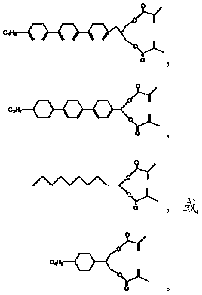
- 一种液晶显示面板的制作方法,包括以下步骤:步骤1、将热敏型交联材料混入液晶材料中,得到液晶混合物;所述热敏型交联材料的结构通式为其中,
 A是
A是 B是
B是 R是具有5~20个C原子的直链或支链化的烷基、该烷基中的某个CH2基团被苯基、环烷基、-O-、-CONH-、-COO-、-O-CO-、-CO-或-CH=CH-基团所取代后得到的第一基团、或者该烷基和该第一基团中的某个H原子被F或Cl原子取代后得到的第二基团;步骤2、提供TFT基板,采用滴下式注入法将所述步骤1得到的液晶混合物滴加到TFT基板的一侧上;步骤3、提供CF基板,采用滴下式注入法在所述CF基板的一侧上滴加框胶,形成封框胶;步骤4、将TFT基板与CF基板进行真空对组,此时,封框胶与液晶混合物位于所述TFT基板与CF基板之间,得到液晶盒;步骤5、对步骤4中得到的液晶盒进行紫外光照射,然后进行加热,以使封框胶固化,在加热过程中,液晶混合物中的热敏型交联材料会发生交联反应而形成聚合物,随着聚合物分子量的增加,聚合物与液晶材料发生相分离,从而沉积在TFT基板和CF基板的相对一侧的表面而形成配向膜,其中聚合物中的可与液晶相容的支链部分R可以起到垂直配向的效果。
 - 如权利要求3所述的液晶显示面板的制作方法,其中,所述热敏型交联材料的结构式为:

- 如权利要求3所述的液晶显示面板的制作方法,其中,所述步骤1得到的液晶混合物中,所述热敏型交联材料的含量为0.1~5wt%。
- 如权利要求3所述的液晶显示面板的制作方法,其中,所述步骤5中,紫外光的照射强度为50~100mW/cm2,照射时间为1~5min,加热的温度为110~130℃,加热时间为20~30min。
- 如权利要求3所述的液晶显示面板的制作方法,其中,所制作的液晶显示面板为多畴垂直取向型液晶显示面板,所述步骤2中提供的TFT基板预滴加液晶混合物的一侧上设有数个屋脊状的凸起物,所述步骤3中提供的CF基板预滴加框胶的一侧上设有数个屋脊状的凸起物。
- 如权利要求3所述的液晶显示面板的制作方法,其中,所述步骤2中提供的TFT基板预滴加液晶混合物的一侧上设有像素电极,所述步骤3中提供的CF基板预滴加框胶的一侧上设有公共电极。
- 一种液晶显示面板,包括相对设置的TFT基板与CF基板、夹设于TFT基板与CF基板之间的液晶层、用于密封TFT基板与CF基板的封框胶、及形成于所述TFT基板与CF基板朝向液晶层一侧表面的配向膜;所述TFT基板与CF基板朝向液晶层的一侧上设有数个屋脊状的凸起物;所述液晶层包括液晶材料;所述配向膜为混合于液晶材料中的热敏型交联材料在加热条件下发生交联反应而形成并沉积在所述TFT基板与CF基板的相对一侧的表面的聚合物;所述热敏型交联材料的结构通式为其中,
 A是
A是 B是
B是 R是具有5~20个C原子的直链或支链化的烷基、该烷基中的某个CH2基团被苯基、环烷基、-O-、-CONH-、-COO-、-O-CO-、-CO-或-CH=CH-基团所取代后得到的第一基团、或者该烷基和该第一基团中的某个H原子被F或Cl原子取代后得到的基团。
 - 如权利要求9所述的液晶显示面板,其中,所述热敏型交联材料 的结构式为:

Priority Applications (1)
| Application Number | Priority Date | Filing Date | Title |
|---|---|---|---|
| US15/026,255 US10303001B2 (en) | 2016-01-29 | 2016-02-26 | Thermal crosslink material, manufacture method of liquid crystal display panel and liquid crystal display panel |
Applications Claiming Priority (2)
| Application Number | Priority Date | Filing Date | Title |
|---|---|---|---|
| CN201610070586.8 | 2016-01-29 | ||
| CN201610070586.8A CN105647547B (zh) | 2016-01-29 | 2016-01-29 | 热敏型交联材料、液晶显示面板的制作方法及液晶显示面板 |
Publications (1)
| Publication Number | Publication Date |
|---|---|
| WO2017128472A1 true WO2017128472A1 (zh) | 2017-08-03 |
Family
ID=56489032
Family Applications (1)
| Application Number | Title | Priority Date | Filing Date |
|---|---|---|---|
| PCT/CN2016/074615 Ceased WO2017128472A1 (zh) | 2016-01-29 | 2016-02-26 | 热敏型交联材料、液晶显示面板的制作方法及液晶显示面板 |
Country Status (3)
| Country | Link |
|---|---|
| US (3) | US10303001B2 (zh) |
| CN (1) | CN105647547B (zh) |
| WO (1) | WO2017128472A1 (zh) |
Cited By (2)
| Publication number | Priority date | Publication date | Assignee | Title |
|---|---|---|---|---|
| WO2017209161A1 (ja) * | 2016-06-03 | 2017-12-07 | Jnc株式会社 | 重合性極性化合物、液晶組成物、および液晶表示素子 |
| JP2019099572A (ja) * | 2017-12-06 | 2019-06-24 | Jnc株式会社 | 化合物、液晶組成物、および液晶表示素子 |
Families Citing this family (4)
| Publication number | Priority date | Publication date | Assignee | Title |
|---|---|---|---|---|
| KR20200084327A (ko) * | 2017-11-17 | 2020-07-10 | 디아이씨 가부시끼가이샤 | 중합성 화합물과, 그것을 사용한 액정 조성물 및 액정 표시 소자 |
| WO2019167640A1 (ja) | 2018-03-01 | 2019-09-06 | Dic株式会社 | 重合性化合物並びにそれを使用した液晶組成物及び液晶表示素子 |
| CN110358547A (zh) * | 2018-04-10 | 2019-10-22 | 北京八亿时空液晶科技股份有限公司 | 一种新型可聚合性化合物及其应用 |
| CN110187564A (zh) * | 2019-05-21 | 2019-08-30 | 深圳市华星光电技术有限公司 | 一种显示面板及其制备方法 |
Family Cites Families (13)
| Publication number | Priority date | Publication date | Assignee | Title |
|---|---|---|---|---|
| US3972589A (en) * | 1972-06-23 | 1976-08-03 | General Electric Company | Nematic liquid crystal mixtures with stable homeotropic boundary conditions and methods of making the same |
| JP2750964B2 (ja) * | 1991-05-24 | 1998-05-18 | 三ツ星ベルト株式会社 | 繊維材料に加硫接着良好なゴム組成物 |
| JP2868188B2 (ja) * | 1991-05-31 | 1999-03-10 | 日本化薬株式会社 | (メタ)アクリル酸エステル、その製造方法、それを用いた樹脂組成物、光ファイバー用コーティング剤及び硬化物 |
| JP2007063155A (ja) * | 2005-08-29 | 2007-03-15 | Hyogo Prefecture | 液晶性重合性低分子化合物、該化合物を用いた複屈折性フィルム及び複屈折性セル、並びにこれらの製造方法 |
| US20130299741A1 (en) * | 2012-05-09 | 2013-11-14 | Shenzhen China Star Optoelectronics Technology Co. Ltd. | Liquid crystal medium composition |
| CN102876335B (zh) * | 2012-09-21 | 2014-07-16 | 深圳市华星光电技术有限公司 | 液晶介质混合物及使用其的液晶显示器 |
| CN102888229B (zh) * | 2012-09-21 | 2014-07-16 | 深圳市华星光电技术有限公司 | 液晶介质混合物及使用其的液晶显示器 |
| CN102863969B (zh) * | 2012-09-21 | 2014-07-16 | 深圳市华星光电技术有限公司 | 液晶介质混合物及使用其的液晶显示器 |
| CN102911052B (zh) * | 2012-10-13 | 2015-03-25 | 江苏和成显示科技股份有限公司 | 聚合性星形化合物及其聚合产物和在液晶装置中的应用 |
| KR102314014B1 (ko) * | 2013-09-24 | 2021-10-19 | 엔탑시스, 엘엘씨 | 검출 가능한 어레이들, 진단을 위한 시스템들, 및 이를 만들고 사용하는 방법들 |
| CN104845644B (zh) * | 2015-05-27 | 2017-03-15 | 深圳市华星光电技术有限公司 | 一种液晶介质组合物 |
| CN105087021B (zh) * | 2015-06-18 | 2017-11-17 | 深圳市华星光电技术有限公司 | 一种液晶垂直取向剂、液晶显示元件以及液晶显示元件的制备方法 |
| CN105061213B (zh) * | 2015-08-24 | 2017-05-17 | 江苏和成新材料有限公司 | 具有四原子桥键的可聚合化合物及其制备方法及应用 |
-
2016
- 2016-01-29 CN CN201610070586.8A patent/CN105647547B/zh active Active
- 2016-02-26 WO PCT/CN2016/074615 patent/WO2017128472A1/zh not_active Ceased
- 2016-02-26 US US15/026,255 patent/US10303001B2/en active Active
-
2019
- 2019-03-11 US US16/297,710 patent/US10824017B2/en active Active
- 2019-03-11 US US16/297,712 patent/US10824018B2/en active Active
Non-Patent Citations (1)
| Title |
|---|
| DATABASE Registry 23 April 1993 (1993-04-23), Database accession no. 147187-60-8 * |
Cited By (3)
| Publication number | Priority date | Publication date | Assignee | Title |
|---|---|---|---|---|
| WO2017209161A1 (ja) * | 2016-06-03 | 2017-12-07 | Jnc株式会社 | 重合性極性化合物、液晶組成物、および液晶表示素子 |
| JP2019099572A (ja) * | 2017-12-06 | 2019-06-24 | Jnc株式会社 | 化合物、液晶組成物、および液晶表示素子 |
| JP7143741B2 (ja) | 2017-12-06 | 2022-09-29 | Jnc株式会社 | 化合物、液晶組成物、および液晶表示素子 |
Also Published As
| Publication number | Publication date |
|---|---|
| US20190204635A1 (en) | 2019-07-04 |
| US20180045991A1 (en) | 2018-02-15 |
| US20190204636A1 (en) | 2019-07-04 |
| CN105647547A (zh) | 2016-06-08 |
| CN105647547B (zh) | 2018-06-05 |
| US10824017B2 (en) | 2020-11-03 |
| US10303001B2 (en) | 2019-05-28 |
| US10824018B2 (en) | 2020-11-03 |
Similar Documents
| Publication | Publication Date | Title |
|---|---|---|
| WO2017128472A1 (zh) | 热敏型交联材料、液晶显示面板的制作方法及液晶显示面板 | |
| US9146425B2 (en) | Liquid crystal display and method of manufacturing the same | |
| US5705096A (en) | UV crosslinking compound, alignment film for LCD component and LCD component | |
| US9034567B2 (en) | Method for manufacturing liquid crystal display device, and liquid crystal display device | |
| CN101042505B (zh) | 垂直液晶取向剂和垂直液晶显示元件 | |
| US20150022750A1 (en) | Liquid crystal display device and method for producing the same | |
| US9771517B2 (en) | Liquid-crystal optical modulation element | |
| TWI678391B (zh) | 液晶配向劑、液晶配向膜及液晶顯示元件 | |
| US9250476B2 (en) | Liquid crystal display device and method for producing the same | |
| WO2017084154A1 (zh) | 反应型垂直取向材料、液晶显示面板、及液晶配向方法 | |
| WO2016201720A1 (zh) | 一种液晶垂直取向剂、液晶显示元件以及液晶显示元件的制备方法 | |
| TW200919043A (en) | Method for manufacturing liquid crystal display | |
| JPH10232400A (ja) | 光配向性組成物、これから形成される配向膜とこの配向膜を具備した液晶表示素子 | |
| CN101923251B (zh) | 液晶显示器基板配向处理方法及液晶显示器制造方法 | |
| WO2020107777A1 (zh) | 液晶显示面板的制作方法及液晶显示面板 | |
| WO2017084147A1 (zh) | 反应型垂直取向有机硅材料及液晶显示面板的制作方法 | |
| JP4429334B2 (ja) | 液晶表示パネル及びその製造方法 | |
| TWI628219B (zh) | 具有橫向電場驅動型液晶顯示元件用液晶配向膜之基板的製造方法 | |
| KR20130050862A (ko) | 액정 표시 장치 및 그 제조 방법 | |
| US5725915A (en) | Liquid crystal display | |
| US7468198B2 (en) | Liquid crystal compound, ferroelectric liquid crystal composition, and ferroelectric liquid crystal display | |
| JP3095506B2 (ja) | 液晶混合物およびこれを用いた液晶表示素子 | |
| US20170090252A1 (en) | Liquid crystal horizontal orientation agent, horizontal orientation type liquid crystal composition, and horizontal orientation type liquid crystal display device and method of fabricating the same | |
| JPH08254688A (ja) | 液晶表示素子 | |
| KR101373462B1 (ko) | 폴리카보네이트계 감광성 액정 배향제 조성물, 이를 이용한액정 배향막 및 그 제조방법과 액정 배향막을 구비한액정표시장치 및 그 제조방법 |
Legal Events
| Date | Code | Title | Description |
|---|---|---|---|
| WWE | Wipo information: entry into national phase |
Ref document number: 15026255 Country of ref document: US |
|
| 121 | Ep: the epo has been informed by wipo that ep was designated in this application |
Ref document number: 16887356 Country of ref document: EP Kind code of ref document: A1 |
|
| NENP | Non-entry into the national phase |
Ref country code: DE |
|
| 122 | Ep: pct application non-entry in european phase |
Ref document number: 16887356 Country of ref document: EP Kind code of ref document: A1 |