WO2017126653A1 - 接合体、パワーモジュール用基板、パワーモジュール、接合体の製造方法及びパワーモジュール用基板の製造方法 - Google Patents
接合体、パワーモジュール用基板、パワーモジュール、接合体の製造方法及びパワーモジュール用基板の製造方法 Download PDFInfo
- Publication number
- WO2017126653A1 WO2017126653A1 PCT/JP2017/001922 JP2017001922W WO2017126653A1 WO 2017126653 A1 WO2017126653 A1 WO 2017126653A1 JP 2017001922 W JP2017001922 W JP 2017001922W WO 2017126653 A1 WO2017126653 A1 WO 2017126653A1
- Authority
- WO
- WIPO (PCT)
- Prior art keywords
- ceramic substrate
- power module
- substrate
- ceramic
- circuit layer
- Prior art date
Links
Images


Classifications
-
- H—ELECTRICITY
- H01—ELECTRIC ELEMENTS
- H01L—SEMICONDUCTOR DEVICES NOT COVERED BY CLASS H10
- H01L23/00—Details of semiconductor or other solid state devices
- H01L23/34—Arrangements for cooling, heating, ventilating or temperature compensation ; Temperature sensing arrangements
- H01L23/36—Selection of materials, or shaping, to facilitate cooling or heating, e.g. heatsinks
- H01L23/373—Cooling facilitated by selection of materials for the device or materials for thermal expansion adaptation, e.g. carbon
- H01L23/3735—Laminates or multilayers, e.g. direct bond copper ceramic substrates
-
- H—ELECTRICITY
- H01—ELECTRIC ELEMENTS
- H01L—SEMICONDUCTOR DEVICES NOT COVERED BY CLASS H10
- H01L23/00—Details of semiconductor or other solid state devices
- H01L23/52—Arrangements for conducting electric current within the device in operation from one component to another, i.e. interconnections, e.g. wires, lead frames
- H01L23/522—Arrangements for conducting electric current within the device in operation from one component to another, i.e. interconnections, e.g. wires, lead frames including external interconnections consisting of a multilayer structure of conductive and insulating layers inseparably formed on the semiconductor body
- H01L23/532—Arrangements for conducting electric current within the device in operation from one component to another, i.e. interconnections, e.g. wires, lead frames including external interconnections consisting of a multilayer structure of conductive and insulating layers inseparably formed on the semiconductor body characterised by the materials
- H01L23/53204—Conductive materials
- H01L23/53209—Conductive materials based on metals, e.g. alloys, metal silicides
- H01L23/53228—Conductive materials based on metals, e.g. alloys, metal silicides the principal metal being copper
-
- B—PERFORMING OPERATIONS; TRANSPORTING
- B23—MACHINE TOOLS; METAL-WORKING NOT OTHERWISE PROVIDED FOR
- B23K—SOLDERING OR UNSOLDERING; WELDING; CLADDING OR PLATING BY SOLDERING OR WELDING; CUTTING BY APPLYING HEAT LOCALLY, e.g. FLAME CUTTING; WORKING BY LASER BEAM
- B23K1/00—Soldering, e.g. brazing, or unsoldering
- B23K1/008—Soldering within a furnace
-
- B—PERFORMING OPERATIONS; TRANSPORTING
- B23—MACHINE TOOLS; METAL-WORKING NOT OTHERWISE PROVIDED FOR
- B23K—SOLDERING OR UNSOLDERING; WELDING; CLADDING OR PLATING BY SOLDERING OR WELDING; CUTTING BY APPLYING HEAT LOCALLY, e.g. FLAME CUTTING; WORKING BY LASER BEAM
- B23K35/00—Rods, electrodes, materials, or media, for use in soldering, welding, or cutting
- B23K35/02—Rods, electrodes, materials, or media, for use in soldering, welding, or cutting characterised by mechanical features, e.g. shape
- B23K35/0222—Rods, electrodes, materials, or media, for use in soldering, welding, or cutting characterised by mechanical features, e.g. shape for use in soldering, brazing
- B23K35/0233—Sheets, foils
- B23K35/0238—Sheets, foils layered
-
- B—PERFORMING OPERATIONS; TRANSPORTING
- B23—MACHINE TOOLS; METAL-WORKING NOT OTHERWISE PROVIDED FOR
- B23K—SOLDERING OR UNSOLDERING; WELDING; CLADDING OR PLATING BY SOLDERING OR WELDING; CUTTING BY APPLYING HEAT LOCALLY, e.g. FLAME CUTTING; WORKING BY LASER BEAM
- B23K35/00—Rods, electrodes, materials, or media, for use in soldering, welding, or cutting
- B23K35/22—Rods, electrodes, materials, or media, for use in soldering, welding, or cutting characterised by the composition or nature of the material
- B23K35/24—Selection of soldering or welding materials proper
- B23K35/26—Selection of soldering or welding materials proper with the principal constituent melting at less than 400 degrees C
- B23K35/262—Sn as the principal constituent
-
- B—PERFORMING OPERATIONS; TRANSPORTING
- B23—MACHINE TOOLS; METAL-WORKING NOT OTHERWISE PROVIDED FOR
- B23K—SOLDERING OR UNSOLDERING; WELDING; CLADDING OR PLATING BY SOLDERING OR WELDING; CUTTING BY APPLYING HEAT LOCALLY, e.g. FLAME CUTTING; WORKING BY LASER BEAM
- B23K35/00—Rods, electrodes, materials, or media, for use in soldering, welding, or cutting
- B23K35/22—Rods, electrodes, materials, or media, for use in soldering, welding, or cutting characterised by the composition or nature of the material
- B23K35/24—Selection of soldering or welding materials proper
- B23K35/30—Selection of soldering or welding materials proper with the principal constituent melting at less than 1550 degrees C
- B23K35/302—Cu as the principal constituent
-
- C—CHEMISTRY; METALLURGY
- C04—CEMENTS; CONCRETE; ARTIFICIAL STONE; CERAMICS; REFRACTORIES
- C04B—LIME, MAGNESIA; SLAG; CEMENTS; COMPOSITIONS THEREOF, e.g. MORTARS, CONCRETE OR LIKE BUILDING MATERIALS; ARTIFICIAL STONE; CERAMICS; REFRACTORIES; TREATMENT OF NATURAL STONE
- C04B35/00—Shaped ceramic products characterised by their composition; Ceramics compositions; Processing powders of inorganic compounds preparatory to the manufacturing of ceramic products
- C04B35/515—Shaped ceramic products characterised by their composition; Ceramics compositions; Processing powders of inorganic compounds preparatory to the manufacturing of ceramic products based on non-oxide ceramics
- C04B35/58—Shaped ceramic products characterised by their composition; Ceramics compositions; Processing powders of inorganic compounds preparatory to the manufacturing of ceramic products based on non-oxide ceramics based on borides, nitrides, i.e. nitrides, oxynitrides, carbonitrides or oxycarbonitrides or silicides
- C04B35/581—Shaped ceramic products characterised by their composition; Ceramics compositions; Processing powders of inorganic compounds preparatory to the manufacturing of ceramic products based on non-oxide ceramics based on borides, nitrides, i.e. nitrides, oxynitrides, carbonitrides or oxycarbonitrides or silicides based on aluminium nitride
-
- C—CHEMISTRY; METALLURGY
- C04—CEMENTS; CONCRETE; ARTIFICIAL STONE; CERAMICS; REFRACTORIES
- C04B—LIME, MAGNESIA; SLAG; CEMENTS; COMPOSITIONS THEREOF, e.g. MORTARS, CONCRETE OR LIKE BUILDING MATERIALS; ARTIFICIAL STONE; CERAMICS; REFRACTORIES; TREATMENT OF NATURAL STONE
- C04B35/00—Shaped ceramic products characterised by their composition; Ceramics compositions; Processing powders of inorganic compounds preparatory to the manufacturing of ceramic products
- C04B35/622—Forming processes; Processing powders of inorganic compounds preparatory to the manufacturing of ceramic products
- C04B35/64—Burning or sintering processes
- C04B35/645—Pressure sintering
-
- C—CHEMISTRY; METALLURGY
- C04—CEMENTS; CONCRETE; ARTIFICIAL STONE; CERAMICS; REFRACTORIES
- C04B—LIME, MAGNESIA; SLAG; CEMENTS; COMPOSITIONS THEREOF, e.g. MORTARS, CONCRETE OR LIKE BUILDING MATERIALS; ARTIFICIAL STONE; CERAMICS; REFRACTORIES; TREATMENT OF NATURAL STONE
- C04B37/00—Joining burned ceramic articles with other burned ceramic articles or other articles by heating
- C04B37/02—Joining burned ceramic articles with other burned ceramic articles or other articles by heating with metallic articles
- C04B37/023—Joining burned ceramic articles with other burned ceramic articles or other articles by heating with metallic articles characterised by the interlayer used
- C04B37/026—Joining burned ceramic articles with other burned ceramic articles or other articles by heating with metallic articles characterised by the interlayer used consisting of metals or metal salts
-
- C—CHEMISTRY; METALLURGY
- C22—METALLURGY; FERROUS OR NON-FERROUS ALLOYS; TREATMENT OF ALLOYS OR NON-FERROUS METALS
- C22C—ALLOYS
- C22C9/00—Alloys based on copper
- C22C9/02—Alloys based on copper with tin as the next major constituent
-
- H—ELECTRICITY
- H01—ELECTRIC ELEMENTS
- H01L—SEMICONDUCTOR DEVICES NOT COVERED BY CLASS H10
- H01L21/00—Processes or apparatus adapted for the manufacture or treatment of semiconductor or solid state devices or of parts thereof
- H01L21/02—Manufacture or treatment of semiconductor devices or of parts thereof
- H01L21/04—Manufacture or treatment of semiconductor devices or of parts thereof the devices having at least one potential-jump barrier or surface barrier, e.g. PN junction, depletion layer or carrier concentration layer
- H01L21/48—Manufacture or treatment of parts, e.g. containers, prior to assembly of the devices, using processes not provided for in a single one of the subgroups H01L21/06 - H01L21/326
- H01L21/4814—Conductive parts
- H01L21/4871—Bases, plates or heatsinks
- H01L21/4882—Assembly of heatsink parts
-
- H—ELECTRICITY
- H01—ELECTRIC ELEMENTS
- H01L—SEMICONDUCTOR DEVICES NOT COVERED BY CLASS H10
- H01L23/00—Details of semiconductor or other solid state devices
- H01L23/12—Mountings, e.g. non-detachable insulating substrates
- H01L23/14—Mountings, e.g. non-detachable insulating substrates characterised by the material or its electrical properties
- H01L23/142—Metallic substrates having insulating layers
-
- H—ELECTRICITY
- H01—ELECTRIC ELEMENTS
- H01L—SEMICONDUCTOR DEVICES NOT COVERED BY CLASS H10
- H01L23/00—Details of semiconductor or other solid state devices
- H01L23/34—Arrangements for cooling, heating, ventilating or temperature compensation ; Temperature sensing arrangements
- H01L23/36—Selection of materials, or shaping, to facilitate cooling or heating, e.g. heatsinks
- H01L23/373—Cooling facilitated by selection of materials for the device or materials for thermal expansion adaptation, e.g. carbon
- H01L23/3731—Ceramic materials or glass
-
- H—ELECTRICITY
- H01—ELECTRIC ELEMENTS
- H01L—SEMICONDUCTOR DEVICES NOT COVERED BY CLASS H10
- H01L23/00—Details of semiconductor or other solid state devices
- H01L23/34—Arrangements for cooling, heating, ventilating or temperature compensation ; Temperature sensing arrangements
- H01L23/36—Selection of materials, or shaping, to facilitate cooling or heating, e.g. heatsinks
- H01L23/373—Cooling facilitated by selection of materials for the device or materials for thermal expansion adaptation, e.g. carbon
- H01L23/3736—Metallic materials
-
- B—PERFORMING OPERATIONS; TRANSPORTING
- B23—MACHINE TOOLS; METAL-WORKING NOT OTHERWISE PROVIDED FOR
- B23K—SOLDERING OR UNSOLDERING; WELDING; CLADDING OR PLATING BY SOLDERING OR WELDING; CUTTING BY APPLYING HEAT LOCALLY, e.g. FLAME CUTTING; WORKING BY LASER BEAM
- B23K2101/00—Articles made by soldering, welding or cutting
- B23K2101/36—Electric or electronic devices
- B23K2101/40—Semiconductor devices
-
- B—PERFORMING OPERATIONS; TRANSPORTING
- B23—MACHINE TOOLS; METAL-WORKING NOT OTHERWISE PROVIDED FOR
- B23K—SOLDERING OR UNSOLDERING; WELDING; CLADDING OR PLATING BY SOLDERING OR WELDING; CUTTING BY APPLYING HEAT LOCALLY, e.g. FLAME CUTTING; WORKING BY LASER BEAM
- B23K2103/00—Materials to be soldered, welded or cut
- B23K2103/16—Composite materials, e.g. fibre reinforced
- B23K2103/166—Multilayered materials
- B23K2103/172—Multilayered materials wherein at least one of the layers is non-metallic
-
- C—CHEMISTRY; METALLURGY
- C04—CEMENTS; CONCRETE; ARTIFICIAL STONE; CERAMICS; REFRACTORIES
- C04B—LIME, MAGNESIA; SLAG; CEMENTS; COMPOSITIONS THEREOF, e.g. MORTARS, CONCRETE OR LIKE BUILDING MATERIALS; ARTIFICIAL STONE; CERAMICS; REFRACTORIES; TREATMENT OF NATURAL STONE
- C04B2235/00—Aspects relating to ceramic starting mixtures or sintered ceramic products
- C04B2235/02—Composition of constituents of the starting material or of secondary phases of the final product
- C04B2235/30—Constituents and secondary phases not being of a fibrous nature
- C04B2235/32—Metal oxides, mixed metal oxides, or oxide-forming salts thereof, e.g. carbonates, nitrates, (oxy)hydroxides, chlorides
- C04B2235/3231—Refractory metal oxides, their mixed metal oxides, or oxide-forming salts thereof
- C04B2235/3244—Zirconium oxides, zirconates, hafnium oxides, hafnates, or oxide-forming salts thereof
-
- C—CHEMISTRY; METALLURGY
- C04—CEMENTS; CONCRETE; ARTIFICIAL STONE; CERAMICS; REFRACTORIES
- C04B—LIME, MAGNESIA; SLAG; CEMENTS; COMPOSITIONS THEREOF, e.g. MORTARS, CONCRETE OR LIKE BUILDING MATERIALS; ARTIFICIAL STONE; CERAMICS; REFRACTORIES; TREATMENT OF NATURAL STONE
- C04B2235/00—Aspects relating to ceramic starting mixtures or sintered ceramic products
- C04B2235/65—Aspects relating to heat treatments of ceramic bodies such as green ceramics or pre-sintered ceramics, e.g. burning, sintering or melting processes
- C04B2235/656—Aspects relating to heat treatments of ceramic bodies such as green ceramics or pre-sintered ceramics, e.g. burning, sintering or melting processes characterised by specific heating conditions during heat treatment
- C04B2235/6562—Heating rate
-
- C—CHEMISTRY; METALLURGY
- C04—CEMENTS; CONCRETE; ARTIFICIAL STONE; CERAMICS; REFRACTORIES
- C04B—LIME, MAGNESIA; SLAG; CEMENTS; COMPOSITIONS THEREOF, e.g. MORTARS, CONCRETE OR LIKE BUILDING MATERIALS; ARTIFICIAL STONE; CERAMICS; REFRACTORIES; TREATMENT OF NATURAL STONE
- C04B2235/00—Aspects relating to ceramic starting mixtures or sintered ceramic products
- C04B2235/65—Aspects relating to heat treatments of ceramic bodies such as green ceramics or pre-sintered ceramics, e.g. burning, sintering or melting processes
- C04B2235/656—Aspects relating to heat treatments of ceramic bodies such as green ceramics or pre-sintered ceramics, e.g. burning, sintering or melting processes characterised by specific heating conditions during heat treatment
- C04B2235/6567—Treatment time
-
- C—CHEMISTRY; METALLURGY
- C04—CEMENTS; CONCRETE; ARTIFICIAL STONE; CERAMICS; REFRACTORIES
- C04B—LIME, MAGNESIA; SLAG; CEMENTS; COMPOSITIONS THEREOF, e.g. MORTARS, CONCRETE OR LIKE BUILDING MATERIALS; ARTIFICIAL STONE; CERAMICS; REFRACTORIES; TREATMENT OF NATURAL STONE
- C04B2237/00—Aspects relating to ceramic laminates or to joining of ceramic articles with other articles by heating
- C04B2237/02—Aspects relating to interlayers, e.g. used to join ceramic articles with other articles by heating
- C04B2237/12—Metallic interlayers
- C04B2237/121—Metallic interlayers based on aluminium
-
- C—CHEMISTRY; METALLURGY
- C04—CEMENTS; CONCRETE; ARTIFICIAL STONE; CERAMICS; REFRACTORIES
- C04B—LIME, MAGNESIA; SLAG; CEMENTS; COMPOSITIONS THEREOF, e.g. MORTARS, CONCRETE OR LIKE BUILDING MATERIALS; ARTIFICIAL STONE; CERAMICS; REFRACTORIES; TREATMENT OF NATURAL STONE
- C04B2237/00—Aspects relating to ceramic laminates or to joining of ceramic articles with other articles by heating
- C04B2237/02—Aspects relating to interlayers, e.g. used to join ceramic articles with other articles by heating
- C04B2237/12—Metallic interlayers
- C04B2237/122—Metallic interlayers based on refractory metals
-
- C—CHEMISTRY; METALLURGY
- C04—CEMENTS; CONCRETE; ARTIFICIAL STONE; CERAMICS; REFRACTORIES
- C04B—LIME, MAGNESIA; SLAG; CEMENTS; COMPOSITIONS THEREOF, e.g. MORTARS, CONCRETE OR LIKE BUILDING MATERIALS; ARTIFICIAL STONE; CERAMICS; REFRACTORIES; TREATMENT OF NATURAL STONE
- C04B2237/00—Aspects relating to ceramic laminates or to joining of ceramic articles with other articles by heating
- C04B2237/02—Aspects relating to interlayers, e.g. used to join ceramic articles with other articles by heating
- C04B2237/12—Metallic interlayers
- C04B2237/124—Metallic interlayers based on copper
-
- C—CHEMISTRY; METALLURGY
- C04—CEMENTS; CONCRETE; ARTIFICIAL STONE; CERAMICS; REFRACTORIES
- C04B—LIME, MAGNESIA; SLAG; CEMENTS; COMPOSITIONS THEREOF, e.g. MORTARS, CONCRETE OR LIKE BUILDING MATERIALS; ARTIFICIAL STONE; CERAMICS; REFRACTORIES; TREATMENT OF NATURAL STONE
- C04B2237/00—Aspects relating to ceramic laminates or to joining of ceramic articles with other articles by heating
- C04B2237/02—Aspects relating to interlayers, e.g. used to join ceramic articles with other articles by heating
- C04B2237/12—Metallic interlayers
- C04B2237/126—Metallic interlayers wherein the active component for bonding is not the largest fraction of the interlayer
- C04B2237/127—The active component for bonding being a refractory metal
-
- C—CHEMISTRY; METALLURGY
- C04—CEMENTS; CONCRETE; ARTIFICIAL STONE; CERAMICS; REFRACTORIES
- C04B—LIME, MAGNESIA; SLAG; CEMENTS; COMPOSITIONS THEREOF, e.g. MORTARS, CONCRETE OR LIKE BUILDING MATERIALS; ARTIFICIAL STONE; CERAMICS; REFRACTORIES; TREATMENT OF NATURAL STONE
- C04B2237/00—Aspects relating to ceramic laminates or to joining of ceramic articles with other articles by heating
- C04B2237/02—Aspects relating to interlayers, e.g. used to join ceramic articles with other articles by heating
- C04B2237/12—Metallic interlayers
- C04B2237/126—Metallic interlayers wherein the active component for bonding is not the largest fraction of the interlayer
- C04B2237/128—The active component for bonding being silicon
-
- C—CHEMISTRY; METALLURGY
- C04—CEMENTS; CONCRETE; ARTIFICIAL STONE; CERAMICS; REFRACTORIES
- C04B—LIME, MAGNESIA; SLAG; CEMENTS; COMPOSITIONS THEREOF, e.g. MORTARS, CONCRETE OR LIKE BUILDING MATERIALS; ARTIFICIAL STONE; CERAMICS; REFRACTORIES; TREATMENT OF NATURAL STONE
- C04B2237/00—Aspects relating to ceramic laminates or to joining of ceramic articles with other articles by heating
- C04B2237/30—Composition of layers of ceramic laminates or of ceramic or metallic articles to be joined by heating, e.g. Si substrates
- C04B2237/32—Ceramic
- C04B2237/36—Non-oxidic
- C04B2237/366—Aluminium nitride
-
- C—CHEMISTRY; METALLURGY
- C04—CEMENTS; CONCRETE; ARTIFICIAL STONE; CERAMICS; REFRACTORIES
- C04B—LIME, MAGNESIA; SLAG; CEMENTS; COMPOSITIONS THEREOF, e.g. MORTARS, CONCRETE OR LIKE BUILDING MATERIALS; ARTIFICIAL STONE; CERAMICS; REFRACTORIES; TREATMENT OF NATURAL STONE
- C04B2237/00—Aspects relating to ceramic laminates or to joining of ceramic articles with other articles by heating
- C04B2237/30—Composition of layers of ceramic laminates or of ceramic or metallic articles to be joined by heating, e.g. Si substrates
- C04B2237/40—Metallic
- C04B2237/402—Aluminium
-
- C—CHEMISTRY; METALLURGY
- C04—CEMENTS; CONCRETE; ARTIFICIAL STONE; CERAMICS; REFRACTORIES
- C04B—LIME, MAGNESIA; SLAG; CEMENTS; COMPOSITIONS THEREOF, e.g. MORTARS, CONCRETE OR LIKE BUILDING MATERIALS; ARTIFICIAL STONE; CERAMICS; REFRACTORIES; TREATMENT OF NATURAL STONE
- C04B2237/00—Aspects relating to ceramic laminates or to joining of ceramic articles with other articles by heating
- C04B2237/30—Composition of layers of ceramic laminates or of ceramic or metallic articles to be joined by heating, e.g. Si substrates
- C04B2237/40—Metallic
- C04B2237/407—Copper
-
- C—CHEMISTRY; METALLURGY
- C04—CEMENTS; CONCRETE; ARTIFICIAL STONE; CERAMICS; REFRACTORIES
- C04B—LIME, MAGNESIA; SLAG; CEMENTS; COMPOSITIONS THEREOF, e.g. MORTARS, CONCRETE OR LIKE BUILDING MATERIALS; ARTIFICIAL STONE; CERAMICS; REFRACTORIES; TREATMENT OF NATURAL STONE
- C04B2237/00—Aspects relating to ceramic laminates or to joining of ceramic articles with other articles by heating
- C04B2237/50—Processing aspects relating to ceramic laminates or to the joining of ceramic articles with other articles by heating
- C04B2237/70—Forming laminates or joined articles comprising layers of a specific, unusual thickness
- C04B2237/704—Forming laminates or joined articles comprising layers of a specific, unusual thickness of one or more of the ceramic layers or articles
-
- C—CHEMISTRY; METALLURGY
- C04—CEMENTS; CONCRETE; ARTIFICIAL STONE; CERAMICS; REFRACTORIES
- C04B—LIME, MAGNESIA; SLAG; CEMENTS; COMPOSITIONS THEREOF, e.g. MORTARS, CONCRETE OR LIKE BUILDING MATERIALS; ARTIFICIAL STONE; CERAMICS; REFRACTORIES; TREATMENT OF NATURAL STONE
- C04B2237/00—Aspects relating to ceramic laminates or to joining of ceramic articles with other articles by heating
- C04B2237/50—Processing aspects relating to ceramic laminates or to the joining of ceramic articles with other articles by heating
- C04B2237/70—Forming laminates or joined articles comprising layers of a specific, unusual thickness
- C04B2237/706—Forming laminates or joined articles comprising layers of a specific, unusual thickness of one or more of the metallic layers or articles
-
- C—CHEMISTRY; METALLURGY
- C04—CEMENTS; CONCRETE; ARTIFICIAL STONE; CERAMICS; REFRACTORIES
- C04B—LIME, MAGNESIA; SLAG; CEMENTS; COMPOSITIONS THEREOF, e.g. MORTARS, CONCRETE OR LIKE BUILDING MATERIALS; ARTIFICIAL STONE; CERAMICS; REFRACTORIES; TREATMENT OF NATURAL STONE
- C04B2237/00—Aspects relating to ceramic laminates or to joining of ceramic articles with other articles by heating
- C04B2237/50—Processing aspects relating to ceramic laminates or to the joining of ceramic articles with other articles by heating
- C04B2237/72—Forming laminates or joined articles comprising at least two interlayers directly next to each other
-
- C—CHEMISTRY; METALLURGY
- C04—CEMENTS; CONCRETE; ARTIFICIAL STONE; CERAMICS; REFRACTORIES
- C04B—LIME, MAGNESIA; SLAG; CEMENTS; COMPOSITIONS THEREOF, e.g. MORTARS, CONCRETE OR LIKE BUILDING MATERIALS; ARTIFICIAL STONE; CERAMICS; REFRACTORIES; TREATMENT OF NATURAL STONE
- C04B2237/00—Aspects relating to ceramic laminates or to joining of ceramic articles with other articles by heating
- C04B2237/50—Processing aspects relating to ceramic laminates or to the joining of ceramic articles with other articles by heating
- C04B2237/74—Forming laminates or joined articles comprising at least two different interlayers separated by a substrate
-
- H—ELECTRICITY
- H01—ELECTRIC ELEMENTS
- H01L—SEMICONDUCTOR DEVICES NOT COVERED BY CLASS H10
- H01L2224/00—Indexing scheme for arrangements for connecting or disconnecting semiconductor or solid-state bodies and methods related thereto as covered by H01L24/00
- H01L2224/01—Means for bonding being attached to, or being formed on, the surface to be connected, e.g. chip-to-package, die-attach, "first-level" interconnects; Manufacturing methods related thereto
- H01L2224/26—Layer connectors, e.g. plate connectors, solder or adhesive layers; Manufacturing methods related thereto
- H01L2224/28—Structure, shape, material or disposition of the layer connectors prior to the connecting process
- H01L2224/29—Structure, shape, material or disposition of the layer connectors prior to the connecting process of an individual layer connector
- H01L2224/29001—Core members of the layer connector
- H01L2224/29099—Material
- H01L2224/291—Material with a principal constituent of the material being a metal or a metalloid, e.g. boron [B], silicon [Si], germanium [Ge], arsenic [As], antimony [Sb], tellurium [Te] and polonium [Po], and alloys thereof
- H01L2224/29101—Material with a principal constituent of the material being a metal or a metalloid, e.g. boron [B], silicon [Si], germanium [Ge], arsenic [As], antimony [Sb], tellurium [Te] and polonium [Po], and alloys thereof the principal constituent melting at a temperature of less than 400°C
- H01L2224/29109—Indium [In] as principal constituent
-
- H—ELECTRICITY
- H01—ELECTRIC ELEMENTS
- H01L—SEMICONDUCTOR DEVICES NOT COVERED BY CLASS H10
- H01L2224/00—Indexing scheme for arrangements for connecting or disconnecting semiconductor or solid-state bodies and methods related thereto as covered by H01L24/00
- H01L2224/01—Means for bonding being attached to, or being formed on, the surface to be connected, e.g. chip-to-package, die-attach, "first-level" interconnects; Manufacturing methods related thereto
- H01L2224/26—Layer connectors, e.g. plate connectors, solder or adhesive layers; Manufacturing methods related thereto
- H01L2224/28—Structure, shape, material or disposition of the layer connectors prior to the connecting process
- H01L2224/29—Structure, shape, material or disposition of the layer connectors prior to the connecting process of an individual layer connector
- H01L2224/29001—Core members of the layer connector
- H01L2224/29099—Material
- H01L2224/291—Material with a principal constituent of the material being a metal or a metalloid, e.g. boron [B], silicon [Si], germanium [Ge], arsenic [As], antimony [Sb], tellurium [Te] and polonium [Po], and alloys thereof
- H01L2224/29101—Material with a principal constituent of the material being a metal or a metalloid, e.g. boron [B], silicon [Si], germanium [Ge], arsenic [As], antimony [Sb], tellurium [Te] and polonium [Po], and alloys thereof the principal constituent melting at a temperature of less than 400°C
- H01L2224/29111—Tin [Sn] as principal constituent
-
- H—ELECTRICITY
- H01—ELECTRIC ELEMENTS
- H01L—SEMICONDUCTOR DEVICES NOT COVERED BY CLASS H10
- H01L2224/00—Indexing scheme for arrangements for connecting or disconnecting semiconductor or solid-state bodies and methods related thereto as covered by H01L24/00
- H01L2224/01—Means for bonding being attached to, or being formed on, the surface to be connected, e.g. chip-to-package, die-attach, "first-level" interconnects; Manufacturing methods related thereto
- H01L2224/26—Layer connectors, e.g. plate connectors, solder or adhesive layers; Manufacturing methods related thereto
- H01L2224/28—Structure, shape, material or disposition of the layer connectors prior to the connecting process
- H01L2224/29—Structure, shape, material or disposition of the layer connectors prior to the connecting process of an individual layer connector
- H01L2224/29001—Core members of the layer connector
- H01L2224/29099—Material
- H01L2224/291—Material with a principal constituent of the material being a metal or a metalloid, e.g. boron [B], silicon [Si], germanium [Ge], arsenic [As], antimony [Sb], tellurium [Te] and polonium [Po], and alloys thereof
- H01L2224/29138—Material with a principal constituent of the material being a metal or a metalloid, e.g. boron [B], silicon [Si], germanium [Ge], arsenic [As], antimony [Sb], tellurium [Te] and polonium [Po], and alloys thereof the principal constituent melting at a temperature of greater than or equal to 950°C and less than 1550°C
- H01L2224/29139—Silver [Ag] as principal constituent
-
- H—ELECTRICITY
- H01—ELECTRIC ELEMENTS
- H01L—SEMICONDUCTOR DEVICES NOT COVERED BY CLASS H10
- H01L2224/00—Indexing scheme for arrangements for connecting or disconnecting semiconductor or solid-state bodies and methods related thereto as covered by H01L24/00
- H01L2224/01—Means for bonding being attached to, or being formed on, the surface to be connected, e.g. chip-to-package, die-attach, "first-level" interconnects; Manufacturing methods related thereto
- H01L2224/26—Layer connectors, e.g. plate connectors, solder or adhesive layers; Manufacturing methods related thereto
- H01L2224/28—Structure, shape, material or disposition of the layer connectors prior to the connecting process
- H01L2224/29—Structure, shape, material or disposition of the layer connectors prior to the connecting process of an individual layer connector
- H01L2224/29001—Core members of the layer connector
- H01L2224/29099—Material
- H01L2224/291—Material with a principal constituent of the material being a metal or a metalloid, e.g. boron [B], silicon [Si], germanium [Ge], arsenic [As], antimony [Sb], tellurium [Te] and polonium [Po], and alloys thereof
- H01L2224/29138—Material with a principal constituent of the material being a metal or a metalloid, e.g. boron [B], silicon [Si], germanium [Ge], arsenic [As], antimony [Sb], tellurium [Te] and polonium [Po], and alloys thereof the principal constituent melting at a temperature of greater than or equal to 950°C and less than 1550°C
- H01L2224/29147—Copper [Cu] as principal constituent
-
- H—ELECTRICITY
- H01—ELECTRIC ELEMENTS
- H01L—SEMICONDUCTOR DEVICES NOT COVERED BY CLASS H10
- H01L2224/00—Indexing scheme for arrangements for connecting or disconnecting semiconductor or solid-state bodies and methods related thereto as covered by H01L24/00
- H01L2224/01—Means for bonding being attached to, or being formed on, the surface to be connected, e.g. chip-to-package, die-attach, "first-level" interconnects; Manufacturing methods related thereto
- H01L2224/26—Layer connectors, e.g. plate connectors, solder or adhesive layers; Manufacturing methods related thereto
- H01L2224/31—Structure, shape, material or disposition of the layer connectors after the connecting process
- H01L2224/32—Structure, shape, material or disposition of the layer connectors after the connecting process of an individual layer connector
- H01L2224/321—Disposition
- H01L2224/32151—Disposition the layer connector connecting between a semiconductor or solid-state body and an item not being a semiconductor or solid-state body, e.g. chip-to-substrate, chip-to-passive
- H01L2224/32221—Disposition the layer connector connecting between a semiconductor or solid-state body and an item not being a semiconductor or solid-state body, e.g. chip-to-substrate, chip-to-passive the body and the item being stacked
- H01L2224/32225—Disposition the layer connector connecting between a semiconductor or solid-state body and an item not being a semiconductor or solid-state body, e.g. chip-to-substrate, chip-to-passive the body and the item being stacked the item being non-metallic, e.g. insulating substrate with or without metallisation
- H01L2224/32227—Disposition the layer connector connecting between a semiconductor or solid-state body and an item not being a semiconductor or solid-state body, e.g. chip-to-substrate, chip-to-passive the body and the item being stacked the item being non-metallic, e.g. insulating substrate with or without metallisation the layer connector connecting to a bond pad of the item
-
- H—ELECTRICITY
- H01—ELECTRIC ELEMENTS
- H01L—SEMICONDUCTOR DEVICES NOT COVERED BY CLASS H10
- H01L2224/00—Indexing scheme for arrangements for connecting or disconnecting semiconductor or solid-state bodies and methods related thereto as covered by H01L24/00
- H01L2224/80—Methods for connecting semiconductor or other solid state bodies using means for bonding being attached to, or being formed on, the surface to be connected
- H01L2224/83—Methods for connecting semiconductor or other solid state bodies using means for bonding being attached to, or being formed on, the surface to be connected using a layer connector
- H01L2224/8338—Bonding interfaces outside the semiconductor or solid-state body
- H01L2224/83399—Material
- H01L2224/834—Material with a principal constituent of the material being a metal or a metalloid, e.g. boron [B], silicon [Si], germanium [Ge], arsenic [As], antimony [Sb], tellurium [Te] and polonium [Po], and alloys thereof
- H01L2224/83438—Material with a principal constituent of the material being a metal or a metalloid, e.g. boron [B], silicon [Si], germanium [Ge], arsenic [As], antimony [Sb], tellurium [Te] and polonium [Po], and alloys thereof the principal constituent melting at a temperature of greater than or equal to 950°C and less than 1550°C
- H01L2224/83447—Copper [Cu] as principal constituent
-
- H—ELECTRICITY
- H01—ELECTRIC ELEMENTS
- H01L—SEMICONDUCTOR DEVICES NOT COVERED BY CLASS H10
- H01L2224/00—Indexing scheme for arrangements for connecting or disconnecting semiconductor or solid-state bodies and methods related thereto as covered by H01L24/00
- H01L2224/80—Methods for connecting semiconductor or other solid state bodies using means for bonding being attached to, or being formed on, the surface to be connected
- H01L2224/83—Methods for connecting semiconductor or other solid state bodies using means for bonding being attached to, or being formed on, the surface to be connected using a layer connector
- H01L2224/838—Bonding techniques
- H01L2224/83801—Soldering or alloying
-
- H—ELECTRICITY
- H01—ELECTRIC ELEMENTS
- H01L—SEMICONDUCTOR DEVICES NOT COVERED BY CLASS H10
- H01L23/00—Details of semiconductor or other solid state devices
- H01L23/12—Mountings, e.g. non-detachable insulating substrates
- H01L23/14—Mountings, e.g. non-detachable insulating substrates characterised by the material or its electrical properties
- H01L23/15—Ceramic or glass substrates
-
- H—ELECTRICITY
- H01—ELECTRIC ELEMENTS
- H01L—SEMICONDUCTOR DEVICES NOT COVERED BY CLASS H10
- H01L24/00—Arrangements for connecting or disconnecting semiconductor or solid-state bodies; Methods or apparatus related thereto
- H01L24/01—Means for bonding being attached to, or being formed on, the surface to be connected, e.g. chip-to-package, die-attach, "first-level" interconnects; Manufacturing methods related thereto
- H01L24/26—Layer connectors, e.g. plate connectors, solder or adhesive layers; Manufacturing methods related thereto
- H01L24/28—Structure, shape, material or disposition of the layer connectors prior to the connecting process
- H01L24/29—Structure, shape, material or disposition of the layer connectors prior to the connecting process of an individual layer connector
-
- H—ELECTRICITY
- H01—ELECTRIC ELEMENTS
- H01L—SEMICONDUCTOR DEVICES NOT COVERED BY CLASS H10
- H01L24/00—Arrangements for connecting or disconnecting semiconductor or solid-state bodies; Methods or apparatus related thereto
- H01L24/01—Means for bonding being attached to, or being formed on, the surface to be connected, e.g. chip-to-package, die-attach, "first-level" interconnects; Manufacturing methods related thereto
- H01L24/26—Layer connectors, e.g. plate connectors, solder or adhesive layers; Manufacturing methods related thereto
- H01L24/31—Structure, shape, material or disposition of the layer connectors after the connecting process
- H01L24/32—Structure, shape, material or disposition of the layer connectors after the connecting process of an individual layer connector
-
- H—ELECTRICITY
- H01—ELECTRIC ELEMENTS
- H01L—SEMICONDUCTOR DEVICES NOT COVERED BY CLASS H10
- H01L24/00—Arrangements for connecting or disconnecting semiconductor or solid-state bodies; Methods or apparatus related thereto
- H01L24/80—Methods for connecting semiconductor or other solid state bodies using means for bonding being attached to, or being formed on, the surface to be connected
- H01L24/83—Methods for connecting semiconductor or other solid state bodies using means for bonding being attached to, or being formed on, the surface to be connected using a layer connector
-
- H—ELECTRICITY
- H01—ELECTRIC ELEMENTS
- H01L—SEMICONDUCTOR DEVICES NOT COVERED BY CLASS H10
- H01L2924/00—Indexing scheme for arrangements or methods for connecting or disconnecting semiconductor or solid-state bodies as covered by H01L24/00
- H01L2924/10—Details of semiconductor or other solid state devices to be connected
- H01L2924/11—Device type
- H01L2924/12—Passive devices, e.g. 2 terminal devices
- H01L2924/1204—Optical Diode
- H01L2924/12041—LED
Definitions
- the present invention relates to a joined body in which a ceramic member and a Cu member are joined, a power module substrate in which a Cu plate made of Cu or a Cu alloy is joined to a ceramic substrate, a power module including the power module substrate, and a joining
- the present invention relates to a body manufacturing method and a power module substrate manufacturing method.
- Semiconductor devices such as LEDs and power modules have a structure in which a semiconductor element is bonded on a circuit layer made of a conductive material.
- a power semiconductor element for high power control used for controlling an electric vehicle such as wind power generation or an electric vehicle
- a large amount of heat is generated. Therefore, as a substrate on which the power semiconductor element is mounted, for example, AlN (aluminum nitride) 2.
- a power module substrate in which a metal plate having excellent conductivity is bonded as a circuit layer to one surface of a ceramic substrate made of has been widely used.
- a metal plate may be joined as a metal layer to the other surface of the ceramic substrate.
- the power module substrate shown in Patent Document 1 has a structure in which a circuit layer is formed by bonding a Cu plate (Cu member) to one surface of a ceramic substrate (ceramic member).
- a Cu plate is disposed on one surface of a ceramic substrate with a Cu—Mg—Ti brazing material interposed therebetween, and heat treatment is performed to bond the Cu plate.
- an intermetallic compound containing Cu, Mg, or Ti is present in the vicinity of the ceramic substrate. It is formed.
- the intermetallic compound formed in the vicinity of the ceramic substrate is hard, the thermal stress generated in the ceramic substrate when a thermal cycle is applied to the power module substrate increases, and cracks are likely to occur in the ceramic substrate. there were.
- the bonding rate between the ceramic substrate and the circuit layer may be reduced, and it may not be possible to bond well. there were.
- Patent Documents 2 to 4 propose a power module substrate in which a ceramic substrate and a circuit layer are bonded using a Cu—P brazing material and an active element.
- P in the Cu-P brazing filler metal reacts with the active element to form a Cu layer on the ceramic substrate side, and between the hard metal in the vicinity of the ceramic substrate.
- the compound layer is not disposed. Thereby, it is possible to reduce the thermal stress generated in the ceramic substrate when a cooling cycle is applied, and to suppress the generation of cracks in the ceramic substrate.
- the present invention has been made in view of the above-described circumstances, and suppresses the occurrence of partial discharge even when a ceramic member and a Cu member are bonded well and a cooling cycle reaching a relatively high temperature is applied. It is an object of the present invention to provide a bonded body, a power module substrate comprising the bonded body, a power module, a method for manufacturing the bonded body, and a method for manufacturing the power module substrate.
- the ceramic substrate and the Cu plate are In some cases, a brittle Cu 3 P phase may be formed in the bonding layer formed between them, and when a cooling cycle reaching a relatively high temperature is applied, cracks are generated in the brittle Cu 3 P phase, and voids are formed. It was found that partial discharge is likely to occur due to the formation. Further, when the thermal cycle is loaded, cracks occur in the Cu 3 P phase, Cu 3 gaps between the P phase and the Cu-Sn layer in the bonding layer is formed, partial discharge and tends to occur Knowledge was also obtained.
- the Cu—Sn layer means that when a Cu—P brazing material containing Sn is used, P contained in the Cu—P based brazing material reacts with other elements (for example, Ti of Ti material). It is a layer formed by being consumed.
- the joined body according to one aspect of the present invention is a joined body of a ceramic member made of ceramics and a Cu member made of Cu or Cu alloy, In the bonding layer formed between the ceramic member and the Cu member, the area ratio of the Cu 3 P phase in the region from the bonding surface of the ceramic member to the Cu member side up to 50 ⁇ m is 15% or less. It is characterized by that.
- the joined body which is one aspect of the present invention, in the joining layer formed between the ceramic member and the Cu member, Cu 3 in a region from the joining surface of the ceramic member to the Cu member side up to 50 ⁇ m. Since the area ratio of the P phase is limited to 15% or less, the occurrence of partial discharge due to the Cu 3 P phase is suppressed even when a cooling cycle that reaches a relatively high temperature is loaded. Is possible.
- a power module substrate includes the above-described joined body, the ceramic substrate including the ceramic member, and the circuit layer including the Cu member formed on one surface of the ceramic substrate. And a bonding layer formed between the ceramic substrate and the circuit layer, the area ratio of the Cu 3 P phase in the region from the bonding surface of the ceramic substrate to the circuit layer side up to 50 ⁇ m is 15% or less. It is characterized by having.
- the power module substrate which is an aspect of the present invention, in the bonding layer formed between the ceramic substrate and the circuit layer, in the region of 50 ⁇ m from the bonding surface of the ceramic substrate to the circuit layer side. Since the area ratio of the Cu 3 P phase is 15% or less, even when a cooling cycle that reaches a relatively high temperature is loaded, partial discharge caused by the Cu 3 P phase is caused on the circuit layer side. Generation can be suppressed and reliability is excellent.
- a metal layer made of Al or an Al alloy may be formed on the other surface of the ceramic substrate.
- the metal layer made of Al or Al alloy having relatively small deformation resistance is formed on the other surface of the ceramic substrate, the metal layer is preferentially applied when stress is applied to the power module substrate. The stress acting on the ceramic substrate can be reduced and cracking of the ceramic substrate can be suppressed.
- a power module substrate includes the above-described joined body, the ceramic substrate including the ceramic member, a circuit layer formed on one surface of the ceramic substrate, and the ceramic substrate. And a metal layer made of the Cu member formed on the other surface, wherein a bonding layer formed between the ceramic substrate and the metal layer has a thickness of 50 ⁇ m from the bonding surface of the ceramic substrate to the metal layer side. It is characterized in that the area ratio of the Cu 3 P phase in the region up to 15% or less.
- the power module substrate which is an aspect of the present invention, in the bonding layer formed between the ceramic substrate and the metal layer, in the region from the bonding surface of the ceramic substrate to the metal layer side up to 50 ⁇ m. Since the area ratio of the Cu 3 P phase is 15% or less, even when a cooling cycle that reaches a relatively high temperature is applied, partial discharge caused by the Cu 3 P phase on the metal layer side is performed. Occurrence can be suppressed.
- a power module according to an aspect of the present invention includes the above-described power module substrate and a semiconductor element mounted on the circuit layer of the power module substrate. According to the power module having this configuration, since the power module substrate is provided in which the occurrence of partial discharge is suppressed, the power module has excellent reliability even in a usage environment in which a cooling cycle that reaches a relatively high temperature is loaded. .
- a method of manufacturing a joined body according to one aspect of the present invention is a method of manufacturing a joined body of a ceramic member made of ceramics and a Cu member made of Cu or a Cu alloy, and comprising a Cu—P brazing material and a Ti material.
- the Cu—P is added so that the atomic ratio [Ti / P] of P and Ti interposed between the ceramic member and the Cu member is in the range of 0.1 to 0.8.
- a brazing filler metal and the Ti material are disposed, and in the heat treatment step, a temperature rising rate is set in a range of 5 ° C./min to 30 ° C./min.
- the ceramic member is interposed between the Cu member and the Cu member.
- the Cu—P brazing material and the Ti material are arranged so that the atomic ratio [Ti / P] of intervening P and Ti is in the range of 0.1 to 0.8.
- the amount of Ti that reacts with P is secured, and the formation of the Cu 3 P phase can be suppressed.
- the atomic ratio [Ti / P] of P and Ti is less than 0.1, the amount of Ti that reacts with P decreases, so that the formation of a Cu 3 P phase cannot be suppressed.
- the heating rate in the heat treatment step of generating a liquid phase by heating at a temperature equal to or higher than the melting start temperature of the Cu—P brazing filler metal is 5 ° C./min or higher, Ti reacts with elements other than P. Consumption is suppressed, P reacts with Ti, and formation of a Cu 3 P phase can be suppressed.
- the temperature increase rate in the heat treatment process is 30 ° C./min or less, diffusion of Ti into the liquid phase does not occur faster than necessary, and the liquid phase becomes difficult to solidify, thereby suppressing the formation of Cu 3 P phase. can do.
- a method for manufacturing a power module substrate according to an aspect of the present invention is a method for manufacturing a power module substrate in which a circuit layer made of Cu or a Cu alloy is disposed on one surface of a ceramic substrate, the ceramic substrate And the circuit layer are bonded by the above-described manufacturing method of the bonded body.
- a power module substrate having this configuration formation of a brittle Cu 3 P phase between the ceramic substrate and the circuit layer is suppressed. Therefore, even when a cooling cycle that reaches a relatively high temperature is loaded, a power module substrate capable of suppressing the occurrence of partial discharge can be manufactured.
- a circuit layer is disposed on one surface of the ceramic substrate, and a metal layer made of Cu or a Cu alloy is disposed on the other surface of the ceramic substrate.
- a power module substrate having this configuration formation of a brittle Cu 3 P phase between the ceramic substrate and the metal layer is suppressed. Therefore, even when a cooling cycle that reaches a relatively high temperature is loaded, a power module substrate capable of suppressing the occurrence of partial discharge can be manufactured.
- a circuit layer made of Cu or a Cu alloy is disposed on one surface of a ceramic substrate, and the other surface of the ceramic substrate is made of Al or an Al alloy.
- the method for manufacturing a power module substrate having this configuration formation of a brittle Cu 3 P phase between the ceramic substrate and the circuit layer is suppressed. Therefore, manufacturing a power module substrate capable of suppressing the occurrence of partial discharge caused by the Cu 3 P phase on the circuit layer side even when a cooling cycle reaching a relatively high temperature is applied. Can do.
- the circuit layer made of Cu or Cu alloy and the ceramic substrate can be bonded at a relatively low temperature, the circuit layer made of Cu or Cu alloy, the ceramic substrate, and the metal layer made of Al or Al alloy are bonded simultaneously. It is also possible to do.
- the ceramic member and the Cu member are bonded satisfactorily, and a bonded body capable of suppressing the occurrence of partial discharge even when a cooling cycle reaching a relatively high temperature is applied, from the bonded body It is possible to provide a power module substrate, a power module, a method for manufacturing the joined body, and a method for manufacturing the power module substrate.
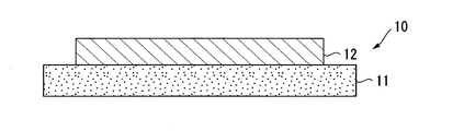
- the joined body according to the present embodiment is a power module substrate 10 in which a ceramic substrate 11 that is a ceramic member and a Cu plate 22 (circuit layer 12) that is a Cu member are joined.
- the power module 1 provided with the board
- the power module 1 includes a power module substrate 10 on which a circuit layer 12 is disposed, and a semiconductor element 3 bonded to one surface (the upper surface in FIG. 1) of the circuit layer 12 via a solder layer 2. ing.
- the power module substrate 10 includes a ceramic substrate 11 and a circuit layer 12 disposed on one surface (the upper surface in FIG. 2) of the ceramic substrate 11.
- the ceramic substrate 11 is made of ceramics such as AlN (aluminum nitride), Si 3 N 4 (silicon nitride), and Al 2 O 3 (alumina) having high insulating properties. In this embodiment, it is comprised with AlN (aluminum nitride) excellent in heat dissipation. Further, the thickness of the ceramic substrate 11 is set within a range of 0.2 to 1.5 mm, and in this embodiment is set to 0.635 mm.
- the circuit layer 12 is formed by bonding a conductive metal plate of Cu or Cu alloy to one surface of the ceramic substrate 11.
- the circuit layer 12 is formed by laminating a Cu-P brazing material 24, a Ti material 25, and a Cu plate 22 made of oxygen-free copper on one surface of the ceramic substrate 11, and heat-treating the ceramic substrate 11. It is formed by joining the Cu plate 22 (see FIG. 5).
- a Cu—P—Sn—Ni brazing material is used as the Cu—P brazing material 24.
- the ceramic substrate 11 side has a structure in which Sn is dissolved in Cu. Note that the thickness of the circuit layer 12 is set within a range of 0.1 mm or more and 1.0 mm or less, and is set to 0.2 mm in the present embodiment.
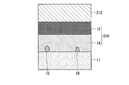
- FIG. 3 is a schematic cross-sectional explanatory view of the bonding layer 18 formed between the ceramic substrate 11 and the circuit layer 12.
- a Cu—Sn layer 14 is formed in the vicinity of the bonding surface of the ceramic substrate 11 in the bonding layer 18 between the ceramic substrate 11 and the circuit layer 12, and the Ti—Sn layer 14 has a Ti— A Ti-containing layer 15 containing is formed.
- the Cu—Sn layer 14 is a layer in which Sn is dissolved in Cu.
- the Cu—Sn layer 14 is a layer formed when P contained in the Cu—P brazing material 24 reacts with Ti of the Ti material 25 and is consumed.
- Examples of the Ti-containing layer 15 include a P—Ti intermetallic compound layer, a Ti layer, and a Cu—Ti intermetallic compound layer. The configuration of the Ti-containing layer 15 varies depending on the amount of Ti in the Ti material 25, bonding conditions, and the like.
- a Cu 3 P phase 16 is dispersed in the Cu—Sn layer 14, and this Cu 3 P phase 16 does not react with Ti of the Ti material 25 and remains in the Cu—P-based brazing material 24.
- P is produced by reacting with Cu.
- the semiconductor element 3 is made of a semiconductor material such as Si.
- the semiconductor element 3 and the circuit layer 12 are joined via the solder layer 2.
- the solder layer 2 is made of, for example, a Sn—Ag, Sn—In, or Sn—Ag—Cu solder material.
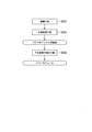
- a Cu—P brazing material 24, a Ti material 25, and a Cu plate 22 to be the circuit layer 12 are sequentially laminated on one surface of the ceramic substrate 11 (the upper surface in FIG. 5) ( Lamination process S01).
- this stacking step S01 Cu and Cu are interposed so that the atomic ratio [Ti / P] of P and Ti interposed between the ceramic substrate 11 and the Cu plate 22 is in the range of 0.1 to 0.8.
- -P-type brazing material 24 and Ti material 25 are arranged.
- the atomic ratio [Ti / P] of P and Ti interposed between the ceramic substrate 11 and the Cu plate 22 is less than 0.1, the amount of Ti that reacts with P becomes insufficient, and Cu A large amount of 3 P phase 16 is formed, and there is a possibility that the area ratio of the Cu 3 P phase in the region from the bonding surface of the ceramic substrate 11 to the circuit layer 12 side up to 50 ⁇ m cannot be made 15% or less.
- the atomic ratio [Ti / P] of P and Ti interposed between the ceramic substrate 11 and the Cu plate 22 exceeds 0.8, the liquid phase of the brazing material generated when heated is Ti Therefore, the melting point of the liquid phase rises and solidification easily proceeds.
- the atomic ratio [Ti / P] of P and Ti interposed between the ceramic substrate 11 and the Cu plate 22 is in the range of 0.1 to 0.8. It is set.
- the lower limit of the atomic ratio [Ti / P] of P and Ti interposed between the ceramic substrate 11 and the Cu plate 22 is 0.15 or more. It is preferable to set it to 0.2 or more.
- the upper limit of the atomic ratio [Ti / P] of P and Ti interposed between the ceramic substrate 11 and the Cu plate 22 is set to 0.7 or less. It is preferable to set it to 0.6 or less.
- the Ti material 25 is preferably formed by vapor deposition or sputtering when the thickness is from 0.1 ⁇ m to less than 1 ⁇ m, and a foil material is preferably used when the thickness is from 1 ⁇ m to 5 ⁇ m.
- the lower limit of the thickness of the Ti material 25 is preferably 0.2 ⁇ m or more, and more preferably 0.4 ⁇ m or more.
- the upper limit of the thickness of the Ti material 25 is preferably 3 ⁇ m or less, and more preferably 1.5 ⁇ m or less.
- the pressure in the vacuum heating furnace is in the range of 10 ⁇ 6 Pa to 10 ⁇ 3 Pa
- the heating temperature is in the range of 600 ° C. to 650 ° C.
- the heating time is 30 minutes or more. It is set within the range of 240 minutes or less.
- the rate of temperature increase up to the above heating temperature is in the range of 5 ° C./min to 30 ° C./min.
- the rate of temperature rise to the above heating temperature is set within a range of 5 ° C./min to 30 ° C./min.
- the lower limit of the heating rate up to the heating temperature is preferably 7 ° C./min or more, and more preferably 10 ° C./min or more. preferable.
- the upper limit of the heating rate to the heating temperature described above and below 25 ° C. / min further be 20 ° C. / min or less preferable.
- the Cu—P brazing material 24 is melted to form a liquid phase, the Ti material 25 is dissolved in the liquid phase, and the liquid phase is solidified. And are joined. At this time, P contained in the Cu—P brazing material 24 is bonded to Ti of the Ti material 25, and the Cu—Sn layer 14 is formed on the bonding surface side of the ceramic substrate 11. As a result, the circuit layer 12 is formed on one surface of the ceramic substrate 11, and the power module substrate 10 according to this embodiment is manufactured.
- the semiconductor element 3 is bonded to the upper surface of the circuit layer 12 of the power module substrate 10 via a solder material (semiconductor element bonding step S03). In this way, the power module 1 according to this embodiment is manufactured.
- the circuit layer extends from the bonding surface of the ceramic substrate 11. Since the area ratio of the Cu 3 P phase 16 in the region up to 50 ⁇ m toward the 12 side is set to 15% or less, the area occupied by the brittle Cu 3 P phase 16 in the bonding layer 18 is small. Even when a cooling cycle that reaches a high temperature is applied, the occurrence of partial discharge due to the Cu 3 P phase 16 on the circuit layer 12 side can be suppressed. Therefore, the power module substrate 10 according to the present embodiment is excellent in reliability when used in a high temperature environment.
- the ceramic substrate 11 and the Cu plate 22 are laminated in the laminating step S01 in which the ceramic substrate 11 and the Cu plate 22 that becomes the circuit layer 12 are laminated via the Cu—P brazing material 24 and the Ti material 25.
- the Cu—P brazing material 24 and the Ti material 25 are arranged so that the atomic ratio [Ti / P] of P and Ti intervening in between is 0.1 to 0.8. Therefore, the amount of Ti that reacts with P is secured, and unreacted P is reduced, so that formation of the Cu 3 P phase 16 can be suppressed. Therefore, the occurrence of partial discharge can be suppressed.
- the temperature increase rate to the heating temperature in the heat treatment step S02 is set to 5 ° C./min or more and 30 ° C./min or less, formation of the Cu 3 P phase 16 can be suppressed. Therefore, the occurrence of partial discharge can be suppressed.
- the pressure applied is 1 kgf / cm 2 or more, so that the liquid phase of the ceramic substrate 11 and the Cu—P brazing material 24 can be brought into close contact, and the ceramic substrate 11 and the Cu— -The Sn layer 14 can be bonded well. Moreover, since the pressurized pressure is set to 35 kgf / cm 2 or less, the occurrence of cracks in the ceramic substrate 11 can be suppressed.
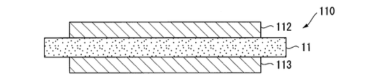
- FIG. 6 shows a power module 101 including the power module substrate 110 according to the second embodiment.
- the power module 101 includes a power module substrate 110 on which a circuit layer 112 and a metal layer 113 are disposed, and a semiconductor element bonded to one surface (upper surface in FIG. 6) of the circuit layer 112 via a solder layer 2. 3 and a heat sink 130 disposed on the other side of the metal layer 113 (lower side in FIG. 6).
- the power module substrate 110 includes a ceramic substrate 11, a circuit layer 112 disposed on one surface of the ceramic substrate 11 (upper surface in FIG. 7), and the other surface of the ceramic substrate 11. And a metal layer 113 disposed on the lower surface in FIG.
- the ceramic substrate 11 is made of AlN (aluminum nitride) with excellent heat dissipation.
- the circuit layer 112 is formed by sequentially laminating a Cu—P brazing material 124, a Ti material 25, and a Cu plate 122 made of oxygen-free copper on one surface of the ceramic substrate 11, and heat-treating them. It is formed by bonding a Cu plate 122 to the ceramic substrate 11 (see FIG. 10). Note that the thickness of the circuit layer 112 is set within a range of 0.1 mm or more and 1.0 mm or less, and is set to 0.2 mm in the present embodiment.
- the metal layer 113 is formed by bonding a Cu or Cu alloy metal plate to the other surface of the ceramic substrate 11 via a Cu—P brazing material 124.
- the metal layer 113 is formed by laminating a Cu-P brazing material 124, a Ti material 25, and a Cu plate 123 made of oxygen-free copper on the other surface of the ceramic substrate 11, and heat-treating it. It is formed by bonding a Cu plate 123 (see FIG. 10).
- the thickness of the metal layer 113 is set within a range of 0.1 mm or more and 1.0 mm or less, and is set to 0.15 mm in the present embodiment.
- a Cu—P—Sn—Ni brazing material is specifically used as the Cu—P brazing material 124.
- FIG. 8 is a schematic cross-sectional explanatory view of the bonding layer 118 between the ceramic substrate 11 and the circuit layer 112 and the metal layer 113.
- a Cu—Sn layer 14 is formed in the vicinity of the bonding surface of the ceramic substrate 11, and the circuit layer 112 side of this Cu—Sn layer 14 is formed.
- a Ti-containing layer 15 containing Ti is formed on the metal layer 113 side.
- the Cu 3 P phase 16 is dispersed in the Cu—Sn layer 14. In this Cu 3 P phase 16, the remaining P reacts with Cu without reacting with Ti of the Ti material 25. Generated by.
- the bonding surface of the ceramic substrate 11 is up to 50 ⁇ m from the bonding surface to the circuit layer 112 and the metal layer 113 side.
- the area ratio of the Cu 3 P phase in the region is 15% or less.
- the heat sink 130 dissipates heat from the power module substrate 110 described above.
- the heat sink 130 is made of Cu or Cu alloy, and in this embodiment is made of oxygen-free copper.
- the heat sink 130 is provided with a flow path 131 through which a cooling fluid flows.
- the heat sink 130 and the metal layer 113 are joined by a solder layer 132 made of a solder material.
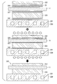
- a Cu—P brazing material 124, a Ti material 25, and a Cu plate 122 to be the circuit layer 112 are sequentially laminated on one surface (the upper surface in FIG. 10) of the ceramic substrate 11.
- the Cu—P brazing material 124, the Ti material 25, and the Cu plate 123 to be the metal layer 113 are sequentially laminated on the other surface (the lower surface in FIG. 10) of the ceramic substrate 11 (lamination step S101).
- the atomic ratio [Ti / P] of P and Ti interposed between the ceramic substrate 11 and the Cu plates 122 and 123 is in the range of 0.1 to 0.8.
- the Cu—P brazing material 124 and the Ti material 25 are disposed. Specifically, in consideration of the P content of the Cu—P brazing material 124 and the purity of the Ti material 25, by adjusting the thickness of the Cu—P brazing material 124 and the thickness of the Ti material 25, The atomic ratio [Ti / P] of P and Ti interposed between the ceramic substrate 11 and the Cu plate 22 is adjusted.
- the Cu plate 122, the Ti material 25, the Cu—P based brazing material 124, the ceramic substrate 11, the Cu—P based brazing material 124, the Ti material 25, and the Cu plate 123 are pressurized (pressure 1 kgf / In a state where it is not lower than cm 2 and not higher than 35 kgf / cm 2, it is placed in a vacuum heating furnace and heated to a temperature equal to or higher than the melting start temperature of the Cu—P brazing filler metal 124 (heat treatment step S102).
- the rate of temperature rise up to the above heating temperature is in the range of 5 ° C./min to 30 ° C./min.
- the Cu—P brazing material 124 melts to form a liquid phase, the Ti material 25 dissolves in this liquid phase, and the liquid phase solidifies, whereby the ceramic substrate 11 and the Cu plate 122 The ceramic substrate 11 and the Cu plate 123 are joined. At this time, P contained in the Cu—P based brazing material 124 is bonded to Ti of the Ti material 25, and the Cu—Sn layer 14 is formed on the ceramic substrate 11 side.
- the circuit layer 112 is formed on one surface of the ceramic substrate 11 and the metal layer 113 is formed on the other surface, and the power module substrate 110 according to this embodiment is manufactured.
- the heat sink 130 is bonded to the lower surface of the metal layer 113 of the power module substrate 110 via a solder material (heat sink bonding step S103).
- the semiconductor element 3 is bonded to the upper surface of the circuit layer 112 of the power module substrate 110 via a solder material (semiconductor element bonding step S104). In this way, the power module 101 according to this embodiment is manufactured.
- the ceramics in the bonding interface between the ceramic substrate 11 and the circuit layer 112 and in the bonding layer 118 between the ceramic substrate 11 and the metal layer 113 Since the area ratio of the Cu 3 P phase 16 in the region from the bonding surface of the substrate 11 to the circuit layer 112 side and the metal layer 113 side to 50 ⁇ m is 15% or less, the brittle Cu 3 P phase 16 in the bonding layer 118 is obtained. Even when a cooling cycle that reaches a relatively high temperature such as 200 ° C. or higher is loaded, the occurrence of partial discharge can be suppressed.
- the circuit layer 112 is bonded to one surface of the ceramic substrate 11 and the metal layer 113 is bonded to the other surface at the same time.
- the manufacturing process can be simplified and the manufacturing cost can be reduced.
- FIG. 11 shows a power module 201 including a power module substrate 210 according to the third embodiment.
- This power module 201 includes a power module substrate 210 on which a circuit layer 212 and a metal layer 213 are disposed, and a semiconductor element bonded to one surface (upper surface in FIG. 11) of the circuit layer 212 via a solder layer 2. 3 and a heat sink 230 bonded to the other side (lower side in FIG. 11) of the power module substrate 210.
- the power module substrate 210 includes a ceramic substrate 11, a circuit layer 212 disposed on one surface (the upper surface in FIG. 12) of the ceramic substrate 11, and the other surface of the ceramic substrate 11. And a metal layer 213 disposed on the lower surface in FIG.
- the ceramic substrate 11 is made of AlN (aluminum nitride) having excellent heat dissipation.
- the circuit layer 212 is obtained by laminating a Cu-P brazing material 224, a Ti material 25, and a Cu plate 222 made of oxygen-free copper on one surface of the ceramic substrate 11, and heat-treating the ceramic layer. It is formed by bonding a Cu plate 222 to the substrate 11 (see FIG. 15).
- the thickness of the circuit layer 212 is set within a range of 0.1 mm or more and 1.0 mm or less, and is set to 0.2 mm in the present embodiment.
- a Cu—P—Sn—Ni brazing material is specifically used as the Cu—P brazing material 224.
- FIG. 13 is a schematic cross-sectional explanatory view of the bonding layer 218 between the ceramic substrate 11 and the circuit layer 212.
- a Cu—Sn layer 14 is formed in the vicinity of the bonding surface of the ceramic substrate 11 in the bonding layer 218 between the ceramic substrate 11 and the circuit layer 212, and the Ti—Sn layer 14 has a Ti— A Ti-containing layer 15 containing is formed.
- the Cu 3 P phase 16 is dispersed in the Cu—Sn layer 14.
- the Cu 3 P phase 16 is generated by reacting P remaining without reacting with Ti of the Ti material 25 with Cu.
- the Cu 3 P phase 16 in the bonding layer 218 formed between the ceramic substrate 11 and the circuit layer 212 in the bonding layer 218 formed between the ceramic substrate 11 and the circuit layer 212, the Cu 3 P phase 16 in the region from the bonding surface of the ceramic substrate 11 to the circuit layer 212 side up to 50 ⁇ m.
- the area ratio is 15% or less.
- the metal layer 213 is formed by bonding an Al plate made of Al or an Al alloy to the other surface of the ceramic substrate 11.
- the metal layer 213 is formed by bonding an Al plate 223 having a purity of 99.99 mass% or more to the other surface of the ceramic substrate 11 (see FIG. 15).
- the Al plate 223 is bonded using a bonding material 227 made of an Al—Si brazing material.
- the thickness of the metal layer 213 is set within a range of 0.1 mm to 3.0 mm, and is set to 2.1 mm in the present embodiment.
- the heat sink 230 is made of Al or an Al alloy, and is made of A6063 (Al alloy) in the present embodiment.
- the heat sink 230 is provided with a flow path 231 through which a cooling fluid flows.
- the heat sink 230 and the metal layer 213 are bonded together by a bonding material 242 made of an Al—Si brazing material.
- a method for manufacturing the power module 201 according to the present embodiment will be described with reference to the flowchart of FIG. 14 and FIG.
- a Cu—P brazing material 224, a Ti material 25, and a Cu plate 222 to be a circuit layer 212 are sequentially laminated on one surface (the upper surface in FIG. 15) of the ceramic substrate 11.
- an Al plate 223 to be the metal layer 213 is sequentially laminated on the other surface (the lower surface in FIG. 15) of the ceramic substrate 11 with a bonding material 227 interposed therebetween.
- a heat sink 230 is laminated below the Al plate 223 via the bonding material 242 (lamination step S201).
- the Cu and Ti atomic ratio [Ti / P] interposed between the ceramic substrate 11 and the Cu plate 222 is within a range of 0.1 to 0.8.
- a P-type brazing material 224 and a Ti material 25 are disposed. Specifically, in consideration of the P content of the Cu—P brazing material 224 and the purity of the Ti material 25, by adjusting the thickness of the Cu—P brazing material 224 and the thickness of the Ti material 25, The atomic ratio [Ti / P] of P and Ti interposed between the ceramic substrate 11 and the Cu plate 222 is adjusted.
- the ceramic substrate 11, the Cu—P brazing material 224, the Ti material 25 and the Cu plate 222, the bonding material 227, the Al plate 223, the bonding material 242, and the heat sink 230 are pressurized in the stacking direction (pressure 1 to 35 kgf / pressure). cm 2 ), it is charged into a vacuum heating furnace and heated (heat treatment step S202).
- the pressure in the vacuum heating furnace is in the range of 10 ⁇ 6 Pa to 10 ⁇ 3 Pa
- the heating temperature is in the range of 600 ° C. to 650 ° C.
- the heating time is 30 minutes or more. It is set within the range of 240 minutes or less.
- the rate of temperature increase up to the above heating temperature is in the range of 5 ° C./min to 30 ° C./min.
- the Cu—P brazing material 224 is melted to form a liquid phase, the Ti material 25 is dissolved in the liquid phase, and the liquid phase is solidified, whereby the ceramic substrate 11 and the Cu plate 222 are formed. Are joined. At this time, P contained in the Cu—P based brazing material 224 is bonded to Ti of the Ti material 25, and the Cu—Sn layer 14 is formed on the ceramic substrate 11 side.
- the bonding material 227 is melted to form a liquid phase, and the liquid phase is solidified, whereby the ceramic substrate 11 and the Al plate 223 are bonded via the bonding material 227.
- the bonding material 242 is melted to form a liquid phase, and the liquid phase is solidified, whereby the Al plate 223 and the heat sink 230 are bonded via the bonding material 242.
- the power module substrate 210 and the power module substrate with a heat sink according to the present embodiment are manufactured.
- the semiconductor element 3 is bonded to the upper surface of the circuit layer 212 of the power module substrate 210 via a solder material (semiconductor element bonding step S203). In this way, the power module 201 according to this embodiment is manufactured.
- the power module substrate 210 according to the present embodiment configured as described above has the same effects as the power module substrate 10 described in the first embodiment. Further, in the power module substrate 210 according to the present embodiment, the metal layer 213 formed by bonding the Al plate 223 to the other surface of the ceramic substrate 11 is formed. It can be efficiently dissipated through the layer 213. Further, since Al has a relatively low deformation resistance, the thermal stress generated between the power module substrate 210 and the heat sink 230 is absorbed by the metal layer 213 when a cooling cycle is applied, and the ceramic substrate 11 is not cracked. Occurrence can be suppressed.
- the ceramic substrate 11 and the Cu plate 222 can be bonded at a relatively low temperature.
- the metal layer 213 made of the plate 223 can be bonded at the same time, so that the manufacturing process can be simplified and the manufacturing cost can be reduced.
- the power module is configured by mounting a semiconductor element on an insulating circuit board.
- the present invention is not limited to this.
- an LED module may be configured by mounting LED elements on a circuit layer of an insulated circuit board, or a thermoelectric module may be configured by mounting thermoelectric elements on a circuit layer of an insulated circuit board.
- the case where the circuit layer is bonded to one surface of the ceramic substrate and the metal layer is simultaneously bonded to the other surface has been described. However, the circuit layer and the metal layer are separately provided. You may join.
- the case where the circuit layer, the metal layer, and the heat sink are simultaneously bonded has been described. However, the circuit layer and the metal layer may be bonded to the ceramic substrate, and then the metal layer and the heat sink may be bonded. good.
- the case where the metal layer is bonded to the other surface of the ceramic substrate via the Al—Si brazing material has been described, but the bonding is performed by a transient liquid phase bonding method (TLP), Ag paste, or the like. May be.
- TLP transient liquid phase bonding method
- the heat sink provided with the flow path has been described in the second embodiment and the third embodiment, a plate-like thing called a heat radiating plate or a pin-like fin may be used.
- the power module substrate and the heat sink may be fixed by screwing or the like via grease.
- the heat sink may not be bonded to the other surface side of the power module substrate.
- a Ti foil may be used, or the Ti material may be formed by vapor deposition or sputtering.
- a Cu member / Ti clad material in which Ti is disposed on one surface of the Cu member can be used.
- a Ti material / brazing material clad material in which a Cu—P brazing material is disposed on one surface of the Ti material, and a Cu member / Ti material laminated in the order of a Cu member, a Ti material, and a Cu—P based brazing material. / Brazer cladding can be used.
- the Cu—P brazing material has been described as using a Cu—P—Sn—Ni brazing material, but other Cu—P brazing materials such as a Cu—P brazing material may be used. Good.
- a Cu—P brazing material suitable for the method for producing a joined body of the present invention will be described in detail.
- the content of P in the Cu—P brazing material is preferably 3 mass% or more and 10 mass% or less.
- P is an element having an effect of lowering the melting start temperature of the brazing material. Moreover, this P prevents oxidation of the brazing filler metal by covering the surface of the brazing filler metal with the P oxide generated by oxidation of P, and the surface of the molten brazing filler metal has good fluidity. It is an element having an effect of improving the wettability of the brazing material by covering. If the P content is less than 3 mass%, the effect of lowering the melting start temperature of the brazing material cannot be sufficiently obtained, the melting start temperature of the brazing material is increased, or the fluidity of the brazing material is insufficient.
- the bondability with the layer may decrease.
- the P content exceeds 10 mass%, a large amount of brittle intermetallic compounds are formed, and the bonding properties and bonding reliability between the ceramic substrate and the circuit layer may be reduced.
- the content of P contained in the Cu—P brazing material is preferably in the range of 3 mass% to 10 mass%.
- the Cu—P brazing material may contain Sn in an amount of 0.5 mass% to 25 mass%.
- Sn is an element having an effect of lowering the melting point of the brazing material.
- the Sn content is 0.5 mass% or more, the melting point of the brazing material can be reliably lowered. Further, when the Sn content is 25 mass% or less, the low temperature embrittlement of the brazing material can be suppressed, and the bonding reliability between the ceramic substrate and the circuit layer can be improved.
- the content is preferably in the range of 0.5 mass% to 25 mass%.
- the Cu—P brazing material may contain 2 mass% or more and 20 mass% or less of any one or more of Ni, Cr, Fe, and Mn.
- Ni, Cr, Fe, and Mn are elements having an effect of suppressing the formation of an intermetallic compound containing P at the interface between the ceramic substrate and the brazing material.
- the content of one or more of Ni, Cr, Fe, and Mn is 2 mass% or more, the formation of intermetallic compounds containing P at the bonding interface between the ceramic substrate and the brazing material is suppressed. This improves the bonding reliability between the ceramic substrate and the circuit layer.
- the content of any one or more of Ni, Cr, Fe, and Mn is 20 mass% or less, an increase in the melting start temperature of the brazing material is suppressed, and the fluidity of the brazing material is lowered. This can suppress this and improve the bondability between the ceramic substrate and the circuit layer.
- the content should be in the range of 2 mass% to 20 mass%. Is preferred.
- Example 1 Below, the result of the confirmation experiment (Example 1) conducted in order to confirm the effect of this invention is demonstrated.
- a Cu plate (37 mm ⁇ 37 mm ⁇ 0.2 mmt) made of Cu—P brazing material, Ti material and oxygen-free copper shown in Table 1 Laminate sequentially.
- the Cu—P-based brazing material and the Ti material were arranged so that the atomic ratio [Ti / P] of P and Ti interposed between the ceramic substrate and the Cu plate was the value shown in Table 1.
- the ceramic substrate used in this example was a ceramic substrate of ZrO 2 was added to sinter 10 mass% of AlN as 100 mass%.
- the ceramic substrate is heated by being charged in a vacuum heating furnace in a state of being pressurized at a pressure of 15 kgf / cm 2 in the laminating direction and heated at a temperature equal to or higher than the melting start temperature of the Cu—P brazing filler metal.
- a Cu plate was bonded to one surface to form a circuit layer.
- the heating temperature in this heat treatment step, the holding time at the heating temperature, and the rate of temperature rise to the heating temperature were carried out under the conditions shown in Table 1.
- the area ratio of the Cu 3 P phase in the vicinity of the ceramic substrate and the partial discharge characteristics in the bonding layer between the ceramic substrate and the circuit layer were evaluated.
- the obtained power module substrate was loaded with 100 cycles of a cooling cycle of 5 minutes at 200 ° C. and 5 minutes at ⁇ 40 ° C. Thereafter, a probe is applied to the surface of the circuit layer of the power module substrate and the side of the ceramic substrate where the circuit layer is not formed, immersed in 3M Fluorinert, and the measurement voltage is measured under the conditions specified in the international standard IEC61287. Was set to 3.3 kV, and the partial discharge characteristics were evaluated. Table 1 shows the measurement voltage evaluation results.
- Comparative Example 1-1 the atomic ratio [Ti / P] of P and Ti intervening between the ceramic substrate and the Cu plate is less than 0.1, and up to 50 ⁇ m from the bonding surface of the ceramic substrate to the Cu plate side. Since the area ratio of the Cu 3 P phase in the region exceeded 15%, the partial discharge characteristics were insufficient. In Comparative Example 1-2, the atomic ratio [Ti / P] of P and Ti interposed between the ceramic substrate and the Cu plate exceeded 0.8, and the partial discharge characteristics were insufficient.
- the rate of temperature increase to the heating temperature in the heat treatment step is less than 5 ° C./min, and the area of the Cu 3 P phase in the region from the bonding surface of the ceramic substrate to the Cu plate side to 50 ⁇ m. Since the rate exceeded 15%, the partial discharge characteristics were insufficient. In Comparative Example 1-4, the rate of temperature rise to the heating temperature in the heat treatment process exceeded 30 ° C./min, and the partial discharge characteristics were insufficient.
- Examples 1-1 to 1-8 of the present invention all had excellent partial discharge characteristics. According to Example 1, it was confirmed that partial discharge characteristics can be improved when a Cu plate is bonded to one surface of a ceramic substrate.
- Example 2 Next, the result of a confirmation experiment (Example 2) conducted to confirm the effect of the present invention will be described.
- a Cu plate (37 mm ⁇ 37 mm ⁇ 0) made of Cu—P brazing material, Ti material and oxygen-free copper shown in Table 2 .2 mmt) in order.
- the Cu—P based brazing material and the Ti material were arranged so that the atomic ratio [Ti / P] of P and Ti interposed between the ceramic substrate and the Cu plate was the numerical value shown in Table 2.
- the ceramic substrate used in this example was a ceramic substrate of ZrO 2 was added to sinter 10 mass% of AlN as 100 mass%.
- the ceramic substrate is heated by being charged in a vacuum heating furnace in a state of being pressurized at a pressure of 15 kgf / cm 2 in the laminating direction and heated at a temperature equal to or higher than the melting start temperature of the Cu—P brazing filler metal.
- a Cu plate was bonded to one surface and the other surface to form a circuit layer and a metal layer.
- the heating temperature in this heat treatment step, the holding time at the heating temperature, and the rate of temperature increase up to the heating temperature were carried out under the conditions shown in Table 2.
- Example 2 For the power module substrate obtained as described above, as in Example 1, the area ratio of the Cu 3 P phase in the vicinity of the ceramic substrate in the bonding layer between the ceramic substrate and the circuit layer, and the portion The discharge characteristics were evaluated. In evaluating the partial discharge characteristics, the probe was applied to the surface of the circuit layer and the metal layer. The evaluation results are shown in Table 2.
- Comparative Example 2-1 the atomic ratio [Ti / P] of P and Ti interposed between the ceramic substrate and the Cu plate is less than 0.1, and the distance from the bonding surface of the ceramic substrate to the Cu plate is up to 50 ⁇ m. Since the area ratio of the Cu 3 P phase in the region exceeded 15%, the partial discharge characteristics were insufficient. In Comparative Example 2-2, the atomic ratio [Ti / P] of P and Ti interposed between the ceramic substrate and the Cu plate exceeded 0.8, and the partial discharge characteristics were insufficient.
- the rate of temperature increase to the heating temperature in the heat treatment step is less than 5 ° C./min, and the area of the Cu 3 P phase in the region from the bonding surface of the ceramic substrate to the Cu plate side to 50 ⁇ m. Since the rate exceeded 15%, the partial discharge characteristics were insufficient. In Comparative Example 2-4, the rate of temperature rise to the heating temperature in the heat treatment process exceeded 30 ° C./min, and the partial discharge characteristics were insufficient.
- Examples 2-1 to 2-8 of the present invention were all excellent in partial discharge characteristics. According to Example 2, it was confirmed that partial discharge characteristics can be improved even when Cu plates are bonded to both surfaces of a ceramic substrate.
- Example 3 Next, the results of a confirmation experiment (Example 3) conducted to confirm the effect of the present invention will be described.
- the Al plate (37 mm ⁇ 37 mm ⁇ 2.1 mmt) made of Al having a purity of 99.99 mass% was laminated on the other surface of the ceramic substrate through an Al—Si brazing filler metal.
- the Cu—P-based brazing material and the Ti material were arranged so that the atomic ratio [Ti / P] of P and Ti interposed between the ceramic substrate and the Cu plate was the value shown in Table 3.
- the ceramic substrate used in this example was a ceramic substrate of ZrO 2 was added to sinter 10 mass% of AlN as 100 mass%.
- the pressure is 15 kgf / cm 2 in the laminating direction and charged in a vacuum heating furnace, the pressure is 10 ⁇ 6 Pa or more and 10 ⁇ 3 Pa or less, and the Cu—P brazing material is melted.
- a Cu plate was bonded to one surface of the ceramic substrate to form a circuit layer, and an Al plate was bonded to the other surface of the ceramic substrate to form a metal layer.
- the heating temperature in this heat treatment process, the holding time at the heating temperature, and the rate of temperature increase up to the heating temperature were carried out under the conditions shown in Table 3.
- Example 2 For the power module substrate obtained as described above, as in Example 1, the area ratio of the Cu 3 P phase in the vicinity of the ceramic substrate in the bonding layer between the ceramic substrate and the circuit layer, and the portion The discharge characteristics were evaluated. In evaluating the partial discharge characteristics, the probe was applied to the surface of the circuit layer and the metal layer. The evaluation results are shown in Table 3.
- Comparative Example 3-1 the atomic ratio [Ti / P] of P and Ti interposed between the ceramic substrate and the Cu plate is less than 0.1, and the distance from the bonding surface of the ceramic substrate to the Cu plate side is 50 ⁇ m. Since the area ratio of the Cu 3 P phase in the region exceeded 15%, the partial discharge characteristics were insufficient. In Comparative Example 3-2, the atomic ratio [Ti / P] of P and Ti interposed between the ceramic substrate and the Cu plate exceeded 0.8, and the partial discharge characteristics were insufficient.
- the rate of temperature increase to the heating temperature in the heat treatment step is less than 5 ° C./min, and the area of the Cu 3 P phase in the region from the bonding surface of the ceramic substrate to the Cu plate side to 50 ⁇ m. Since the rate exceeded 15%, the partial discharge characteristics were insufficient. In Comparative Example 3-4, the rate of temperature increase to the heating temperature in the heat treatment process exceeded 30 ° C./min, and the partial discharge characteristics were insufficient.
- Examples 3-1 to 3-8 of the present invention were all excellent in partial discharge characteristics.
- This Example 3 confirms that partial discharge characteristics can be improved even when a Cu plate is bonded to one surface of a ceramic substrate and an Al plate is bonded to the other surface of the ceramic substrate. It was.
- Example 4 Next, the results of a confirmation experiment (Example 4) conducted to confirm the effect of the present invention will be described.
- a ceramic substrate made of AlN 40 mm ⁇ 40 mm ⁇ 1.0 mmt
- a Cu plate 37 mm ⁇ 37 mm ⁇ 0
- the Cu—P-based brazing material and the Ti material were arranged so that the atomic ratio [Ti / P] of P and Ti interposed between the ceramic substrate and the Cu plate was the value shown in Table 4.
- the ceramic substrate used in this example was a ceramic substrate of ZrO 2 was added to sinter 10 mass% of AlN as 100 mass%.
- the ceramic substrate is heated by being charged in a vacuum heating furnace in a state of being pressurized at a pressure of 15 kgf / cm 2 in the laminating direction and heated at a temperature equal to or higher than the melting start temperature of the Cu—P brazing filler metal.
- a Cu plate was bonded to one surface and the other surface to form a circuit layer and a metal layer.
- the heating temperature in this heat treatment process, the holding time at the heating temperature, and the rate of temperature increase up to the heating temperature were carried out under the conditions shown in Table 4.
- the area ratio of the Cu 3 P phase in the vicinity of the ceramic substrate in the bonding layer between the ceramic substrate and the circuit layer was evaluated in the same manner as in Example 1.
- partial discharge characteristics first, 200 cycles of a cooling cycle of 15 minutes at 150 ° C. and 15 minutes at ⁇ 50 ° C. were loaded on the obtained power module substrate. After that, the probe is applied to the circuit layer surface and the metal layer surface of the power module substrate, immersed in Fluorinert, the discharge charge amount is set to 5.1 kV under the conditions specified in the international standard IEC61287, The discharge characteristics were evaluated. That is, in Example 4, the partial discharge characteristics at the time of high voltage load were evaluated. The evaluation results are shown in Table 4.
- Comparative Example 4-1 the atomic ratio [Ti / P] of P and Ti interposed between the ceramic substrate and the Cu plate is less than 0.1, and the distance from the bonding surface of the ceramic substrate to the Cu plate is up to 50 ⁇ m. Since the area ratio of the Cu 3 P phase in the region exceeded 15%, the partial discharge characteristics were insufficient. In Comparative Example 4-2, the atomic ratio [Ti / P] of P and Ti interposed between the ceramic substrate and the Cu plate exceeded 0.8, and the partial discharge characteristics were insufficient.
- the rate of temperature increase to the heating temperature in the heat treatment step is less than 5 ° C./min, and the area of the Cu 3 P phase in the region from the bonding surface of the ceramic substrate to the Cu plate side to 50 ⁇ m. Since the rate exceeded 15%, the partial discharge characteristics were insufficient. In Comparative Example 4-4, the rate of temperature rise to the heating temperature in the heat treatment process exceeded 30 ° C./min, and the partial discharge characteristics were insufficient.
- Examples 4-1 to 4-8 of the present invention were all excellent in partial discharge characteristics. According to Example 4, it was confirmed that sufficient partial discharge characteristics could be obtained even when the measurement voltage was set as high as 5.1 Kv.
- Example 5 Next, the results of a confirmation experiment (Example 5) conducted to confirm the effect of the present invention will be described.
- a Cu plate made of Cu—P brazing material, Ti material and oxygen-free copper shown in Table 5 37 mm ⁇ 37 mm ⁇ 0.2 mmt.
- the Cu—P-based brazing material and the Ti material were arranged so that the atomic ratio [Ti / P] of P and Ti interposed between the ceramic substrate and the Cu plate was the value shown in Table 5. .
- the ceramic substrate is heated by being charged in a vacuum heating furnace in a state of being pressurized at a pressure of 15 kgf / cm 2 in the laminating direction and heated at a temperature equal to or higher than the melting start temperature of the Cu—P brazing filler metal.
- a Cu plate was bonded to one surface and the other surface to form a circuit layer and a metal layer.
- the heating temperature in this heat treatment process, the holding time at the heating temperature, and the rate of temperature increase up to the heating temperature were carried out under the conditions shown in Table 5.
- Example 2 For the power module substrate obtained as described above, as in Example 1, the area ratio of the Cu 3 P phase in the vicinity of the ceramic substrate in the bonding layer between the ceramic substrate and the circuit layer, and the portion The discharge characteristics were evaluated. In evaluating the partial discharge characteristics, the probe was applied to the surface of the circuit layer and the metal layer. The evaluation results are shown in Table 5.
- Comparative Example 5-1 the atomic ratio [Ti / P] of P and Ti interposed between the ceramic substrate and the Cu plate is less than 0.1, and the distance from the bonding surface of the ceramic substrate to the Cu plate side is up to 50 ⁇ m. Since the area ratio of the Cu 3 P phase in the region exceeded 15%, the partial discharge characteristics were insufficient. In Comparative Example 5-2, the atomic ratio [Ti / P] of P and Ti interposed between the ceramic substrate and the Cu plate exceeded 0.8, and the partial discharge characteristics were insufficient.
- the rate of temperature rise to the heating temperature in the heat treatment step is less than 5 ° C./min, and the area of the Cu 3 P phase in the region from the bonding surface of the ceramic substrate to the Cu plate side to 50 ⁇ m. Since the rate exceeded 15%, the partial discharge characteristics were insufficient. In Comparative Example 5-4, the rate of temperature rise to the heating temperature in the heat treatment process exceeded 30 ° C./min, and the partial discharge characteristics were insufficient.
- Examples 5-1 to 5-8 of the present invention were all excellent in partial discharge characteristics. According to Example 5, it was confirmed that partial discharge characteristics can be improved even when Cu plates are bonded to both surfaces of a ceramic substrate made of Si 3 N 4 .
- the power module substrate comprising the joined body, the power module, the method for producing the joined body, and the method for producing the power module substrate, the ceramic member and the Cu member are satisfactorily joined.
- a cooling cycle that reaches a relatively high temperature is loaded, it is possible to suppress the occurrence of partial discharge.
Abstract
Description
本願は、2016年1月22日に、日本に出願された特願2016-010676号、及び2017年1月5日に、日本に出願された特願2017-000417号に基づき優先権を主張し、その内容をここに援用する。
風力発電、電気自動車等の電気車両などを制御するために用いられる大電力制御用のパワー半導体素子においては、発熱量が多いことから、これを搭載する基板としては、例えばAlN(窒化アルミニウム)などからなるセラミックス基板の一方の面に導電性の優れた金属板を回路層として接合したパワーモジュール用基板が、従来から広く用いられている。また、セラミックス基板の他方の面に、金属板を金属層として接合することもある。
ところで、特許文献1に開示されたようにCu-Mg-Tiろう材を介してセラミックス基板とCu板とを接合すると、セラミックス基板の近傍には、Cu、Mg、又はTiを含む金属間化合物が形成される。
また、セラミックス基板と回路層を接合する際に、セラミックス基板の近傍に硬い金属間化合物が形成されると、セラミックス基板と回路層との接合率が低下し、良好に接合することができないおそれがあった。
これら特許文献2-4に記載された発明においては、Cu-P系ろう材中のPが活性元素と反応することにより、セラミックス基板側にCu層が形成され、セラミックス基板の近傍に硬い金属間化合物層が配設されない。これにより、冷熱サイクルを負荷した際にセラミックス基板に生じる熱応力を低減でき、セラミックス基板にクラックが発生することを抑制することが可能となる。
ここで、特許文献2-4に記載されたように、Cu-P系ろう材を用いてセラミックス基板とCu板とを接合したパワーモジュール用基板においては、高温にまで達する冷熱サイクルが負荷された際に、部分放電が発生しやすくなるといった問題があった。
この場合、セラミックス基板の他方の面に、比較的変形抵抗の小さなAl又はAl合金からなる金属層が形成されているので、パワーモジュール用基板に応力が負荷された場合に金属層が優先的に変形し、セラミックス基板に作用する応力を低減することができ、セラミックス基板の割れを抑制することができる。
この構成のパワーモジュールによれば、部分放電の発生が抑制されたパワーモジュール用基板を備えているので、比較的高温にまで達する冷熱サイクルが負荷される使用環境下においても信頼性に優れている。
また、比較的低温でCu又はCu合金からなる回路層とセラミックス基板とを接合できるので、Cu又はCu合金からなる回路層と、セラミックス基板と、Al又はAl合金からなる金属層と、を同時に接合することも可能となる。
以下に、本発明の実施形態について添付した図面を参照して説明する。まず、本発明の第一実施形態について説明する。
本実施形態に係る接合体は、セラミックス部材であるセラミックス基板11と、Cu部材であるCu板22(回路層12)とが接合されてなるパワーモジュール用基板10である。図1に、本実施形態であるパワーモジュール用基板10を備えたパワーモジュール1を示す。
このパワーモジュール1は、回路層12が配設されたパワーモジュール用基板10と、回路層12の一方の面(図1において上面)にはんだ層2を介して接合された半導体素子3とを備えている。
セラミックス基板11は、絶縁性の高いAlN(窒化アルミニウム)、Si3N4(窒化ケイ素)、Al2O3(アルミナ)等のセラミックスで構成されている。本実施形態では、放熱性の優れたAlN(窒化アルミニウム)で構成されている。また、セラミックス基板11の厚さは、0.2~1.5mmの範囲内に設定されており、本実施形態では、0.635mmに設定されている。
本実施形態において、回路層12は、セラミックス基板11の一方の面にCu-P系ろう材24、Ti材25、無酸素銅からなるCu板22を積層して加熱処理し、セラミックス基板11にCu板22を接合することで形成されている(図5参照)。なお、本実施形態では、Cu-P系ろう材24として、Cu-P-Sn-Niろう材を用いている。
ここで、回路層12においてセラミックス基板11側は、SnがCu中に固溶した構造となっている。
なお、回路層12の厚さは0.1mm以上1.0mm以下の範囲内に設定されており、本実施形態では、0.2mmに設定されている。
セラミックス基板11と回路層12との間の接合層18のうちセラミックス基板11の接合面近傍にCu-Sn層14が形成されており、このCu-Sn層14の回路層12側には、Tiを含むTi含有層15が形成されている。
Ti含有層15としては、例えば、P-Ti系金属間化合物層、Ti層、Cu-Ti金属間化合物層等が挙げられる。なお、Ti材25におけるTi量や接合条件等により、Ti含有層15の構成は異なる。
そして、本実施形態においては、セラミックス基板11と回路層12との間に形成された接合層18において、セラミックス基板11の接合面から回路層12側へ50μmまでの領域におけるCu3P相の面積率が15%以下とされている。
はんだ層2は、例えばSn-Ag系、Sn-In系、若しくはSn-Ag-Cu系のはんだ材とされている。
この積層工程S01においては、セラミックス基板11とCu板22との間に介在されるPとTiの原子比〔Ti/P〕が0.1以上0.8以下の範囲内となるように、Cu-P系ろう材24及びTi材25を配置する。具体的には、Cu-P系ろう材24のPの含有量及びTi材25の純度を考慮して、Cu-P系ろう材24の厚さとTi材25の厚さを調整することで、セラミックス基板11とCu板22との間に介在されるPとTiの原子比〔Ti/P〕を調整する。
一方、セラミックス基板11とCu板22との間に介在されるPとTiの原子比〔Ti/P〕が0.8を超える場合には、加熱した際に生成するろう材の液相にTiが多く溶け込むため、液相の融点が上昇し凝固が進みやすくなる。その結果、Tiと未反応のPが残留することとなり、Cu3P相16が多く形成する。
そこで、本実施形態では、積層工程S01において、セラミックス基板11とCu板22との間に介在されるPとTiの原子比〔Ti/P〕を0.1以上0.8以下の範囲内に設定している。
また、Cu3P相16の生成をさらに抑制するためには、セラミックス基板11とCu板22との間に介在されるPとTiの原子比〔Ti/P〕の上限を0.7以下とすることが好ましく、0.6以下とすることがさらに好ましい。
この加熱処理工程S02においては、上述の加熱温度までの昇温速度を5℃/min以上30℃/min以下の範囲内としている。
一方、上述の加熱温度までの昇温速度が30℃/minを超える場合には、Tiのろう材の液相への拡散が速くなることから、液相の凝固も早くなり、未反応のPが多く残留し、Cu3P相16が多く形成される。
そこで、本実施形態では、上述の加熱温度までの昇温速度を5℃/min以上30℃/min以下の範囲内に設定している。
また、Cu3P相16の生成をさらに抑制するためには、上述の加熱温度までの昇温速度の上限を25℃/min以下とすることが好ましく、20℃/min以下とすることがさらに好ましい。
これにより、セラミックス基板11の一方の面に回路層12が形成され、本実施形態であるパワーモジュール用基板10が製造される。
このようにして、本実施形態に係るパワーモジュール1が製造される。
次に、本発明の第二実施形態について説明する。なお、第一実施形態と同一の構成のものについては、同一の符号を付して記載し、詳細な説明を省略する。
図6に、第二実施形態に係るパワーモジュール用基板110を備えたパワーモジュール101を示す。
このパワーモジュール101は、回路層112及び金属層113が配設されたパワーモジュール用基板110と、回路層112の一方の面(図6において上面)にはんだ層2を介して接合された半導体素子3と、金属層113の他方側(図6において下側)に配置されたヒートシンク130と、を備えている。
セラミックス基板11は、第一実施形態と同様に、放熱性の優れたAlN(窒化アルミニウム)で構成されている。
なお、回路層112の厚さは0.1mm以上1.0mm以下の範囲内に設定されており、本実施形態では、0.2mmに設定されている。
この金属層113の厚さは0.1mm以上1.0mm以下の範囲内に設定されており、本実施形態では、0.15mmに設定されている。
ここで、本実施形態では、Cu-P系ろう材124として、具体的にはCu-P-Sn―Niろう材を用いている。
セラミックス基板11と回路層112及び金属層113との間の接合層118のうちセラミックス基板11の接合面近傍にCu-Sn層14が形成されており、このCu-Sn層14の回路層112側及び金属層113側には、Tiを含むTi含有層15が形成されている。
そして、本実施形態においては、セラミックス基板11と回路層112及び金属層113との間に形成された接合層118において、セラミックス基板11の接合面から回路層112及び金属層113側へ50μmまでの領域におけるCu3P相の面積率が15%以下とされている。
まず、図10に示すように、セラミックス基板11の一方の面(図10において上面)に、Cu-P系ろう材124、Ti材25、及び回路層112となるCu板122を順に積層するとともに、セラミックス基板11の他方の面(図10において下面)に、Cu-P系ろう材124、Ti材25、及び金属層113となるCu板123を順に積層する(積層工程S101)。
この加熱処理工程S102においては、上述の加熱温度までの昇温速度を5℃/min以上30℃/min以下の範囲内としている。
次に、パワーモジュール用基板110の回路層112の上面に、はんだ材を介して半導体素子3を接合する(半導体素子接合工程S104)。
このようにして、本実施形態に係るパワーモジュール101が製造される。
次に、本発明の第三実施形態について説明する。なお、第一実施形態と同一の構成のものについては、同一の符号を付して記載し、詳細な説明を省略する。
図11に、第三実施形態に係るパワーモジュール用基板210を備えたパワーモジュール201を示す。
このパワーモジュール201は、回路層212及び金属層213が配設されたパワーモジュール用基板210と、回路層212の一方の面(図11において上面)にはんだ層2を介して接合された半導体素子3と、パワーモジュール用基板210の他方側(図11において下側)に接合されたヒートシンク230と、を備えている。
セラミックス基板11は、第一実施形態と同様に、放熱性の優れたAlN(窒化アルミ)で構成されている。
なお、回路層212の厚さは0.1mm以上1.0mm以下の範囲内に設定されており、本実施形態では、0.2mmに設定されている。
ここで、本実施形態では、Cu-P系ろう材224として、具体的にはCu-P-Sn―Niろう材を用いている。
セラミックス基板11と回路層212との間の接合層218のうちセラミックス基板11の接合面近傍にCu-Sn層14が形成されており、このCu-Sn層14の回路層212側には、Tiを含むTi含有層15が形成されている。
そして、本実施形態においては、セラミックス基板11と回路層212との間に形成された接合層218において、セラミックス基板11の接合面から回路層212側へ50μmまでの領域におけるCu3P相16の面積率が15%以下とされている。
この金属層213の厚さは0.1mm以上3.0mm以下の範囲内に設定されており、本実施形態では、2.1mmに設定されている。
まず、図15に示すように、セラミックス基板11の一方の面(図15において上面)に、Cu-P系ろう材224、Ti材25、及び回路層212となるCu板222を順に積層するとともに、セラミックス基板11の他方の面(図15において下面)に、接合材227を介して金属層213となるAl板223を順に積層する。そして、さらにAl板223の下側に、接合材242を介してヒートシンク230を積層する(積層工程S201)。
この加熱処理工程S202においては、上述の加熱温度までの昇温速度を5℃/min以上30℃/min以下の範囲内としている。
また、加熱処理工程S202においては、接合材227が溶融して液相を形成し、この液相が凝固することにより、接合材227を介してセラミックス基板11とAl板223とが接合される。さらに、加熱処理工程S202においては、接合材242が溶融して液相を形成し、この液相が凝固することにより、接合材242を介してAl板223とヒートシンク230とが接合される。
これにより、本実施形態であるパワーモジュール用基板210及びヒートシンク付きパワーモジュール用基板が製造される。
このようにして、本実施形態に係るパワーモジュール201が製造される。
また、本実施形態に係るパワーモジュール用基板210においては、セラミックス基板11の他方の面にAl板223が接合されてなる金属層213が形成されているので、半導体素子3からの熱を、金属層213を介して効率的に放散することができる。また、Alは比較的変形抵抗が低いので、冷熱サイクルが負荷された際に、パワーモジュール用基板210とヒートシンク230との間に生じる熱応力を金属層213によって吸収し、セラミックス基板11に割れが発生することを抑制できる。
例えば、本実施形態では、絶縁回路基板に半導体素子を搭載してパワーモジュールを構成するものとして説明したが、これに限定されることはない。例えば、絶縁回路基板の回路層にLED素子を搭載してLEDモジュールを構成してもよいし、絶縁回路基板の回路層に熱電素子を搭載して熱電モジュールを構成してもよい。
また、第三実施形態において、回路層、金属層、及びヒートシンクを同時に接合する場合について説明したが、回路層と金属層をセラミックス基板に接合した後に、金属層とヒートシンクとを接合する構成としても良い。
また、第三実施形態において、セラミックス基板の他方の面にAl-Si系ろう材を介して金属層を接合する場合について説明したが、過渡液相接合法(TLP)やAgペーストなどによって接合しても良い。
また、パワーモジュール用基板とヒートシンクとをはんだ材又はろう材で接合する場合について説明したが、パワーモジュール用基板とヒートシンクとの間にグリースを介してネジ止めなどによって固定する構成とされても良い。
また、第二実施形態及び第三実施形態のパワーモジュール用基板において、パワーモジュール用基板の他方の面側にヒートシンクが接合されていなくても良い。
さらに、Ti材の一方の面にCu-P系ろう材を配設したTi材/ろう材クラッド材や、Cu部材、Ti材、Cu-P系ろう材の順に積層されたCu部材/Ti材/ろう材クラッドを用いることができる。
Pは、ろう材の溶融開始温度を低下させる作用効果を有する元素である。また、このPは、Pが酸化することで発生するP酸化物により、ろう材表面を覆うことでろう材の酸化を防止するとともに、溶融したろう材の表面を流動性の良いP酸化物が覆うことでろう材の濡れ性を向上させる作用効果を有する元素である。
Pの含有量が3mass%未満では、ろう材の溶融開始温度を低下させる効果が十分に得られずろう材の溶融開始温度が上昇したり、ろう材の流動性が不足し、セラミックス基板と回路層との接合性が低下したりするおそれがある。また、Pの含有量が10mass%超では、脆い金属間化合物が多く形成され、セラミックス基板と回路層との接合性や接合信頼性が低下するおそれがある。
このような理由からCu-P系ろう材に含まれるPの含有量は、3mass%以上10mass%以下の範囲内とすることが好ましい。
Snは、ろう材の融点を低下させる作用効果を有する元素である。Snの含有量が0.5mass%以上では、ろう材の融点を確実に低くすることができる。また、Snの含有量が25mass%以下では、ろう材の低温脆化を抑制することができ、セラミックス基板と回路層との接合信頼性を向上させることができる。
このような理由からCu-P系ろう材にSnを含有させる場合、その含有量は0.5mass%以上25mass%以下の範囲内とすることが好ましい。
Ni、Cr、Fe、Mnは、セラミックス基板とろう材との界面にPを含有する金属間化合物が形成されることを抑制する作用効果を有する元素である。
Ni、Cr、Fe、Mnのうちいずれか1種または2種以上の含有量が2mass%以上では、セラミックス基板とろう材との接合界面にPを含有する金属間化合物が形成されることを抑制することができ、セラミックス基板と回路層との接合信頼性が向上する。また、Ni、Cr、Fe、Mnのうちいずれか1種または2種以上の含有量が20mass%以下では、ろう材の溶融開始温度が上昇することを抑制し、ろう材の流動性が低下することを抑え、セラミックス基板と回路層との接合性を向上させることができる。
このような理由からCu-P系ろう材にNi、Cr、Fe、Mnのうちいずれか1種または2種以上を含有させる場合、その含有量は2mass%以上20mass%以下の範囲内とすることが好ましい。
以下に、本発明の効果を確認すべく行った確認実験(実施例1)の結果について説明する。
このとき、セラミックス基板とCu板との間に介在されるPとTiの原子比〔Ti/P〕が表1に記載の数値となるように、Cu-P系ろう材及びTi材を配置した。
なお、本実施例において使用したセラミックス基板は、AlNを100mass%としてZrO2を10mass%添加して焼結したセラミックス基板とした。
この加熱処理工程における加熱温度、加熱温度における保持時間、加熱温度までの昇温速度を表1の条件で実施した。
上述したパワーモジュール用基板のCu板/セラミックス基板界面の断面をEPMA(電子線マイクロアナライザー)を用い、750倍で観察し、セラミックス基板の接合面からCu板側へ50μmの領域Aの面積aを求めた。次に、領域A内において、P濃度が22at%~28at%の領域BをCu3P相とみなし、その面積bを求め、面積b/面積aをCu3P相の面積率(%)とした。評価結果を表1に示す。なお、観察は5視野で行い、Cu3P相の面積率はこの5視野の面積率の平均とした。
得られたパワーモジュール用基板に対し、200℃で5分と-40℃で5分の冷熱サイクルを100サイクル負荷した。その後、パワーモジュール用基板の回路層表面及びセラミックス基板の回路層の形成されていない側にプローブを当て、3M社製フロリナートに浸漬し、放電電荷量を国際規格IEC61287に規定する条件で、測定電圧を3.3kVに設定し、部分放電特性を評価した。測定電圧評価結果を表1に示す。

比較例1-2は、セラミックス基板とCu板の間に介在されるPとTiの原子比〔Ti/P〕が0.8を超えており、部分放電特性が不十分であった。
比較例1-4は、加熱処理工程における加熱温度までの昇温速度が30℃/minを超えており、部分放電特性が不十分であった。
次に、本発明の効果を確認すべく行った確認実験(実施例2)の結果について説明する。
このとき、セラミックス基板とCu板との間に介在されるPとTiの原子比〔Ti/P〕が表2に記載の数値となるように、Cu-P系ろう材及びTi材を配置した。
なお、本実施例において使用したセラミックス基板は、AlNを100mass%としてZrO2を10mass%添加して焼結したセラミックス基板とした。
この加熱処理工程における加熱温度、加熱温度における保持時間、加熱温度までの昇温速度を表2の条件で実施した。
評価結果を表2に示す。

比較例2-2は、セラミックス基板とCu板の間に介在されるPとTiの原子比〔Ti/P〕が0.8を超えており、部分放電特性が不十分であった。
比較例2-4は、加熱処理工程における加熱温度までの昇温速度が30℃/minを超えており、部分放電特性が不十分であった。
次に、本発明の効果を確認すべく行った確認実験(実施例3)の結果について説明する。
このとき、セラミックス基板とCu板との間に介在されるPとTiの原子比〔Ti/P〕が表3に記載の数値となるように、Cu-P系ろう材及びTi材を配置した。
なお、本実施例において使用したセラミックス基板は、AlNを100mass%としてZrO2を10mass%添加して焼結したセラミックス基板とした。
この加熱処理工程における加熱温度、加熱温度における保持時間、加熱温度までの昇温速度を表3の条件で実施した。
評価結果を表3に示す。

比較例3-2は、セラミックス基板とCu板の間に介在されるPとTiの原子比〔Ti/P〕が0.8を超えており、部分放電特性が不十分であった。
比較例3-4は、加熱処理工程における加熱温度までの昇温速度が30℃/minを超えており、部分放電特性が不十分であった。
次に、本発明の効果を確認すべく行った確認実験(実施例4)の結果について説明する。
このとき、セラミックス基板とCu板との間に介在されるPとTiの原子比〔Ti/P〕が表4に記載の数値となるように、Cu-P系ろう材及びTi材を配置した。
なお、本実施例において使用したセラミックス基板は、AlNを100mass%としてZrO2を10mass%添加して焼結したセラミックス基板とした。
この加熱処理工程における加熱温度、加熱温度における保持時間、加熱温度までの昇温速度を表4の条件で実施した。
また、部分放電特性については、まず、得られたパワーモジュール用基板に対し、150℃で15分と-50℃で15分の冷熱サイクルを200サイクルを負荷した。そして、その後、パワーモジュール用基板の回路層表面及び金属層表面にプローブを当て、フロリナートに浸漬し、放電電荷量を国際規格IEC61287に規定する条件で、測定電圧を5.1kVに設定し、部分放電特性を評価した。すなわち、この実施例4においては、高電圧負荷時の部分放電特性について評価した。
評価結果を表4に示す。

比較例4-2は、セラミックス基板とCu板の間に介在されるPとTiの原子比〔Ti/P〕が0.8を超えており、部分放電特性が不十分であった。
比較例4-4は、加熱処理工程における加熱温度までの昇温速度が30℃/minを超えており、部分放電特性が不十分であった。
次に、本発明の効果を確認すべく行った確認実験(実施例5)の結果について説明する。
このとき、セラミックス基板とCu板との間に介在されるPとTiの原子比〔Ti/P〕が表5に記載の数値となるように、Cu-P系ろう材及びTi材を配置した。
この加熱処理工程における加熱温度、加熱温度における保持時間、加熱温度までの昇温速度を表5の条件で実施した。
評価結果を表5に示す。

比較例5-2は、セラミックス基板とCu板の間に介在されるPとTiの原子比〔Ti/P〕が0.8を超えており、部分放電特性が不十分であった。
比較例5-4は、加熱処理工程における加熱温度までの昇温速度が30℃/minを超えており、部分放電特性が不十分であった。
11 セラミックス基板(セラミックス部材)
12、112、212 回路層(Cu部材)
16 Cu3P相
18,118,218 接合層
22、122、123、222 Cu板(Cu部材)
24,124,224 Cu-P系ろう材
113 金属層(Cu部材)
Claims (9)
- セラミックスからなるセラミックス部材とCu又はCu合金からなるCu部材との接合体であって、
前記セラミックス部材と前記Cu部材との間に形成された接合層において、前記セラミックス部材の接合面から前記Cu部材側へ50μmまでの領域におけるCu3P相の面積率が15%以下とされていることを特徴とする接合体。 - 請求項1に記載の接合体からなり、
前記セラミックス部材からなるセラミックス基板と、このセラミックス基板の一方の面に形成された前記Cu部材からなる回路層と、を備え、
前記セラミックス基板と前記回路層との間に形成された接合層において、前記セラミックス基板の接合面から前記回路層側へ50μmまでの領域におけるCu3P相の面積率が15%以下とされていることを特徴とするパワーモジュール用基板。 - 前記セラミックス基板の他方の面に、Al又はAl合金からなる金属層が形成されていることを特徴とする請求項2に記載のパワーモジュール用基板。
- 請求項1に記載の接合体からなり、
前記セラミックス部材からなるセラミックス基板と、このセラミックス基板の一方の面に形成された回路層と、前記セラミックス基板の他方の面に形成された前記Cu部材からなる金属層と、を備え、
前記セラミックス基板と前記金属層との間に形成された接合層において、前記セラミックス基板の接合面から前記金属層側へ50μmまでの領域におけるCu3P相の面積率が15%以下とされていることを特徴とするパワーモジュール用基板。 - 請求項2から請求項4のいずれか一項に記載されたパワーモジュール用基板と、前記パワーモジュール用基板の前記回路層上に搭載された半導体素子と、を備えたことを特徴とするパワーモジュール。
- セラミックスからなるセラミックス部材とCu又はCu合金からなるCu部材との接合体の製造方法であって、
Cu-P系ろう材とTi材とを介して前記セラミックス部材と前記Cu部材とを積層する積層工程と、前記Cu-P系ろう材の溶融開始温度以上の温度で加熱して液相を生じさせる加熱処理工程と、を備え、
前記積層工程においては、前記セラミックス部材と前記Cu部材の間に介在されるPとTiの原子比〔Ti/P〕が、0.1以上0.8以下の範囲内となるように、前記Cu-P系ろう材及び前記Ti材を配置し、
前記加熱処理工程においては、昇温速度を5℃/min以上30℃/min以下の範囲内とすることを特徴とする接合体の製造方法。 - セラミックス基板の一方の面にCu又はCu合金からなる回路層が配設されたパワーモジュール用基板の製造方法であって、
前記セラミックス基板と前記回路層を、請求項6に記載の接合体の製造方法によって接合することを特徴とするパワーモジュール用基板の製造方法。 - セラミックス基板の一方の面に回路層が配設され、前記セラミックス基板の他方の面にCu又はCu合金からなる金属層が配設されたパワーモジュール用基板の製造方法であって、
前記セラミックス基板と前記金属層を、請求項6に記載の接合体の製造方法によって接合することを特徴とするパワーモジュール用基板の製造方法。 - セラミックス基板の一方の面にCu又はCu合金からなる回路層が配設され、前記セラミックス基板の他方の面にAl又はAl合金からなる金属層が配設されたパワーモジュール用基板の製造方法であって、
前記セラミックス基板と前記回路層を、請求項6に記載の接合体の製造方法によって接合することを特徴とするパワーモジュール用基板の製造方法。
Priority Applications (5)
| Application Number | Priority Date | Filing Date | Title |
|---|---|---|---|
| KR1020187023510A KR102524698B1 (ko) | 2016-01-22 | 2017-01-20 | 접합체, 파워 모듈용 기판, 파워 모듈, 접합체의 제조 방법 및 파워 모듈용 기판의 제조 방법 |
| US16/070,339 US11393738B2 (en) | 2016-01-22 | 2017-01-20 | Bonded body, power module substrate, power module, method for manufacturing bonded body, and method for manufacturing power module substrate |
| EP17741530.4A EP3407381B1 (en) | 2016-01-22 | 2017-01-20 | Bonded body, power module substrate, power module, bonded body manufacturing method, and power module substrate manufacturing method |
| CN201780015338.6A CN108701659B (zh) | 2016-01-22 | 2017-01-20 | 接合体、功率模块用基板、功率模块、接合体的制造方法及功率模块用基板的制造方法 |
| US17/742,044 US20220278019A1 (en) | 2016-01-22 | 2022-05-11 | Bonded body, power module substrate, power module, method for manufacturing bonded body, and method for manufacturing power module substrate |
Applications Claiming Priority (4)
| Application Number | Priority Date | Filing Date | Title |
|---|---|---|---|
| JP2016-010676 | 2016-01-22 | ||
| JP2016010676 | 2016-01-22 | ||
| JP2017000417A JP2017135374A (ja) | 2016-01-22 | 2017-01-05 | 接合体、パワーモジュール用基板、パワーモジュール、接合体の製造方法及びパワーモジュール用基板の製造方法 |
| JP2017-000417 | 2017-01-05 |
Related Child Applications (2)
| Application Number | Title | Priority Date | Filing Date |
|---|---|---|---|
| US16/070,339 A-371-Of-International US11393738B2 (en) | 2016-01-22 | 2017-01-20 | Bonded body, power module substrate, power module, method for manufacturing bonded body, and method for manufacturing power module substrate |
| US17/742,044 Division US20220278019A1 (en) | 2016-01-22 | 2022-05-11 | Bonded body, power module substrate, power module, method for manufacturing bonded body, and method for manufacturing power module substrate |
Publications (1)
| Publication Number | Publication Date |
|---|---|
| WO2017126653A1 true WO2017126653A1 (ja) | 2017-07-27 |
Family
ID=59362046
Family Applications (1)
| Application Number | Title | Priority Date | Filing Date |
|---|---|---|---|
| PCT/JP2017/001922 WO2017126653A1 (ja) | 2016-01-22 | 2017-01-20 | 接合体、パワーモジュール用基板、パワーモジュール、接合体の製造方法及びパワーモジュール用基板の製造方法 |
Country Status (4)
| Country | Link |
|---|---|
| US (1) | US20220278019A1 (ja) |
| EP (1) | EP3407381B1 (ja) |
| CN (1) | CN108701659B (ja) |
| WO (1) | WO2017126653A1 (ja) |
Cited By (1)
| Publication number | Priority date | Publication date | Assignee | Title |
|---|---|---|---|---|
| DE102019126954A1 (de) * | 2019-10-08 | 2021-04-08 | Rogers Germany Gmbh | Verfahren zur Herstellung eines Metall-Keramik-Substrats, Lötsystem und Metall-Keramik-Substrat, hergestellt mit einem solchen Verfahren |
Families Citing this family (1)
| Publication number | Priority date | Publication date | Assignee | Title |
|---|---|---|---|---|
| DE102019135099A1 (de) * | 2019-12-19 | 2021-06-24 | Rogers Germany Gmbh | Verfahren zur Herstellung eines Metall-Keramik-Substrats und Metall-Keramik-Substrat, hergestellt mit einem solchen Verfahren |
Citations (5)
| Publication number | Priority date | Publication date | Assignee | Title |
|---|---|---|---|---|
| JP2008181940A (ja) * | 2007-01-23 | 2008-08-07 | Mitsubishi Materials Corp | パワーモジュール用基板の製造方法およびパワーモジュール用基板並びにパワーモジュール |
| JP4375730B2 (ja) | 2004-04-23 | 2009-12-02 | 本田技研工業株式会社 | 銅とセラミックス又は炭素基銅複合材料との接合用ろう材及び同接合方法 |
| JP2015043393A (ja) | 2013-08-26 | 2015-03-05 | 三菱マテリアル株式会社 | 接合体の製造方法及びパワーモジュール用基板の製造方法 |
| JP2015043392A (ja) | 2013-08-26 | 2015-03-05 | 三菱マテリアル株式会社 | 接合体及びパワーモジュール用基板 |
| JP2015065423A (ja) | 2013-08-26 | 2015-04-09 | 三菱マテリアル株式会社 | 接合体及びパワーモジュール用基板 |
Family Cites Families (1)
| Publication number | Priority date | Publication date | Assignee | Title |
|---|---|---|---|---|
| CN104067386B (zh) * | 2012-02-01 | 2019-05-28 | 三菱综合材料株式会社 | 功率模块用基板的制造方法 |
-
2017
- 2017-01-20 EP EP17741530.4A patent/EP3407381B1/en active Active
- 2017-01-20 WO PCT/JP2017/001922 patent/WO2017126653A1/ja active Application Filing
- 2017-01-20 CN CN201780015338.6A patent/CN108701659B/zh active Active
-
2022
- 2022-05-11 US US17/742,044 patent/US20220278019A1/en active Pending
Patent Citations (5)
| Publication number | Priority date | Publication date | Assignee | Title |
|---|---|---|---|---|
| JP4375730B2 (ja) | 2004-04-23 | 2009-12-02 | 本田技研工業株式会社 | 銅とセラミックス又は炭素基銅複合材料との接合用ろう材及び同接合方法 |
| JP2008181940A (ja) * | 2007-01-23 | 2008-08-07 | Mitsubishi Materials Corp | パワーモジュール用基板の製造方法およびパワーモジュール用基板並びにパワーモジュール |
| JP2015043393A (ja) | 2013-08-26 | 2015-03-05 | 三菱マテリアル株式会社 | 接合体の製造方法及びパワーモジュール用基板の製造方法 |
| JP2015043392A (ja) | 2013-08-26 | 2015-03-05 | 三菱マテリアル株式会社 | 接合体及びパワーモジュール用基板 |
| JP2015065423A (ja) | 2013-08-26 | 2015-04-09 | 三菱マテリアル株式会社 | 接合体及びパワーモジュール用基板 |
Non-Patent Citations (1)
| Title |
|---|
| See also references of EP3407381A4 |
Cited By (3)
| Publication number | Priority date | Publication date | Assignee | Title |
|---|---|---|---|---|
| DE102019126954A1 (de) * | 2019-10-08 | 2021-04-08 | Rogers Germany Gmbh | Verfahren zur Herstellung eines Metall-Keramik-Substrats, Lötsystem und Metall-Keramik-Substrat, hergestellt mit einem solchen Verfahren |
| WO2021069320A1 (de) | 2019-10-08 | 2021-04-15 | Rogers Germany Gmbh | Verfahren zur herstellung eines metall-keramik-substrats, lötsystem und metall-keramik-substrat, hergestellt mit einem solchen verfahren |
| DE202020005466U1 (de) | 2019-10-08 | 2021-06-09 | Rogers Germany Gmbh | Lötsystem und Metall-Keramik-Substrat, hergestellt mit einem solchen Verfahren |
Also Published As
| Publication number | Publication date |
|---|---|
| US20220278019A1 (en) | 2022-09-01 |
| EP3407381B1 (en) | 2022-02-23 |
| EP3407381A1 (en) | 2018-11-28 |
| CN108701659A (zh) | 2018-10-23 |
| CN108701659B (zh) | 2022-05-13 |
| EP3407381A4 (en) | 2019-08-21 |
Similar Documents
| Publication | Publication Date | Title |
|---|---|---|
| JP6079505B2 (ja) | 接合体及びパワーモジュール用基板 | |
| JP6111764B2 (ja) | パワーモジュール用基板の製造方法 | |
| JP5614485B2 (ja) | ヒートシンク付パワーモジュール用基板、ヒートシンク付パワーモジュール、及びヒートシンク付パワーモジュール用基板の製造方法 | |
| KR102097177B1 (ko) | 파워 모듈용 기판, 히트싱크가 부착된 파워 모듈용 기판 및 파워 모듈 | |
| KR102154889B1 (ko) | 접합체의 제조 방법 및 파워 모듈용 기판의 제조 방법 | |
| KR102422064B1 (ko) | 접합체, 히트 싱크가 부착된 파워 모듈용 기판, 히트 싱크, 및 접합체의 제조 방법, 히트 싱크가 부착된 파워 모듈용 기판의 제조 방법, 히트 싱크의 제조 방법 | |
| KR102300413B1 (ko) | 접합체, 파워 모듈용 기판, 파워 모듈 및 접합체의 제조 방법 | |
| JP6687109B2 (ja) | パワーモジュール用基板 | |
| KR20140041817A (ko) | 파워 모듈용 기판, 히트 싱크가 형성된 파워 모듈용 기판, 파워 모듈 및 파워 모듈용 기판의 제조 방법 | |
| WO2015029812A1 (ja) | 接合体及びパワーモジュール用基板 | |
| US20220278019A1 (en) | Bonded body, power module substrate, power module, method for manufacturing bonded body, and method for manufacturing power module substrate | |
| JP4635715B2 (ja) | はんだ合金およびそれを用いた半導体装置 | |
| KR102524698B1 (ko) | 접합체, 파워 모듈용 기판, 파워 모듈, 접합체의 제조 방법 및 파워 모듈용 기판의 제조 방법 | |
| JP6819299B2 (ja) | 接合体、パワーモジュール用基板、接合体の製造方法及びパワーモジュール用基板の製造方法 | |
| JP6323103B2 (ja) | パワーモジュール用基板及びヒートシンク付パワーモジュール用基板 | |
| JP5957848B2 (ja) | パワーモジュール用基板、ヒートシンク付パワーモジュール用基板、及び、パワーモジュール用基板の製造方法 | |
| WO2016167217A1 (ja) | 接合体、ヒートシンク付パワーモジュール用基板、ヒートシンク、及び、接合体の製造方法、ヒートシンク付パワーモジュール用基板の製造方法、ヒートシンクの製造方法 | |
| WO2017126641A1 (ja) | 接合体、パワーモジュール用基板、接合体の製造方法及びパワーモジュール用基板の製造方法 |
Legal Events
| Date | Code | Title | Description |
|---|---|---|---|
| 121 | Ep: the epo has been informed by wipo that ep was designated in this application |
Ref document number: 17741530 Country of ref document: EP Kind code of ref document: A1 |
|
| NENP | Non-entry into the national phase |
Ref country code: DE |
|
| ENP | Entry into the national phase |
Ref document number: 20187023510 Country of ref document: KR Kind code of ref document: A |
|
| WWE | Wipo information: entry into national phase |
Ref document number: 1020187023510 Country of ref document: KR |
|
| WWE | Wipo information: entry into national phase |
Ref document number: 2017741530 Country of ref document: EP |
|
| ENP | Entry into the national phase |
Ref document number: 2017741530 Country of ref document: EP Effective date: 20180822 |