WO2017122404A1 - 成膜シミュレーション方法、プログラム、および半導体加工システム - Google Patents
成膜シミュレーション方法、プログラム、および半導体加工システム Download PDFInfo
- Publication number
- WO2017122404A1 WO2017122404A1 PCT/JP2016/080993 JP2016080993W WO2017122404A1 WO 2017122404 A1 WO2017122404 A1 WO 2017122404A1 JP 2016080993 W JP2016080993 W JP 2016080993W WO 2017122404 A1 WO2017122404 A1 WO 2017122404A1
- Authority
- WO
- WIPO (PCT)
- Prior art keywords
- film
- raw material
- material particles
- film formation
- migration
- Prior art date
- Legal status (The legal status is an assumption and is not a legal conclusion. Google has not performed a legal analysis and makes no representation as to the accuracy of the status listed.)
- Ceased
Links
Images






Classifications
-
- H—ELECTRICITY
- H10—SEMICONDUCTOR DEVICES; ELECTRIC SOLID-STATE DEVICES NOT OTHERWISE PROVIDED FOR
- H10P—GENERIC PROCESSES OR APPARATUS FOR THE MANUFACTURE OR TREATMENT OF DEVICES COVERED BY CLASS H10
- H10P14/00—Formation of materials, e.g. in the shape of layers or pillars
- H10P14/60—Formation of materials, e.g. in the shape of layers or pillars of insulating materials
-
- C—CHEMISTRY; METALLURGY
- C23—COATING METALLIC MATERIAL; COATING MATERIAL WITH METALLIC MATERIAL; CHEMICAL SURFACE TREATMENT; DIFFUSION TREATMENT OF METALLIC MATERIAL; COATING BY VACUUM EVAPORATION, BY SPUTTERING, BY ION IMPLANTATION OR BY CHEMICAL VAPOUR DEPOSITION, IN GENERAL; INHIBITING CORROSION OF METALLIC MATERIAL OR INCRUSTATION IN GENERAL
- C23C—COATING METALLIC MATERIAL; COATING MATERIAL WITH METALLIC MATERIAL; SURFACE TREATMENT OF METALLIC MATERIAL BY DIFFUSION INTO THE SURFACE, BY CHEMICAL CONVERSION OR SUBSTITUTION; COATING BY VACUUM EVAPORATION, BY SPUTTERING, BY ION IMPLANTATION OR BY CHEMICAL VAPOUR DEPOSITION, IN GENERAL
- C23C14/00—Coating by vacuum evaporation, by sputtering or by ion implantation of the coating forming material
- C23C14/22—Coating by vacuum evaporation, by sputtering or by ion implantation of the coating forming material characterised by the process of coating
- C23C14/54—Controlling or regulating the coating process
-
- C—CHEMISTRY; METALLURGY
- C23—COATING METALLIC MATERIAL; COATING MATERIAL WITH METALLIC MATERIAL; CHEMICAL SURFACE TREATMENT; DIFFUSION TREATMENT OF METALLIC MATERIAL; COATING BY VACUUM EVAPORATION, BY SPUTTERING, BY ION IMPLANTATION OR BY CHEMICAL VAPOUR DEPOSITION, IN GENERAL; INHIBITING CORROSION OF METALLIC MATERIAL OR INCRUSTATION IN GENERAL
- C23C—COATING METALLIC MATERIAL; COATING MATERIAL WITH METALLIC MATERIAL; SURFACE TREATMENT OF METALLIC MATERIAL BY DIFFUSION INTO THE SURFACE, BY CHEMICAL CONVERSION OR SUBSTITUTION; COATING BY VACUUM EVAPORATION, BY SPUTTERING, BY ION IMPLANTATION OR BY CHEMICAL VAPOUR DEPOSITION, IN GENERAL
- C23C16/00—Chemical coating by decomposition of gaseous compounds, without leaving reaction products of surface material in the coating, i.e. chemical vapour deposition [CVD] processes
- C23C16/44—Chemical coating by decomposition of gaseous compounds, without leaving reaction products of surface material in the coating, i.e. chemical vapour deposition [CVD] processes characterised by the method of coating
- C23C16/52—Controlling or regulating the coating process
-
- G—PHYSICS
- G06—COMPUTING OR CALCULATING; COUNTING
- G06F—ELECTRIC DIGITAL DATA PROCESSING
- G06F30/00—Computer-aided design [CAD]
- G06F30/20—Design optimisation, verification or simulation
-
- H—ELECTRICITY
- H10—SEMICONDUCTOR DEVICES; ELECTRIC SOLID-STATE DEVICES NOT OTHERWISE PROVIDED FOR
- H10P—GENERIC PROCESSES OR APPARATUS FOR THE MANUFACTURE OR TREATMENT OF DEVICES COVERED BY CLASS H10
- H10P72/00—Handling or holding of wafers, substrates or devices during manufacture or treatment thereof
- H10P72/06—Apparatus for monitoring, sorting, marking, testing or measuring
Definitions
- the present disclosure relates to a film formation simulation method, a program, and a semiconductor processing system.
- the film formation process is optimized, the coverage of the film to be formed, and the film quality (for example, density, defect density, water permeability, adhesion, etc.) It is important to control properly.
- Non-Patent Document 1 uses information on the flow rate of incident gas and solves the attachment position of incident gas particles on the film formation surface by the Monte Carlo method, thereby forming the film formation speed of the film to be formed, And a technique for calculating coverage.
- the film quality of the deposited film can be reduced to a few nanometers. It has been proposed to predict.
- Non-Patent Document 1 it is possible to predict the coverage of a film to be formed in the micrometer range, but it is difficult to predict the film quality of the film to be formed. there were. Moreover, in the analysis using the first principle calculation or MD calculation, it is not realistic to predict the film quality of the film to be formed in the region of several micrometers because it requires enormous costs and time. .
- the position where each of the raw material particles incident on the film formation surface migrates on the film formation surface is calculated based on the activation energy of the surface of the film formation surface. And each time the migration position of the predetermined amount of the raw material particles is calculated, based on the migration position of the predetermined amount of the raw material particles, information on defects in the film formed of the raw material particles on the film formation surface. Calculating the activation energy of the surface of the film formed of the raw material particles based on information on defects of the film, and calculating the migration position of each of the raw material particles Provides a film formation simulation method in which the activation energy of the film surface calculated immediately before is used.
- the computer calculates a position where each of the raw material particles incident on the film formation surface migrates on the film formation surface based on the activation energy of the surface of the film formation surface. And each time the migration position of the predetermined amount of the raw material particles is calculated by the migration calculation unit, the raw material particles are formed on the film formation surface based on the predetermined amount of the raw material particle migration positions.
- a morphology operation unit that calculates information on defects in the film, and an energy calculation unit that calculates activation energy of the surface of the film formed of the raw material particles based on the information on defects in the film.
- the migration calculation unit is the activation energy of the surface of the film calculated immediately before by the energy calculation unit.
- a migration operation unit that calculates a position at which each of the raw material particles incident on the film formation surface migrates on the film formation surface; Each time a migration position of a predetermined amount of the raw material particles is calculated, information on defects in the film formed by the raw material particles on the film formation surface is calculated based on the migration position of the predetermined amount of the raw material particles.
- a morphological calculation unit that performs an energy calculation unit that calculates activation energy of the surface of the film formed of the raw material particles based on information on defects in the film, and the migration calculation unit includes the energy calculation unit There is provided a semiconductor processing system using the activation energy of the film surface calculated immediately before by the arithmetic unit.
- the film quality of a film to be formed can be predicted in the micrometer range.
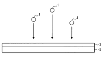
- FIG. 1 is an explanatory diagram for explaining a film forming method handled in the film forming simulation method according to the present embodiment.
- the film formation method for projecting the raw material particles 1 onto the film formation surface of the film formation target 5 to form the film 3 made of the raw material particles 1. Handle.
- the film formation simulation method according to this embodiment handles various vapor deposition methods and predicts the film quality distribution of the film to be formed.
- film forming methods that can be handled by the film forming simulation method according to the present embodiment include physical vapor deposition such as resistance heating vapor deposition, electron beam vapor deposition, molecular beam epitaxy, ion plating, and sputtering.
- Chemical vapor deposition (CVD), etc. Physical Vapor Deposition: PVD), thermal or plasma chemical vapor deposition, atomic layer deposition (ALD), metal organic chemical vapor deposition, etc. Can be illustrated.
- the raw material particles 1 are, for example, atoms, molecules, or ions obtained by ionizing these.
- the raw material particles 1 may be formed by decomposing or ionizing the raw material gas introduced into the film forming chamber using heat or plasma, or may be formed by colliding a rare gas atom or the like with a metal target. Good.
- the raw material particles 1 may be one type or two or more types. That is, the film 3 may be a film formed from a single raw material, or may be a film formed by reacting a plurality of raw materials.
- the film formation target 5 is, for example, a metal substrate, a semiconductor substrate, a glass substrate, a quartz substrate, or a resin substrate.
- the shape and material of the surface of the film formation surface of the film formation target 5 are not particularly limited. For example, a thin film may be formed on the film formation surface of the film formation target 5, or a fine structure may be formed.
- the film 3 formed on the film formation target 5 is a thin film having a thickness of about several micrometers, for example.
- the size of the region that can be handled by the film forming simulation method according to the present embodiment is, for example, a region having a side length of about several micrometers.
- the micro properties such as the density, defect density, and water permeability of the film 3 to be formed are predicted within a range of several micrometers. Is possible.
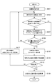
- FIG. 2 is a flowchart showing a flow of the film forming simulation method according to the present embodiment.
- initial conditions for film formation are set (S101).
- the initial conditions for film formation include information on the film formation conditions, information on the film formation surface, and the like.
- Information on the film formation conditions is, for example, information such as a film formation method, a film formation temperature, an applied power at the time of film formation, a film formation pressure, a film formation time, and a film formation speed.
- Information on the material and shape of the film formation surface is, for example, information such as a film formation method, a film formation temperature, an applied power at the time of film formation, a film formation pressure, a film formation time, and a film formation speed.
- information on the film formation conditions includes gas type, gas flux amount, film formation temperature, applied power during film formation, film formation pressure, and A film formation time or the like may be set.
- the material and shape of the film formation surface may be set as information regarding the film formation surface.
- a time step for calculating the morphology and film quality distribution of the film to be formed may be set as an initial condition.
- the raw material particles are virtually projected onto the film formation surface (S103).
- the projection direction and the projection position of the raw material particles are determined using, for example, the Monte Carlo method.
- the film-forming method is an isotropic film-forming method (for example, CVD etc.)
- the projection direction of a raw material particle is determined at random.
- the film formation method is an anisotropic film formation method (for example, PVD)
- the projection direction of the raw material particles is determined so as to have a directionality based on the film formation direction.
- the projection direction of the raw material particles may be determined so as to have a Gaussian distribution centering on the direction perpendicular to the film formation surface.
- the raw material particles projected onto the film formation surface adhere to the film formation surface (S105).
- the projected raw material particles adhere to the film formation surface with a predetermined adhesion probability (S105 / Yes).
- grains which do not adhere are reflected on the surface of a film-forming surface (S105 / No), they do not contribute to film-forming.
- the probability of adhesion of the raw material particles to the film formation surface is appropriately set based on the type and projection speed of the raw material particles and the material and reactivity of the film formation surface. You may set in the following ranges.
- the migration position of the raw material particles adhering to the film formation surface is calculated (S107).
- the raw material particles adhering to the film formation surface migrate on the surface of the film formation surface, and then form a film at the final adhesion position. In this manner, the raw material particles sequentially adhere to and accumulate on the surface of the film formation surface, whereby a film is formed on the film formation surface.
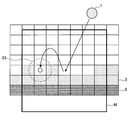
- FIG. 3 is an explanatory view showing a first calculation method of the migration position of the raw material particles.
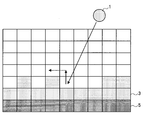
- FIG. 4 is an explanatory view showing a second calculation method of the migration position of the raw material particles.
- the state (also referred to as morphology) of a film to be formed can be modeled and expressed using cells having various shapes.
- the morphology of the film 3 on the film formation target 5 can be represented by a two-dimensional voxel model.
- the morphology of the film 3 can be modeled by a cell having another shape.
- the morphology of the film 3 may be represented by a model using polygonal or circular cells.
- the morphology of the film 3 can be represented in three dimensions, and in such a case, it may be represented by a model using a spherical or cubic cell.
- the first calculation method first, a region M in which the raw material particles 1 migrate is set, and the raw material particles 1 are finally formed on the surface of the film 3 by using the Monte Carlo method in the region M. Determine the position to adhere to.
- the region M is a region having a length L in the in-plane direction of the film formation surface with the position where the raw material particles 1 are incident as the center.
- L depends on the activation energy Ea of the film formation surface on which the raw material particles 1 are incident and the film formation temperature T, and is a value determined by, for example, Equation 1 below.
- Equation 1 D 0 is a diffusion constant, ⁇ is a diffusion time, and k B is a Boltzmann constant. Since the activation energy Ea is influenced by the surface state of the film 3 that has been formed, each time the film quality distribution of the film 3 is calculated, the film energy distribution of the film 3 is reflected again as described later. Calculated.
- the concave surface position 33 is determined whether or not the concave surface position 33 exists in the region M in which the raw material particles 1 migrate.
- the concave surface position 33 is determined as a position where the raw material particles 1 are finally attached.
- the closest concave surface position 33 from the position where the raw material particles 1 are incident is determined as the position where the raw material particles 1 are finally attached.
- the concave surface position 33 when the concave surface position 33 does not exist, it is determined that the surface position randomly selected in the region M is the position where the raw material particles 1 finally adhere.
- the surface position may be selected by weighting according to the distance from the position where the raw material particles 1 are incident.
- the raw material particles 1 are moved on the surface of the film 3 at random until the energy of the raw material particles 1 is equal to or lower than the threshold value. Determine the final attachment position above.
- the position where the energy E of the raw material particles 1 is equal to or less than the threshold is determined as the position where the raw material particles 1 are finally attached.
- Equation 2 E 0 is the initial energy that the raw material particles 1 had when they entered the film formation surface, and j is the number of times the raw material particles 1 moved on the surface of the film formation surface.
- E a is the activation energy of the film formation surface on which the raw material particles 1 are incident
- T is the film formation temperature
- k B is the Boltzmann constant. That is, the second term in Equation 2 represents the energy raw material particles 1 receives from the surrounding environment based on the deposition temperature T, the third term, the raw material particles 1 loses the activation energy E a of the deposition surface energy Represents.
- the migration position of the raw material particles can be calculated by using the first or second calculation method described above.
- the state (also referred to as morphology) of the film formed in step S111 is calculated (S111).
- the determination of whether or not a predetermined amount of raw material particles has been projected onto the film formation surface (S109) is, for example, a value obtained by multiplying the gas flux amount F 0 per unit time by a time step dt for calculating the film morphology and the like (F 0 ⁇ dt) may be determined by whether the number F t has exceeded the projected raw material particles.
- the film morphology In the calculation of the film morphology (S111), information on defects (also referred to as voids) of the film formed by the projected raw material particles is calculated. Since the raw material particles projected on the film formation surface migrate on the surface of the film formation surface, the film formed of the raw material particles grows not uniformly but unevenly. Therefore, the film formed of the raw material particles has a structure having voids. Therefore, in the calculation of the film morphology (S111), the void width of the film is calculated by calculating the structure of the film formed by the raw material particles based on the migration position on the film formation surface of the raw material particles calculated in S107. Distribution can be calculated.
- FIG. 5 is an explanatory diagram showing the morphology of the film 3 on the film formation target 5 by a two-dimensional voxel model.
- the film 3 on the film formation target 5 is unevenly grown because the raw material particles 1 projected onto the film formation surface migrate on the surface of the film formation surface.
- a void 7 is formed.
- the void width distribution representing the size and distribution of the voids 7 formed in the film 3 is calculated as the morphology of the film 3.
- the void structure of the film 3 as shown in FIG. Furthermore, by combining the void structure of the film formation surface calculated in the immediately preceding calculation step with the calculated void structure, the entire void structure of the film 3 can be calculated, and the void width distribution of the film 3 can be calculated. .
- the film quality distribution of the film formed by the raw material particles is calculated based on the film morphology (for example, void width distribution) calculated in S111 (S113).
- the film quality distribution represents at least one of a density distribution of a film formed by raw material particles and a defect density distribution.
- the density of the film or the defect density can be calculated based on the void width of the film calculated in S111, the calculation of the density of the film or the defect density for the entire film can be performed.
- a density distribution or defect density distribution can be calculated.
- the density of the film can be calculated by using the void size of the film, the composition of the raw material particles, and the film forming temperature calculated in S111.
- the defect density of the film can be calculated by using information on the film void size, raw material particle composition, film formation temperature, and film formation target (material and shape) calculated in S111.
- the film density or defect density is defined in advance by a function or database using the above-described information as a variable, and the corresponding film density or defect density can be derived by substituting the above-described information. It may be.
- a function or database for deriving the film density or defect density it is possible to reduce the amount of calculation executed by the film forming simulation method according to the present embodiment.
- the function or database for deriving the film density or defect density can be defined in advance by using, for example, approximation from actual measurement values, first-principles calculation, or MD calculation.
- the activation energy of the film surface is recalculated based on the film quality distribution of the film calculated in S113.
- the activation energy of the film surface is a parameter that changes based on the defect density distribution of the film, and the activation energy increases as the defect density of the film increases.
- the film quality distribution of the formed film is calculated, and based on the calculated film quality distribution, the value of the activation energy on the surface of the film is updated,
- the migration position of the raw material particles can be calculated by more reflecting the surface state of the film formation surface. According to this, since the calculation accuracy of the calculated migration position of the raw material particles can be improved and the void structure of the film can be calculated more accurately, the calculation accuracy of the film quality distribution of the film can be improved.
- the water permeability of the entire film formed by the raw material particles is calculated (S119).
- Moisture and the like permeate into the film by entering a minute gap existing in the formed film. Therefore, it is possible to calculate the water permeability of the film to be formed by using the void width distribution of the film to be formed.
- the water permeability of the film can be calculated by using the void width distribution of the film, the composition of the raw material particles, and the film formation temperature calculated in S113.
- the film formation simulation method can calculate the film quality distribution such as the density distribution, defect density distribution, and water permeability of the film to be formed.
- the film formation simulation method does not analyze the behavior of each atom, but uses macro parameters such as film formation conditions, it requires a huge amount of calculation and time. Without it, it is possible to predict the film quality of the film to be formed in the range of several micrometers.
- the activation energy of the film surface is recalculated at a predetermined time step, and the simulation is performed using the activation energy recalculated immediately before. According to this, since the accuracy of the activation energy of the film formation surface used for the calculation of the migration position of the raw material particles can be improved, the void structure of the film to be formed can be predicted with higher accuracy.
- the number of types of raw material particles is not particularly mentioned, but the raw material particles may be one type or two or more types.
- the raw material gas may be one kind or two or more kinds.
- the film formation method is a sputtering method, a normal sputtering method using a metal target may be used, or a reactive sputtering method using a metal target and a reactive gas may be used.
- the initial conditions for film formation further include information on the composition ratio of the raw material particles.
- the probability of adhesion between the raw material particles and the film formation surface and the activation energy are prepared for each type of raw material particle, and the migration position on the film formation surface is calculated separately for each type of raw material particle. Is done.
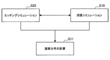
- FIG. 6 is an explanatory diagram showing an example of the linkage between the film formation simulation method according to the present embodiment and another simulation method.
- the film formation simulation method according to the present embodiment can predict the film quality distribution of a film over a plurality of manufacturing processes by being executed in conjunction with other process simulations. Specifically, the film formation simulation method according to the present embodiment can inherit information on the film model from each other with a process simulation using the same film model. According to this, since the simulation can be performed in consideration of the film quality distribution of the film on the film forming surface by taking over the information on the film model, the film quality distribution of the processed film can be predicted more accurately. it can.
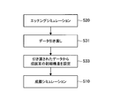
- a film formation simulation (S10) for example, during a simulation in which a film structure is modeled by a two-dimensional voxel model as shown in FIGS. 3 to 5, as shown in FIG. 6, a film formation simulation (S10) according to the present embodiment, It is possible to transfer information to and from the etching simulation (S20) and to calculate the film quality distribution (S11).
- etching simulation method that can be executed in conjunction with the film formation simulation method according to the present embodiment, for example, “Kuboi et al., Journal of Vaccum Science and Technology A 33, 061308 (2015)”.
- the disclosed plasma etching simulation method can be exemplified.
- the film formation simulation method according to the present embodiment can be executed in conjunction with, for example, another film formation simulation in addition to the etching simulation. According to this, it becomes possible to consider the film quality distribution of the film on the film formation surface in the calculation of the film quality distribution of the film to be formed.
- the first specific example is an example of predicting the film morphology and film quality distribution when a flat film made of SiN is formed using CVD.
- initial conditions were set as follows.
- a mixed gas of SiH 4 and N 2 was used as the source gas, and the gas particle flux was 10 17 particles / cm 2 ⁇ s.
- the incidence of gas particles was isotropic within a range of ⁇ 90 ° from vertically downward using a random number of [0, 1].
- the film formation temperature was 400 K
- the film formation time was 10 seconds
- the material of the film formation surface was SiO 2 .
- the film morphology was modeled by a 1 nm size two-dimensional voxel model.
- gas particles were virtually projected onto the film formation surface, and the film morphology and film quality distribution were calculated in a time step of 0.1 second. Also, based on the calculation results, the activation energy of the surface of the film formation surface was recalculated, and the recalculated activation energy value was reflected in the subsequent calculation of the gas particle migration position.
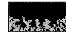
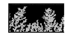
- FIG. 7A and FIG. 7B show the results of calculating the gas particle migration positions using the first calculation method described in FIG. 7A and 7B are images showing simulation results when the first calculation method described in FIG. 3 is used.
- 7A and 7B have different adhesion probabilities on the film formation surface. Specifically, FIG. 7A shows a simulation result when the adhesion probability is 0.5, and FIG. 7B shows a simulation result when the adhesion probability is 0.9.
- the morphology of the formed SiN film could be predicted by using the film formation simulation method according to this embodiment.
- 7A which has a lower adhesion probability, was found to form a morphology with a smaller void width because gas particles are more likely to diffuse to the surface of the film formation surface.
- the film density, defect density, and water permeability of the SiN film could be calculated from the morphology of the SiN film.
- FIG. 8A and 8B show the results of calculating the gas particle migration position using the second calculation method described in FIG. 8A and 8B are images showing simulation results when the second calculation method described in FIG. 4 is used. 8A and FIG. 8B have different sticking probabilities on the film formation surface. Specifically, FIG. 8A shows a simulation result when the adhesion probability is 0.5, and FIG. 8B shows a simulation result when the adhesion probability is 0.9.
- the incident gas particles migrated on the surface of the film formation surface by random numbers, and the energy in and out was calculated every time one voxel moved on the surface of the film formation surface. Threshold energy incident gas particles has finished moving, and 0.02 eV, the activation energy E a of the computation time was calculated to be approximately 2 eV.
- the morphology of the formed SiN film can be predicted as in the case of using the first calculation method. Moreover, it turned out that the morphology with smaller void width is formed in FIG. 8A having a lower adhesion probability, similar to the result calculated by the first calculation method. Further, as in the first calculation method, the film density, defect density, and water permeability of the SiN film are calculated from the morphology of the SiN film by referring to the database derived using the first principle calculation and the MD calculation. I was also able to.
- the film formation simulation method according to the present embodiment it is possible to predict the morphology and film quality of a film to be formed using information on the film formation conditions and conditions on the film formation surface.
- the film formation simulation method according to the present embodiment is not limited to the above-described SiN, and similarly for other film types such as SiO 2 and DLC (Diamond Like Carbon) films, the film morphology and film quality of the films to be formed are also the same. Can be predicted.
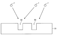
- FIG. 9 is an explanatory diagram for explaining film formation on a film formation surface on which a fine structure is formed.
- initial conditions were set as follows.
- a mixed gas of SiH 4 and N 2 or TEOS (tetraethyl orthosilicate: Si (OC 2 H 5 ) 4 ) gas was used, and the flux of gas particles was 10 17 particles / cm 2 ⁇ s.
- the incidence of gas particles was isotropic within a range of ⁇ 90 ° from vertically downward using a random number of [0, 1].
- the film formation temperature was 400 K, and the film formation time was 10 seconds.
- a trench 53 having a width of 200 nm and a depth of 500 nm is provided on the film formation surface of the film formation target 51.
- the material of the film formation target 51 was Si.
- the film morphology is modeled by a two-dimensional voxel model having a size of 1 nm, and is calculated by the same method as in the first specific example, so that the film formation target provided with the trench 53 is the same as in the first specific example. It was possible to calculate the morphology of the film formed on the film 51 and the film quality distribution.
- FIG. 10 is an explanatory diagram for explaining a film forming method having anisotropy.
- the raw material particles 1 are incident on the film forming target 5 in the incident direction having a predetermined tendency to form the film 3.
- the raw material particles 1 may be projected onto the film formation surface in the incident direction having a Gaussian distribution with the vertical direction of the film formation surface as the center.
- the anisotropy in the incident direction of the raw material particles 1 is not limited to the direction perpendicular to the film formation surface, and may be an oblique direction inclined with respect to the film formation surface.
- the distribution of the incident direction of the raw material particles 1 may be a distribution other than the Gaussian distribution.
- PVD physical vapor deposition
- the incident direction of the raw material particles 1 can be controlled by, for example, the positional relationship between the supply source of the raw material particles 1 and the film formation target 5.
- the morphology and film quality distribution of the film to be formed are calculated by using the same calculation method as in the first specific example. I was able to.
- FIGS. 11 to 12B a fourth specific example will be described with reference to FIGS. 11 to 12B.
- the fourth specific example is an example of predicting the morphology and film quality distribution of a film to be formed in consideration of damage to the film formation surface due to etching by linking the etching simulation and the film formation simulation.
- FIG. 11 is a flowchart for explaining the interlocking flow between the etching simulation and the film formation simulation.
- 12A and 12B are images showing simulation results of the etching simulation.
- the simulation result data is transferred to the film formation simulation (S31).
- the initial structure of the film-forming surface is set by extracting the morphology and film quality distribution (for example, defect density distribution, etc.) of the film-forming surface after etching from the transferred data (S33).
- the initial film formation conditions are set in addition to the set initial structure of the film formation surface, thereby calculating the film morphology and film quality distribution (S10).
- the SiN layer formed on the Si layer and the SiO 2 layer is etched,
- the SiO 2 film is formed after the sidewall processing, the morphology and film quality distribution of the formed SiO 2 can be predicted more accurately.
- the film formation surface is damaged by etching and defects are increased.
- Etching damage varies depending on the material of the film formation surface. For example, as shown in FIG. 12B, the sidewall of the slope portion formed of SiN is less damaged by etching and has a low defect density, but the upper surface and the bottom surface formed of SiO 2 are greatly damaged by etching. Defect density increases. When the defect density on the film formation surface is different, the activation energy is also different. Therefore, by receiving the defect density of the film formation surface from the etching simulation and performing the film formation simulation taking the defect density of the film formation surface into consideration, the morphology and film quality distribution of the film formed on the film formation surface can be more accurately determined. Can be calculated.
- FIG. 13 is an explanatory diagram illustrating an information processing apparatus that executes a program according to the present embodiment.
- the program according to the present embodiment is a program for executing the film forming simulation method according to the first embodiment described above.
- the program according to the present embodiment is executed by, for example, the information processing apparatus 100A illustrated in FIG. 13 or a system including the information processing apparatus 100A and the information processing server 100B.
- the program according to the present embodiment is software in which an arithmetic engine that executes calculation of the film forming simulation method according to the first embodiment is programmed.
- the program according to the present embodiment may be programmed in a programming language such as C, C ++ , Fortran, or JAVA (registered trademark).
- the present embodiment includes a storage medium that stores software (or a computer program) programmed with an arithmetic engine that executes calculation of the film forming simulation method according to the first embodiment.
- the program according to the present embodiment may be executed by the information processing apparatus 100A such as a computer, for example.
- the program according to the present embodiment may be executed by the cooperation of the information processing apparatus 100A and the information processing server 100B, for example.
- the execution speed of the film formation simulation can be improved by causing the information processing server 100B having a higher calculation capacity to execute a process with a large calculation amount in the program according to the present embodiment.
- the network 11 that connects the information processing apparatus 100A and the information processing server 100B may be a public line network such as the Internet, or a network that covers a limited narrow range such as a LAN (Local Area Network). May be.
- the network 11 may be a wired network or a wireless network as long as the information processing apparatus 100A and the information processing server 100B can be connected.
- FIG. 14 is a block diagram illustrating a functional configuration of an information processing apparatus that executes a program according to the present embodiment.
- the information processing apparatus 100 includes an input unit 101, an incident calculation unit 103, a migration calculation unit 105, a morphology calculation unit 107, a film quality calculation unit 109, an energy calculation unit 111, and a water permeability.
- a calculation unit 113 and an output unit 115 are provided.
- the execution platform of the information processing apparatus 100 that executes the program according to this embodiment is Windows (registered trademark), Linux (registered trademark), Unix (registered trademark), Mac OS (registered trademark), or OS X (registered trademark). Trademark).
- the input unit 101 receives an input of initial conditions for film formation in the film formation simulation, and transfers the input initial conditions for film formation to the incident calculation unit 103. Specifically, information such as a film forming condition, a film forming apparatus, various parameters used for calculation, structure data of a film forming surface, and a film thickness to be formed is input to the input unit 101.
- the input unit 101 may be, for example, a GUI (Graphical User Interface) displayed on a display device. Further, the configuration language of the GUI may be any of OpenGL (registered trademark), Motif, tcl / tk, and the like.
- the incident calculation unit 103 calculates the flux of the raw material particles incident on the film formation surface (that is, the number of incidents per unit time and unit area) based on the input film formation conditions. Specifically, the incident calculation unit 103 calculates the number of source particles incident on the film formation surface per unit time and unit area based on the flow rate of the incident gas, the film formation pressure, the bias voltage of the film formation surface, and the like. calculate. Further, the incident calculation unit 103 determines whether the incident direction of the raw material particles is isotropic or anisotropic, and determines the incident direction of the raw material particles.
- the migration calculation unit 105 calculates the position where the raw material particles adhering to the film formation surface finally adhere after migration. Specifically, the migration calculation unit 105 determines whether or not the raw material particles projected onto the film formation surface adhere to the film formation surface, and calculates the migration position of the raw material particles attached to the film formation surface. Since the specific calculation method executed by the migration calculation unit 105 has been described in detail in the first embodiment, the description thereof is omitted here.
- the morphology calculation unit 107 calculates the morphology of the film formed with the raw material particles projected onto the film formation surface. Specifically, when a predetermined amount of raw material particles is projected onto the film formation surface, the morphology operation unit 107 calculates the morphology of the formed film based on the migration position of the projected raw material particles. Since the specific calculation method executed by the morphology operation unit 107 has been described in detail in the first embodiment, the description thereof is omitted here.
- the film quality calculation unit 109 calculates the film quality distribution of the formed film based on the film morphology. Specifically, the film quality calculation unit 109 calculates at least one of the density distribution of the film formed by the raw material particles and the defect density distribution based on the film morphology calculated by the morphology calculation unit 107. Since the specific calculation method executed by the film quality calculation unit 109 has been described in detail in the first embodiment, description thereof is omitted here.
- the energy calculation unit 111 recalculates the activation energy of the surface of the formed film based on the film quality distribution of the formed film. Specifically, the energy calculation unit 111 uses the defect density distribution of the film calculated by the film quality calculation unit 109 to activate the surface of the film formed by a predetermined amount of raw material particles projected on the film formation surface. Calculate energy. The calculated activation energy is input to the migration calculation unit 105 and used for the subsequent calculation of the migration position of the raw material particles. Since the specific calculation method executed by the energy calculation unit 111 has been described in detail in the first embodiment, the description thereof is omitted here.
- the water permeability calculation unit 113 calculates the water permeability of the formed film based on the film quality distribution of the formed film. Specifically, the water permeability calculation unit 113 uses the film quality distribution (for example, void width distribution) of the film calculated by the film quality calculation unit 109 after the virtual film formation is completed. Calculate the water permeability. Since the specific calculation method executed by the water permeability calculation unit 113 has been described in detail in the first embodiment, the description thereof is omitted here.
- the output unit 115 outputs the calculated film morphology and film quality distribution. Specifically, the output unit 115 may output calculation results such as film morphology and film quality distribution as a data file, or may output the calculation results by visualizing the calculation results using an image such as a GUI. Any configuration language such as OpenGL, Motif, or tcl / tk can be used as the GUI configuration language. Further, the output unit 115 may output the calculated morphology and film quality distribution of the film after the calculation is completed, or may be output in real time during the calculation.
- the information processing apparatus 100 can realize the above-described functions by executing the program according to the present embodiment, and can predict the film quality distribution of a film to be formed in a range of several micrometers. It is.
- FIG. 15 is a block diagram illustrating a hardware configuration example of an information processing apparatus that executes a program according to the present embodiment.
- the information processing apparatus 100 includes a CPU (Central Processing Unit) 151, a ROM (Read Only Memory) 153, a RAM (Random Access Memory) 155, a bridge 161, internal buses 157 and 159, and the like.
- the CPU 151 functions as an arithmetic processing unit and a control unit, and controls the overall operation of the information processing apparatus 100 according to various programs (programs according to the present embodiment) stored in the ROM 153 and the like.
- the ROM 153 stores programs and calculation parameters used by the CPU 151
- the RAM 155 temporarily stores programs used in the execution of the CPU 151, parameters that change as appropriate in the execution, and the like.
- the CPU 151 may execute functions such as the incident calculation unit 103, the migration calculation unit 105, the morphology calculation unit 107, the film quality calculation unit 109, the energy calculation unit 111, and the water permeability calculation unit 113.
- the CPU 151, ROM 153, and RAM 155 are connected to each other by a bridge 161, internal buses 157 and 159, and the like.
- the CPU 151, ROM 153, and RAM 155 are also connected to an input device 165, an output device 167, a storage device 169, a drive 171, a connection port 173, and a communication device 175 via an interface 163.
- the input device 165 includes input means for inputting various information such as a touch panel, a keyboard, a mouse, a button, a microphone, a switch, and a lever.
- the input device 165 also includes an input control circuit for generating an input signal based on input or measured information and outputting it to the CPU 151.
- the input device 165 may execute the function of the input unit 101.
- the output device 167 includes, for example, a display device such as a CRT (Cathode Ray Tube) device, a liquid crystal display device and an organic electroluminescence display device, and also includes an audio output device such as a speaker and headphones.
- a display device such as a CRT (Cathode Ray Tube) device
- a liquid crystal display device such as a liquid crystal display device
- an organic electroluminescence display device such as a speaker and headphones.
- the output device 167 may execute functions such as the output unit 115.
- the storage device 169 is a data storage device configured as an example of a storage unit of the information processing device 100.
- the storage device 169 may include a storage medium, a storage device that stores data in the storage medium, a reading device that reads data from the storage medium, and a deletion device that deletes stored data.
- the drive 171 is a storage medium reader / writer, and is built in or externally attached to the information processing apparatus 100.
- the drive 171 reads information stored in a mounted removable storage medium such as a magnetic disk, an optical disk, a magneto-optical disk, or a semiconductor memory, and outputs the information to the RAM 153.
- the drive 171 can also write information on a removable storage medium.
- connection port 173 includes, for example, a connection port for connecting an external connection device such as a USB (Universal Serial Bus) port, an Ethernet (registered trademark) port, an IEEE 802.11 standard port, and an optical audio terminal. Connection interface.
- an external connection device such as a USB (Universal Serial Bus) port, an Ethernet (registered trademark) port, an IEEE 802.11 standard port, and an optical audio terminal. Connection interface.
- the communication device 175 is a communication interface configured with, for example, a communication device for connecting to the network 11. Further, the communication device 175 may be a cable communication device that performs wired cable communication, or may be a wired or wireless LAN compatible communication device.
- the film formation simulation method according to the first embodiment can be executed by the arithmetic processing device.
- FIG. 16 is an explanatory diagram for explaining the outline of the semiconductor processing system according to the present embodiment.
- the semiconductor processing system includes a semiconductor processing apparatus 300 and an information processing apparatus 200A capable of executing the film forming simulation method according to the first embodiment, or the information processing apparatus 200A and information.
- the semiconductor processing system according to this embodiment uses a film formation simulation method according to the first embodiment described above to appropriately correct a film formation condition so that a film having a desired film quality distribution can be formed. It is a processing system.
- the semiconductor processing apparatus 300 is a film forming apparatus.
- the semiconductor processing apparatus 300 may be a film forming apparatus that generates plasma by capacitively coupled plasma (CCP) or the like and forms a film on a semiconductor by CVD or PVD.
- CCP capacitively coupled plasma
- the information processing apparatus 200A is, for example, a computer or the like, and executes the film forming simulation method according to the first embodiment. Further, the information processing apparatus 200A may cause the information processing server 200B to execute a part of the calculation of the film forming simulation method according to the first embodiment. In such a case, the execution speed of the film-forming simulation can be improved by executing a process with a large calculation amount on the information processing server 200B having a higher calculation capability. Note that the network 11 that connects the information processing apparatus 200A and the information processing server 200B is the same as that described in the second embodiment, and a description thereof will be omitted.
- FIG. 17 is a block diagram showing a functional configuration of the semiconductor processing system according to the present embodiment.
- the semiconductor processing apparatus 300 includes a processing unit 301, a sensor unit 303, and a control unit 305. Further, the information processing apparatus 200 includes an incident calculation unit 203, a migration calculation unit 205, a morphology calculation unit 207, a film quality calculation unit 209, a correction determination unit 215, and a processing stop unit 217.
- the processing unit 301 is a processing chamber in which film formation is performed.
- the processing unit 301 forms a film formation target by ionizing the source gas with plasma or the like under high vacuum and projecting the ionized source gas particles onto the film formation target.
- the film forming method of the processing unit 301 is not particularly limited as long as it is a method of forming a film by projecting raw material particles as described in the first embodiment.
- the sensor unit 303 acquires information regarding the state of film formation in the processing unit 301. Specifically, the sensor unit 303 measures information about the state of the atmosphere inside the processing unit 301 and the state of the film formation target measured by the sensors included in the processing unit 301, and processes the measured information as information processing. Delivered to the device 200.
- the sensors included in the processing unit 301 include an emission analyzer (Optical Emission Spectrometry: OES), a mass spectrometer (Quadrupole SpectroMetro: QMS), an absorption spectrum analyzer (Infrared Laser Absorption Spectrum Spectral Spectral Spectral Spectral Spectral Spectral Spectroscopy) It may be an analyzer or the like.
- the sampling of the measurement result by the sensor unit 303 may be performed every 0.1 seconds, for example.
- the control unit 305 controls film forming conditions in the processing unit 301. Specifically, when the control unit 305 receives a correction condition for correcting the film formation condition from the information processing apparatus 200, the control unit 305 controls the film formation condition in the processing unit 301 based on the received correction condition. When the control unit 305 receives a processing stop instruction from the information processing apparatus 200, the control unit 305 stops the film formation in the processing unit 301. According to the control unit 305, the film formation simulation result in the information processing apparatus 200 can be reflected in the processing unit 301.
- the incident calculation unit 203 calculates the flux of the raw material particles incident on the film formation surface (that is, the number of incidents per unit time and unit area) based on the information regarding the film formation state measured by the sensor unit 303. Specifically, the incident calculation unit 203 calculates the flux of the raw material particles incident on the film formation surface based on information on the state of the atmosphere inside the processing unit 301. For example, when the film formation method is CVD, the incident calculation unit 203 calculates the flux of the raw material particles incident on the film formation surface using the gas flow rate into the chamber of the processing unit 301 and the plasma state. Also good.
- the energy calculation unit 211 calculates the activation energy of the surface of the film formation surface based on the information regarding the film formation state measured by the sensor unit 303. Specifically, the energy calculation unit 211 calculates the activation energy of the surface of the film formation surface based on information regarding the state of the film formation target. Further, when the film quality distribution of the film formed by the subsequent film quality calculation unit 209 is calculated, the energy calculation unit 211 calculates the activation energy of the surface of the film formation surface based on the calculated film quality distribution of the film. Recalculate. As a result, the information processing apparatus 200 can recalculate and update the activation energy of the surface of the film formation surface as the film formation progresses, so that the film quality distribution can be predicted more accurately.
- the migration calculation unit 205, the morphology calculation unit 207, and the film quality calculation unit 215 are substantially the same as the migration calculation unit 105, the morphology calculation unit 107, and the film quality calculation unit 115 described in the second embodiment, Individual explanation is omitted.
- the migration calculation unit 205, the morphology calculation unit 207, and the film quality calculation unit 215 calculate the film morphology and film quality distribution of the film to be formed based on the film formation state in the processing unit 301 measured by the sensor unit 303. This is different from the second embodiment.
- the correction determination unit 215 compares the film quality distribution of the film calculated by the film quality calculation unit 209 with the desired film quality distribution to determine whether the film formation condition needs to be corrected, and corrects the film formation condition. Determine the correction conditions. Specifically, when the film quality distribution of the film predicted based on the film formation state inside the processing unit 301 is different from the desired film quality distribution, the correction determination unit 215 determines the film quality distribution of the film to be formed as desired. A correction condition for approximating the film quality distribution is determined.
- the correction determination unit 215 determines the flow rate of the source gas, The film formation conditions are varied by ⁇ 50% in the order of film formation pressure, film formation temperature, film formation power, etc., and the film quality distribution is calculated again in the migration operation unit 205, the morphology operation unit 207, and the film quality operation unit 215. Let it run. Thereby, the correction determination unit 215 determines a correction condition in which the number of defects is equal to or less than a desired number of defects.
- the correction determination unit 215 can extract an appropriate condition from the database as a correction condition by searching the database.
- the correction condition determined by the correction determination unit 215 is reflected in the film formation in the processing unit 301 by being transmitted to the control unit 305 of the semiconductor processing apparatus 300.
- the process stop unit 217 stops the film formation in the semiconductor processing apparatus 300 when it is determined that a film having a desired film quality distribution cannot be formed. Specifically, when the film quality distribution of the film calculated by the film quality calculation unit 209 is greatly different from the desired film quality distribution, and the correction determination unit 215 determines that the correction condition for forming the desired film quality distribution cannot be found, The processing stop unit 217 stops film formation in the semiconductor processing apparatus 300.
- the processing stop unit 217 may be, for example, FDC / EES (Fault Detection and Classification / Equipment Engineering System). According to the processing stop unit 217, when a film having a desired film quality distribution cannot be formed, the semiconductor processing apparatus 300 is stopped at an early stage, so that an error can be dealt with early. Further, it is possible to improve the search efficiency of the film forming conditions for forming a film having a desired film quality distribution.
- the semiconductor processing system it is possible to efficiently construct processing conditions such as film formation or etching for forming a film having a desired film quality.
- the present embodiment has been described as a system including the semiconductor processing apparatus 300 and the information processing apparatus 200, but the technology according to the present disclosure is not limited to such an example.
- this embodiment may be a semiconductor processing apparatus in which the semiconductor processing apparatus 300 and the information processing apparatus 200 are integrated.
- the film thickness is reduced within a micrometer range while reflecting the film formation conditions and the film formation surface conditions. It is possible to predict film quality distribution such as density distribution, defect density distribution, and water permeability.
- the activation energy is recalculated based on the film quality distribution at each time step, and the change in the film quality distribution during the film formation is determined as the migration position of the raw material particles. It can be reflected in the calculation. Therefore, according to the film formation simulation method according to the first embodiment of the present disclosure, it is possible to improve the calculation accuracy of the morphology of the film to be formed.
- the film-forming simulation method according to the first embodiment of the present disclosure is a film quality distribution in a series of processes from film formation to etching or etching to film formation. Predictions can be made.
- the film formation simulation method according to the first embodiment of the present disclosure is processed by the information processing apparatus, thereby efficiently predicting the film quality distribution. It is possible to execute.
- the film simulation method according to (1) wherein the information related to the defect of the film includes at least information indicating a void width distribution of the film formed of the raw material particles.
- the raw material particles adhere to the film formation surface with a predetermined probability, The film formation simulation method according to (1) or (2), wherein a migration position on the film formation surface is calculated for the attached raw material particles.
- the raw material particles are two or more kinds, The film formation simulation method according to any one of (1) to (4), wherein the activation energy independent for each type of the raw material particles is used for calculating the migration position of each of the raw material particles.
- the migration position of the raw material particles is the position according to any one of (1) to (7), wherein when the raw material particles are randomly moved, the energy of the raw material particles is a threshold value or less.
- (11) The film forming simulation method according to (10), wherein the raw material particles acquire energy based on a film forming temperature for each movement and lose energy based on the activation energy at the moved position.
- a computer Based on the activation energy of the surface of the film formation surface, a computer calculates a position where each of the raw material particles incident on the film formation surface migrates on the film formation surface; Each time a migration position of a predetermined amount of the raw material particles is calculated by the migration calculation unit, a film formed of the raw material particles on the film formation surface based on the migration position of the predetermined amount of the raw material particles A morphological operation unit for calculating information on defects of Based on information on defects in the film, an energy calculation unit that calculates the activation energy of the surface of the film formed of the raw material particles, Function as The migration calculation unit uses the activation energy of the film surface calculated immediately before by the energy calculation unit.
- a migration calculation unit that calculates a position where each of the raw material particles incident on the film formation surface migrates on the film formation surface; Each time a migration position of a predetermined amount of the raw material particles is calculated, information on defects in the film formed by the raw material particles on the film formation surface is calculated based on the migration position of the predetermined amount of the raw material particles.
- a morphological operation unit to Based on information on defects in the film, an energy calculation unit that calculates the activation energy of the surface of the film formed of the raw material particles, With The migration processing unit uses the activation energy of the film surface calculated immediately before by the energy calculation unit.
- a sensor unit for measuring a film formation state A correction determination unit that determines a correction condition for correcting the film formation condition based on a difference between the film quality of the film calculated using the information measured by the sensor unit and a desired film quality; A control unit for controlling the film formation condition based on the correction condition;
- a film-forming simulation method including: (17) The film quality distribution method according to (16), wherein the film quality distribution includes at least one of a density distribution of the film and a density distribution of defects of the film. (18) The film quality distribution method according to (16) or (17), wherein the film quality distribution is calculated using a preset function or database.
- the raw material particles are two or more kinds, The film forming simulation method according to any one of (16) to (18), wherein the information on the raw material particles is a composition ratio of the raw material particles.
- (20) Calculating a position at which each of the raw material particles incident on the film-forming surface migrates on the film-forming surface based on the activation energy of the surface of the film-forming surface using an arithmetic unit; Based on the migration position of each of the raw material particles, calculating information on defects in the film formed by the raw material particles; Calculating the void width distribution of the entire film to be deposited based on information about defects in the film; Based on the void width distribution, calculating the water permeability of the entire film to be deposited;
- a film-forming simulation method including: (21) The raw material particles are two or more kinds, The film permeability simulation method according to (20), wherein the water permeability is calculated further based on a composition ratio of the raw material particles and a film formation temperature.
Landscapes
- Chemical & Material Sciences (AREA)
- Engineering & Computer Science (AREA)
- Organic Chemistry (AREA)
- Chemical Kinetics & Catalysis (AREA)
- Materials Engineering (AREA)
- Mechanical Engineering (AREA)
- Metallurgy (AREA)
- Physics & Mathematics (AREA)
- Theoretical Computer Science (AREA)
- General Chemical & Material Sciences (AREA)
- Computer Hardware Design (AREA)
- Evolutionary Computation (AREA)
- Geometry (AREA)
- General Engineering & Computer Science (AREA)
- General Physics & Mathematics (AREA)
- Chemical Vapour Deposition (AREA)
- Physical Vapour Deposition (AREA)
Priority Applications (2)
| Application Number | Priority Date | Filing Date | Title |
|---|---|---|---|
| US16/067,754 US10929579B2 (en) | 2016-01-13 | 2016-10-19 | Film formation simulation method, program, and semiconductor processing system |
| KR1020187017536A KR102671517B1 (ko) | 2016-01-13 | 2016-10-19 | 성막 시뮬레이션 방법, 프로그램 및 반도체 가공 시스템 |
Applications Claiming Priority (2)
| Application Number | Priority Date | Filing Date | Title |
|---|---|---|---|
| JP2016-004259 | 2016-01-13 | ||
| JP2016004259A JP6693133B2 (ja) | 2016-01-13 | 2016-01-13 | 成膜シミュレーション方法、プログラム、および半導体加工システム |
Publications (1)
| Publication Number | Publication Date |
|---|---|
| WO2017122404A1 true WO2017122404A1 (ja) | 2017-07-20 |
Family
ID=59311156
Family Applications (1)
| Application Number | Title | Priority Date | Filing Date |
|---|---|---|---|
| PCT/JP2016/080993 Ceased WO2017122404A1 (ja) | 2016-01-13 | 2016-10-19 | 成膜シミュレーション方法、プログラム、および半導体加工システム |
Country Status (4)
| Country | Link |
|---|---|
| US (1) | US10929579B2 (enExample) |
| JP (1) | JP6693133B2 (enExample) |
| KR (1) | KR102671517B1 (enExample) |
| WO (1) | WO2017122404A1 (enExample) |
Cited By (1)
| Publication number | Priority date | Publication date | Assignee | Title |
|---|---|---|---|---|
| WO2023238534A1 (ja) * | 2022-06-10 | 2023-12-14 | ソニーセミコンダクタソリューションズ株式会社 | 成膜シミュレーション方法、成膜シミュレーションプログラム、成膜シミュレータおよび成膜装置 |
Families Citing this family (1)
| Publication number | Priority date | Publication date | Assignee | Title |
|---|---|---|---|---|
| US12557601B2 (en) | 2019-05-07 | 2026-02-17 | Sony Semiconductor Solutions Corporation | Defect density calculation method, defect-density calculation program, defect-density calculation apparatus, heat treatment control system and machining control system |
Citations (1)
| Publication number | Priority date | Publication date | Assignee | Title |
|---|---|---|---|---|
| JP2000195766A (ja) * | 1998-12-25 | 2000-07-14 | Toshiba Corp | シミュレ―ション装置、シミュレ―ション方法、シミュレ―ションプログラムを格納した記録媒体および固体電子装置の製造方法 |
Family Cites Families (3)
| Publication number | Priority date | Publication date | Assignee | Title |
|---|---|---|---|---|
| JP2658840B2 (ja) * | 1993-12-01 | 1997-09-30 | 日本電気株式会社 | プロセスシミュレータおよびこれを用いたcvd装置およびプロセスシミュレーション方法 |
| JP4928694B2 (ja) * | 2001-09-18 | 2012-05-09 | 三菱重工業株式会社 | 薄膜多結晶の膜構造同定方法 |
| JP5428450B2 (ja) * | 2009-03-30 | 2014-02-26 | ソニー株式会社 | イオン照射ダメージの予測方法とイオン照射ダメージのシミュレータ、およびイオン照射装置とイオン照射方法 |
-
2016
- 2016-01-13 JP JP2016004259A patent/JP6693133B2/ja active Active
- 2016-10-19 KR KR1020187017536A patent/KR102671517B1/ko active Active
- 2016-10-19 US US16/067,754 patent/US10929579B2/en active Active
- 2016-10-19 WO PCT/JP2016/080993 patent/WO2017122404A1/ja not_active Ceased
Patent Citations (1)
| Publication number | Priority date | Publication date | Assignee | Title |
|---|---|---|---|---|
| JP2000195766A (ja) * | 1998-12-25 | 2000-07-14 | Toshiba Corp | シミュレ―ション装置、シミュレ―ション方法、シミュレ―ションプログラムを格納した記録媒体および固体電子装置の製造方法 |
Non-Patent Citations (2)
| Title |
|---|
| BOGICEVIC, ALEXANDER ET AL.: "Island migration caused by the motion of the atoms at the border: Size and temperature dependence of the diffusion coefficient", PHYSICAL REVIEW B, vol. 57, no. 16, 1998, pages R9459 - R9462, XP055398718 * |
| ZHU, Z. ET AL.: "Multilayer growth of BaTiO3 thin films via pulsed laser deposition: An energy-dependent kinetic Monte Carlo simulation", APPLIED SURFACE SCIENCE, vol. 256, 2010, pages 5876 - 5881, XP027076708 * |
Cited By (1)
| Publication number | Priority date | Publication date | Assignee | Title |
|---|---|---|---|---|
| WO2023238534A1 (ja) * | 2022-06-10 | 2023-12-14 | ソニーセミコンダクタソリューションズ株式会社 | 成膜シミュレーション方法、成膜シミュレーションプログラム、成膜シミュレータおよび成膜装置 |
Also Published As
| Publication number | Publication date |
|---|---|
| KR20180102551A (ko) | 2018-09-17 |
| JP6693133B2 (ja) | 2020-05-13 |
| US20190005170A1 (en) | 2019-01-03 |
| KR102671517B1 (ko) | 2024-06-04 |
| JP2017126632A (ja) | 2017-07-20 |
| US10929579B2 (en) | 2021-02-23 |
Similar Documents
| Publication | Publication Date | Title |
|---|---|---|
| JP2023511122A (ja) | 半導体製造プロセスのための性能予測子 | |
| JP2022523313A (ja) | フィーチャスケールモデリングを用いた充填プロセスの最適化 | |
| CN102201324B (zh) | 半导体制造方法与系统 | |
| WO2004032194A2 (en) | Method and system for analyzing data from a plasma process | |
| JP2010232594A (ja) | イオン照射ダメージの予測方法とイオン照射ダメージのシミュレータ、およびイオン照射装置とイオン照射方法 | |
| TW202221580A (zh) | 使用機器學習決定基板輪廓性質 | |
| TW200907731A (en) | Method and apparatus for creating a gate optimization evaluation library | |
| CN103514318A (zh) | 模拟方法、计算机可读介质、处理装置及模拟器 | |
| CN103809462A (zh) | 模拟方法及程序、模拟器、加工设备和制造半导体装置的方法 | |
| JP6693133B2 (ja) | 成膜シミュレーション方法、プログラム、および半導体加工システム | |
| JP5198519B2 (ja) | 欠陥解析方法、欠陥解析装置 | |
| Huang et al. | Intelligent manufacturing: TCAD-assisted adaptive weighting neural networks | |
| Ertl | Numerical methods for topography simulation | |
| KR100795632B1 (ko) | 시뮬레이션 장치, 시뮬레이션 프로그램을 기록한 컴퓨터판독 가능 매체, 및 시뮬레이션 방법 | |
| JP2006518925A (ja) | 半導体エッチング処理の力学的モデル化及び手法最適化のための方法およびシステム | |
| Chopra et al. | A method to accelerate creation of plasma etch recipes using physics and Bayesian statistics | |
| Liamanond et al. | Production data based optimal etch time control design for a reactive ion etching process | |
| Bobinac | Process simulation and model development in ViennaPS | |
| WO2023238534A1 (ja) | 成膜シミュレーション方法、成膜シミュレーションプログラム、成膜シミュレータおよび成膜装置 | |
| TW202328839A (zh) | 使用來自x射線能量色散光譜線掃描分析的元素圖資訊來創建處理模型 | |
| CN119585679A (zh) | 使用机器学习来决定基板轮廓性质 | |
| KR102495390B1 (ko) | 데미지 예측 방법, 프로그램, 및 반도체 가공 시스템 | |
| Liu et al. | Impact of sputtering and redeposition on the morphological profile evolution during ion-beam etching of blazed gratings | |
| TW202136943A (zh) | 半導體製造設備的控制系統及方法 | |
| Dunn et al. | Guiding gate-etch process development using 3D surface reaction modeling for 7nm and beyond |
Legal Events
| Date | Code | Title | Description |
|---|---|---|---|
| 121 | Ep: the epo has been informed by wipo that ep was designated in this application |
Ref document number: 16885007 Country of ref document: EP Kind code of ref document: A1 |
|
| ENP | Entry into the national phase |
Ref document number: 20187017536 Country of ref document: KR Kind code of ref document: A |
|
| NENP | Non-entry into the national phase |
Ref country code: DE |
|
| 122 | Ep: pct application non-entry in european phase |
Ref document number: 16885007 Country of ref document: EP Kind code of ref document: A1 |