WO2017104175A1 - 有機エレクトロルミネッセンス素子、及び、発光装置 - Google Patents
有機エレクトロルミネッセンス素子、及び、発光装置 Download PDFInfo
- Publication number
- WO2017104175A1 WO2017104175A1 PCT/JP2016/074499 JP2016074499W WO2017104175A1 WO 2017104175 A1 WO2017104175 A1 WO 2017104175A1 JP 2016074499 W JP2016074499 W JP 2016074499W WO 2017104175 A1 WO2017104175 A1 WO 2017104175A1
- Authority
- WO
- WIPO (PCT)
- Prior art keywords
- light emitting
- light
- emitting unit
- organic
- layer
- Prior art date
- Legal status (The legal status is an assumption and is not a legal conclusion. Google has not performed a legal analysis and makes no representation as to the accuracy of the status listed.)
- Ceased
Links
Images


Classifications
-
- H—ELECTRICITY
- H05—ELECTRIC TECHNIQUES NOT OTHERWISE PROVIDED FOR
- H05B—ELECTRIC HEATING; ELECTRIC LIGHT SOURCES NOT OTHERWISE PROVIDED FOR; CIRCUIT ARRANGEMENTS FOR ELECTRIC LIGHT SOURCES, IN GENERAL
- H05B33/00—Electroluminescent light sources
- H05B33/12—Light sources with substantially two-dimensional [2D] radiating surfaces
-
- H—ELECTRICITY
- H05—ELECTRIC TECHNIQUES NOT OTHERWISE PROVIDED FOR
- H05B—ELECTRIC HEATING; ELECTRIC LIGHT SOURCES NOT OTHERWISE PROVIDED FOR; CIRCUIT ARRANGEMENTS FOR ELECTRIC LIGHT SOURCES, IN GENERAL
- H05B33/00—Electroluminescent light sources
- H05B33/12—Light sources with substantially two-dimensional [2D] radiating surfaces
- H05B33/22—Light sources with substantially two-dimensional [2D] radiating surfaces characterised by the chemical or physical composition or the arrangement of auxiliary dielectric or reflective layers
- H05B33/24—Light sources with substantially two-dimensional [2D] radiating surfaces characterised by the chemical or physical composition or the arrangement of auxiliary dielectric or reflective layers of metallic reflective layers
-
- H—ELECTRICITY
- H05—ELECTRIC TECHNIQUES NOT OTHERWISE PROVIDED FOR
- H05B—ELECTRIC HEATING; ELECTRIC LIGHT SOURCES NOT OTHERWISE PROVIDED FOR; CIRCUIT ARRANGEMENTS FOR ELECTRIC LIGHT SOURCES, IN GENERAL
- H05B33/00—Electroluminescent light sources
- H05B33/12—Light sources with substantially two-dimensional [2D] radiating surfaces
- H05B33/26—Light sources with substantially two-dimensional [2D] radiating surfaces characterised by the composition or arrangement of the conductive material used as an electrode
-
- H—ELECTRICITY
- H10—SEMICONDUCTOR DEVICES; ELECTRIC SOLID-STATE DEVICES NOT OTHERWISE PROVIDED FOR
- H10K—ORGANIC ELECTRIC SOLID-STATE DEVICES
- H10K50/00—Organic light-emitting devices
- H10K50/10—OLEDs or polymer light-emitting diodes [PLED]
- H10K50/14—Carrier transporting layers
- H10K50/16—Electron transporting layers
- H10K50/166—Electron transporting layers comprising a multilayered structure
Definitions
- the present invention relates to an organic electroluminescence element and a light-emitting device provided with the organic electroluminescence element. More specifically, the present invention relates to a toned organic electroluminescence element and a light emitting device.
- Organic electroluminescence (EL) elements are self-luminous and can be reduced in thickness, power consumption is reduced, and response speed is high.
- the toning function capable of changing the emission color in the organic EL element can be an important function.
- a display device in which a toning (dimming) unit is provided in an organic EL element has been proposed (see, for example, Patent Document 1).
- the organic EL element has a problem that the longer the luminescent color, the lower the visibility and the lower the luminous efficiency. Therefore, when trying to obtain high-quality white light emission by superimposing colors, the luminance of the longest wave color (generally red) with low visibility and high power consumption is harmonized with other colors. Need to be increased. For this reason, the power consumption of an organic EL element will increase.
- the present invention provides an organic electroluminescence element and a light emitting device capable of suppressing power consumption.
- the organic EL device of the present invention is an organic electroluminescence device comprising two or more layers of light emitting units and three or more layers of electrodes sandwiching the light emitting units, the first light emitting unit and the wavelength of the first light emitting unit.
- the light-emitting device of this invention is equipped with the said organic electroluminescent element.
- an organic electroluminescence element and a light emitting device capable of suppressing power consumption.
- an organic EL element that obtains white light by providing a plurality of light emitting units and synthesizing light from each light emitting unit, the visibility of long wavelength light is lower than that of short wavelength light. For this reason, in order to obtain white light in an organic EL element, it is necessary to increase the light intensity of a light emitting unit that emits light with a long wavelength with low visibility and weaken the light intensity of other light emitting units.
- a white light emitting organic EL element the visibility of a light emitting unit that emits red light is lower than that of a light emitting unit that emits blue light, green light, and yellow light. For this reason, it is necessary to adjust the emission intensity of the red light emitting unit to be high in accordance with blue, green, and yellow light, and to adjust the emitted light to white.
- a configuration in which a microcavity (microresonator) structure is incorporated in the organic EL element can be considered.
- the microcavity structure by adjusting the thickness of the light-emitting unit, light of a specific wavelength is emphasized by resonating between the electrodes (cathode / anode), and light of other wavelengths is weakened and extracted outside.
- the spectrum can be steep and high intensity. Thereby, the brightness
- the angle dependency of the light intensity emitted from the organic EL element can be controlled.
- the light emission intensity of long-wavelength light with low visibility can be improved within a specific angle centered at 0 ° in the front direction of the organic EL element.
- the angle at which the emission intensity of short-wavelength light with high visibility is maximized can be outside (larger angle) than the angle at which the emission intensity of long-wavelength light is maximized.
- the angle (maximum intensity angle: ⁇ 1) at which the light emission intensity of the light having the longest wavelength (L1) is maximized is 0 ° in the front direction of the organic EL element. Move closer to.
- the maximum intensity angle ( ⁇ 1) of L1 is set to be equal to or smaller than the angle (maximum intensity angle: ⁇ 2) at which the emission intensity of light (L2) having the next longest wavelength after L1 is maximum.
- the angle at which the light emission intensity of L3 becomes maximum is set to be equal to or greater than the maximum intensity angle ⁇ 2.
- the maximum intensity angles ( ⁇ 1, ⁇ 2, ⁇ 3) in the light (L1, L2, L3) of each wavelength in this case are [ ⁇ 1 ⁇ ⁇ 2], [ ⁇ 1 ⁇ ⁇ 3], and [ ⁇ 2 ⁇ ⁇ 3] (that is, [ ⁇ 1 ⁇ ⁇ 2 ⁇ ⁇ 3]).
- the angle dependency of each light (L1, L2, L3) is determined.
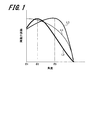
- FIG. 1 the vertical axis represents the luminance (normalized luminance) of light (L1, L2, L3) emitted from each light emitting unit, and the horizontal axis represents the luminance measurement angle in the front direction of the organic EL element.
- the angles at which the luminance is highest for the light emitted from each light emitting unit (L1, L2, L3) can be found. Further, in the graph shown in FIG. 1, the change in relative intensity of the luminance of each light according to the measurement angle can be seen.
- the light (L1) has the highest luminance at the angle ⁇ 1 because the normalized luminance at the angle ⁇ 1 is high.
- the light (L2) has the highest luminance at the angle ⁇ 2 because the normalized luminance at the angle ⁇ 2 is high
- the light (L3) has the highest normalized luminance at the angle ⁇ 3.
- the angle ⁇ 1, the angle ⁇ 2, and the angle ⁇ 3 are different values, the lights (L1, L2, and L3) have different angles having the highest luminance.
- the luminance of the light (L1) at the angle ⁇ 1 at which the luminance of the light (L1) is highest, the luminance of the light (L2) and the light (L3) does not become maximum. For this reason, at the angle ⁇ 1, the luminance of the light (L1) with low visibility becomes high, and the luminance of the light (L2) and light (L3) with high visibility becomes lower than the angles ⁇ 2 and ⁇ 3.
- the luminance of the short wavelength light (L1) with low visibility at a specific angle ⁇ 1 and reducing the light (L2) and the light (L3) in accordance with the light (L1),
- the brightness of the light (L1, L2, L3) is balanced, and high-quality white light can be obtained.
- the emission of the long wavelength light (L1) is concentrated in the front direction of the organic EL element.
- the emission of long wavelength light (L1) is concentrated in the front direction of the organic EL element, so even long wavelength light with low visibility can be observed from the center in the irradiation direction. High light intensity can be obtained within a certain angle range. For this reason, even if it is long wavelength light, high visibility can be acquired in the front direction of an organic EL element.
- the organic EL element it is preferable to provide a difference of 5 ° or more in the maximum intensity angles ⁇ 1, ⁇ 2, and ⁇ 3, and it is more preferable to provide a difference of 10 ° or more. That is, [ ⁇ 1 ⁇ 2 ⁇ 3], [ ⁇ 1 + 10 ° ⁇ ⁇ 2 + 5 ° ⁇ ⁇ 3] is more preferable, and [ ⁇ 1 + 20 ° ⁇ ⁇ 2 + 10 ° ⁇ ⁇ 3] is particularly preferable.
- the relative intensity of the long wavelength light (L1) in the front direction of the organic EL element is compared with the light (L2, L3) having a shorter wavelength than L1. It is difficult to make it large enough. For this reason, the relative intensity of the long wavelength light (L1) in the front direction of the organic EL element can be increased by increasing the difference between ⁇ 1, ⁇ 2, and ⁇ 3.
- the maximum intensity angle ( ⁇ 2, ⁇ 3) is an angle larger than the maximum intensity angle ( ⁇ 1) of the long wavelength light (L1) by utilizing the microcavity effect. [ ⁇ 1 ⁇ ⁇ 2 ⁇ ⁇ 3] is adjusted.
- the maximum intensity angle ( ⁇ 2, ⁇ 3) is adjusted to an angle [ ⁇ 1 ⁇ 2 ⁇ 3] that exceeds the maximum intensity angle ( ⁇ 1).
- the light intensity of the long wavelength light (L1) increases and the light on the short wavelength side (L2, L3) becomes relatively weak.
- the visibility of the long-wavelength light (L1) is enhanced, and the light (L1, L2, L3) is synthesized.
- white light there is no need to increase the light intensity of the long wavelength light (L1) to match the short wavelength light (L2, L3).
- visibility can be enhanced by increasing the light intensity of the long wavelength light (L1) within a certain angle in the front direction of the organic EL element due to the microcavity effect.
- white light with high light intensity and high quality can be obtained within a certain angle in the front direction of the organic EL element, so that the luminous efficiency of the organic EL element is improved and the power consumption of the organic EL element is reduced. Is possible.
- FIG. 2 shows a specific configuration of the organic EL element for explaining the design method.
- the organic EL element shown in FIG. 2 includes a transparent electrode 11, a third light emitting unit 16, a first intermediate electrode 13, a second light emitting unit 14, a second intermediate electrode 15, a first light emitting unit 12, and a reflective electrode 17. It has the structure made. That is, the organic EL element has a configuration in which three layers of light emitting units are stacked via the intermediate electrodes 13 and 15. In FIG. 2, only the configuration related to the design method of the organic EL element is shown, and the configuration of the substrate and the like is omitted.
- the first light emitting unit 12 arranged closest to the reflective electrode 17 emits light having the longest wavelength (L1). Further, the second light emitting unit 14 emits light (L2) having the next longest wavelength after L1, and the third light emitting unit 16 disposed on the side of the transparent electrode 11 emits light (L3) having the shortest wavelength. And in addition, the light emitting points in the respective light emitting units 12, 14, and 16 are h1, h2, and h3.
- a predetermined angle is obtained by the microcavity effect.
- the organic EL element is designed under the condition that the phase is strengthened in FIG. The conditions under which the phase is strengthened at this predetermined angle will be described using the configuration shown in FIGS.
- the microcavity effect depends on the wavelength ⁇ of emitted light, the refractive index n of each layer, and the optical path length.
- the wavelength ⁇ and the refractive index n of the light to be emitted are low in design freedom. Therefore, in adjusting the wavelength ⁇ and the refractive index n, the maximum intensity angles ⁇ 1, ⁇ 2, It is difficult to adjust ⁇ 3.
- the optical path length can be adjusted only by changing the thickness of the light emitting unit of the organic EL element, the degree of freedom in design is high.
- the maximum intensity angles ⁇ 1, ⁇ 2, and ⁇ 3 due to the microcavity effect are preferably adjusted by adjusting the optical path length. Therefore, in the following description, the design of an organic EL element capable of adjusting the maximum intensity angles ⁇ 1, ⁇ 2, and ⁇ 3 by adjusting the optical path length of the organic EL element will be described.
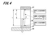
- the light from the light emitting point h has a phase change due to reflection at the reflection electrode 27, a phase change due to propagation at the light emitting unit 22, and a phase change due to reflection at the transparent electrode 21. to be influenced. Further, the phase change due to the propagation of light emitted from the light emitting point h of the light emitting unit 22 in the light emitting unit 22 is the distance d from the light emitting point h to the reflective electrode 27 and the distance from the transparent electrode 21 to the reflective electrode 27. L is affected.
- ⁇ is the wavelength in vacuum
- ⁇ EML is the angle of light inside the light emitting unit
- n EML is the refractive index of the light emitting unit
- ⁇ is the angle of light emission into the air (air angle)
- Snell's law To be related.
- the phase change ⁇ m due to reflection at the interface between the light emitting unit 22 and the reflective electrode 27 and the phase change ⁇ e due to reflection at the interface between the light emitting unit 22 and the transparent electrode 21 are functions of ⁇ EML that changes depending on the angle. It has become.
- M and l are repeating units in which the phase of light strengthens.
- the distance d at which the light of the specific wavelength ⁇ is strengthened at the specific angle ⁇ is given by the following formula (5) derived from the formula (2).
- the distance L at which the light of a specific wavelength ⁇ is strengthened at a specific angle ⁇ is given by the following formula (6) derived from the above formula (4).
- the distance d 1 from the light emitting point h1 of the first light-emitting unit 12 to the reflective electrode 17, the distance d 2 from the light emitting point h2 of the second light-emitting unit 14 to the reflective electrode 17, and, the distance d 3 to the reflecting electrode 17 from the light emitting point h3 of the third light-emitting unit 16 can be calculated by the equation (5).
- the distance d 1 from the light emitting point h1 of the first light emitting unit 12 to the reflective electrode 17 is the refractive index n1 of the first light emitting unit 12, the wavelength ⁇ 1 of the light L1 emitted from the first light emitting unit 12, And by determining the value of the maximum intensity angle ⁇ 1 of the light L1 emitted from the target first light emitting unit 12, it can be obtained from the above equation (5).
- a value for each repeating unit m corresponding to the period in which the phases strengthen is obtained from the equation (5).
- the distance d 2 from the light emitting point h2 of the second light-emitting unit 14 to the reflective electrode 17, and the distance d 3 from the light emitting point h3 to the reflective electrode 17 of the third light-emitting unit 16 also, each of the light-emitting unit 14, By determining the refractive indexes n2 and n3 of 16, the wavelengths ⁇ 2 and ⁇ 3 of the lights L2 and L3, and the maximum intensity angles ⁇ 2 and ⁇ 3 of the target lights L2 and L3, they can be obtained from the above equation (5). Also in the distances d 2 and d 3 , values are obtained from the equation (5) for each repeating unit m corresponding to the period in which the phases are strengthened.
- each light emitting unit is usually formed mainly of an organic layer material and has a refractive index of about 1.6 to 1.8, and the difference in refractive index between the light emitting units is small. For this reason, the influence on the distances d 1 , d 2 , d 3 and the distance L due to the difference in refractive index with other light emitting units is small and can be ignored. Similarly, the influence due to the difference in the refractive index of the intermediate electrode and the like can be ignored because the film thickness of the intermediate electrode is small, and the influence on the distances d 1 , d 2 , d 3 and the distance L is small.
- the distance L from the transparent electrode 11 to the reflective electrode 17 is determined by determining the respective parameters (n, ⁇ , ⁇ ) of the light L1, L2, L3. ) For each repeating unit l.
- the distance L from the transparent electrode 11 to the reflective electrode 17 is preferably matched to the light whose light intensity is to be increased most.
- the distance L from the transparent electrode 11 to the reflective electrode 17 and the distances d 1 , d 2 , d 3 from the respective light emitting points h1, h2, h3 to the reflective electrode 17 are [d 1 ⁇ d 2 ⁇ d 3
- the relationship ⁇ L] holds. Therefore, arbitrary repeating units m and l that satisfy the above relationship are selected from the distances L, d 1 , d 2 , and d 3 obtained for each repeating unit m and l, respectively. Further, the smaller distances L, d 1 , d 2 , and d 3 are advantageous in terms of productivity and cost.
- the distance L at which the light L1 having the longest wavelength is strong is preferable to select the distances d 1 , d 2 , and d 3 that satisfy the above relationship.
- the distance L, d 1, d 2, recurring units in the d 3 m, l are not each need to select the same number of cycles, the distance L, d 1, d 2, d most suitable number of cycles for each 3 Can be selected.
- the wavelength ⁇ 1 of the emitted light L1 is 620 nm, and the refractive index n1 of the first light emitting unit 12 is 1.74.
- the maximum intensity angle ⁇ 1 of the emitted light L1 and 0 ° is calculated in equation (5) and (6) air angle 0 ° at a distance phase constructive L, and d 1.
- ⁇ EML1 0 °
- ⁇ m -0.83 ⁇
- ⁇ e Equation (5) by a -0.63 ⁇
- the distance L from Equation (6) the d 1 Can be obtained as follows.
- the distances L and d 1 have a length (thickness) at which the light intensity in the 0 ° direction of the light L1 is maximized as repeating units m (m 1 , m 2 , m 3 ), l (l 1 , L 2 , l 3 ).
- the wavelength ⁇ 2 of the emitted light L2 is 530 nm
- the refractive index n2 of the second light emitting unit 14 is 1.74.
- theta EML2 10 °
- the equation (5) and (6) from the distance phase constructive L, d 2 is the following Asking.
- the wavelength ⁇ 3 of the emitted light L3 is set to 460 nm, and the refractive index n3 of the third light emitting unit 16 is set to 1.74.
- the relationship [ ⁇ 1 ( ⁇ 0 °, 620 nm light) ⁇ 2 ( ⁇ 18 °, 530 nm light) ⁇ 3 ( ⁇ 36 °, 460 nm light)) is satisfied, and [d 1 ⁇ d 2 ⁇ d 3
- An organic EL element satisfying ⁇ L> and having a small total thickness can be produced.
- the distance L was selected from the value of the light having the longest wavelength (L1) whose surface brightness is desired to be increased.
- the front luminance of long wavelength light is increased, and the power consumption of the light emitting unit is higher than the front luminance. Relatively small. Therefore, an organic EL element with low light emission efficiency and low power consumption can be realized. Further, since the front luminance of the long wavelength light is increased, the visibility of the long wavelength light is improved in the front direction of the organic EL element, and the deterioration of the panel display quality due to the color shift can be suppressed.
- the configuration of the organic EL element, the refractive index n, the emission wavelength ⁇ , and the maximum intensity angle ⁇ of each light-emitting unit are arbitrary values and can be variously changed.
- the maximum intensity angle ⁇ of each light emitting unit can be determined by examining the angle dependency of the intensity of light emitted from each light emitting unit in the formed element or panel.
- the distance d in designing the actual organic EL element is preferably within a range of ⁇ 5 nm, more preferably within a range of ⁇ 3 nm from the numerical value obtained by the above formula (5).
- the distance L in designing the actual organic EL element is obtained by the above formula (6), and is preferably within a range of ⁇ 15 nm from the selected numerical value, and is preferably within a range of ⁇ 10 nm. More preferred.
- the distance d is calculated on the assumption that the light emission position is the interface between the hole transport side and the light emitting layer.
- the distance d is about the thickness of the light emitting layer (20 This is because a difference between the calculated distance from the light emission position and the distance from the actual light emission position is assumed within a range of ( ⁇ 30 nm). In an actual organic EL element, if the numerical values of the distances d and L are formed within the above range, the effect as the above-described organic EL element can be exhibited.
- the distances d 1 , d 2 , d 3 and the distance L are preferably adjusted by the thickness of the hole transport layer or the electron transport layer of each light emitting unit. .
- the thickness is preferably adjusted with a material having high electron or hole mobility.
- the [total luminous flux / front luminance] of the first light emitting unit that emits light (L1) having the longest wavelength is set to P1. It is preferable that [P1 ⁇ P2] is satisfied, where [total luminous flux / front luminance] of the second light-emitting unit that emits light (L2) having a wavelength longer than L1 is P2.
- the organic EL element has a third light emitting unit that emits light (L3) having a shorter wavelength than the second light emitting unit, when [total luminous flux / front luminance] of the third light emitting unit is P3, It is preferable to satisfy [P1 ⁇ P2 ⁇ P3].
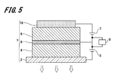
- FIG. 5 is a cross-sectional configuration diagram showing an outline of the organic EL element 1 of the embodiment.
- the organic EL element 1 shown in FIG. 5 is provided on one main surface of a transparent substrate (unknown), and in order from the transparent substrate side, the transparent electrode 2, the first light emitting unit 4, the intermediate electrode 6, and the second light emission.
- the unit 8 and the reflective electrode 10 are laminated.
- the first light-emitting unit 4 and the second light-emitting unit 8 are configured using materials having individual optical characteristics. For this reason, the first light emitting unit 4 and the second light emitting unit 8 emit light having different wavelengths.
- the organic EL element 1 takes out the first emitted light obtained in the light emitting region of the first light emitting unit 4 and the second emitted light obtained in the light emitting region of the second light emitting unit 8 from the transparent substrate side. It is configured as a bottom emission type.
- a power source 5 is connected to the transparent electrode 2 and the intermediate electrode 6 from the outside, and a power source 7 is connected to the intermediate electrode 6 and the reflective electrode 10 from the outside.
- the transparent electrode 2, the intermediate electrode 6, and the reflective electrode 10 can be independently controlled by the control unit 9 via the power supplies 5 and 7.
- the transparent substrate has optical transparency with respect to the first emitted light generated by the first light emitting unit 4 and the second emitted light generated by the second light emitting unit 8 in the visible light.
- the transparent substrate material constituting the transparent substrate include glass, quartz, and a resin substrate.
- a particularly preferable transparent substrate is a resin substrate that can give flexibility to the organic EL element 1.
- the resin substrate may be configured to have a gas barrier layer as necessary.
- a conventionally known resin material is used as the resin material constituting the resin substrate.
- acrylic resin such as acrylic acid ester, methacrylic acid ester, polymethyl methacrylate (PMMA), polyethylene terephthalate (PET), polybutylene terephthalate, polyethylene naphthalate (PEN), polycarbonate (PC), polyarylate, polyvinyl chloride ( PVC), polyethylene (PE), polypropylene (PP), polystyrene (PS), nylon (Ny), aromatic polyamide, polyether ether ketone, polysulfone, polyether sulfonate, polyimide, polyether imide, polyolefin, epoxy resin, etc.
- acrylic resin such as acrylic acid ester, methacrylic acid ester, polymethyl methacrylate (PMMA), polyethylene terephthalate (PET), polybutylene terephthalate, polyethylene naphthalate (PEN), polycarbonate (PC), polyarylate, polyvinyl chloride ( PVC), polyethylene (
- the resin film examples include cycloolefin resins and cellulose ester resins.
- a heat-resistant transparent film product name: Sila-DEC, manufactured by Chisso Corporation
- silsesquioxane having an organic-inorganic hybrid structure as a basic skeleton
- the transparent electrode 2 is in a state of being electrically connected to the intermediate electrode 6 via the power source 5.
- the transparent electrode 2 is provided as an anode or a cathode for the first light emitting unit 4.
- the transparent electrode 2 has light transmittance with respect to the first emitted light generated by the first light emitting unit 4 and the second emitted light generated by the second light emitting unit 8 in the visible light.
- the transparent electrode 2 is composed of a conductive material that is suitable as an anode or a cathode and using the above-described conductive material having excellent light transmittance.
- the conductive material suitably used for the transparent electrode 2 include transparent conductive materials such as oxide semiconductors such as ITO, ZnO, TiO 2 and SnO 2 .
- the transparent electrode 2 may be composed of a metal thin film mainly composed of metal.
- the metal thin film is a metal film having a thickness in the range of 8 to 30 nm.
- the metal contained in the metal thin film is not particularly limited as long as it is a highly conductive metal, and examples thereof include silver, copper, gold, platinum group, titanium, and chromium.
- the transparent electrode 2 may contain only one kind of these metals or two or more kinds.
- the transparent electrode 2 is preferably composed of silver as a main component and is composed of silver or an alloy containing silver as a main component.
- the alloy mainly composed of silver (Ag) constituting the transparent electrode 2 include silver magnesium (AgMg), silver copper (AgCu), silver palladium (AgPd), silver palladium copper (AgPdCu), and silver indium (AgIn). ) And the like.
- the transparent electrode 2 is composed of a metal thin film
- the transparent electrode 2 is preferably provided on the underlayer.
- the foundation layer is a layer provided on the transparent substrate side of the transparent electrode 2.
- the material constituting the underlayer is not particularly limited. For example, it preferably has an action of suppressing aggregation of silver when forming the transparent electrode 2 made of silver or an alloy containing silver as a main component. As an example, a nitrogen-containing compound or a sulfur-containing compound may be mentioned.
- the transparent electrode 2 has a sheet resistance of 30 ⁇ / sq. Or less, preferably 10 ⁇ / sq. The following is more preferable. Further, the transparent electrode 2 preferably has a light transmittance of 30% or more at a wavelength of 550 nm, more preferably 50% or more.
- the light emitting unit includes a light emitting layer configured using an organic material.
- the 1st light emission unit 4 is provided in the reflective electrode 10 side among several light emission units.
- This 1st light emission unit 4 is a laminated body containing the light emitting layer comprised at least with the organic material.
- the laminated structure of the first light emitting unit 4 is not limited, and may be any of the common laminated structures as shown in the following (i) to (vi), and further according to necessity. It may have a layer. In addition, the detail of each layer which comprises a light emission unit is mentioned later.
- the second light emitting unit 8 is disposed closer to the transparent electrode 2 than the first light emitting unit 4 among a plurality of light emitting units having a light emitting layer configured using an organic material.
- the second light emitting unit 8 is a laminate including at least a light emitting layer made of an organic material, like the first light emitting unit 4.
- the laminated structure of the second light emitting unit 8 is not limited, and may be any of the common laminated structures as shown in the examples (i) to (vi) above, and further according to necessity. It may have a layer.
- the second light emitting unit 8 may have a laminated structure different from that of the first light emitting unit 4, and the lamination order of the above (i) to (vi) may be reversed.
- the intermediate electrode 6 is provided as an anode or a cathode for the first light emitting unit 4. When the transparent electrode 2 is an anode, it is used as a cathode, and when the transparent electrode 2 is a cathode, it is used as an anode.
- the intermediate electrode 6 is also used as an anode or a cathode for the second light emitting unit 8, and is used as a cathode when the reflective electrode 10 is an anode, and is used as an anode when the reflective electrode is a cathode. Further, the intermediate electrode 6 is electrically connected to the transparent electrode 2 via the power source 5 and electrically connected to the reflective electrode 10 via the power source 7.
- the intermediate electrode 6 is composed of a material suitable for the transparent electrode 2 described above using a conductive material having excellent light transmittance.
- the intermediate electrode 6 preferably has the same sheet resistance and light transmittance as the transparent electrode 2.
- the reflective electrode 10 is provided as an anode or a cathode for the second light emitting unit 8, and is used as an anode when the intermediate electrode 6 is a cathode, and is used as a cathode when the intermediate electrode 6 is an anode.
- the reflective electrode 10 is in a state of being electrically connected to the intermediate electrode 6 via the power source 7.
- the reflective electrode 10 has good reflection characteristics with respect to the first emitted light generated by the first light emitting unit 4 and the second emitted light generated by the second light emitting unit 8 among visible light. Preferably it is.
- a reflective electrode 10 is comprised using the metal material excellent in the reflective characteristic from the electroconductive material suitable as a cathode or an anode.
- the reflective electrode 10 is made of gold, platinum, silver, copper, aluminum, or the like.
- One of the power sources 5 is connected to the transparent electrode 2 and the intermediate electrode 6.
- the power source 5 has a positive electrode connected to the anode side of the transparent electrode 2 and the intermediate electrode 6 with respect to the first light emitting unit 4 and a negative electrode connected to the cathode side.
- the other power source 7 is connected to the intermediate electrode 6 and the reflective electrode 10.
- the power source 7 has a positive electrode connected to the anode side and a negative electrode connected to the cathode side of the second light emitting unit 8 among the intermediate electrode 6 and the reflective electrode 10.
- the transparent electrode 2 is connected to the positive electrode of the power source 5 as the anode of the first light emitting unit 4, and the intermediate electrode 6 is the negative electrode of the power source 5 as the cathode of the first light emitting unit 4. It is connected to the.
- the intermediate electrode 6 is connected to the positive electrode of the power source 7 as the anode of the second light emitting unit 8
- the reflective electrode 10 is connected to the negative electrode of the power source 7 as the cathode of the second light emitting unit 8.
- the power sources 5 and 7 are configured such that the voltage and current applied to the transparent electrode 2, the intermediate electrode 6, and the reflective electrode 10 are controlled by the control unit 9.
- the control unit 9 can be configured by a computer, for example. Thereby, the light emission ratio and light emission amount of the 1st light emission unit 4 and the 2nd light emission unit 8 can be controlled, and light control property and toning property can be improved. It is also possible to control the light emission of the first light emitting unit 4 and the second light emitting unit 8 individually.
- the control unit 9 performs control to make the total of the currents supplied to the first light emitting unit 4 and the second light emitting unit 8 constant, and control to make the current of the light emitting unit with high visibility constant. By such control, it is possible to perform effective light adjustment and color adjustment of the organic EL element.
- the organic EL element 1 only needs to have at least two power supplies, but may have a larger number of power supplies. However, in order not to complicate the apparatus, it is preferable that the number of power sources is smaller than the number of electrodes.
- the organic EL element 1 preferably has a sealing material that covers from the transparent electrode 2 to the reflective electrode 10 on the transparent substrate. Furthermore, you may provide the protective member which covers this sealing material.
- the protective member is for mechanically protecting the organic EL element 1, and particularly when the sealing material is a sealing film, mechanical protection for the organic EL element 1 is not sufficient. It is preferable to provide a member.
- As the protective member a glass plate, a polymer plate, a polymer film, a metal plate, a metal film, or a polymer material film or a metal material film is applied. Among these, it is preferable to use a polymer film because it is lightweight and thin.
- the organic EL element 1 includes a light extraction layer for efficiently extracting the first emitted light and the second emitted light generated in the first light emitting unit 4 and the second light emitting unit 8 as necessary. You may have in a necessary part.
- the organic EL element 1 may have a conductive auxiliary electrode connected to the transparent electrode 2 and the intermediate electrode 6 at a position that does not overlap the light emitting region.
- the material constituting the auxiliary electrode is preferably a metal having low resistance such as gold, platinum, silver, copper, or aluminum.
- the organic EL element 1 configured as described above generates a first light emission in the light emitting region of the first light emitting unit 4 by applying a voltage in a predetermined state between the transparent electrode 2 and the intermediate electrode 6. To do. The first emitted light passes through the transparent electrode 2 and the transparent substrate, and is observed as a light emitting region on the light extraction surface side of the transparent substrate. In addition, by applying a voltage in a predetermined state between the intermediate electrode 6 and the reflective electrode 10, second emitted light is generated in the light emitting region of the second light emitting unit 8. The second emitted light passes through the transparent electrode 2 and the transparent substrate, and is observed as a light emitting region on the light extraction surface side of the transparent substrate.
- the organic EL element may be driven by applying an AC voltage, and the AC waveform to be applied may be arbitrary.
- the organic EL element described above has a configuration in which two light emitting units of the first light emitting unit 4 and the second light emitting unit 8 are stacked.
- the organic EL element 1 may have a configuration in which a plurality of light emitting units are further stacked. Even in this case, the optical characteristic relationship between the light emitting unit on the transparent electrode 2 side and the light emitting unit on the reflective electrode 10 side is the relationship between the first light emitting unit 4 and the second light emitting unit 8 described above. If it is.
- the light-emitting layer is a layer that emits light by recombination of electrons injected from the cathode side and holes injected from the anode side, and the light-emitting portion is adjacent to the light-emitting layer even in the layer of the light-emitting layer. It may be an interface with the layer to be used.
- the light emitting layer preferably contains a phosphorescent compound as a light emitting material. Note that a fluorescent material may be used as the light emitting material, or a phosphorescent compound and a fluorescent material may be used in combination.
- the light emitting layer may contain a plurality of light emitting materials.
- the light emitting layer is not particularly limited in its configuration as long as the light emitting material included satisfies the light emission requirements. Moreover, there may be a plurality of layers having the same emission spectrum and emission maximum wavelength. In this case, it is preferable to have a non-light emitting intermediate layer (not shown) between the light emitting layers.
- the total film thickness of the light emitting layer is preferably in the range of 1 to 100 nm, and more preferably in the range of 1 to 40 nm because a lower driving voltage can be obtained.
- the total film thickness of the light emitting layer includes the intermediate layer when a non-light emitting intermediate layer exists between the light emitting layers.
- the light emitting layer here is the sum of the light emitting layers in each light emitting unit not including the intermediate connector portion.
- the thickness of each light emitting layer is preferably adjusted within a range of 1 to 50 nm, and more preferably adjusted within a range of 1 to 20 nm. preferable.
- the plurality of stacked light emitting layers correspond to blue, green, and red light emitting colors, there is no particular limitation on the relationship between the film thicknesses of the blue, green, and red light emitting layers.
- the light emitting layer as described above is formed by forming a known light emitting material or host compound by a known thin film forming method such as a vacuum deposition method, a spin coating method, a casting method, an LB method, or an ink jet method. Can do.
- a known thin film forming method such as a vacuum deposition method, a spin coating method, a casting method, an LB method, or an ink jet method. Can do.
- the structure of the light-emitting layer preferably contains a host compound (also referred to as a light-emitting host) and a light-emitting material (also referred to as a light-emitting dopant), and emits light from the light-emitting material.
- Applicable light emitting dopants include, for example, International Publication No. 2005/076380, International Publication No. 2010/032663, International Publication No. 2008/140115, International Publication No. 2007/052431, International Publication No. 2011/134013, International Publication No. 2011/157339, International Publication No. 2010/086089, International Publication No. 2009/113646, International Publication No. 2012/020327, International Publication No.
- Examples of the host compound include, for example, Japanese Patent Application Laid-Open Nos. 2001-257076, 2002-308855, 2001-313179, 2002-319491, 2001-357777, JP 2002-334786, JP 2002-8860, JP 2002-334787, JP 2002-15871, 2002-334788, 2002-43056, 2002 -334789, JP 2002-75645, JP 2002-338579, JP 2002-105445, JP 2002-343568, JP 2002-141173, JP 2002-352957. No.
- the injection layer is a layer provided between the electrode and the light emitting layer in order to lower the driving voltage and improve the light emission luminance. “The organic EL element and its industrialization front line (issued by NTS, November 30, 1998) The details are described in Part 2, Chapter 2, “Electrode Materials” (pages 123 to 166) of the second edition. In the organic EL element, the injection layer includes a hole injection layer and an electron injection layer.
- the injection layer is a layer that can be provided as necessary. In the case of a hole injection layer, it is disposed between the anode and the light emitting layer or the hole transport layer, and in the case of an electron injection layer, it is disposed between the cathode and the light emitting layer or the electron transport layer.
- JP-A-9-45479 JP-A-9-260062, JP-A-8-288069 and the like.
- a phthalocyanine layer represented by copper phthalocyanine And an oxide layer typified by vanadium oxide, an amorphous carbon layer, and a polymer layer using a conductive polymer such as polyaniline (emeraldine) or polythiophene.
- the materials described in JP-T-2003-519432 can be used.
- the details of the electron injection layer are also described in JP-A-6-325871, JP-A-9-17574, JP-A-10-74586, and the like, specifically, metals represented by strontium, aluminum, and the like.
- metals represented by strontium, aluminum, and the like examples thereof include an alkali metal halide layer typified by potassium fluoride, an alkaline earth metal compound layer typified by magnesium fluoride, and an oxide layer typified by molybdenum oxide.
- the electron injection layer is preferably a very thin film, and the film thickness is preferably in the range of 1 nm to 10 ⁇ m although it depends on the material.
- the hole transport layer is made of a hole transport material having a function of transporting holes, and in a broad sense, a hole injection layer and an electron blocking layer are also included in the hole transport layer.
- the hole transport layer can be provided as a single layer or a plurality of layers.
- the hole transport material has any of the characteristics of hole injection or transport and electron barrier properties.
- the hole transport material may be either organic or inorganic.
- triazole derivatives, oxadiazole derivatives, imidazole derivatives, polyarylalkane derivatives, pyrazoline derivatives and pyrazolone derivatives, phenylenediamine derivatives, arylamine derivatives, amino-substituted chalcone derivatives, oxazole derivatives, styrylanthracene derivatives, fluorenone derivatives, hydrazone derivatives examples thereof include stilbene derivatives, silazane derivatives, aniline copolymers, conductive polymer oligomers, and thiophene oligomers.
- porphyrin compounds, aromatic tertiary amine compounds and styrylamine compounds, and aromatic tertiary amine compounds can be used.
- aromatic tertiary amine compounds and styrylamine compounds include, for example, N, N, N ′, N′-tetraphenyl-4,4′-diaminophenyl, N, N′-diphenyl-N, N '-Bis (3-methylphenyl)-[1,1'-biphenyl] -4,4'-diamine (abbreviation: TPD), 2,2-bis (4-di-p-tolylaminophenyl) propane, , 1-bis (4-di-p-tolylaminophenyl) cyclohexane, N, N, N ′, N′-tetra-p-tolyl-4,4′-diaminobiphenyl, 1,1-bis (4-di -P-tolylaminophenyl) -4-phenylcyclohexane, bis (4-dimethylamino-2-methylphenyl) phenylmethane, bis (4-di
- a polymer material in which these materials are introduced into a polymer chain or these materials are used as a polymer main chain can also be used.
- inorganic compounds such as p-type-Si and p-type-SiC can also be used as the hole injection material and the hole transport material.
- a so-called p-type hole transport material as described in 139 can also be used. These materials are preferably used because a light emitting element with higher efficiency can be obtained.
- the hole transport layer is formed by thinning the hole transport material by a known method such as a vacuum deposition method, a spin coating method, a casting method, a printing method including an ink jet method, or an LB method. Can do.
- the thickness of the hole transport layer is not particularly limited, but is usually about 5 nm to 5 ⁇ m, preferably 5 to 200 nm.
- the hole transport layer may have a single layer structure composed of one or more of the above materials.
- the hole transport layer material can be doped with impurities to increase transportability.
- impurities examples thereof include JP-A-4-297076, JP-A-2000-196140, JP-A-2001-102175, J. Pat. Appl. Phys. , 95, 5773 (2004), etc. can be applied.
- the electron transport layer is made of a material having a function of transporting electrons, and in a broad sense, an electron injection layer and a hole blocking layer (not shown) are also included in the electron transport layer.
- the electron transport layer can be provided as a single-layer structure or a multi-layer structure.
- an electron transport material constituting a layer portion adjacent to the light emitting layer emits electrons injected from the cathode. It only needs to have a function of transmitting to the layer.
- any one of conventionally known compounds can be selected and used. Examples include nitro-substituted fluorene derivatives, diphenylquinone derivatives, thiopyran dioxide derivatives, carbodiimides, fluorenylidenemethane derivatives, anthraquinodimethane, anthrone derivatives, and oxadiazole derivatives.
- a thiadiazole derivative in which the oxygen atom of the oxadiazole ring is substituted with a sulfur atom, and a quinoxaline derivative having a quinoxaline ring known as an electron-withdrawing group can also be used as a material for the electron transport layer. It can. Furthermore, a polymer material in which these materials are introduced into a polymer chain or these materials are used as a polymer main chain can also be used.
- metal complexes of 8-quinolinol derivatives such as tris (8-quinolinol) aluminum (abbreviation: Alq3), tris (5,7-dichloro-8-quinolinol) aluminum, tris (5,7-dibromo-8-quinolinol) ) Aluminum, tris (2-methyl-8-quinolinol) aluminum, tris (5-methyl-8-quinolinol) aluminum, bis (8-quinolinol) zinc (abbreviation: Znq), etc., and the central metal of these metal complexes
- a metal complex replaced with In, Mg, Cu, Ca, Sn, Ga, or Pb can also be used as a material for the electron transport layer.
- metal-free or metal phthalocyanine or those whose terminal is substituted with an alkyl group or a sulfonic acid group can be preferably used as the material for the electron transport layer.
- distyrylpyrazine derivatives exemplified as the material for the light emitting layer can also be used as the material for the electron transport layer, and n-type-Si, n-type-SiC, etc. as well as the hole injection layer and the hole transport layer.
- These inorganic semiconductors can also be used as a material for the electron transport layer.
- the electron transport layer can be formed by thinning the above material by a known method such as a vacuum deposition method, a spin coating method, a casting method, a printing method including an ink jet method, or an LB method.
- the thickness of the electron transport layer is not particularly limited, but is usually about 5 nm to 5 ⁇ m, preferably 5 to 200 nm.
- the electron transport layer may have a single layer structure composed of one or more of the above materials.
- the electron transport layer can be doped with impurities to increase transportability. Examples thereof include JP-A-4-297076, JP-A-10-270172, JP-A-2000-196140, JP-A-2001-102175, J. Pat. Appl. Phys. 95, 5773 (2004), and the like.
- the electron transport layer preferably contains potassium, a potassium compound, or the like.
- the potassium compound for example, potassium fluoride can be used.
- the same material as that for the above-described underlayer may be used. This is the same for the electron transport layer that also serves as the electron injection layer, and the same material as that for the above-described underlayer may be used.
- Electrode blocking layer / hole blocking layer examples include, for example, Japanese Patent Application Laid-Open No. 11-204258, Japanese Patent Application Laid-Open No. 11-204359, and “The Forefront of Organic EL Devices and Their Industrialization (issued by NTT Corporation on November 30, 1998). ”Page 237 and the like, there is a hole blocking (hole blocking) layer.
- the hole blocking layer has a function of an electron transport layer in a broad sense.
- the hole blocking layer is made of a hole blocking material that has a function of transporting electrons but has a very small ability to transport holes, and recombines electrons and holes by blocking holes while transporting electrons. Probability can be improved.
- the structure of an electron carrying layer can be used as a hole-blocking layer as needed.
- the hole blocking layer is preferably provided adjacent to the light emitting layer.
- the electron blocking layer has a function of a hole transport layer in a broad sense.
- the electron blocking layer is made of a material that has a function of transporting holes but has a very small ability to transport electrons, and improves the probability of recombination of electrons and holes by blocking electrons while transporting holes. be able to.
- the structure of a positive hole transport layer can be used as an electron blocking layer as needed.
- the film thickness of the hole blocking layer is preferably in the range of 3 to 100 nm, and more preferably in the range of 5 to 30 nm.
- a film formation method suitable for each member may be applied.
- film formation methods include vacuum deposition, sputtering, reactive sputtering, molecular beam epitaxy, cluster ion beam, ion plating, plasma polymerization, atmospheric pressure plasma polymerization, plasma CVD, and laser.
- film formation methods include vacuum deposition, sputtering, reactive sputtering, molecular beam epitaxy, cluster ion beam, ion plating, plasma polymerization, atmospheric pressure plasma polymerization, plasma CVD, and laser.
- CVD method a thermal CVD method, and a coating method.
- each member can be patterned into a predetermined shape by performing film formation using a mask as necessary. Each member may be patterned into a predetermined shape after each layer is formed. In addition, before and after the formation of the transparent electrode 2 and the intermediate electrode 6, an auxiliary electrode pattern may be formed as necessary.
- the laminating step is preferably performed by a procedure of forming a film from the transparent electrode 2 to the reflective electrode 10 consistently by a single evacuation.
- sealing process is performed from the reflective electrode 10 side.
- the transparent electrode 2, the intermediate electrode 6, and the terminal portion of the reflective electrode 10 are exposed, and the sealing material is covered so as to cover the laminate from the transparent electrode 2 to the reflective electrode 10 between the transparent substrate and the transparent substrate. And, if necessary, a protective member via a sealing material is bonded.
- the organic EL element 1 of the embodiment obtained as described above can be used as a planar light emitting device.
- the light emitting device can increase the area of the light emitting surface by using a plurality of organic EL elements 1.
- the light emitting surface is enlarged by arranging a plurality of organic EL elements 1 on the support substrate (that is, tiling).
- the support substrate may also serve as a sealing material, and the organic EL element 1 is sandwiched between the support electrode and the transparent substrate of the organic EL element 1 with the laminated body from the transparent electrode 2 to the reflective electrode 10 interposed therebetween. Tiling.
- An adhesive may be filled between the support substrate and the transparent substrate, thereby sealing the transparent electrode 2 to the reflective electrode 10 of the organic EL element 1. Note that the terminals of the transparent electrode 2, the intermediate electrode 6, and the reflective electrode 10 are exposed around the support substrate.
- a large-area light-emitting region obtained by connecting light-emitting regions formed in a plurality of organic EL elements can be displayed in a pattern.
- a non-light emitting region is generated at the joint of each organic EL element.
- the light extraction member a light collecting sheet or a light diffusion sheet can be used as the light extraction member.
- Organic EL elements of Samples 101 to 106 having an element area of 8 mm ⁇ 8 mm were produced by the following method.
- the organic EL element of each sample is reflected from the light emitting point of the first light emitting unit by the design method of the above embodiment so that the maximum intensity angle ( ⁇ 1, ⁇ 2, ⁇ 3) of each light emitting unit becomes a design value.
- the distance L was determined.
- the thickness of each layer of the light emitting unit of the organic EL element was adjusted so that the design values (distances) of the distances d 1 , d 2 , d 3 and the distance L were obtained.
- Table 1 below shows the maximum intensity angles ( ⁇ 1, ⁇ 2, ⁇ 3) as the design values of the organic EL elements of the samples, and the design values (distances) of the distances d 1 , d 2 , d 3 , and the distance L.
- B is a light emitting unit that emits light with a wavelength of 460 nm
- R is a light emitting unit that emits light with a wavelength of 620 nm
- G is a light emitting unit that emits light with a wavelength of 520 nm
- Y is The light emitting unit emits light having a wavelength of 580 nm.
- the second light emitting unit was formed by setting the film thickness in the same procedure using the same material as the third light emitting unit except for the light emitting layer.
- the first light emitting unit was formed by setting the film thickness in the same procedure using the same material as the third light emitting unit except for the light emitting layer.
- the laminated body from the transparent electrode to the reflective electrode is covered with a glass case from the reflective electrode side, and an epoxy-based photocurable adhesive (manufactured by Toagosei Co., Ltd.) is formed around the glass case.
- a sealing agent according to Luxtrac LC0629B was provided. The glass case and the transparent substrate were brought into close contact with each other through this sealant. Then, the laminated body from a transparent electrode to a reflective electrode was sealed by irradiating UV light from the glass case side and curing the sealing agent.
- the sealing operation with the glass case was performed in a glove box (in an atmosphere of high-purity nitrogen gas with a purity of 99.999% or more) in a nitrogen atmosphere without bringing the laminate from the transparent electrode to the reflective electrode into contact with the atmosphere. .
- the terminals of the transparent electrode, the first intermediate electrode, the second intermediate electrode, and the reflective electrode were pulled out from the glass case, and a power source was connected to these electrodes.
- an organic EL element of Sample 101 was produced.
- Organic EL elements of Samples 102 to 106 were fabricated in the same manner as Sample 101 described above except that the configuration of the light emitting unit of the organic EL element was changed as shown in Table 1. Note that the distances d 1 , d 2 , d 3 , and the distance L in the organic EL elements of the samples 102 to 106 become the thicknesses of design values by adjusting the thickness of the hole transport layer of each light emitting unit. Adjusted as follows.
- Table 1 shows the configuration of the light emitting units of the organic EL elements of samples 101 to 106 and the design value of the maximum intensity angle.
- Table 2 shows the measurement results of the organic EL elements of Samples 101 to 106.
- the measurement value similar to the design value was obtained at the maximum intensity angle of the organic EL element of each sample. Accordingly, the distance d 1 from the light emitting point of the first light emitting unit to the reflective electrode, the distance d 2 from the light emitting point of the second light emitting unit to the reflective electrode, and the third light emitting unit based on the method described in the above embodiment. Emission from each light emitting unit by adjusting the thickness of each layer of the light emitting unit of the organic EL element so that the distance d 3 from the light emitting point to the reflective electrode and the distance L from the transparent electrode to the reflective electrode The maximum intensity angle of the emitted light can be adjusted to a predetermined angle.
- Samples 101 to 104 satisfy either [ ⁇ 1 ⁇ ⁇ 2] or [ ⁇ 1 ⁇ ⁇ 3]. For this reason, the power consumption of the light emitting unit that emits the light having the longest wavelength (R or Y) can be reduced to the same level as the other colors (B, G).
- the maximum intensity angle of the third light emitting unit (G) is 0 °
- the maximum intensity angle of the second light emitting unit (R) is 20 °
- the maximum intensity angle of the first light emitting unit (B) is 0 °.
- the maximum intensity angle of the second light emitting unit (Y) is 20 °
- the maximum intensity angle of the third light emitting unit (B) is 0 °
- [ ⁇ 1 ⁇ ⁇ 2] is not satisfied. For this reason, the visibility of the long wavelength light (Y) in the front direction is lowered, and the power consumption of the second light emitting unit that emits the light (Y) is increased.
- the visibility in the front direction is improved by reducing the maximum intensity angle of the long-wavelength light
- the power consumption of the light-emitting unit that emits the long-wavelength light can be reduced. . Therefore, high efficiency and low power consumption of the organic EL element can be achieved.
Landscapes
- Electroluminescent Light Sources (AREA)
Abstract
第1発光ユニットと、第1発光ユニットよりも波長の短い光を放出する第2発光ユニットとを有し、正面方向から測定した、第1発光ユニットの発光強度が最大となる角度θ1と、第2発光ユニットの発光強度が最大となる角度θ2とが[θ1≦θ2(但し、0°≦θ1≦θ2<90°)]を満たす、消費電力の抑制が可能な有機エレクトロルミネッセンス素子を提供する。
Description
本発明は、有機エレクトロルミネッセンス素子、及び、この有機エレクトロルミネッセンス素子を備える発光装置に係わる。より詳しくは、調色可能な有機エレクトロルミネッセンス素子、及び、発光装置に係わる。
有機エレクトロルミネッセンス(electroluminescence:EL)素子は、自発光性であることから、薄型化が可能であり、消費電力が抑えられ、且つ応答速度が速いといった特徴を有している。
照明用途において、有機EL素子の発光色を変化させることができれば、色による演出を効果的に得ることができる。このため、有機EL素子において発光色を変化させることが可能な調色機能は、重要な機能となり得る。このような調色機能の一形態として、有機EL素子に調色(調光)ユニットを設けた表示装置が提案されている(例えば、特許文献1参照)。
しかしながら、有機EL素子では、長波な発光色ほど視感度が低く、発光効率が低いという課題がある。従って、色の重ね合わせにより品位の高い白色発光を得ようとすると、視感度が低く消費電力の高い最も長波な発光色(一般的には赤色系)の輝度を、他の色と調和するように高める必要がある。このため、有機EL素子の消費電力が増加してしまう。
上述した問題の解決のため、本発明においては、消費電力の抑制が可能な有機エレクトロルミネッセンス素子及び発光装置を提供するものである。
本発明の有機EL素子は、2層以上の発光ユニットと、発光ユニットを挟持する3層以上の電極とを備える有機エレクトロルミネッセンス素子であって、第1発光ユニットと、第1発光ユニットよりも波長の短い光を放出する第2発光ユニットとを有し、正面方向から測定した、第1発光ユニットの発光強度が最大となる角度θ1と、第2発光ユニットの発光強度が最大となる角度θ2とが[θ1≦θ2 (但し、0°≦θ1≦θ2<90°)]を満たす。
また、本発明の発光装置は、上記有機エレクトロルミネッセンス素子を備える。
また、本発明の発光装置は、上記有機エレクトロルミネッセンス素子を備える。
本発明によれば、消費電力の抑制が可能な有機エレクトロルミネッセンス素子及び発光装置を提供することができる。
以下、本発明を実施するための形態の例を説明するが、本発明は以下の例に限定されるものではない。
なお、説明は以下の順序で行う。
1.有機エレクトロルミネッセンス素子の概要
2.有機エレクトロルミネッセンス素子、発光装置の実施形態
なお、説明は以下の順序で行う。
1.有機エレクトロルミネッセンス素子の概要
2.有機エレクトロルミネッセンス素子、発光装置の実施形態
〈1.有機エレクトロルミネッセンス素子の概要〉
有機エレクトロルミネッセンス(EL)素子の具体的な実施形態に先立ち、本発明の有機EL素子の概要について説明する。
有機エレクトロルミネッセンス(EL)素子の具体的な実施形態に先立ち、本発明の有機EL素子の概要について説明する。
一般的に、複数の発光ユニットを設け、各発光ユニットからの光を合成することで白色光を得る有機EL素子では、長波長の光の視認性が、短波長の光よりも低い。このため、有機EL素子において白色光を得るためには、視認性の低い長波長の光を放出する発光ユニットの光強度を上げ、他の発光ユニットの光強度を弱める必要がある。
具体的には、白色発光の有機EL素子では、赤系の光を放出する発光ユニットの視認性が、青系、緑系、及び、黄系の光を放出する発光ユニットよりも低い。このため、赤系の発光ユニットの発光強度を、青系、緑系、及び、黄系の光に合わせて高く調整し、発光光を白色に調整する必要がある。
従って、一般的な上記構成の有機EL素子では、視認性の低い赤系の発光ユニットの輝度を上げるために、発光ユニットに供給する電流量を上げる必要がある。このため、有機EL素子の高効率化、低消費電力化の妨げとなる。
このような有機EL素子の課題に対して、有機EL素子にマイクロキャビティ(微小共振器)構造を取り入れる構成が考えられる。マイクロキャビティ構造では、発光ユニットの厚さを調整することにより、特定の波長の光を電極(陰極・陽極)間で共振させて強調し、それ以外の波長の光を弱め、外部に取り出される光のスペクトルを急峻かつ高強度にすることができる。これにより、有機EL素子の輝度と色純度を向上させることができる。
また、上述のマイクロキャビティ構造を利用すると、有機EL素子から放出される光強度の角度依存性の制御が可能となる。例えば、視認性の低い長波長の光の発光強度を、有機EL素子の正面方向の0°を中心とする特定角度内において向上させることができる。さらに、視認性の高い短波長の光の発光強度が最大となる角度を、長波長の光の発光強度が最大となる角度よりも外側(大きい角度)にすることができる。
従って、各発光ユニットの発光強度分布(角度依存性)において、最も波長の長い光(L1)の発光強度が最大となる角度(最大強度角度:θ1)を、有機EL素子の正面方向の0°に近づける。そして、L1の最大強度角度(θ1)を、L1の次に波長の長い光(L2)の発光強度が最大となる角度(最大強度角度:θ2)以下とする。さらに、L2よりも短波長の光(L3)を放出する発光ユニットを有する場合には、L3の発光強度が最大となる角度(最大強度角度:θ3)を、最大強度角度θ2以上とする。従って、この場合の各波長の光(L1,L2,L3)における最大強度角度(θ1,θ2,θ3)は、[θ1≦θ2]、[θ1≦θ3]、及び、[θ2≦θ3](すなわち、[θ1≦θ2≦θ3])となる。但し、[0°≦θ1≦θ2<90°]、[0°≦θ1≦θ3<90°]である。
このような、マイクロキャビティ効果によって各光(L1、L2、L3)の最大強度角度(θ1、θ2、θ3)を調整した有機EL素子において、各光(L1、L2、L3)の角度依存性の一例を図1に示す。図1は、縦軸が各発光ユニットから発光される光(L1、L2、L3)の輝度(規格化輝度)、横軸が有機EL素子の正面方向における輝度の測定角度である。図1に示すグラフでは、各発光ユニットから発光される光(L1、L2、L3)について、それぞれ輝度が最も高くなる角度がわかる。また、図1に示すグラフでは、測定角度に応じた、各光の輝度の相対的な強さの変化がわかる。
図1に示すように、光(L1)は、角度θ1での規格化輝度が高いため、角度θ1において最も高い輝度を有する。同様に、光(L2)は、角度θ2での規格化輝度が高いため、角度θ2において最も高い輝度を有し、光(L3)は、角度θ3での規格化輝度が高いため、角度θ3において最も高い輝度を有する。ここで、角度θ1、角度θ2、角度θ3はそれぞれ異なる値であるため、各光(L1、L2、L3)は、それぞれ最も高い輝度を有する角度が異なる。
すなわち、光(L1)の輝度が最も高くなる角度θ1では、光(L2)及び光(L3)の輝度は最大にならない。このため、角度θ1では、視認性の低い光(L1)の輝度が高くなり、これよりも視認性の高い光(L2)及び光(L3)の輝度が角度θ2や角度θ3よりも低くなる。このように、特定の角度θ1において、視認性の低い短波長の光(L1)の輝度を高め、この光(L1)に合わせて光(L2)及び光(L3)を低くすることにより、各光(L1、L2、L3)の輝度のバランスがとれ、品位の高い白色光を得ることができる。
ここで、長波長の光(L1)の最大強度角度(θ1)を[0°≦θ1≦5°]とすることにより、長波長の光(L1)の発光を有機EL素子の正面方向に集中させることができる。このように、マイクロキャビティ効果を利用し、長波長の光(L1)の発光を有機EL素子の正面方向に集中させることにより、視認性の低い長波長光であっても、照射方向の中心から一定の角度範囲内において高い光強度を得ることができる。このため、長波長の光であっても、有機EL素子の正面方向において、高い視認性を得ることができる。
また、有機EL素子において、最大強度角度θ1,θ2,θ3にはそれぞれ5°以上の差を設けることが好ましく、10°以上の差を設けることがより好ましい。すなわち、[θ1<θ2<θ3]であり、[θ1+10°≦θ2+5°≦θ3]がより好ましく、[θ1+20°≦θ2+10°≦θ3]が特に好ましい。
最大強度角度θ1,θ2,θ3の差が小さいと、有機EL素子の正面方向において長波長の光(L1)の相対的な強度を、L1よりも短波長の光(L2,L3)に対して十分に大きくすることが難しい。このため、θ1,θ2,θ3の差を大きくすることにより、有機EL素子の正面方向における長波長の光(L1)の相対的な強度を高めることができる。
また、短波長側の光(L2,L3)においては、マイクロキャビティ効果を利用することで、最大強度角度(θ2,θ3)を長波長の光(L1)の最大強度角度(θ1)以上の角度[θ1≦θ2≦θ3]に調整する。好ましくは、最大強度角度(θ2,θ3)が最大強度角度(θ1)を超える角度[θ1<θ2<θ3]に調整する。これにより、短波長側の光(L2,L3)は、有機EL素子の正面方向の強度が、外側の範囲の強度よりも低下する。
従って、有機EL素子の正面方向においては、長波長の光(L1)の光強度が増加し、短波長側の光(L2,L3)が相対的に弱まる。このため、長波長の光(L1)の光強度が増幅される一定の範囲(角度内)では、長波長の光(L1)の視認性が高まり、光(L1,L2,L3)の合成による白色光を得る際に、短波長の光(L2,L3)に合わせるための長波長側の光(L1)の光強度を強める必要がなくなる。
すなわち、マイクロキャビティ効果により、有機EL素子の正面方向の一定の角度内において、長波長の光(L1)の光強度を増加させることにより視認性を高めることができる。この結果、有機EL素子の正面方向の一定の角度内において、光強度が高く品位の高い白色光を得ることができるため、有機EL素子の発光効率が向上し、有機EL素子の低消費電力化が可能となる。
[設計方法]
以下、上述のマイクロキャビティ効果を利用し、[θ1≦θ2]、[θ1≦θ3]、及び、[θ2≦θ3]を実現することにより、発光効率が高く、品位の高いい白色光を得ることが可能な有機EL素子の設計方法について説明する。
以下、上述のマイクロキャビティ効果を利用し、[θ1≦θ2]、[θ1≦θ3]、及び、[θ2≦θ3]を実現することにより、発光効率が高く、品位の高いい白色光を得ることが可能な有機EL素子の設計方法について説明する。
上記設計方法を説明するための有機EL素子の具体的な構成を、図2に示す。図2に示す有機EL素子は、透明電極11、第3発光ユニット16、第1中間電極13、第2発光ユニット14、第2中間電極15、第1発光ユニット12、及び、反射電極17が積層された構成を有する。すなわち、有機EL素子は、中間電極13,15を介して3層の発光ユニットが積層された構成である。なお、図2では、有機EL素子の設計方法に係わる構成のみを記載し、基板等の構成は記載を省略している。
図2に示す有機EL素子においては、最も反射電極17側に配置された第1発光ユニット12が、最も長波長の光(L1)を放出する構成とする。また、第2発光ユニット14がL1の次に長い波長の光(L2)を放出し、最も透明電極11側に配置された第3発光ユニット16が最も短い波長の光(L3)を放出する構成とする。また、各発光ユニット12,14,16における発光点をh1、h2、h3とする。
各発光ユニット12,14,16から放出される、それぞれ波長の異なる光L1、L2、L3の最大強度角度θ1、θ2、θ3を所定の角度とするためには、マイクロキャビティ効果により、所定の角度において位相が強められる条件で有機EL素子を設計する。この所定の角度において位相が強められる条件について、図3及び図4に示す構成を用いて説明する。
図3及び図4には、透明基板20上に設けられた、透明電極21、発光ユニット22、及び、反射電極27の構成を示している。一般的にマイクロキャビティ効果は、放出される光の波長λ、各層の屈折率n、及び、光路長に依存する。なお、有機EL素子においては、発光させる光の波長λや屈折率nについては、設計の自由度が低いため、波長λや屈折率nの調整では、マイクロキャビティ効果による最大強度角度θ1、θ2、θ3の調整が難しい。一方で、光路長は、有機EL素子の発光ユニットの厚さを変えるだけで調整できるため、設計の自由度が高い。すなわち、有機EL素子において、マイクロキャビティ効果による最大強度角度θ1、θ2、θ3の調整は、光路長の調整によって行なうことが好ましい。従って、以下の説明では、有機EL素子の光路長の調整により、最大強度角度θ1、θ2、θ3を調整することが可能な有機EL素子の設計について説明する。
図3及び図4に示すように、発光点hからの光は、反射電極27での反射による位相変化、発光ユニット22での伝搬による位相変化、及び、透明電極21での反射による位相変化の影響を受ける。また、発光ユニット22の発光点hから放出される光の発光ユニット22での伝搬による位相変化は、発光点hから反射電極27までの距離d、及び、透明電極21から反射電極27までの距離Lに影響を受ける。
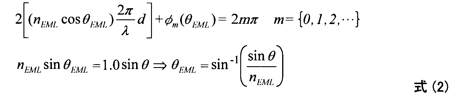
図3に示すように、反射電極27での反射による位相変化をφmとし、距離dの伝搬による位相変化を下記式(1)とすると、発光点hからの光の位相が強めあう距離dは、下記式(2)で表される。

また、図4に示すように、透明電極21での反射による位相変化を考慮し、透明電極21での反射による位相変化をφeとし、距離Lの伝搬による位相変化を下記式(3)とすると、光の位相が強めあう距離Lは、下記式(4)で表される。


なお、λは真空中の波長、θEMLは発光ユニット内部の光の角度、nEMLは発光ユニットの屈折率、θは空気中への光の出射角度(空気角度)を表し、それぞれスネルの法則に用いて関係付けられる。また、発光ユニット22と反射電極27との界面での反射による位相変化φmと、発光ユニット22と透明電極21との界面での反射による位相変化φeは角度によって変化するθEMLの関数になっている。また、m及びlは、光の位相が強めあう繰り返し単位である。
ここで、特定の波長λの光が特定の角度θにおいて強め合う距離dは、上記式(2)から導かれる下記式(5)により与えられる。

また、特定の波長λの光が特定の角度θにおいて強めあう距離Lは、上記式(4)から導かれる下記式(6)により与えられる。
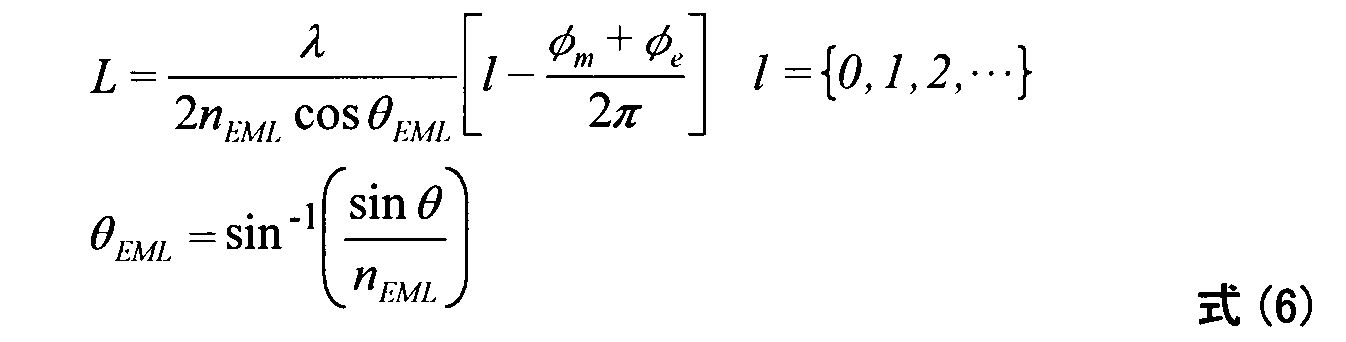
従って、発光ユニット22の屈折率n、発光波長λ、及び、要求される最大強度角度θ(θ1,θ2,θ3)の値を定めることにより、上記式(5)及び式(6)から、発光点hから反射電極27までの距離dと、透明電極21から反射電極27までの距離Lとを求めることができる。この式(5)及び式(6)は、発光ユニットが積層された構成の有機EL素子においても適用できる。
例えば、図2に示す有機EL素子においては、第1発光ユニット12の発光点h1から反射電極17までの距離d1、第2発光ユニット14の発光点h2から反射電極17までの距離d2、及び、第3発光ユニット16の発光点h3から反射電極17までの距離d3を、上記式(5)により求めることができる。
より詳細には、第1発光ユニット12の発光点h1から反射電極17までの距離d1は、第1発光ユニット12の屈折率n1、第1発光ユニット12から放出される光L1の波長λ1、及び、目的とする第1発光ユニット12から放出される光L1の最大強度角度θ1の値を定めることにより、上記式(5)から求めることができる。なお、求められる距離d1は、位相が強めあう周期に応じた、繰り返し単位m毎の値が式(5)から求められる。
同様に、第2発光ユニット14の発光点h2から反射電極17までの距離d2、及び、第3発光ユニット16の発光点h3から反射電極17までの距離d3も、それぞれの発光ユニット14,16の屈折率n2,n3、光L2,L3の波長λ2,λ3、及び、目的とする光L2,L3の最大強度角度θ2,θ3を定めることにより、上記式(5)から求めることができる。距離d2及びd3においても、位相が強めあう周期に応じた繰り返し単位m毎に、式(5)から値が求められる。
なお、各発光ユニットから放出される光は、他の発光ユニット中も通過する。このため、発光ユニット中の光の伝搬による位相変化は、光を放出した発光ユニットの屈折率だけでなく、他の発光ユニットの屈折率の影響も受ける。しかしながら、各発光ユニットは、通常、有機層系の材料を主体として形成され、屈折率が1.6~1.8程度であり、各発光ユニット同士の屈折率の差が小さい。このため、他の発光ユニットとの屈折率の差による距離d1,d2,d3、及び、距離Lへの影響は小さく、無視することができる。同様に、中間電極の屈折率の差異等による影響も、中間電極の膜厚が薄いため、距離d1,d2,d3、及び、距離Lへの影響が小さく、無視することができる。
また、図2に示す有機EL素子において、透明電極11から反射電極17までの距離Lは、光L1,L2,L3のそれぞれのパラメータ(n、λ、θ)を定めることにより、上記式(6)から繰り返し単位l毎に求められる。この場合、透明電極11から反射電極17までの距離Lは、最も光強度を高めたい光に合わせることが好ましい。ここでは、最も視認性の低い光である、最も長波長の光(L1)に合わせて透明電極11から反射電極17までの距離Lを定めることが好ましい。最も視認性の低い光の強度が高められる条件を採用することにより、有機EL素子の発光効率を向上させやすくなる。
なお、透明電極11から反射電極17までの距離Lと、各発光点h1,h2,h3から反射電極17までの距離d1,d2,d3には、[d1<d2<d3<L]の関係が成り立つ。このため、各繰り返し単位m,l毎に求められる距離L,d1,d2,d3から、上記関係が成り立つ任意の繰り返し単位m,lをそれぞれ選択する。また、距離L,d1,d2,d3は、小さい方が生産性やコスト面で有利となる。従って、最も長波長の光L1が強まる距離Lの値を選択し、且つ、上記関係が成立する距離d1,d2,d3を選択することが好ましい。なお、距離L,d1,d2,d3における繰り返し単位m,lは、それぞれ同じ周期数を選択する必要はなく、距離L,d1,d2,d3毎に最も適当な周期数を選択することができる。
[設計の具体例]
図2に示す構成の有機EL素子について、上述の式(5)及び式(6)を用いた設計方法の一例を示す。以下の説明では、[θ1≦θ2]、[θ1≦θ3]、及び、[θ2≦θ3]となるように、θ1=0°、θ2=18°、θ3=36°を設計値とする有機EL素子の設計方法について説明する。
図2に示す構成の有機EL素子について、上述の式(5)及び式(6)を用いた設計方法の一例を示す。以下の説明では、[θ1≦θ2]、[θ1≦θ3]、及び、[θ2≦θ3]となるように、θ1=0°、θ2=18°、θ3=36°を設計値とする有機EL素子の設計方法について説明する。
第1発光ユニット12において、発光光L1の波長λ1を620nm、第1発光ユニット12の屈折率n1を1.74とする。この構成において、発光光L1の最大強度角度θ1を0°とする場合には、式(5)及び式(6)から空気角度0°において位相が強めあう距離L,d1を算出する。このとき、フレネル反射率の式より、θEML1=0°、Φm=-0.83π、Φe=-0.63πとすることで式(5)及び式(6)から距離L,d1を下記のように求めることができる。下記のように、距離L,d1は、光L1の0°方向の光強度が最大となる長さ(厚さ)が繰り返し単位m(m1,m2,m3),l(l1,l2,l3)毎の値として求められる。
d1=74nm(m1=0),252nm(m1=1),430nm(m1=2),608nm(m1=3),787nm(m1=4),965nm(m1=5),1143nm(m1=6),1321nm(m1=7)……
L=130nm(l1=0),308nm(l1=1),486nm(l1=2),665nm(l1=3),843nm(l1=4),1021nm(l1=5),1199nm(l1=6),1377nm(l1=7)…
同様に、第2発光ユニット14において、発光光L2の波長λ2を530nm、第2発光ユニット14の屈折率n2を1.74とする。この構成において、発光光L2の最大強度角度θ2を18°とする場合には、θEML2=10°となり、式(5)及び式(6)から位相が強めあう距離L,d2が下記のように求められる。
d2=64nm(m2=0),217nm(m2=1),370nm(m2=2),523nm(m2=3),676nm(m2=4),829nm(m2=5),982nm(m2=6),1135nm(m2=7)…
L=112nm(l2=0),265nm(l2=1),418nm(l2=2),571nm(l2=3),724nm(l2=4),877nm(l2=5),1030nm(l2=6),1183nm(l2=7)…
さらに、第3発光ユニット16において、発光光L3の波長λ3を460nm、第3発光ユニット16の屈折率n3を1.74とする。この構成において、発光光L3の最大強度角度θ3を36°とする場合には、θEML3=20°となり、式(5)及び式(6)から位相が強めあう距離L,d3が下記のように求められる。
d3=56nm(m3=0),191nm(m3=1),326nm(m3=2),460nm(m3=3),595nm(m3=4),730nm(m3=5),865nm(m3=6),1000nm(m3=7)…
L=98nm(l3=0),233nm(l3=1),368nm(l3=2),503nm(l3=3),638nm(l3=4),772nm(l3=5),907nm(l3=6),1042nm(l3=7)…
上記のように繰り返し単位m(m1,m2,m3),l(l1,l2,l3)毎に求められた距離L,d1,d2,d3から、[d1<d2<d3<L]の関係を満たす値を選択することにより、[θ1≦θ2]、[θ1≦θ3]、及び、[θ2≦θ3]を実現することが可能な有機EL素子を設計することができる。上記の例では、L=486nm(l1=2)、d1=74nm(m1=0)、d2=217nm(m2=1)、d3=326nm(m3=2)を採用することにより、[θ1(≒0°,620nm光)<θ2(≒18°,530nm光)<θ3(≒36°,460nm光))の関係を満たし、且つ、[d1<d2<d3<L]を満たし、さらに、総厚の小さい有機EL素子を作製することができる。なお、距離Lは、表面輝度を高めたい最も長波長の光(L1)の値から選択した。
上述のように、有機EL素子の設計において上記距離L,d1,d2,d3を選択することにより、長波長の光の正面輝度が上がり、発光ユニットの消費電力が正面輝度に対して相対的に小さくなる。従って、発光効率、及び、消費電力の小さい有機EL素子を実現することができる。また、長波長の光の正面輝度が上がるため、有機EL素子の正面方向において長波長の光の視認性が向上し、色ずれによるパネル表示品位の低下を抑制することができる。
なお、有機EL素子の構成や、各発光ユニットの屈折率n、発光波長λ、最大強度角度θは、任意の値であり、種々変更可能である。一般的には、発光ユニットの数がnであり、発光の視認側から各発光ユニットを単体で発光させた場合の最大強度角度をθ1,θ2,θ3,・・・,θnとしたとき、[θ1≦θ2≦θ3≦・・・≦θn]を満たすことが好ましい。実際の有機EL素子においては、成膜した素子やパネルにおいて、発光ユニット毎に放出される光の強度の角度依存性を調べることにより、各発光ユニットの最大強度角度θを判別することができる。
また、実際の有機EL素子の設計に当たっての距離dは、上述の式(5)で求められる数値から±5nmの範囲内とすることが好ましく、±3nmの範囲内とすることがより好ましい。また、実際の有機EL素子の設計に当たっての距離Lは、上述の式(6)で求められ、選択された数値から±15nmの範囲内とすることが好ましく、±10nmの範囲内とすることがより好ましい。上述の設計例では、発光位置が正孔輸送側と発光層との界面であると想定して距離dを算出しているが、素子のキャリアバランスによっては、発光層の膜厚分程度(20~30nm)の範囲内で、計算上の発光位置からの距離と実際の発光位置からの距離との差が想定されるためである。
実際の有機EL素子において、距離d,Lの数値が上記の範囲内で形成されていれば、上述の有機EL素子としての効果を発揮することが可能である。
実際の有機EL素子において、距離d,Lの数値が上記の範囲内で形成されていれば、上述の有機EL素子としての効果を発揮することが可能である。
なお、有機EL素子の作製にあたって、距離d1,d2,d3、及び、距離Lの調整は、各発光ユニットの正孔輸送層、又は、電子輸送層の厚さで調整することが好ましい。或いは、電子又は正孔移動度の高い材料で厚さ調整することが好ましい。距離d1,d2,d3、及び、距離Lの調整に、これらの層を用いることにより、有機EL素子の電圧上昇が小さく、厚さが増加することによるデメリットを最小化できる。
また、長波長の光の正面輝度を上げ、有機EL素子の消費電力を小さくするためには、最も波長の長い光(L1)を放出する第1発光ユニットの[全光束/正面輝度 ]をP1、L1の次に長い波長の光(L2)を放出する第2発光ユニットの[全光束/正面輝度]をP2としたとき、[P1≦P2]を満たすことが好ましい。また、有機EL素子が第2発光ユニットよりも波長の短い光(L3)を放出する第3発光ユニットを有する場合には、第3発光ユニットの[全光束/正面輝度]をP3としたとき、[P1≦P2≦P3]を満たすことが好ましい。
なお、[P=全光束/正面輝度]は、光の角度依存性がランバーティアン曲線となる場合にP=3.14となる。また、正面集光タイプに近い程3.14よりも小さくなり、P=2で0°方向が長径方向の楕円となる。Pが3.14を超えると角度依存性の分布が横方向に広がり、P=4のときにいわゆるハート型形状となる。Pの大小を比較することにより、各発光ユニットにおいて正面輝度が強められているかどうかを定量的に判断することができる。
〈2.有機エレクトロルミネッセンス素子、発光装置の実施形態〉
以下、本発明の実施形態を、有機EL素子、有機EL素子の製造方法、発光装置の順に、図面に基づいて説明する。
以下、本発明の実施形態を、有機EL素子、有機EL素子の製造方法、発光装置の順に、図面に基づいて説明する。
[有機EL素子]
図5は、実施形態の有機EL素子1の概略を示す断面構成図である。
図5に示す有機EL素子1は、透明基板(不明示)の一主面上に設けられており、透明基板側から順に、透明電極2、第1発光ユニット4、中間電極6、第2発光ユニット8、及び、反射電極10が積層されている。有機EL素子1は、第1発光ユニット4と第2発光ユニット8とが、それぞれ個別の光学特性を有する材料を用いて構成されている。このため、これらの第1発光ユニット4、及び、第2発光ユニット8は、それぞれ波長の異なる光を放出する。また、有機EL素子1は、第1発光ユニット4の発光領域で得られた第1発光光と、第2発光ユニット8の発光領域で得られた第2発光光とが、透明基板側から取り出されるボトムエミッション型として構成されている。
図5は、実施形態の有機EL素子1の概略を示す断面構成図である。
図5に示す有機EL素子1は、透明基板(不明示)の一主面上に設けられており、透明基板側から順に、透明電極2、第1発光ユニット4、中間電極6、第2発光ユニット8、及び、反射電極10が積層されている。有機EL素子1は、第1発光ユニット4と第2発光ユニット8とが、それぞれ個別の光学特性を有する材料を用いて構成されている。このため、これらの第1発光ユニット4、及び、第2発光ユニット8は、それぞれ波長の異なる光を放出する。また、有機EL素子1は、第1発光ユニット4の発光領域で得られた第1発光光と、第2発光ユニット8の発光領域で得られた第2発光光とが、透明基板側から取り出されるボトムエミッション型として構成されている。
また、有機EL素子1において、透明電極2と中間電極6とには外部から電源5が接続され、中間電極6と反射電極10とには外部から電源7が接続されている。透明電極2、中間電極6、及び、反射電極10は、電源5,7を介して制御部9によってそれぞれ独立に制御可能である。
[透明基板]
透明基板は、可視光のうち特に第1発光ユニット4で発生させた第1発光光、及び、第2発光ユニット8で発生させた第2発光光に対する光透過性を有する。透明基板を構成する透明な基板材料としては、例えば、ガラス、石英、樹脂基板を挙げることができる。特に好ましい透明基板としては、有機EL素子1にフレキシブル性を与えることが可能な樹脂基板である。樹脂基板は、必要に応じてガスバリア層を有する構成であってもよい。
透明基板は、可視光のうち特に第1発光ユニット4で発生させた第1発光光、及び、第2発光ユニット8で発生させた第2発光光に対する光透過性を有する。透明基板を構成する透明な基板材料としては、例えば、ガラス、石英、樹脂基板を挙げることができる。特に好ましい透明基板としては、有機EL素子1にフレキシブル性を与えることが可能な樹脂基板である。樹脂基板は、必要に応じてガスバリア層を有する構成であってもよい。
樹脂基板を構成する樹脂材料には、従来公知の樹脂材料が用いられる。例えば、アクリル酸エステル、メタクリル酸エステル、ポリメチルメタクリレート(PMMA)等のアクリル樹脂、ポリエチレンテレフタレート(PET)、ポリブチレンテレフタレート、ポリエチレンナフタレート(PEN)、ポリカーボネート(PC)、ポリアリレート、ポリ塩化ビニル(PVC)、ポリエチレン(PE)、ポリプロピレン(PP)、ポリスチレン(PS)、ナイロン(Ny)、芳香族ポリアミド、ポリエーテルエーテルケトン、ポリスルホン、ポリエーテルスルホネート、ポリイミド、ポリエーテルイミド、ポリオレフィン、エポキシ樹脂等の各樹脂フィルムが挙げられ、さらに、シクロオレフィン系やセルロースエステル系の樹脂も用いることができる。また、有機無機ハイブリッド構造を有するシルセスキオキサンを基本骨格とした耐熱透明フィルム(製品名Sila-DEC、チッソ株式会社製)、更には樹脂材料を二層以上積層して成る樹脂フィルム等が挙げられる。
[透明電極]
透明電極2は、電源5を介して中間電極6と電気的に接続された状態となっている。透明電極2は、第1発光ユニット4に対する陽極又は陰極として設けられる。中間電極6が陰極の場合には陽極として用いられ、中間電極6が陽極の場合には陰極として用いられる。また、透明電極2は、可視光のうち、特に第1発光ユニット4で発生させた第1発光光及び、第2発光ユニット8で発生させた第2発光光に対する光透過性を有する。
透明電極2は、電源5を介して中間電極6と電気的に接続された状態となっている。透明電極2は、第1発光ユニット4に対する陽極又は陰極として設けられる。中間電極6が陰極の場合には陽極として用いられ、中間電極6が陽極の場合には陰極として用いられる。また、透明電極2は、可視光のうち、特に第1発光ユニット4で発生させた第1発光光及び、第2発光ユニット8で発生させた第2発光光に対する光透過性を有する。
透明電極2は、陽極又は陰極としてそれぞれに適切な導電性材料から、上述した光透過性に優れた導電性材料を用いて構成される。透明電極2に好適に用いられる導電性材料としては、例えばITO、ZnO、TiO2、SnO2等の酸化物半導体等の透明導電性材料が挙げられる。
また、透明電極2は、金属を主成分とした金属薄膜で構成されていてもよい。金属薄膜とは、厚さが8~30nmの範囲内の金属膜である。金属薄膜に含まれる金属は、導電性の高い金属であれば特に制限されず、例えば銀、銅、金、白金族、チタン、クロム等が例示される。透明電極2には、これらの金属が1種のみ含まれていてもよく、2種以上含まれていてもよい。
導電性の高さという観点から、透明電極2は、銀を主成分として構成され、銀又は銀を主成分とする合金で構成されていることが好ましい。透明電極2を構成する銀(Ag)を主成分とする合金としては、例えば、銀マグネシウム(AgMg)、銀銅(AgCu)、銀パラジウム(AgPd)、銀パラジウム銅(AgPdCu)、銀インジウム(AgIn)等が挙げられる。
また、透明電極2が金属薄膜から構成される場合、透明電極2が下地層上に設けられていることが好ましい。下地層は、透明電極2の透明基板側に設けられる層である。下地層を構成する材料としては、特に限定されるものではなく、例えば、銀又は銀を主成分とする合金からなる透明電極2の成膜に際し、銀の凝集を抑制する作用を有することが好ましく、一例として窒素含有化合物、又は、硫黄含有化合物等が挙げられる。
透明電極2は、シート抵抗が30Ω/sq.以下であることが好ましく、10Ω/sq.以下であることがより好ましい。また透明電極2は、波長550nmにおける光透過率が30%以上であることが好ましく、50%以上であることがより好ましい。
[発光ユニット]
発光ユニットは、有機材料を用いて構成された発光層を有する。複数の発光ユニットのうち反射電極10側に、第1発光ユニット4が設けられる。この第1発光ユニット4は、少なくとも有機材料で構成された発光層を含む積層体である。また、第1発光ユニット4の積層構造が限定されることはなく、下記(i)~(vi)に例を示すような一般的な積層構造の何れかであってよく、さらに必要に応じた層を有していてもよい。なお、発光ユニットを構成する各層の詳細は後述する。
発光ユニットは、有機材料を用いて構成された発光層を有する。複数の発光ユニットのうち反射電極10側に、第1発光ユニット4が設けられる。この第1発光ユニット4は、少なくとも有機材料で構成された発光層を含む積層体である。また、第1発光ユニット4の積層構造が限定されることはなく、下記(i)~(vi)に例を示すような一般的な積層構造の何れかであってよく、さらに必要に応じた層を有していてもよい。なお、発光ユニットを構成する各層の詳細は後述する。
(i)(陽極)/正孔注入輸送層/発光層/電子注入輸送層/(陰極)
(ii)(陽極)/正孔注入輸送層/発光層/正孔阻止層/電子注入輸送層/(陰極)
(iii)(陽極)/正孔注入輸送層/電子阻止層/発光層/正孔阻止層/電子注入輸送層/(陰極)
(iv)(陽極)/正孔注入層/正孔輸送層/発光層/電子輸送層/電子注入層/(陰極)
(v)(陽極)/正孔注入層/正孔輸送層/発光層/正孔阻止層/電子輸送層/電子注入層/(陰極)
(vi)(陽極)/正孔注入層/正孔輸送層/電子阻止層/発光層/正孔阻止層/電子輸送層/電子注入層/(陰極)
(ii)(陽極)/正孔注入輸送層/発光層/正孔阻止層/電子注入輸送層/(陰極)
(iii)(陽極)/正孔注入輸送層/電子阻止層/発光層/正孔阻止層/電子注入輸送層/(陰極)
(iv)(陽極)/正孔注入層/正孔輸送層/発光層/電子輸送層/電子注入層/(陰極)
(v)(陽極)/正孔注入層/正孔輸送層/発光層/正孔阻止層/電子輸送層/電子注入層/(陰極)
(vi)(陽極)/正孔注入層/正孔輸送層/電子阻止層/発光層/正孔阻止層/電子輸送層/電子注入層/(陰極)
第2発光ユニット8は、有機材料を用いて構成された発光層を有する複数の発光ユニットのうち第1発光ユニット4よりも透明電極2側に配置される。この第2発光ユニット8は、第1発光ユニット4と同様に少なくとも有機材料で構成された発光層を含む積層体である。また、第2発光ユニット8の積層構造が限定されることはなく、上記(i)~(vi)に例を示すような一般的な積層構造の何れかであってよく、さらに必要に応じた層を有していてもよい。また第2発光ユニット8は、第1発光ユニット4とは異なる積層構造であってもよく、上記(i)~(vi)の積層順が逆であってもよい。
[中間電極]
中間電極6は、第1発光ユニット4に対する陽極又は陰極として設けられるものであり、透明電極2が陽極の場合には陰極として用いられ、透明電極2が陰極の場合には陽極として用いられる。また中間電極6は、第2発光ユニット8に対する陽極又は陰極としても用いられるものであり、反射電極10が陽極の場合には陰極として用いられ、反射電極が陰極の場合には陽極として用いられる。また、中間電極6は、電源5を介して透明電極2と電気的に接続され、電源7を介して反射電極10と電気的に接続されている。
中間電極6は、第1発光ユニット4に対する陽極又は陰極として設けられるものであり、透明電極2が陽極の場合には陰極として用いられ、透明電極2が陰極の場合には陽極として用いられる。また中間電極6は、第2発光ユニット8に対する陽極又は陰極としても用いられるものであり、反射電極10が陽極の場合には陰極として用いられ、反射電極が陰極の場合には陽極として用いられる。また、中間電極6は、電源5を介して透明電極2と電気的に接続され、電源7を介して反射電極10と電気的に接続されている。
中間電極6は、上述の透明電極2に適する材料の中から、光透過性に優れた導電性材料を用いて構成される。中間電極6は、透明電極2と同程度のシート抵抗及び光透過率を備えていることが好ましい。
[反射電極]
反射電極10は、第2発光ユニット8に対する陽極又は陰極として設けられ、中間電極6が陰極の場合には陽極として用いられ、中間電極6が陽極の場合には陰極として用いられる。反射電極10は、電源7を介して中間電極6と電気的に接続された状態となっている。
反射電極10は、第2発光ユニット8に対する陽極又は陰極として設けられ、中間電極6が陰極の場合には陽極として用いられ、中間電極6が陽極の場合には陰極として用いられる。反射電極10は、電源7を介して中間電極6と電気的に接続された状態となっている。
反射電極10は、可視光のうち特に第1発光ユニット4で発生させた第1発光光及び、第2発光ユニット8で発生させた第2発光光に対して、良好な反射特性を有していることが好ましい。このような反射電極10は、陰極又は陽極として適切な導電性材料から、反射特性に優れた金属材料を用いて構成される。例えば反射電極10は、金、白金、銀、銅、アルミニウム等から構成される。
[電源]
電源のうち、一方の電源5は、透明電極2と中間電極6とに接続されている。この電源5は、透明電極2、及び、中間電極6のうち、第1発光ユニット4に対する陽極側にプラス極が接続され、陰極側にマイナス極を接続されている。また、他方の電源7は、中間電極6と反射電極10とに接続されている。この電源7は、中間電極6、及び、反射電極10のうち、第2発光ユニット8に対する陽極側にプラス極が接続され、陰極側にマイナス極が接続されている。
電源のうち、一方の電源5は、透明電極2と中間電極6とに接続されている。この電源5は、透明電極2、及び、中間電極6のうち、第1発光ユニット4に対する陽極側にプラス極が接続され、陰極側にマイナス極を接続されている。また、他方の電源7は、中間電極6と反射電極10とに接続されている。この電源7は、中間電極6、及び、反射電極10のうち、第2発光ユニット8に対する陽極側にプラス極が接続され、陰極側にマイナス極が接続されている。
図5に示す有機EL素子1の構成では、透明電極2が第1発光ユニット4の陽極として電源5のプラス極に接続され、中間電極6が第1発光ユニット4の陰極として電源5のマイナス極に接続されている。また、中間電極6が第2発光ユニット8の陽極として電源7のプラス極に接続され、反射電極10が第2発光ユニット8の陰極として電源7のマイナス極に接続されている。なお、第1発光ユニット4及び第2発光ユニット8の積層構造が逆の場合は、電源5,7との接続を逆にすればよい。
電源5,7は、制御部9によって透明電極2、中間電極6、及び、反射電極10に印加する電圧、及び、電流が制御される構成となっている。制御部9は、例えばコンピュータによって構成することができる。これにより、第1発光ユニット4と第2発光ユニット8の発光割合や発光量を制御することができ、調光性・調色性を高めることができる。また、第1発光ユニット4と第2発光ユニット8とを個別に発光制御することも可能である。また、制御部9は、第1発光ユニット4、及び、第2発光ユニット8への供給電流の合計を一定にする制御や、視感度の大きい発光ユニットの電流を一定にする制御を行う。このような制御によって、有機EL素子の効果的な調光・調色を行うことができる。
なお、有機EL素子1は、少なくとも2つの電源を有していればよいが、さらに多数の電源を有していてもよい。しかしながら、装置を複雑化させないため、電源は電極の数より少ないことが好ましい。
[その他の構成]
有機EL素子1には、透明基板上において、透明電極2から反射電極10までを覆う封止材を有することが好ましい。さらに、この封止材を覆う保護部材を設けてもよい。保護部材は、有機EL素子1を機械的に保護するためのものであり、特に封止材が封止膜である場合には、有機EL素子1に対する機械的な保護が十分ではないため、保護部材を設けることが好ましい。保護部材には、ガラス板、ポリマー板、ポリマーフィルム、金属板、金属フィルム、又は、ポリマー材料膜や金属材料膜が適用される。これらのうち、軽量かつ薄膜化ということからポリマーフィルムを用いることが好ましい。
有機EL素子1には、透明基板上において、透明電極2から反射電極10までを覆う封止材を有することが好ましい。さらに、この封止材を覆う保護部材を設けてもよい。保護部材は、有機EL素子1を機械的に保護するためのものであり、特に封止材が封止膜である場合には、有機EL素子1に対する機械的な保護が十分ではないため、保護部材を設けることが好ましい。保護部材には、ガラス板、ポリマー板、ポリマーフィルム、金属板、金属フィルム、又は、ポリマー材料膜や金属材料膜が適用される。これらのうち、軽量かつ薄膜化ということからポリマーフィルムを用いることが好ましい。
また、有機EL素子1は、第1発光ユニット4、及び、第2発光ユニット8において発生させた第1発光光、及び、第2発光光を効率よく取り出すための光取り出し層を、必要に応じて必要部分に有していてもよい。さらに、有機EL素子1は、発光領域と重なることのない位置において、透明電極2、及び、中間電極6に接続する導電性の良好な補助電極を有していてもよい。補助電極を構成する材料は、金、白金、銀、銅、アルミニウム等の抵抗の低い金属が好ましい。
[有機EL素子の駆動]
以上のように構成された有機EL素子1は、透明電極2と中間電極6との間に所定の状態で電圧を印加することにより、第1発光ユニット4の発光領域に第1発光光が発生する。この第1発光光は、透明電極2、及び、透明基板を透過し、透明基板の光取り出し面側で発光領域として観察される。また、中間電極6と反射電極10との間に所定の状態で電圧を印加することにより、第2発光ユニット8の発光領域に第2発光光が発生する。この第2発光光は、透明電極2、及び、透明基板を透過し、透明基板の光取り出し面側で発光領域として観察される。
以上のように構成された有機EL素子1は、透明電極2と中間電極6との間に所定の状態で電圧を印加することにより、第1発光ユニット4の発光領域に第1発光光が発生する。この第1発光光は、透明電極2、及び、透明基板を透過し、透明基板の光取り出し面側で発光領域として観察される。また、中間電極6と反射電極10との間に所定の状態で電圧を印加することにより、第2発光ユニット8の発光領域に第2発光光が発生する。この第2発光光は、透明電極2、及び、透明基板を透過し、透明基板の光取り出し面側で発光領域として観察される。
また、透明電極2、中間電極6、及び、反射電極10に所定の状態で電圧を印加した場合には、第1発光ユニット4の発光領域、及び、第2発光ユニット8の発光領域を重ね合わせた形状の発光が観察される。なお、有機EL素子の駆動は、交流電圧の印加によってもよく、印加する交流の波形は任意でよい。
[その他の変形構成]
以上説明した有機EL素子は、第1発光ユニット4、及び、第2発光ユニット8の2つの発光ユニットが積層された構成である。しかしながら、有機EL素子1は、さらに複数の発光ユニットが積層された構成であってもよい。この場合であっても、透明電極2側の発光ユニットと、それよりも反射電極10側の発光ユニットとの光学特性の関係が、上述した第1発光ユニット4と第2発光ユニット8との関係であればよい。
以上説明した有機EL素子は、第1発光ユニット4、及び、第2発光ユニット8の2つの発光ユニットが積層された構成である。しかしながら、有機EL素子1は、さらに複数の発光ユニットが積層された構成であってもよい。この場合であっても、透明電極2側の発光ユニットと、それよりも反射電極10側の発光ユニットとの光学特性の関係が、上述した第1発光ユニット4と第2発光ユニット8との関係であればよい。
[第1発光ユニット、及び、第2発光ユニットを構成する各層の材料]
第1発光ユニット4、及び、第2発光ユニット8を構成する各層の構成材料の詳細を以下に示す。第1発光ユニット4、及び、第2発光ユニット8は、以下に示す材料の中から、有機EL素子の構成に適する材料が用いられる。
第1発光ユニット4、及び、第2発光ユニット8を構成する各層の構成材料の詳細を以下に示す。第1発光ユニット4、及び、第2発光ユニット8は、以下に示す材料の中から、有機EL素子の構成に適する材料が用いられる。
[発光層]
発光層は、陰極側から注入された電子と、陽極側から注入された正孔とが再結合して発光する層であり、発光する部分は発光層の層内であっても発光層と隣接する層との界面であってもよい。発光層には発光材料としてリン光発光化合物が含有されていることが好ましい。尚、発光材料として、蛍光材料が使用されてもよいし、リン光発光化合物と蛍光材料とを併用してもよい。また、発光層は、複数の発光材料を含有してもよい。
発光層は、陰極側から注入された電子と、陽極側から注入された正孔とが再結合して発光する層であり、発光する部分は発光層の層内であっても発光層と隣接する層との界面であってもよい。発光層には発光材料としてリン光発光化合物が含有されていることが好ましい。尚、発光材料として、蛍光材料が使用されてもよいし、リン光発光化合物と蛍光材料とを併用してもよい。また、発光層は、複数の発光材料を含有してもよい。
発光層としては、含まれる発光材料が発光要件を満たしていれば、その構成には特に制限はない。また、同一の発光スペクトルや発光極大波長を有する層が複数層あってもよい。この場合、各発光層間には、非発光性の中間層(図示略)を有していることが好ましい。
発光層の膜厚の総和は1~100nmの範囲内であることが好ましく、より低い駆動電圧を得ることができることから1~40nmの範囲内であることがより好ましい。発光層の膜厚の総和とは、発光層間に非発光性の中間層が存在する場合には、中間層も含まれる。但し、中間コネクターを介して複数の発光層ユニットを積層する、いわゆるタンデム型素子の場合には、ここでいう発光層とは中間コネクター部を含まない各発光ユニット内の発光層の総和である。
複数の層を積層した構成の発光層の場合、個々の発光層の膜厚としては、1~50nmの範囲内に調整することが好ましく、更に、1~20nmの範囲内に調整することがより好ましい。積層された複数の発光層が、青、緑、赤のそれぞれの発光色に対応する場合、青、緑、赤の各発光層の膜厚の関係については、特に制限はない。
以上のような発光層は、公知の発光材料やホスト化合物を、例えば、真空蒸着法、スピンコート法、キャスト法、LB法、インクジェット法等の公知の薄膜形成方法により成膜して形成することができる。
発光層の構成としては、ホスト化合物(発光ホスト等ともいう)と、発光材料(発光ドーパントともいう)とを含有し、発光材料から発光することが好ましい。適用可能な発光ドーパントとしては、例えば、国際公開第2005/076380号、国際公開第2010/032663号、国際公開第2008/140115号、国際公開第2007/052431号、国際公開第2011/134013号、国際公開第2011/157339号、国際公開第2010/086089号、国際公開第2009/113646号、国際公開第2012/020327号、国際公開第2011/051404号、国際公開第2011/004639号、国際公開第2011/073149号、特開2012-069737号公報、特開2009-114086号公報、特開2003-81988号公報、特開2002-302671号公報、特開2002-363552号公報等に記載の化合物を挙げることができる。
また、ホスト化合物としては、例えば、特開2001-257076号公報、特開2002-308855号公報、特開2001-313179号公報、特開2002-319491号公報、特開2001-357977号公報、特開2002-334786号公報、特開2002-8860号公報、特開2002-334787号公報、特開2002-15871号公報、特開2002-334788号公報、特開2002-43056号公報、特開2002-334789号公報、特開2002-75645号公報、特開2002-338579号公報、特開2002-105445号公報、特開2002-343568号公報、特開2002-141173号公報、特開2002-352957号公報、特開2002-203683号公報、特開2002-363227号公報、特開2002-231453号公報、特開2003-3165号公報、特開2002-234888号公報、特開2003-27048号公報、特開2002-255934号公報、特開2002-260861号公報、特開2002-280183号公報、特開2002-299060号公報、特開2002-302516号公報、特開2002-305083号公報、特開2002-305084号公報、特開2002-308837号公報、米国特許公開第2003/0175553号明細書、米国特許公開第2006/0280965号明細書、米国特許公開第2005/0112407号明細書、米国特許公開第2009/0017330号明細書、米国特許公開第2009/0030202号明細書、米国特許公開第2005/238919号明細書、国際公開第2001/039234号、国際公開第2009/021126号、国際公開第2008/056746号、国際公開第2004/093207号、国際公開第2005/089025号、国際公開第2007/063796号、国際公開第2007/063754号、国際公開第2004/107822号、国際公開第2005/030900号、国際公開第2006/114966号、国際公開第2009/086028号、国際公開第2009/003898号、国際公開第2012/023947号、特開2008-074939号公報、特開2007-254297号公報、EP第2034538号明細書等に記載されている化合物を挙げることができる。
[正孔注入層/電子注入層]
注入層は、駆動電圧低下や発光輝度向上のために電極と発光層の間に設けられる層であり、「有機EL素子とその工業化最前線(1998年11月30日エヌ・ティー・エス社発行)」の第2編第2章「電極材料」(123~166頁)に、その詳細が記載されている。有機EL素子において、注入層としては正孔注入層と電子注入層とがある。
注入層は、駆動電圧低下や発光輝度向上のために電極と発光層の間に設けられる層であり、「有機EL素子とその工業化最前線(1998年11月30日エヌ・ティー・エス社発行)」の第2編第2章「電極材料」(123~166頁)に、その詳細が記載されている。有機EL素子において、注入層としては正孔注入層と電子注入層とがある。
注入層は、必要に応じて設けることができる層である。正孔注入層であれば陽極と発光層又は正孔輸送層との間、電子注入層であれば陰極と発光層又は電子輸送層との間に配置される。
正孔注入層は、特開平9-45479号公報、特開平9-260062号公報、特開平8-288069号公報等にもその詳細が記載され、具体例として、銅フタロシアニンに代表されるフタロシアニン層、酸化バナジウムに代表される酸化物層、アモルファスカーボン層、ポリアニリン(エメラルディン)やポリチオフェン等の導電性高分子を用いた高分子層等が挙げられる。また、特表2003-519432号公報に記載された材料を使用することもできる。
電子注入層は、特開平6-325871号公報、特開平9-17574号公報、特開平10-74586号公報等にもその詳細が記載され、具体的にはストロンチウムやアルミニウム等に代表される金属層、フッ化カリウムに代表されるアルカリ金属ハライド層、フッ化マグネシウムに代表されるアルカリ土類金属化合物層、酸化モリブデンに代表される酸化物層等が挙げられる。電子注入層は、ごく薄い膜であることが望ましく、素材にもよるがその膜厚は1nm~10μmの範囲が好ましい。
[正孔輸送層]
正孔輸送層は、正孔を輸送する機能を有する正孔輸送材料からなり、広い意味で正孔注入層、電子阻止層も正孔輸送層に含まれる。正孔輸送層は単層又は複数層設けることができる。正孔輸送材料としては、正孔の注入又は輸送、電子の障壁性のいずれかの特性を有する。
正孔輸送層は、正孔を輸送する機能を有する正孔輸送材料からなり、広い意味で正孔注入層、電子阻止層も正孔輸送層に含まれる。正孔輸送層は単層又は複数層設けることができる。正孔輸送材料としては、正孔の注入又は輸送、電子の障壁性のいずれかの特性を有する。
正孔輸送材料は、有機物、無機物のいずれであってもよい。例えば、トリアゾール誘導体、オキサジアゾール誘導体、イミダゾール誘導体、ポリアリールアルカン誘導体、ピラゾリン誘導体及びピラゾロン誘導体、フェニレンジアミン誘導体、アリールアミン誘導体、アミノ置換カルコン誘導体、オキサゾール誘導体、スチリルアントラセン誘導体、フルオレノン誘導体、ヒドラゾン誘導体、スチルベン誘導体、シラザン誘導体、アニリン系共重合体、導電性高分子オリゴマー、チオフェンオリゴマー等が挙げられる。更に、ポルフィリン化合物、芳香族第3級アミン化合物及びスチリルアミン化合物、芳香族第3級アミン化合物を用いることができる。
芳香族第3級アミン化合物及びスチリルアミン化合物の代表例としては、例えば、N,N,N′,N′-テトラフェニル-4,4′-ジアミノフェニル、N,N′-ジフェニル-N,N′-ビス(3-メチルフェニル)-〔1,1′-ビフェニル〕-4,4′-ジアミン(略称:TPD)、2,2-ビス(4-ジ-p-トリルアミノフェニル)プロパン、1,1-ビス(4-ジ-p-トリルアミノフェニル)シクロヘキサン、N,N,N′,N′-テトラ-p-トリル-4,4′-ジアミノビフェニル、1,1-ビス(4-ジ-p-トリルアミノフェニル)-4-フェニルシクロヘキサン、ビス(4-ジメチルアミノ-2-メチルフェニル)フェニルメタン、ビス(4-ジ-p-トリルアミノフェニル)フェニルメタン、N,N′-ジフェニル-N,N′-ジ(4-メトキシフェニル)-4,4′-ジアミノビフェニル、N,N,N′,N′-テトラフェニル-4,4′-ジアミノジフェニルエーテル、4,4′-ビス(ジフェニルアミノ)クオードリフェニル、N,N,N-トリ(p-トリル)アミン、4-(ジ-p-トリルアミノ)-4′-〔4-(ジ-p-トリルアミノ)スチリル〕スチルベン、4-N,N-ジフェニルアミノ-(2-ジフェニルビニル)ベンゼン、3-メトキシ-4′-N,N-ジフェニルアミノスチルベンゼン、N-フェニルカルバゾール、さらには米国特許第5061569号明細書に記載されている2個の縮合芳香族環を分子内に有する、例えば、4,4′-ビス〔N-(1-ナフチル)-N-フェニルアミノ〕ビフェニル(略称:NPD)、特開平4-308688号公報に記載されているトリフェニルアミンユニットが3つスターバースト型に連結された4,4′,4″-トリス〔N-(3-メチルフェニル)-N-フェニルアミノ〕トリフェニルアミン(略称:MTDATA)等が挙げられる。
さらに、これらの材料を高分子鎖に導入した、又は、これらの材料を高分子の主鎖とした高分子材料を用いることもできる。また、p型-Si、p型-SiC等の無機化合物も正孔注入材料、正孔輸送材料として使用することができる。また、特開平11-251067号公報、J.Huang et.al.,Applied Physics Letters,80(2002),p.139に記載されているような、いわゆるp型正孔輸送材料を用いることもできる。より高効率の発光素子が得られることから、これらの材料を用いることが好ましい。
正孔輸送層は、上記正孔輸送材料を、例えば、真空蒸着法、スピンコート法、キャスト法、インクジェット法を含む印刷法、LB法等の公知の方法により、薄膜化することにより形成することができる。正孔輸送層の膜厚については特に制限はないが、通常は5nm~5μm程度、好ましくは5~200nmである。この正孔輸送層は、上記材料の1種又は2種以上からなる一層構造であってもよい。
また、正孔輸送層の材料に不純物をドープして輸送性を高くすることもできる。その例としては、特開平4-297076号公報、特開2000-196140号公報、特開2001-102175号公報、J.Appl.Phys.,95,5773(2004)等に記載の構成を適用することができる。
[電子輸送層]
電子輸送層は、電子を輸送する機能を有する材料からなり、広い意味で電子注入層、正孔阻止層(図示略)も電子輸送層に含まれる。電子輸送層は単層構造又は複数層の積層構造として設けることができる。
電子輸送層は、電子を輸送する機能を有する材料からなり、広い意味で電子注入層、正孔阻止層(図示略)も電子輸送層に含まれる。電子輸送層は単層構造又は複数層の積層構造として設けることができる。
単層構造の電子輸送層、及び、積層構造の電子輸送層において、発光層に隣接する層部分を構成する電子輸送材料(正孔阻止材料を兼ねる)としては、陰極から注入された電子を発光層に伝達する機能を有していればよい。このような材料としては従来公知の化合物の中から任意のものを選択して用いることができる。例えば、ニトロ置換フルオレン誘導体、ジフェニルキノン誘導体、チオピランジオキシド誘導体、カルボジイミド、フレオレニリデンメタン誘導体、アントラキノジメタン、アントロン誘導体及びオキサジアゾール誘導体等が挙げられる。さらに、上記オキサジアゾール誘導体において、オキサジアゾール環の酸素原子を硫黄原子に置換したチアジアゾール誘導体、電子吸引基として知られているキノキサリン環を有するキノキサリン誘導体も、電子輸送層の材料として用いることができる。さらにこれらの材料を高分子鎖に導入した、又はこれらの材料を高分子の主鎖とした高分子材料を用いることもできる。
また、8-キノリノール誘導体の金属錯体、例えば、トリス(8-キノリノール)アルミニウム(略称:Alq3)、トリス(5,7-ジクロロ-8-キノリノール)アルミニウム、トリス(5,7-ジブロモ-8-キノリノール)アルミニウム、トリス(2-メチル-8-キノリノール)アルミニウム、トリス(5-メチル-8-キノリノール)アルミニウム、ビス(8-キノリノール)亜鉛(略称:Znq)等、及びこれらの金属錯体の中心金属がIn、Mg、Cu、Ca、Sn、Ga又はPbに置き替わった金属錯体も、電子輸送層の材料として用いることができる。
その他、メタルフリー若しくはメタルフタロシアニン、又は、それらの末端がアルキル基やスルホン酸基等で置換されているものも、電子輸送層の材料として好ましく用いることができる。また、発光層の材料としても例示されるジスチリルピラジン誘導体も電子輸送層の材料として用いることができるし、正孔注入層、正孔輸送層と同様にn型-Si、n型-SiC等の無機半導体も電子輸送層の材料として用いることができる。
電子輸送層は、上記材料を、例えば、真空蒸着法、スピンコート法、キャスト法、インクジェット法を含む印刷法、LB法等の公知の方法により、薄膜化することにより形成することができる。電子輸送層の膜厚については特に制限はないが、通常は5nm~5μm程度、好ましくは5~200nmである。電子輸送層は上記材料の1種又は2種以上からなる一層構造であってもよい。
また、電子輸送層に不純物をドープし、輸送性を高くすることもできる。その例としては、特開平4-297076号公報、特開平10-270172号公報、特開2000-196140号公報、特開2001-102175号公報、J.Appl.Phys.,95,5773(2004)等に記載されたものが挙げられる。さらに電子輸送層には、カリウムやカリウム化合物等を含有させることが好ましい。カリウム化合物としては、例えば、フッ化カリウム等を用いることができる。このように電子輸送層のn性を高くすると、より低消費電力の素子を作製することができる。
また電子輸送層の材料(電子輸送性化合物)として、上述した下地層を構成する材料と同様のものを用いてもよい。これは、電子注入層を兼ねた電子輸送層であっても同様であり、上述した下地層を構成する材料と同様のものを用いてもよい。
[電子阻止層/正孔阻止層]
正孔阻止層としては、例えば、特開平11-204258号公報、特開平11-204359号公報、及び「有機EL素子とその工業化最前線(1998年11月30日エヌ・ティー・エス社発行)」の237頁等に記載されている正孔阻止(ホールブロック)層がある。
正孔阻止層としては、例えば、特開平11-204258号公報、特開平11-204359号公報、及び「有機EL素子とその工業化最前線(1998年11月30日エヌ・ティー・エス社発行)」の237頁等に記載されている正孔阻止(ホールブロック)層がある。
正孔阻止層とは、広い意味では、電子輸送層の機能を有する。正孔阻止層は、電子を輸送する機能を有しつつ正孔を輸送する能力が著しく小さい正孔阻止材料からなり、電子を輸送しつつ正孔を阻止することで電子と正孔の再結合確率を向上させることができる。また、電子輸送層の構成を、必要に応じて正孔阻止層として用いることができる。正孔阻止層は、発光層に隣接して設けられていることが好ましい。
一方、電子阻止層とは、広い意味では、正孔輸送層の機能を有する。電子阻止層は、正孔を輸送する機能を有しつつ電子を輸送する能力が著しく小さい材料からなり、正孔を輸送しつつ電子を阻止することで電子と正孔の再結合確率を向上させることができる。また、正孔輸送層の構成を必要に応じて電子阻止層として用いることができる。正孔阻止層の膜厚としては、好ましくは3~100nmの範囲内であり、さらに好ましくは5~30nmの範囲内である。
[有機EL素子の製造方法]
(積層工程)
有機EL素子1の製造では、透明基板上に、透明電極2、第1発光ユニット4、中間電極6、第2発光ユニット8、及び、反射電極10をこの順に成膜する。また、透明電極2、及び、中間電極6の成膜の前には、必要に応じて下地層の成膜を行う。
(積層工程)
有機EL素子1の製造では、透明基板上に、透明電極2、第1発光ユニット4、中間電極6、第2発光ユニット8、及び、反射電極10をこの順に成膜する。また、透明電極2、及び、中間電極6の成膜の前には、必要に応じて下地層の成膜を行う。
これらの各部材の成膜に際しては、各部材に適する成膜方法をそれぞれ適用すればよい。成膜方法としては、例えば、真空蒸着法、スパッタリング法、反応性スパッタリング法、分子線エピタキシー法、クラスターイオンビーム法、イオンプレーティング法、プラズマ重合法、大気圧プラズマ重合法、プラズマCVD法、レーザーCVD法、熱CVD法、コーティング法等を例示することができる。
各部材の成膜に際しては、必要に応じてマスクを用いた成膜を実施することにより、各部材を所定形状にパターニングすることができる。また各部材は、それぞれを成膜した後に、成膜された各層を所定形状にパターニングするようにしてもよい。また透明電極2、及び、中間電極6の成膜の前後には、必要に応じて補助電極のパターン形成を行ってもよい。積層工程は、1回の真空引きで一貫して透明電極2から反射電極10までを成膜する手順で実施することが好ましい。
(封止工程)
次に、図示は省略したが、反射電極10側から封止を行う。ここでは、透明電極2、中間電極6、及び、反射電極10の端子部分を露出させた状態で、透明基板との間に透明電極2から反射電極10までの積層体を覆うように封止材を設け、さらに必要に応じて封止材を介した保護部材を貼り合わせる。
次に、図示は省略したが、反射電極10側から封止を行う。ここでは、透明電極2、中間電極6、及び、反射電極10の端子部分を露出させた状態で、透明基板との間に透明電極2から反射電極10までの積層体を覆うように封止材を設け、さらに必要に応じて封止材を介した保護部材を貼り合わせる。
[発光装置]
以上のようにして得られる実施形態の有機EL素子1は、面状の発光装置として利用することができる。発光装置は、複数の有機EL素子1を用いることにより、発光面を大面積化することもできる。この場合、複数の有機EL素子1を支持基板上に配列する(すなわち、タイリングする)ことによって発光面を大面積化する。支持基板は、封止材を兼ねてもよく、支持基板と有機EL素子1の透明基板との間に、透明電極2から反射電極10までの積層体を挟持する状態で、有機EL素子1をタイリングする。支持基板と透明基板との間には接着剤を充填し、これによって有機EL素子1の透明電極2から反射電極10までを封止してもよい。なお、支持基板の周囲には、透明電極2、中間電極6、及び、反射電極10の端子を露出させておく。
以上のようにして得られる実施形態の有機EL素子1は、面状の発光装置として利用することができる。発光装置は、複数の有機EL素子1を用いることにより、発光面を大面積化することもできる。この場合、複数の有機EL素子1を支持基板上に配列する(すなわち、タイリングする)ことによって発光面を大面積化する。支持基板は、封止材を兼ねてもよく、支持基板と有機EL素子1の透明基板との間に、透明電極2から反射電極10までの積層体を挟持する状態で、有機EL素子1をタイリングする。支持基板と透明基板との間には接着剤を充填し、これによって有機EL素子1の透明電極2から反射電極10までを封止してもよい。なお、支持基板の周囲には、透明電極2、中間電極6、及び、反射電極10の端子を露出させておく。
このような構成の発光装置では、複数の有機EL素子に形成した発光領域をつなぎ合わせた大面積の発光領域をパターン表示することができる。尚、このような構成においては、各有機EL素子の繋ぎ目に非発光領域が発生する。このため、特に有機EL素子間において発光領域の繋ぎ目となる非発光領域に、光取出し量を増加させるための光取出し部材を設けてもよい。光取出し部材としては、集光シートや光拡散シートを用いることができる。
実施例により本発明を具体的に説明するが、本発明はこれらに限定されるものではない。なお、実施例において「%」の表示を用いるが、特に断りがない限り「質量%」を表す。
〈有機EL素子の作製〉
以下の方法により、8mm×8mmの素子面積を有する試料101~106の有機EL素子を作製した。なお、各試料の有機EL素子は、各発光ユニットの最大強度角度(θ1、θ2、θ3)が設計値となるように、上述の実施形態の設計方法で、第1発光ユニットの発光点から反射電極までの距離d1、第2発光ユニットの発光点から反射電極までの距離d2、及び、第3発光ユニットの発光点から反射電極までの距離d3、及び、透明電極から反射電極までの距離Lを求めた。そして、この距離d1,d2,d3、及び、距離Lの設計値(距離)となるように、有機EL素子の発光ユニットの各層の厚さを調整した。
以下の方法により、8mm×8mmの素子面積を有する試料101~106の有機EL素子を作製した。なお、各試料の有機EL素子は、各発光ユニットの最大強度角度(θ1、θ2、θ3)が設計値となるように、上述の実施形態の設計方法で、第1発光ユニットの発光点から反射電極までの距離d1、第2発光ユニットの発光点から反射電極までの距離d2、及び、第3発光ユニットの発光点から反射電極までの距離d3、及び、透明電極から反射電極までの距離Lを求めた。そして、この距離d1,d2,d3、及び、距離Lの設計値(距離)となるように、有機EL素子の発光ユニットの各層の厚さを調整した。
各試料の有機EL素子の設計値となる最大強度角度(θ1、θ2、θ3)、並びに、距離d1,d2,d3、及び、距離Lの設計値(距離)を下記表1に示す。なお、表1において、Bは波長460nmの光を放出する発光ユニットであり、Rは波長620nmの光を放出する発光ユニットであり、Gは波長520nmの光を放出する発光ユニットであり、Yは波長580nmの光を放出する発光ユニットである。
[試料101の有機EL素子の作製]
(1)透明電極の形成
まず、透明基板として、厚さ0.7mmのガラス基板を準備した。この透明基板をイソプロピルアルコールで超音波洗浄し、乾燥窒素ガスで乾燥し、UVオゾン洗浄を5分間行った。そして、この透明基板上に、Ag(銀)を15nmの厚さでマスク蒸着して、陽極となる透明電極を形成した。
(1)透明電極の形成
まず、透明基板として、厚さ0.7mmのガラス基板を準備した。この透明基板をイソプロピルアルコールで超音波洗浄し、乾燥窒素ガスで乾燥し、UVオゾン洗浄を5分間行った。そして、この透明基板上に、Ag(銀)を15nmの厚さでマスク蒸着して、陽極となる透明電極を形成した。
(2)第3発光ユニットの形成
次に、透明電極を形成した透明基板を市販の真空蒸着装置の基板ホルダーに固定した。そして、第3発光ユニットを構成する各層の材料を、真空蒸着装置内の各蒸着用るつぼに素子作製に最適な量を充填した。各蒸着用るつぼとして、モリブデン製又はタングステン製の抵抗加熱用材料で作製された蒸着用るつぼを用いた。
次に、透明電極を形成した透明基板を市販の真空蒸着装置の基板ホルダーに固定した。そして、第3発光ユニットを構成する各層の材料を、真空蒸着装置内の各蒸着用るつぼに素子作製に最適な量を充填した。各蒸着用るつぼとして、モリブデン製又はタングステン製の抵抗加熱用材料で作製された蒸着用るつぼを用いた。
(2.1)正孔注入層の形成
真空度1×10⁻⁴Paまで減圧した後、下記化合物(HAT-CN:ヘキサアザトリフェニレンヘキサカルボニトリル)の入った蒸着用るつぼに通電して加熱し、蒸着速度0.1nm/秒で透明電極上に蒸着し、層厚5nmの正孔注入層を形成した。
真空度1×10⁻⁴Paまで減圧した後、下記化合物(HAT-CN:ヘキサアザトリフェニレンヘキサカルボニトリル)の入った蒸着用るつぼに通電して加熱し、蒸着速度0.1nm/秒で透明電極上に蒸着し、層厚5nmの正孔注入層を形成した。
(2.2)正孔輸送層の形成
次に、下記化合物1-A(ガラス転移点(Tg)=140℃)を層厚142nmになるように蒸着し、正孔輸送層を形成した。
次に、下記化合物1-A(ガラス転移点(Tg)=140℃)を層厚142nmになるように蒸着し、正孔輸送層を形成した。
(2.3)電子阻止層の形成
次に、下記化合物1-Bを、層厚20nmになるように蒸着し、電子阻止層を形成した。
次に、下記化合物1-Bを、層厚20nmになるように蒸着し、電子阻止層を形成した。
(2.4)発光層の形成
次に、ホスト化合物として下記化合物2-A(Tg=189℃)が98vol%、青色蛍光発光ドーパントとして下記化合物2-Bが2vol%となるように蒸着し、青色(B)を呈する層厚20nmの蛍光発光層を形成した。
次に、ホスト化合物として下記化合物2-A(Tg=189℃)が98vol%、青色蛍光発光ドーパントとして下記化合物2-Bが2vol%となるように蒸着し、青色(B)を呈する層厚20nmの蛍光発光層を形成した。
(2.5)電子輸送層の形成
次に、下記化合物3が86vol%、LiFが14vol%となるように発光層上に蒸着し、層厚20nmの層を形成した。さらに、化合物3が98vol%、Liが2vol%となるように蒸着し、層厚10nmの層を形成した。これにより、化合物3及びLiFと、化合物3及びLiとの2層からなる電子注入層を兼ねた電子輸送層を形成し、正孔注入層から電子輸送層までの積層構造の第3発光ユニットを形成した。
次に、下記化合物3が86vol%、LiFが14vol%となるように発光層上に蒸着し、層厚20nmの層を形成した。さらに、化合物3が98vol%、Liが2vol%となるように蒸着し、層厚10nmの層を形成した。これにより、化合物3及びLiFと、化合物3及びLiとの2層からなる電子注入層を兼ねた電子輸送層を形成し、正孔注入層から電子輸送層までの積層構造の第3発光ユニットを形成した。
(3)第1中間電極の形成
次に、第3発光ユニット上に、Agを厚さ10nmで成膜し、第1中間電極を形成した。
次に、第3発光ユニット上に、Agを厚さ10nmで成膜し、第1中間電極を形成した。
(4)第2発光ユニットの形成
発光層以外は、第3発光ユニットと同様の材料を用いた同様の手順で、膜厚をそれぞれ設定して第2発光ユニットを形成した。
発光層以外は、第3発光ユニットと同様の材料を用いた同様の手順で、膜厚をそれぞれ設定して第2発光ユニットを形成した。
(4.1)正孔注入層の形成
HAT-CNを層厚5nmになるように蒸着し、正孔注入層を形成した。
HAT-CNを層厚5nmになるように蒸着し、正孔注入層を形成した。
(4.2)正孔輸送層の形成
次に、化合物1-Aを層厚27nmになるように蒸着し、正孔輸送層を形成した。
次に、化合物1-Aを層厚27nmになるように蒸着し、正孔輸送層を形成した。
(4.3)電子阻止層の形成
次に、化合物1-Bを層厚10nmになるように蒸着し、電子阻止層を形成した。
次に、化合物1-Bを層厚10nmになるように蒸着し、電子阻止層を形成した。
(4.4)発光層の形成
次に、ホスト化合物として下記化合物4-A(Tg=143℃)が85vol%、緑色リン光発光ドーパントとして化合物(Ir(ppy)3)が15vol%となるように蒸着し、緑色発光(G)を呈する層厚20nmのリン光発光層を形成した。
次に、ホスト化合物として下記化合物4-A(Tg=143℃)が85vol%、緑色リン光発光ドーパントとして化合物(Ir(ppy)3)が15vol%となるように蒸着し、緑色発光(G)を呈する層厚20nmのリン光発光層を形成した。
(4.5)電子輸送性層の形成
次に、下記化合物3が86vol%、LiFが14vol%となるように発光層上に蒸着し、層厚20nmの層を形成した。さらに、化合物3が98vol%、Liが2vol%となるように蒸着し、層厚20nmの層を形成した。これにより、化合物3及びLiFと、化合物3及びLiとの2層からなる電子注入層を兼ねた電子輸送層を形成し、正孔注入層から電子輸送層までの積層構造の第2発光ユニットを形成した。
次に、下記化合物3が86vol%、LiFが14vol%となるように発光層上に蒸着し、層厚20nmの層を形成した。さらに、化合物3が98vol%、Liが2vol%となるように蒸着し、層厚20nmの層を形成した。これにより、化合物3及びLiFと、化合物3及びLiとの2層からなる電子注入層を兼ねた電子輸送層を形成し、正孔注入層から電子輸送層までの積層構造の第2発光ユニットを形成した。
(5)第2中間電極の形成
次に、第2発光ユニット上に、Agを厚さ10nmで成膜し、第2中間電極を形成した。
次に、第2発光ユニット上に、Agを厚さ10nmで成膜し、第2中間電極を形成した。
(6)第1発光ユニットの形成
発光層以外は、第3発光ユニットと同様の材料を用いた同様の手順で、膜厚をそれぞれ設定して第1発光ユニットを形成した。
発光層以外は、第3発光ユニットと同様の材料を用いた同様の手順で、膜厚をそれぞれ設定して第1発光ユニットを形成した。
(6.1)正孔注入層の形成
HAT-CNを層厚5nmになるように蒸着し、正孔注入層を形成した。
HAT-CNを層厚5nmになるように蒸着し、正孔注入層を形成した。
(6.2)正孔輸送層の形成
次に、化合物1-Aを層厚58nmになるように蒸着し、正孔輸送層を形成した。
次に、化合物1-Aを層厚58nmになるように蒸着し、正孔輸送層を形成した。
(6.3)電子阻止層の形成
次に、化合物1-Bを層厚10nmになるように蒸着し、電子阻止層を形成した。
次に、化合物1-Bを層厚10nmになるように蒸着し、電子阻止層を形成した。
(6.4)発光層の形成
次に、ホスト化合物として化合物2-A(Tg=143℃)が77vol%、アシストドーパントとして化合物2-Bが15vol%、赤色リン光発光ドーパントとしてIr(pq)2が8vol%となるように蒸着し、赤色(R)を呈する層厚20nmの第3リン光発光層を形成した。
次に、ホスト化合物として化合物2-A(Tg=143℃)が77vol%、アシストドーパントとして化合物2-Bが15vol%、赤色リン光発光ドーパントとしてIr(pq)2が8vol%となるように蒸着し、赤色(R)を呈する層厚20nmの第3リン光発光層を形成した。
(6.5)電子輸送性層の形成
次に、下記化合物3が86vol%、LiFが14vol%となるように発光層上に蒸着し、層厚30nmの層を形成した。さらに、化合物3が98vol%、Liが2vol%となるように蒸着し、層厚24nmの層を形成した。これにより、化合物3及びLiFと、化合物3及びLiとの2層からなる電子注入層を兼ねた電子輸送層を形成し、正孔注入層から電子輸送層までの積層構造の第1発光ユニットを形成した。
次に、下記化合物3が86vol%、LiFが14vol%となるように発光層上に蒸着し、層厚30nmの層を形成した。さらに、化合物3が98vol%、Liが2vol%となるように蒸着し、層厚24nmの層を形成した。これにより、化合物3及びLiFと、化合物3及びLiとの2層からなる電子注入層を兼ねた電子輸送層を形成し、正孔注入層から電子輸送層までの積層構造の第1発光ユニットを形成した。
(7)反射電極の形成
次に、アルミニウム150nmを蒸着して、陰極となる反射電極を形成した。
次に、アルミニウム150nmを蒸着して、陰極となる反射電極を形成した。
(8)封止及び電源の接続
次に、透明電極から反射電極までの積層体を反射電極側からガラスケースで覆い、ガラスケースの周辺部に、エポキシ系光硬化型接着剤(東亞合成社製ラクストラックLC0629B)によるシール剤を設けた。このシール剤を介してガラスケースと透明基板とを密着させた。その後、ガラスケース側からUV光を照射してシール剤を硬化させることで、透明電極から反射電極までの積層体を封止した。ガラスケースでの封止作業は、透明電極から反射電極までの積層体を大気に接触させることなく窒素雰囲気下のグローブボックス(純度99.999%以上の高純度窒素ガスの雰囲気下)で行った。なお、透明電極、第1中間電極、第2中間電極、及び、反射電極の端子は、ガラスケースから外側に引き出された状態とし、これらの電極に電源を接続した。
以上により、試料101の有機EL素子を作製した。
次に、透明電極から反射電極までの積層体を反射電極側からガラスケースで覆い、ガラスケースの周辺部に、エポキシ系光硬化型接着剤(東亞合成社製ラクストラックLC0629B)によるシール剤を設けた。このシール剤を介してガラスケースと透明基板とを密着させた。その後、ガラスケース側からUV光を照射してシール剤を硬化させることで、透明電極から反射電極までの積層体を封止した。ガラスケースでの封止作業は、透明電極から反射電極までの積層体を大気に接触させることなく窒素雰囲気下のグローブボックス(純度99.999%以上の高純度窒素ガスの雰囲気下)で行った。なお、透明電極、第1中間電極、第2中間電極、及び、反射電極の端子は、ガラスケースから外側に引き出された状態とし、これらの電極に電源を接続した。
以上により、試料101の有機EL素子を作製した。
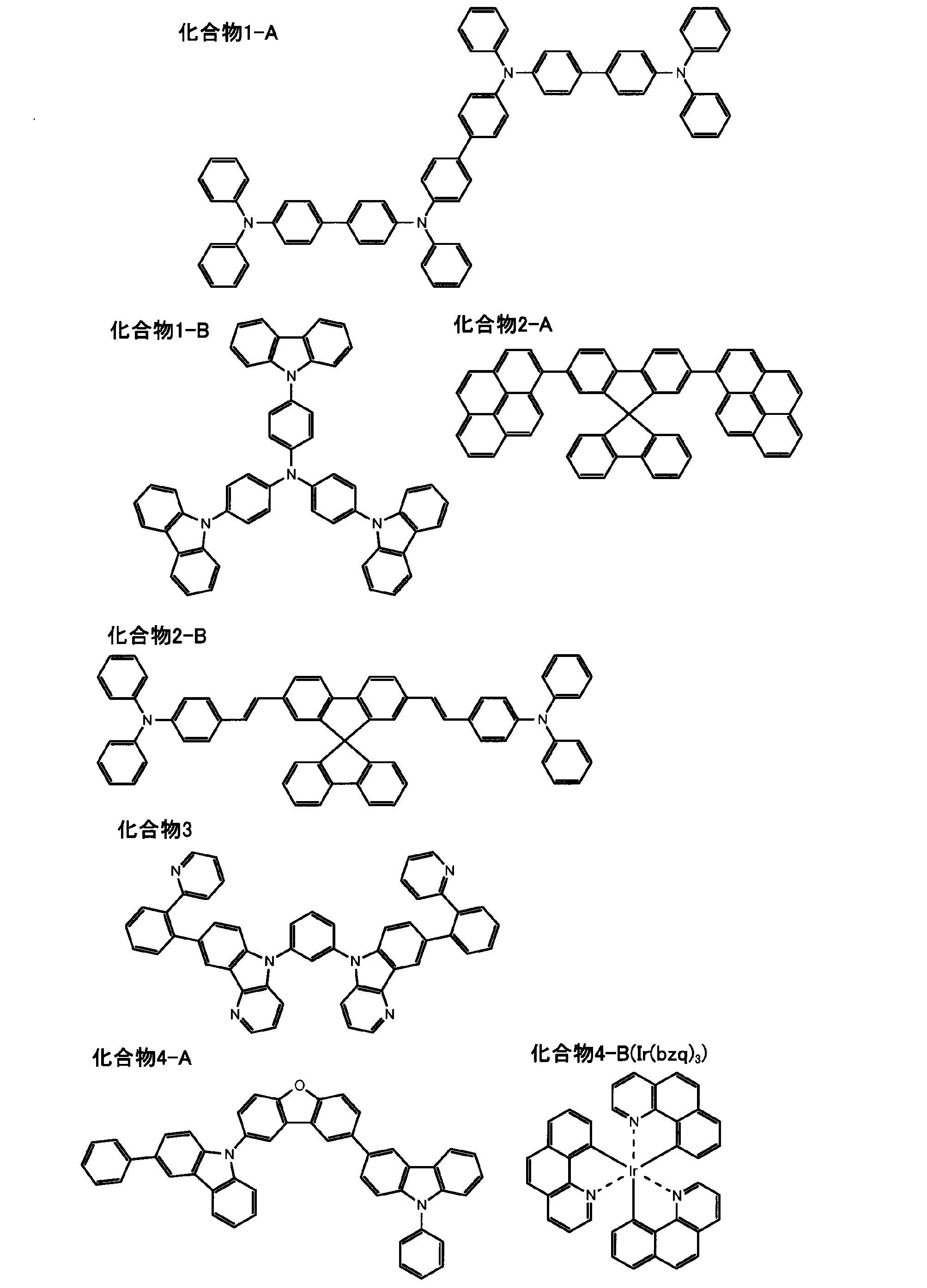
[試料102~106の有機EL素子の作製]
有機EL素子の発光ユニットの構成を、表1に示すように変更した以外は、上述の試料101と同様の方法で、試料102~106の有機EL素子を作製した。なお、試料102~106の有機EL素子における距離d1,d2,d3、及び、距離Lは、各発光ユニットの正孔輸送層の厚さを調整することにより、設計値の厚さとなるように調整した。また、試料104、及び、試料106は、第1発光ユニットを作製せずに、第3発光ユニット及び第2発光ユニット(黄色発光、15vol%黄色リン光発光ドーパント化合物4-B)のみを作製した構成である。
有機EL素子の発光ユニットの構成を、表1に示すように変更した以外は、上述の試料101と同様の方法で、試料102~106の有機EL素子を作製した。なお、試料102~106の有機EL素子における距離d1,d2,d3、及び、距離Lは、各発光ユニットの正孔輸送層の厚さを調整することにより、設計値の厚さとなるように調整した。また、試料104、及び、試料106は、第1発光ユニットを作製せずに、第3発光ユニット及び第2発光ユニット(黄色発光、15vol%黄色リン光発光ドーパント化合物4-B)のみを作製した構成である。
試料101~106の有機EL素子の発光ユニットの構成、及び、最大強度角度の設計値を表1に示す。
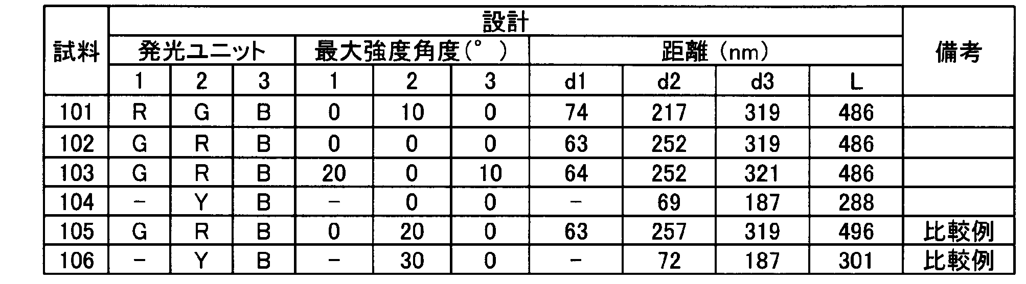
〈評価〉
[最大強度角度]
作製した有機EL素子について、室温(25℃)において電流密度が5mA/cm2となる条件下で、第1発光ユニット、第2発光ユニット、及び、第3発光ユニットを別々に発光させた。そして、空気モードの配光特性(輝度)を、光放射輝度計CS-2000を用いて、サンプル角度を-80°~0°~80°まで、5°間隔で変更して測定した。各発光ユニットの配光特性から得られる最大強度角度を下記表2に示す。
[最大強度角度]
作製した有機EL素子について、室温(25℃)において電流密度が5mA/cm2となる条件下で、第1発光ユニット、第2発光ユニット、及び、第3発光ユニットを別々に発光させた。そして、空気モードの配光特性(輝度)を、光放射輝度計CS-2000を用いて、サンプル角度を-80°~0°~80°まで、5°間隔で変更して測定した。各発光ユニットの配光特性から得られる最大強度角度を下記表2に示す。
[消費電力]
作製した有機EL素子について、室温(25℃)で各発光ユニットのピーク輝度が300cd/m2(平均輝度100cd/m2)となる条件において、PWM制御によるDUTY点灯(3ユニット時は1/3DUTY、2ユニット時は1/2DUTY)を行うときの消費電力を、分光放射輝度計CS-2000(コニカミノルタセンシング社製)を用いて測定した。
作製した有機EL素子について、室温(25℃)で各発光ユニットのピーク輝度が300cd/m2(平均輝度100cd/m2)となる条件において、PWM制御によるDUTY点灯(3ユニット時は1/3DUTY、2ユニット時は1/2DUTY)を行うときの消費電力を、分光放射輝度計CS-2000(コニカミノルタセンシング社製)を用いて測定した。
試料101~106の有機EL素子の各測定結果を表2に示す。
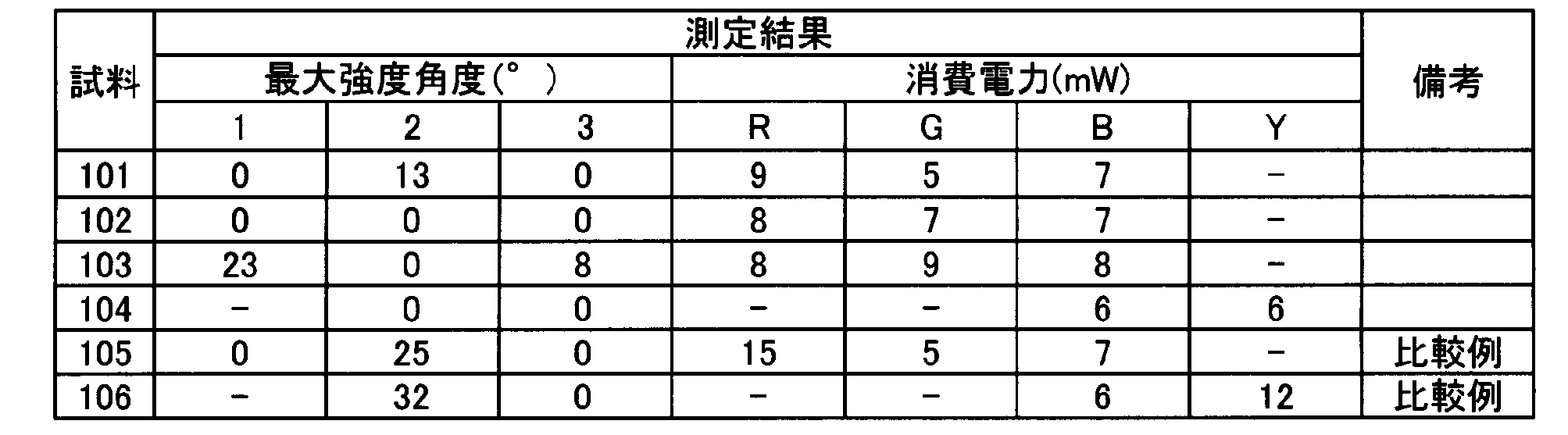
表2に示すように、発光ユニットを構成する各層の厚さを調整することにより、各試料の有機EL素子の最大強度角度において、設計値と同様の測定値が得られた。従って、上述の実施形態に記載の方法に基づく第1発光ユニットの発光点から反射電極までの距離d1、第2発光ユニットの発光点から反射電極までの距離d2、及び、第3発光ユニットの発光点から反射電極までの距離d3、並びに、透明電極から反射電極までの距離Lとなるように、有機EL素子の発光ユニットの各層の厚さを調整することにより、各発光ユニットから放出される光の最大強度角度を、所定の角度に調整することが可能となる。
試料101~104は、[θ1≦θ2]及び[θ1≦θ3]のいずれかを満たしている。このため、最も長波長の光(R又はY)を放出する発光ユニットの消費電力を、他の色(B、G)と同程度まで小さくすることができている。
一方、試料105は、第3発光ユニット(G)の最大強度角度が0°、第2発光ユニット(R)の最大強度角度が20°、第1発光ユニット(B)の最大強度角度が0°であり、[θ1≦θ2]及び[θ1≦θ3]をいずれも満たしていない。このため、長波長の光(R)の正面方向での視認性が低くなり、この光(R)を放出する第2発光ユニットの消費電力が大きくなっている。
同様に、試料106は、第2発光ユニット(Y)の最大強度角度が20°、第3発光ユニット(B)の最大強度角度が0°であり、[θ1≦θ2]を満たしていない。このため、長波長の光(Y)の正面方向での視認性が低くなり、この光(Y)を放出する第2発光ユニットの消費電力が大きくなっている。
上述のように、長波長の光の最大強度角度を小さくすることにより、正面方向での視認が向上するため、この長波長の光を放出する発光ユニットの消費電力を低減することが可能となる。従って、有機EL素子の高効率化、低消費電力化が可能となる。
なお、本発明は上述の実施形態例において説明した構成に限定されるものではなく、その他本発明構成を逸脱しない範囲において種々の変形、変更が可能である。
1・・・有機EL素子、2,11,21・・・透明電極、4,12・・・第1発光ユニット、5,7・・・電源、6・・・中間電極、8,14・・・第2発光ユニット、9・・・制御部、10,17,27・・・反射電極、13・・・第1中間電極、15・・・第2中間電極、16・・・第3発光ユニット、20・・・透明基板、22・・・発光ユニット
Claims (6)
- 2層以上の発光ユニットと、前記発光ユニットを挟持する3層以上の電極とを備える有機エレクトロルミネッセンス素子であって、
第1発光ユニットと、前記第1発光ユニットよりも波長の短い光を放出する第2発光ユニットとを有し、
正面方向から測定した、前記第1発光ユニットの発光強度が最大となる角度θ1と、前記第2発光ユニットの発光強度が最大となる角度θ2とが[θ1≦θ2 (但し、0°≦θ1≦θ2<90°)]を満たす
有機エレクトロルミネッセンス素子。 - 前記第2発光ユニットよりも波長の短い光を放出する第3発光ユニットを有し、
正面方向から測定した、前記第1発光ユニットの発光強度が最大となる角度θ1と、前記第2発光ユニットの発光強度が最大となる角度θ2と、前記第3発光ユニットの発光強度が最大となる角度θ3とが[θ1≦θ2、且つ、θ1≦θ3 (但し、0°≦θ1≦θ2<90°、0°≦θ1≦θ3<90°)]を満たす、
請求項1に記載の有機エレクトロルミネッセンス素子。 - 0°≦θ1≦5°の関係を満たす請求項1に記載の有機エレクトロルミネッセンス素子。
- 前記第1発光ユニットの[全光束/正面輝度]をP1、前記第2発光ユニットの[全光束/正面輝度]をP2としたとき、[P1≦P2]を満たす請求項1に記載の有機エレクトロルミネッセンス素子。
- 前記第2発光ユニットよりも波長の長い光を放出する第3発光ユニットを有し、前記第3発光ユニットの[全光束/正面輝度]をP3としたとき、[P1≦P2≦P3]を満たす請求項4に記載の有機エレクトロルミネッセンス素子。
- 請求項1に記載の有機エレクトロルミネッセンス素子を備える発光装置。
Priority Applications (1)
| Application Number | Priority Date | Filing Date | Title |
|---|---|---|---|
| JP2017556353A JPWO2017104175A1 (ja) | 2015-12-17 | 2016-08-23 | 有機エレクトロルミネッセンス素子、及び、発光装置 |
Applications Claiming Priority (2)
| Application Number | Priority Date | Filing Date | Title |
|---|---|---|---|
| JP2015-246639 | 2015-12-17 | ||
| JP2015246639 | 2015-12-17 |
Publications (1)
| Publication Number | Publication Date |
|---|---|
| WO2017104175A1 true WO2017104175A1 (ja) | 2017-06-22 |
Family
ID=59055916
Family Applications (1)
| Application Number | Title | Priority Date | Filing Date |
|---|---|---|---|
| PCT/JP2016/074499 Ceased WO2017104175A1 (ja) | 2015-12-17 | 2016-08-23 | 有機エレクトロルミネッセンス素子、及び、発光装置 |
Country Status (2)
| Country | Link |
|---|---|
| JP (1) | JPWO2017104175A1 (ja) |
| WO (1) | WO2017104175A1 (ja) |
Citations (4)
| Publication number | Priority date | Publication date | Assignee | Title |
|---|---|---|---|---|
| JPH09296166A (ja) * | 1996-05-02 | 1997-11-18 | Idemitsu Kosan Co Ltd | ポルフィリン誘導体を含有する有機エレクトロルミネッセンス素子 |
| JP2010015787A (ja) * | 2008-07-02 | 2010-01-21 | Canon Inc | 有機el表示装置 |
| WO2011040294A1 (ja) * | 2009-09-29 | 2011-04-07 | 住友化学株式会社 | 有機エレクトロルミネッセンス素子 |
| JP2013077383A (ja) * | 2011-09-29 | 2013-04-25 | Canon Inc | 表示装置 |
-
2016
- 2016-08-23 JP JP2017556353A patent/JPWO2017104175A1/ja active Pending
- 2016-08-23 WO PCT/JP2016/074499 patent/WO2017104175A1/ja not_active Ceased
Patent Citations (4)
| Publication number | Priority date | Publication date | Assignee | Title |
|---|---|---|---|---|
| JPH09296166A (ja) * | 1996-05-02 | 1997-11-18 | Idemitsu Kosan Co Ltd | ポルフィリン誘導体を含有する有機エレクトロルミネッセンス素子 |
| JP2010015787A (ja) * | 2008-07-02 | 2010-01-21 | Canon Inc | 有機el表示装置 |
| WO2011040294A1 (ja) * | 2009-09-29 | 2011-04-07 | 住友化学株式会社 | 有機エレクトロルミネッセンス素子 |
| JP2013077383A (ja) * | 2011-09-29 | 2013-04-25 | Canon Inc | 表示装置 |
Also Published As
| Publication number | Publication date |
|---|---|
| JPWO2017104175A1 (ja) | 2018-10-11 |
Similar Documents
| Publication | Publication Date | Title |
|---|---|---|
| JP5098645B2 (ja) | 有機エレクトロルミネッセンス素子、液晶表示装置及び照明装置 | |
| JP6337883B2 (ja) | 電子デバイス | |
| JP2007189002A (ja) | 有機エレクトロルミネッセンス素子および有機エレクトロルミネッセンスディスプレイ | |
| JP4830374B2 (ja) | 有機エレクトロルミネッセンス素子、液晶表示装置及び照明装置 | |
| JP5664715B2 (ja) | 有機エレクトロルミネッセンス素子 | |
| WO2011132550A1 (ja) | 有機エレクトロルミネッセンス素子、表示装置及び照明装置 | |
| WO2017104174A1 (ja) | 有機エレクトロルミネッセンス素子、及び、発光装置 | |
| JP2009252944A (ja) | 有機エレクトロルミネセンス素子とその製造方法 | |
| JP2007180277A (ja) | 有機エレクトロルミネッセンス素子、表示装置及び照明装置 | |
| JP2017033849A (ja) | 有機電界発光素子、有機電界発光素子の製造方法、および照明装置 | |
| JP6119606B2 (ja) | 有機エレクトロルミネッセンスパネル及び有機エレクトロルミネッセンスパネルの製造方法 | |
| JP5217844B2 (ja) | 照明用面発光パネル | |
| WO2014200067A1 (ja) | 有機エレクトロルミネッセンス素子、及び、電子機器 | |
| JP2007059118A (ja) | 有機エレクトロルミネッセンス素子、液晶表示装置及び照明装置 | |
| JP4978034B2 (ja) | 有機エレクトロルミネッセンス素子 | |
| WO2018083974A1 (ja) | 有機エレクトロルミネッセンス素子、及び、発光装置 | |
| JP2017112011A (ja) | 有機エレクトロルミネッセンス素子、及び、発光装置 | |
| JPWO2007077715A1 (ja) | ボトムエミッション型有機エレクトロルミネッセンスパネル | |
| WO2017104175A1 (ja) | 有機エレクトロルミネッセンス素子、及び、発光装置 | |
| WO2014185219A1 (ja) | 有機エレクトロルミネッセンス素子の製造方法及び有機エレクトロルミネッセンス素子 | |
| WO2018116923A1 (ja) | 透明電極及び電子デバイス | |
| JP6252590B2 (ja) | 有機エレクトロルミネッセンス素子及び有機エレクトロルミネッセンス素子の製造方法 | |
| WO2014181695A1 (ja) | 有機エレクトロルミネッセンス素子 | |
| JP5895699B2 (ja) | 有機エレクトロルミネッセンス素子 | |
| JP2007221028A (ja) | 有機エレクトロルミネッセンス素子、表示装置及び照明装置 |
Legal Events
| Date | Code | Title | Description |
|---|---|---|---|
| 121 | Ep: the epo has been informed by wipo that ep was designated in this application |
Ref document number: 16875162 Country of ref document: EP Kind code of ref document: A1 |
|
| ENP | Entry into the national phase |
Ref document number: 2017556353 Country of ref document: JP Kind code of ref document: A |
|
| NENP | Non-entry into the national phase |
Ref country code: DE |
|
| 122 | Ep: pct application non-entry in european phase |
Ref document number: 16875162 Country of ref document: EP Kind code of ref document: A1 |