WO2017090323A1 - タッチパネル用積層体 - Google Patents
タッチパネル用積層体 Download PDFInfo
- Publication number
- WO2017090323A1 WO2017090323A1 PCT/JP2016/079564 JP2016079564W WO2017090323A1 WO 2017090323 A1 WO2017090323 A1 WO 2017090323A1 JP 2016079564 W JP2016079564 W JP 2016079564W WO 2017090323 A1 WO2017090323 A1 WO 2017090323A1
- Authority
- WO
- WIPO (PCT)
- Prior art keywords
- sensor sheet
- protective film
- region
- laminate
- touch panel
- Prior art date
- Legal status (The legal status is an assumption and is not a legal conclusion. Google has not performed a legal analysis and makes no representation as to the accuracy of the status listed.)
- Ceased
Links
Images



Classifications
-
- G—PHYSICS
- G06—COMPUTING OR CALCULATING; COUNTING
- G06F—ELECTRIC DIGITAL DATA PROCESSING
- G06F3/00—Input arrangements for transferring data to be processed into a form capable of being handled by the computer; Output arrangements for transferring data from processing unit to output unit, e.g. interface arrangements
- G06F3/01—Input arrangements or combined input and output arrangements for interaction between user and computer
- G06F3/03—Arrangements for converting the position or the displacement of a member into a coded form
- G06F3/041—Digitisers, e.g. for touch screens or touch pads, characterised by the transducing means
-
- G—PHYSICS
- G06—COMPUTING OR CALCULATING; COUNTING
- G06F—ELECTRIC DIGITAL DATA PROCESSING
- G06F3/00—Input arrangements for transferring data to be processed into a form capable of being handled by the computer; Output arrangements for transferring data from processing unit to output unit, e.g. interface arrangements
- G06F3/01—Input arrangements or combined input and output arrangements for interaction between user and computer
- G06F3/03—Arrangements for converting the position or the displacement of a member into a coded form
- G06F3/041—Digitisers, e.g. for touch screens or touch pads, characterised by the transducing means
- G06F3/044—Digitisers, e.g. for touch screens or touch pads, characterised by the transducing means by capacitive means
- G06F3/0445—Digitisers, e.g. for touch screens or touch pads, characterised by the transducing means by capacitive means using two or more layers of sensing electrodes, e.g. using two layers of electrodes separated by a dielectric layer
-
- G—PHYSICS
- G06—COMPUTING OR CALCULATING; COUNTING
- G06F—ELECTRIC DIGITAL DATA PROCESSING
- G06F3/00—Input arrangements for transferring data to be processed into a form capable of being handled by the computer; Output arrangements for transferring data from processing unit to output unit, e.g. interface arrangements
- G06F3/01—Input arrangements or combined input and output arrangements for interaction between user and computer
- G06F3/03—Arrangements for converting the position or the displacement of a member into a coded form
- G06F3/041—Digitisers, e.g. for touch screens or touch pads, characterised by the transducing means
- G06F3/044—Digitisers, e.g. for touch screens or touch pads, characterised by the transducing means by capacitive means
- G06F3/0446—Digitisers, e.g. for touch screens or touch pads, characterised by the transducing means by capacitive means using a grid-like structure of electrodes in at least two directions, e.g. using row and column electrodes
Definitions
- the present invention relates to a laminate for a touch panel in which a sensor sheet having a detection electrode for detecting a touch and a protective film for protecting the sensor sheet are laminated, and in particular, the sensor sheet is thin for weight reduction and thickness reduction. It is related with the laminated body for touchscreens which provided the unevenness
- a touch panel is manufactured by bonding each member (a glass substrate, a conductive film for a touch panel, a display device, and the like) through an adhesive film such as an OCA (Optical Clear Adhesive) film.
- OCA Optical Clear Adhesive
- a laminate for a touch panel in which a protective film is bonded on both sides or one side is used so that members such as a conductive film for a touch panel are not damaged in the manufacturing process (for example, patents) Reference 1).
- the protective film is appropriately peeled off, and another member is bonded in the next step.
- An object of the present invention is to provide a laminated body for a touch panel that solves the problems based on the above-described conventional technology and suppresses unexpected peeling.
- the present invention provides a touch panel including a laminate including a sensor sheet including a substrate and a detection electrode, and a protective film that is stacked on at least one surface of the sensor sheet and protects the sensor sheet.
- the sensor sheet has a thickness of 50 ⁇ m or less
- the region where the detection electrode is provided is the first region
- the region other than the first region is the second region.
- the laminated body is provided with a concave and convex portion in the second region, and provides a laminated body for a touch panel.
- the laminate has a rectangular shape having a plurality of corners in plan view, the second region is in a peripheral portion including the corners of the laminate, and the unevenness is provided in at least one corner of the laminate. Preferably it is. It is preferable that the unevenness is provided discontinuously in dots or continuously in lines.
- a protective film is provided on one side of the sensor sheet, an adhesive layer is provided on the other side of the sensor sheet, and a release film that can be peeled off from the adhesive layer is provided on the adhesive layer. It is preferable.
- the protective film is provided on both surfaces of the sensor sheet, and the unevenness is preferably provided on one of the protective film and the sensor sheet.
- the detection electrode preferably has a mesh pattern.
- the protective film is obtained by providing an adhesive layer on a substrate, and the protective film is preferably laminated with the sensor sheet with the adhesive layer facing the sensor sheet.
- (A) It is a top view which shows the laminated body for touchscreens concerning embodiment of this invention
- (b) is a schematic diagram which shows the 1st example of arrangement
- (c) is the 2nd of arrangement
- (D) is a schematic diagram showing a third example of the arrangement of the irregularities
- (e) is a schematic diagram showing a fourth example of the arrangement of the irregularities.
- (A) is typical sectional drawing which shows the 1st example of the laminated body for touchscreens concerning embodiment of this invention
- (b) is the elements on larger scale of the 1st example of the laminated body for touchscreens
- c) is a schematic cross-sectional view showing a protective film.
- FIG. 1 It is typical sectional drawing which shows the 2nd example of the laminated body for touchscreens concerning embodiment of this invention.
- (A) is a schematic plan view which shows the sensor sheet
- (b) is a schematic plan view which shows an example of the detection electrode of the sensor sheet
- (A) is typical sectional drawing which shows the 3rd example of the laminated body for touchscreens concerning embodiment of this invention
- (b) is the state which peeled the peeling film of the 3rd example of the laminated body for touchscreens. It is a typical sectional view shown.
- (A) is typical sectional drawing which shows the 1st example of the sensor sheet of the laminated body for touchscreens of this invention
- (b) is a schematic diagram which shows the 2nd example of the sensor sheet of the laminated body for touchscreens of this invention. It is typical sectional drawing
- (c) is typical sectional drawing which shows the 3rd example of the sensor sheet
- the laminated body for touchscreens of this invention is demonstrated in detail based on suitable embodiment shown to attached drawing.
- “to” indicating a numerical range includes numerical values written on both sides.
- the range of ⁇ is a range including the numerical value ⁇ and the numerical value ⁇ , and ⁇ ⁇ ⁇ ⁇ ⁇ when expressed using mathematical symbols.
- “same” includes an error range generally allowed in the technical field.
- FIG. 1A is a plan view showing a laminated body for a touch panel according to an embodiment of the present invention
- FIG. 1B is a schematic view showing a first example of arrangement of irregularities
- FIG. 1C is an arrangement of irregularities.
- It is a schematic diagram which shows the 2nd example of this
- (d) is a schematic diagram which shows the 3rd example of arrangement
- (e) is a schematic diagram which shows the 4th example of arrangement
- Fig.2 (a) is typical sectional drawing which shows the 1st example of the laminated body for touchscreens concerning embodiment of this invention, (b) is the elements on larger scale of the 1st example of the laminated body for touchscreens.
- (C) is typical sectional drawing which shows a protective film.
- the laminated body 10 for touch panels shown to Fig.1 (a) is provided with the laminated body 12.
- the laminated body 12 has a rectangular shape having a plurality of corners, for example, four corners 13b in plan view. The configuration of the laminate 12 will be described later.
- the stacked body 12 when a region where a detection electrode described later is provided is a first region S 1 and a region other than the first region S 1 is a second region S 2 , the stacked body 12 includes a second region S 2. It irregularities 14 are provided in the region S 2.
- the second region S 2 includes a peripheral portion 13a of the laminate 12.
- the first region S 1 are, for example, those corresponding to the display area such as a liquid crystal display device panel is provided, an area capable of touch detection.
- the second region S 2 is the first region S 1 other than the region.
- the second region S 2 are those corresponding to the non-display area where no image is displayed on the liquid crystal display element or the like.
- the second region S 2 for example, located in the peripheral portion 13a including the corner portion 13b of the laminate 12, irregularities 14 are provided in at least one corner 13b of the laminate 12.
- Irregularities 14, be provided on the second region S 2, not intended to be limited to the corners 13b, may be provided in a part of the second region S 2, it is provided over the entire It may be.
- the arrangement form of the irregularities 14 is not particularly limited.
- the irregularities 14 may be provided in a discontinuous manner as shown in FIG. As shown in FIG.1 (c), the unevenness
- continuous means that the unevenness
- discontinuity means that the unevenness 14 is in an independent state with no gap between the adjacent unevenness 14 with the unevenness 14 being spaced apart.
- the laminate 12 has a protective film 18 disposed on the back surface 16 b side of the sensor sheet 16, and the sensor sheet 16 and the protective film 18 are laminated.
- Concavities and convexities 14 are provided in the second region S 2 of the stacked body 12.
- the unevenness 14 is obtained by integrally deforming the sensor sheet 16 and the protective film 18, and is different from at least one roughening of the sensor sheet 16 and the protective film 18.
- the back surface 16 b of the sensor sheet 16 corresponds to one surface of the sensor sheet 16.
- the unevenness 14 of the laminate 12 is obtained by integrally deforming the sensor sheet 16 and the protective film 18, physically improving the adhesion between the sensor sheet 16 and the protective film 18, and improving the peel strength of the laminate 12. It is. Thereby, unexpected peeling can be suppressed and it can be prevented from peeling until the timing at which peeling of the protective film 18 is necessary.
- corrugation 14 can fulfill
- corrugation 14 will not be specifically limited, One may be sufficient.
- the adhesive force of the sensor sheet 16 and the protective film 18 can be adjusted by adjusting the size, the number of arrangement, the arrangement density, and the like of the unevenness 14.
- the unevenness 14 can be formed, for example, by being deformed to such an extent that the laminated body 12 is not broken.
- corrugation 14 is not specifically limited, The unevenness
- the thickness of the sensor sheet 16 is d, and the maximum height of the irregularities 14 is h.
- the thickness d of the sensor sheet 16 is 50 ⁇ m or less.
- the thickness d of the sensor sheet 16 and the maximum height h of the irregularities 14 are preferably h / d> 1.2.
- the sensor sheet 16 includes, as detection electrodes, a first detection unit 32 (see FIG. 4A) composed of conductive thin wires 36 (see FIG. 4B) and a plurality of second detection units 34 (see FIG. 4). 4 (a)), the maximum height h of the irregularities 14 is preferably higher than the height of the detection electrodes. Thereby, the above-mentioned function can be exhibited reliably.
- the height of the detection electrode is a thickness t (see FIG. 6A) of a conductive thin wire 36 to be described later, and the thickness d of the sensor sheet 16 will be described in detail later.
- the protective film 18 protects the sensor sheet 16, and prevents the sensor sheet 16 from rubbing.
- the protective film 18 protects the detection electrode, for example.
- the protective film 18 is peeled off when the sensor sheet 16 is attached to, for example, a liquid crystal display device, and the protective film 18 is finally peeled off from the sensor sheet 16.
- the protective film 18 is one in which an adhesive layer 42 is provided on a base material 40.
- the protective film 18 is laminated with the sensor sheet 16 with the adhesive layer 42 facing the back surface 16 b of the sensor sheet 16. By making the base material 40 and the adhesive layer 42 optically transparent in the protective film 18, the sensor sheet 16 can be visually recognized.
- the base material 40 and the adhesive layer 42 of the protective film 18 will be described in detail later.
- corrugated force 14 is provided in 2nd area
- the adhesive force of the sensor sheet 16 and the protective film 18 improves, the peeling strength of the interface B increases, and the sensor sheet 16 and the protective film 18 becomes difficult to peel off.
- the thickness of the sensor sheet 16 is as thin as 50 ⁇ m or less
- unexpected peeling at the interface B between the protective film 18 and the sensor sheet 16 is suppressed when an external force is applied to the touch panel laminate 10. can do.
- the unevenness 14 the adhesion between the protective film 18 and the sensor sheet 16 can be improved, the unexpected peeling can be suppressed, and the protective film 18 can be prevented from being peeled off until the peeling is necessary.
- the laminate 12 is not limited to the configuration shown in FIG. 2A, and may be, for example, the laminate 20 of the touch panel laminate 10a shown in FIG.
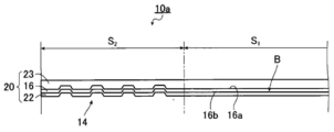
- FIG. 3 is a schematic cross-sectional view showing a second example of the laminate for a touch panel according to the embodiment of the present invention.
- the same components as those in the touch panel laminate 10 shown in FIG. 2A are denoted by the same reference numerals, and detailed description thereof is omitted.
- seat 16, and provided the 2nd protective film 23 in the surface 16a may be sufficient.
- the unevenness 14 is provided on the first protective film 22 and the sensor sheet 16, or the sensor sheet 16 and the second protective film 23.
- the first protective film 22 and the second protective film 23 have the same configuration as the protective film 18 described above. For this reason, the detailed description is abbreviate
- the structure of the laminate 20 shown in FIG. 3 can also exhibit the same function as the laminate 12 described above.
- the sensor sheet 16 and the second protective film 23 in order to suppress unexpected peeling, the sensor sheet 16, between the first protective film 22 and the sensor sheet 16. It is necessary to change the adhesion, that is, the peel strength between the protective film 23 and the second protective film 23. In this case, it peels off from a protective film with comparatively small adhesive force.
- the back surface 16 b of the sensor sheet 16 corresponds to one surface of the sensor sheet 16, and the front surface 16 a corresponds to the other surface of the sensor sheet 16.
- FIG. 4A is a schematic plan view showing a sensor sheet of the touch panel laminate
- FIG. 4B is a schematic plan view showing an example of a detection electrode of the sensor sheet of the touch panel laminate.
- the sensor sheet 16 used for the laminate 12 is formed on the substrate 30, the detection electrodes formed on both surfaces of the substrate 30, and the detection electrodes, respectively. And peripheral wiring electrically connected.
- the sensor sheet 16 is, for example, a capacitive touch sensor. More specifically, a plurality of first detections each extending along the first direction Y on the surface 30a of the substrate 30 and arranged in parallel in a second direction X orthogonal to the first direction Y.
- a portion 32 is formed, and a plurality of first peripheral wirings 33 electrically connected to the plurality of first detection portions 32 are arranged close to each other.
- a plurality of second detectors 34 that extend along the second direction X and are arranged in parallel in the first direction Y are formed, and a plurality of second detectors 34 are formed.
- a plurality of second peripheral wirings 35 that are electrically connected to the detector 34 are arranged close to each other.
- the first detection unit 32 and the plurality of second detection units 34 are detection electrodes.
- a region in the substrate 30 where the plurality of first detection units 32 and the plurality of second detection units 34 are overlapped in plan view is a sensor region 37.
- the sensor region 37 is a region where a touch can be detected in the capacitive touch sensor.
- the sensor area 37 of the sensor sheet 16 shown in FIG. 4 (a) corresponds to the first region S 1 described above, it areas peripheral wiring and the like are provided other than corresponds to the second region S 2.
- the first detection unit 32 is formed by a mesh pattern made of conductive thin wires 36
- the second detection unit 34 is also made of a mesh made of conductive thin wires 36. It is formed by a pattern.
- the mesh pattern will be described later in detail.
- the first peripheral wiring 33 and the second peripheral wiring 35 may be formed by a conductive thin wire 36, or may be configured by a conductive wiring having a line width, a thickness, etc. different from the conductive thin wire 36.
- the first peripheral wiring 33 and the second peripheral wiring 35 may be formed of, for example, a strip-shaped conductor. Each component of the sensor sheet 16 will be described in detail later.
- the sensor sheet 16 is not limited to a capacitive touch sensor, and may be a resistive film touch sensor. Even in the resistive touch sensor, a sensor region 37 is a region where the plurality of first detection units 32 and the plurality of second detection units 34 are arranged to overlap each other in plan view.
- the sensor sheet 16 is provided with the first detection unit 32, the first peripheral wiring 33, the second detection unit 34, and the second peripheral wiring 35 as described above. As a result, a region where the sensor sheet 16 and the protective film 18 are not in local contact may occur. In this case, the sensor sheet 16 and the protective film 18 are in a state where they are easily peeled off locally. In this state, even if force is applied to the interface B and the separation between the sensor sheet 16 and the protective film 18 proceeds, the unevenness 14 becomes a separation barrier, and the extension of the separation between the sensor sheet 16 and the protective film 18 is suppressed.
- Fig.5 (a) is typical sectional drawing which shows the 3rd example of the laminated body for touchscreens concerning embodiment of this invention, (b) peeled off the peeling film of the 3rd example of the laminated body for touchscreens. It is typical sectional drawing which shows a state. 5A and 5B, the same components as those in the touch panel laminate 10 shown in FIG. 2A are denoted by the same reference numerals, and detailed description thereof is omitted.
- the laminated body 10b for a touch panel shown in FIG. 5A has an adhesive on the surface 16a of the sensor sheet 16 as compared with the laminated body 12 of the laminated body 10 for a touch panel shown in FIG.
- the layer 26 is provided and the release film 28 is provided on the surface 26a of the pressure-sensitive adhesive layer 26.
- the other configuration is the same as that of the laminate 12 of the touch panel laminate 10 shown in FIG. Since it is a structure, the detailed description is abbreviate
- the pressure-sensitive adhesive layer 26 is for bonding the touch panel laminate 10b to another member.
- an optically transparent adhesive OCA, Optical Clear Resin
- OCA optically transparent adhesive
- UV Ultra Violet
- both optically transparent and simply transparent means that the light transmittance is at least 60% or more, preferably 75% or more, more preferably in the visible light wavelength range of 400 to 800 nm. 80% or more, still more preferably 85% or more.
- the light transmittance is measured using, for example, “Plastic—How to obtain total light transmittance and total light reflectance” defined in JIS K 7375: 2008.
- the release film 28 protects the pressure-sensitive adhesive layer 26 and can be removed when the pressure-sensitive adhesive layer 26 is used.
- the release film 28 is provided on the surface 26 a of the pressure-sensitive adhesive layer 26 so as to be peelable from the pressure-sensitive adhesive layer 26. When the release film 28 is peeled from the pressure-sensitive adhesive layer 26, it is preferable that even a part of the release film 28 does not remain in the pressure-sensitive adhesive layer 26.
- the release film 28 is made of, for example, a silicone resin or a fluorine resin. The description of the release film 28 will be omitted later.
- Touch panel laminate 10b shown in FIG. 5 (a) is peeled off the release film 28, but another member is attached to the surface 26a of the adhesive layer 26, the provision of the second region S 2 on the uneven 14
- peeling at the interface B between the sensor sheet 16 and the protective film 18 is suppressed. Since the adhesion between the sensor sheet 16 and the protective film 18, that is, the peel strength, is physically improved by the unevenness 14, there is no need to increase the adhesion of the adhesive of the protective film 18, and the adhesion of the protective film 18 The agent is not transferred to the sensor sheet 16.
- FIG. 6A is a schematic cross-sectional view showing a first example of the sensor sheet of the laminate for a touch panel of the present invention
- FIG. 6B shows a second example of the sensor sheet of the laminate for a touch panel of the present invention. It is a typical sectional view shown
- (c) is a typical sectional view showing the 3rd example of the sensor sheet of the layered product for touch panels of the present invention.
- the sensor sheet 16 has a first detection unit 32 formed on the front surface 30 a of the substrate 30 and a second detection unit 34 formed on the back surface 30 b of the substrate 30.
- the first detection unit 32 and the second detection unit 34 are configured by conductive thin wires 36.
- the thickness d of the sensor sheet 16 shown in FIG. 6A is the distance between the surface 36 a of the conductive thin wire 36 of the first detection unit 32 and the surface 36 a of the conductive thin wire 36 of the second detection unit 34.
- the first detection unit 32 is formed on the front surface 30 a of one substrate 30, and the second detection unit 34 is formed on the front surface 31 a via the adhesive layer 38 on the back surface 30 b of the substrate 30.
- stacked may be sufficient.
- the substrate 31 has the same configuration as the substrate 30.
- the thickness d of the sensor sheet 16 shown in FIG. 6B is the distance between the surface 36 a of the conductive thin wire 36 of the first detection unit 32 and the back surface 31 b of the substrate 31.
- the sensor sheet 16 is provided with two detection units, but is not limited to this.
- a configuration in which the first detection unit 32 is provided on the surface 30 a of one substrate 30 may be used.
- the thickness d of the sensor sheet 16 shown in FIG. 6C is the distance between the surface 36 a of the conductive thin wire 36 of the first detection unit 32 and the back surface 30 b of the substrate 30.
- a cross-sectional image of the sensor sheet 16 including the conductive thin wires 36 is acquired, the cross-sectional image is captured on a personal computer, displayed on the monitor, and the thickness d of the sensor sheet 16 described above on the monitor.
- the horizontal line is drawn at each of the two locations that define the distance between the horizontal lines. Thereby, the thickness d of the sensor sheet 16 can be obtained.
- the line width w of the conductive thin wire 36 and the thickness t of the conductive thin wire 36 can be measured using the cross-sectional image of the sensor sheet 16 in the same manner as the thickness d of the sensor sheet 16 described above.
- the type of the substrate is not particularly limited as long as it can support the first detection unit, the first peripheral wiring, the second detection unit, and the second peripheral wiring, but is a transparent base material.
- a plastic film is preferable.
- the material constituting the substrate include PET (polyethylene terephthalate) (258 ° C.), polycycloolefin (134 ° C.), polycarbonate (250 ° C.), acrylic resin (128 ° C.), PEN (polyethylene naphthalate) (269 ° C), PE (polyethylene) (135 ° C), PP (polypropylene) (163 ° C), polystyrene (230 ° C), polyvinyl chloride (180 ° C), polyvinylidene chloride (212 ° C) and TAC (triacetylcellulose) ( 290 ° C.) or the like, and a plastic film having a melting point of about 290 ° C. or less is preferable, and PET, polycycloolefin, and polycarbonate are particularly preferable.
- Figures in parentheses are melting points.
- the total light transmittance of the substrate is preferably 85% to 100%.
- the total light transmittance is measured using, for example, “Plastic—How to obtain total light transmittance and total light reflectance” defined in JIS K 7375: 2008.
- the thickness of the substrate is selected so that the thickness d of the sensor sheet is 50 ⁇ m or less.
- the thickness of the substrate is preferably 5 to 40 ⁇ m, and most preferably 10 to 30 ⁇ m.
- One preferred embodiment of the substrate is a treated substrate that has been subjected to at least one treatment selected from the group consisting of atmospheric pressure plasma treatment, corona discharge treatment, and ultraviolet irradiation treatment.
- a hydrophilic group such as an OH group is introduced into the surface of the processed substrate, and the first detection unit, the first peripheral wiring, the second detection unit, and the second detection unit
- the adhesion of the peripheral wiring to the substrate is further improved.
- the atmospheric pressure plasma process is preferable in that the adhesion of the first detection unit, the first peripheral wiring, the second detection unit, and the second peripheral wiring to the substrate is further improved.
- an undercoat layer containing a polymer on a surface on which the first detection unit, the first peripheral wiring, the second detection unit, and the second peripheral wiring are provided.
- a first detection unit, a first peripheral wiring, a second detection unit, and a photosensitive layer for forming a second peripheral wiring are formed, whereby the first detection unit is formed.
- the adhesion of the first peripheral wiring, the second detection unit, and the second peripheral wiring to the substrate is further improved.
- a method for forming the undercoat layer is not particularly limited, and examples thereof include a method in which a composition for forming an undercoat layer containing a polymer is applied on a substrate and heat-treated as necessary.
- the undercoat layer forming composition may contain a solvent, if necessary.
- the kind of solvent is not specifically limited, The solvent used with the composition for photosensitive layer formation mentioned later is illustrated.
- latex containing polymer fine particles may be used as the composition for forming an undercoat layer containing polymer.
- the thickness of the undercoat layer is not particularly limited, in that the adhesion of the first detection unit, the first peripheral wiring, the second detection unit, and the second peripheral wiring to the substrate is more excellent, 0.02 to 0.3 ⁇ m is preferable, and 0.03 to 0.2 ⁇ m is more preferable.
- the conductive thin wire has electrical conductivity, and is made of, for example, a metal, an alloy, and a metal oxide such as ITO (Indium Tin Oxide) and ZnO.
- the conductive thin wire is formed by, for example, a sputtering method or a vapor deposition method.
- the conductive thin wire can be formed by, for example, forming a metal layer by a vapor deposition method and patterning it using a photolithography method.
- the conductive thin wire is composed of a metal thin wire, for example, it can be composed of a copper wire or a silver wire.
- the metal thin wire preferably contains metallic silver, but may contain metals other than metallic silver, such as gold and copper.
- the fine metal wire contains a polymer binder such as metal silver and gelatin.
- the conductive thin wire is not limited to the above-described metal, alloy, or metal oxide, and for example, metal oxide particles, metal paste such as silver paste and copper paste, and silver nanowires and It may contain metal nanowire particles such as copper nanowires.
- a mesh pattern can also be formed by a conductive thin wire.
- the conductive fine wire is preferably a metal fine wire, an alloy fine wire and a metal oxide thin film, particularly preferably a metal fine wire, which contains a polymer binder such as the above-mentioned metal silver and gelatin. More preferably it is.
- the line width w of the conductive thin wire is not particularly limited, but is preferably 30 ⁇ m or less, more preferably 15 ⁇ m or less, further preferably 10 ⁇ m or less, particularly preferably 9 ⁇ m or less, 7 ⁇ m or less is most preferable, 0.5 ⁇ m or more is preferable, and 1.0 ⁇ m or more is more preferable. If the line width w is in the above range, a low-resistance detection electrode can be formed relatively easily.
- the line width w of the conductive thin wire is preferably 500 ⁇ m or less, more preferably 50 ⁇ m or less, and particularly preferably 30 ⁇ m or less. If the line width w is in the above range, a low resistance peripheral wiring can be formed relatively easily.
- the peripheral wiring in the sensor sheet can also be a mesh pattern as in the detection electrode.
- w is not particularly limited, but is preferably 30 ⁇ m or less, more preferably 15 ⁇ m or less, further preferably 10 ⁇ m or less, particularly preferably 9 ⁇ m or less, most preferably 7 ⁇ m or less, preferably 0.5 ⁇ m or more, 1.0 ⁇ m The above is more preferable. If the line width w is in the above range, a low resistance peripheral wiring can be formed relatively easily.
- the peripheral wiring on the sensor sheet as a mesh pattern, when forming the detection electrode, in the process of irradiating the pulsed light from the xenon flash lamp, the uniformity of low resistance by irradiation of the detection electrode and the peripheral wiring is improved.
- the adhesive layer when the adhesive layer is bonded, it is preferable in that the peel strength between the detection electrode and the peripheral wiring can be made constant and the in-plane distribution can be reduced.
- the thickness t of the conductive thin wire is not particularly limited, but is preferably 1 to 200 ⁇ m, more preferably 30 ⁇ m or less, and further preferably 20 ⁇ m or less, The thickness is particularly preferably from 0.01 to 9 ⁇ m, and most preferably from 0.05 to 5 ⁇ m. When the thickness t is in the above range, a detection electrode having low resistance and excellent durability can be formed relatively easily.
- the pattern of the detection electrode is not particularly limited, but is a triangle such as a regular triangle, an isosceles triangle, a right triangle, a square, a rectangle, a rhombus, a parallelogram, a trapezoid, or a quadrangle, a (positive) hexagon, ( It is preferably a geometric figure combining (positive) n-gons such as (positive) octagons, circles, ellipses, stars, etc., and more preferably a mesh pattern composed of these geometric figures.
- the mesh pattern is a combination of a large number of cells configured in a lattice shape with thin conductive wires. Specifically, as shown in FIG.
- the mesh pattern may be a combination of similar and congruent grids, or may be a combination of differently shaped grids.
- the conductive film may include, for example, an antihalation layer other than the above-described undercoat layer as another layer between the base material and the conductive portion.
- an antihalation layer other than the above-described undercoat layer as another layer between the base material and the conductive portion.
- the sensor sheet When the sensor sheet has peripheral wiring, the sensor sheet preferably has an insulating film that covers at least a part of the peripheral wiring. That is, it is preferable that an insulating film covering a part of the second region S 2.
- the insulating film is not particularly limited, but preferably a UV (Ultra Violet) curable insulating resin applied and cured by UV light, a thermosetting insulating resin applied and cured by heat, In particular, a resin that is coated with a UV curable insulating resin and cured by UV light is preferable.
- the width and thickness of the insulating film, the second region S 2 of the size of the sensor sheet, is to be determined appropriately according to the thickness or the like of the peripheral wiring.
- the thickness d of the sensor sheet is the thickness of the thickest part including the insulating film.
- a film whose surface is treated with a silicone-based release agent or other release agent, a film that itself has release properties, a film in which an adhesion layer is formed on a support, and the like can be used.
- the material which comprises a film and a support body is not specifically limited, For example, the material illustrated by the above-mentioned board
- adherence layer is the same as the adhesive as described in the below-mentioned adhesive layer.
- the thickness of the release film is not particularly limited, but is preferably 50 to 200 ⁇ m, more preferably 75 to 125 ⁇ m.
- the release film 28 is, for example, a film obtained by treating the above-described surface with a silicone release agent or other release agent.
- the support include polyester such as polyethylene terephthalate (PET) and polyethylene naphthalate (PEN), polycarbonate (PC), polymethyl methacrylate (PMMA), cycloolefin polymer (COP), triacetyl cellulose (TAC), poly Arylate (PAR), polysulfone (PSU), polystyrene (PS) and the like can be used.
- the acrylic pressure-sensitive adhesive is preferably mainly composed of an acrylic polymer having a repeating unit derived from an alkyl (meth) acrylate.
- (Meth) acrylate refers to acrylate and / or methacrylate.
- the acrylic polymer is preferably an acrylic polymer having a repeating unit derived from an alkyl (meth) acrylate having an alkyl group having about 1 to 12 carbon atoms.
- the thickness of the pressure-sensitive adhesive layer is not particularly limited, but is preferably 25 to 300 ⁇ m, and more preferably 50 to 200 ⁇ m.
- the same substrate as the release film support can be used.
- the thing similar to the adhesion layer of the above-mentioned peeling film can be used for the adhesion layer of a protective film.
- the present invention is basically configured as described above. As mentioned above, although the laminated body for touchscreens of this invention was demonstrated in detail, this invention is not limited to the above-mentioned embodiment, In the range which does not deviate from the main point of this invention, what may be variously improved or changed. Of course.
Landscapes
- Engineering & Computer Science (AREA)
- General Engineering & Computer Science (AREA)
- Theoretical Computer Science (AREA)
- Human Computer Interaction (AREA)
- Physics & Mathematics (AREA)
- General Physics & Mathematics (AREA)
- Laminated Bodies (AREA)
Abstract
予期せぬ剥離を抑制するタッチパネル用積層体を提供する。タッチパネル用積層体は、基板および検出電極を備えるセンサーシートと、センサーシートの少なくとも一方の面に積層された、センサーシートを保護する保護フィルムとを有する積層体を備える。タッチパネル用積層体は、センサーシートは厚みが50μm以下である。積層体では、検出電極が設けられた領域を第1の領域とし、第1の領域以外の領域を第2の領域とするとき、積層体には第2の領域に凹凸が設けられている。
Description
本発明は、タッチを検出する検出電極を有するセンサーシートと、このセンサーシートを保護する保護フィルムが積層されたタッチパネル用積層体に関し、特に、軽量化および薄型化のためにセンサーシート厚みが薄く、センサーシートと保護フィルムの積層体に一体に凹凸を設けたタッチパネル用積層体に関する。
近年、タブレット型コンピュータおよびスマートフォン等の携帯情報機器を始めとした各種の電子機器において、液晶表示装置等の表示装置と組み合わせて用いられ、画面に接触することにより電子機器への入力操作を行うタッチパネルの普及が進んでいる。
一般に、タッチパネルは、各部材(ガラス基板、タッチパネル用導電フィルム、表示装置等)をOCA(Optical Clear Adhesive)フィルム等の粘着フィルムを介して貼り合わせることによって製造されている。通常、タッチパネルの製造では、製造工程にてタッチパネル用導電フィルム等の部材に傷が付かないように、両面または片面に保護フィルムが貼り合わせられたタッチパネル用積層体が用いられている(例えば、特許文献1)。保護フィルムは適宜剥離され、次の工程にて別の部材が貼り合される。
現在、タブレット型コンピュータおよびスマートフォン等では軽量化および薄型化が求められており、タッチパネルの薄型化の検討が盛んに行われている。近年、導入が進んでいるフィルムタイプのセンサーシートを有するタッチパネルにおいても薄型化の検討が盛んに行われている。
しかし、タッチパネルは、ハンドリングによりクニックまたは折れが発生するため保護フィルムを付けてハンドリングする必要がある。また、使用する保護フィルムは使い捨てのため、なるべく薄くし材料コストを下げる検討が進んでいる。
上述の特許文献1のように、保護フィルムが貼り合わせられたタッチパネルが提案されているが、センサーシートの薄型化と保護フィルムの薄型化に伴い、外力が加わった際に保護フィルムとセンサーシートの界面に予期せぬ剥離が起きるという問題がある。この予期せぬ剥離を防止しようとして保護フィルムの粘着剤(Adhesive)を改良し密着力を上げようとすると保護フィルムの粘着剤がセンサーシートに転写してしまうという問題がある。
しかし、タッチパネルは、ハンドリングによりクニックまたは折れが発生するため保護フィルムを付けてハンドリングする必要がある。また、使用する保護フィルムは使い捨てのため、なるべく薄くし材料コストを下げる検討が進んでいる。
上述の特許文献1のように、保護フィルムが貼り合わせられたタッチパネルが提案されているが、センサーシートの薄型化と保護フィルムの薄型化に伴い、外力が加わった際に保護フィルムとセンサーシートの界面に予期せぬ剥離が起きるという問題がある。この予期せぬ剥離を防止しようとして保護フィルムの粘着剤(Adhesive)を改良し密着力を上げようとすると保護フィルムの粘着剤がセンサーシートに転写してしまうという問題がある。
本発明の目的は、前述の従来技術に基づく問題点を解消し、予期せぬ剥離を抑制するタッチパネル用積層体を提供することにある。
上述の目的を達成するために、本発明は、基板および検出電極を備えるセンサーシートと、センサーシートの少なくとも一方の面に積層された、センサーシートを保護する保護フィルムとを有する積層体を備えるタッチパネル用積層体であって、センサーシートは厚みが50μm以下であり、積層体において、検出電極が設けられた領域を第1の領域とし、第1の領域以外の領域を第2の領域とするとき、積層体には第2の領域に凹凸が設けられていることを特徴とするタッチパネル用積層体を提供するものである。
積層体は、平面視、複数の角部を有する矩形状であり、第2の領域は積層体の角部を含む周辺部にあり、凹凸は、積層体の少なくとも1つの角部に設けられていることが好ましい。凹凸は、点状に不連続に、または線状に連続に設けられていることが好ましい。
保護フィルムがセンサーシートの一方の面に設けられており、センサーシートの他方の面上に粘着剤層が設けられ、粘着剤層上に、粘着剤層に対して剥離可能な剥離フィルムが設けられていることが好ましい。
保護フィルムがセンサーシートの一方の面に設けられており、センサーシートの他方の面上に粘着剤層が設けられ、粘着剤層上に、粘着剤層に対して剥離可能な剥離フィルムが設けられていることが好ましい。
保護フィルムは、センサーシートの両面に設けられており、凹凸は、一方の保護フィルムとセンサーシートに設けられていることが好ましい。
検出電極は、メッシュパターンを有することが好ましい。
保護フィルムは、基材上に粘着層が設けられたものであり、保護フィルムは、粘着層をセンサーシートに向けて、センサーシートと積層されていることが好ましい。
検出電極は、メッシュパターンを有することが好ましい。
保護フィルムは、基材上に粘着層が設けられたものであり、保護フィルムは、粘着層をセンサーシートに向けて、センサーシートと積層されていることが好ましい。
本発明によれば、予期せぬ剥離を抑制することができる。
以下に、添付の図面に示す好適実施形態に基づいて、本発明のタッチパネル用積層体を詳細に説明する。
なお、以下において数値範囲を示す「~」とは両側に記載された数値を含む。例えば、εが数値α~数値βとは、εの範囲は数値αと数値βを含む範囲であり、数学記号を用いて示せばα≦ε≦βである。
また、「同一」とは、技術分野で一般的に許容される誤差範囲を含むものとする。
なお、以下において数値範囲を示す「~」とは両側に記載された数値を含む。例えば、εが数値α~数値βとは、εの範囲は数値αと数値βを含む範囲であり、数学記号を用いて示せばα≦ε≦βである。
また、「同一」とは、技術分野で一般的に許容される誤差範囲を含むものとする。
図1(a)は本発明の実施形態に係るタッチパネル用積層体を示す平面図であり、(b)は凹凸の配置の第1の例を示す模式図であり、(c)は凹凸の配置の第2の例を示す模式図であり、(d)は凹凸の配置の第3の例を示す模式図であり、(e)は凹凸の配置の第4の例を示す模式図である。図2(a)は本発明の実施形態に係るタッチパネル用積層体の第1の例を示す模式的断面図であり、(b)はタッチパネル用積層体の第1の例の部分拡大図であり、(c)は保護フィルムを示す模式的断面図である。
図1(a)に示すタッチパネル用積層体10は積層体12を備える。積層体12は、平面視、複数の角部、例えば、4つの角部13bを有する矩形状である。積層体12の構成については後に説明する。
積層体12において、後述する検出電極が設けられた領域を第1の領域S1とし、第1の領域S1以外の領域を第2の領域S2とするとき、積層体12には第2の領域S2に凹凸14が設けられている。第2の領域S2は積層体12の周辺部13aを含む。
積層体12において、後述する検出電極が設けられた領域を第1の領域S1とし、第1の領域S1以外の領域を第2の領域S2とするとき、積層体12には第2の領域S2に凹凸14が設けられている。第2の領域S2は積層体12の周辺部13aを含む。
第1の領域S1は、例えば、タッチパネルが設けられる液晶表示素子等の表示領域に対応するものであり、タッチの検出が可能な領域である。第2の領域S2は、第1の領域S1以外の領域である。第2の領域S2は、液晶表示素子等で画像が表示されない非表示領域に対応するものである。第2の領域S2は、例えば、積層体12の角部13bを含む周辺部13aにあり、凹凸14は積層体12の少なくとも1つの角部13bに設けられている。凹凸14は、第2の領域S2に設けられていれば、角部13bに特に限定されるものでなく、第2の領域S2の一部に設けられていてもよく、全域に設けられていてもよい。
凹凸14の配置形態は、特に限定されるものではない。例えば、凹凸14は、図1(b)に示すように点状に分散して不連続に設けてもよい。図1(c)に示すように凹凸14は線状に連続して設けてもよい。図1(d)に示すように凹凸14は屈曲した線状に設けてもよい。図1(e)に示すように凹凸14は、三角形の領域内に点状に分散して不連続に設けてもよい。ここで、連続とは、凹凸14が間をあけることなく隣接して配置されることをいう。不連続とは、凹凸14が間をあけて各凹凸14が隣接した凹凸14と接することなく独立した状態にあることをいう。
積層体12は、図2(a)に示すように、センサーシート16の裏面16b側に保護フィルム18が配置され、センサーシート16と保護フィルム18とが積層されたものである。積層体12の第2の領域S2に凹凸14が設けられている。凹凸14は、センサーシート16と保護フィルム18を一体に変形させたものであり、センサーシート16および保護フィルム18のうち、少なくとも一方の粗面化とは異なる。なお、センサーシート16の裏面16bがセンサーシート16の一方の面に相当する。
積層体12の凹凸14は、センサーシート16と保護フィルム18を一体に変形させており、センサーシート16と保護フィルム18の密着力を物理的に向上させ、積層体12の剥離強度を向上させるものである。これにより、予期しない剥離を抑制することができ、保護フィルム18の剥離が必要なタイミングまで剥がれないようにすることができる。
なお、凹凸14は、予期しない剥離を抑制するという機能を果たすことができれば、凹凸14の大きさ、配置数および配置密度等は、特に限定されるものではなく、1つでもよい。また、凹凸14の大きさ、配置数および配置密度等を調整することによって、センサーシート16と保護フィルム18の密着力を調整することができる。
凹凸14は、例えば、積層体12が破れない程度に変形させて形成することができ、例えば、数十μm、センサーシート16の厚み方向に変形させる。凹凸14の形成方法は、特に限定されるものではないが、凹凸14は、例えば、ナーリング加工により形成される。
なお、凹凸14は、予期しない剥離を抑制するという機能を果たすことができれば、凹凸14の大きさ、配置数および配置密度等は、特に限定されるものではなく、1つでもよい。また、凹凸14の大きさ、配置数および配置密度等を調整することによって、センサーシート16と保護フィルム18の密着力を調整することができる。
凹凸14は、例えば、積層体12が破れない程度に変形させて形成することができ、例えば、数十μm、センサーシート16の厚み方向に変形させる。凹凸14の形成方法は、特に限定されるものではないが、凹凸14は、例えば、ナーリング加工により形成される。
図2(b)に示すようにセンサーシート16の厚みをdとし、凹凸14の最大高さをhとする。このとき、センサーシート16の厚みdは50μm以下である。センサーシート16の厚みdと凹凸14の最大高さhは、h/d>1.2であることが好ましい。センサーシート16には検出電極として、導電性細線36(図4(b)参照)により構成される第1の検出部32(図4(a)参照)と複数の第2の検出部34(図4(a)参照)が設けられるが、凹凸14の最大高さhは検出電極の高さよりも高いことが好ましい。これにより、確実に上述の機能を発揮することができる。なお、検出電極の高さは、後述の導電性細線36の厚みt(図6(a)参照)のことであり、センサーシート16の厚みdについては後に詳細に説明する。
保護フィルム18は、センサーシート16を保護するものであり、センサーシート16の擦れ等を防ぐ、保護フィルム18は、例えば、検出電極を保護するものである。しかし、保護フィルム18は、センサーシート16を、例えば、液晶表示装置に貼り付ける際に剥されるものであり、保護フィルム18は、最終的にはセンサーシート16から剥されてしまうものである。
図2(c)に示すように保護フィルム18は、基材40上に粘着層42が設けられたものである。保護フィルム18は、粘着層42をセンサーシート16の裏面16bに向けて、センサーシート16と積層されている。保護フィルム18において基材40および粘着層42を光学的に透明なものとすることによって、センサーシート16を視認することができる。なお、保護フィルム18の基材40および粘着層42については、後に詳細に説明する。
図2(c)に示すように保護フィルム18は、基材40上に粘着層42が設けられたものである。保護フィルム18は、粘着層42をセンサーシート16の裏面16bに向けて、センサーシート16と積層されている。保護フィルム18において基材40および粘着層42を光学的に透明なものとすることによって、センサーシート16を視認することができる。なお、保護フィルム18の基材40および粘着層42については、後に詳細に説明する。
タッチパネル用積層体10では、第2の領域S2に凹凸14を設けることによって、センサーシート16と保護フィルム18の密着力が向上して、界面Bの剥離強度が増し、センサーシート16と保護フィルム18とが剥離しにくくなる。これにより、センサーシート16の厚さが50μm以下と薄い場合であっても、タッチパネル用積層体10に外力が加わった際に保護フィルム18とセンサーシート16の界面Bでの予期せぬ剥離を抑制することができる。このように、凹凸14を設けることによって保護フィルム18とセンサーシート16の密着性を良化し、予期せぬ剥離を抑制し、保護フィルム18の剥離が必要なタイミングまで剥がれないようにすることができる。
積層体12は、図2(a)に示す構成に限定されるものではなく、例えば、図3に示すタッチパネル用積層体10aの積層体20でもよい。
ここで、図3は本発明の実施形態に係るタッチパネル用積層体の第2の例を示す模式的断面図である。図3において図2(a)に示すタッチパネル用積層体10と同一構成物には、同一符号を付して、その詳細な説明は省略する。
図3の積層体20のように、センサーシート16の裏面16bに第1の保護フィルム22を設け、表面16aに第2の保護フィルム23を設けた構成でもよい。この場合、凹凸14は、第1の保護フィルム22とセンサーシート16、またはセンサーシート16と第2の保護フィルム23に設けられている。第1の保護フィルム22と第2の保護フィルム23とは、上述の保護フィルム18と同じ構成である。このため、その詳細な説明は省略する。
図3に示す積層体20の構成でも、上述の積層体12と同じ機能を発揮することができる。
ここで、図3は本発明の実施形態に係るタッチパネル用積層体の第2の例を示す模式的断面図である。図3において図2(a)に示すタッチパネル用積層体10と同一構成物には、同一符号を付して、その詳細な説明は省略する。
図3の積層体20のように、センサーシート16の裏面16bに第1の保護フィルム22を設け、表面16aに第2の保護フィルム23を設けた構成でもよい。この場合、凹凸14は、第1の保護フィルム22とセンサーシート16、またはセンサーシート16と第2の保護フィルム23に設けられている。第1の保護フィルム22と第2の保護フィルム23とは、上述の保護フィルム18と同じ構成である。このため、その詳細な説明は省略する。
図3に示す積層体20の構成でも、上述の積層体12と同じ機能を発揮することができる。
凹凸14を第1の保護フィルム22とセンサーシート16と第2の保護フィルム23に設ける場合には、予期せぬ剥離を抑制するため、第1の保護フィルム22とセンサーシート16間、センサーシート16と第2の保護フィルム23間で密着力、すなわち、剥離強度を変える必要がある。この場合、相対的に密着力が小さい保護フィルムから剥す。
ここで、例えば、センサーシート16の裏面16bがセンサーシート16の一方の面に相当し、表面16aがセンサーシート16の他方の面に相当する。
ここで、例えば、センサーシート16の裏面16bがセンサーシート16の一方の面に相当し、表面16aがセンサーシート16の他方の面に相当する。
次に、センサーシート16について詳細に説明する。
図4(a)はタッチパネル用積層体のセンサーシートを示す模式的平面図であり、(b)はタッチパネル用積層体のセンサーシートの検出電極の一例を示す模式的平面図である。
積層体12に用いられるセンサーシート16は、図4(a)に示されるように、基板30と、基板30の両面にそれぞれ形成される検出電極と、検出電極の周辺に形成され、検出電極と電気的に接続された周辺配線とを有する。センサーシート16は、例えば、静電容量式タッチセンサーである。より具体的には、基板30の表面30a上にそれぞれ第1の方向Yに沿って延び、かつ、第1の方向Yに直交する第2の方向Xに並列配置された複数の第1の検出部32が形成され、複数の第1の検出部32に電気的に接続された複数の第1の周辺配線33が互いに近接して配列されている。同様に、基板30の裏面30b上には、それぞれ第2の方向Xに沿って延び、かつ第1の方向Yに並列配置された複数の第2の検出部34が形成され、複数の第2の検出部34に電気的に接続された複数の第2の周辺配線35が互いに近接して配列されている。第1の検出部32と複数の第2の検出部34とが検出電極である。
図4(a)はタッチパネル用積層体のセンサーシートを示す模式的平面図であり、(b)はタッチパネル用積層体のセンサーシートの検出電極の一例を示す模式的平面図である。
積層体12に用いられるセンサーシート16は、図4(a)に示されるように、基板30と、基板30の両面にそれぞれ形成される検出電極と、検出電極の周辺に形成され、検出電極と電気的に接続された周辺配線とを有する。センサーシート16は、例えば、静電容量式タッチセンサーである。より具体的には、基板30の表面30a上にそれぞれ第1の方向Yに沿って延び、かつ、第1の方向Yに直交する第2の方向Xに並列配置された複数の第1の検出部32が形成され、複数の第1の検出部32に電気的に接続された複数の第1の周辺配線33が互いに近接して配列されている。同様に、基板30の裏面30b上には、それぞれ第2の方向Xに沿って延び、かつ第1の方向Yに並列配置された複数の第2の検出部34が形成され、複数の第2の検出部34に電気的に接続された複数の第2の周辺配線35が互いに近接して配列されている。第1の検出部32と複数の第2の検出部34とが検出電極である。
センサーシート16では、基板30において、複数の第1の検出部32と複数の第2の検出部34とが平面視で重なって配置される領域がセンサー領域37である。センサー領域37は、静電容量式タッチセンサーにおいてタッチの検出が可能な領域である。
なお、図4(a)に示すセンサーシート16のセンサー領域37が上述の第1の領域S1に該当し、それ以外の周辺配線等が設けられる領域が第2の領域S2に該当する。
なお、図4(a)に示すセンサーシート16のセンサー領域37が上述の第1の領域S1に該当し、それ以外の周辺配線等が設けられる領域が第2の領域S2に該当する。
図4(b)に示されるように、例えば、第1の検出部32は、導電性細線36からなるメッシュパターンにより形成されており、第2の検出部34も、導電性細線36からなるメッシュパターンにより形成されている。メッシュパターンについては、後に詳細に説明する。
第1の周辺配線33および第2の周辺配線35は、導電性細線36により形成されてもよく、また導電性細線36とは線幅および厚み等が異なる導電配線により構成されていてもよい。第1の周辺配線33および第2の周辺配線35は、例えば、帯状の導体により形成されていてもよい。センサーシート16の各構成部材については、後に詳細に説明する。
センサーシート16は、静電容量式タッチセンサーに限定されるものではなく、抵抗膜式タッチセンサーでもよい。抵抗膜式タッチセンサーでも複数の第1の検出部32と複数の第2の検出部34とが平面視で重なって配置される領域がセンサー領域37となる。
第1の周辺配線33および第2の周辺配線35は、導電性細線36により形成されてもよく、また導電性細線36とは線幅および厚み等が異なる導電配線により構成されていてもよい。第1の周辺配線33および第2の周辺配線35は、例えば、帯状の導体により形成されていてもよい。センサーシート16の各構成部材については、後に詳細に説明する。
センサーシート16は、静電容量式タッチセンサーに限定されるものではなく、抵抗膜式タッチセンサーでもよい。抵抗膜式タッチセンサーでも複数の第1の検出部32と複数の第2の検出部34とが平面視で重なって配置される領域がセンサー領域37となる。
センサーシート16には、上述のように第1の検出部32、第1の周辺配線33、第2の検出部34および第2の周辺配線35が設けられている。これらにより、センサーシート16と保護フィルム18とは局所的に接していない領域が生じることがある。この場合、センサーシート16と保護フィルム18とは局所的に剥離しやすい状態になっている。この状態で、界面Bに力が加わってセンサーシート16と保護フィルム18の剥離が進んでも凹凸14が剥離の障壁となり、センサーシート16と保護フィルム18の剥離の伸展が抑制される。
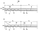
図5(a)は本発明の実施形態に係るタッチパネル用積層体の第3の例を示す模式的断面図であり、(b)はタッチパネル用積層体の第3の例の剥離フィルムを剥した状態を示す模式的断面図である。
図5(a)および(b)において、図2(a)に示すタッチパネル用積層体10と同一構成物には、同一符号を付して、その詳細な説明は省略する。
図5(a)および(b)において、図2(a)に示すタッチパネル用積層体10と同一構成物には、同一符号を付して、その詳細な説明は省略する。
図5(a)に示すタッチパネル用積層体10bは、積層体24の構成が図2(a)に示すタッチパネル用積層体10の積層体12に比して、センサーシート16の表面16aに粘着剤層26が設けられ、粘着剤層26の表面26aに剥離フィルム28が設けられている点が異なり、それ以外の構成は、図2(a)に示すタッチパネル用積層体10の積層体12と同じ構成であるため、その詳細な説明は省略する。
粘着剤層26は、タッチパネル用積層体10bを他の部材と接着するためのものである。粘着剤層26には、例えば、光学的透明な粘着剤(OCA、Optical Clear Adhesive)およびUV(Ultra Violet)硬化樹脂等の光学的透明な樹脂(OCR、Optical Clear Resin)を用いることができる。粘着剤層26については、後に詳細に説明は省略する。
ここで、光学的透明および単に透明とは、いずれも光透過率が、波長400~800nmの可視光波長域において、少なくとも60%以上のことであり、好ましくは75%以上であり、より好ましくは80%以上、さらにより好ましくは85%以上のことである。光透過率は、例えば、JIS K 7375:2008に規定される「プラスチック--全光線透過率及び全光線反射率の求め方」を用いて測定されるものである。
ここで、光学的透明および単に透明とは、いずれも光透過率が、波長400~800nmの可視光波長域において、少なくとも60%以上のことであり、好ましくは75%以上であり、より好ましくは80%以上、さらにより好ましくは85%以上のことである。光透過率は、例えば、JIS K 7375:2008に規定される「プラスチック--全光線透過率及び全光線反射率の求め方」を用いて測定されるものである。
剥離フィルム28は、粘着剤層26を保護するものであり、かつ粘着剤層26を使用する際には取り除くことができるものである。剥離フィルム28は、粘着剤層26の表面26aに、粘着剤層26に対して剥離可能に設けられている。剥離フィルム28は粘着剤層26から剥離した際に、剥離フィルム28の一部でも粘着剤層26に残留しないことが好ましい。剥離フィルム28は、例えば、シリコーン系樹脂またはフッ素系樹脂により構成される。剥離フィルム28については後に説明は省略する。
図5(a)に示すタッチパネル用積層体10bは、剥離フィルム28を剥して、粘着剤層26の表面26aに別の部材が貼り付けられるが、第2の領域S2に凹凸14を設けることによって、図5(b)に示すように剥離フィルム28を方向Pに剥す際に、センサーシート16と保護フィルム18との界面Bでの剥離が抑制される。凹凸14により物理的に、センサーシート16と保護フィルム18との密着力、すなわち、剥離強度を向上させているため、保護フィルム18の粘着剤の密着力を上げる必要がなく、保護フィルム18の粘着剤がセンサーシート16に転写することもない。
図5(a)に示すタッチパネル用積層体10bでは、剥離フィルム28を剥す際に生じる力に応じて、凹凸14を設ける量、配置密度を適宜決定することが好ましい。また、剥離フィルム28を剥す位置に応じて、凹凸14を設ける位置を変えるようにしてもよい。例えば、剥離フィルム28を剥す際に、積層体24で第2の領域S2において力が掛る領域を特定しておき、その第2の領域S2における領域に凹凸14を設けてもよい。
図5(a)に示すタッチパネル用積層体10bでは、剥離フィルム28を剥す際に生じる力に応じて、凹凸14を設ける量、配置密度を適宜決定することが好ましい。また、剥離フィルム28を剥す位置に応じて、凹凸14を設ける位置を変えるようにしてもよい。例えば、剥離フィルム28を剥す際に、積層体24で第2の領域S2において力が掛る領域を特定しておき、その第2の領域S2における領域に凹凸14を設けてもよい。
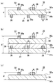
図6(a)は本発明のタッチパネル用積層体のセンサーシートの第1の例を示す模式的断面図であり、(b)は本発明のタッチパネル用積層体のセンサーシートの第2の例を示す模式的断面図であり、(c)は本発明のタッチパネル用積層体のセンサーシートの第3の例を示す模式的断面図である。
センサーシート16は、図6(a)に示すように、基板30の表面30aに第1の検出部32が形成され、基板30の裏面30bに第2の検出部34が形成されている。第1の検出部32および第2の検出部34は導電性細線36により構成される。1つの基板30の表面30aに第1の検出部32を形成し、裏面30bに第2の検出部34を形成することにより、基板30が収縮しても第1の検出部32と第2の検出部34との位置関係のズレを小さくすることができる。
図6(a)に示すセンサーシート16の厚みdは、第1の検出部32の導電性細線36の表面36aと第2の検出部34の導電性細線36の表面36aとの距離である。
センサーシート16は、図6(a)に示すように、基板30の表面30aに第1の検出部32が形成され、基板30の裏面30bに第2の検出部34が形成されている。第1の検出部32および第2の検出部34は導電性細線36により構成される。1つの基板30の表面30aに第1の検出部32を形成し、裏面30bに第2の検出部34を形成することにより、基板30が収縮しても第1の検出部32と第2の検出部34との位置関係のズレを小さくすることができる。
図6(a)に示すセンサーシート16の厚みdは、第1の検出部32の導電性細線36の表面36aと第2の検出部34の導電性細線36の表面36aとの距離である。
図6(b)に示すセンサーシート16のように、1つの基板に1つの検出部を設ける構成でもよい。センサーシート16は、1つの基板30の表面30aに第1の検出部32が形成された、基板30の裏面30bに、接着層38を介して表面31aに第2の検出部34が形成された基板31が積層された構成でもよい。なお、基板31は基板30と同じ構成である。
図6(b)に示すセンサーシート16の厚みdは、第1の検出部32の導電性細線36の表面36aと基板31の裏面31bとの距離である。
図6(b)に示すセンサーシート16の厚みdは、第1の検出部32の導電性細線36の表面36aと基板31の裏面31bとの距離である。
センサーシート16は、2つの検出部を設けたが、これに限定されるものではない。例えば、図6(c)に示すように、1つの基板30の表面30aに第1の検出部32が設けられた構成でもよい。
図6(c)に示すセンサーシート16の厚みdは、第1の検出部32の導電性細線36の表面36aと基板30の裏面30bとの距離である。
センサーシート16の厚みdについては、導電性細線36を含むセンサーシート16の断面画像を取得し、断面画像をパーソナルコンピュータに取り見込み、モニタに表示し、モニタ上で上述のセンサーシート16の厚みdを規定する2箇所に、それぞれ水平線をひき、水平線間の長さを求める。これにより、センサーシート16の厚みdを得ることができる。
導電性細線36の線幅wおよび導電性細線36の厚みtは、上述のセンサーシート16の厚みdと同様に、センサーシート16の断面画像を用いて測定することができる。
図6(c)に示すセンサーシート16の厚みdは、第1の検出部32の導電性細線36の表面36aと基板30の裏面30bとの距離である。
センサーシート16の厚みdについては、導電性細線36を含むセンサーシート16の断面画像を取得し、断面画像をパーソナルコンピュータに取り見込み、モニタに表示し、モニタ上で上述のセンサーシート16の厚みdを規定する2箇所に、それぞれ水平線をひき、水平線間の長さを求める。これにより、センサーシート16の厚みdを得ることができる。
導電性細線36の線幅wおよび導電性細線36の厚みtは、上述のセンサーシート16の厚みdと同様に、センサーシート16の断面画像を用いて測定することができる。
以下、センサーシート、剥離フィルム、保護フィルムの各部材について説明する。
<基板>
基板は、第1の検出部、第1の周辺配線、第2の検出部、第2の周辺配線を支持することができれば、その種類は特に限定されるものではないが、透明基材であることが好ましく、特にプラスチックフィルムが好ましい。
基板を構成する材料の具体例としては、PET(ポリエチレンテレフタレート)(258℃)、ポリシクロオレフィン(134℃)、ポリカーボネート(250℃)、アクリル樹脂(128℃)、PEN(ポリエチレンナフタレート)(269℃)、PE(ポリエチレン)(135℃)、PP(ポリプロピレン)(163℃)、ポリスチレン(230℃)、ポリ塩化ビニル(180℃)、ポリ塩化ビニリデン(212℃)およびTAC(トリアセチルセルロース)(290℃)等の融点が約290℃以下であるプラスチックフィルムが好ましく、特に、PET、ポリシクロオレフィン、ポリカーボネートが好ましい。( )内の数値は融点である。
<基板>
基板は、第1の検出部、第1の周辺配線、第2の検出部、第2の周辺配線を支持することができれば、その種類は特に限定されるものではないが、透明基材であることが好ましく、特にプラスチックフィルムが好ましい。
基板を構成する材料の具体例としては、PET(ポリエチレンテレフタレート)(258℃)、ポリシクロオレフィン(134℃)、ポリカーボネート(250℃)、アクリル樹脂(128℃)、PEN(ポリエチレンナフタレート)(269℃)、PE(ポリエチレン)(135℃)、PP(ポリプロピレン)(163℃)、ポリスチレン(230℃)、ポリ塩化ビニル(180℃)、ポリ塩化ビニリデン(212℃)およびTAC(トリアセチルセルロース)(290℃)等の融点が約290℃以下であるプラスチックフィルムが好ましく、特に、PET、ポリシクロオレフィン、ポリカーボネートが好ましい。( )内の数値は融点である。
基板の全光線透過率は、85%~100%であることが好ましい。全光透過率は、例えば、JIS K 7375:2008に規定される「プラスチック--全光線透過率及び全光線反射率の求め方」を用いて測定されるものである。
基板の厚みは、センサーシートの厚みdが50μm以下になるものが選択される。基板の厚みは、5~40μmが好ましく、最も好ましくは10~30μmである。
基板の厚みは、センサーシートの厚みdが50μm以下になるものが選択される。基板の厚みは、5~40μmが好ましく、最も好ましくは10~30μmである。
基板の好適態様の1つとしては、大気圧プラズマ処理、コロナ放電処理、および紫外線照射処理からなる群から選択される少なくとも1つの処理が施された処理済基板が挙げられる。上述の処理が施されることにより、処理された基板の面にはOH基等の親水性基が導入され、第1の検出部、第1の周辺配線、第2の検出部、および第2の周辺配線の基板との密着性がより向上する。
上述の処理の中でも、第1の検出部、第1の周辺配線、第2の検出部、および第2の周辺配線の基板との密着性がより向上する点で、大気圧プラズマ処理が好ましい。
上述の処理の中でも、第1の検出部、第1の周辺配線、第2の検出部、および第2の周辺配線の基板との密着性がより向上する点で、大気圧プラズマ処理が好ましい。
基板の他の好適態様としては、第1の検出部、第1の周辺配線、第2の検出部、第2の周辺配線が設けられる面上に高分子を含む下塗り層を有することが好ましい。この下塗り層上に、第1の検出部、第1の周辺配線、第2の検出部、および第2の周辺配線を形成するための感光性層が形成されることにより、第1の検出部、第1の周辺配線、第2の検出部、および第2の周辺配線の基板との密着性がより向上する。
下塗り層の形成方法は特に限定されるものではないが、例えば、高分子を含む下塗り層形成用組成物を基板上に塗布して、必要に応じて加熱処理を施す方法が挙げられる。下塗り層形成用組成物には、必要に応じて、溶媒が含まれていてもよい。溶媒の種類は特に限定されるものではないが、後述する感光性層形成用組成物で使用される溶媒が例示される。また、高分子を含む下塗り層形成用組成物として、高分子の微粒子を含むラテックスを使用してもよい。
下塗り層の厚みは特に限定されるものではないが、第1の検出部、第1の周辺配線、第2の検出部、および第2の周辺配線の基板との密着性がより優れる点で、0.02~0.3μmが好ましく、0.03~0.2μmがより好ましい。
下塗り層の形成方法は特に限定されるものではないが、例えば、高分子を含む下塗り層形成用組成物を基板上に塗布して、必要に応じて加熱処理を施す方法が挙げられる。下塗り層形成用組成物には、必要に応じて、溶媒が含まれていてもよい。溶媒の種類は特に限定されるものではないが、後述する感光性層形成用組成物で使用される溶媒が例示される。また、高分子を含む下塗り層形成用組成物として、高分子の微粒子を含むラテックスを使用してもよい。
下塗り層の厚みは特に限定されるものではないが、第1の検出部、第1の周辺配線、第2の検出部、および第2の周辺配線の基板との密着性がより優れる点で、0.02~0.3μmが好ましく、0.03~0.2μmがより好ましい。
<導電性細線>
導電性細線は、電気導電性を有するものであり、例えば、金属、合金、ならびにITO(Indium Tin Oxide)およびZnO等の金属酸化物等により構成される。導電性細線は、例えば、スパッタ法、蒸着法により形成される。これ以外にも、導電性細線は、例えば、蒸着法により金属層を形成し、フォトリソグラフィー法を用いてパターニングして形成することもできる。
導電性細線を金属細線により構成する場合、例えば、銅線または銀線により構成することができる。金属細線には、金属銀が含まれることが好ましいが、金属銀以外の金属、例えば、金、銅等が含まれていてもよい。また、金属細線には金属銀およびゼラチン等の高分子バインダーが含有されたものであることが好ましい。
導電性細線は、電気導電性を有するものであり、例えば、金属、合金、ならびにITO(Indium Tin Oxide)およびZnO等の金属酸化物等により構成される。導電性細線は、例えば、スパッタ法、蒸着法により形成される。これ以外にも、導電性細線は、例えば、蒸着法により金属層を形成し、フォトリソグラフィー法を用いてパターニングして形成することもできる。
導電性細線を金属細線により構成する場合、例えば、銅線または銀線により構成することができる。金属細線には、金属銀が含まれることが好ましいが、金属銀以外の金属、例えば、金、銅等が含まれていてもよい。また、金属細線には金属銀およびゼラチン等の高分子バインダーが含有されたものであることが好ましい。
導電性細線は、上述の金属、合金、金属酸化物単体で構成されるものに限定されるものではなく、例えば、金属酸化物粒子、銀ペーストおよびは銅ペースト等の金属ペースト、ならびに銀ナノワイヤおよび銅ナノワイヤ等の金属ナノワイヤ粒子を含むものであってもよい。
導電性細線によりメッシュパターンを形成することもできる。この場合、導電性細線は、金属細線、合金細線および金属酸化物薄膜であることが好ましく、金属細線からなることが特に好ましく、上述の金属銀およびゼラチン等の高分子バインダーが含有されたものであることが更に好ましい。
導電性細線によりメッシュパターンを形成することもできる。この場合、導電性細線は、金属細線、合金細線および金属酸化物薄膜であることが好ましく、金属細線からなることが特に好ましく、上述の金属銀およびゼラチン等の高分子バインダーが含有されたものであることが更に好ましい。
導電性細線が金属細線の場合、導電性細線の線幅wは、特に限定されるものではないが、30μm以下が好ましく、15μm以下がより好ましく、10μm以下がさらに好ましく、9μm以下が特に好ましく、7μm以下が最も好ましく、0.5μm以上が好ましく、1.0μm以上がより好ましい。線幅wが上述の範囲であれば、低抵抗の検出電極を比較的容易に形成できる。
導電性細線が周辺配線(引き出し配線)として適用される場合には、導電性細線の線幅wは500μm以下が好ましく、50μm以下がより好ましく、30μm以下が特に好ましい。線幅wが上述の範囲であれば、低抵抗の周辺配線を比較的容易に形成できる。
導電性細線が周辺配線(引き出し配線)として適用される場合には、導電性細線の線幅wは500μm以下が好ましく、50μm以下がより好ましく、30μm以下が特に好ましい。線幅wが上述の範囲であれば、低抵抗の周辺配線を比較的容易に形成できる。
また、導電性細線が金属細線の場合、導電性細線が導電フィルムにおける周辺配線として適用される場合、センサーシートにおける周辺配線は、検出電極と同じくメッシュパターンとすることもでき、その場合、線幅wは特に限定されるものではないが、30μm以下が好ましく、15μm以下がより好ましく、10μm以下がさらに好ましく、9μm以下が特に好ましく、7μm以下が最も好ましく、0.5μm以上が好ましく、1.0μm以上がより好ましい。線幅wが上述の範囲であれば、低抵抗の周辺配線を比較的容易に形成できる。センサーシートにおける周辺配線をメッシュパターンとすることによって、検出電極を形成する際に、キセノンフラッシュランプからのパルス光を照射する工程において、検出電極と周辺配線の照射による低抵抗化の均一性を高めることができる他、粘着剤層を貼合した場合に、検出電極と周辺配線のピール強度を一定にでき、面内分布が小さくできる点で好ましい。
導電性細線が金属細線の場合、導電性細線の厚みtは、特に限定されるものではないが、1~200μmが好ましく、30μm以下であることがより好ましく、20μm以下であることがさらに好ましく、0.01~9μmであることが特に好ましく、0.05~5μmであることが最も好ましい。厚みtが上述の範囲であれば、低抵抗で、かつ耐久性に優れた検出電極を比較的容易に形成できる。
<検出電極>
検出電極のパターンは、特に限定されるものではないが、正三角形、二等辺三角形、直角三角形等の三角形、正方形、長方形、菱形、平行四辺形、台形等の四角形、(正)六角形、(正)八角形等の(正)n角形、円、楕円、星形等を組み合わせた幾何学図形であることが好ましく、これらの幾何学図形からなるメッシュパターンであることが更に好ましい。メッシュパターンとは、導電性細線により格子状に構成されたセルが多数組み合わされてなるものである。具体的には、図4(b)に示すように、基板の同じ面上に形成された、交差する導電性細線36により構成される複数の正方形状の格子が多数組み合わされたパターンを意図する。メッシュパターンとしては、相似形、合同な形状の格子が組み合わされた構成でもよく、異なる形状の格子が組み合わされたものでもよい。
検出電極のパターンは、特に限定されるものではないが、正三角形、二等辺三角形、直角三角形等の三角形、正方形、長方形、菱形、平行四辺形、台形等の四角形、(正)六角形、(正)八角形等の(正)n角形、円、楕円、星形等を組み合わせた幾何学図形であることが好ましく、これらの幾何学図形からなるメッシュパターンであることが更に好ましい。メッシュパターンとは、導電性細線により格子状に構成されたセルが多数組み合わされてなるものである。具体的には、図4(b)に示すように、基板の同じ面上に形成された、交差する導電性細線36により構成される複数の正方形状の格子が多数組み合わされたパターンを意図する。メッシュパターンとしては、相似形、合同な形状の格子が組み合わされた構成でもよく、異なる形状の格子が組み合わされたものでもよい。
なお、必要に応じて、導電フィルムは、基材と導電部との間に他の層として、上述の下塗り層以外に、例えば、アンチハレーション層を備えていてもよい。
上述のセンサーシートの製造方法は特に限定されるものではないが、公知の方法を適用することができる。
上述のセンサーシートの製造方法は特に限定されるものではないが、公知の方法を適用することができる。
<絶縁膜>
センサーシートが周辺配線を有する場合、センサーシートは、上述の周辺配線の少なくとも一部を覆う絶縁膜を有することが好ましい。すなわち、第2の領域S2の一部を覆う絶縁膜を有することが好ましい。
絶縁膜は、特に限定されるものではないが、UV(Ultra Violet)硬化性絶縁樹脂を塗布してUV光によって硬化したもの、熱硬化性絶縁樹脂を塗布して熱によって硬化したものが好ましく、特に、UV硬化性絶縁樹脂を塗布してUV光によって硬化したものが好ましい。
絶縁膜の幅および厚みについては、センサーシートの第2の領域S2の大きさ、周辺配線の厚み等に応じて適宜決定されるものである。絶縁膜がある場合、センサーシートの厚みdは絶縁膜を含め最も厚い部分の厚みとなる。
センサーシートが周辺配線を有する場合、センサーシートは、上述の周辺配線の少なくとも一部を覆う絶縁膜を有することが好ましい。すなわち、第2の領域S2の一部を覆う絶縁膜を有することが好ましい。
絶縁膜は、特に限定されるものではないが、UV(Ultra Violet)硬化性絶縁樹脂を塗布してUV光によって硬化したもの、熱硬化性絶縁樹脂を塗布して熱によって硬化したものが好ましく、特に、UV硬化性絶縁樹脂を塗布してUV光によって硬化したものが好ましい。
絶縁膜の幅および厚みについては、センサーシートの第2の領域S2の大きさ、周辺配線の厚み等に応じて適宜決定されるものである。絶縁膜がある場合、センサーシートの厚みdは絶縁膜を含め最も厚い部分の厚みとなる。
<剥離フィルム>
剥離フィルムとしては、例えば、表面をシリコーン系剥離剤またはその他の剥離剤で処理したフィルム、それ自体が剥離性を有するフィルム、支持体上に密着層が形成されたフィルム等を用いることができる。フィルムおよび支持体を構成する材料は特に限定されるものではないが、例えば、上述の基板で例示された材料が挙げられ、好適な態様も同様である。なかでも、PETが好ましい。また、密着層を形成する材料の具体例は、後述の粘着剤層に記載の粘着剤と同じである。
剥離フィルムの厚みは特に限定されるものではないが、50~200μmが好ましく、75~125μmがより好ましい。剥離フィルム28は、例えば、上述した表面をシリコーン系剥離剤またはその他の剥離剤で処理したフィルムである。
支持体としては、例えば、ポリエチレンテレフタレート(PET)、ポリエチレンナフタレート(PEN)等のポリエステル、ポリカーボネート(PC)、ポリメチルメタクリレート(PMMA)、シクロオレフィンポリマー(COP)、トリアセチルセルロース(TAC)、ポリアリレート(PAR)、ポリスルフォン(PSU)、ポリスチレン(PS)等を用いることができる。
剥離フィルムとしては、例えば、表面をシリコーン系剥離剤またはその他の剥離剤で処理したフィルム、それ自体が剥離性を有するフィルム、支持体上に密着層が形成されたフィルム等を用いることができる。フィルムおよび支持体を構成する材料は特に限定されるものではないが、例えば、上述の基板で例示された材料が挙げられ、好適な態様も同様である。なかでも、PETが好ましい。また、密着層を形成する材料の具体例は、後述の粘着剤層に記載の粘着剤と同じである。
剥離フィルムの厚みは特に限定されるものではないが、50~200μmが好ましく、75~125μmがより好ましい。剥離フィルム28は、例えば、上述した表面をシリコーン系剥離剤またはその他の剥離剤で処理したフィルムである。
支持体としては、例えば、ポリエチレンテレフタレート(PET)、ポリエチレンナフタレート(PEN)等のポリエステル、ポリカーボネート(PC)、ポリメチルメタクリレート(PMMA)、シクロオレフィンポリマー(COP)、トリアセチルセルロース(TAC)、ポリアリレート(PAR)、ポリスルフォン(PSU)、ポリスチレン(PS)等を用いることができる。
<粘着層>
剥離フィルムの粘着層としては、特に限定されるものではないが、ゴム系粘着剤、アクリル系粘着剤、およびシリコーン系粘着剤等が挙げられる。なかでも、透明性に優れる観点から、アクリル系粘着剤が好ましい。
アクリル系粘着剤は、アルキル(メタ)アクリレート由来の繰り返し単位を有するアクリル系ポリマーを主成分としたものであるのが好ましい。なお、(メタ)アクリレートは、アクリレートおよび/またはメタクリレートをいう。アクリル系ポリマーは、アルキル基の炭素数が1~12程度であるアルキル(メタ)アクリレート由来の繰り返し単位を有するアクリル系ポリマーであることが好ましく、上述の炭素数のアルキルメタクリレート由来の繰り返し単位および上述の炭素数のアルキルアクリレート由来の繰り返し単位を有するアクリル系ポリマーがより好ましい。上述のアクリル系ポリマー中の繰り返し単位のなかには、(メタ)アクリル酸由来の繰り返し単位が含まれていてもよい。
粘着剤層の厚みは特に限定されるものではないが、25~300μmであることが好ましく、50~200μmであることがより好ましい。
剥離フィルムの粘着層としては、特に限定されるものではないが、ゴム系粘着剤、アクリル系粘着剤、およびシリコーン系粘着剤等が挙げられる。なかでも、透明性に優れる観点から、アクリル系粘着剤が好ましい。
アクリル系粘着剤は、アルキル(メタ)アクリレート由来の繰り返し単位を有するアクリル系ポリマーを主成分としたものであるのが好ましい。なお、(メタ)アクリレートは、アクリレートおよび/またはメタクリレートをいう。アクリル系ポリマーは、アルキル基の炭素数が1~12程度であるアルキル(メタ)アクリレート由来の繰り返し単位を有するアクリル系ポリマーであることが好ましく、上述の炭素数のアルキルメタクリレート由来の繰り返し単位および上述の炭素数のアルキルアクリレート由来の繰り返し単位を有するアクリル系ポリマーがより好ましい。上述のアクリル系ポリマー中の繰り返し単位のなかには、(メタ)アクリル酸由来の繰り返し単位が含まれていてもよい。
粘着剤層の厚みは特に限定されるものではないが、25~300μmであることが好ましく、50~200μmであることがより好ましい。
<保護フィルム>
保護フィルムの基材には、剥離フィルムの支持体と同様のものを用いることができる。また、保護フィルムの粘着層には、上述の剥離フィルムの粘着層と同様のものを用いることができる。
保護フィルムの基材には、剥離フィルムの支持体と同様のものを用いることができる。また、保護フィルムの粘着層には、上述の剥離フィルムの粘着層と同様のものを用いることができる。
本発明は、基本的に以上のように構成されるものである。以上、本発明のタッチパネル用積層体について詳細に説明したが、本発明は上述の実施形態に限定されず、本発明の主旨を逸脱しない範囲において、種々の改良または変更をしてもよいのはもちろんである。
10、10a、10b タッチパネル用積層体
12、20、24 積層体
14 凹凸
16 センサーシート
18 保護フィルム
22 第1の保護フィルム
23 第2の保護フィルム
26 粘着剤層
28 剥離フィルム
30 基板
32 第1の検出部
33 第1の周辺配線
34 第2の検出部
35 第2の周辺配線
36 導電性細線
38 接着層
40 基材
42 粘着層
B 界面
S1 第1の領域
S2 第2の領域
12、20、24 積層体
14 凹凸
16 センサーシート
18 保護フィルム
22 第1の保護フィルム
23 第2の保護フィルム
26 粘着剤層
28 剥離フィルム
30 基板
32 第1の検出部
33 第1の周辺配線
34 第2の検出部
35 第2の周辺配線
36 導電性細線
38 接着層
40 基材
42 粘着層
B 界面
S1 第1の領域
S2 第2の領域
Claims (7)
- 基板および検出電極を備えるセンサーシートと、前記センサーシートの少なくとも一方の面に積層された、前記センサーシートを保護する保護フィルムとを有する積層体を備えるタッチパネル用積層体であって、
前記センサーシートは厚みが50μm以下であり、
前記積層体において、前記検出電極が設けられた領域を第1の領域とし、前記第1の領域以外の領域を第2の領域とするとき、前記積層体には前記第2の領域に凹凸が設けられていることを特徴とするタッチパネル用積層体。 - 前記積層体は、平面視、複数の角部を有する矩形状であり、前記第2の領域は前記積層体の前記角部を含む周辺部にあり、前記凹凸は、前記積層体の少なくとも1つの角部に設けられている請求項1に記載のタッチパネル用積層体。
- 前記凹凸は、点状に不連続に、または線状に連続に設けられている請求項1に記載のタッチパネル用積層体。
- 前記保護フィルムが前記センサーシートの一方の面に設けられており、
前記センサーシートの他方の面上に粘着剤層が設けられ、前記粘着剤層上に、前記粘着剤層に対して剥離可能な剥離フィルムが設けられている請求項1~3のいずれか1項に記載のタッチパネル用積層体。 - 前記保護フィルムは、前記センサーシートの両面に設けられており、前記凹凸は、一方の保護フィルムと前記センサーシートに設けられている請求項1または2に記載のタッチパネル用積層体。
- 前記検出電極は、メッシュパターンを有する請求項1~5のいずれか1項に記載のタッチパネル用積層体。
- 前記保護フィルムは、基材上に粘着層が設けられたものであり、前記保護フィルムは、前記粘着層を前記センサーシートに向けて、前記センサーシートと積層されている請求項1~6のいずれか1項に記載のタッチパネル用積層体。
Applications Claiming Priority (2)
| Application Number | Priority Date | Filing Date | Title |
|---|---|---|---|
| JP2015-228503 | 2015-11-24 | ||
| JP2015228503A JP2019015996A (ja) | 2015-11-24 | 2015-11-24 | タッチパネル用積層体 |
Publications (1)
| Publication Number | Publication Date |
|---|---|
| WO2017090323A1 true WO2017090323A1 (ja) | 2017-06-01 |
Family
ID=58763815
Family Applications (1)
| Application Number | Title | Priority Date | Filing Date |
|---|---|---|---|
| PCT/JP2016/079564 Ceased WO2017090323A1 (ja) | 2015-11-24 | 2016-10-05 | タッチパネル用積層体 |
Country Status (2)
| Country | Link |
|---|---|
| JP (1) | JP2019015996A (ja) |
| WO (1) | WO2017090323A1 (ja) |
Citations (3)
| Publication number | Priority date | Publication date | Assignee | Title |
|---|---|---|---|---|
| JP2012113641A (ja) * | 2010-11-26 | 2012-06-14 | Alps Electric Co Ltd | 入力装置及び入力装置の製造方法 |
| JP2013190715A (ja) * | 2012-03-15 | 2013-09-26 | Japan Display West Co Ltd | 表示装置、製造方法、電子機器 |
| JP2015176573A (ja) * | 2014-03-18 | 2015-10-05 | 株式会社ジャパンディスプレイ | 電極基板、表示装置、入力装置および電極基板の製造方法 |
-
2015
- 2015-11-24 JP JP2015228503A patent/JP2019015996A/ja active Pending
-
2016
- 2016-10-05 WO PCT/JP2016/079564 patent/WO2017090323A1/ja not_active Ceased
Patent Citations (3)
| Publication number | Priority date | Publication date | Assignee | Title |
|---|---|---|---|---|
| JP2012113641A (ja) * | 2010-11-26 | 2012-06-14 | Alps Electric Co Ltd | 入力装置及び入力装置の製造方法 |
| JP2013190715A (ja) * | 2012-03-15 | 2013-09-26 | Japan Display West Co Ltd | 表示装置、製造方法、電子機器 |
| JP2015176573A (ja) * | 2014-03-18 | 2015-10-05 | 株式会社ジャパンディスプレイ | 電極基板、表示装置、入力装置および電極基板の製造方法 |
Also Published As
| Publication number | Publication date |
|---|---|
| JP2019015996A (ja) | 2019-01-31 |
Similar Documents
| Publication | Publication Date | Title |
|---|---|---|
| CN107111392B (zh) | 导电性薄膜及具备该导电性薄膜的触摸面板传感器 | |
| TWI584163B (zh) | Touch panel sensors, touch panel devices and display devices | |
| TWI746795B (zh) | 觸控面板及觸控面板用導電性片及觸控感測器 | |
| JP6449615B2 (ja) | タッチウィンドウ及びこれを含むタッチデバイス | |
| CN102365612B (zh) | 电功能层及其制造方法和使用 | |
| TWI509477B (zh) | 觸控面板及其製造方法 | |
| TWI628565B (zh) | 導電片、靜電容式觸控面板以及顯示裝置 | |
| US11494013B2 (en) | Touch panel and fabricating method thereof | |
| JP2013122745A (ja) | タッチパネル及びその製造方法 | |
| US10261639B2 (en) | Touch display device and method of manufacturing the same | |
| KR20120137216A (ko) | 터치 스크린 센서 기판, 터치 스크린 센서 및 이를 포함하는 패널 | |
| JP6799664B2 (ja) | タッチセンサ、タッチパネル、タッチパネル用導電部材およびタッチパネル用導電性シート | |
| CN106415462B (zh) | 触摸窗 | |
| CN103135869B (zh) | 触摸面板传感器 | |
| TW201245811A (en) | Input device and method of manufacturing the same | |
| CN103744571A (zh) | 超薄触控传感器及其制作方法 | |
| KR101337913B1 (ko) | 터치 스크린 센서 및 이를 포함하는 터치 스크린 패널 | |
| JP2016506574A (ja) | 反射防止層を含むタッチパネルおよびその製造方法 | |
| CN203085197U (zh) | 透明导电性薄膜 | |
| JPWO2019021835A1 (ja) | タッチパネル用導電部材およびタッチパネル | |
| TW201611043A (zh) | 導電膜 | |
| TWM488681U (zh) | 觸控面板 | |
| CN203909742U (zh) | 触控显示面板 | |
| WO2017090323A1 (ja) | タッチパネル用積層体 | |
| TWI588700B (zh) | 觸控裝置 |
Legal Events
| Date | Code | Title | Description |
|---|---|---|---|
| 121 | Ep: the epo has been informed by wipo that ep was designated in this application |
Ref document number: 16868272 Country of ref document: EP Kind code of ref document: A1 |
|
| NENP | Non-entry into the national phase |
Ref country code: DE |
|
| 122 | Ep: pct application non-entry in european phase |
Ref document number: 16868272 Country of ref document: EP Kind code of ref document: A1 |
|
| NENP | Non-entry into the national phase |
Ref country code: JP |