WO2017082270A1 - 導電性フィルム - Google Patents
導電性フィルム Download PDFInfo
- Publication number
- WO2017082270A1 WO2017082270A1 PCT/JP2016/083170 JP2016083170W WO2017082270A1 WO 2017082270 A1 WO2017082270 A1 WO 2017082270A1 JP 2016083170 W JP2016083170 W JP 2016083170W WO 2017082270 A1 WO2017082270 A1 WO 2017082270A1
- Authority
- WO
- WIPO (PCT)
- Prior art keywords
- conductive
- film
- layer
- material layer
- conductive material
- Prior art date
- Legal status (The legal status is an assumption and is not a legal conclusion. Google has not performed a legal analysis and makes no representation as to the accuracy of the status listed.)
- Ceased
Links
Images









Classifications
-
- B—PERFORMING OPERATIONS; TRANSPORTING
- B32—LAYERED PRODUCTS
- B32B—LAYERED PRODUCTS, i.e. PRODUCTS BUILT-UP OF STRATA OF FLAT OR NON-FLAT, e.g. CELLULAR OR HONEYCOMB, FORM
- B32B25/00—Layered products comprising a layer of natural or synthetic rubber
- B32B25/04—Layered products comprising a layer of natural or synthetic rubber comprising rubber as the main or only constituent of a layer, which is next to another layer of the same or of a different material
- B32B25/042—Layered products comprising a layer of natural or synthetic rubber comprising rubber as the main or only constituent of a layer, which is next to another layer of the same or of a different material of natural rubber or synthetic rubber
-
- B—PERFORMING OPERATIONS; TRANSPORTING
- B32—LAYERED PRODUCTS
- B32B—LAYERED PRODUCTS, i.e. PRODUCTS BUILT-UP OF STRATA OF FLAT OR NON-FLAT, e.g. CELLULAR OR HONEYCOMB, FORM
- B32B25/00—Layered products comprising a layer of natural or synthetic rubber
- B32B25/04—Layered products comprising a layer of natural or synthetic rubber comprising rubber as the main or only constituent of a layer, which is next to another layer of the same or of a different material
- B32B25/045—Layered products comprising a layer of natural or synthetic rubber comprising rubber as the main or only constituent of a layer, which is next to another layer of the same or of a different material of foam
-
- B—PERFORMING OPERATIONS; TRANSPORTING
- B32—LAYERED PRODUCTS
- B32B—LAYERED PRODUCTS, i.e. PRODUCTS BUILT-UP OF STRATA OF FLAT OR NON-FLAT, e.g. CELLULAR OR HONEYCOMB, FORM
- B32B25/00—Layered products comprising a layer of natural or synthetic rubber
- B32B25/04—Layered products comprising a layer of natural or synthetic rubber comprising rubber as the main or only constituent of a layer, which is next to another layer of the same or of a different material
- B32B25/08—Layered products comprising a layer of natural or synthetic rubber comprising rubber as the main or only constituent of a layer, which is next to another layer of the same or of a different material of synthetic resin
-
- B—PERFORMING OPERATIONS; TRANSPORTING
- B32—LAYERED PRODUCTS
- B32B—LAYERED PRODUCTS, i.e. PRODUCTS BUILT-UP OF STRATA OF FLAT OR NON-FLAT, e.g. CELLULAR OR HONEYCOMB, FORM
- B32B25/00—Layered products comprising a layer of natural or synthetic rubber
- B32B25/14—Layered products comprising a layer of natural or synthetic rubber comprising synthetic rubber copolymers
-
- B—PERFORMING OPERATIONS; TRANSPORTING
- B32—LAYERED PRODUCTS
- B32B—LAYERED PRODUCTS, i.e. PRODUCTS BUILT-UP OF STRATA OF FLAT OR NON-FLAT, e.g. CELLULAR OR HONEYCOMB, FORM
- B32B25/00—Layered products comprising a layer of natural or synthetic rubber
- B32B25/16—Layered products comprising a layer of natural or synthetic rubber comprising polydienes homopolymers or poly-halodienes homopolymers
-
- B—PERFORMING OPERATIONS; TRANSPORTING
- B32—LAYERED PRODUCTS
- B32B—LAYERED PRODUCTS, i.e. PRODUCTS BUILT-UP OF STRATA OF FLAT OR NON-FLAT, e.g. CELLULAR OR HONEYCOMB, FORM
- B32B27/00—Layered products comprising a layer of synthetic resin
- B32B27/06—Layered products comprising a layer of synthetic resin as the main or only constituent of a layer, which is next to another layer of the same or of a different material
- B32B27/065—Layered products comprising a layer of synthetic resin as the main or only constituent of a layer, which is next to another layer of the same or of a different material of foam
-
- B—PERFORMING OPERATIONS; TRANSPORTING
- B32—LAYERED PRODUCTS
- B32B—LAYERED PRODUCTS, i.e. PRODUCTS BUILT-UP OF STRATA OF FLAT OR NON-FLAT, e.g. CELLULAR OR HONEYCOMB, FORM
- B32B27/00—Layered products comprising a layer of synthetic resin
- B32B27/28—Layered products comprising a layer of synthetic resin comprising synthetic resins not wholly covered by any one of the sub-groups B32B27/30 - B32B27/42
- B32B27/283—Layered products comprising a layer of synthetic resin comprising synthetic resins not wholly covered by any one of the sub-groups B32B27/30 - B32B27/42 comprising polysiloxanes
-
- B—PERFORMING OPERATIONS; TRANSPORTING
- B32—LAYERED PRODUCTS
- B32B—LAYERED PRODUCTS, i.e. PRODUCTS BUILT-UP OF STRATA OF FLAT OR NON-FLAT, e.g. CELLULAR OR HONEYCOMB, FORM
- B32B27/00—Layered products comprising a layer of synthetic resin
- B32B27/30—Layered products comprising a layer of synthetic resin comprising vinyl (co)polymers; comprising acrylic (co)polymers
- B32B27/302—Layered products comprising a layer of synthetic resin comprising vinyl (co)polymers; comprising acrylic (co)polymers comprising aromatic vinyl (co)polymers, e.g. styrenic (co)polymers
-
- B—PERFORMING OPERATIONS; TRANSPORTING
- B32—LAYERED PRODUCTS
- B32B—LAYERED PRODUCTS, i.e. PRODUCTS BUILT-UP OF STRATA OF FLAT OR NON-FLAT, e.g. CELLULAR OR HONEYCOMB, FORM
- B32B27/00—Layered products comprising a layer of synthetic resin
- B32B27/32—Layered products comprising a layer of synthetic resin comprising polyolefins
-
- B—PERFORMING OPERATIONS; TRANSPORTING
- B32—LAYERED PRODUCTS
- B32B—LAYERED PRODUCTS, i.e. PRODUCTS BUILT-UP OF STRATA OF FLAT OR NON-FLAT, e.g. CELLULAR OR HONEYCOMB, FORM
- B32B27/00—Layered products comprising a layer of synthetic resin
- B32B27/36—Layered products comprising a layer of synthetic resin comprising polyesters
-
- B—PERFORMING OPERATIONS; TRANSPORTING
- B32—LAYERED PRODUCTS
- B32B—LAYERED PRODUCTS, i.e. PRODUCTS BUILT-UP OF STRATA OF FLAT OR NON-FLAT, e.g. CELLULAR OR HONEYCOMB, FORM
- B32B27/00—Layered products comprising a layer of synthetic resin
- B32B27/36—Layered products comprising a layer of synthetic resin comprising polyesters
- B32B27/365—Layered products comprising a layer of synthetic resin comprising polyesters comprising polycarbonates
-
- B—PERFORMING OPERATIONS; TRANSPORTING
- B32—LAYERED PRODUCTS
- B32B—LAYERED PRODUCTS, i.e. PRODUCTS BUILT-UP OF STRATA OF FLAT OR NON-FLAT, e.g. CELLULAR OR HONEYCOMB, FORM
- B32B27/00—Layered products comprising a layer of synthetic resin
- B32B27/40—Layered products comprising a layer of synthetic resin comprising polyurethanes
-
- B—PERFORMING OPERATIONS; TRANSPORTING
- B32—LAYERED PRODUCTS
- B32B—LAYERED PRODUCTS, i.e. PRODUCTS BUILT-UP OF STRATA OF FLAT OR NON-FLAT, e.g. CELLULAR OR HONEYCOMB, FORM
- B32B3/00—Layered products comprising a layer with external or internal discontinuities or unevennesses, or a layer of non-planar shape; Layered products comprising a layer having particular features of form
- B32B3/10—Layered products comprising a layer with external or internal discontinuities or unevennesses, or a layer of non-planar shape; Layered products comprising a layer having particular features of form characterised by a discontinuous layer, i.e. formed of separate pieces of material
- B32B3/12—Layered products comprising a layer with external or internal discontinuities or unevennesses, or a layer of non-planar shape; Layered products comprising a layer having particular features of form characterised by a discontinuous layer, i.e. formed of separate pieces of material characterised by a layer of regularly- arranged cells, e.g. a honeycomb structure
-
- B—PERFORMING OPERATIONS; TRANSPORTING
- B32—LAYERED PRODUCTS
- B32B—LAYERED PRODUCTS, i.e. PRODUCTS BUILT-UP OF STRATA OF FLAT OR NON-FLAT, e.g. CELLULAR OR HONEYCOMB, FORM
- B32B3/00—Layered products comprising a layer with external or internal discontinuities or unevennesses, or a layer of non-planar shape; Layered products comprising a layer having particular features of form
- B32B3/26—Layered products comprising a layer with external or internal discontinuities or unevennesses, or a layer of non-planar shape; Layered products comprising a layer having particular features of form characterised by a particular shape of the outline of the cross-section of a continuous layer; characterised by a layer with cavities or internal voids ; characterised by an apertured layer
- B32B3/266—Layered products comprising a layer with external or internal discontinuities or unevennesses, or a layer of non-planar shape; Layered products comprising a layer having particular features of form characterised by a particular shape of the outline of the cross-section of a continuous layer; characterised by a layer with cavities or internal voids ; characterised by an apertured layer characterised by an apertured layer, the apertures going through the whole thickness of the layer, e.g. expanded metal, perforated layer, slit layer regular cells B32B3/12
-
- C—CHEMISTRY; METALLURGY
- C08—ORGANIC MACROMOLECULAR COMPOUNDS; THEIR PREPARATION OR CHEMICAL WORKING-UP; COMPOSITIONS BASED THEREON
- C08J—WORKING-UP; GENERAL PROCESSES OF COMPOUNDING; AFTER-TREATMENT NOT COVERED BY SUBCLASSES C08B, C08C, C08F, C08G or C08H
- C08J9/00—Working-up of macromolecular substances to porous or cellular articles or materials; After-treatment thereof
- C08J9/26—Working-up of macromolecular substances to porous or cellular articles or materials; After-treatment thereof by elimination of a solid phase from a macromolecular composition or article, e.g. leaching out
-
- C—CHEMISTRY; METALLURGY
- C08—ORGANIC MACROMOLECULAR COMPOUNDS; THEIR PREPARATION OR CHEMICAL WORKING-UP; COMPOSITIONS BASED THEREON
- C08J—WORKING-UP; GENERAL PROCESSES OF COMPOUNDING; AFTER-TREATMENT NOT COVERED BY SUBCLASSES C08B, C08C, C08F, C08G or C08H
- C08J9/00—Working-up of macromolecular substances to porous or cellular articles or materials; After-treatment thereof
- C08J9/28—Working-up of macromolecular substances to porous or cellular articles or materials; After-treatment thereof by elimination of a liquid phase from a macromolecular composition or article, e.g. drying of coagulum
-
- C—CHEMISTRY; METALLURGY
- C08—ORGANIC MACROMOLECULAR COMPOUNDS; THEIR PREPARATION OR CHEMICAL WORKING-UP; COMPOSITIONS BASED THEREON
- C08J—WORKING-UP; GENERAL PROCESSES OF COMPOUNDING; AFTER-TREATMENT NOT COVERED BY SUBCLASSES C08B, C08C, C08F, C08G or C08H
- C08J9/00—Working-up of macromolecular substances to porous or cellular articles or materials; After-treatment thereof
- C08J9/36—After-treatment
-
- C—CHEMISTRY; METALLURGY
- C08—ORGANIC MACROMOLECULAR COMPOUNDS; THEIR PREPARATION OR CHEMICAL WORKING-UP; COMPOSITIONS BASED THEREON
- C08J—WORKING-UP; GENERAL PROCESSES OF COMPOUNDING; AFTER-TREATMENT NOT COVERED BY SUBCLASSES C08B, C08C, C08F, C08G or C08H
- C08J9/00—Working-up of macromolecular substances to porous or cellular articles or materials; After-treatment thereof
- C08J9/36—After-treatment
- C08J9/365—Coating
-
- H—ELECTRICITY
- H01—ELECTRIC ELEMENTS
- H01B—CABLES; CONDUCTORS; INSULATORS; SELECTION OF MATERIALS FOR THEIR CONDUCTIVE, INSULATING OR DIELECTRIC PROPERTIES
- H01B5/00—Non-insulated conductors or conductive bodies characterised by their form
- H01B5/14—Non-insulated conductors or conductive bodies characterised by their form comprising conductive layers or films on insulating-supports
-
- H—ELECTRICITY
- H05—ELECTRIC TECHNIQUES NOT OTHERWISE PROVIDED FOR
- H05K—PRINTED CIRCUITS; CASINGS OR CONSTRUCTIONAL DETAILS OF ELECTRIC APPARATUS; MANUFACTURE OF ASSEMBLAGES OF ELECTRICAL COMPONENTS
- H05K9/00—Screening of apparatus or components against electric or magnetic fields
-
- B—PERFORMING OPERATIONS; TRANSPORTING
- B32—LAYERED PRODUCTS
- B32B—LAYERED PRODUCTS, i.e. PRODUCTS BUILT-UP OF STRATA OF FLAT OR NON-FLAT, e.g. CELLULAR OR HONEYCOMB, FORM
- B32B2255/00—Coating on the layer surface
- B32B2255/10—Coating on the layer surface on synthetic resin layer or on natural or synthetic rubber layer
-
- B—PERFORMING OPERATIONS; TRANSPORTING
- B32—LAYERED PRODUCTS
- B32B—LAYERED PRODUCTS, i.e. PRODUCTS BUILT-UP OF STRATA OF FLAT OR NON-FLAT, e.g. CELLULAR OR HONEYCOMB, FORM
- B32B2255/00—Coating on the layer surface
- B32B2255/20—Inorganic coating
- B32B2255/205—Metallic coating
-
- B—PERFORMING OPERATIONS; TRANSPORTING
- B32—LAYERED PRODUCTS
- B32B—LAYERED PRODUCTS, i.e. PRODUCTS BUILT-UP OF STRATA OF FLAT OR NON-FLAT, e.g. CELLULAR OR HONEYCOMB, FORM
- B32B2266/00—Composition of foam
- B32B2266/12—Gel
- B32B2266/122—Hydrogel, i.e. a gel containing an aqueous composition
-
- B—PERFORMING OPERATIONS; TRANSPORTING
- B32—LAYERED PRODUCTS
- B32B—LAYERED PRODUCTS, i.e. PRODUCTS BUILT-UP OF STRATA OF FLAT OR NON-FLAT, e.g. CELLULAR OR HONEYCOMB, FORM
- B32B2307/00—Properties of the layers or laminate
- B32B2307/20—Properties of the layers or laminate having particular electrical or magnetic properties, e.g. piezoelectric
-
- B—PERFORMING OPERATIONS; TRANSPORTING
- B32—LAYERED PRODUCTS
- B32B—LAYERED PRODUCTS, i.e. PRODUCTS BUILT-UP OF STRATA OF FLAT OR NON-FLAT, e.g. CELLULAR OR HONEYCOMB, FORM
- B32B2307/00—Properties of the layers or laminate
- B32B2307/40—Properties of the layers or laminate having particular optical properties
- B32B2307/412—Transparent
-
- B—PERFORMING OPERATIONS; TRANSPORTING
- B32—LAYERED PRODUCTS
- B32B—LAYERED PRODUCTS, i.e. PRODUCTS BUILT-UP OF STRATA OF FLAT OR NON-FLAT, e.g. CELLULAR OR HONEYCOMB, FORM
- B32B2307/00—Properties of the layers or laminate
- B32B2307/70—Other properties
- B32B2307/732—Dimensional properties
-
- C—CHEMISTRY; METALLURGY
- C08—ORGANIC MACROMOLECULAR COMPOUNDS; THEIR PREPARATION OR CHEMICAL WORKING-UP; COMPOSITIONS BASED THEREON
- C08J—WORKING-UP; GENERAL PROCESSES OF COMPOUNDING; AFTER-TREATMENT NOT COVERED BY SUBCLASSES C08B, C08C, C08F, C08G or C08H
- C08J2201/00—Foams characterised by the foaming process
- C08J2201/04—Foams characterised by the foaming process characterised by the elimination of a liquid or solid component, e.g. precipitation, leaching out, evaporation
- C08J2201/05—Elimination by evaporation or heat degradation of a liquid phase
- C08J2201/0502—Elimination by evaporation or heat degradation of a liquid phase the liquid phase being organic
-
- C—CHEMISTRY; METALLURGY
- C08—ORGANIC MACROMOLECULAR COMPOUNDS; THEIR PREPARATION OR CHEMICAL WORKING-UP; COMPOSITIONS BASED THEREON
- C08J—WORKING-UP; GENERAL PROCESSES OF COMPOUNDING; AFTER-TREATMENT NOT COVERED BY SUBCLASSES C08B, C08C, C08F, C08G or C08H
- C08J2309/00—Characterised by the use of homopolymers or copolymers of conjugated diene hydrocarbons
-
- C—CHEMISTRY; METALLURGY
- C08—ORGANIC MACROMOLECULAR COMPOUNDS; THEIR PREPARATION OR CHEMICAL WORKING-UP; COMPOSITIONS BASED THEREON
- C08J—WORKING-UP; GENERAL PROCESSES OF COMPOUNDING; AFTER-TREATMENT NOT COVERED BY SUBCLASSES C08B, C08C, C08F, C08G or C08H
- C08J2383/00—Characterised by the use of macromolecular compounds obtained by reactions forming in the main chain of the macromolecule a linkage containing silicon with or without sulfur, nitrogen, oxygen, or carbon only; Derivatives of such polymers
- C08J2383/04—Polysiloxanes
-
- C—CHEMISTRY; METALLURGY
- C08—ORGANIC MACROMOLECULAR COMPOUNDS; THEIR PREPARATION OR CHEMICAL WORKING-UP; COMPOSITIONS BASED THEREON
- C08J—WORKING-UP; GENERAL PROCESSES OF COMPOUNDING; AFTER-TREATMENT NOT COVERED BY SUBCLASSES C08B, C08C, C08F, C08G or C08H
- C08J2400/00—Characterised by the use of unspecified polymers
- C08J2400/26—Elastomers
-
- C—CHEMISTRY; METALLURGY
- C08—ORGANIC MACROMOLECULAR COMPOUNDS; THEIR PREPARATION OR CHEMICAL WORKING-UP; COMPOSITIONS BASED THEREON
- C08J—WORKING-UP; GENERAL PROCESSES OF COMPOUNDING; AFTER-TREATMENT NOT COVERED BY SUBCLASSES C08B, C08C, C08F, C08G or C08H
- C08J2433/00—Characterised by the use of homopolymers or copolymers of compounds having one or more unsaturated aliphatic radicals, each having only one carbon-to-carbon double bond, and only one being terminated by only one carboxyl radical, or of salts, anhydrides, esters, amides, imides, or nitriles thereof; Derivatives of such polymers
- C08J2433/24—Homopolymers or copolymers of amides or imides
- C08J2433/26—Homopolymers or copolymers of acrylamide or methacrylamide
-
- Y—GENERAL TAGGING OF NEW TECHNOLOGICAL DEVELOPMENTS; GENERAL TAGGING OF CROSS-SECTIONAL TECHNOLOGIES SPANNING OVER SEVERAL SECTIONS OF THE IPC; TECHNICAL SUBJECTS COVERED BY FORMER USPC CROSS-REFERENCE ART COLLECTIONS [XRACs] AND DIGESTS
- Y10—TECHNICAL SUBJECTS COVERED BY FORMER USPC
- Y10T—TECHNICAL SUBJECTS COVERED BY FORMER US CLASSIFICATION
- Y10T428/00—Stock material or miscellaneous articles
- Y10T428/24—Structurally defined web or sheet [e.g., overall dimension, etc.]
- Y10T428/24942—Structurally defined web or sheet [e.g., overall dimension, etc.] including components having same physical characteristic in differing degree
- Y10T428/2495—Thickness [relative or absolute]
- Y10T428/24967—Absolute thicknesses specified
Definitions
- the present invention relates to a conductive film.
- biosensors that are non-invasive or minimally invasive to the surface of biological tissues.
- a so-called smart contact lens that detects blood glucose level or intraocular pressure has been proposed.
- a biosensor in the form of a lens such as a smart contact lens, it is desirable that the conductive material used as the electrode material transmits visible light.
- JP-A-11-121974 discloses visible light as an electromagnetic wave shielding plate comprising a transparent resin (polymer) base material and a conductive mesh made of a metal thin film laminated on the resin base material.
- a transparent conductive material is described.
- Japanese Patent Laid-Open No. 2014-175609 discloses a conductive material that transmits visible light, which includes a transparent resin base material and a conductive mesh that is provided on the resin base material and defines a plurality of open regions.
- a mesh sheet is described.
- the conductive mesh in the conductive material as described above is composed of a plurality of conductive portions surrounding the opening area as a mesh, and the conductive portions are connected to each other to form a conductive path. ing.
- a curved surface such as a spherical surface
- deformation eg, bending, stretching, twisting, etc.
- the conductive material for use on the tissue surface can be deformed so as to follow a curved surface and / or deformation followability that can follow, for example, deformation of an object to be pasted. Is required.
- deformable conductive materials have been proposed so far.
- a wiring structure as a conductive material described in Japanese Patent Application Laid-Open No. 2012-248346 is used for a biosensor attached to a tissue surface of a living body, and includes a base layer as a base material, a conductive layer, a cover layer, Is provided.
- the base layer is made of a flexible resin material such as polydimethylsiloxane. On the surface of the base layer, an uneven portion having a wavy cross-sectional shape is formed, and the conductive layer is provided on the uneven portion.
- the cover layer is formed from a flexible resin material and is provided on the conductive layer.
- a conductive material there is a non-woven fabric formed of resin fibers whose surface is coated with a metal as described in JP 2011-216373 A.
- a plurality of fine holes penetrating in the thickness direction are formed side by side along the film surface to form a honeycomb structure, and a partition wall between adjacent holes is formed.
- a conductive film having an electroless plating layer formed on the surface is described.
- This electroconductive film is an anisotropic electroconductive film which shows electroconductivity only in the thickness direction, and each hole is independent.
- each conductive material disclosed in JP-A-11-121974, JP-A-2014-175609, and JP-A-2011-216373 is somewhat deformed, but the degree of deformation that can be extended or bent is Because it is small, it is hard to say that it is freely deformable.
- the conductive material disclosed in Japanese Patent Application Laid-Open No. 2012-248346 is in the form of a film, the thickness of the base layer as a base material is increased to 300 ⁇ m in order to develop or maintain a deformation function such as bending and / or expansion / contraction. Further, since the cover layer is provided on the conductive layer, the thickness as the material is large. This limits the application.
- 2012-248346 has a certain durability to withstand repeated deformation with respect to conductivity, but the number of repeatable cycles is still small. Further, since the conductive material disclosed in Japanese Patent Application Laid-Open No. 2007-073389 is not conductive in the so-called plane direction along the film surface, conductivity is required in the plane direction like the electrode material of the above-described biosensor. It cannot be used for applications.
- an object of the present invention is to provide a conductive film that has conductivity in the surface direction, is deformable, has excellent durability, and transmits visible light.
- the conductive film of the present invention includes a film base material and a conductive material layer disposed on one film base surface of the film base material, and the film base material and the conductive material layer have a thickness.
- the opening ratio of the conductive material layer is at least 40%.
- the thickness of the film base material is preferably in the range of 0.2 ⁇ m or more and 20 ⁇ m or less.
- the film substrate preferably contains a hydrophobic polymer.
- the hydrophobic polymer preferably contains any of polybutadiene, polyisoprene, polydimethylsiloxane derivatives, or polyisobutylene.
- the plurality of through holes are preferably arranged regularly along one film substrate surface, and the film substrate has a honeycomb-like structure when viewed from the direction perpendicular to the one film substrate surface. More preferably, the partition wall between adjacent through holes is more preferably gradually reduced in thickness toward the center in the thickness direction of the film substrate. It is preferable that a partition has a partition opening part in the center in the thickness direction of a film base material.
- the conductive material layer is made of gold, and the thickness of the conductive material layer is preferably in the range of 10 nm to 50 nm.
- the conductive material layer is preferably a member formed by a sputtering method.
- a gel layer or an elastomer layer may be provided on the other film substrate surface of the film substrate.
- the present invention has conductivity in the surface direction, transmits visible light, is freely deformable, and exhibits excellent durability.
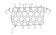
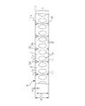
- FIG. 2 is a schematic sectional view taken along line II-II in FIG. 1.
- FIG. 3 is a schematic sectional view taken along line III-III in FIG. 1.
- the conductive film 10 embodying the present invention is formed in a mesh shape, and a plurality of openings as a mesh are arranged in a planar shape (two-dimensional).
- the conductive film 10 includes a film base 11 and a conductive material layer 12.
- the conductive material layer 12 is provided in a layered manner on one film substrate surface (hereinafter referred to as a first substrate surface) 11a of the film substrate 11, forms one film surface, and is a member formed of a conductive material.
- It is. 1 shows the conductive material layer 12 side of the conductive film 10, and in FIGS. 2 and 3, the thickness of the conductive material layer 12 is exaggerated with respect to the thickness of the film base 11. It is.
- the conductive film 10 When the conductive film 10 is attached to the object to be attached, the conductive film 10 is arranged so that the film base 11 is in contact with the object to be attached and the conductive material layer 12 is exposed to the outside.
- the thickness of the conductive film 10 is the sum of the thickness T11 of the film base 11 and the thickness T12 of the conductive material layer 12, and is denoted by reference numeral T10 in FIGS.
- a plurality of through holes 13 are formed through the film base material 11 and the conductive material layer 12 in a direction perpendicular to the film surface, that is, in the thickness direction.
- the plurality of through holes 13 are formed along the surface of the conductive material layer 12 as shown in FIG. 1, and are formed along the first substrate surface 11a in the film substrate 11 as shown in FIG. ing.
- These through-holes 13 are openings on the surface of the conductive material layer 12, the first base material surface 11a of the film base material 11, and the other film base material surface (hereinafter referred to as second base material surface) 11b, respectively. Is forming.
- the openings on the surface of the conductive material layer 12 are hereinafter referred to as layer openings and denoted by reference numerals 21a, 21b, 21c,... 21h,.
- the opening portion 11b is hereinafter referred to as a base material opening portion and denoted by reference numeral 11c.
- FIG. 1 only eight layer openings 21 a, 21 b,..., 21 h out of the layer openings 21 shown in FIG. When these are not distinguished, they are referred to as layer openings 21.
- Each diameter of the layer opening 21 and the substrate opening 11c in this embodiment is 5 ⁇ m.
- Each of the plurality of through holes 13 has a substantially constant size and shape, and when viewed from the direction perpendicular to the film surface on the conductive material layer 12 side, as shown in FIG.
- the through-holes 13 are densely arranged in a state in which the surrounding six through-holes 13 are arranged at the apexes of the hexagon centering on 13.
- the film substrate 11 has a mesh shape due to the plurality of through holes 13.
- the plurality of through holes 13 are preferably arranged regularly along the first base material surface 11a, and in this example, more specifically, are arranged in a matrix.
- the size and shape of the substrate opening 11c are substantially constant.
- Such a film substrate 11 has through-holes 13 in a manner similar to the above-described arrangement state on the film surface on the conductive material layer 12 side shown in FIG. 1 when viewed from the direction perpendicular to the first substrate surface 11a. Therefore, the film substrate 11 has a honeycomb structure, that is, a honeycomb structure. This “honeycomb structure” will be described later.
- the partition wall 16 between the adjacent through hole 13 and the through hole 13 is formed on each of the first base material surface 11 a and the second base material surface 11 b in the film base material 11. It is preferable that the thickness gradually decreases from the center toward the center in the thickness direction.
- the partition wall 16 has a partition wall opening 16 a formed substantially at the center in the thickness direction in the film base 11, and thereby through holes adjacent to each other through the partition wall 16. 13 are connected in the direction along the 1st substrate surface 11a inside the film substrate 11.
- the partition wall 16 may not be formed with the partition opening 16a, and in this case, the through holes 13 are individually independent.
- the shape of the base material opening 11c and / or the shape of the through hole 13 in the cross section parallel to the first base material surface 11a is not necessarily hexagonal.
- the shape of the base material opening 11c is circular.
- the base material opening 11c and the through holes 13 on the first base material surface 11a may be, for example, a rounded substantially hexagonal or substantially octagonal shape, and the honeycomb structure includes such an aspect.
- the honeycomb structure includes a structure in which the through holes 13 are connected to each other inside the film substrate 11 as in this example, in addition to the structure in which the through holes 13 are independent from each other. Furthermore, the arrangement of the through holes 13 is not limited to the above. Three to five or seven or more through holes 13 may be arranged around any one through hole 13, and the through holes 13 may be arranged in a square.
- the thickness T11 of the film substrate 11 is preferably in the range of 0.2 ⁇ m or more and 20 ⁇ m or less, and is 4 ⁇ m in this embodiment.
- the thickness T11 can be obtained by observing the cross-sectional shape with a scanning electron microscope and measuring it in the image. This method is also used in this embodiment.
- the thickness T11 is more preferably in the range of 0.5 ⁇ m to 15 ⁇ m, and still more preferably in the range of 1.0 ⁇ m to 10 ⁇ m.
- the film substrate 11 includes a hydrophobic polymer 52 (see FIG. 14) that is transparent, specifically, transmits visible light.
- the hydrophobic polymer 52 that transmits visible light with high transmittance include polylactic acid, polycaprolactone, polyglycolic acid, polydioxanone, polyhydroxybutyrate, polybutadiene, polyurethane, polystyrene, polymethyl methacrylate, polycarbonate, and repetition thereof.
- a copolymer containing units, a rubber polymer having stretchability and / or elasticity, and the like are preferable.
- the rubber-based polymer material include polybutadiene, polyisoprene, polydimethylsiloxane derivatives, polyisobutylene, and the like.
- polybutadiene is used as the hydrophobic polymer.
- the film substrate 11 may contain a surfactant (amphiphilic compound) as long as it is 10% by mass or less with respect to the mass of the film substrate 11.
- the film substrate 11 is formed of any one of polybutadiene, polyisoprene, a polydimethylsiloxane derivative, and polyisobutylene from the viewpoint of making the conductive film 10 more deformable and from the viewpoint of developing durability against repeated deformation. It is more preferable.
- the film base material 11 overlaps the conductive material layer 12 with the layer opening 21 in a non-blocking state, and the conductive material layer 12 is arranged on the film base material 11 with the base material opening portion 11c in a non-blocking state.
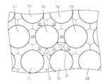
- the conductive material layer 12 has a plurality of conductive portions 22a, 22b,..., 22g,.
- the conductive portions 22a, 22b,..., 22g are denoted by reference numerals in order to avoid complication of the drawing.
- the conductive portion 22 exists linearly between the adjacent layer openings 21.
- the layer openings adjacent to the layer openings 21a are six layer openings denoted by reference numerals 21b to 21g, and each of these layer openings 21b to 21g and the layer openings.
- Conductive portions 22a to 22f exist between 21a.
- the centers of the plurality of layer openings 21 are connected by line segments, and when the line segments intersect, one short line
- the two layer openings 21 connected by the minute are defined as one “adjacent layer opening” of the two layer openings 21 connected by the other long line segment.
- the layer opening 21a and the layer opening The center of the opening 21h is connected by a line segment L1 indicated by a solid line, and the center of the layer opening 21b and the layer opening 21c is connected by a line segment L2 indicated by a broken line.
- the line segment L1 and the line segment L2 intersect, and the line segment L2 is shorter than the line segment L1. Accordingly, the layer opening adjacent to the layer opening 21a is the layer opening 21b and the layer opening 21c, and the layer opening 21h is not the layer opening adjacent to the layer opening 21a.
- Adjacent conductive portions 22 are connected to each other at the end portions, whereby a conductive path is formed in the surface direction of the conductive film 10.
- Reference numeral denotes a connection portion between the end portion of at least one conductive portion 22 and the end portion of at least one other conductive portion 22, that is, a connection point where the conductive portions 22 are connected to each other (hereinafter simply referred to as “connection point”). 23 is attached.
- Each of the layer openings 21 is surrounded by a plurality of conductive portions 22 connected to each other at the ends. In this example, when attention is paid to one layer opening 21a, the layer opening 21a has six conductive portions. Surrounded by the portions 22a to 22f. The three conductive portions 22 are connected at each connection point 23.
- the number of the conductive portions 22 is at least 400 per 1 mm 2 , that is, 400 or more. In this embodiment, the number is 42,000.
- the number of conductive portions 22 is more preferably in the range of 400 to 400,000, more preferably in the range of 1,000 to 200,000, more preferably 2000 to 100,000, per 1 mm 2 of area. It is particularly preferable that the value falls within the range.
- the number of the conductive portions 22 per area of 1 mm 2 can be obtained using, for example, an image with a general optical microscope.
- the conductive material layer 12 has an opening ratio of at least 40%, that is, 40% or more when the conductive film 10 is viewed from one film surface side on the conductive material layer 12 side. is there.
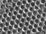
- This aperture ratio can be obtained by using an image with a scanning electron microscope. Specifically, when the image is rectangular, one side is x, the other side is y, the radius of the layer opening 21 is r, and the layer opening 21 in the area of the image (xy which is the product of x and y). Is the percentage obtained by the formula of ( ⁇ r 2 n / xy) ⁇ 100, where n is the number, and in this embodiment, it is obtained using the image of FIG.
- the aperture ratio of the conductive material layer 12 is more preferably in the range of 40% to 90%, further preferably in the range of 45% to 80%, and in the range of 50% to 70%. It is particularly preferred that
- the conductive material layer 12 may be formed on the surface of the partition wall 16 in addition to the first base material surface 11a. From the viewpoint of making the conductive film 10 more deformable, specifically, the conductive film 10 bends with a smaller curvature, grows with a larger elongation rate, and is bent and / or stretched to its original state. From the viewpoint of facilitating restoration, it is preferable that the conductive material layer 12 is not formed on the surface of the partition wall 16, and even if formed, the smaller the area, the better.
- the thickness T12 of the conductive material layer 12 has a slight difference in a preferable range depending on the conductive material constituting the conductive material layer 12.
- the thickness T12 is within a range of 10 nm to 50 nm. Preferably, it is 23.200 nm in this embodiment.
- the thickness T12 is more preferably in the range of 15 nm to 40 nm, and still more preferably in the range of 20 nm to 30 nm.
- the conductive film 10 was embedded in an epoxy resin, and a section was prepared with an ultramicrotome (UC6, Leica Microsystems), and a transmission electron microscope (H-7650, Hitachi, Ltd.) of the section was prepared. This method is also used in this embodiment. In the present embodiment, more specifically, after measuring the thickness at 10 points per section to obtain 10 measurement values, the average value of the 10 measurement values is set as the thickness T12.
- the conductive material constituting the conductive material layer 12 uses gold (Au) in this embodiment (see FIG. 6), but is not limited to this.
- gold Au
- titanium (Ti) see FIG. 7
- platinum ( Pt) see FIG. 8
- silver Ag
- copper copper
- Ni nickel
- palladium Pd
- the thickness T12 is formed to be the same, among the above-described conductive materials, from the viewpoint of expressing high conductivity and from the viewpoint of extending the conductive film 10 with a larger elongation rate and increasing durability against repeated deformation, Gold, titanium, and platinum are more preferable, and gold is particularly preferable among these.
- the conductive material layer 12 may be a member formed by a thermal evaporation method (hereinafter referred to as a thermal evaporation member), but is preferably a member formed by a sputtering method (hereinafter referred to as a sputter forming member). Also in the embodiment, a sputter forming member is used.
- the conductive material layer 12 is provided on the first substrate surface 11a of the film substrate 11 having a mesh-like structure, in this example, a honeycomb-like structure, and the opening ratio by the layer opening 21 is at least 40%. Therefore, the conductive film 10 exhibits high visible light transmittance (hereinafter simply referred to as transmittance).
- Table 1 shows the evaluation results of transmittance.
- the transmittance is measured using a spectrophotometer (V-670, JASCO Corporation) equipped with a detection unit with an integrating sphere. Specifically, it is obtained by subtracting the diffuse transmittance from 100% after obtaining the diffuse reflectance of each conductive film 10 in the wavelength range of 350 nm to 700 nm as the visible light region. As shown in Table 1, even when the thickness T12 of the conductive material layer 12 is increased, the conductive film 10 exhibits high transmittance. In Table 1, the case where “the thickness of the conductive material layer” is 0 nm is the transmittance of the film substrate 11 alone.
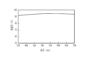
- the transmittance of the conductive film 10 is low in wavelength dependency of light, and as shown in FIG. 9, the transmittance is approximately 92% or more at a wavelength in the range of 350 nm to 700 nm.
- the transmittance (unit:%) with respect to the wavelength of light is measured using a spectrophotometer (V-670, JASCO Corporation) equipped with a detection unit with an integrating sphere. Specifically, after obtaining the diffuse reflectance of the conductive film 10 in the wavelength range from 350 nm to 700 nm, the diffuse transmittance is subtracted from 100%.
- the film substrate 11 is formed in a mesh shape by the plurality of through holes 13, the film substrate in which the through holes 13 are not formed, and the plurality of holes are formed in a state in which only one film substrate surface is opened.
- the film base is bent with a smaller curvature, and stretched with a larger elongation, It can be twisted, and is more easily restored from the bent state, the stretched state, and the twisted state to the original state.
- the conductive film 10 is deformable, and even if the surface shape is a curved surface, for example, the surface of a living tissue, the shape is changed so as to follow the shape, and the surface to be attached is, for example, dry. Also adheres to.
- the conductive film 10 is used by being attached, the conductive film 10 is deformed following the bending and / or expansion / contraction, twisting, etc. of the object to be attached, and also exhibits durability against repeated deformation.
- the through-hole 13 penetrates the film base material 11 in the thickness direction to form a base material opening 11c on the second base material surface 11b, and the second base material surface 11b excludes the base material opening 11c. Since the conductive film 10 is formed smoothly, the conductive film 10 is brought into close contact by the capillary force in the through hole 13 when the second base material surface 11b is placed in close contact with an object to be pasted containing a liquid such as water. Maintain state more reliably.
- the conductive film 10 Since the thickness of the partition wall 16 gradually decreases toward the center in the thickness direction of the film base material 11, the conductive film 10 is more deformable than in the case where it is constant in the thickness direction of the film base material 11. In addition, durability against repeated deformation is also superior. Since the partition film 16 has the partition opening 16a formed in the conductive film 10, the conductive film 10 is more deformable and more resistant to repeated deformation than those not formed.
- the plurality of through-holes 13 are regularly arranged along the first base material surface 11a, stress is uniformly applied in the surface direction of the film base material 11 when deformed, and local stress concentration is suppressed. Is done. For this reason, local stress concentration is also suppressed in the conductive material layer 12 on the first base material surface 11a, and the conductive path is held with higher accuracy during deformation. By holding this conductive path, the conductivity of the entire film surface of the conductive film 10 is secured. Therefore, the conductive film 10 is more reliably deformable and durable against repeated deformation, and this certainty is further enhanced by the film base 11 having a honeycomb structure.
- the conductive film 10 Since the thickness T11 of the film substrate 11 is 0.2 ⁇ m or more, the conductive film 10 has higher strength than the case where the thickness T11 is less than 0.2 ⁇ m, and does not break during expansion and contraction and has self-supporting properties. Since the thickness T11 is 20 ⁇ m or less, the shape is changed so as to conform to the surface shape of the object to be pasted, as compared with the case where the thickness T11 is larger than 20 ⁇ m. Hold more securely. And even if it is as thin as 20 micrometers or less, the electroconductive film 10 is hard to fracture
- the conductive material layer 12 is provided on the first substrate surface 11a of the film substrate 11, and the conductive film 10 exhibits conductivity in the surface direction by forming a conductive path by connecting the conductive portions 22 to each other. Conductivity over the entire film surface is developed. Since the number of conductive portions 22 connected at each connection point 23 is 3 in the present embodiment, a pair of conductive portions that are temporarily broken by the conductive film 10 or that are connected to each other due to deformation of the conductive film 10. Even if 22 are separated from each other, a conductive path is secured by the connection between the remaining conductive portions 22 and / or other conductive portions 22.
- the number of conductive portions 22 per 1 mm 2 of area is very large, at least 400, and the conductive portions 22 have a high density. Exists. Therefore, even if, for example, some of the conductive portions 22 are broken due to the deformation of the conductive film 10, a conductive path is ensured in the other conductive portions 22, and the conductivity is maintained.
- the thickness T12 of the conductive material layer 12 formed of gold (Au) is 10 nm or more, even when the conductive film 10 is deformed, the conductivity is more reliably maintained. Moreover, since thickness T12 is 50 nm or less, compared with the case where it is larger than 50 nm, even if the electroconductive film 10 is extended with a larger elongation rate, electroconductivity is hold
- the surface conductivity can be evaluated by sheet resistance.
- the sheet resistance is calculated by the formula R ⁇ w / L using the resistance value R of the conductive film 10 having a width of 1 cm and a length of 3 cm.
- the electric current is measured using an ALS electrochemical analyzer manufactured by BAS.
- the elongation rate is a value obtained by (L2 ⁇ L1) / L1, where L1 is the length before stretching and L2 is the length when stretched in one direction.
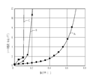
- the sheet resistance in FIG. 10 is calculated
- the gel member is polydimethylsiloxane (PDMS).
- PDMS polydimethylsiloxane
- Curve B (measured value is indicated by ⁇ ) in FIG. 10 is the sheet resistance when thickness T12 is 34.600 nm
- curve C (measured value is indicated by ⁇ ) is the sheet resistance when thickness T12 is 42.100 nm.
- the conductive portions 22 were broken at elongations of about 0.2 and about 0.1, respectively, and the sheet resistance was greatly increased. This is because the conductive material layer 12 becomes a hard film by increasing the thickness T12 and easily breaks with respect to elongation.
- the conductive material constituting the conductive material layer 12 is gold (Au)
- the conductivity with respect to the elongation can be changed by adjusting the thickness T12 according to the conductive material.
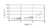
- the sheet resistance of the conductive film 10 hardly changes when the number of expansion and contraction is 100 or less, and is suppressed to about 2200 ⁇ / ⁇ even when the number of expansion and contraction is 1000.
- the elongation percentage indicated by ⁇ is 0.3, even if the number of expansions and contractions is 1000, it is suppressed to about 600 ⁇ / ⁇ .
- Each sheet resistance shown in FIG. 11 was measured in a state in which the stretching force was released in a predetermined direction and then the process of releasing the stretching force was repeated, the final stretching was finished and the stretching force was released. It is. ⁇ is when the elongation is 0.5, and ⁇ is when the elongation is 0.4.
- the sample used for the measurement is the same as the sample used for measuring the sheet resistance shown in FIG.
- the conductive material layer 12 is a sputter forming member (see FIG. 12), the thickness is more uniform over a wide range than, for example, a thermal evaporation member (see FIG. 13) or an electroless plating member formed by electroless plating. . For this reason, when the conductive film 10 is deformed, breakage of the conductive portion 22 and / or separation of the conductive portions 22 are more reliably suppressed. As shown in FIGS. 12 and 13, the sputter forming member is formed without more reliably closing the base material opening 11 c of the film base material 11 than the thermal evaporation member. More preferred.
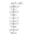
- the conductive film 10 is manufactured, for example, by a conductive film manufacturing process shown in FIG.
- the conductive film manufacturing process includes a solution preparation process 41, a casting process 42, a dew condensation process 43, an evaporation process 44, a peeling process 45, and a conductive material layer forming process 46.
- the solution preparation step 41 is a step of preparing a solution 51 for forming the film substrate 11.
- the hydrophobic polymer 52 is dissolved in a solvent 53 to form a solution 51.
- the casting step 42 is a step of forming the casting film 54 by spreading the solution 51 on a support (not shown). It is preferable that the temperature of the support is adjusted in advance, and the temperature is adjusted while the casting film 54 is formed.
- the solvent 53 is selected depending on the type of the hydrophobic polymer 52.
- hydrophobic polymers 52 for example, dichloromethane, chloroform, toluene, normal hexane can be used alone, or a plurality of types selected from these can be used in combination, and other liquids can be added. It may be used.
- chloroform can be used alone, or a mixture containing chloroform as a main component can be used.
- the condensation step 43 is a step of forming water droplets by condensation on the film surface of the casting film 54.
- the water droplets are formed by cooling the casting film 54 through the support so that the temperature is lower than the temperature of the surrounding atmosphere.
- the humidification was performed while adjusting the temperature of the support so that the support was maintained at a predetermined temperature. It is preferable to supply a gas (for example, air) onto the casting membrane 54.
- the evaporation step 44 is a step of evaporating the water droplets formed in the condensation step 43 and the solvent 53.
- the solvent 53 is evaporated faster than the water droplets.
- a water droplet is submerged in the casting film 54, and a hole is formed using the submerged water droplet as a mold. This hole becomes the through hole 13 in the obtained film substrate 11.
- the timing at which the water droplets start to evaporate may not be after all of the solvent 53 has been evaporated. Further, as long as the formed pores are maintained, some solvent 53 may remain in the casting film 54 even after the evaporation of water droplets is completed.
- the remaining solvent 53 is Evaporate after the evaporation of water droplets is complete.
- water droplets may start to sink into the casting film 54.
- the dew condensation process 43 and the evaporation process 44 are processes of a dew condensation method (also called a Breath- Figure method), which is well known as a method for producing a porous film having a honeycomb structure.
- the peeling process 45 the casting film 54 is peeled off from the support as the film base material 11.
- the conductive material layer 12 is formed on the first base material surface 11a of the film base material 11 peeled from the support.
- a thermal evaporation method and a sputtering method can be used, but the sputtering method is more preferable, and the sputtering method is also used in this embodiment.
- the film base material 11 may be used in the sputtering processing apparatus in a state where the film base 11 is held on a frame (frame member) provided with a jig for setting in the sputtering processing apparatus.
- the sputtering method when the partition wall 16 is gradually reduced toward the center in the thickness direction of the film substrate 11, the sputtering method has a conductive material on the surface of the partition wall 16 as compared with the thermal evaporation method. It is also preferable in that the layer 12 is not easily formed.
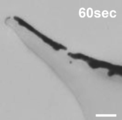
- the thickness T12 of the conductive material layer 12 can be changed by changing the sputtering time. As shown in Table 2, the thickness T12 can be increased as the sputtering time is increased. 15 and 16, it can be seen that the conductive material layer 12 having a sputtering time of 60 seconds is formed thicker than the conductive material layer 12 having a sputtering time of 20 seconds. 15 and 16 are cross-sectional images in the vicinity of the substrate opening 11c. The black portion is the conductive material layer 12, the lower left of each image is the inside of the through-hole 13 in the film substrate 11, and the upper right is the conductive material. It is an external space on the layer 12. 15 and FIG.
- the image is obtained by embedding the conductive film 10 in an epoxy resin, preparing a section with the aforementioned ultramicrotome, and observing the section with a transmission electron microscope (H-7650, manufactured by Hitachi, Ltd.). can get.
- the thickness T12 can be adjusted by adjusting at least one of the sputtering time and the distance between the metal target and the film substrate 11.
- a commercially available sputtering film forming apparatus may be used.
- a multi-target compact coater (SVC-700TMSG-NS, manufactured by Sanyu Electronics Co., Ltd.) is used.
- Sputtering in this embodiment is performed by setting the chamber internal pressure to 0.4 Pa, the applied DC voltage to the target metal to 320 V (current is 22 mA), and the distance between the target metal and the film substrate 11 to 5 cm.
- the conductive material layer forming step 46 is performed after the peeling step 45, but the peeling step 45 may be performed after the conductive material layer forming step 46.
- the aperture ratio of the conductive material layer 12 and the number of conductive portions 22 per area of 1 mm 2 can be changed by controlling the shape of the through holes 13 in the film substrate 11.
- the shape of the through hole 13 in the film substrate 11 can be controlled by the dew condensation process 43 and / or the evaporation process 44. It should be noted that paragraphs [0017] and [0018] of JP 2010-70648 A, paragraphs [0032] to [0040] of JP 2010-76105 A, paragraphs [0009] and [0040] of JP 2010-235808 A, respectively. 0025] and the like, it is described that the shape of the pores is controlled by controlling the temperature of the support and / or humidified gas, and the growth time of water droplets generated by condensation. The technique can be applied to the condensation step 43 and / or the evaporation step 44.
- the conductive film 10 of the embodiment is manufactured by the following method. First, a hydrophobic polymer 52 and an amphiphilic polymer compound as a surfactant are mixed at a mass ratio of 10: 1, and this mixture is dissolved in a solvent 53 to prepare a solution 51 having a concentration of 2 mg / ml. did.
- the cast film 54 was formed by applying this solution 51 to a glass plate as a support placed on a cooling plate. The cast film 54 was supplied with highly humidified air. At this time, the temperature of the cooling plate was adjusted to 10 ° C., and the humidity of the humidified air was adjusted so that the dew point was 18 ° C. The cast film 54 was dried and then peeled off from the glass plate to obtain the film substrate 11. As described above, the conductive material layer 12 was applied to the film base 11 using the sputtering method. Each diameter of the layer opening 21 and the substrate opening 11c, the opening ratio in the conductive material layer 12, the thickness T11 of the film substrate 11, and the number of the conductive portions 22 per 1 mm 2 were confirmed using a microscope.
- each diameter of the layer opening 21 and the base material opening 11c is 45 ⁇ m
- the opening ratio in the conductive material layer 12 is 60%
- the thickness T11 of the film base material 11 is 20 ⁇ m
- the number of the conductive parts 22 is More specifically, 480 conductive films 10 per 1 mm 2 are manufactured by the following method. First, the hydrophobic polymer 52 and the amphiphilic polymer compound as the surfactant are mixed at a mass ratio of 10: 1, and this mixture is dissolved in the solvent 53, so that the solution 51 in the above alternative embodiment is more than the solution 51. A high concentration solution 51 was prepared.
- the cast film 54 was formed by applying this solution 51 to a glass plate as a support placed on a cooling plate.
- the cast film 54 was supplied with highly humidified air. At this time, the temperature of the cooling plate was adjusted to 5 ° C., and the humidity of the humidified air was adjusted so that the dew point was 20 ° C.
- the cast film 54 was dried and then peeled off from the glass plate to obtain the film substrate 11.
- the conductive material layer 12 was applied to the film base 11 using the sputtering method. Each diameter of the layer opening 21 and the substrate opening 11c, the opening ratio in the conductive material layer 12, the thickness T11 of the film substrate 11, and the number of the conductive portions 22 per 1 mm 2 were confirmed using a microscope.
- a predetermined pattern may be formed on the conductive material layer 12.
- the conductive material layer 12 of the conductive film 10 obtained by the above method is subjected to patterning processing by so-called laser ablation to form an electrode pattern to produce an electrode material.
- the produced electrode material was placed on the convex surface of a soft contact lens in a water-containing state placed on a glass ball.
- the electrode material was approximately half the area of the soft contact lens, and was placed in one half area of the convex surface.
- the film substrate 11 was arranged so as to be in contact with the soft contact lens, the electrode material was in close contact with the soft contact lens.
- a conductive tester was fabricated by using an LED (Light Emitting Diode), a power source and a pair of terminals. This conductive tester can confirm energization by turning on the LED. With the electrode material in close contact with the soft contact lens, the terminal was brought into contact with one end and the other end of the electrode pattern, and energization was confirmed by lighting the LED. In order to confirm the energization, a 3V DC voltage is applied to light the LED.
- the conductive film 10 functions as an electrode material having one end connected to the anode and the other end connected to the cathode.
- the film base material is not limited to the film base material 11 having a honeycomb structure as long as it has a mesh shape.
- the mesh shape include a woven fabric shape, a knitted fabric shape, a non-woven fabric shape, and a sponge shape.
- the conductive film including the film base material and the conductive material layer in such a mode has the same function as the conductive film 10 described above. It has.
- Sponge means a porous shape in which a plurality of irregular voids are formed.
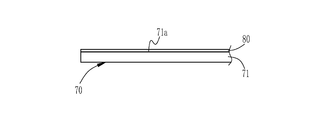
- a conductive film 70 shown in FIG. 17A includes a film base 71 and a conductive material layer 80.
- the conductive material layer 80 is provided on the first substrate surface 71a of the film substrate 71 in a layered manner.
- the conductive film 70 has a through-hole 75 (see FIG. 17B) penetrating the film base 71 and the conductive material layer 80 in the thickness direction. The illustration of the through hole 75 is omitted.
- FIG. 17A schematically shows the conductive film 70, and each film surface is drawn flat for convenience.
- the film base 71 includes a plurality of first linear bodies 72 extending in the first direction, and a plurality of second linear elements extending in the second direction orthogonal to the first direction. It is formed in a woven shape woven with the body 73.
- the 1st linear body 72 and the 2nd linear body 73 are formed with the above-mentioned hydrophobic polymer.
- the through-hole 75 surrounded by the first striate body 72 and the second striate body 73 forms a base material opening in each of the first base material surface 71a and the second base material surface 71b.
- the first striate body 72 and the second striatum body 73 are independent from each other, but may be integrated by, for example, fusion by heating. Moreover, the crossing angle of the 1st linear body 72 and the 2nd linear body 73 is not restricted to 90 degrees. In this example, the distance between the adjacent first filaments 72 is constant, and the distance between the adjacent second filaments 73 is also constant. Thereby, the plurality of through holes 75 are regularly arranged. However, at least one of the distance between the adjacent first linear bodies 72 and the distance between the adjacent second linear bodies 73 may be made non-uniform.
- this film substrate 71 is also formed in a mesh shape, as with the film substrate 11, a film substrate in which no through-hole is formed, and a plurality of holes are formed by opening only on one film substrate surface.
- the film base is bent with a smaller curvature, and stretched with a larger elongation, It can be twisted, and is more easily restored from the bent state, the stretched state, and the twisted state to the original state. Therefore, the conductive film 70 (see FIG. 17A) including the film base 71 and the conductive material layer 80 (see FIG. 17A) is freely deformable and has a curved surface shape such as a tissue surface of a living body, for example.
- the shape is changed so as to conform to the shape, and the surface is in close contact with, for example, a dry pasting object.
- the conductive film 70 is used by being attached, the conductive film 70 is deformed following the bending and / or expansion / contraction, twisting, etc. of the object to be attached, and exhibits durability against repeated deformation.
- the conductive material layer 80 includes the conductive portions 22 on the first base material surface 71a side surfaces of the first linear body 72 and the second linear body 73 surrounding each through hole 75, respectively.
- a plurality of layer openings 81a, 81b, 81c,... are formed.
- the conductive portion 22 exists linearly between the adjacent layer openings 81, and the adjacent layer openings 81 in this example are the column direction in which the layer openings are arranged (the vertical direction in FIG. 17C). It means the layer openings 81 adjacent in the row direction (lateral direction in FIG. 17C).
- each layer opening 81 is surrounded by four conductive portions 22.
- the aperture ratio of the conductive material layer 80 is at least 40%, and the conductive film 70 exhibits a high transmittance.
- four conductive portions 22 are connected at one connection point 23. Therefore, even if, for example, some of the conductive portions 22 are broken due to the deformation, a conductive path is secured in the other conductive portions 22 and the conductivity is maintained.
- the conductive material layer 80 has at least 400 conductive portions 22 per 1 mm 2 when viewed from one film surface side on the conductive material layer 80 side.
- the conductive portions 22 are formed with high density in the conductive material layer 12, even if some of the conductive portions 22 are broken due to deformation, for example, a conductive path is secured in the other conductive portions 22, Sex is preserved.
- a conductive film 90 according to the third embodiment will be described with reference to FIG.
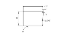
- the conductive film 90 includes a film substrate 11, a conductive material layer 12, and a gel layer 91.
- the gel layer 91 is disposed on the second substrate surface 11 b of the film substrate 11.
- the gel layer 91 covers the second base material surface 11b so as to close the base material opening 11c (not shown) formed in the second base material surface 11b.
- the gel layer 91 is for improving the adhesion to the object to be pasted. Therefore, when the conductive film 90 is attached to the object to be attached, the conductive film 90 is arranged so that the gel layer 91 is in contact with the object to be attached.
- the object to be pasted include those having a dry surface and / or a surface lacking adhesiveness and those having a surface that should be kept wet so as not to dry.
- a dry surface is a surface that does not contain a liquid such as water.
- the surface lacking adhesiveness is, for example, a surface having a fine concavo-convex structure in which a concave portion having a depth of about several ⁇ m and / or a convex portion having a height of about several ⁇ m is formed.
- the surface that should be kept wet so as not to be dried include the surface of a living tissue such as an eye.
- the gel layer 91 swells by absorbing a liquid such as water, and the constituent material is a gel.
- the gel layer 91 may be replaced with an elastomer layer 96 that uses an elastomer as a constituent material.
- a hydrogel composed of polyacrylamide and polyacrylamide-2-methylpropanesulfonic acid is preferable, and as the elastomer, for example, polydimethylsiloxane (PDMS) is preferable.
- a soft contact lens material is poly 2? Hydroxyethyl methacrylate (abbreviation: P-HEMA)
- P-HEMA Hydroxyethyl methacrylate
- the thickness TC of the gel layer 91 and the elastomer layer 96 is not particularly limited, and is, for example, in the range of 50 ⁇ m or more and 10 mm or less, and is 500 ⁇ m in this embodiment.
- the portion composed of the film base material 11 and the conductive material layer 12 can be deformed similarly to the conductive film 10 of the first embodiment and has durability against repeated deformation. Therefore, the gel layer 91 and the elastomer layer 96 is absorbed by the liquid and swells, or even if the gel layer 91 and the elastomer layer 96 are evaporated and contracted, the adhesion between the gel layer 91 or the elastomer layer 96 and the conductivity are Retained.
- the film substrate 11 of the conductive film 90 may be another mesh film substrate such as the film substrate 71.
- the conductive film 90 is manufactured by stacking the conductive film 10 and the gel layer 91 or the elastomer layer 96 in a swollen state containing liquid water. As described above, the base film opening 11 c is formed on the second base material surface 11 b and the film base material 11 is brought into close contact with the gel layer 91 or the elastomer layer 96 by the capillary force due to the through hole 13. Note that the conductive film 90 can be manufactured even when the gel layer or elastomer layer in a state of not containing the liquid and the conductive film 10 are overlapped and then the gel layer or elastomer layer absorbs the liquid.
- a predetermined pattern can also be formed on the conductive material layer 12 of the conductive film 90.
- the conductive material layer 12 of the conductive film 90 obtained by the above method is subjected to patterning processing by the laser ablation described above to form an electrode pattern to produce an electrode material.
- the conductive film 90 includes a gel layer 91, and the material thereof is a hydrogel made of polyacrylamide and polyacrylamide-2-methylpropanesulfonic acid.
- the produced electrode material was arranged on the peripheral surface of the pen. When the electrode material was arranged so that the gel layer 91 was in contact with the peripheral surface of the pen, the electrode material was in close contact with the pen.
- the pair of terminals of the conductive tester were brought into contact with one end and the other end of the electrode pattern, and energization was confirmed by lighting the LED. Further, when this electrode material was wound around a finger of a human hand, the electrode material was in close contact with the finger. The electrode material in close contact with the finger was confirmed to be energized by the conductive tester described above.
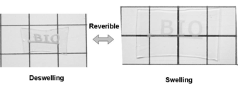
- the same electrode material is placed on a substrate on which a 1 cm square cell is drawn, and the swelling and drying of the gel layer 91 of the conductive film 90 are caused by absorption and evaporation of water. Repeated.
- a blackish part with the shape of the letters “B”, “I” and “O” arranged in one direction and a blackish line connecting these letters are formed by patterning.
- the conductive film 90 repeats a contracted state (left image) in which the gel layer 91 is in a dry state and an extended state (right image) in which the gel layer 91 is in a swollen state. . It can be seen that when the gel layer 91 is in a swollen state, the conductive film 90 is approximately twice as large as when it is in a dry state.
Landscapes
- Chemical & Material Sciences (AREA)
- Engineering & Computer Science (AREA)
- Medicinal Chemistry (AREA)
- Materials Engineering (AREA)
- Health & Medical Sciences (AREA)
- Chemical Kinetics & Catalysis (AREA)
- Polymers & Plastics (AREA)
- Organic Chemistry (AREA)
- Microelectronics & Electronic Packaging (AREA)
- Laminated Bodies (AREA)
- Coating Of Shaped Articles Made Of Macromolecular Substances (AREA)
- Manufacture Of Porous Articles, And Recovery And Treatment Of Waste Products (AREA)
- Physical Vapour Deposition (AREA)
- Shielding Devices Or Components To Electric Or Magnetic Fields (AREA)
- Non-Insulated Conductors (AREA)
Abstract
面方向における導電性を有し、変形自在で、耐久性に優れ、可視光を透過する導電性フィルムを提供する。 導電性フィルム(10,70,90)は、フィルム基材(11,71)と導電材料層(12,80)とを備える。導電材料層(12,80)は、フィルム基材(11,71)の第1基材面(11a,71a)に設けられている。導電性フィルム(10,70,90)には、フィルム基材(11,71)と導電材料層(12,80)とを厚み方向に貫通する貫通孔(13,75)が複数形成されている。導電材料層(12,80)は複数の導電部(22)を有し、各導電部(22)は隣り合う層開口部(21)の各間に存在する。導電部(22)の個数は1mm2当たり少なくとも400個であり、導電材料層(12,80)の開口率は少なくとも40%とされている。
Description
本発明は、導電性フィルムに関する。
生体の組織表面に対して非侵襲あるいは低侵襲な生体センサが要請されている。このような生体センサとして、血糖値または眼圧を検出するいわゆるスマートコンタクトレンズが提案されている。スマートコンタクトレンズのようなレンズ形態の生体センサでは、電極材として用いる導電性材料は可視光を透過することが望まれる。
可視光を透過する導電性材料は、これまで多く提案されている。例えば、特開平11-121974号公報には、透明な樹脂(ポリマー)基材と、この樹脂基材上に積層された金属薄膜からなる導電性メッシュとを備える電磁波遮蔽板としての、可視光を透過する導電性材料が記載されている。また、特開2014-175609号公報には、透明な樹脂基材と、この樹脂基材上に設けられ、複数の開口領域を画成する導電性メッシュとを備える、可視光を透過する導電性メッシュシートが記載されている。以上のような導電性材料における導電性メッシュは、網目としての開口領域を囲む複数の導電部から構成されており、導電部同士が互いの端部で接続されていることで導電パスを形成している。
また、組織表面のほとんどは球面などの曲面となっており、変形(例えば、曲がる、伸縮する、捻れる等)ことが通常である。したがって、組織表面に用いるための導電性材料には、曲面などにも沿うように変形することができる形状対応性、及び/または、例えば貼り付け対象物の変形に追従することができる変形追従性をもつことが要請される。こうしたいわゆる変形自在な導電性材料も、これまで提案されている。例えば特開2012-248346号公報に記載される導電性材料としての配線構造体は、生体の組織表面に貼り付ける生体センサに用いられ、基材としてのベース層と、導電層と、カバー層とを備える。ベース層は、柔軟性を有する樹脂素材、例えばポリジメチルシロキサンから形成されている。このベース層の表面には、断面形状が波状の凹凸部が形成されており、導電層はこの凹凸部上に設けられている。カバー層は、柔軟性を有する樹脂素材から形成され、導電層上に設けられている。
また、導電性材料としては、特開2011-216373号公報に記載されるように、表面が金属で被覆された樹脂繊維で形成された不織布もある。特開2007-073389号公報には、厚み方向に貫通した微小な孔がフィルム面に沿って複数並んで形成されることによりハニカム状の構造とされ、隣り合う孔と孔との間の隔壁の表面に無電解めっき層が形成されている導電性フィルムが記載されている。この導電性フィルムは、厚み方向にのみ導電性を示す異方性導電フィルムであり、個々の孔は独立している。
しかしながら、特開平11-121974号公報,特開2014-175609号公報,特開2011-216373号公報の各導電性材料は、多少は変形するものの、伸びたり曲げたりすることができる変形の程度は小さいので、変形自在とは言い難い。また、特開2012-248346号公報の導電性材料は、フィルム状ではあるものの、曲げ及び/または伸縮といった変形機能を発現ないし維持するために、基材であるベース層の厚みを300μmと厚くし、さらに導電層の上にカバー層を設けてあるので、材料としての厚みが大きい。このため用途が制限される。そして、特開2012-248346号公報の導電性材料は、導電性につき、繰り返しの変形に耐える一定の耐久性はもっているものの、耐えられる繰り返し回数は依然として少ない。また、特開2007-073389号公報の導電性材料は、フィルム面に沿ったいわゆる面方向には導電性がないので、前述の生体センサの電極材のような面方向に導電性が要求される用途には用いることができない。
そこで、本発明は、面方向における導電性を有し、変形自在で、耐久性に優れ、可視光を透過する導電性フィルムを提供することを目的とする。
上記課題を解決するために、本発明の導電性フィルムは、フィルム基材とフィルム基材の一方のフィルム基材面に配された導電材料層とを備え、フィルム基材及び導電材料層を厚み方向に貫通した複数の貫通孔が形成されている導電性フィルムであって、導電材料層は、互いに隣り合う開口部の各間に導電部を有し、導電部の個数が1mm2当たり少なくとも400個であり、導電材料層の開口率が少なくとも40%である。
フィルム基材の厚みは0.2μm以上20μm以下の範囲内であることが好ましい。フィルム基材は疎水性ポリマーを含むことが好ましい。疎水性ポリマーは、ポリブタジエン、ポリイソプレン、ポリジメチルシロキサン誘導体、またはポリイソブチレンのいずれかを含むことが好ましい。
複数の貫通孔は、一方のフィルム基材面に沿って規則的に配列されていることが好ましく、フィルム基材は、一方のフィルム基材面の垂直方向からみたときにハニカム状の構造とされていることがより好ましく、隣り合う貫通孔の間の隔壁は、フィルム基材の厚み方向における中央に向かって厚みが漸減していることがさらに好ましい。隔壁はフィルム基材の厚み方向における中央に隔壁開口部を有することが好ましい。
導電材料層は金で形成されており、導電材料層の厚みが10nm以上50nm以下の範囲内であることが好ましい。導電材料層は、スパッタリング法により形成された部材であることが好ましい。フィルム基材の他方のフィルム基材面に、ゲル層またはエラストマー層を備えていてもよい。
本発明によれば、面方向における導電性を有し、可視光を透過し、変形自在で、優れた耐久性を示す。
[第1実施形態]
図1~図3に示すように、本発明を実施した導電性フィルム10は、メッシュ状に形成されており、網目としての開口が面状(二次元)に複数並んでいる。導電性フィルム10は、フィルム基材11と、導電材料層12とを備える。導電材料層12は、フィルム基材11の一方のフィルム基材面(以下、第1基材面と称する)11aに層状に設けられて一方のフィルム面を成し、導電材料で形成された部材である。なお、図1には、導電性フィルム10の導電材料層12側を図示しており、図2,図3では、フィルム基材11の厚みに対して導電材料層12の厚みを誇張して描いてある。導電性フィルム10を貼り付け対象物に対して貼り付ける場合には、フィルム基材11が貼り付け対象物に接し、導電材料層12が外側に露呈するように、導電性フィルム10を配する。なお、導電性フィルム10の厚みは、フィルム基材11の厚みT11と導電材料層12の厚みT12との和であり、図2及び図3においては符号T10を付す。
図1~図3に示すように、本発明を実施した導電性フィルム10は、メッシュ状に形成されており、網目としての開口が面状(二次元)に複数並んでいる。導電性フィルム10は、フィルム基材11と、導電材料層12とを備える。導電材料層12は、フィルム基材11の一方のフィルム基材面(以下、第1基材面と称する)11aに層状に設けられて一方のフィルム面を成し、導電材料で形成された部材である。なお、図1には、導電性フィルム10の導電材料層12側を図示しており、図2,図3では、フィルム基材11の厚みに対して導電材料層12の厚みを誇張して描いてある。導電性フィルム10を貼り付け対象物に対して貼り付ける場合には、フィルム基材11が貼り付け対象物に接し、導電材料層12が外側に露呈するように、導電性フィルム10を配する。なお、導電性フィルム10の厚みは、フィルム基材11の厚みT11と導電材料層12の厚みT12との和であり、図2及び図3においては符号T10を付す。
導電性フィルム10には、フィルム基材11及び導電材料層12を、フィルム面に対して垂直な方向、すなわち厚み方向に貫通した貫通孔13が、複数形成されている。複数の貫通孔13は、図1に示すように導電材料層12の表面に沿って形成されており、図2に示すようにフィルム基材11においては第1基材面11aに沿って形成されている。これら貫通孔13は、導電材料層12の表面と、フィルム基材11の第1基材面11a及び他方のフィルム基材面(以下、第2基材面と称する)11bとに、それぞれ開口部を形成している。導電材料層12の表面の開口部を、以下、層開口部と称して符号21a,21b,21c,・・・21h,・・・を付し、第1基材面11a及び第2基材面11bの開口部を、以下、基材開口部と称して符号11cを付す。図1においては、図の煩雑化を避けるため、図示している層開口部21のうち、8つの層開口部21a,21b,・・・,21hのみ符号を付しており、以下の説明においてこれらを区別しない場合には層開口部21と称する。本実施形態における層開口部21と基材開口部11cとの各径は5μmである。
複数の貫通孔13は、その大きさ、形状がそれぞれ概ね一定であり、導電材料層12側のフィルム面の垂直な方向から見たときに、図1に示すように、任意の1つの貫通孔13を中心にした6角形の各頂点に周囲の6個の貫通孔13が配された状態に、貫通孔13は密に配列している。
フィルム基材11は、上記の複数の貫通孔13により、メッシュ状とされている。複数の貫通孔13は、第1基材面11aに沿って規則的に配列していることが好ましく、この例では、より具体的にはマトリクス状に、配列されている。基材開口部11cの大きさ、形状はそれぞれ概ね一定である。
このようなフィルム基材11は、第1基材面11aの垂直な方向から見たときに、図1に示す導電材料層12側のフィルム面における前述の配列状態と同様の態様で貫通孔13が形成されており、このため、フィルム基材11は、蜂の巣状、すなわちハニカム状の構造となっている。この「ハニカム状の構造」については後述する。
隣り合う貫通孔13と貫通孔13との間の隔壁16は、フィルム基材11において、図2、図3に示されるように、第1基材面11aと第2基材面11bとのそれぞれから厚み方向での中央に向かうに従い厚みが漸減していることが好ましい。
この例では、隔壁16は、図2に示すように、フィルム基材11において、厚み方向での概ね中央に隔壁開口部16aが形成されており、これにより、隔壁16を介して隣り合う貫通孔13同士はフィルム基材11の内部で第1基材面11aに沿った方向に繋がっている。ただし、隔壁16は、隔壁開口部16aが形成されていない場合もあり、その場合には貫通孔13は個々に独立している。
ハニカム状の構造とは、基材開口部11cの形状、及び/または貫通孔13の第1基材面11aに平行な断面における形状が6角形である必要はない。この例では、基材開口部11cの形状は円形となっている。第1基材面11aの単位面積当たりの貫通孔13の密度及び/または隣り合う貫通孔13同士の距離等に応じて、基材開口部11cと、第1基材面11aにおける貫通孔13との各形状は、例えば丸みを帯びた略6角形または略8角形等になる場合もあり、ハニカム状の構造とはこのような態様も含む。また、ハニカム状の構造は、貫通孔13が互いに独立している構造の他、この例のように隣り合う貫通孔13同士がフィルム基材11の内部で繋がっている構造をも含む。さらに、貫通孔13の配列は、上記のものに限定されない。任意の1つの貫通孔13の周囲に3~5個、あるいは7個以上の貫通孔13が配されてもよく、貫通孔13が正方配列されてもよい。
フィルム基材11の厚みT11は、0.2μm以上20μm以下の範囲内であることが好ましく、本実施形態では4μmとしている。厚みT11は、断面形状を走査型電子顕微鏡で観察し、その画像において測定することにより求めることができ、本実施形態でもこの方法を用いている。厚みT11は0.5μm以上15μmの範囲内であることがより好ましく、1.0μm以上10μm以下の範囲内であることがさらに好ましい。
フィルム基材11は、透明な、具体的には可視光を透過する疎水性ポリマー52(図14参照)を含む。可視光を高い透過率で透過する疎水性ポリマー52としては、ポリ乳酸、ポリカプロラクトン、ポリグリコール酸、ポリジオキサノン、ポリヒドロキシブチレート、ポリブタジエン、ポリウレタン、ポリスチレン、ポリメタクリル酸メチル、ポリカーボネート、およびこれらの繰り返し単位を含む共重合体、伸縮性及び/または弾性を有するゴム系ポリマー等が好ましい。ゴム系ポリマー素材としては、ポリブタジエン、ポリイソプレン、ポリジメチルシロキサン誘導体、ポリイソブチレンなどが挙げられる。本実施形態では疎水性ポリマーとしてポリブタジエンを用いている。なお、フィルム基材11には、界面活性剤(両親媒性化合物)を、フィルム基材11の質量に対して10質量%以下ならば含んでいてもよい。フィルム基材11は、導電性フィルム10をより変形自在にする観点と、繰り返しの変形に対する耐久性を発現する観点とではポリブタジエン、ポリイソプレン、ポリジメチルシロキサン誘導体、ポリイソブチレンのいずれかで形成されることがより好ましい。
フィルム基材11は層開口部21を非閉塞な状態に導電材料層12と重なっており、また、導電材料層12は、基材開口部11cを非閉塞な状態にフィルム基材11上に配されている。導電材料層12は、図4に示すように、導電材料で形成された複数の導電部22a,22b,・・・,22g,・・・を有する。なお、以降の説明において、導電部22a,22b,・・・,22g,・・・を区別しない場合には、導電部22と称する。図4においては、図の煩雑化を避けるため、図示している導電部22のうち、7つの導電部22a,22b,・・・,22gのみ符号を付してある。
導電部22は、導電性フィルム10を導電材料層12側のフィルム面の垂直な方向から見たときに、隣り合う層開口部21の各間に、線状に存在する。この例では、図4に示すように、層開口部21aに隣り合う層開口部は、符号21b~21gで示す6つの層開口部であり、これら層開口部21b~21gの各々と層開口部21aとの間に、導電部22a~22fが存在する。なお、導電材料層12側のフィルム面の垂直な方向から見たときに、複数の層開口部21の中心間を線分でそれぞれ結び、線分同士が交差する場合には、短い一方の線分で結んだ2つの層開口部21を、長い他方の線分で結んだ2つの層開口部21の一方の「隣り合う層開口部」とする。例えば、層開口部21aに対して層開口部21b,21c,21hのいずれが隣り合う層開口部であるかを判断する場合には、図5に示すように、まず、層開口部21aと層開口部21hとの中心間を実線で示す線分L1で結び、層開口部21bと層開口部21cとの中心間を破線で示す線分L2で結ぶ。線分L1と線分L2とは交差しており、線分L2は線分L1より短い。したがって、層開口部21aと隣り合う層開口部は、層開口部21bと層開口部21cとであり、層開口部21hは層開口部21aと隣り合う層開口部ではない、とする。
隣り合う導電部22は互いに端部で接続されており、これにより、導電性フィルム10の面方向で導電パスが形成される。少なくとも1つの導電部22の端部と他の少なくとも1つの導電部22の端部との接続部分、すなわち導電部22同士が接続する接続点(以下、単に「接続点」と称する)には符号23を付す。層開口部21の各々は、互いに端部で接続する複数の導電部22で囲まれており、この例では、ひとつの層開口部21aに着目した場合に、この層開口部21aは6つの導電部22a~22fに囲まれている。そして、各接続点23で3つの導電部22が接続している。
導電材料層12は、導電性フィルム10を導電材料層12側の一方のフィルム面側からみたときに、導電部22の個数が、面積1mm2当たり、少なくとも400個、すなわち400個以上とされており、本実施形態では42000個である。導電部22の個数は、面積1mm2当たり、400個以上400000個以下の範囲内であることがより好ましく、1000個以上200000個以下の範囲内であることがさらに好ましく、2000個以上100000個以下の範囲内であることが特に好ましい。面積1mm2当たりの導電部22の個数は、例えば、一般の光学顕微鏡での画像を用いて求めることができる。
導電材料層12は、導電性フィルム10を導電材料層12側の一方のフィルム面側からみたときに、開口率が少なくとも40%、すなわち40%以上とされており、本実施形態では70%である。この開口率は、走査型電子顕微鏡での画像を用いて求めることができる。具体的には、その画像が長方形であるときの一辺をx、他辺をy、層開口部21の半径をr、画像の面積(xとyとの積であるxy)における層開口部21の個数をn(個)とするときに、(πr2n/xy)×100の式で求められる百分率であり、本実施形態では後述の図12の画像を用いて求めている。導電材料層12の開口率は、40%以上90%以下の範囲内であることがより好ましく、45%以上80%以下の範囲内であることがさらに好ましく、50%以上70%以下の範囲内であることが特に好ましい。
導電材料層12は第1基材面11aに加えて隔壁16の表面にも形成されていてよい。導電性フィルム10をより変形自在にする観点、具体的には、導電性フィルム10がより小さい曲率で曲がり、より大きな伸び率で伸び、また、曲がった状態及び/または伸びた状態から元の状態へより復元しやすくなる観点から、導電材料層12は隔壁16の表面には形成されていない方が好ましく、形成されていても面積が小さいほど好ましい。
導電材料層12の厚みT12は、導電材料層12を構成する導電材料によって好ましい範囲に多少の違いがあり、後述のように金(Au)である場合には、10nm以上50nm以下の範囲内であることが好ましく、本実施形態では23.200nmにしてある。厚みT12は、15nm以上40nm以下の範囲内であることがより好ましく、20nm以上30nm以下の範囲内であることがさらに好ましい。厚みT12は、導電性フィルム10をエポキシ樹脂に包埋し、ウルトラミクロトーム(UC6、ライカマイクロシステムズ(株))で切片を作製し、この切片の透過型電子顕微鏡(H-7650、(株)日立製作所製)での画像により求めることができ、本実施形態でもこの方法を用いている。本実施形態においては、より具体的には、切片につき10箇所で厚みを測定して10個の測定値を得た後に、それら10個の測定値の平均値を厚みT12としている。
導電材料層12を構成する導電材料は、本実施形態では金(Au)を用いている(図6参照)が、これに限定されず、例えば、チタン(Ti)(図7参照)、白金(Pt)(図8参照)、銀(Ag)、銅(Cu)、ニッケル(Ni)、パラジウム(Pd)等でもよい。厚みT12を同じに形成した場合において、高い導電性を発現する観点と、導電性フィルム10をより大きな伸び率で延ばしたり、繰り返しの変形に対する耐久性を高める観点とから、上記の導電材料の中でも金、チタン、白金がより好ましく、これらの中でも金が特に好ましい。
導電材料層12は、熱蒸着法により形成された部材(以下、熱蒸着部材と称する)でもよいが、スパッタリング法により形成された部材(以下、スパッタ形成部材と称する)である方が好ましく、本実施形態でもスパッタ形成部材としている。
上記構成の作用を説明する。導電材料層12は、メッシュ状、この例ではハニカム状の構造をもつフィルム基材11の第1基材面11a上に設けられており、層開口部21による開口率が少なくとも40%とされているから、導電性フィルム10は可視光の高い透過率(以下、単に透過率と称する)を示す。
透過率の評価結果を表1に示す。透過率は、積分球付き検出ユニットを搭載した分光光度計(V-670、日本分光(株))を用いて測定している。具体的には、可視光域としての350nmから700nmの波長域に関して各導電性フィルム10の拡散反射率を求めた後、100%から拡散透過率を減算することで求めている。表1に示すように、導電材料層12の厚みT12が厚くなっても、導電性フィルム10は、高い透過率を示す。表1において、「導電材料層の厚み」が0nmである場合が、フィルム基材11単体での透過率である。

また、導電性フィルム10の透過率は、光の波長依存性が低く、図9に示すように、350nm以上700nm以下の範囲内の波長において、概ね92%以上の透過率を示す。本実施形態においては、光の波長に対する透過率(単位は%)は、積分球付き検出ユニットを搭載した分光光度計(V-670、日本分光(株))を用いて測定している。具体的には、350nmから700nmの波長域に関して導電性フィルム10の拡散反射率を求めた後、100%から拡散透過率を減算して求めている。
フィルム基材11は、複数の貫通孔13によりメッシュ状に形成されているから、貫通孔13が形成されていないフィルム基材、複数の孔が一方のフィルム基材面にのみ開口した状態に形成されているフィルム基材、複数の孔が両フィルム基材面に開口しておらず内部に空隙として封じられているフィルム基材に比べて、より小さい曲率で曲がり、より大きな伸び率で伸び、捻れることができ、また、曲がった状態、伸びた状態、捻れた状態から元の状態へより復元しやすい。そのため、導電性フィルム10は、変形自在であって、例えば生体の組織表面などのように表面形状が曲面であってもその形状に沿うように形を変え、表面が例えば乾いた貼り付け対象物に対しても密着する。また、導電性フィルム10は、貼り付けて用いた場合に貼り付け対象物の曲げ及び/または伸縮、捻じれなどに追従して変形し、繰り返しの変形に対する耐久性も示す。
さらに、貫通孔13はフィルム基材11を厚み方向に貫通して第2基材面11bに基材開口部11cを形成しており、第2基材面11bは基材開口部11cを除いて平滑に形成されているから、導電性フィルム10は、例えば水などの液体を含む貼り付け対象物に第2基材面11bを密着して配した際に、貫通孔13における毛管力によって、密着状態をより確実に保持する。
隔壁16の厚みは、フィルム基材11の厚み方向での中央に向かうに従い漸減しているから、フィルム基材11の厚み方向において一定である場合に比べて、導電性フィルム10はより変形自在であり、繰り返しの変形に対する耐久性もより優れる。導電性フィルム10は、隔壁16に隔壁開口部16aが形成されているから、形成されていないものに比べて、より変形自在であり、繰り返しの変形に対する耐久性もより優れる。
複数の貫通孔13は、第1基材面11aに沿って規則的に配列しているから、変形した際に応力がフィルム基材11の面方向で均一にかかり、局部的な応力集中が抑制される。このため、第1基材面11a上の導電材料層12においても局部的な応力集中が抑制されて、変形の際に、より高い確度で導電パスが保持される。この導電パスの保持により、導電性フィルム10のフィルム面全体での導電性が担保される。したがって、導電性フィルム10は、変形自在な性質と繰り返しの変形に対する耐久性とがより確実になり、この確実性は、フィルム基材11がハニカム状の構造とされることでより高まる。
フィルム基材11の厚みT11が0.2μm以上であるから、0.2μm未満である場合に比べて、導電性フィルム10は高い強度をもち、伸縮変形時に破断せず、自己支持性を有する。厚みT11が20μm以下であるから、20μmより大きい場合に比べて、貼り付け対象物の表面形状に沿うように形を変え、また、貼り付け対象物の表面形状の変形に追従して、密着状態をより確実に保持する。そして、20μm以下という薄さであっても、導電性フィルム10は、フィルム基材11の上記構成により、変形しても破断しにくく、また、繰り返しの変形に対する耐久性も示す。
導電材料層12はフィルム基材11の第1基材面11a上に設けられており、導電部22同士の接続による導電パスの形成により、導電性フィルム10は面方向での導電性を示し、フィルム面全域に亘る導電性が発現する。各接続点23で接続する導電部22の個数は本実施形態では3とされているから、導電性フィルム10の変形で、仮にひとつの導電部22が破断したり、互いに接続する一対の導電部22同士が離れても、残りの導電部22及び/または他の導電部22同士の接続によって導電パスが確保される。そして、導電性フィルム10を導電材料層12側の一方のフィルム面側からみたときに、面積1mm2当たりの導電部22の個数は、少なくとも400個と非常に多く、導電部22が高密度に存在する。そのため、導電性フィルム10の変形で例えばいくつかの導電部22が破断しても、他の導電部22で導電パスが確保され、導電性が保持される。
金(Au)で形成されている導電材料層12の厚みT12は、10nm以上であるから、導電性フィルム10が変形しても、より確実に導電性が保持される。また、厚みT12が50nm以下であるから、50nmよりも大きい場合に比べて、導電性フィルム10がより大きな伸び率で延ばされても、導電性がより確実に保持される。
面方向の導電性は、シート抵抗によって評価することができる。本実施形態では、シート抵抗は、幅が1cm、長さが3cmの導電性フィルム10の抵抗値Rを用い、R×w/Lの式により算出している。導電性フィルム10の抵抗値Rは、上記サイズの導電性フィルム10の長手方向における両端に1Vの定電圧を印加し、印加中に流れる電流を計測し、オームの法則(V=IR)より算出している。電流は、ビー・エー・エス(株)製のALS電気化学アナライザを用いて計測している。伸び率は、伸ばす前の状態の長さをL1、一方向に伸ばした状態の長さをL2とするときに、(L2-L1)/L1で求める値である。導電材料層12の厚みT12が23.200nmである本実施形態の導電性フィルム10のシート抵抗は、図10の曲線A(測定値は●で示してある)で示すように、伸び率が0.2以下ではほとんど変化せず、伸び率が0.6であっても6kΩ/□よりも小さく抑えられている。なお、図10におけるシート抵抗は、伸び率が0である場合を除いて、いずれも伸ばした状態で求めており、測定に用いたサンプルは、導電性フィルム10のフィルム基材11の第2基材面11bに厚みが500μmのゲル部材を備えたものとしている。ゲル部材は、ポリジメチルシロキサン(PDMS)である。また、上記のように本明細書でのシート抵抗の単位として用いている「kΩ/□」は、「kΩ/square」を意味しており、SI単位系では「kΩ」である。
なお、導電材料層12の厚みT12によって、伸び率に対して保持される導電性の程度は異なる。図10の曲線B(測定値は▲で示す)は厚みT12が34.600nm、曲線C(測定値は■で示す)は厚みT12が42.100nmの場合のシート抵抗である。それぞれ約0.2、約0.1の伸び率で導電部22が破断し、シート抵抗が大きく増加した。これは導電材料層12が厚みT12を増すことで硬い膜状となり伸びに対して破断しやすくなったためである。導電材料層12を構成する導電材料が金(Au)である場合において、10nm以上50nm以下の範囲内で厚みT12が薄いほど伸び率に対する導電性が優れる。このように、伸び率に対する導電性は、導電材料に応じて厚みT12を調整することで、変えることができる。
導電性フィルム10のシート抵抗は、図11に示すように、伸縮回数が100回以下ではほとんど変化せず、伸縮回数が1000回とされても2200Ω/□程度に抑えられている。特に、▲で示す伸び率が0.3の場合においては伸縮回数が1000回とされても600Ω/□程度に抑えられている。この図11に示す各シート抵抗は、所定の一方向に所定の伸び率で延伸した後、その延伸力を解除する処理を繰り返し、最終の延伸を終えて延伸力を解除した状態で測定したものである。◆は伸び率を0.5にした場合であり、■は伸び率を0.4にした場合である。測定に用いたサンプルは、図10に示すシート抵抗を測定するために用いたサンプルと同じ態様のものである。
導電材料層12は、スパッタ形成部材である(図12参照)ので、例えば熱蒸着部材(図13参照)または無電解めっきで形成された無電解めっき部材よりも、広範囲にわたって厚みがより均一である。このため、導電性フィルム10の変形の際に、導電部22の破断、及び/または導電部22同士が離れてしまうこと等が、より確実に抑制される。図12及び図13に示すように、スパッタ形成部材とすることで熱蒸着部材であるよりも、フィルム基材11の基材開口部11cをより確実に閉塞せずに形成されている点で、より好ましい。
導電性フィルム10は、例えば図14に示す導電性フィルム製造工程により製造される。導電性フィルム製造工程は、溶液調製工程41、流延工程42、結露工程43、蒸発工程44、剥離工程45、導電材料層形成工程46とを有する。
溶液調製工程41は、フィルム基材11を形成するための溶液51を調製する工程である。この例では、疎水性ポリマー52を、溶媒53に溶解して溶液51とする。流延工程42は、溶液51を支持体(図示無し)の上に流下して広げ、流延膜54を形成する工程である。支持体は、予め温度を調整しておき、流延膜54を形成する間も温度を調整していることが好ましい。なお、溶媒53は、疎水性ポリマー52の種類によって選定する。前述の各種疎水性ポリマー52を用いる場合には、例えば、ジクロロメタン、クロロホルム、トルエン、ノルマルヘキサンを単独で用いたり、またはこれらから選ばれる複数種類を併用することができ、さらに他の液体を加えて用いてもよい。疎水性ポリマー52として例えばポリブタジエンを用いる場合の溶媒53としては、クロロホルムを単独で用いたり、またはクロロホルムを主成分とする混合物を用いることができる。
結露工程43は、流延膜54の膜面に結露させて水滴を形成する工程である。水滴は、周辺の雰囲気の温度よりも低い温度となるように支持体を介して流延膜54を冷却することで形成される。ただし、複数の水滴の発生のタイミングを揃えたり、形成される水滴の大きさを均一に揃える観点では、支持体が所定の温度に保持されるように支持体の温度を調整しつつ、加湿した気体(例えば空気)を流延膜54上に供給することが好ましい。
蒸発工程44は、結露工程43で形成した水滴と、溶媒53とを蒸発させる工程である。この蒸発工程44では、水滴よりも溶媒53を早く蒸発させる。これにより、流延膜54中に水滴を沈み込ませ、沈み込んだ水滴を鋳型にして孔を形成する。この孔は、得られるフィルム基材11における貫通孔13となる。このため、溶媒53としては、水よりも蒸発速度が大きいものを用いることが好ましい。ただし、水滴が蒸発し始めるタイミングは、溶媒53のすべてが蒸発し終わった後でなくてもよい。また、形成された孔が維持される程度であれば、水滴の蒸発が完了した後にも多少の溶媒53が流延膜54に残っていてもよく、この場合には残存している溶媒53は水滴の蒸発が完了した後に蒸発させる。なお、結露工程43中に、水滴が流延膜54中に沈み込みを開始する場合もある。また、上記の結露工程43、蒸発工程44は、ハニカム状の構造をもつ多孔フィルムの製造方法として周知である、結露法(Breath Figure法とも呼ばれる)の工程である。剥離工程45では、支持体から流延膜54をフィルム基材11として剥がす。
導電材料層形成工程46は、支持体から剥離したフィルム基材11の第1基材面11aに導電材料層12を形成する。この導電材料層12の形成手法は、熱蒸着法とスパッタリング法とを用いることができるが、スパッタリング法の方がより好ましく、本実施形態でもスパッタリング法としている。スパッタリング法においては、例えば、フィルム基材11を、スパッタリング処理装置にセットするための治具を備えたフレーム(枠部材)に保持した状態で、スパッタリング処理装置に供するとよい。なお、本実施形態のように、隔壁16がフィルム基材11の厚み方向の中央に向かうに従い漸減している場合には、スパッタリング法は、熱蒸着法に比べて、隔壁16の表面に導電材料層12が形成されにくい点でも、好ましい。
スパッタリング法によって導電材料層12を形成する場合には、スパッタリング時間を変えることにより、導電材料層12の厚みT12を変えることができる。表2に示すように、スパッタリング時間を長くするほど、厚みT12を厚くすることができる。図15と図16とを比較すると、スパッタリング時間を20秒にした導電材料層12よりもスパッタリング時間を60秒にした導電材料層12の方が、厚く形成されていることがわかる。なお、図15及び図16は、基材開口部11c近傍における断面の画像であり、黒い部分が導電材料層12、各画像の左下はフィルム基材11における貫通孔13の内部、右上が導電材料層12上の外部空間である。図15と図16とは拡大倍率が互いに等しく、図16における右下の白い線分の長さは、図15におけるのと同じく100nmに相当する。画像は、導電性フィルム10をエポキシ樹脂に包埋して、前述のウルトラミクロトームで切片を作製し、この切片を透過型電子顕微鏡(H-7650、(株)日立製作所製)で観察することにより得られる。なお、スパッタリング時間と、金属ターゲットとフィルム基材11との距離との少なくともいずれか一方を調節することにより、厚みT12を調整することが可能である。
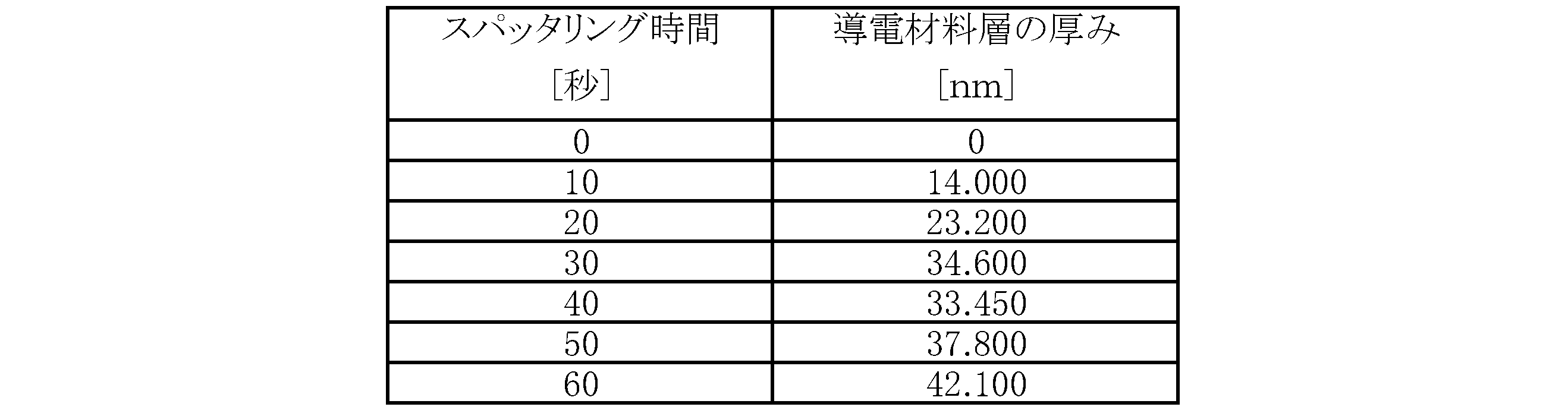
導電材料層12のスパッタリング法による形成には、市販のスパッタリング成膜装置を用いてよい。本実施形態では、マルチターゲットコンパクトコーター(SVC-700TMSG-NS、サンユー電子(株)製)を用いている。本実施形態におけるスパッタリングは、チャンバ内圧力を0.4Pa、ターゲット金属への印加直流電圧を320V(電流は22mA)、ターゲット金属とフィルム基材11との距離を5cmに設定して行っている。
上記の例では、導電材料層形成工程46を剥離工程45の後にしているが、剥離工程45を導電材料層形成工程46の後にしてもよい。
導電材料層12の開口率と面積1mm2当たりの導電部22の個数は、フィルム基材11における貫通孔13の形状を制御することにより変えられる。フィルム基材11における貫通孔13の形状は、結露工程43及び/または蒸発工程44で制御することができる。なお、特開2010-70648号公報の段落[0017],[0018]、特開2010-76105号公報の段落[0032]~[0040]、特開2010-235808号公報の段落[0009],[0025]等に、支持体及び/または加湿した気体などの各温度、結露で生成した水滴の成長時間を制御することで、孔の形状を制御することが記載されており、これらに記載される手法を、結露工程43及び/または蒸発工程44に適用することができる。
層開口部21及び基材開口部11cの各径が5μm、導電材料層12における開口率が70%、フィルム基材11の厚みT11が4μm、導電部22の個数が1mm2当たり42000個の本実施形態の導電性フィルム10は、より具体的には以下の方法で製造している。まず、疎水性ポリマー52と界面活性剤としての両親媒性高分子化合物とを、質量比10:1で混合し、この混合物を溶媒53に溶解して、濃度が2mg/ミリリットルの溶液51を調製した。疎水性ポリマー52としてはポリブタジエン(JSR株式会社製)を、溶媒53としてはクロロホルムを用いており、両親媒性高分子化合物は式(1)で示す両親媒性ポリアクリルアミドである。この溶液51を、冷却板上に設置した支持体としてのガラス板に塗布することで流延膜54を形成した。この流延膜54に、高加湿にされた空気を供給した。この際、冷却板の温度は10℃に、加湿した空気の湿度は露点が18℃になるように、それぞれ調節した。流延膜54を乾燥してからガラス板から剥ぎ取り、フィルム基材11を得た。このフィルム基材11に対して、前述のようにスパッタリング法を用いて導電材料層12を付与した。層開口部21及び基材開口部11cの各径、導電材料層12における開口率、フィルム基材11の厚みT11、1mm2当たりの導電部22の個数は顕微鏡を用いて確認した。
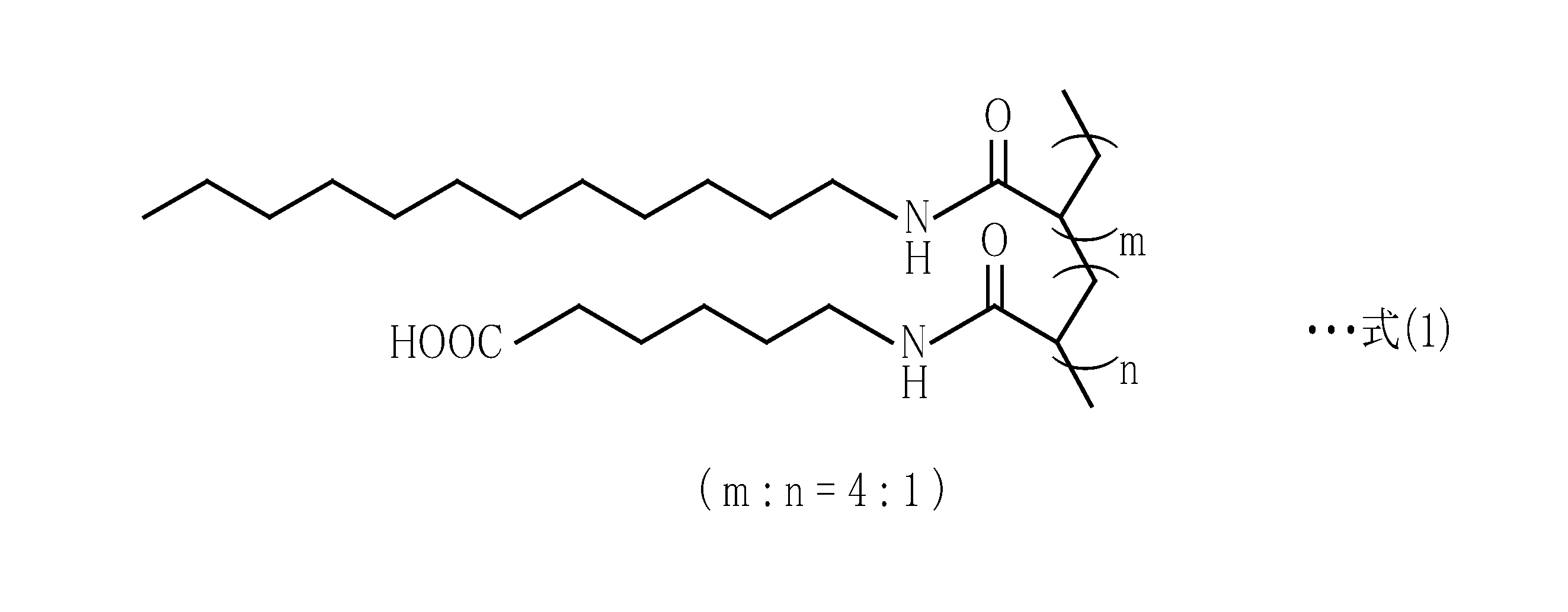
また、別の態様として、層開口部21及び基材開口部11cの各径が45μm、導電材料層12における開口率が60%、フィルム基材11の厚みT11が20μm、導電部22の個数が1mm2当たり480個の導電性フィルム10は、より具体的には以下の方法で製造している。まず、疎水性ポリマー52と界面活性剤としての両親媒性高分子化合物とを、質量比10:1で混合し、この混合物を溶媒53に溶解して、上記の別態様での溶液51よりも高い濃度の溶液51を調製した。疎水性ポリマー52としてはポリブタジエン(JSR株式会社製)を用い、溶媒53の主成分はクロロホルムとした。この溶液51を、冷却板上に設置した支持体としてのガラス板に塗布することで流延膜54を形成した。この流延膜54に、高加湿にされた空気を供給した。この際、冷却板の温度は5℃に、加湿した空気の湿度は露点が20℃になるように、それぞれ調節した。流延膜54を乾燥してからガラス板から剥ぎ取り、フィルム基材11を得た。このフィルム基材11に対して、前述のようにスパッタリング法を用いて導電材料層12を付与した。層開口部21及び基材開口部11cの各径、導電材料層12における開口率、フィルム基材11の厚みT11、1mm2当たりの導電部22の個数は顕微鏡を用いて確認した。
導電性フィルム10を例えば電極材として用いるために、導電材料層12に所定のパターンを形成してもよい。本実施形態では、上記の方法で得られた導電性フィルム10の導電材料層12に対し、いわゆるレーザーアブレーションによりパターニング処理を行い、電極パターンを形成して電極材を作製している。作製した電極材を、ガラス玉上に載置した含水状態のソフトコンタクトレンズの凸側表面に配した。電極材は、ソフトコンタクトレンズの概ね半分の面積とし、凸側表面の片側半分の領域に配した。フィルム基材11がソフトコンタクトレンズに接するように配したところ、電極材はソフトコンタクトレンズに密着した。LED(Light Emitting Diode)と電源と一対の端子とにより、導電テスタを作製した。この導電テスタは、LEDの点灯により通電を確認することができるものである。上記の電極材をソフトコンタクトレンズに密着させた状態で、電極パターンの一端と他端とにそれぞれ端子を接触させ、LEDの点灯によって、通電が確認された。なお、この通電の確認には、3Vの直流電圧を印加してLEDを点灯させている。このように、導電性フィルム10は、一端が陽極に接続され、他端が陰極に接続される電極材として機能する。
フィルム基材はメッシュ状であればハニカム状の構造のフィルム基材11に限定されない。メッシュ状としては、例えば織物状、編み物状、不織布状、スポンジ状などがあり、このような態様のフィルム基材と導電材料層とを備える導電性フィルムは上記の導電性フィルム10と同様の作用をもつ。なお、スポンジ状とは、不定形の空隙が複数形成されている多孔質状を意味する。
[第2実施形態]
図17Aに示す導電性フィルム70は、フィルム基材71と、導電材料層80とを備える。導電材料層80は、フィルム基材71の第1基材面71a上に、層状に重ねて設けられている。この導電性フィルム70にも導電性フィルム10と同様に、フィルム基材71と導電材料層80とを、厚み方向に貫通する貫通孔75(図17B参照)が形成されているが、図17Aにおいては貫通孔75の図示を略してある。なお、図17Aは、導電性フィルム70を模式的に示すものであり、各フィルム面を便宜的に平坦に描いてある。
図17Aに示す導電性フィルム70は、フィルム基材71と、導電材料層80とを備える。導電材料層80は、フィルム基材71の第1基材面71a上に、層状に重ねて設けられている。この導電性フィルム70にも導電性フィルム10と同様に、フィルム基材71と導電材料層80とを、厚み方向に貫通する貫通孔75(図17B参照)が形成されているが、図17Aにおいては貫通孔75の図示を略してある。なお、図17Aは、導電性フィルム70を模式的に示すものであり、各フィルム面を便宜的に平坦に描いてある。
フィルム基材71は、図17Bに示すように、第1の方向に延びた複数の第1線条体72と、第1の方向と直交する第2の方向に延びた複数の第2線条体73とで織られた織物状に形成されている。第1線条体72と第2線条体73とは、前述の疎水性ポリマーにより形成されている。第1線条体72と第2線条体73とに囲まれた貫通孔75は、第1基材面71aと第2基材面71bとのそれぞれに基材開口部を形成している。
第1線条体72と第2線条体73とは、互いに独立しているが、例えば加熱による融着などで一体にされていてもよい。また、第1線条体72と第2線条体73との交差角度は90°に限られない。隣り合う第1線条体72の間の距離を、この例では一定にし、隣り合う第2線条体73の間の距離も同様に一定にしている。これにより複数の貫通孔75は規則的に配列している。ただし、隣り合う第1線条体72の間の距離と、隣り合う第2線条体73の間の距離との少なくともいずれか一方を不均一にしてもよい。
このフィルム基材71もメッシュ状に形成されているから、フィルム基材11と同様に、貫通孔が形成されていないフィルム基材、複数の孔が一方のフィルム基材面にのみ開口して形成されているフィルム基材、複数の孔が両フィルム基材面に開口しておらず内部に空隙として封じられているフィルム基材に比べて、より小さい曲率で曲がり、より大きな伸び率で伸び、捻れることができ、また、曲がった状態、伸びた状態、捻れた状態から元の状態へより復元しやすい。そのため、このフィルム基材71と導電材料層80(図17A参照)とを備える導電性フィルム70(図17A参照)は、変形自在であって、例えば生体の組織表面などのように表面形状が曲面であってもその形状に沿うように形を変え、表面が例えば乾いた貼り付け対象物に対しても密着する。また、この導電性フィルム70は、貼り付けて用いた場合に貼り付け対象物の曲げ及び/または伸縮、捻じれなどに追従して変形し、繰り返しの変形に対する耐久性も示す。
導電材料層80は、図17Cに示すように、各貫通孔75を囲む第1線条体72と第2線条体73との第1基材面71a側表面にそれぞれ導電部22を備え、複数の層開口部81a,81b,81c,・・・が形成されている。なお、以下の説明においてこれらの層開口部81a,81b,81c,・・・を区別しない場合には、層開口部81と称する。導電部22は、隣り合う層開口部81の各間に線状に存在しており、この例における隣り合う層開口部81とは、層開口部が並ぶ列方向(図17Cにおける上下方向)と行方向(図17Cにおける横方向)に隣接する層開口部81同士を意味する。例えば、層開口部81eと隣り合う層開口部は、符号81b,81d,81f,81hの4つであり、符号81a,81c,81g,81iの4つは層開口部81eと隣り合う層開口部ではない。したがって各層開口部81は4つの導電部22に囲まれている。
この例においても、導電材料層80の開口率は、少なくとも40%とされており、導電性フィルム70は高い透過率を示すものとなる。また、この例では、ひとつの接続点23で4つの導電部22が接続する。そのため、変形で例えばいくつかの導電部22が破断しても、他の導電部22で導電パスが確保され、導電性が保持される。
導電材料層80も、導電材料層12と同様に、導電材料層80側の一方のフィルム面側からみたときに、導電部22の個数が、面積1mm2当たり、少なくとも400個とされる。このように、導電材料層12において導電部22が高密度に形成されているから、変形で例えばいくつかの導電部22が破断しても、他の導電部22で導電パスが確保され、導電性が保持される。
[第3実施形態]
図18を参照しながら、第3実施形態である導電性フィルム90について説明する。なお、図18においては、図1に示す部材と同じものには、図1と同じ符号を付し、説明を略す。また、図の煩雑化を避けるため、貫通孔13については図示を略してある。導電性フィルム90は、フィルム基材11と、導電材料層12と、ゲル層91とを備える。ゲル層91はフィルム基材11の第2基材面11bに配されている。ゲル層91は、第2基材面11bに形成されている基材開口部11c(図示無し)を閉塞するように第2基材面11bを覆っている。
図18を参照しながら、第3実施形態である導電性フィルム90について説明する。なお、図18においては、図1に示す部材と同じものには、図1と同じ符号を付し、説明を略す。また、図の煩雑化を避けるため、貫通孔13については図示を略してある。導電性フィルム90は、フィルム基材11と、導電材料層12と、ゲル層91とを備える。ゲル層91はフィルム基材11の第2基材面11bに配されている。ゲル層91は、第2基材面11bに形成されている基材開口部11c(図示無し)を閉塞するように第2基材面11bを覆っている。
ゲル層91は、貼り付け対象物に対する密着性を高めるためのものである。したがって、導電性フィルム90を貼り付け対象物に貼り付ける場合には、ゲル層91が貼付対象物に接触するように導電性フィルム90を配する。貼り付け対象物としては、例えば、乾いた表面及び/または粘着性に欠けた表面をもつものと、乾燥しないように湿潤状態を保つべき表面をもつものとが挙げられる。乾いた表面とは、水などの液体を非含有とする表面である。粘着性に欠けた表面とは、例えば、深さが数μm程度の凹部及び/または高さが数μm程度の凸部が形成された微細な凹凸構造をもつ表面などである。乾燥しないように湿潤状態を保つべき表面とは、例えば、眼などの生体組織の表面などが挙げられる。
ゲル層91は、水などの液体を吸収して膨潤するものであり、構成する素材がゲルである。ゲル層91を、構成する素材をエラストマーとするエラストマー層96に置き換えた構成でもよい。ゲルとしては、例えば、ポリアクリルアミドとポリアクリルアミド-2-メチルプロパンスルホン酸とからなるハイドロゲル等が好ましく、エラストマーとしては、例えば、ポリジメチルシロキサン(PDMS)などが好ましい。本実施形態は、ゲル層91としてソフトコンタクトレンズ(素材は、ボリ?2?ヒドロキシエチルメタクリレート(略称はP-HEMA))を用いている形態と、ゲル層91としてポリアクリルアミドとポリアクリルアミド-2-メチルプロパンスルホン酸とからなるハイドロゲルを用いている形態とがある。
ゲル層91とエラストマー層96との厚みTCは特に限定されず、例えば50μm以上10mm以下の範囲内とされ、本実施形態では500μmとしている。
フィルム基材11と導電材料層12とから構成される部分は、第1実施形態の導電性フィルム10と同様に変形自在であり、繰り返しの変形に対する耐久性をもつから、ゲル層91とエラストマー層96とが液体を吸収して膨潤しても、またゲル層91とエラストマー層96とが液体を蒸発して収縮しても、ゲル層91またはエラストマー層96との密着状態と、導電性とは保持される。
導電性フィルム90のフィルム基材11を、フィルム基材71などの他のメッシュ状のフィルム基材にしてもよい。
導電性フィルム90は、本実施形態では、導電性フィルム10と、液体の水を含んで膨潤状態にあるゲル層91またはエラストマー層96とを重ねることにより製造している。フィルム基材11は前述のように第2基材面11bに基材開口部11cが形成されており、貫通孔13による毛管力によって、ゲル層91またはエラストマー層96と重ねることで密着する。なお、液体が非含有の状態のゲル層またはエラストマー層と、導電性フィルム10とを重ねてから、ゲル層またはエラストマー層に液体を吸収させても、導電性フィルム90を製造することができる。
この導電性フィルム90の導電材料層12にも、所定のパターンを形成することができる。本実施形態では、上記の方法で得られた導電性フィルム90の導電材料層12に対し、前述のレーザーアブレーションによりパターニング処理を行い、電極パターンを形成して電極材を作製している。なお、ここでの導電性フィルム90はゲル層91を備えたものとしており、その素材は、ポリアクリルアミドとポリアクリルアミド-2-メチルプロパンスルホン酸とからなるハイドロゲルである。作製した電極材を、ペンの周面上に配した。電極材を、ゲル層91がペンの周面に接するように配したところ、この電極材はペンに密着した。電極材をペンの周面に密着させた状態で、前述の導電テスタの一対の端子を電極パターンの一端と他端とに接触させて、LEDの点灯によって、通電が確認された。さらに、この電極材を、ヒトの手の指に巻き付けたところ、この電極材は指に密着した。指に密着させた状態の電極材は、前述の導電テスタにより、通電が確認された。
また、図19に示すように、同様の電極材を、1cm角の枡目が描かれた基板上へ載せ、水の吸収と蒸発とにより導電性フィルム90のゲル層91の膨潤と乾燥とを繰り返した。なお、一方向に並べた「B」、「I」、「O」の文字の形状をもつ黒みを帯びた部分と、これらの文字同士を接続する黒みを帯びた線とが、パターニング処理で形成された電極パターンである。図19に示すように、導電性フィルム90は、ゲル層91が乾燥状態にある収縮状態(左側の画像)と、ゲル層91が膨潤状態にある伸びた状態(右側の画像)とを繰り返した。ゲル層91が膨潤状態にある場合には、乾燥状態にある場合に比べて、導電性フィルム90が概ね2倍の大きさになっていることがわかる。
Claims (11)
- フィルム基材と前記フィルム基材の一方のフィルム基材面に配された導電材料層とを備え、前記フィルム基材及び前記導電材料層を厚み方向に貫通した複数の貫通孔が形成されている導電性フィルムであって、
前記導電材料層は、互いに隣り合う開口部の各間に導電部を有し、前記導電部の個数が1mm2当たり少なくとも400個であり、前記導電材料層の開口率が少なくとも40%である導電性フィルム。 - 前記フィルム基材の厚みが0.2μm以上20μm以下の範囲内である請求項1に記載の導電性フィルム。
- 前記フィルム基材は疎水性ポリマーを含む請求項1または2に記載の導電性フィルム。
- 前記疎水性ポリマーは、ポリブタジエン、ポリイソプレン、ポリジメチルシロキサン誘導体、またはポリイソブチレンのいずれかを含む請求項3に記載の導電性フィルム。
- 前記複数の貫通孔は、前記一方のフィルム基材面に沿って規則的に配列されている請求項1ないし4のいずれか1項に記載の導電性フィルム。
- 前記フィルム基材は、前記一方のフィルム基材面の垂直方向からみたときにハニカム状の構造とされている請求項5に記載の導電性フィルム。
- 隣り合う前記貫通孔の間の隔壁は、前記フィルム基材の厚み方向における中央に向かって厚みが漸減している請求項6に記載の導電性フィルム。
- 前記隔壁は前記フィルム基材の厚み方向における中央に隔壁開口部を有する請求項7に記載の導電性フィルム。
- 前記導電材料層は金で形成されており、前記導電材料層の厚みが10nm以上50nm以下の範囲内である請求項1ないし8のいずれか1項に記載の導電性フィルム。
- 前記導電材料層は、スパッタリング法により形成された部材である請求項1ないし9のいずれか1項に記載の導電性フィルム。
- 前記フィルム基材の他方のフィルム基材面に、ゲル層またはエラストマー層を備える請求項1ないし10のいずれか1項に記載の導電性フィルム。
Priority Applications (1)
| Application Number | Priority Date | Filing Date | Title |
|---|---|---|---|
| US15/977,773 US10434748B2 (en) | 2015-11-13 | 2018-05-11 | Conductive film |
Applications Claiming Priority (2)
| Application Number | Priority Date | Filing Date | Title |
|---|---|---|---|
| JP2015222972A JP6603554B2 (ja) | 2015-11-13 | 2015-11-13 | 導電性フィルム |
| JP2015-222972 | 2015-11-13 |
Related Child Applications (1)
| Application Number | Title | Priority Date | Filing Date |
|---|---|---|---|
| US15/977,773 Continuation US10434748B2 (en) | 2015-11-13 | 2018-05-11 | Conductive film |
Publications (1)
| Publication Number | Publication Date |
|---|---|
| WO2017082270A1 true WO2017082270A1 (ja) | 2017-05-18 |
Family
ID=58696186
Family Applications (1)
| Application Number | Title | Priority Date | Filing Date |
|---|---|---|---|
| PCT/JP2016/083170 Ceased WO2017082270A1 (ja) | 2015-11-13 | 2016-11-09 | 導電性フィルム |
Country Status (3)
| Country | Link |
|---|---|
| US (1) | US10434748B2 (ja) |
| JP (1) | JP6603554B2 (ja) |
| WO (1) | WO2017082270A1 (ja) |
Cited By (1)
| Publication number | Priority date | Publication date | Assignee | Title |
|---|---|---|---|---|
| CN112236363A (zh) * | 2018-06-07 | 2021-01-15 | 3M创新有限公司 | 雷击保护膜 |
Families Citing this family (6)
| Publication number | Priority date | Publication date | Assignee | Title |
|---|---|---|---|---|
| KR20250083593A (ko) * | 2017-06-07 | 2025-06-10 | 가부시키가이샤 아사히 덴카 겐큐쇼 | 가요성 회로 필름 및 그의 제조 방법 |
| KR102645732B1 (ko) | 2017-12-22 | 2024-03-07 | 소니그룹주식회사 | 콘택트 렌즈 및 통신 시스템 |
| KR102045927B1 (ko) * | 2018-01-17 | 2019-11-18 | 울산과학기술원 | 투과도가 조절된 신축성 전극, 이의 제조방법, 및 이를 포함하는 장치 |
| WO2020044900A1 (ja) * | 2018-08-29 | 2020-03-05 | 富士フイルム株式会社 | カバーフイルムおよび画像表示装置 |
| JP2020126805A (ja) * | 2019-02-06 | 2020-08-20 | 中井工業株式会社 | 導電性シート |
| JP7588031B2 (ja) * | 2021-05-19 | 2024-11-21 | 日立Astemo株式会社 | 電子制御装置 |
Citations (6)
| Publication number | Priority date | Publication date | Assignee | Title |
|---|---|---|---|---|
| JP2004276443A (ja) * | 2003-03-17 | 2004-10-07 | Seiren Co Ltd | 導電性繊維材料 |
| JP2006070254A (ja) * | 2004-08-06 | 2006-03-16 | Fuji Photo Film Co Ltd | フィルムの製造方法 |
| JP2007291367A (ja) * | 2006-03-28 | 2007-11-08 | Hokkaido Univ | 多孔フィルムの製造方法 |
| JP2009073124A (ja) * | 2007-09-21 | 2009-04-09 | Daicel Chem Ind Ltd | 多孔質層を有する積層体及びその製造方法、並びに多孔質膜及びその製造方法 |
| JP2014124906A (ja) * | 2012-12-27 | 2014-07-07 | Daicel Corp | 金属薄膜層が設けられた多孔膜積層体及びその製造方法 |
| JP2014212211A (ja) * | 2013-04-18 | 2014-11-13 | 大日本印刷株式会社 | 導電性メッシュ、導電性メッシュシート、タッチパネル装置および画像表示装置 |
Family Cites Families (7)
| Publication number | Priority date | Publication date | Assignee | Title |
|---|---|---|---|---|
| JPH11121974A (ja) | 1997-10-16 | 1999-04-30 | Dainippon Printing Co Ltd | 電磁波遮蔽板とそれを作成するためのメッシュパターン版 |
| US7320948B2 (en) * | 2002-12-20 | 2008-01-22 | Kimberly-Clark Worldwide, Inc. | Extensible laminate having improved stretch properties and method for making same |
| CN1989189B (zh) | 2004-08-06 | 2011-11-23 | 富士胶片株式会社 | 膜的制造方法 |
| JP2007073389A (ja) | 2005-09-08 | 2007-03-22 | Tokai Rubber Ind Ltd | 異方性導電膜およびその製造方法 |
| JP2011216373A (ja) | 2010-03-31 | 2011-10-27 | Primearth Ev Energy Co Ltd | 超音波接合体、及び超音波接合方法 |
| JP5839442B2 (ja) | 2011-05-26 | 2016-01-06 | 国立研究開発法人科学技術振興機構 | 配線構造体、センサ、及び配線構造体の製造方法 |
| JP5648934B2 (ja) | 2013-03-12 | 2015-01-07 | 大日本印刷株式会社 | 導電性メッシュ、導電性メッシュシート、タッチパネル装置および画像表示装置 |
-
2015
- 2015-11-13 JP JP2015222972A patent/JP6603554B2/ja active Active
-
2016
- 2016-11-09 WO PCT/JP2016/083170 patent/WO2017082270A1/ja not_active Ceased
-
2018
- 2018-05-11 US US15/977,773 patent/US10434748B2/en active Active
Patent Citations (6)
| Publication number | Priority date | Publication date | Assignee | Title |
|---|---|---|---|---|
| JP2004276443A (ja) * | 2003-03-17 | 2004-10-07 | Seiren Co Ltd | 導電性繊維材料 |
| JP2006070254A (ja) * | 2004-08-06 | 2006-03-16 | Fuji Photo Film Co Ltd | フィルムの製造方法 |
| JP2007291367A (ja) * | 2006-03-28 | 2007-11-08 | Hokkaido Univ | 多孔フィルムの製造方法 |
| JP2009073124A (ja) * | 2007-09-21 | 2009-04-09 | Daicel Chem Ind Ltd | 多孔質層を有する積層体及びその製造方法、並びに多孔質膜及びその製造方法 |
| JP2014124906A (ja) * | 2012-12-27 | 2014-07-07 | Daicel Corp | 金属薄膜層が設けられた多孔膜積層体及びその製造方法 |
| JP2014212211A (ja) * | 2013-04-18 | 2014-11-13 | 大日本印刷株式会社 | 導電性メッシュ、導電性メッシュシート、タッチパネル装置および画像表示装置 |
Cited By (1)
| Publication number | Priority date | Publication date | Assignee | Title |
|---|---|---|---|---|
| CN112236363A (zh) * | 2018-06-07 | 2021-01-15 | 3M创新有限公司 | 雷击保护膜 |
Also Published As
| Publication number | Publication date |
|---|---|
| US20180257336A1 (en) | 2018-09-13 |
| JP2017088785A (ja) | 2017-05-25 |
| US10434748B2 (en) | 2019-10-08 |
| JP6603554B2 (ja) | 2019-11-06 |
Similar Documents
| Publication | Publication Date | Title |
|---|---|---|
| JP6603554B2 (ja) | 導電性フィルム | |
| Liu et al. | Robust and multifunctional kirigami electronics with a tough and permeable aramid nanofiber framework | |
| TWI556802B (zh) | 在生物可再吸收基板上之可植入生物醫學裝置 | |
| US11246518B2 (en) | Sensors for analyte detection and methods of manufacture thereof | |
| KR101724273B1 (ko) | 생체흡수성 기판 상 이식가능한 바이오의료 장치 | |
| Pas et al. | A bilayered PVA/PLGA-bioresorbable shuttle to improve the implantation of flexible neural probes | |
| Kim et al. | Dissolvable films of silk fibroin for ultrathin conformal bio-integrated electronics | |
| Lecomte et al. | Silk and PEG as means to stiffen a parylene probe for insertion in the brain: toward a double time-scale tool for local drug delivery | |
| ES2693096T3 (es) | Método para la producción de artículos manufacturados elastoméricos funcionalizados y artículos manufacturados obtenidos de este modo | |
| Patil et al. | Toward nontransient silk bioelectronics: engineering silk fibroin for bionic links | |
| KR101943307B1 (ko) | 높은 비표면적을 가지는 다공성 나노투과막 기반의 생체신호 측정용 생체전극 및 그의 제조방법 | |
| Patil et al. | Nontransient silk sandwich for soft, conformal bionic links | |
| US20220240826A1 (en) | Electronic functional member, method for manufacturing same, and biological measurement sensor | |
| KR101688739B1 (ko) | 침습형 생체소자 제조방법 및 그 생체소자 | |
| Ginja et al. | A humidity sensor based on bacterial nanocellulose membrane (BNC) | |
| Yabu et al. | Stretchable, transparent and molecular permeable honeycomb electrodes and their hydrogel hybrids prepared by the breath figure method and sputtering of metals | |
| WO2015153907A1 (en) | Nanofibrous carbon microstructures | |
| WO2021130815A1 (ja) | 三次元構造体及び三次元構造体の製造方法 | |
| CN114364313B (zh) | 电极基板及其制造方法以及使用了这种电极基板的生物传感器 | |
| KR20240117482A (ko) | 생체 전극 및 생체 전극의 제조 방법 | |
| Serra et al. | Stress-actuated Flexible Microelectrode Arrays for Activity Recording in 3D Neuronal Cultures | |
| Han et al. | Transparent Inorganic–Organic Bilayer Neural Electrode Array and Integration to Miniscope System for In Vivo Calcium Imaging and Electrophysiology | |
| CN102556932B (zh) | 一种电极点间距可调整的微电极阵列 | |
| Branch et al. | Micropillar electrode array: from metal to dielectric interface | |
| KR102050295B1 (ko) | 3차원 인터커넥트 패턴을 포함한 스마트 렌즈를 제조하는 방법 및 상기 방법에 의해 제조된 스마트 렌즈 |
Legal Events
| Date | Code | Title | Description |
|---|---|---|---|
| 121 | Ep: the epo has been informed by wipo that ep was designated in this application |
Ref document number: 16864231 Country of ref document: EP Kind code of ref document: A1 |
|
| NENP | Non-entry into the national phase |
Ref country code: DE |
|
| 122 | Ep: pct application non-entry in european phase |
Ref document number: 16864231 Country of ref document: EP Kind code of ref document: A1 |