WO2017082229A1 - Optically transparent electroconductive film and light control film - Google Patents
Optically transparent electroconductive film and light control film Download PDFInfo
- Publication number
- WO2017082229A1 WO2017082229A1 PCT/JP2016/083033 JP2016083033W WO2017082229A1 WO 2017082229 A1 WO2017082229 A1 WO 2017082229A1 JP 2016083033 W JP2016083033 W JP 2016083033W WO 2017082229 A1 WO2017082229 A1 WO 2017082229A1
- Authority
- WO
- WIPO (PCT)
- Prior art keywords
- light
- light transmissive
- amorphous
- film
- transmissive conductive
- Prior art date
Links
Images


Classifications
-
- B—PERFORMING OPERATIONS; TRANSPORTING
- B32—LAYERED PRODUCTS
- B32B—LAYERED PRODUCTS, i.e. PRODUCTS BUILT-UP OF STRATA OF FLAT OR NON-FLAT, e.g. CELLULAR OR HONEYCOMB, FORM
- B32B9/00—Layered products comprising a layer of a particular substance not covered by groups B32B11/00 - B32B29/00
- B32B9/04—Layered products comprising a layer of a particular substance not covered by groups B32B11/00 - B32B29/00 comprising such particular substance as the main or only constituent of a layer, which is next to another layer of the same or of a different material
-
- B—PERFORMING OPERATIONS; TRANSPORTING
- B32—LAYERED PRODUCTS
- B32B—LAYERED PRODUCTS, i.e. PRODUCTS BUILT-UP OF STRATA OF FLAT OR NON-FLAT, e.g. CELLULAR OR HONEYCOMB, FORM
- B32B33/00—Layered products characterised by particular properties or particular surface features, e.g. particular surface coatings; Layered products designed for particular purposes not covered by another single class
-
- B—PERFORMING OPERATIONS; TRANSPORTING
- B32—LAYERED PRODUCTS
- B32B—LAYERED PRODUCTS, i.e. PRODUCTS BUILT-UP OF STRATA OF FLAT OR NON-FLAT, e.g. CELLULAR OR HONEYCOMB, FORM
- B32B7/00—Layered products characterised by the relation between layers; Layered products characterised by the relative orientation of features between layers, or by the relative values of a measurable parameter between layers, i.e. products comprising layers having different physical, chemical or physicochemical properties; Layered products characterised by the interconnection of layers
- B32B7/02—Physical, chemical or physicochemical properties
- B32B7/023—Optical properties
-
- B—PERFORMING OPERATIONS; TRANSPORTING
- B32—LAYERED PRODUCTS
- B32B—LAYERED PRODUCTS, i.e. PRODUCTS BUILT-UP OF STRATA OF FLAT OR NON-FLAT, e.g. CELLULAR OR HONEYCOMB, FORM
- B32B7/00—Layered products characterised by the relation between layers; Layered products characterised by the relative orientation of features between layers, or by the relative values of a measurable parameter between layers, i.e. products comprising layers having different physical, chemical or physicochemical properties; Layered products characterised by the interconnection of layers
- B32B7/02—Physical, chemical or physicochemical properties
- B32B7/025—Electric or magnetic properties
-
- B—PERFORMING OPERATIONS; TRANSPORTING
- B32—LAYERED PRODUCTS
- B32B—LAYERED PRODUCTS, i.e. PRODUCTS BUILT-UP OF STRATA OF FLAT OR NON-FLAT, e.g. CELLULAR OR HONEYCOMB, FORM
- B32B7/00—Layered products characterised by the relation between layers; Layered products characterised by the relative orientation of features between layers, or by the relative values of a measurable parameter between layers, i.e. products comprising layers having different physical, chemical or physicochemical properties; Layered products characterised by the interconnection of layers
- B32B7/02—Physical, chemical or physicochemical properties
- B32B7/027—Thermal properties
-
- C—CHEMISTRY; METALLURGY
- C08—ORGANIC MACROMOLECULAR COMPOUNDS; THEIR PREPARATION OR CHEMICAL WORKING-UP; COMPOSITIONS BASED THEREON
- C08J—WORKING-UP; GENERAL PROCESSES OF COMPOUNDING; AFTER-TREATMENT NOT COVERED BY SUBCLASSES C08B, C08C, C08F, C08G or C08H
- C08J5/00—Manufacture of articles or shaped materials containing macromolecular substances
- C08J5/18—Manufacture of films or sheets
-
- C—CHEMISTRY; METALLURGY
- C23—COATING METALLIC MATERIAL; COATING MATERIAL WITH METALLIC MATERIAL; CHEMICAL SURFACE TREATMENT; DIFFUSION TREATMENT OF METALLIC MATERIAL; COATING BY VACUUM EVAPORATION, BY SPUTTERING, BY ION IMPLANTATION OR BY CHEMICAL VAPOUR DEPOSITION, IN GENERAL; INHIBITING CORROSION OF METALLIC MATERIAL OR INCRUSTATION IN GENERAL
- C23C—COATING METALLIC MATERIAL; COATING MATERIAL WITH METALLIC MATERIAL; SURFACE TREATMENT OF METALLIC MATERIAL BY DIFFUSION INTO THE SURFACE, BY CHEMICAL CONVERSION OR SUBSTITUTION; COATING BY VACUUM EVAPORATION, BY SPUTTERING, BY ION IMPLANTATION OR BY CHEMICAL VAPOUR DEPOSITION, IN GENERAL
- C23C14/00—Coating by vacuum evaporation, by sputtering or by ion implantation of the coating forming material
- C23C14/06—Coating by vacuum evaporation, by sputtering or by ion implantation of the coating forming material characterised by the coating material
- C23C14/08—Oxides
- C23C14/086—Oxides of zinc, germanium, cadmium, indium, tin, thallium or bismuth
-
- C—CHEMISTRY; METALLURGY
- C23—COATING METALLIC MATERIAL; COATING MATERIAL WITH METALLIC MATERIAL; CHEMICAL SURFACE TREATMENT; DIFFUSION TREATMENT OF METALLIC MATERIAL; COATING BY VACUUM EVAPORATION, BY SPUTTERING, BY ION IMPLANTATION OR BY CHEMICAL VAPOUR DEPOSITION, IN GENERAL; INHIBITING CORROSION OF METALLIC MATERIAL OR INCRUSTATION IN GENERAL
- C23C—COATING METALLIC MATERIAL; COATING MATERIAL WITH METALLIC MATERIAL; SURFACE TREATMENT OF METALLIC MATERIAL BY DIFFUSION INTO THE SURFACE, BY CHEMICAL CONVERSION OR SUBSTITUTION; COATING BY VACUUM EVAPORATION, BY SPUTTERING, BY ION IMPLANTATION OR BY CHEMICAL VAPOUR DEPOSITION, IN GENERAL
- C23C14/00—Coating by vacuum evaporation, by sputtering or by ion implantation of the coating forming material
- C23C14/22—Coating by vacuum evaporation, by sputtering or by ion implantation of the coating forming material characterised by the process of coating
- C23C14/34—Sputtering
-
- G—PHYSICS
- G02—OPTICS
- G02F—OPTICAL DEVICES OR ARRANGEMENTS FOR THE CONTROL OF LIGHT BY MODIFICATION OF THE OPTICAL PROPERTIES OF THE MEDIA OF THE ELEMENTS INVOLVED THEREIN; NON-LINEAR OPTICS; FREQUENCY-CHANGING OF LIGHT; OPTICAL LOGIC ELEMENTS; OPTICAL ANALOGUE/DIGITAL CONVERTERS
- G02F1/00—Devices or arrangements for the control of the intensity, colour, phase, polarisation or direction of light arriving from an independent light source, e.g. switching, gating or modulating; Non-linear optics
- G02F1/01—Devices or arrangements for the control of the intensity, colour, phase, polarisation or direction of light arriving from an independent light source, e.g. switching, gating or modulating; Non-linear optics for the control of the intensity, phase, polarisation or colour
- G02F1/13—Devices or arrangements for the control of the intensity, colour, phase, polarisation or direction of light arriving from an independent light source, e.g. switching, gating or modulating; Non-linear optics for the control of the intensity, phase, polarisation or colour based on liquid crystals, e.g. single liquid crystal display cells
- G02F1/133—Constructional arrangements; Operation of liquid crystal cells; Circuit arrangements
- G02F1/1333—Constructional arrangements; Manufacturing methods
- G02F1/1335—Structural association of cells with optical devices, e.g. polarisers or reflectors
-
- G—PHYSICS
- G02—OPTICS
- G02F—OPTICAL DEVICES OR ARRANGEMENTS FOR THE CONTROL OF LIGHT BY MODIFICATION OF THE OPTICAL PROPERTIES OF THE MEDIA OF THE ELEMENTS INVOLVED THEREIN; NON-LINEAR OPTICS; FREQUENCY-CHANGING OF LIGHT; OPTICAL LOGIC ELEMENTS; OPTICAL ANALOGUE/DIGITAL CONVERTERS
- G02F1/00—Devices or arrangements for the control of the intensity, colour, phase, polarisation or direction of light arriving from an independent light source, e.g. switching, gating or modulating; Non-linear optics
- G02F1/01—Devices or arrangements for the control of the intensity, colour, phase, polarisation or direction of light arriving from an independent light source, e.g. switching, gating or modulating; Non-linear optics for the control of the intensity, phase, polarisation or colour
- G02F1/17—Devices or arrangements for the control of the intensity, colour, phase, polarisation or direction of light arriving from an independent light source, e.g. switching, gating or modulating; Non-linear optics for the control of the intensity, phase, polarisation or colour based on variable-absorption elements not provided for in groups G02F1/015 - G02F1/169
-
- H—ELECTRICITY
- H01—ELECTRIC ELEMENTS
- H01B—CABLES; CONDUCTORS; INSULATORS; SELECTION OF MATERIALS FOR THEIR CONDUCTIVE, INSULATING OR DIELECTRIC PROPERTIES
- H01B1/00—Conductors or conductive bodies characterised by the conductive materials; Selection of materials as conductors
- H01B1/02—Conductors or conductive bodies characterised by the conductive materials; Selection of materials as conductors mainly consisting of metals or alloys
-
- H—ELECTRICITY
- H01—ELECTRIC ELEMENTS
- H01B—CABLES; CONDUCTORS; INSULATORS; SELECTION OF MATERIALS FOR THEIR CONDUCTIVE, INSULATING OR DIELECTRIC PROPERTIES
- H01B1/00—Conductors or conductive bodies characterised by the conductive materials; Selection of materials as conductors
- H01B1/06—Conductors or conductive bodies characterised by the conductive materials; Selection of materials as conductors mainly consisting of other non-metallic substances
- H01B1/08—Conductors or conductive bodies characterised by the conductive materials; Selection of materials as conductors mainly consisting of other non-metallic substances oxides
-
- H—ELECTRICITY
- H01—ELECTRIC ELEMENTS
- H01B—CABLES; CONDUCTORS; INSULATORS; SELECTION OF MATERIALS FOR THEIR CONDUCTIVE, INSULATING OR DIELECTRIC PROPERTIES
- H01B13/00—Apparatus or processes specially adapted for manufacturing conductors or cables
- H01B13/0026—Apparatus for manufacturing conducting or semi-conducting layers, e.g. deposition of metal
-
- H—ELECTRICITY
- H01—ELECTRIC ELEMENTS
- H01B—CABLES; CONDUCTORS; INSULATORS; SELECTION OF MATERIALS FOR THEIR CONDUCTIVE, INSULATING OR DIELECTRIC PROPERTIES
- H01B5/00—Non-insulated conductors or conductive bodies characterised by their form
- H01B5/14—Non-insulated conductors or conductive bodies characterised by their form comprising conductive layers or films on insulating-supports
-
- B—PERFORMING OPERATIONS; TRANSPORTING
- B29—WORKING OF PLASTICS; WORKING OF SUBSTANCES IN A PLASTIC STATE IN GENERAL
- B29D—PRODUCING PARTICULAR ARTICLES FROM PLASTICS OR FROM SUBSTANCES IN A PLASTIC STATE
- B29D11/00—Producing optical elements, e.g. lenses or prisms
- B29D11/0073—Optical laminates
-
- B—PERFORMING OPERATIONS; TRANSPORTING
- B32—LAYERED PRODUCTS
- B32B—LAYERED PRODUCTS, i.e. PRODUCTS BUILT-UP OF STRATA OF FLAT OR NON-FLAT, e.g. CELLULAR OR HONEYCOMB, FORM
- B32B2250/00—Layers arrangement
- B32B2250/02—2 layers
-
- B—PERFORMING OPERATIONS; TRANSPORTING
- B32—LAYERED PRODUCTS
- B32B—LAYERED PRODUCTS, i.e. PRODUCTS BUILT-UP OF STRATA OF FLAT OR NON-FLAT, e.g. CELLULAR OR HONEYCOMB, FORM
- B32B2307/00—Properties of the layers or laminate
- B32B2307/30—Properties of the layers or laminate having particular thermal properties
- B32B2307/308—Heat stability
-
- B—PERFORMING OPERATIONS; TRANSPORTING
- B32—LAYERED PRODUCTS
- B32B—LAYERED PRODUCTS, i.e. PRODUCTS BUILT-UP OF STRATA OF FLAT OR NON-FLAT, e.g. CELLULAR OR HONEYCOMB, FORM
- B32B2307/00—Properties of the layers or laminate
- B32B2307/40—Properties of the layers or laminate having particular optical properties
- B32B2307/412—Transparent
-
- G—PHYSICS
- G02—OPTICS
- G02F—OPTICAL DEVICES OR ARRANGEMENTS FOR THE CONTROL OF LIGHT BY MODIFICATION OF THE OPTICAL PROPERTIES OF THE MEDIA OF THE ELEMENTS INVOLVED THEREIN; NON-LINEAR OPTICS; FREQUENCY-CHANGING OF LIGHT; OPTICAL LOGIC ELEMENTS; OPTICAL ANALOGUE/DIGITAL CONVERTERS
- G02F1/00—Devices or arrangements for the control of the intensity, colour, phase, polarisation or direction of light arriving from an independent light source, e.g. switching, gating or modulating; Non-linear optics
- G02F1/01—Devices or arrangements for the control of the intensity, colour, phase, polarisation or direction of light arriving from an independent light source, e.g. switching, gating or modulating; Non-linear optics for the control of the intensity, phase, polarisation or colour
- G02F1/13—Devices or arrangements for the control of the intensity, colour, phase, polarisation or direction of light arriving from an independent light source, e.g. switching, gating or modulating; Non-linear optics for the control of the intensity, phase, polarisation or colour based on liquid crystals, e.g. single liquid crystal display cells
- G02F1/133—Constructional arrangements; Operation of liquid crystal cells; Circuit arrangements
- G02F1/1333—Constructional arrangements; Manufacturing methods
- G02F1/1343—Electrodes
- G02F1/13439—Electrodes characterised by their electrical, optical, physical properties; materials therefor; method of making
Definitions
- the present invention [4] includes the light transmissive conductive film according to any one of [1] to [3], wherein the amorphous light transmissive conductive layer contains an indium-based conductive oxide. Yes.
- one embodiment of the light transmissive conductive film 1 has a film shape (including a sheet shape) having a predetermined thickness, and a predetermined direction (front-rear direction) perpendicular to the thickness direction. And it extends in the left-right direction, that is, the surface direction, and has a flat upper surface and a flat lower surface (two main surfaces).
- the light transmissive conductive film 1 is, for example, one component such as a light control film 4 (see FIG. 2 described later), that is, not a light control device (described later). That is, the light-transmitting conductive film 1 is a component for producing the light control film 4 and the like, does not include the light control function layer 5 and the like, and is a device that can be distributed and used industrially.
- Amorphous light transmissive conductive layer is an amorphous light transmissive conductive layer, and can be patterned by etching in a later step if necessary.
- the thickness of the amorphous light transmissive conductive layer 3 can be measured by, for example, cross-sectional observation using a transmission electron microscope. *
- the present invention is not limited to the following theory.
- the amorphous ITO layer has a large number of oxygen vacancies in its structure. Easy to move due to thermal vibration and easy to take optimum structure. For this reason, an optimum structure (crystalline structure) is taken while appropriately taking oxygen into the oxygen deficient part by heating in an air atmosphere, and as a result, the surface resistance value is greatly reduced.
- the amount of oxygen introduced in the amorphous ITO is within an appropriate range, oxygen deficient portions are unlikely to occur in the amorphous ITO layer.
- oxygen supply amount (sccm) (X-axis) supplied in sputtering and the surface resistance value of ITO obtained by the oxygen supply amount ( ⁇ / ⁇ ) (Y-axis) can be plotted on a graph and judged from the graph. That is, the region near the minimum in the graph has the smallest surface resistance value, and ITO has a stoichiometric composition. Therefore, the X-axis value in the region near the minimum introduces oxygen having a stoichiometric composition into the ITO. It can be determined that the oxygen supply is suitable.
- the total thickness of the light-transmissive conductive film 1 is, for example, 2 ⁇ m or more, preferably 20 ⁇ m or more, and for example, 300 ⁇ m or less, preferably 200 ⁇ m or less.
- the light transmissive conductive film 1 thus obtained has the following characteristics.
- the hole mobility (Yc cm 2 / V ⁇ s) of the heated light-transmitting conductive layer is, for example, 10.0 cm 2 / V ⁇ s or more, preferably 15.0 cm 2 / V ⁇ s or more. , for example, 35.0cm 2 / V ⁇ s or less, preferably, 30.0cm 2 / V ⁇ s or less, more preferably, 23.5cm 2 / V ⁇ s or less, more preferably, 22.5cm 2 / V -S or less.
- the light transmissive conductive film 1 is an industrially available device.
- the light control function layer 5 is formed on the upper surface (surface) of the amorphous light transmissive conductive layer 3 in the first light transmissive conductive film 1A by, for example, wet processing.
- the second light-transmissive conductive film 1B is laminated on the surface of the coating film so that the amorphous light-transmissive conductive layer 3 of the second light-transmissive conductive film 1B and the coating film are in contact with each other. .
- the coating film is sandwiched between the two light transmissive conductive films 1, that is, the first light transmissive conductive film 1A and the second light transmissive conductive film 1B.
- the light control film 4 provided with the 1st light transmissive conductive film 1A, the light control function layer 5, and the 2nd light transmissive conductive film 1B in order is obtained.
- the plot after heating moves in the lower right direction with respect to the plot before heating, and the plot before heating and the plot after heating The distance L from the plot was short.
- the plot after heating of the light-transparent conductive film of Comparative Example 1 moved in the lower left direction with respect to the plot before heating.
- the plot after heating moved in the upper right direction with respect to the plot before heating.
- the distance L between the plot before heating and the plot after heating was long.
Abstract
An optically transparent electroconductive film is equipped with an optically transparent base material and an amorphous optically transparent electroconductive layer, wherein conditions (1) to (3) below are fulfilled when the carrier density of the amorphous optically transparent electroconductive layer is Xa×1019 (/cm3) and the Hall mobility is Ya (cm2/V・s), the carrier density of the heated optically transparent electroconductive layer after heat treatment of the noncrystalline optically transparent electroconductive layer is Xc×1019(/cm3), the Hall mobility is Yc (cm2/V・s), and the movement distance L is {(Xc–Xa)2+(Yc–Ya)2}½. (1) Xa ≤ Xc; (2) Ya ≥ Yc; (3) the movement distance L is 1.0–45.0 inclusive.
Description
本発明は、光透過性導電フィルム、および、それを用いた調光フィルムに関する。
The present invention relates to a light transmissive conductive film and a light control film using the same.
近年、冷暖房負荷の低減や意匠性などから、スマートウインドウなどに代表される調光素子の需要が高まっている。調光素子は、建築物や乗物の窓ガラス、間仕切り、インテリアなどの種々の用途に用いられている。
In recent years, demand for dimming elements represented by smart windows and the like has increased due to reductions in heating and cooling loads and design. The light control element is used for various uses, such as a window glass of a building or a vehicle, a partition, an interior.
調光素子としては、例えば、特許文献1に、2つの透明導電性樹脂基材と、2つの透明導電性樹脂基材に挟持された調光層とを備え、調光層が樹脂マトリックスと光調整懸濁液と含み、透明導電性樹脂基材の厚さが20~80μmである調光フィルムが提案されている(例えば、特許文献1参照。)。
As a light control element, for example, Patent Document 1 includes two transparent conductive resin base materials and a light control layer sandwiched between two transparent conductive resin base materials. There has been proposed a light-controlling film containing a conditioning suspension and having a transparent conductive resin substrate thickness of 20 to 80 μm (see, for example, Patent Document 1).
特許文献1の調光フィルムは、電界の印加によって調光層を通過する光の吸収・散乱を調整することにより、調光を可能にしている。このような調光フィルムの透明導電性樹脂基材には、ポリエステルフィルムなどの支持基材に、インジウムスズ複合酸化物(ITO)からなる透明電極を積層させたフィルムが採用されている。
The light control film of Patent Document 1 enables light control by adjusting the absorption and scattering of light passing through the light control layer by applying an electric field. As the transparent conductive resin base material of such a light control film, a film in which a transparent electrode made of indium tin composite oxide (ITO) is laminated on a support base material such as a polyester film is employed.
ところで、透明電極に用いられるITO層などの導電性金属酸化物層は、その形成過程により、結晶構造または非晶質構造(アモルファス)を有する。例えば、スパッタリングなどにより導電性金属酸化物層を支持基材に形成する場合は、非晶質の導電性金属酸化物層が形成される。この非晶質の導電性金属酸化物は、熱により結晶構造へと転化させることができる。
Incidentally, a conductive metal oxide layer such as an ITO layer used for a transparent electrode has a crystal structure or an amorphous structure (amorphous) depending on the formation process. For example, when the conductive metal oxide layer is formed on the support substrate by sputtering or the like, an amorphous conductive metal oxide layer is formed. This amorphous conductive metal oxide can be converted into a crystal structure by heat.
一般的に、透明電極には、表面抵抗値が低い結晶性の導電性金属酸化物層が用いられている。
Generally, a crystalline conductive metal oxide layer having a low surface resistance value is used for the transparent electrode.
しかし、結晶性の導電性金属酸化物層は、耐クラック性や耐擦傷性に劣る不具合がある。特に、調光フィルムは、その用途から大面積のフィルムとして用いられることが多いため、その成形や加工、運搬の過程で、クラックや傷が生じる可能性が高い。そのため、調光フィルムでは、非晶質性の導電性金属酸化物層の要求が高い。
However, the crystalline conductive metal oxide layer has a defect inferior in crack resistance and scratch resistance. In particular, since the light control film is often used as a large-area film because of its use, there is a high possibility that cracks and scratches will occur in the process of molding, processing and transportation. Therefore, the light control film has a high demand for an amorphous conductive metal oxide layer.
しかし、このような非晶質性の導電性金属酸化物を調光フィルムの透明電極として用いると、外気または日光に暴露されるため、熱により、局部的にまたは全面的に、結晶性の導電性金属酸化物へ自然転化し、表面抵抗が変化する。その結果、調光フィルム面内において表面抵抗のムラが生じ、調光にばらつきが生じるおそれがある。
However, when such an amorphous conductive metal oxide is used as a transparent electrode of a light control film, it is exposed to the outside air or sunlight. It is spontaneously converted into a conductive metal oxide and the surface resistance changes. As a result, unevenness of the surface resistance occurs in the light control film surface, and there is a risk of variations in light control.
本発明の目的は、耐クラック性および熱安定性に優れる光透過性導電フィルムおよび調光フィルムを提供することにある。
An object of the present invention is to provide a light-transmitting conductive film and a light control film that are excellent in crack resistance and thermal stability.
本発明[1]は、光透過性基材と、非晶質光透過性導電層とを備える光透過性導電フィルムであって、前記非晶質光透過性導電層のキャリア密度をXa×1019(/cm3)、ホール移動度をYa(cm2/V・s)とし、前記非晶質光透過性導電層を加熱処理した後の被加熱光透過性導電層のキャリア密度をXc×1019(/cm3)、ホール移動度をYc(cm2/V・s)とし、移動距離Lを、{(Xc-Xa)2+(Yc-Ya)2}1/2としたときに、下記(1)~(3)の条件を満たす、光透過性導電フィルムを含んでいる。
(1)Xa≦Xc
(2)Ya≧Yc
(3)前記移動距離Lが1.0以上45.0以下である、
本発明[2]は、Xaに対するXcの比(Xc/Xa)が、1.05以上1.80以下である、[1]に記載の光透過性導電フィルムを含んでいる。 The present invention [1] is a light transmissive conductive film comprising a light transmissive substrate and an amorphous light transmissive conductive layer, wherein the carrier density of the amorphous light transmissive conductive layer is Xa × 10. 19 (/ cm 3 ), hole mobility is Ya (cm 2 / V · s), and the carrier density of the heated light-transmitting conductive layer after heat-treating the amorphous light-transmitting conductive layer is Xc × When 10 19 (/ cm 3 ), the hole mobility is Yc (cm 2 / V · s), and the movement distance L is {(Xc−Xa) 2 + (Yc−Ya) 2 } 1/2 And a light-transmitting conductive film that satisfies the following conditions (1) to (3).
(1) Xa ≦ Xc
(2) Ya ≧ Yc
(3) The moving distance L is 1.0 or more and 45.0 or less.
The invention [2] includes the light-transmitting conductive film according to [1], wherein the ratio of Xc to Xa (Xc / Xa) is 1.05 or more and 1.80 or less.
本発明[3]は、前記被加熱光透過性導電層が、非晶質である、[1]または[2]に記載の光透過性導電フィルムを含んでいる。
The present invention [3] includes the light transmissive conductive film according to [1] or [2], wherein the heated light transmissive conductive layer is amorphous.
本発明[4]は、前記非晶質光透過性導電層は、インジウム系導電性酸化物を含有する、[1]~[3]のいずれか一に記載の光透過性導電フィルムを含んでいる。
The present invention [4] includes the light transmissive conductive film according to any one of [1] to [3], wherein the amorphous light transmissive conductive layer contains an indium-based conductive oxide. Yes.
本発明[5]は、第1の光透過性導電フィルムと、調光機能層と、第2の光透過性導電フィルムとを順に備え、前記第1の光透過性導電フィルムおよび/または前記第2の光透過性導電フィルムは、[1]~[4]のいずれか一に記載の光透過性導電フィルムである、調光フィルムを含んでいる。
The present invention [5] comprises a first light-transmissive conductive film, a light control functional layer, and a second light-transmissive conductive film in order, and the first light-transmissive conductive film and / or the first light-transmissive conductive film. The light transmissive conductive film of 2 includes a light control film which is the light transmissive conductive film according to any one of [1] to [4].
本発明の光透過性導電フィルムは、光透過性基材と、非晶質光透過性導電層とを備えるため、耐クラック性に優れる。また、非晶質光透過性導電層が所定の条件を満たすため、熱による光透過性導電層の抵抗率変化を抑制することができ、熱安定性に優れる。
Since the light transmissive conductive film of the present invention includes a light transmissive substrate and an amorphous light transmissive conductive layer, it has excellent crack resistance. In addition, since the amorphous light-transmitting conductive layer satisfies a predetermined condition, a change in resistivity of the light-transmitting conductive layer due to heat can be suppressed, and the heat stability is excellent.
また、本発明の調光フィルムは、耐クラック性に優れるため、加工性や運搬性が良好である。また、熱安定性に優れているため、調光のばらつきを長期間低減できる。
Moreover, since the light control film of the present invention is excellent in crack resistance, workability and transportability are good. Moreover, since it is excellent in thermal stability, variation in light control can be reduced for a long time.
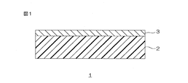
図1において、紙面上下方向は、上下方向(厚み方向、第1方向)であって、紙面上側が、上側(厚み方向一方側、第1方向一方側)、紙面下側が、下側(厚み方向他方側、第1方向他方側)である。図1において、紙面左右方向は、左右方向(幅方向、第1方向に直交する第2方向)であり、紙面左側が左側(第2方向一方側)、紙面右側が右側(第2方向他方側)である。図1において、紙厚方向は、前後方向(第1方向および第2方向に直交する第3方向)であり、紙面手前側が前側(第3方向一方側)、紙面奥側が後側(第3方向他方側)である。具体的には、各図の方向矢印に準拠する。
In FIG. 1, the vertical direction of the paper is the vertical direction (thickness direction, first direction), the upper side of the paper is the upper side (one side in the thickness direction, the first direction), and the lower side of the paper is the lower side (thickness direction). The other side, the other side in the first direction). In FIG. 1, the left-right direction on the paper surface is the left-right direction (width direction, second direction orthogonal to the first direction), the left side on the paper surface is the left side (second side in the second direction), and the right side on the paper surface is the right side (the other side in the second direction). ). In FIG. 1, the paper thickness direction is the front-rear direction (a third direction orthogonal to the first direction and the second direction), the front side of the paper is the front side (the third direction one side), and the back side of the paper surface is the rear side (the third direction). The other side). Specifically, it conforms to the direction arrow in each figure.
1.光透過性導電フィルム
光透過性導電フィルム1の一実施形態は、図1に示すように、所定の厚みを有するフィルム形状(シート形状を含む)をなし、厚み方向と直交する所定方向(前後方向および左右方向、すなわち、面方向)に延び、平坦な上面および平坦な下面(2つの主面)を有する。光透過性導電フィルム1は、例えば、調光フィルム4(後述、図2参照)などの一部品であり、つまり、調光装置(後述)ではない。すなわち、光透過性導電フィルム1は、調光フィルム4などを作製するための部品であり、調光機能層5などを含まず、部品単独で流通し、産業上利用可能なデバイスである。 1. As shown in FIG. 1, one embodiment of the light transmissiveconductive film 1 has a film shape (including a sheet shape) having a predetermined thickness, and a predetermined direction (front-rear direction) perpendicular to the thickness direction. And it extends in the left-right direction, that is, the surface direction, and has a flat upper surface and a flat lower surface (two main surfaces). The light transmissive conductive film 1 is, for example, one component such as a light control film 4 (see FIG. 2 described later), that is, not a light control device (described later). That is, the light-transmitting conductive film 1 is a component for producing the light control film 4 and the like, does not include the light control function layer 5 and the like, and is a device that can be distributed and used industrially.
光透過性導電フィルム1の一実施形態は、図1に示すように、所定の厚みを有するフィルム形状(シート形状を含む)をなし、厚み方向と直交する所定方向(前後方向および左右方向、すなわち、面方向)に延び、平坦な上面および平坦な下面(2つの主面)を有する。光透過性導電フィルム1は、例えば、調光フィルム4(後述、図2参照)などの一部品であり、つまり、調光装置(後述)ではない。すなわち、光透過性導電フィルム1は、調光フィルム4などを作製するための部品であり、調光機能層5などを含まず、部品単独で流通し、産業上利用可能なデバイスである。 1. As shown in FIG. 1, one embodiment of the light transmissive
具体的には、光透過性導電フィルム1は、光透過性基材2と、非晶質光透過性導電層3とを順に備える。つまり、光透過性導電フィルム1は、光透過性基材2と、光透過性基材2の上側に配置される非晶質光透過性導電層3とを備える。好ましくは、光透過性導電フィルム1は、光透過性基材2と、非晶質光透過性導電層3とのみからなる。以下、各層について詳述する。
Specifically, the light transmissive conductive film 1 includes a light transmissive substrate 2 and an amorphous light transmissive conductive layer 3 in this order. That is, the light transmissive conductive film 1 includes a light transmissive substrate 2 and an amorphous light transmissive conductive layer 3 disposed on the upper side of the light transmissive substrate 2. Preferably, the light transmissive conductive film 1 includes only the light transmissive substrate 2 and the amorphous light transmissive conductive layer 3. Hereinafter, each layer will be described in detail.
2.光透過性基材
光透過性基材2は、光透過性導電フィルム1の最下層であって、光透過性導電フィルム1の機械強度を確保する支持材である。 2. Light transmissive substrate The lighttransmissive substrate 2 is the lowermost layer of the light transmissive conductive film 1 and is a support material that ensures the mechanical strength of the light transmissive conductive film 1.
光透過性基材2は、光透過性導電フィルム1の最下層であって、光透過性導電フィルム1の機械強度を確保する支持材である。 2. Light transmissive substrate The light
光透過性基材2は、フィルム形状(シート形状を含む)を有している。
The light transmissive substrate 2 has a film shape (including a sheet shape).
光透過性基材2は、例えば、有機フィルム、例えば、ガラス板などの無機板からなる。光透過性基材2は、好ましくは、有機フィルム、より好ましくは、高分子フィルムからなる。有機フィルムは、水や有機ガスを含有しているため、非晶質光透過性導電層3の加熱による結晶化を抑制し、非晶質性をより一層維持することができる。
The light transmissive substrate 2 is made of, for example, an organic film, for example, an inorganic plate such as a glass plate. The light transmissive substrate 2 is preferably made of an organic film, more preferably a polymer film. Since the organic film contains water and organic gas, crystallization due to heating of the amorphous light-transmitting conductive layer 3 can be suppressed, and amorphousness can be further maintained.
高分子フィルムは、光透過性を有する。高分子フィルムの材料としては、例えば、ポリエチレンテレフタレート(PET)、ポリブチレンテレフタレート、ポリエチレンナフタレートなどのポリエステル樹脂、例えば、ポリメタクリレートなどの(メタ)アクリル樹脂(アクリル樹脂および/またはメタクリル樹脂)、例えば、ポリエチレン、ポリプロピレン、シクロオレフィンポリマーなどのオレフィン樹脂、例えば、ポリカーボネート樹脂、ポリエーテルスルフォン樹脂、ポリアリレート樹脂、メラミン樹脂、ポリアミド樹脂、ポリイミド樹脂、セルロース樹脂、ポリスチレン樹脂、ノルボルネン樹脂などが挙げられる。これら高分子フィルムは、単独使用または2種以上併用することができる。光透過性、耐熱性、機械特性などの観点から、好ましくは、ポリエステル樹脂が挙げられ、より好ましくは、PETが挙げられる。
The polymer film is light transmissive. Examples of the material of the polymer film include polyester resins such as polyethylene terephthalate (PET), polybutylene terephthalate, and polyethylene naphthalate, for example, (meth) acrylic resins (acrylic resin and / or methacrylic resin) such as polymethacrylate, And olefin resins such as polyethylene, polypropylene, and cycloolefin polymers such as polycarbonate resin, polyether sulfone resin, polyarylate resin, melamine resin, polyamide resin, polyimide resin, cellulose resin, polystyrene resin, norbornene resin, and the like. These polymer films can be used alone or in combination of two or more. From the viewpoints of light transmittance, heat resistance, mechanical properties, and the like, preferably, a polyester resin is used, and more preferably, PET is used.
光透過性基材2の厚みは、例えば、2μm以上、好ましくは、20μm以上、より好ましくは、40μm以上であり、また、例えば、300μm以下、好ましくは、200μm以下である。
The thickness of the light-transmitting substrate 2 is, for example, 2 μm or more, preferably 20 μm or more, more preferably 40 μm or more, and for example, 300 μm or less, preferably 200 μm or less.
光透過性基材2の厚みは、例えば、膜厚計を用いて測定することができる。
The thickness of the light transmissive substrate 2 can be measured using, for example, a film thickness meter.
光透過性基材2の下面には、セパレータなどを備えていてもよい。
A separator or the like may be provided on the lower surface of the light transmissive substrate 2.
3.非晶質光透過性導電層
非晶質光透過性導電層3は、非晶質の光透過性導電層であって、必要により後の工程でエッチングによりパターニングすることができる導電層である。 3. Amorphous light transmissive conductive layer The amorphous light transmissiveconductive layer 3 is an amorphous light transmissive conductive layer, and can be patterned by etching in a later step if necessary.
非晶質光透過性導電層3は、非晶質の光透過性導電層であって、必要により後の工程でエッチングによりパターニングすることができる導電層である。 3. Amorphous light transmissive conductive layer The amorphous light transmissive
非晶質光透過性導電層3は、フィルム形状(シート形状を含む)を有しており、光透過性基材2の上面全面に、光透過性基材2の上面に接触するように、配置されている。
The amorphous light transmissive conductive layer 3 has a film shape (including a sheet shape) and is in contact with the upper surface of the light transmissive substrate 2 on the entire upper surface of the light transmissive substrate 2. Has been placed.
非晶質光透過性導電層3の材料としては、例えば、In、Sn、Zn、Ga、Sb、Ti、Si、Zr、Mg、Al、Au、Ag、Cu、Pd、Wからなる群より選択される少なくとも1種の金属を含む金属酸化物が挙げられる。金属酸化物には、必要に応じて、さらに上記群に示された金属原子をドープしていてもよい。
The material of the amorphous light transmissive conductive layer 3 is selected from the group consisting of In, Sn, Zn, Ga, Sb, Ti, Si, Zr, Mg, Al, Au, Ag, Cu, Pd, and W, for example. And metal oxides containing at least one metal. If necessary, the metal oxide may be further doped with a metal atom shown in the above group.
非晶質光透過性導電層3としては、例えば、インジウムスズ複合酸化物(ITO)などのインジウム系導電性酸化物、例えば、アンチモンスズ複合酸化物(ATO)などのアンチモン系導電性酸化物などが挙げられる。非晶質光透過性導電層3は、表面抵抗を低下させる観点、および、優れた光透過性を確保する観点から、インジウム系導電性酸化物を含有し、より好ましくは、インジウムスズ複合酸化物(ITO)を含有する。すなわち、非晶質光透過性導電層3は、好ましくは、インジウム系導電性酸化物層であり、より好ましくは、ITO層である。これにより、低抵抗、光透過性に優れる。
Examples of the amorphous light-transmitting conductive layer 3 include indium-based conductive oxides such as indium tin composite oxide (ITO), and antimony-based conductive oxides such as antimony tin composite oxide (ATO). Is mentioned. The amorphous light-transmitting conductive layer 3 contains an indium-based conductive oxide, more preferably an indium tin composite oxide, from the viewpoint of reducing the surface resistance and ensuring excellent light transmittance. (ITO) is contained. That is, the amorphous light transmissive conductive layer 3 is preferably an indium conductive oxide layer, and more preferably an ITO layer. Thereby, it is excellent in low resistance and light transmittance.
非晶質光透過性導電層3の材料としてITOを用いる場合、酸化スズ(SnO2)含有量は、酸化スズおよび酸化インジウム(In2O3)の合計量に対して、例えば、0.5質量%以上、好ましくは、3質量%以上、より好ましくは、8質量%以上であり、また、例えば、25質量%以下、好ましくは、15質量%以下、より好ましくは、13質量%以下である。酸化スズの含有量を上記下限以上とすることにより、非晶質光透過性導電層3の低表面抵抗値(例えば、150Ω/□以下)を実現しつつ、結晶質への転化をより確実に抑制できる。また、酸化スズの含有量を上記上限以下とすることにより、光透過性や表面抵抗の安定性を向上させることができる。
When ITO is used as the material of the amorphous light transmissive conductive layer 3, the content of tin oxide (SnO 2 ) is, for example, 0.5% with respect to the total amount of tin oxide and indium oxide (In 2 O 3 ). % By mass or more, preferably 3% by mass or more, more preferably 8% by mass or more, and for example, 25% by mass or less, preferably 15% by mass or less, more preferably 13% by mass or less. . By making the content of tin oxide equal to or higher than the above lower limit, the conversion to crystalline is more reliably achieved while realizing the low surface resistance value (for example, 150Ω / □ or less) of the amorphous light-transmissive conductive layer 3. Can be suppressed. Moreover, the stability of light transmittance and surface resistance can be improved by making content of a tin oxide below the said upper limit.
本明細書中における「ITO」とは、少なくともインジウム(In)とスズ(Sn)とを含む複合酸化物であればよく、これら以外の追加成分を含んでもよい。追加成分としては、例えば、In、Sn以外の金属元素が挙げられ、具体的には、Zn、Ga、Sb、Ti、Si、Zr、Mg、Al、Au、Ag、Cu、Pd、W、Fe、Pb、Ni、Nb、Cr、Gaなどが挙げられる。
“ITO” in this specification may be a composite oxide containing at least indium (In) and tin (Sn), and may contain additional components other than these. Examples of the additional component include metal elements other than In and Sn. Specifically, Zn, Ga, Sb, Ti, Si, Zr, Mg, Al, Au, Ag, Cu, Pd, W, Fe , Pb, Ni, Nb, Cr, Ga and the like.
非晶質光透過性導電層3は、非晶質(アモルファス)の光透過性導電層であり、好ましくは、非晶質ITO層である。これにより、耐クラック性、耐擦傷性に優れる。
The amorphous light transmissive conductive layer 3 is an amorphous light transmissive conductive layer, and is preferably an amorphous ITO layer. Thereby, it is excellent in crack resistance and scratch resistance.
非晶質光透過性導電層3が非晶質であることは、例えば、非晶質光透過性導電層3がITO層である場合は、20℃の塩酸(濃度5質量%)に15分間浸漬した後、水洗・乾燥し、15mm程度の間の端子間抵抗を測定することで判断できる。本明細書においては、光透過性導電フィルム1を塩酸(20℃、濃度:5質量%)に浸漬・水洗・乾燥した後に、光透過性導電層における15mm間の端子間抵抗が10kΩ以上である場合、光透過性導電層が非晶質であるものとする。
The amorphous light-transmitting conductive layer 3 is amorphous. For example, when the amorphous light-transmitting conductive layer 3 is an ITO layer, it is placed in hydrochloric acid (concentration 5 mass%) at 20 ° C. for 15 minutes. After soaking, it can be judged by washing and drying, and measuring the resistance between terminals of about 15 mm. In the present specification, after the light-transmitting conductive film 1 is immersed, washed and dried in hydrochloric acid (20 ° C., concentration: 5 mass%), the resistance between terminals in the light-transmitting conductive layer is 15 kΩ or more. In this case, the light transmissive conductive layer is assumed to be amorphous.
非晶質光透過性導電層3は、好ましくは、不純物元素を含んでいる。不純物元素としては、非晶質光透過性導電層3を形成する際に使用するスパッタガス由来の元素(例えば、Ar元素)、光透過性基材2に含有される水や有機ガス由来の元素(例えば、H元素、C元素)が挙げられる。これらを含有することにより、非晶質光透過性導電層3の非晶質性をより一層向上させることができる。
The amorphous light transmissive conductive layer 3 preferably contains an impurity element. As the impurity element, an element derived from a sputtering gas (for example, Ar element) used when forming the amorphous light transmissive conductive layer 3, an element derived from water or organic gas contained in the light transmissive substrate 2. (For example, H element, C element). By containing these, the amorphous property of the amorphous light-transmitting conductive layer 3 can be further improved.
具体的には、非晶質光透過性導電層3に含有されるAr元素の含有量は、例えば、0.2atomic%以上、好ましくは、0.3atomic%以上であり、また、例えば、0.5atomic%以下、好ましくは、0.4atomic%以下である。Ar元素量を上記下限以上とすることにより、非晶質光透過性導電層3の非晶質性をより一層維持し易くできる。一方、Ar元素量を上記上限以下とすることにより、非晶質光透過性導電層3の抵抗変化率をより一層安定することができる。なお、Ar元素などの不純物元素の含有量は、スパッタリングの条件、例えば、スパッタ電源、磁場強度、気圧などを調整することにより、好適に調整することができる。
Specifically, the content of Ar element contained in the amorphous light transmissive conductive layer 3 is, for example, 0.2 atomic% or more, preferably 0.3 atomic% or more. It is 5 atomic% or less, preferably 0.4 atomic% or less. By setting the amount of Ar element to the above lower limit or more, the amorphous property of the amorphous light-transmitting conductive layer 3 can be more easily maintained. On the other hand, by making the amount of Ar element below the above upper limit, the resistance change rate of the amorphous light-transmitting conductive layer 3 can be further stabilized. Note that the content of an impurity element such as an Ar element can be suitably adjusted by adjusting sputtering conditions such as a sputtering power source, magnetic field strength, and atmospheric pressure.
非晶質光透過性導電層3の厚みは、例えば、10nm以上、好ましくは、30nm以上、より好ましくは、50nm以上であり、また、例えば、200nm以下、好ましくは、150nm以下、より好ましくは、100nm以下である。
The thickness of the amorphous light transmissive conductive layer 3 is, for example, 10 nm or more, preferably 30 nm or more, more preferably 50 nm or more, for example, 200 nm or less, preferably 150 nm or less, more preferably, 100 nm or less.
非晶質光透過性導電層3の厚みは、例えば、透過型電子顕微鏡を用いた断面観察により測定することができる。
The thickness of the amorphous light transmissive conductive layer 3 can be measured by, for example, cross-sectional observation using a transmission electron microscope. *
4.光透過性導電フィルムの製造方法
次に、光透過性導電フィルム1を製造する方法について説明する。 4). Next, a method for producing the light transmissiveconductive film 1 will be described.
次に、光透過性導電フィルム1を製造する方法について説明する。 4). Next, a method for producing the light transmissive
光透過性導電フィルム1は、光透過性基材2を用意し、非晶質光透過性導電層3を光透過性基材2の表面に形成することにより得られる。
The light transmissive conductive film 1 is obtained by preparing a light transmissive substrate 2 and forming an amorphous light transmissive conductive layer 3 on the surface of the light transmissive substrate 2.
例えば、非晶質光透過性導電層3を光透過性基材2の上面に、乾式により、配置(積層)する。
For example, the amorphous light transmissive conductive layer 3 is disposed (laminated) on the upper surface of the light transmissive substrate 2 by a dry method.
乾式としては、例えば、真空蒸着法、スパッタリング法、イオンプレーティング法などが挙げられる。好ましくは、スパッタリング法が挙げられる。
Examples of the dry method include a vacuum deposition method, a sputtering method, and an ion plating method. Preferably, a sputtering method is used.
スパッタリング法は、真空装置のチャンバー内にターゲットおよび被着体(光透過性基材2)を対向配置し、ガスを供給するとともに電圧を印加することによりガスイオンを加速しターゲットに照射させて、ターゲット表面からターゲット材料をはじき出して、そのターゲット材料を被着体表面に積層させる。
In the sputtering method, a target and an adherend (light-transmitting base material 2) are arranged opposite to each other in a chamber of a vacuum apparatus, and gas ions are accelerated by applying a voltage while supplying a gas to irradiate the target. The target material is ejected from the target surface, and the target material is laminated on the adherend surface.
スパッタリング法としては、例えば、2極スパッタリング法、ECR(電子サイクロトロン共鳴)スパッタリング法、マグネトロンスパッタリング法、イオンビームスパッタリング法などが挙げられる。好ましくは、マグネトロンスパッタリング法が挙げられる。
Examples of the sputtering method include a bipolar sputtering method, an ECR (electron cyclotron resonance) sputtering method, a magnetron sputtering method, and an ion beam sputtering method. A magnetron sputtering method is preferable.
スパッタリング法に用いる電源は、例えば、直流(DC)電源、交流中周波(AC/MF)電源、高周波(RF)電源、直流電源を重畳した高周波電源のいずれであってもよい。
The power source used for the sputtering method may be, for example, a direct current (DC) power source, an alternating current medium frequency (AC / MF) power source, a high frequency (RF) power source, or a high frequency power source on which a direct current power source is superimposed.
ターゲットとしては、非晶質光透過性導電層3を構成する上述の金属酸化物が挙げられる。例えば、非晶質光透過性導電層3の材料としてITOを用いる場合、ITOからなるターゲットを用いる。ターゲットにおける酸化スズ(SnO2)含有量は、酸化スズおよび酸化インジウム(In2O3)の合計量に対して、例えば、0.5質量%以上、好ましくは、3質量%以上、より好ましくは、8質量%以上であり、また、例えば、25質量%以下、好ましくは、15質量%以下、より好ましくは、13質量%以下である。
Examples of the target include the above-described metal oxides constituting the amorphous light-transmitting conductive layer 3. For example, when ITO is used as the material of the amorphous light transmissive conductive layer 3, a target made of ITO is used. The tin oxide (SnO 2 ) content in the target is, for example, 0.5% by mass or more, preferably 3% by mass or more, more preferably, with respect to the total amount of tin oxide and indium oxide (In 2 O 3 ). 8% by mass or more, and for example, 25% by mass or less, preferably 15% by mass or less, and more preferably 13% by mass or less.
ターゲット表面の水平磁場の強度は、成膜速度、非晶質光透過性導電層3に対する不純物の取り込みなどの観点から、例えば、10mT以上200mT以下である。
The strength of the horizontal magnetic field on the target surface is, for example, 10 mT or more and 200 mT or less from the viewpoints of film formation speed, impurity incorporation into the amorphous light-transmitting conductive layer 3, and the like.
スパッタリング時の放電気圧は、例えば、1.0Pa以下、好ましくは、0.5Pa以下であり、また、例えば、0.01Pa以上である。
The discharge pressure during sputtering is, for example, 1.0 Pa or less, preferably 0.5 Pa or less, and for example, 0.01 Pa or more.
スパッタリング時の光透過性基材2の温度は、非晶質光透過性導電層3の非晶質性を維持する観点から、例えば、180℃以下であり、好ましくは、90℃以下である。光透過性基材2の温度が上記範囲を超えると、非晶質光透過性導電層3が得られず、スパッタリングと同時に結晶質に転化するおそれがある。
The temperature of the light-transmitting substrate 2 during sputtering is, for example, 180 ° C. or less, preferably 90 ° C. or less, from the viewpoint of maintaining the amorphous property of the amorphous light-transmitting conductive layer 3. If the temperature of the light-transmitting substrate 2 exceeds the above range, the amorphous light-transmitting conductive layer 3 cannot be obtained, and there is a possibility that it will be converted to crystalline simultaneously with sputtering.
スパッタリング法で用いられるガスとしては、例えば、Arなどの不活性ガスが挙げられる。また、この方法では、酸素ガスなどの反応性ガスを併用する。反応性ガスの流量の、不活性ガスの流量に対する比(反応性ガスの流量(sccm)/不活性ガスの流量(sccm))は、例えば、0.1/100以上5/100以下である。
Examples of the gas used in the sputtering method include an inert gas such as Ar. In this method, a reactive gas such as oxygen gas is used in combination. The ratio of the flow rate of the reactive gas to the flow rate of the inert gas (reactive gas flow rate (sccm) / inert gas flow rate (sccm)) is, for example, 0.1 / 100 or more and 5/100 or less.
この方法では、特に、酸素ガス量を調整することにより、後述する特性の光透過性導電フィルム1を得ることができる。
In this method, in particular, the light-transmitting conductive film 1 having the characteristics described later can be obtained by adjusting the amount of oxygen gas.
すなわち、例えば、スパッタリング法により、非晶質光透過性導電層3としてITO層を形成する場合を例に挙げると、スパッタリング法により得られるITO層は、一般的に、非晶質のITO層として成膜される。このとき、非晶質ITO層内部に導入される酸素導入量により、非晶質ITO層の膜質が変化する。具体的には、非晶質ITO層内部に導入される酸素導入量が、適量よりも少ない場合(酸素不足状態)では、大気雰囲気下での加熱により結晶質へと転化し、その結果、加熱後の表面抵抗値が大きく低減する。一方、非晶質ITO層に含有される酸素導入量が、適量であると、大気雰囲気下での加熱を経た場合であっても非晶質構造を維持し、抵抗変化率は小さい。他方、非晶質ITOに含有される酸素導入量が適量より過剰であると、大気雰囲気下での加熱により非晶質構造を維持するが、加熱後の表面抵抗値が大きく増大し、抵抗変化率が大きい。
That is, for example, when an ITO layer is formed as the amorphous light transmissive conductive layer 3 by sputtering, for example, the ITO layer obtained by sputtering is generally an amorphous ITO layer. A film is formed. At this time, the film quality of the amorphous ITO layer changes depending on the amount of oxygen introduced into the amorphous ITO layer. Specifically, when the amount of oxygen introduced into the amorphous ITO layer is less than an appropriate amount (oxygen-deficient state), it is converted to crystalline by heating in an air atmosphere, and as a result The subsequent surface resistance value is greatly reduced. On the other hand, when the amount of oxygen introduced in the amorphous ITO layer is an appropriate amount, the amorphous structure is maintained even when the heating is performed in an air atmosphere, and the resistance change rate is small. On the other hand, if the amount of oxygen introduced in the amorphous ITO is more than the appropriate amount, the amorphous structure is maintained by heating in the air atmosphere, but the surface resistance value after heating increases greatly, and the resistance change The rate is large.
上記の理由は、以下のように推察される。なお、本発明は、以下の理論に限定されるものではない。非晶質ITO層に含まれる酸素量が少ない場合(酸素不足状態)では、非晶質ITO層は、その構造において多数の酸素欠損部を有しているため、ITO膜を構成する各原子が熱振動により動きやすく、最適構造をとりやすい。そのため、大気雰囲気下での加熱により、酸素を酸素欠損部に適度に取り込みながら、最適構造(結晶質構造)を取り、その結果、表面抵抗値が大きく低減する。一方、非晶質ITOに含有される酸素導入量が、適量範囲であると、非晶質ITO層に酸素欠損部が生じにくい。即ち、酸素の適量範囲とは、非晶質ITOが化学量論組成をとりやすい範囲を示す。酸素量が適量であると、非晶質ITOは大気雰囲気下で加熱した場合であっても、酸素欠損部が少ない為、過度に酸化することなく、良質な非晶質構造を維持する。他方、非晶質ITOに含有される酸素導入量が過剰である場合、非晶質ITO膜内に含まれる酸素原子は不純物として作用する。不純物原子は、好適な含有水準を超えると中性子散乱の要因となり、表面抵抗値を増大させる。そのため、非晶質ITOに含有される酸素導入量が過剰であると、加熱によりITO内の酸素量が更に過剰となり、表面抵抗値が大きく増大すると推察される。
The above reasons are presumed as follows. Note that the present invention is not limited to the following theory. When the amount of oxygen contained in the amorphous ITO layer is small (oxygen-deficient state), the amorphous ITO layer has a large number of oxygen vacancies in its structure. Easy to move due to thermal vibration and easy to take optimum structure. For this reason, an optimum structure (crystalline structure) is taken while appropriately taking oxygen into the oxygen deficient part by heating in an air atmosphere, and as a result, the surface resistance value is greatly reduced. On the other hand, when the amount of oxygen introduced in the amorphous ITO is within an appropriate range, oxygen deficient portions are unlikely to occur in the amorphous ITO layer. That is, the appropriate amount range of oxygen indicates a range in which amorphous ITO easily takes a stoichiometric composition. When the amount of oxygen is appropriate, amorphous ITO maintains a good quality amorphous structure without excessive oxidation because it has few oxygen deficient portions even when heated in an air atmosphere. On the other hand, when the amount of oxygen introduced in the amorphous ITO is excessive, oxygen atoms contained in the amorphous ITO film act as impurities. Impurity atoms cause neutron scattering when they exceed a suitable content level, and increase the surface resistance value. Therefore, if the amount of oxygen introduced into amorphous ITO is excessive, it is presumed that the amount of oxygen in ITO further increases due to heating, and the surface resistance value increases greatly.
具体的には、例えば、ITO内に含有される酸素量が適量範囲となるように、チャンバーに供給する酸素ガスの供給割合を調整する。
Specifically, for example, the supply ratio of oxygen gas supplied to the chamber is adjusted so that the amount of oxygen contained in the ITO falls within an appropriate range.
酸素ガスの供給割合の好適値は、真空装置のスパッタリング電源や磁場強度、チャンバー容積などの設備的要因、光透過性基材2に微小に含有される反応性ガス量(水など)などの材料的要因に応じて、適宜設定される。例えば、反応性ガスを含有する高分子フィルムと、反応性ガスを含有しないガラス基材とでは、酸素ガス供給量を低減できるため、高分子フィルムが好ましい。また、磁場強度および電源はO2プラズマの生成量に関係するため、採用する磁場強度、電源により酸素ガス供給量は変化するが、光透過性基材2にかかる熱量を低減し非晶質性を高める観点から、低磁場であることが好ましく、また、成膜レートの観点から、直流電源が好ましい。
Suitable values for the oxygen gas supply ratio include materials such as sputtering equipment power source, magnetic field strength, chamber volume, and the like, and the amount of reactive gas (such as water) contained in the light-transmitting substrate 2 minutely. It is set as appropriate according to the specific factors. For example, a polymer film containing a reactive gas and a glass substrate not containing a reactive gas can reduce the oxygen gas supply amount, and therefore a polymer film is preferable. In addition, since the magnetic field strength and the power source are related to the amount of O 2 plasma generated, the amount of oxygen gas supplied varies depending on the magnetic field strength and the power source employed, but the amount of heat applied to the light-transmitting substrate 2 is reduced and amorphous. From the viewpoint of enhancing the film thickness, a low magnetic field is preferable, and from the viewpoint of the film formation rate, a direct current power source is preferable.
具体的には、例えば、光透過性基材2として高分子フィルムを用い、水平磁場強度を1~50mT(好ましくは、20~40mT)の低磁場強度とし、直流電源を採用した場合、Arガスに対する酸素ガスの割合(O2/Ar)は、例えば、0.022以上、好ましくは、0.025以上、より好ましくは、0.028以上であり、また、例えば、0.036以下、好ましくは、0.035以下、より好ましくは、0.034以下である。
Specifically, for example, when a polymer film is used as the light-transmitting substrate 2, the horizontal magnetic field strength is set to a low magnetic field strength of 1 to 50 mT (preferably 20 to 40 mT), and a DC power source is employed, Ar gas is used. The ratio of oxygen gas to (O 2 / Ar) is, for example, 0.022 or more, preferably 0.025 or more, more preferably 0.028 or more, and for example, 0.036 or less, preferably 0.035 or less, and more preferably 0.034 or less.
また、例えば、光透過性基材2として高分子フィルムを用い、水平磁場強度を50~200mT(好ましくは、80~120mT)の高磁場強度とし、直流電源を採用した場合、Arガスに対する酸素ガスの割合(O2/Ar)は、例えば、0.018以上、好ましくは、0.020以上、より好ましくは、0.022以上であり、また、例えば、0.035以下、好ましくは、0.034以下、より好ましくは、0.033以下、さらに好ましくは、0.025以下である。
In addition, for example, when a polymer film is used as the light-transmitting substrate 2, the horizontal magnetic field strength is set to a high magnetic field strength of 50 to 200 mT (preferably 80 to 120 mT), and a DC power source is employed, oxygen gas relative to Ar gas The ratio (O 2 / Ar) is, for example, 0.018 or more, preferably 0.020 or more, more preferably 0.022 or more, and for example, 0.035 or less, preferably 0. 034 or less, more preferably 0.033 or less, and still more preferably 0.025 or less.
なお、ITOに酸素が適した割合で導入されているか否かは、例えば、スパッタリングにおいて供給される酸素供給量(sccm)(X軸)と、その酸素供給量によって得られるITOの表面抵抗値(Ω/□)(Y軸)とをグラフにプロットしてそのグラフにより判断することができる。すなわち、そのグラフの極小近傍領域が、最も表面抵抗値が小さく、ITOが化学量論組成となっているため、その極小近傍領域のX軸の値が、ITOに化学量論組成の酸素を導入させている適した酸素供給量と判断できる。
Note that whether or not oxygen is introduced into the ITO at an appropriate ratio depends on, for example, the oxygen supply amount (sccm) (X-axis) supplied in sputtering and the surface resistance value of ITO obtained by the oxygen supply amount ( Ω / □) (Y-axis) can be plotted on a graph and judged from the graph. That is, the region near the minimum in the graph has the smallest surface resistance value, and ITO has a stoichiometric composition. Therefore, the X-axis value in the region near the minimum introduces oxygen having a stoichiometric composition into the ITO. It can be determined that the oxygen supply is suitable.
これによって、光透過性基材2と、非晶質光透過性導電層3とを備える光透過性導電フィルム1(加熱処理前)を得る。
Thereby, a light transmissive conductive film 1 (before heat treatment) including the light transmissive substrate 2 and the amorphous light transmissive conductive layer 3 is obtained.
光透過性導電フィルム1の総厚みは、例えば、2μm以上、好ましくは、20μm以上であり、また、例えば、300μm以下、好ましくは、200μm以下である。
The total thickness of the light-transmissive conductive film 1 is, for example, 2 μm or more, preferably 20 μm or more, and for example, 300 μm or less, preferably 200 μm or less.
このようにして得られる光透過性導電フィルム1は、以下の特性を備える。
The light transmissive conductive film 1 thus obtained has the following characteristics.
非晶質光透過性導電層3における、加熱処理前のキャリア密度(Xa×1019/cm3)は、例えば、10.0×1019/cm3以上、好ましくは、20.0×1019/cm3以上、より好ましくは、29.0×1019/cm3以上であり、また、例えば、50.0×1019/cm3以下、好ましくは、43.0×1019/cm3以下である。
The carrier density (Xa × 10 19 / cm 3 ) before the heat treatment in the amorphous light-transmissive conductive layer 3 is, for example, 10.0 × 10 19 / cm 3 or more, preferably 20.0 × 10 19. / Cm 3 or more, more preferably 29.0 × 10 19 / cm 3 or more, for example, 50.0 × 10 19 / cm 3 or less, preferably 43.0 × 10 19 / cm 3 or less. It is.
非晶質光透過性導電層3における、加熱処理前のホール移動度(Ya cm2/V・s)は、例えば、10.0cm2/V・s以上、好ましくは、15.0cm2/V・s以上、より好ましくは、28.0cm2/V・s以上であり、また、例えば、50.0cm2/V・s以下、好ましくは、36.5cm2/V・s以下である。
The hole mobility (Ya cm 2 / V · s) before the heat treatment in the amorphous light-transmissive conductive layer 3 is, for example, 10.0 cm 2 / V · s or more, preferably 15.0 cm 2 / V. · s or more, and more preferably not 28.0cm 2 / V · s or more, and is, for example, 50.0 cm 2 / V · s or less, or preferably less 36.5cm 2 / V · s.
非晶質光透過性導電層3における、加熱処理前の表面抵抗値は、例えば、1Ω/□以上、好ましくは、10Ω/□以上であり、また、例えば、200Ω/□以下、好ましくは、150Ω/□以下、より好ましくは、100Ω/□未満である。
The surface resistance value before the heat treatment in the amorphous light-transmissive conductive layer 3 is, for example, 1Ω / □ or more, preferably 10Ω / □ or more, and for example, 200Ω / □ or less, preferably 150Ω. / □ or less, more preferably less than 100Ω / □.
なお、加熱処理前とは、例えば、光透過性導電フィルム1を製造した後から、80℃以上に加熱する以前をいう。
Note that “before heat treatment” means, for example, after the light-transmitting conductive film 1 is manufactured and before being heated to 80 ° C. or higher.
非晶質光透過性導電層3を加熱処理した後の被加熱光透過性導電層のキャリア密度(Xc×1019/cm3)は、例えば、15.0×1019/cm3以上、好ましくは、20.0×1019/cm3以上、より好ましくは、30.0×1019/cm3以上であり、また、例えば、150.0×1019/cm3以下、好ましくは、100.0×1019/cm3以下、より好ましくは、80.0×1019/cm3以下である。
The carrier density (Xc × 10 19 / cm 3 ) of the heated light-transmitting conductive layer after heat-treating the amorphous light-transmitting conductive layer 3 is, for example, 15.0 × 10 19 / cm 3 or more, preferably Is 20.0 × 10 19 / cm 3 or more, more preferably 30.0 × 10 19 / cm 3 or more, for example, 150.0 × 10 19 / cm 3 or less, preferably 100. 0 × 10 19 / cm 3 or less, more preferably 80.0 × 10 19 / cm 3 or less.
被加熱光透過性導電層のホール移動度(Yc cm2/V・s)は、例えば、10.0cm2/V・s以上、好ましくは、15.0cm2/V・s以上であり、また、例えば、35.0cm2/V・s以下、好ましくは、30.0cm2/V・s以下、より好ましくは、23.5cm2/V・s以下、さらに好ましくは、22.5cm2/V・s以下である。
The hole mobility (Yc cm 2 / V · s) of the heated light-transmitting conductive layer is, for example, 10.0 cm 2 / V · s or more, preferably 15.0 cm 2 / V · s or more. , for example, 35.0cm 2 / V · s or less, preferably, 30.0cm 2 / V · s or less, more preferably, 23.5cm 2 / V · s or less, more preferably, 22.5cm 2 / V -S or less.
被加熱光透過性導電層の表面抵抗値は、例えば、1Ω/□以上、好ましくは、10Ω/□以上であり、また、例えば、200Ω/□以下、好ましくは、150Ω/□以下、より好ましくは、100Ω/□未満である。
The surface resistance value of the heated light-transmitting conductive layer is, for example, 1Ω / □ or more, preferably 10Ω / □ or more, and for example, 200Ω / □ or less, preferably 150Ω / □ or less, more preferably , Less than 100Ω / □.
被加熱光透過性導電層とは、非晶質光透過性導電層3を大気環境下で加熱処理した後の光透過性導電層を指す。この加熱処理の温度および暴露時間は、非晶質光透過性導電層3の長期信頼性を確認する観点で、例えば、80℃で500時間である。また、長期信頼性評価の加速試験として加熱処理を実施する場合は、例えば、140℃で1~2時間とすることもできる。
The heated light-transmitting conductive layer refers to a light-transmitting conductive layer after the amorphous light-transmitting conductive layer 3 is heat-treated in an atmospheric environment. The temperature of the heat treatment and the exposure time are, for example, 500 hours at 80 ° C. from the viewpoint of confirming long-term reliability of the amorphous light-transmitting conductive layer 3. Further, when heat treatment is performed as an accelerated test for long-term reliability evaluation, for example, it can be performed at 140 ° C. for 1 to 2 hours.
また、非晶質光透過性導電層3のキャリア密度(Xa×1019/cm3)と、被加熱光透過性導電層とのキャリア密度(Xc×1019/cm3)とでは、Xa≦Xcの式(1)を満たし、好ましくは、Xa<Xcの式(1´)を満たす。Xa>Xcの関係を満たすと、非晶質光透過性導電層3は、表面抵抗値が大きく増加するため、加熱時の安定性に劣る。
Further, when the carrier density (Xa × 10 19 / cm 3 ) of the amorphous light-transmitting conductive layer 3 and the carrier density (Xc × 10 19 / cm 3 ) of the heated light-transmitting conductive layer are Xa ≦ Xc expression (1) is satisfied, and preferably Xa <Xc expression (1 ′) is satisfied. If the relationship of Xa> Xc is satisfied, the amorphous light-transmitting conductive layer 3 has a greatly increased surface resistance value, and thus is inferior in stability during heating.
特に、加熱前後のキャリア密度の比、すなわち、Xaに対するXcの比(Xc/Xa)は、好ましくは、1.00を超過し、より好ましくは、1.05以上、さらに好ましくは、1.10以上である。また、好ましくは、2.00未満であり、より好ましくは、1.80以下である。上記比を上記範囲とすることにより、加熱による抵抗変化を確実に抑制し、熱安定性がより一層優れる。
In particular, the ratio of carrier density before and after heating, that is, the ratio of Xc to Xa (Xc / Xa) is preferably more than 1.00, more preferably 1.05 or more, and even more preferably 1.10. That's it. Moreover, Preferably it is less than 2.00, More preferably, it is 1.80 or less. By making the said ratio into the said range, the resistance change by heating is suppressed reliably and thermal stability is further excellent.
非晶質光透過性導電層3のホール移動度(Ya cm2/V・s)と、被加熱光透過性導電層とのホール移動度(Ya cm2/V・s)とでは、Ya≧Ycの式(2)を満たし、好ましくは、Ya>Ycの式(2´)を満たす。Ya<Ycの関係を満たすと、非晶質光透過性導電層3は、加熱処理により結晶化して表面抵抗値が大きく低下しやすく、その結果、加熱時の安定性に劣る。
Amorphous light transmissive conductive layer 3 of the hole mobility and (Ya cm 2 / V · s ), with a hole mobility of the heated light-transmitting conductive layer (Ya cm 2 / V · s ) is, Ya ≧ The expression (2) of Yc is satisfied, and preferably the expression (2 ′) of Ya> Yc is satisfied. When the relationship of Ya <Yc is satisfied, the amorphous light-transmitting conductive layer 3 is crystallized by the heat treatment, and the surface resistance value is likely to be greatly reduced, resulting in poor stability during heating.
特に、加熱前後のホール移動度の比、すなわち、Yaに対するYcの比(Yc/Ya)は、好ましくは、1.00未満であり、より好ましくは、0.75以下である。また、好ましくは、0.50を超過し、より好ましくは、0.60以上である。上記比を上記範囲とすることにより、加熱による抵抗変化を確実に抑制し、熱安定性がより一層優れる。
Particularly, the ratio of hole mobility before and after heating, that is, the ratio of Yc to Ya (Yc / Ya) is preferably less than 1.00, and more preferably 0.75 or less. Moreover, Preferably, it exceeds 0.50, More preferably, it is 0.60 or more. By making the said ratio into the said range, the resistance change by heating is suppressed reliably and thermal stability is further excellent.
移動距離Lを、{(Xc-Xa)2+(Yc-Ya)2}1/2としたときに(図3参照)、Lは、1.0以上45.0以下である。好ましくは、10.0以上、より好ましくは、13.0以上であり、また、好ましくは、40.0以下、より好ましくは、35.0未満、さらに好ましくは、33.0以下である。移動距離Lが上記範囲とすることにより、加熱前後の非晶質光透過性導電層3の膜質変化が小さく、特に熱安定性に優れる。
When the movement distance L is {(Xc−Xa) 2 + (Yc−Ya) 2 } 1/2 (see FIG. 3), L is 1.0 or more and 45.0 or less. Preferably, it is 10.0 or more, more preferably 13.0 or more, preferably 40.0 or less, more preferably less than 35.0, and still more preferably 33.0 or less. When the moving distance L is in the above range, the film quality change of the amorphous light-transmitting conductive layer 3 before and after heating is small, and particularly excellent in thermal stability.
また、加熱前後のキャリア密度の比(Xc/Xa)と、加熱前後のホール移動度の比(Yc/Ya)との積、すなわち、(Yc/Ya)×(Xc/Xa)は、例えば、0.50以上、好ましくは、0.65以上、さらに好ましくは、0.75以上であり、また、例えば、1.80以下、好ましくは、1.50以下、さらに好ましくは、1.30以下である。加熱前後のキャリア密度の比率およびホール移動度の比率を上記一定の範囲内とすることにより、結晶性を抑制することができ、また、抵抗変化を抑制することができる。
Further, the product of the ratio (Xc / Xa) of the carrier density before and after heating and the ratio (Yc / Ya) of the hole mobility before and after heating, that is, (Yc / Ya) × (Xc / Xa) is, for example, 0.50 or more, preferably 0.65 or more, more preferably 0.75 or more, and for example, 1.80 or less, preferably 1.50 or less, more preferably 1.30 or less. is there. By setting the ratio of the carrier density before and after heating and the ratio of the hole mobility within the above-mentioned fixed ranges, crystallinity can be suppressed and resistance change can be suppressed.
被加熱光透過性導電層は、好ましくは、非晶質である。これにより、熱安定性に優れるとともに、耐クラック性および耐擦傷性に優れる。
The heated light-transmitting conductive layer is preferably amorphous. Thereby, while being excellent in thermal stability, it is excellent in crack resistance and scratch resistance.
そして、この光透過性導電フィルム1は、光透過性基材2と、非晶質光透過性導電層3とを備えるため、耐クラック性、耐擦傷性などに優れる。
And since this light-transmitting conductive film 1 includes the light-transmitting substrate 2 and the amorphous light-transmitting conductive layer 3, it is excellent in crack resistance, scratch resistance, and the like.
また、加熱前の非晶質光透過性導電層3および被加熱光透過性導電層における、ホール移動度およびキャリア密度が、所定の条件を満たすため、熱による非晶質光透過性導電層3の抵抗率の変化が抑制することができ、熱安定性に優れる。
In addition, since the hole mobility and the carrier density in the amorphous light-transmitting conductive layer 3 and the heated light-transmitting conductive layer before heating satisfy predetermined conditions, the amorphous light-transmitting conductive layer 3 due to heat is used. The change in resistivity can be suppressed, and the thermal stability is excellent.
特に、本発明者らは、非晶質光透過性導電層3の比抵抗は、ホール移動度とキャリア密度との掛け算に反比例することから、加熱による抵抗変化を小さくするには、加熱前後でホール移動度の挙動とキャリア密度の挙動とが逆になるよう、非晶質光透過性導電層3の膜質を設計する必要があるという着想に至り、本発明に至った。つまり、本発明の非晶質光透過性導電層3が上記式(1)~(3)を満たす、すなわち、非晶質光透過性導電層3において、加熱処理後のホール移動度を小さくさせ、加熱後のキャリア密度を大きくさせ、移動距離Lを小さくさせるよう膜設計を実施することにより、加熱前後の比抵抗の値の変化を抑制させる。その結果、加熱による抵抗変化が少なく、熱安定性に優れる。
In particular, since the specific resistance of the amorphous light-transmitting conductive layer 3 is inversely proportional to the multiplication of the hole mobility and the carrier density, before and after heating, the resistance change due to heating can be reduced. The inventor came up with the idea that the film quality of the amorphous light-transmitting conductive layer 3 needs to be designed so that the behavior of hole mobility and the behavior of carrier density are reversed. That is, the amorphous light-transmitting conductive layer 3 of the present invention satisfies the above formulas (1) to (3), that is, in the amorphous light-transmitting conductive layer 3, the hole mobility after heat treatment is reduced. The film design is performed so as to increase the carrier density after heating and to decrease the moving distance L, thereby suppressing the change in the specific resistance value before and after heating. As a result, the resistance change due to heating is small and the thermal stability is excellent.
この光透過性導電フィルム1は、産業上利用可能なデバイスである。
The light transmissive conductive film 1 is an industrially available device.
なお、この光透過性導電フィルム1は、必要に応じてエッチングを実施して、非晶質光透過性導電層3を、所定形状にパターニングすることができる。
The light transmissive conductive film 1 can be etched as necessary to pattern the amorphous light transmissive conductive layer 3 into a predetermined shape.
また、上記した製造方法を、ロールトゥロール方式で実施、また、バッチ方式で実施することもできる。
Moreover, the above-described manufacturing method can be performed by a roll-to-roll method or a batch method.
5.調光フィルムの製造方法
次に、上記した光透過性導電フィルム1を用いて調光フィルム4を製造する方法について図2を参照して説明する。 5. 2. Manufacturing method of light control film Next, the method of manufacturing thelight control film 4 using the above-mentioned light transmissive conductive film 1 is demonstrated with reference to FIG.
次に、上記した光透過性導電フィルム1を用いて調光フィルム4を製造する方法について図2を参照して説明する。 5. 2. Manufacturing method of light control film Next, the method of manufacturing the
この方法は、図2に示すように、上記した光透過性導電フィルム1を2つ製造する工程と、次いで、調光機能層5を2つの光透過性導電フィルム1によって挟む工程とを備える。
As shown in FIG. 2, this method includes a step of manufacturing two light transmissive conductive films 1 and a step of sandwiching the light control function layer 5 between the two light transmissive conductive films 1.
まず、上記した光透過性導電フィルム1を2つ製造する。なお、1つの光透過性導電フィルム1を切断加工して、2つの光透過性導電フィルム1を用意することもできる。
First, two light transmissive conductive films 1 described above are manufactured. In addition, the two light transmissive conductive films 1 can also be prepared by cutting one light transmissive conductive film 1.
2つの光透過性導電フィルム1は、第1の光透過性導電フィルム1A、および、第2の光透過性導電フィルム1Bである。
The two light transmissive conductive films 1 are a first light transmissive conductive film 1A and a second light transmissive conductive film 1B.
次いで、調光機能層5を、第1の光透過性導電フィルム1Aにおける非晶質光透過性導電層3の上面(表面)に、例えば、湿式により、形成する。
Next, the light control function layer 5 is formed on the upper surface (surface) of the amorphous light transmissive conductive layer 3 in the first light transmissive conductive film 1A by, for example, wet processing.
例えば、液晶組成物を含む溶液を、第1の光透過性導電フィルム1Aにおける非晶質光透過性導電層3の上面に塗布する。液晶組成物は、溶液に含まれる公知のものが挙げられ、例えば、特開平8-194209号公報に記載の液晶分散樹脂が挙げられる。
For example, a solution containing a liquid crystal composition is applied to the upper surface of the amorphous light transmissive conductive layer 3 in the first light transmissive conductive film 1A. Examples of the liquid crystal composition include known ones contained in a solution, for example, a liquid crystal dispersion resin described in JP-A-8-194209.
続いて、第2の光透過性導電フィルム1Bを塗膜の表面に、第2の光透過性導電フィルム1Bの非晶質光透過性導電層3と塗膜とが接触するように、積層する。これによって、2つの光透過性導電フィルム1、つまり、第1の光透過性導電フィルム1Aおよび第2の光透過性導電フィルム1Bによって、塗膜を挟み込む。
Subsequently, the second light-transmissive conductive film 1B is laminated on the surface of the coating film so that the amorphous light-transmissive conductive layer 3 of the second light-transmissive conductive film 1B and the coating film are in contact with each other. . Thus, the coating film is sandwiched between the two light transmissive conductive films 1, that is, the first light transmissive conductive film 1A and the second light transmissive conductive film 1B.
その後、塗膜に対して適宜の処理(例えば、光硬化処理や熱乾燥処理など)を施して、調光機能層5を形成する。調光機能層5は、第1の光透過性導電フィルム1Aの非晶質光透過性導電層3と、第2の光透過性導電フィルム1Bの非晶質光透過性導電層3との間に形成される。
Thereafter, an appropriate treatment (for example, photocuring treatment or heat drying treatment) is performed on the coating film to form the light control function layer 5. The light control function layer 5 is provided between the amorphous light transmissive conductive layer 3 of the first light transmissive conductive film 1A and the amorphous light transmissive conductive layer 3 of the second light transmissive conductive film 1B. Formed.
これによって、第1の光透過性導電フィルム1Aと、調光機能層5と、第2の光透過性導電フィルム1Bとを順に備える調光フィルム4を得る。
Thereby, the light control film 4 provided with the 1st light transmissive conductive film 1A, the light control function layer 5, and the 2nd light transmissive conductive film 1B in order is obtained.
そして、調光フィルム4は、電源(図示せず)、制御装置(図示せず)などを備える調光装置(図示せず、例えば、調光窓など)に備えられる。図示しない調光装置では、電源によって、第1の光透過性導電フィルム1Aにおける非晶質光透過性導電層3と、第2の光透過性導電フィルム1Bにおける非晶質光透過性導電層3とに電圧が印加され、それによって、それらの間において電界が発生する。
And the light control film 4 is provided in the light control apparatus (not shown, for example, a light control window etc.) provided with a power supply (not shown), a control apparatus (not shown), etc. In a light control device (not shown), the amorphous light-transmitting conductive layer 3 in the first light-transmitting conductive film 1A and the amorphous light-transmitting conductive layer 3 in the second light-transmitting conductive film 1B are turned on by a power source. And a voltage is applied to them, thereby generating an electric field between them.
そして、制御装置に基づいて、上記した電界が制御されることによって、第1の光透過性導電フィルム1Aと第2の光透過性導電フィルム1Bとの間に位置する調光機能層5が、光を遮断し、または、透過させる。
And the light control function layer 5 located between the 1st light transmissive conductive film 1A and the 2nd light transmissive conductive film 1B by controlling the above-mentioned electric field based on a control device, Block or transmit light.
そして、この調光フィルム4は、光透過性導電フィルム1を備えているため、加工性や運搬性が良好である。また、表面抵抗のムラの発生、ひいては、調光機能層5の配向ムラの発生を長期間抑制できるため、調光のばらつきを低減することができる。
And since this light control film 4 is equipped with the translucent conductive film 1, workability and transportability are favorable. In addition, the occurrence of uneven surface resistance, and hence the occurrence of uneven alignment in the light control function layer 5, can be suppressed for a long period of time, so that variations in light control can be reduced.
6.変形例
図1の実施形態では、光透過性基材2の表面に非晶質光透過性導電層3が直接配置されているが、例えば、図示しないが、光透過性基材2の上面および/または下面に、機能層を設けることができる。 6). In the embodiment of FIG. 1, the amorphous light transmissiveconductive layer 3 is directly disposed on the surface of the light transmissive substrate 2. For example, although not illustrated, the upper surface of the light transmissive substrate 2 and A functional layer can be provided on the lower surface.
図1の実施形態では、光透過性基材2の表面に非晶質光透過性導電層3が直接配置されているが、例えば、図示しないが、光透過性基材2の上面および/または下面に、機能層を設けることができる。 6). In the embodiment of FIG. 1, the amorphous light transmissive
すなわち、例えば、光透過性導電フィルム1は、光透過性基材2と、光透過性基材2の上面に配置される機能層と、機能層の上面に配置される非晶質光透過性導電層3とを備えることができる。また、例えば、光透過性導電フィルム1は、光透過性基材2と、光透過性基材2の上面に配置される非晶質光透過性導電層3と、光透過性基材2の下面に配置される機能層とを備えることができる。また、例えば、光透過性基材2の上側および下側に、機能層と非晶質光透過性導電層3とをこの順に備えることもできる。
That is, for example, the light transmissive conductive film 1 includes a light transmissive substrate 2, a functional layer disposed on the top surface of the light transmissive substrate 2, and an amorphous light transmissive layer disposed on the top surface of the functional layer. The conductive layer 3 can be provided. Further, for example, the light transmissive conductive film 1 includes a light transmissive substrate 2, an amorphous light transmissive conductive layer 3 disposed on the upper surface of the light transmissive substrate 2, and a light transmissive substrate 2. And a functional layer disposed on the lower surface. Further, for example, the functional layer and the amorphous light transmissive conductive layer 3 can be provided in this order on the upper side and the lower side of the light transmissive substrate 2.
機能層としては、易接着層、アンダーコート層、ハードコート層などが挙げられる。易接着層は、光透過性基材2と非晶質光透過性導電層3との密着性を向上させるために設けられる層である。アンダーコート層は、光透過性導電フィルム1の反射率や光学色相を調整するために設けられる層である。ハードコート層は、光透過性導電フィルム1の耐擦傷性を向上するために設けられる層である。これらの機能層は、1種単独であってもよく、2種以上併用してもよい。
Examples of the functional layer include an easy adhesion layer, an undercoat layer, and a hard coat layer. The easy adhesion layer is a layer provided in order to improve the adhesion between the light transmissive substrate 2 and the amorphous light transmissive conductive layer 3. The undercoat layer is a layer provided for adjusting the reflectance and optical hue of the light transmissive conductive film 1. The hard coat layer is a layer provided in order to improve the scratch resistance of the light transmissive conductive film 1. These functional layers may be used alone or in combination of two or more.
以下、本発明に関し、実施例を用いて詳細に説明するが、本発明はその要旨を超えない限り、実施例に限定されるものではなく、本発明の技術思想に基づいて各種の変形および変更が可能である。また、以下の記載において用いられる配合割合(含有割合)、物性値、パラメータなどの具体的数値は、上記の「発明を実施するための形態」において記載されている、それらに対応する配合割合(含有割合)、物性値、パラメータなど該当記載の上限(「以下」、「未満」として定義されている数値)または下限(「以上」、「超過」として定義されている数値)に代替することができる。
Hereinafter, the present invention will be described in detail using examples. However, the present invention is not limited to the examples as long as the gist thereof is not exceeded, and various modifications and changes are made based on the technical idea of the present invention. Is possible. In addition, specific numerical values such as a blending ratio (content ratio), physical property values, and parameters used in the following description are described in the above-mentioned “Mode for Carrying Out the Invention”, and a blending ratio corresponding to them ( It may be replaced with the upper limit (numerical values defined as “less than” or “less than”) or lower limit (numerical values defined as “greater than” or “exceeded”) such as content ratio), physical property values, parameters, etc. it can. *
実施例1
厚み188μmのポリエチレンテレフタレート(PET)フィルム(三菱樹脂製、品名「ダイアホイル」)を準備し、光透過性基材とした。 Example 1
A polyethylene terephthalate (PET) film (product name “Diafoil”, manufactured by Mitsubishi Plastics) having a thickness of 188 μm was prepared and used as a light-transmitting substrate.
厚み188μmのポリエチレンテレフタレート(PET)フィルム(三菱樹脂製、品名「ダイアホイル」)を準備し、光透過性基材とした。 Example 1
A polyethylene terephthalate (PET) film (product name “Diafoil”, manufactured by Mitsubishi Plastics) having a thickness of 188 μm was prepared and used as a light-transmitting substrate.
PETフィルムをロールトゥロール型スパッタリング装置に設置し、真空排気した。その後、ArおよびO2を導入して気圧0.4Paとした真空雰囲気において、DCマグネトロンスパッタリング法により、厚み65nmのITOからなる光透過性導電層を製造した。ITOは、非晶質であった。
The PET film was placed in a roll-to-roll type sputtering apparatus and evacuated. Thereafter, a light transmissive conductive layer made of ITO having a thickness of 65 nm was manufactured by a DC magnetron sputtering method in a vacuum atmosphere in which Ar and O 2 were introduced and the atmospheric pressure was 0.4 Pa. ITO was amorphous.
なお、ターゲットとして、10質量%の酸化スズと90質量%の酸化インジウムとの焼結体を用い、マグネットの水平磁場は30mTに調節した。Ar流量に対するO2流量の比(O2/Ar)は、0.0342に調節した。
In addition, the sintered compact of 10 mass% tin oxide and 90 mass% indium oxide was used as a target, and the horizontal magnetic field of the magnet was adjusted to 30 mT. The ratio of O 2 flow rate to Ar flow rate (O 2 / Ar) was adjusted to 0.0342.
実施例2
Ar流量に対するO2流量の比(O2/Ar)を0.0333とした以外は、実施例1と同様にして光透過性導電フィルム(ITO厚み:65nm)を製造した。 Example 2
A light transmissive conductive film (ITO thickness: 65 nm) was produced in the same manner as in Example 1 except that the ratio of O 2 flow rate to Ar flow rate (O 2 / Ar) was 0.0333.
Ar流量に対するO2流量の比(O2/Ar)を0.0333とした以外は、実施例1と同様にして光透過性導電フィルム(ITO厚み:65nm)を製造した。 Example 2
A light transmissive conductive film (ITO thickness: 65 nm) was produced in the same manner as in Example 1 except that the ratio of O 2 flow rate to Ar flow rate (O 2 / Ar) was 0.0333.
実施例3
Ar流量に対するO2流量の比(O2/Ar)を0.0327とした以外は、実施例1と同様にして光透過性導電フィルム(ITO厚み:65nm)を製造した。 Example 3
A light-transmitting conductive film (ITO thickness: 65 nm) was produced in the same manner as in Example 1 except that the ratio of O 2 flow rate to Ar flow rate (O 2 / Ar) was 0.0327.
Ar流量に対するO2流量の比(O2/Ar)を0.0327とした以外は、実施例1と同様にして光透過性導電フィルム(ITO厚み:65nm)を製造した。 Example 3
A light-transmitting conductive film (ITO thickness: 65 nm) was produced in the same manner as in Example 1 except that the ratio of O 2 flow rate to Ar flow rate (O 2 / Ar) was 0.0327.
実施例4
Ar流量に対するO2流量の比(O2/Ar)を0.0296とした以外は、実施例1と同様にして光透過性導電フィルム(ITO厚み:65nm)を製造した。 Example 4
A light-transmitting conductive film (ITO thickness: 65 nm) was produced in the same manner as in Example 1 except that the ratio of O 2 flow rate to Ar flow rate (O 2 / Ar) was 0.0296.
Ar流量に対するO2流量の比(O2/Ar)を0.0296とした以外は、実施例1と同様にして光透過性導電フィルム(ITO厚み:65nm)を製造した。 Example 4
A light-transmitting conductive film (ITO thickness: 65 nm) was produced in the same manner as in Example 1 except that the ratio of O 2 flow rate to Ar flow rate (O 2 / Ar) was 0.0296.
実施例5
Ar流量に対するO2流量の比(O2/Ar)を0.0289とした以外は、実施例1と同様にして光透過性導電フィルム(ITO厚み:65nm)を製造した。 Example 5
A light transmissive conductive film (ITO thickness: 65 nm) was produced in the same manner as in Example 1 except that the ratio of O 2 flow rate to Ar flow rate (O 2 / Ar) was 0.0289.
Ar流量に対するO2流量の比(O2/Ar)を0.0289とした以外は、実施例1と同様にして光透過性導電フィルム(ITO厚み:65nm)を製造した。 Example 5
A light transmissive conductive film (ITO thickness: 65 nm) was produced in the same manner as in Example 1 except that the ratio of O 2 flow rate to Ar flow rate (O 2 / Ar) was 0.0289.
実施例6
Ar流量に対するO2流量の比(O2/Ar)を0.0280とした以外は、実施例1と同様にして光透過性導電フィルム(ITO厚み:65nm)を製造した。 Example 6
A light-transmitting conductive film (ITO thickness: 65 nm) was produced in the same manner as in Example 1 except that the ratio of O 2 flow rate to Ar flow rate (O 2 / Ar) was 0.0280.
Ar流量に対するO2流量の比(O2/Ar)を0.0280とした以外は、実施例1と同様にして光透過性導電フィルム(ITO厚み:65nm)を製造した。 Example 6
A light-transmitting conductive film (ITO thickness: 65 nm) was produced in the same manner as in Example 1 except that the ratio of O 2 flow rate to Ar flow rate (O 2 / Ar) was 0.0280.
実施例7
Ar流量に対するO2流量の比(O2/Ar)を0.0264とした以外は、実施例1と同様にして光透過性導電フィルム(ITO厚み:65nm)を製造した。 Example 7
A light-transmitting conductive film (ITO thickness: 65 nm) was produced in the same manner as in Example 1 except that the ratio of O 2 flow rate to Ar flow rate (O 2 / Ar) was 0.0264.
Ar流量に対するO2流量の比(O2/Ar)を0.0264とした以外は、実施例1と同様にして光透過性導電フィルム(ITO厚み:65nm)を製造した。 Example 7
A light-transmitting conductive film (ITO thickness: 65 nm) was produced in the same manner as in Example 1 except that the ratio of O 2 flow rate to Ar flow rate (O 2 / Ar) was 0.0264.
実施例8
Ar流量に対するO2流量の比(O2/Ar)を0.0358とした以外は、実施例1と同様にして光透過性導電フィルム(ITO厚み:65nm)を製造した。 Example 8
A light-transmitting conductive film (ITO thickness: 65 nm) was produced in the same manner as in Example 1 except that the ratio of O 2 flow rate to Ar flow rate (O 2 / Ar) was 0.0358.
Ar流量に対するO2流量の比(O2/Ar)を0.0358とした以外は、実施例1と同様にして光透過性導電フィルム(ITO厚み:65nm)を製造した。 Example 8
A light-transmitting conductive film (ITO thickness: 65 nm) was produced in the same manner as in Example 1 except that the ratio of O 2 flow rate to Ar flow rate (O 2 / Ar) was 0.0358.
実施例9
厚み50μmのポリエチレンテレフタレート(PET)フィルム(三菱樹脂製、品名「ダイアホイル」)を光透過性基材とした。 Example 9
A 50 μm-thick polyethylene terephthalate (PET) film (product name “Diafoil”, manufactured by Mitsubishi Plastics) was used as a light-transmitting substrate.
厚み50μmのポリエチレンテレフタレート(PET)フィルム(三菱樹脂製、品名「ダイアホイル」)を光透過性基材とした。 Example 9
A 50 μm-thick polyethylene terephthalate (PET) film (product name “Diafoil”, manufactured by Mitsubishi Plastics) was used as a light-transmitting substrate.
前記光透過性基材上に、マグネットの水平磁場を100mTとし、成膜気圧を0.3Paとし、Ar流量に対するO2流量の比(O2/Ar)を0.0223とし、厚み30nmのITO層を形成した以外は、実施例1と同様にして、光透過性導電フィルムを製造した。
On the light transmissive substrate, the horizontal magnetic field of the magnet is set to 100 mT, the film forming pressure is set to 0.3 Pa, the ratio of the O 2 flow rate to the Ar flow rate (O 2 / Ar) is set to 0.0223, and the thickness of the ITO is 30 nm. A light-transmitting conductive film was produced in the same manner as in Example 1 except that the layer was formed.
実施例10
Ar流量に対するO2流量の比(O2/Ar)を0.0338とした以外は、実施例1と同様にして光透過性導電フィルム(ITO厚み:65nm)を製造した。 Example 10
A light-transmissive conductive film (ITO thickness: 65 nm) was produced in the same manner as in Example 1 except that the ratio of O 2 flow rate to Ar flow rate (O 2 / Ar) was 0.0338.
Ar流量に対するO2流量の比(O2/Ar)を0.0338とした以外は、実施例1と同様にして光透過性導電フィルム(ITO厚み:65nm)を製造した。 Example 10
A light-transmissive conductive film (ITO thickness: 65 nm) was produced in the same manner as in Example 1 except that the ratio of O 2 flow rate to Ar flow rate (O 2 / Ar) was 0.0338.
比較例1
Ar流量に対するO2流量の比(O2/Ar)を0.0373とした以外は、実施例1と同様にして光透過性導電フィルム(ITO厚み:65nm)を製造した。 Comparative Example 1
A light-transmitting conductive film (ITO thickness: 65 nm) was produced in the same manner as in Example 1 except that the ratio of O 2 flow rate to Ar flow rate (O 2 / Ar) was 0.0373.
Ar流量に対するO2流量の比(O2/Ar)を0.0373とした以外は、実施例1と同様にして光透過性導電フィルム(ITO厚み:65nm)を製造した。 Comparative Example 1
A light-transmitting conductive film (ITO thickness: 65 nm) was produced in the same manner as in Example 1 except that the ratio of O 2 flow rate to Ar flow rate (O 2 / Ar) was 0.0373.
比較例2
気圧を0.4Paとし、Ar流量に対するO2流量の比(O2/Ar)を0.0114とした以外は、実施例9と同様にして、光透過性導電フィルム(ITO厚み:30nm)を製造した。 Comparative Example 2
A light-transmissive conductive film (ITO thickness: 30 nm) was prepared in the same manner as in Example 9 except that the pressure was 0.4 Pa and the ratio of O 2 flow rate to Ar flow rate (O 2 / Ar) was 0.0114. Manufactured.
比較例3
気圧を0.4Paとし、Ar流量に対するO2流量の比(O2/Ar)を0.0074とし、RF重畳DCマグネトロンスパッタリング法(RF周波数13.56MHz、DC電力に対するRF電力の比(RF電力/DC電力)は0.2)を実施した以外は、実施例9と同様にして光透過性導電フィルム(ITO厚み:30nm)を製造した。 Comparative Example 3
The pressure is 0.4 Pa, the ratio of O 2 flow rate to Ar flow rate (O 2 / Ar) is 0.0074, RF superimposed DC magnetron sputtering method (RF frequency 13.56 MHz, ratio of RF power to DC power (RF power) / DC power) produced a light-transmitting conductive film (ITO thickness: 30 nm) in the same manner as in Example 9, except that 0.2) was performed.
比較例4
厚み50μmのPETフィルムを用い、Ar流量に対するO2流量の比(O2/Ar)を0.0201とし、ITO層の厚みを30nmとした以外は、実施例1と同様にして光透過性導電フィルムを製造した。 Comparative Example 4
A light-transmissive conductive film was obtained in the same manner as in Example 1 except that a PET film having a thickness of 50 μm was used, the ratio of O 2 flow rate to Ar flow rate (O 2 / Ar) was 0.0201, and the thickness of the ITO layer was 30 nm. A film was produced.
各実施例および各比較例で得られた光透明性導電フィルムについて下記の測定を実施した。結果を表1および図3に示す。
The following measurements were performed on the light-transparent conductive films obtained in each Example and each Comparative Example. The results are shown in Table 1 and FIG.
図3から明らかなように、各実施例の光透明性導電フィルムにおいては、加熱後のプロットは、加熱前のプロットに対して右下方向に移動しており、加熱前のプロットと加熱後のプロットとの距離Lが短かった。他方、比較例1の光透明性導電フィルムは、加熱後のプロットは、加熱前のプロットに対して左下方向に移動していた。比較例2、4の光透明性導電フィルムは、加熱後のプロットは、加熱前のプロットに対して右上方向に移動していた。比較例3、4の光透明性導電フィルムは、加熱前のプロットと加熱後のプロットとの距離Lが長かった。
As is clear from FIG. 3, in the light-transparent conductive film of each example, the plot after heating moves in the lower right direction with respect to the plot before heating, and the plot before heating and the plot after heating The distance L from the plot was short. On the other hand, the plot after heating of the light-transparent conductive film of Comparative Example 1 moved in the lower left direction with respect to the plot before heating. In the light transparent conductive films of Comparative Examples 2 and 4, the plot after heating moved in the upper right direction with respect to the plot before heating. In the light transparent conductive films of Comparative Examples 3 and 4, the distance L between the plot before heating and the plot after heating was long.

(評価)
(1)厚み
PETフィルム(透明基材)の厚みは、膜厚計(尾崎製作所社製、装置名「デジタルダイアルゲージ DG-205」)を用いて測定した。ITO層(光透過性導電層)の厚みは、透過型電子顕微鏡(日立製作所製、装置名「HF-2000」)を用いた断面観察により測定した。 (Evaluation)
(1) Thickness The thickness of the PET film (transparent substrate) was measured using a film thickness meter (manufactured by Ozaki Seisakusho, device name “Digital Dial Gauge DG-205”). The thickness of the ITO layer (light transmissive conductive layer) was measured by cross-sectional observation using a transmission electron microscope (manufactured by Hitachi, Ltd., device name “HF-2000”).
(2)Ar含有量
ラザフォード後方散乱分光法を測定原理とする測定装置(National Electrostatics Corporation製、「Pelletron 3SDH」)を用いて、各光透過性導電フィルムのITO層中のArの存在原子量を分析した。具体的には、In、Sn、O、Arの4元素を検出対象とし、4元素の総存在原子量に対するArの存在原子量の比率(atomic%)を測定した。 (2) Ar content Using a measuring device based on Rutherford backscattering spectroscopy (manufactured by National Electrostatics Corporation, "Pelletron 3SDH"), analyze the atomic amount of Ar in the ITO layer of each light-transmitting conductive film did. Specifically, four elements of In, Sn, O, and Ar were detected, and the ratio (atomic%) of the existing atomic weight of Ar to the total existing atomic weight of the four elements was measured.
ラザフォード後方散乱分光法を測定原理とする測定装置(National Electrostatics Corporation製、「Pelletron 3SDH」)を用いて、各光透過性導電フィルムのITO層中のArの存在原子量を分析した。具体的には、In、Sn、O、Arの4元素を検出対象とし、4元素の総存在原子量に対するArの存在原子量の比率(atomic%)を測定した。 (2) Ar content Using a measuring device based on Rutherford backscattering spectroscopy (manufactured by National Electrostatics Corporation, "Pelletron 3SDH"), analyze the atomic amount of Ar in the ITO layer of each light-transmitting conductive film did. Specifically, four elements of In, Sn, O, and Ar were detected, and the ratio (atomic%) of the existing atomic weight of Ar to the total existing atomic weight of the four elements was measured.
(3)非晶質光透過性導電層のキャリア密度、ホール移動度
ホール効果測定システム(バイオラッド製、商品名「HL5500PC」)を用いて測定を実施した。キャリア密度は、上記(1)で求めたITO層の厚みを用いて算出した。 (3) Carrier density and hole mobility of amorphous light-transmitting conductive layer Measurement was performed using a Hall effect measurement system (trade name “HL5500PC” manufactured by Bio-Rad). The carrier density was calculated using the thickness of the ITO layer obtained in (1) above.
ホール効果測定システム(バイオラッド製、商品名「HL5500PC」)を用いて測定を実施した。キャリア密度は、上記(1)で求めたITO層の厚みを用いて算出した。 (3) Carrier density and hole mobility of amorphous light-transmitting conductive layer Measurement was performed using a Hall effect measurement system (trade name “HL5500PC” manufactured by Bio-Rad). The carrier density was calculated using the thickness of the ITO layer obtained in (1) above.
(4)被加熱光透過性導電層のキャリア密度、ホール移動度
各光透過性導電フィルムを、80℃、500時間加熱して、PETフィルム(透明基材)と被加熱ITO層(被加熱光透過性導電層)とを備える被加熱光透過性導電フィルムを得た。 (4) Carrier density and hole mobility of heated light transmissive conductive layer Each light transmissive conductive film is heated at 80 ° C. for 500 hours to obtain a PET film (transparent substrate) and a heated ITO layer (heated light). A heated light-transmitting conductive film provided with a transparent conductive layer) was obtained.
各光透過性導電フィルムを、80℃、500時間加熱して、PETフィルム(透明基材)と被加熱ITO層(被加熱光透過性導電層)とを備える被加熱光透過性導電フィルムを得た。 (4) Carrier density and hole mobility of heated light transmissive conductive layer Each light transmissive conductive film is heated at 80 ° C. for 500 hours to obtain a PET film (transparent substrate) and a heated ITO layer (heated light). A heated light-transmitting conductive film provided with a transparent conductive layer) was obtained.
各被加熱ITO層について、上記(3)と同様にして、ホール効果測定システム(バイオラッド製、商品名「HL5500PC」)を用いて、キャリア密度およびホール移動度を測定した。
For each heated ITO layer, the carrier density and hole mobility were measured in the same manner as in (3) above, using a Hall effect measurement system (trade name “HL5500PC” manufactured by Bio-Rad).
(5)移動距離の算出
上記(4)および上記(5)で得られたキャリア密度およびホール移動度、下記式を用いて、移動距離Lを算出した。 (5) Calculation of moving distance The moving distance L was calculated using the carrier density and hole mobility obtained in (4) and (5) above, and the following equation.
上記(4)および上記(5)で得られたキャリア密度およびホール移動度、下記式を用いて、移動距離Lを算出した。 (5) Calculation of moving distance The moving distance L was calculated using the carrier density and hole mobility obtained in (4) and (5) above, and the following equation.
L={(Xc-Xa)2+(Yc-Ya)2}1/2
なお、非晶質光透過性導電層のキャリア密度をXa×1019(/cm3)、ホール移動度をYa(cm2/V・s)とした。被加熱光透過性導電層のキャリア密度をXc×1019(/cm3)、ホール移動度をYc(cm2/V・s)とした。 L = {(Xc−Xa) 2 + (Yc−Ya) 2 } 1/2
The carrier density of the amorphous light-transmitting conductive layer was Xa × 10 19 (/ cm 3 ), and the hole mobility was Ya (cm 2 / V · s). The carrier density of the heated light-transmitting conductive layer was Xc × 10 19 (/ cm 3 ), and the hole mobility was Yc (cm 2 / V · s).
(6)光透過性導電層および被加熱光透過性導電層の結晶性
各光透過性導電フィルムおよび各被加熱光透過性導電フィルムを、塩酸(濃度:5質量%)に15分間浸漬した後、水洗・乾燥し、各導電層の15mm程度の間の二端子間抵抗を測定した。15mm間の二端子間抵抗が10kΩを超過した場合を、非晶質と判断し、10kΩを超過しなかった場合を、結晶質と判断した。 (6) Crystallinity of light-transmitting conductive layer and heated light-transmitting conductive layer After each light-transmitting conductive film and each light-transmitting conductive film to be heated are immersed in hydrochloric acid (concentration: 5% by mass) for 15 minutes Then, it was washed with water and dried, and the resistance between two terminals of each conductive layer between about 15 mm was measured. The case where the resistance between two terminals between 15 mm exceeded 10 kΩ was judged as amorphous, and the case where it did not exceed 10 kΩ was judged as crystalline.
各光透過性導電フィルムおよび各被加熱光透過性導電フィルムを、塩酸(濃度:5質量%)に15分間浸漬した後、水洗・乾燥し、各導電層の15mm程度の間の二端子間抵抗を測定した。15mm間の二端子間抵抗が10kΩを超過した場合を、非晶質と判断し、10kΩを超過しなかった場合を、結晶質と判断した。 (6) Crystallinity of light-transmitting conductive layer and heated light-transmitting conductive layer After each light-transmitting conductive film and each light-transmitting conductive film to be heated are immersed in hydrochloric acid (concentration: 5% by mass) for 15 minutes Then, it was washed with water and dried, and the resistance between two terminals of each conductive layer between about 15 mm was measured. The case where the resistance between two terminals between 15 mm exceeded 10 kΩ was judged as amorphous, and the case where it did not exceed 10 kΩ was judged as crystalline.
(7)抵抗変化率の評価
各光透過性導電フィルムのITO層の表面抵抗値はJIS K7194(1994年)に準じて四端子法により求めた。すなわち、まず、各光透過性導電フィルムのITO層の表面抵抗値(Ra)を測定した。次いで、80℃、500時間加熱後の光透過性導電フィルムの光透過性導電層の表面抵抗値(Rc)を測定した。加熱前の表面抵抗値に対する加熱後の表面抵抗値の抵抗変化率(100x(Rc/Ra))を求め、下記基準にて評価を実施した。
○:抵抗変化率が±30%未満
△:抵抗変化率が±(30%~49%)
×:抵抗変化率が±50%以上
なお、上記発明は、本発明の例示の実施形態として提供したが、これは単なる例示に過ぎず、限定的に解釈してはならない。当該技術分野の当業者によって明らかな本発明の変形例は、後記請求の範囲に含まれる。 (7) Evaluation of resistance change rate The surface resistance value of the ITO layer of each light-transmitting conductive film was determined by a four-terminal method according to JIS K7194 (1994). That is, first, the surface resistance value (Ra) of the ITO layer of each light transmissive conductive film was measured. Subsequently, the surface resistance value (Rc) of the light transmissive conductive layer of the light transmissive conductive film after heating at 80 ° C. for 500 hours was measured. The resistance change rate (100 × (Rc / Ra)) of the surface resistance value after heating with respect to the surface resistance value before heating was determined, and evaluation was performed according to the following criteria.
○: Resistance change rate is less than ± 30% △: Resistance change rate is ± (30% to 49%)
X: Resistance change rate is ± 50% or more The above invention is provided as an exemplary embodiment of the present invention. However, this is merely an example and should not be interpreted in a limited manner. Variations of the present invention that are apparent to one of ordinary skill in the art are within the scope of the following claims.
本発明の光透過性導電フィルムおよび調光フィルムは、各種の工業製品に適用することができ、例えば、建築物や乗物の窓ガラス、間仕切り、インテリアなどの種々の調光素子用途に用いられる。
The light-transmitting conductive film and the light control film of the present invention can be applied to various industrial products, and are used for various light control device applications such as windows and partitions of buildings and vehicles, interiors, and the like.
1 光透過性導電フィルム
2 光透過性基材
3 非晶質光透過性導電層 DESCRIPTION OFSYMBOLS 1 Light transmissive conductive film 2 Light transmissive base material 3 Amorphous light transmissive conductive layer
2 光透過性基材
3 非晶質光透過性導電層 DESCRIPTION OF
Claims (5)
- 光透過性基材と、非晶質光透過性導電層とを備える光透過性導電フィルムであって、
前記非晶質光透過性導電層のキャリア密度をXa×1019(/cm3)、ホール移動度をYa(cm2/V・s)とし、
前記非晶質光透過性導電層を加熱処理した後の被加熱光透過性導電層のキャリア密度をXc×1019(/cm3)、ホール移動度をYc(cm2/V・s)とし、
移動距離Lを、{(Xc-Xa)2+(Yc-Ya)2}1/2としたときに、
下記(1)~(3)の条件を満たすことを特徴とする、光透過性導電フィルム。
(1)Xa≦Xc、
(2)Ya≧Yc、
(3)前記移動距離Lが1.0以上45.0以下である。 A light transmissive conductive film comprising a light transmissive substrate and an amorphous light transmissive conductive layer,
The carrier density of the amorphous light-transmissive conductive layer is Xa × 10 19 (/ cm 3 ), the hole mobility is Ya (cm 2 / V · s),
The carrier density of the heated light-transmitting conductive layer after heat-treating the amorphous light-transmitting conductive layer is Xc × 10 19 (/ cm 3 ), and the hole mobility is Yc (cm 2 / V · s). ,
When the movement distance L is {(Xc−Xa) 2 + (Yc−Ya) 2 } 1/2 ,
A light transmissive conductive film characterized by satisfying the following conditions (1) to (3).
(1) Xa ≦ Xc,
(2) Ya ≧ Yc,
(3) The moving distance L is 1.0 or more and 45.0 or less. - Xaに対するXcの比(Xc/Xa)が、1.05以上1.80以下であることを特徴とする、請求項1に記載の光透過性導電フィルム。 2. The light transmissive conductive film according to claim 1, wherein a ratio of Xc to Xa (Xc / Xa) is 1.05 or more and 1.80 or less.
- 前記被加熱光透過性導電層が、非晶質であることを特徴とする、請求項1に記載の光透過性導電フィルム。 The light transmissive conductive film according to claim 1, wherein the heated light transmissive conductive layer is amorphous.
- 前記非晶質光透過性導電層は、インジウム系導電性酸化物を含有することを特徴とする、請求項1に記載の光透過性導電フィルム。 The light transmissive conductive film according to claim 1, wherein the amorphous light transmissive conductive layer contains an indium-based conductive oxide.
- 第1の光透過性導電フィルムと、調光機能層と、第2の光透過性導電フィルムとを順に備え、
前記第1の光透過性導電フィルムおよび/または前記第2の光透過性導電フィルムは、請求項1に記載の光透過性導電フィルムであることを特徴とする、調光フィルム。 A first light transmissive conductive film, a light control functional layer, and a second light transmissive conductive film in order,
The light control film according to claim 1, wherein the first light transmissive conductive film and / or the second light transmissive conductive film is the light transmissive conductive film according to claim 1.
Priority Applications (5)
| Application Number | Priority Date | Filing Date | Title |
|---|---|---|---|
| KR1020187011488A KR102618086B1 (en) | 2015-11-09 | 2016-11-08 | Light-transmissive conductive film and dimming film |
| CN202010214957.1A CN111391427B (en) | 2015-11-09 | 2016-11-08 | Light-transmitting conductive film and light-adjusting film |
| EP16864190.0A EP3376508A4 (en) | 2015-11-09 | 2016-11-08 | Optically transparent electroconductive film and light control film |
| US15/772,629 US10720264B2 (en) | 2015-11-09 | 2016-11-08 | Light transmitting conductive film and light control film |
| CN201680065213.XA CN108352217B (en) | 2015-11-09 | 2016-11-08 | Light-transmitting conductive film and light-adjusting film |
Applications Claiming Priority (4)
| Application Number | Priority Date | Filing Date | Title |
|---|---|---|---|
| JP2015219593 | 2015-11-09 | ||
| JP2015-219593 | 2015-11-09 | ||
| JP2016-217529 | 2016-11-07 | ||
| JP2016217529A JP6412539B2 (en) | 2015-11-09 | 2016-11-07 | Light transmissive conductive film and light control film |
Publications (1)
| Publication Number | Publication Date |
|---|---|
| WO2017082229A1 true WO2017082229A1 (en) | 2017-05-18 |
Family
ID=58696189
Family Applications (1)
| Application Number | Title | Priority Date | Filing Date |
|---|---|---|---|
| PCT/JP2016/083033 WO2017082229A1 (en) | 2015-11-09 | 2016-11-08 | Optically transparent electroconductive film and light control film |
Country Status (2)
| Country | Link |
|---|---|
| CN (1) | CN111391427B (en) |
| WO (1) | WO2017082229A1 (en) |
Cited By (5)
| Publication number | Priority date | Publication date | Assignee | Title |
|---|---|---|---|---|
| WO2018207622A1 (en) * | 2017-05-09 | 2018-11-15 | 日東電工株式会社 | Film with light-transmitting conductive layer, light control film and light control device |
| JP2019029335A (en) * | 2017-05-09 | 2019-02-21 | 日東電工株式会社 | Film with light transmissive conductive layer, light control film and light control device |
| KR20200103635A (en) * | 2017-12-28 | 2020-09-02 | 닛토덴코 가부시키가이샤 | Light-transmitting conductive film, its manufacturing method, dimming film, and dimming member |
| CN115298765A (en) * | 2020-03-19 | 2022-11-04 | 日东电工株式会社 | Transparent conductive film |
| CN115666928A (en) * | 2020-05-25 | 2023-01-31 | 日东电工株式会社 | Light-transmitting conductive sheet, touch sensor, light-adjusting element, photoelectric conversion element, heat ray control member, antenna, electromagnetic wave shielding member, and image display device |
Families Citing this family (1)
| Publication number | Priority date | Publication date | Assignee | Title |
|---|---|---|---|---|
| CN115449760B (en) * | 2022-08-01 | 2024-04-02 | 香港城市大学深圳福田研究院 | Polymer composite material and preparation method thereof |
Citations (5)
| Publication number | Priority date | Publication date | Assignee | Title |
|---|---|---|---|---|
| JP2003297150A (en) * | 2002-04-08 | 2003-10-17 | Nitto Denko Corp | Transparent electrically conductive laminate and manufacturing method therefor |
| JP2007031178A (en) * | 2005-07-25 | 2007-02-08 | Utsunomiya Univ | Cadmium-tellurium oxide thin film and its forming method |
| WO2008114620A1 (en) * | 2007-03-19 | 2008-09-25 | Asahi Glass Company, Limited | Process for producing electroconductor |
| JP2012134085A (en) * | 2010-12-24 | 2012-07-12 | Nitto Denko Corp | Transparent conductive film, and method for manufacturing the same |
| JP2012230491A (en) * | 2011-04-25 | 2012-11-22 | Nitto Denko Corp | Transparent conductive film for touch panel, and image display device |
Family Cites Families (6)
| Publication number | Priority date | Publication date | Assignee | Title |
|---|---|---|---|---|
| US6351068B2 (en) * | 1995-12-20 | 2002-02-26 | Mitsui Chemicals, Inc. | Transparent conductive laminate and electroluminescence light-emitting element using same |
| JP3749531B2 (en) * | 2003-08-29 | 2006-03-01 | 日東電工株式会社 | Method for producing transparent conductive laminate |
| EP2103990B1 (en) * | 2006-12-21 | 2017-08-16 | Hitachi Chemical Company, Ltd. | Light control film and light control glass |
| CN101447533B (en) * | 2008-12-29 | 2010-10-13 | 上海太阳能电池研究与发展中心 | Method for preparing transparent low resistance/high resistance composite membrane used for thin-film solar cell |
| JP5224073B2 (en) * | 2010-03-26 | 2013-07-03 | 住友金属鉱山株式会社 | Oxide deposition material and method for producing the same |
| KR101572712B1 (en) * | 2012-11-21 | 2015-11-27 | (주)엘지하우시스 | Transparent conductive film and manufacturing method thereof |
-
2016
- 2016-11-08 CN CN202010214957.1A patent/CN111391427B/en active Active
- 2016-11-08 WO PCT/JP2016/083033 patent/WO2017082229A1/en active Application Filing
Patent Citations (5)
| Publication number | Priority date | Publication date | Assignee | Title |
|---|---|---|---|---|
| JP2003297150A (en) * | 2002-04-08 | 2003-10-17 | Nitto Denko Corp | Transparent electrically conductive laminate and manufacturing method therefor |
| JP2007031178A (en) * | 2005-07-25 | 2007-02-08 | Utsunomiya Univ | Cadmium-tellurium oxide thin film and its forming method |
| WO2008114620A1 (en) * | 2007-03-19 | 2008-09-25 | Asahi Glass Company, Limited | Process for producing electroconductor |
| JP2012134085A (en) * | 2010-12-24 | 2012-07-12 | Nitto Denko Corp | Transparent conductive film, and method for manufacturing the same |
| JP2012230491A (en) * | 2011-04-25 | 2012-11-22 | Nitto Denko Corp | Transparent conductive film for touch panel, and image display device |
Cited By (11)
| Publication number | Priority date | Publication date | Assignee | Title |
|---|---|---|---|---|
| WO2018207622A1 (en) * | 2017-05-09 | 2018-11-15 | 日東電工株式会社 | Film with light-transmitting conductive layer, light control film and light control device |
| JP2019029335A (en) * | 2017-05-09 | 2019-02-21 | 日東電工株式会社 | Film with light transmissive conductive layer, light control film and light control device |
| JP2019123243A (en) * | 2017-05-09 | 2019-07-25 | 日東電工株式会社 | Film with light permeable conductive layer |
| KR20200003806A (en) * | 2017-05-09 | 2020-01-10 | 닛토덴코 가부시키가이샤 | Light transmissive conductive layer forming film, light control film, and light control device |
| JP7039506B2 (en) | 2017-05-09 | 2022-03-22 | 日東電工株式会社 | Film with light-transmitting conductive layer |
| KR102518569B1 (en) | 2017-05-09 | 2023-04-05 | 닛토덴코 가부시키가이샤 | Film for forming a light-transmitting conductive layer, light control film, and light control device |
| KR20200103635A (en) * | 2017-12-28 | 2020-09-02 | 닛토덴코 가부시키가이샤 | Light-transmitting conductive film, its manufacturing method, dimming film, and dimming member |
| KR102633881B1 (en) * | 2017-12-28 | 2024-02-05 | 닛토덴코 가부시키가이샤 | Light-transmissive conductive film, manufacturing method thereof, dimming film, and dimming member |
| CN115298765A (en) * | 2020-03-19 | 2022-11-04 | 日东电工株式会社 | Transparent conductive film |
| CN115298765B (en) * | 2020-03-19 | 2023-12-05 | 日东电工株式会社 | Transparent conductive film |
| CN115666928A (en) * | 2020-05-25 | 2023-01-31 | 日东电工株式会社 | Light-transmitting conductive sheet, touch sensor, light-adjusting element, photoelectric conversion element, heat ray control member, antenna, electromagnetic wave shielding member, and image display device |
Also Published As
| Publication number | Publication date |
|---|---|
| CN111391427B (en) | 2022-04-26 |
| CN111391427A (en) | 2020-07-10 |
Similar Documents
| Publication | Publication Date | Title |
|---|---|---|
| JP6637565B2 (en) | Light transmitting conductive film | |
| WO2017082229A1 (en) | Optically transparent electroconductive film and light control film | |
| JP2016157021A (en) | Transparent conductive film for electric field drive type light control element, light control film, and electric field drive type light control element | |
| JP7039506B2 (en) | Film with light-transmitting conductive layer | |
| WO2015146292A1 (en) | Transparent electroconductive film and process for producing same | |
| WO2018207622A1 (en) | Film with light-transmitting conductive layer, light control film and light control device | |
| KR102032011B1 (en) | Conductive laminate and transparent electrode comprising thereof | |
| JP6126395B2 (en) | Manufacturing method of substrate with transparent electrode | |
| WO2020031632A1 (en) | Light-transmitting conductive film and light control film | |
| WO2020189229A1 (en) | Method for manufacturing substrate with transparent electrode attached thereon | |
| KR20240019750A (en) | transparent conductive film | |
| KR20240018403A (en) | transparent conductive film | |
| KR20200102930A (en) | Light transmitting conductive film | |
| KR20200102931A (en) | Light transmitting conductive film | |
| KR20200102932A (en) | Light transmitting conductive film | |
| KR20210087018A (en) | A light-transmitting conductive layer-forming film for a touch panel, a light-transmitting conductive layer-forming polarizing film, and a touch panel display device |
Legal Events
| Date | Code | Title | Description |
|---|---|---|---|
| 121 | Ep: the epo has been informed by wipo that ep was designated in this application |
Ref document number: 16864190 Country of ref document: EP Kind code of ref document: A1 |
|
| ENP | Entry into the national phase |
Ref document number: 20187011488 Country of ref document: KR Kind code of ref document: A |
|
| NENP | Non-entry into the national phase |
Ref country code: DE |
|
| WWE | Wipo information: entry into national phase |
Ref document number: 2016864190 Country of ref document: EP |