WO2017073174A1 - X線撮像素子の製造方法 - Google Patents
X線撮像素子の製造方法 Download PDFInfo
- Publication number
- WO2017073174A1 WO2017073174A1 PCT/JP2016/076273 JP2016076273W WO2017073174A1 WO 2017073174 A1 WO2017073174 A1 WO 2017073174A1 JP 2016076273 W JP2016076273 W JP 2016076273W WO 2017073174 A1 WO2017073174 A1 WO 2017073174A1
- Authority
- WO
- WIPO (PCT)
- Prior art keywords
- layer
- thin film
- silicon layer
- type thin
- film silicon
- Prior art date
- Legal status (The legal status is an assumption and is not a legal conclusion. Google has not performed a legal analysis and makes no representation as to the accuracy of the status listed.)
- Ceased
Links
Images





Classifications
-
- G—PHYSICS
- G01—MEASURING; TESTING
- G01T—MEASUREMENT OF NUCLEAR OR X-RADIATION
- G01T1/00—Measuring X-radiation, gamma radiation, corpuscular radiation, or cosmic radiation
- G01T1/16—Measuring radiation intensity
- G01T1/20—Measuring radiation intensity with scintillation detectors
-
- H—ELECTRICITY
- H10—SEMICONDUCTOR DEVICES; ELECTRIC SOLID-STATE DEVICES NOT OTHERWISE PROVIDED FOR
- H10F—INORGANIC SEMICONDUCTOR DEVICES SENSITIVE TO INFRARED RADIATION, LIGHT, ELECTROMAGNETIC RADIATION OF SHORTER WAVELENGTH OR CORPUSCULAR RADIATION
- H10F30/00—Individual radiation-sensitive semiconductor devices in which radiation controls the flow of current through the devices, e.g. photodetectors
- H10F30/20—Individual radiation-sensitive semiconductor devices in which radiation controls the flow of current through the devices, e.g. photodetectors the devices having potential barriers, e.g. phototransistors
-
- H—ELECTRICITY
- H10—SEMICONDUCTOR DEVICES; ELECTRIC SOLID-STATE DEVICES NOT OTHERWISE PROVIDED FOR
- H10F—INORGANIC SEMICONDUCTOR DEVICES SENSITIVE TO INFRARED RADIATION, LIGHT, ELECTROMAGNETIC RADIATION OF SHORTER WAVELENGTH OR CORPUSCULAR RADIATION
- H10F39/00—Integrated devices, or assemblies of multiple devices, comprising at least one element covered by group H10F30/00, e.g. radiation detectors comprising photodiode arrays
- H10F39/10—Integrated devices
-
- H—ELECTRICITY
- H10—SEMICONDUCTOR DEVICES; ELECTRIC SOLID-STATE DEVICES NOT OTHERWISE PROVIDED FOR
- H10F—INORGANIC SEMICONDUCTOR DEVICES SENSITIVE TO INFRARED RADIATION, LIGHT, ELECTROMAGNETIC RADIATION OF SHORTER WAVELENGTH OR CORPUSCULAR RADIATION
- H10F39/00—Integrated devices, or assemblies of multiple devices, comprising at least one element covered by group H10F30/00, e.g. radiation detectors comprising photodiode arrays
- H10F39/10—Integrated devices
- H10F39/12—Image sensors
-
- H—ELECTRICITY
- H10—SEMICONDUCTOR DEVICES; ELECTRIC SOLID-STATE DEVICES NOT OTHERWISE PROVIDED FOR
- H10F—INORGANIC SEMICONDUCTOR DEVICES SENSITIVE TO INFRARED RADIATION, LIGHT, ELECTROMAGNETIC RADIATION OF SHORTER WAVELENGTH OR CORPUSCULAR RADIATION
- H10F77/00—Constructional details of devices covered by this subclass
- H10F77/40—Optical elements or arrangements
Definitions
- the present invention relates to a method for manufacturing an X-ray imaging device for taking a digital radiograph using X-rays.
- the X-ray imaging apparatus has the advantage that the time from X-ray imaging to image confirmation is very short for an X-ray film, the dynamic range of the image is wide, and no chemicals necessary for developing the X-ray film are required. have.
- an X-ray image transmitted through a human body (for example, a chest) of a subject is incident on the X-ray imaging apparatus and the image information is converted into an electrical signal.
- the X-ray imaging apparatus converts X-rays into visible light by a fluorescent conversion film that converts X-rays into visible light, and a two-dimensional image is obtained by a plurality of photodetectors arranged in a matrix. It is detected as information and output as an electrical signal to the outside.
- an X-ray image sensor In such an indirect X-ray imaging apparatus, an X-ray image sensor is used.
- This X-ray imaging device converts X-rays transmitted through the human body of a subject into light using a scintillator, and detects light generated by the scintillator using a photodiode and a TFT.
- photodiodes and TFTs are generally known that are made of a thin silicon film in an amorphous silicon (hereinafter referred to as “a-Si”) state (see, for example, Patent Document 1).
- a-Si has a higher electron mobility and a better performance in a thin film having a higher film formation temperature.
- a flexible material such as a resin film
- the heat-resistant temperature of the base material is lower than that of glass, it cannot be heated at a sufficiently high temperature during a-Si film formation. There was a problem.
- the present invention has been made in view of the above-described demand, and an X-ray imaging device capable of diagnosing a patient with a small amount of X-ray and facilitating application to a portable type, and its An object is to provide a manufacturing method.
- a method of manufacturing an X-ray imaging device includes a TFT circuit forming step of forming a TFT circuit on an upper layer of a substrate, and converting fluorescence into an electric signal on the upper layer of the TFT circuit.
- a phosphor layer forming step of forming a body layer is a TFT circuit forming step of forming a TFT circuit on an upper layer of a substrate, and converting fluorescence into an electric signal on the upper layer of the TFT circuit.
- the photodiode has a lower electrode layer, an n-type thin film silicon layer, an i-type thin film silicon layer, a p-type thin film silicon layer, and a transparent electrode layer from the lower layer to the upper layer of the TFT circuit.
- Annealing treatment is performed using at least one of the thin film silicon layer and the n-type thin film silicon layer as a target.
- the photodiode has an upper layer, a lower electrode layer, an n-type thin film silicon layer, an i-type thin film silicon layer, a p-type thin film silicon layer, and a transparent electrode layer in the upper layer of the TFT circuit.
- Annealing treatment is performed using a thin film silicon layer as a target.
- the TFT circuit has a capacitor and a gate electrode, an insulating film, a drain electrode and a thin film silicon layer, a source electrode and an insulating layer from the lower layer on the upper layer of the substrate.
- an annealing process is performed using the thin film silicon layer as a target. It is a thing to give.
- the photodiode has a lower electrode layer, an n-type thin film silicon layer, an i-type thin film silicon layer, a p-type thin film silicon layer, and a transparent electrode layer in this order from the lower layer to the upper layer of the TFT circuit.
- Annealing treatment is performed with the electrode portions of the p-type thin film silicon layer, the i-type thin film silicon layer, and the n-type thin film silicon layer as targets.
- a flexible resin is preferably used for the substrate.
- An X-ray imaging device can perform diagnosis with a small amount of X-rays by performing annealing treatment and converting it into polycrystalline silicon to increase photoelectric conversion efficiency. Can also be easily applied.
- the X-ray imaging device shown as the present embodiment is applied to an indirect digital X-ray imaging apparatus (digital radiography).
- the indirect method is a method in which X-rays are received by the phosphor layer and converted into visible light, and then the visible light is converted into signal charges by an amorphous silicon photodiode or the like and led to a charge storage capacitor.
- the indirect digital X-ray imaging apparatus 10 includes an X-ray generator 11, a supine imaging table 12, an electronic cassette 13, a console 14, and a monitor 15. Based on the control of the console 14, the electronic cassette 13 detects the X-rays that are transmitted from the X-ray generator 11 to the subject F, and generates an X-ray image.
- the console 14 performs various types of image processing on the X-ray image data transmitted from the electronic cassette 13 and causes the monitor 15 to display the X-ray image P.
- the X-ray generator 11 irradiates X-rays from above toward the subject F who is supine on the supine position table 12, and the X-rays are exposed to the subject F.
- An X-ray image obtained by passing through is detected by the electronic cassette 13. Further, in photographing other parts such as limbs and elbows, the electronic cassette 13 can be placed on the lying position photographing table 12 and photographed.
- the electronic cassette 13 has a rectangular parallelepiped shape, and has, for example, an outer size conforming to the international standard ISO 4090: 2001 similar to a cassette for a half-cut size (383.5 mm ⁇ 459.5 mm) or IP. Yes.
- the external size of the electronic cassette 13 includes a four-cut size, a six-cut size, etc. in addition to the half-cut size described above, and is appropriately selected according to the imaging region.
- the electronic cassette 13 electrically connects a panel-shaped X-ray imaging device 20 for detecting the intensity of X-rays and a signal processing circuit board 16 with a flexible printed circuit board 17, and a predetermined amount.
- the container 18 is portable.
- the X-ray image sensor 20 has a structure having a large number of matrix-like pixels 20a.
- the electronic cassette 13 is a TFT active matrix substrate (hereinafter referred to as TFT) as an X-ray imaging device 20 on an amorphous silicon (hereinafter simply referred to as “a-Si”).
- TFT TFT active matrix substrate
- a-Si amorphous silicon
- a flat panel detector (hereinafter simply referred to as “a flat panel detector”) that converts an incident X-ray into digital data after forming a photodiode layer on top of the TFT circuit and arranging an X-ray sensitive layer (scintillator).
- FPD X-ray sensitive layer
- an X-ray image represented by X-rays irradiated through the subject F is generated using the FPD, and the generated X-ray image is stored.
- the scintillator is, for example, a cesium iodide (CsI) phosphor, and converts X-rays into visible light. As a result, visible light is photoelectrically converted by the photodiode layer, and the generated charges are accumulated in a capacitor (described later).
- CsI cesium iodide
- the capacitor charge is read through the silicon TFT circuit.
- the electric charge reaches the integrating amplifier, where the electric charge / voltage conversion is performed, and then A / D conversion is performed.
- the electric charge is stored in the memory (not shown) of the electronic cassette 13 as image data of the X-ray image P.
- Cesium iodide has a relatively high conversion rate from X-rays to visible light, and since phosphors can be easily formed into a columnar crystal structure by vapor deposition, scattering of emitted light within the crystal is caused by the light guide effect. Therefore, the thickness of the phosphor layer can be increased.
- a mixture of CsI and sodium iodide (NaI) in an arbitrary molar ratio may be deposited as sodium-activated cesium iodide (CsI: Na) using vapor deposition.
- CsI and thallium iodide (TlI) in an arbitrary molar ratio is deposited as a thallium activated cesium iodide (CsI: Tl) on a support using vapor deposition, and then annealed as a post-process.
- CsI: Tl thallium activated cesium iodide
- a-Si + A polycrystalline (p-Si) structure is employed. It should be noted that all of the a-Si structures may be used instead of annealing to generate a p-Si structure.
- a PSS (Penetration Side Sampling) type FPD and an ISS (Irradiation Side Sampling) type are known depending on the arrangement order of scintillators and TFT circuits.
- the PSS system is a system in which a TFT circuit is disposed below the scintillator from the X-ray incident side. Detect on the surface) side.
- the ISS system the relationship between the front and back of the FPD viewed from the incident side is opposite to that of the PSS system. In this embodiment, the case of the PSS method will be described, but application to the ISS method is also possible.
- a-Si is formed by vapor deposition, sputtering, and various CVD methods.
- silane (SiH 4 ) and disilane (SiH 6 ) as source gases are decomposed by glow discharge, and an a-Si thin film is grown on a substrate.
- a heat-resistant plastic is used for the substrate, and it usually grows at 400 ° C. or lower.
- A-Si has a relatively low defect density because hydrogen contained in the source gas is taken into the film and dangling bonds of silicon are terminated with hydrogen.
- the carrier mobility of electrons and holes in the a-Si film is much lower than the carrier mobility in the crystal because of the trap level.
- a-Si has been widely used in TFT circuits because of its advantage of low manufacturing cost.
- a-Si can produce a semiconductor element by relatively simple processing, but the mobility of electrons is reduced due to its amorphous nature. Therefore, the electron mobility greatly depends on the crystal structure of the substance.
- polysilicon hereinafter referred to as “p-Si”
- p-Si polysilicon
- c-Si crystalline silicon
- It consists of single crystal silicon grains (single crystal grains).
- electrons are scattered at the boundary between the grains (grain boundaries), and the mobility is lower than that of c-Si, but the carrier mobility is lower than that of amorphous a-Si. Much bigger.
- a-Si also has a peak near the normal light emitting region of the scintillator, there is a problem that the sensitivity bandwidth (wavelength width) near the peak is very narrow and the sensitivity difference before and after the peak is severe. .
- a- Si + p-Si is adopted.
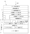
- FIG. 5 is a cross-sectional view showing an example of the X-ray imaging element 20 according to the present embodiment.
- the X-ray imaging device 20 includes a TFT circuit 22 formed on the upper layer of the a-Si substrate 21, a photodiode 23 formed on the upper layer of the TFT circuit 22, and an ITO layer on the uppermost layer of the photodiode 23.
- a transparent insulating layer 24 and a CsI phosphor layer (scintillator) 25 are formed on the transparent electrode layer 23e.
- the TFT circuit 22 includes a capacitor 22a and a gate electrode 22b, an insulating film 22c, a drain electrode 22d and a thin film silicon layer 22e, a source electrode 22f, and an insulating layer 22g on the upper layer of the a-Si substrate 21 from the lower layer.
- the photodiode 23 includes a lower electrode layer 23a, an n-type thin film silicon layer 23b, an i-type thin film silicon layer 23c, a p-type thin film silicon layer 23d, and an ITO transparent electrode layer 23e in the upper layer of the TFT circuit 22 from the lower layer.
- a signal wiring and a thin film transistor are formed on a glass substrate.
- a flexible plastic substrate is applied.
- ITO transparent electrode layer 23e since indium tin oxide (ITO) has high transmittance in the visible light region, the ITO transparent electrode layer 23e has colorless transparency or approximate transparency.
- the characteristics of ITO are electrical conductivity and transparency. By depositing a film, the charge density is improved and the conductivity is improved.
- an electron beam vapor deposition method, a physical vapor deposition method, a sputter vapor deposition method, or the like can be used.
- the X-ray imaging device 20 performs multiple laser annealing processes and flash lamp annealing processes on the silicon layers of the photodiodes 23 and the TFT circuits 22. Conversion to crystalline silicon increases the photoelectric conversion efficiency.
- a-Si substrate 21 is installed in a plasma CVD apparatus, monosilane gas, diborane gas, phosphine gas, or the like is introduced as a reaction gas, and plasma is excited by high-frequency discharge. -Si film is formed.
- the introduction gas is only monosilane gas, it becomes an i-type semiconductor, if diborane gas is mixed with monosilane gas, it becomes a p-type semiconductor, and if phosphine gas is introduced into monosilane gas, it becomes an n-type semiconductor. Further, in order to terminate unnecessary dangling bonds of Si, a film is often formed by simultaneously adding hydrogen gas.
- a high-quality thin film silicon having a high electron mobility can be obtained by forming a film at a high temperature such as a temperature of the substrate of 300 ° C. or higher. Still, the electron mobility is as low as about 1 cm 2 V / s.
- a-Si substrate 21 it is also possible to increase the electron mobility by heating the entire a-Si substrate 21 at a dull temperature, for example, 1000 ° C. or higher. At this time, not only the a-Si substrate 21 but also the substrate temperature is raised at the same time, and even if the substrate is made of glass, the softening point is exceeded, and such a process cannot be endured.
- the a-Si thin film is irradiated with powerful light all at once, the thin film is annealed at a high temperature instantaneously, and the polycrystallization of silicon is advanced, the electron mobility greatly increases to 100 cm 2 V / s or more.
- the TFT circuit 22 and the photodiode 23 having good performance can be obtained.
- an annealing process using the laser device 30 and an annealing process using the flash lamp device 40 as shown in FIG. 7 are possible.
- the laser device 30 includes a laser oscillator 31, a collimator lens 32 that converts the laser light emitted from the laser oscillator 31 into parallel light, a mask 33, and an objective lens 34.
- the objective lens 34 sets the focal length with the target silicon to be annealed as a target.
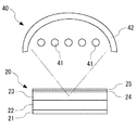
- the flash lamp device 40 includes one or more light sources 41 and a reflection mirror 42.
- the reflecting mirror 42 has a reflecting surface (parabolic surface) so that reflected light is imaged with the target silicon to be annealed as a target.
- the p-type thin film silicon layer 23d and the n-type thin film silicon layer 23b of the photodiode 23 are annealed. If necessary, an annealing process (see thick arrows in the figure) is performed so as to include regions in contact with the p-type thin film silicon layer 23d and the n-type thin film silicon layer 23b of the i-type thin film silicon layer 23c.
- the p-type thin film silicon layer 23d and the n-type thin film silicon layer 23b can be annealed to increase the conductivity, and the i-type thin film silicon layer 23c is made amorphous to improve the light absorption rate. It becomes possible.
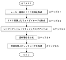
- a-Si substrate 21 is prepared, and a TFT circuit forming step (step S1) for forming a TFT circuit 22 on the upper layer is executed.
- a photodiode forming step (step S2) for forming (depositing) the photodiode 23 on the upper layer of the TFT circuit 22 is executed.
- a film of metal or resin can be used in addition to glass.
- the material for the metal film include Al, Al alloy, Fe, Fe alloy, and those laminated.
- Resin film materials include polyesters such as polyethylene terephthalate, polybutylene phthalate, and polyethylene naphthalate, polystyrene polycarbonate, polyethersulfone, polyarylate, polyimide, polycycloolefin, norbornene resin, polyfluorotrifluoroethylene, and triacetyl cellulose. Etc.
- an annealing process step (step S3) is performed in which the p-type thin film silicon layer 23d and the n-type thin film silicon layer 23b of the formed photodiode 23 are irradiated with light to perform an annealing process.
- This annealing process is performed to polycrystallize the silicon layer.
- the laser device 30 outputs 300 mJ / output to the p-type thin film silicon layer 23d and the n-type thin film silicon layer 23b having a thickness of 100 nm. Irradiation with a 10 cm 2 laser (1 shot, 23 ns) is performed.
- the p-type thin film silicon layer 23d and the n-type thin film silicon layer 23b are annealed to be polycrystallized.
- step S4 After forming the transparent insulating layer 24 (step S4), the CsI phosphor layer (scintillator) 25 is formed and the phosphor layer forming step (step S5) is executed, whereby the X-ray imaging device 20 is formed. To manufacture.
- the X-ray imaging device 20 can perform an annealing process and convert it into polycrystalline silicon to increase the photoelectric conversion efficiency, thereby making it possible to diagnose a patient with a small X-ray dose and using a resin substrate. Therefore, application to a portable type can be facilitated.
- the X-ray imaging device 20 of the present invention is not limited to the above-described embodiment, and various technical designs can be made within the technical scope described in the scope of the claims within the scope of the invention. Changed forms are included.
- the p-type thin film silicon layer 23d and the n-type thin film silicon layer 23b of the photodiode 23 are annealed.
- the layer 23c may be annealed. Thereby, the conductivity of the i-type thin film silicon layer 23c can be improved.
- the focal position of the objective lens 44 (depth direction ⁇ depth> of the photodiode 23) can be adjusted to change the place where the annealing process is performed strongly.
- the light condensing part can be strongly annealed.
- the surface can be strongly annealed, and when the light is focused on the inside, the inside can be strongly annealed.
- the annealing treatment is not limited to the silicon layer constituting the photodiode 23. Specifically, as shown in FIG. 10, the annealing treatment is performed on the thin film silicon layer 22e of the TFT circuit 22. May be. Thereby, the conductivity of the TFT circuit 22 can be improved.
- the annealing treatment is not limited to each layer unit. Specifically, as shown in FIG. 11, the lower electrode layer 23a of the photodiode 23, the n-type thin film silicon layer 23b, the i-type thin film. An annealing process may be performed across the silicon layer 23c, the p-type thin film silicon layer 23d, and the ITO transparent electrode layer 23e. As a result, the electrode portion of the pixel can be made of polycrystalline silicon and the periphery thereof can have an a-Si structure.
- the resin substrate has low heat resistance, the temperature cannot be increased during the film formation of a-Si, and the electron mobility tends to be low when compared with glass.
- the annealing process is performed by narrowing down the target, it is possible to make it difficult for such a problem related to heat resistance to occur, and a resin substrate can be used.
- the flowchart shown in FIG. 8 does not limit the procedure of the present invention, and the procedure may be added / deleted or the order may be changed without departing from the spirit and technical idea of the invention.
- the annealing process may be performed after step S5 instead of step S3 in the flowchart of FIG.
- the methods according to the above embodiments may be used in appropriate combination.
- the silicon to be annealed for example, all of the silicon shown in FIGS. 5 and 9 may be applied.
- the method for manufacturing an X-ray imaging device can diagnose a patient with a small X-ray dose by performing annealing treatment and converting it into polycrystalline silicon to increase photoelectric conversion efficiency.
- a resin substrate can be used, it has the effect that it can be easily applied to a portable type, and manufacture of an X-ray imaging device for taking a digital radiograph using X-rays. Useful for all methods.
Landscapes
- Physics & Mathematics (AREA)
- Health & Medical Sciences (AREA)
- Life Sciences & Earth Sciences (AREA)
- General Physics & Mathematics (AREA)
- High Energy & Nuclear Physics (AREA)
- Molecular Biology (AREA)
- Spectroscopy & Molecular Physics (AREA)
- Measurement Of Radiation (AREA)
- Solid State Image Pick-Up Elements (AREA)
Abstract
アニール処理を施して多結晶シリコンに変換して光電変換効率を上げることにより、少ないX線量で患者を診断することが可能なうえ、樹脂基板を使用することができるX線撮像素子の製造方法を提供する。基板の上層にTFT回路を形成するTFT回路形成ステップと、TFT回路の上層に蛍光を電気信号に変換するフォトダイオードを形成するフォトダイオード形成ステップと、TFT回路若しくはフォトダイオードを構成するシリコン層にアニール処理を施して多結晶化するアニール処理ステップと、フォトダイオードの上層にX線を蛍光に変換する蛍光体層を形成する蛍光体層形成ステップと、を含む。
Description
本発明は、X線を用いたデジタルレントゲン写真を撮影するためのX線撮像素子の製造方法に関する。
近年、X線フィルムを用いた撮影装置に置き換わるX線画像診断機器としてX線画像撮影装置の普及が拡大している。X線画像撮影装置は、X線フィルムに対してX線撮影から画像確認までの時間が非常に短いうえ、画像のダイナミックレンジが広く、X線フィルムの現像に必要な薬液も必要が無いという利点を有している。
X線画像撮影装置は、現在実用化されているものの多くが間接変換方式を採用している。このような間接型のX線画像撮影装置においては、被験者の人体(例えば、胸部)などを透過したX線画像をX線画像撮影装置に入射し、その画像情報を電気信号に変換する。この際、X線画像撮影装置は、X線を可視光に変換する蛍光変換膜によってX線を可視光に変換し、その光をマトリクス状に配置した複数の光検出器によって二次元的な画像情報として検出し、外部に電気信号として出力する。
このような間接型のX線画像撮影装置には、X線撮像素子が使用されている。このX線撮像素子は、被験者の人体を透過したX線をシンチレータを用いて光に変換し、シンチレータにより生じた光をフォトダイオードとTFTとを用いて検出する。この際、フォトダイオードとTFTとは、通常、アモルファスシリコン(以下、「a-Si」と称する)状態の薄膜シリコン膜により作成したものが知られている(例えば、特許文献1参照)。
また、このようなX線撮像素子は、可搬式とするためにカセッテ型としたものも存在するが、持ち運びの際に落としてしまうことがある。その際、X紬画像撮影装置のフォトダイオードやTFTは、ガラス基板上に成膜されていることから、そのガラス基板が割れてしまい、場合によっては装置が壊れてしまう虞があるため、ガラス基板に変えて可撓性のプラスチック基板を用いた装置も知られている(例えば、特許文献2,3参照)。
一方、撮影のために被験者の人体に対するX線の被爆量を減らすために、X線画像撮影装置の高感度化が求められている。
ところで、a-Siは、成膜温度の高い薄膜のほうが電子の移動度が高く、良好な性能を示すことが知られている。しかしながら、樹脂フィルムのような可撓性材料を用いた場合、基材の耐熱温度がガラスと比較して低いため、a-Siの成膜の際に十分に温度を上げて加熱することができないという問題が生じていた。
そこで、本発明は、上記要望に鑑みて成されたものであり、少ないX線量で患者を診断することが可能なうえ、可搬式への適用も容易とすることができるX線撮像素子及びその製造方法を提供することを目的とする。
上記課題を解決するために、本発明の一態様に係るX線撮像素子の製造方法は、基板の上層にTFT回路を形成するTFT回路形成ステップと、TFT回路の上層に蛍光を電気信号に変換するフォトダイオードを形成するフォトダイオード形成ステップと、TFT回路若しくはフォトダイオードを構成するシリコン層にアニール処理を施して多結晶化するアニール処理ステップと、フォトダイオードの上層にX線を蛍光に変換する蛍光体層を形成する蛍光体層形成ステップと、を含む。
フォトダイオードは、TFT回路の上層に、下層から、下部電極層、n型薄膜シリコン層、i型薄膜シリコン層、p型薄膜シリコン層、透明電極層、を有し、アニール処理ステップでは、p型薄膜シリコン層及びn型薄膜シリコン層の少なくともいずれか一方をターゲットとしてアニール処理を施す、ものである。
フォトダイオードは、TFT回路の上層に、下層から、下部電極層、n型薄膜シリコン層、i型薄膜シリコン層、p型薄膜シリコン層、透明電極層、を有し、アニール処理ステップでは、i型薄膜シリコン層をターゲットとしてアニール処理を施す、ものである。
TFT回路は、基板の上層に、下層から、コンデンサ及びゲート電極、絶縁膜、ドレイン電極及び薄膜シリコン層、ソース電極、絶縁層、を有し、アニール処理ステップでは、薄膜シリコン層をターゲットとしてアニール処理を施す、ものである。
フォトダイオードは、TFT回路の上層に、下層から、下部電極層、n型薄膜シリコン層、i型薄膜シリコン層、p型薄膜シリコン層、透明電極層、をこの順に有し、アニール処理ステップでは、p型薄膜シリコン層とi型薄膜シリコン層とn型薄膜シリコン層の電極部分をターゲットとしてアニール処理を施す、ものである。
なお、基板には可撓性樹脂を用いるのが好ましい。
本発明の一態様に係るX線撮像素子は、アニール処理を施して多結晶シリコンに変換して光電変換効率を上げることにより、少ないX線量で患者を診断することが可能なうえ、可搬式への適用も容易とすることができる。
次に、本発明に係る一実施の形態について図面を参照して説明する。本実施の形態として示すX線撮像素子は、間接型のデジタルX線撮影装置(digital radiography)に適用される。なお、間接方式とは、蛍光体層によりX線を受けて一旦可視光に変換し、可視光をアモルファスシリコンフォトダイオードなどにより信号電荷に変換して電荷蓄積用キャパシタに導く方式である。
図1に示すように、間接型のデジタルX線撮影装置10は、X線発生器11、臥位撮影台12、電子カセッテ13、コンソール14、モニタ15を備えている。電子カセッテ13は、コンソール14の制御に基づいて、X線発生器11から被検者Fに照射されて透過したX線を検出し、X線画像を生成する。コンソール14は、電子カセッテ13から送信されたX線画像データに各種画像処理を施し、モニタ15にX線画像Pを表示させる。
間接型のデジタルX線撮影装置10による撮影は、臥位撮影台12に仰臥した被検者Fに向けてX線発生器11により上方からX線を照射し、そのX線が被検者Fを透過して得られるX線像を電子カセッテ13で検出する。また、四肢や肘等のその他の部位の撮影では、臥位撮影台12の上に電子カセッテ13を載置して撮影することも可能である。
電子カセッテ13は、直方体形状を呈しており、例えば、半切サイズ(383.5mm×459.5mm)のフィルム用またはIP用のカセッテと同様の国際規格ISO4090:2001に準拠した外形サイズを有している。電子カセッテ13の外形サイズは、前述した半切サイズの他、四切サイズ、六切サイズ等があり、撮影部位に応じて適宜選択される。
図2に示すように、電子カセッテ13は、X線の強度を検出するためのパネル状のX線撮像素子20と信号処理回路基板16とをフレキシブルプリント基板17で電気的に接続するとともに、所定の容器18により可搬式としたものである。
図3に示すように、X線撮像素子20にはマトリクス状の多数の画素20aを有する構造のものを用いる。
電子カセッテ13は、本実施の形態において、詳細には後述するが、X線撮像素子20として、アモルファスシリコン(以下、単に「a-Si」と称する)の上層にTFTアクティブマトリクス基板(以下、TFT回路という)を形成し、このTFT回路の上層にフォトダイオード層を形成したうえでX線感応層(シンチレータ)を配置し、入射したX線をデジタルデータに変換する平面検出器(以下、単に「FPD」と称する)である。また、被検者Fを透過して照射されたX線により表されるX線画像をFPDを用いて生成するとともに、生成したX線画像を記憶する可搬型となっている。
シンチレータは、例えば、ヨウ化セシウム(CsI)蛍光体であり、X線を可視光に変換する。これにより、可視光はフォトダイオード層で光電変換され、生じた電荷はコンデンサ(後述する)に蓄積される。
X線撮像素子の信号読取時に、コンデンサの電荷は、シリコンTFT回路を通じて読み出される。電荷は、積分アンプに到達し、そこで、電荷・電圧変換され、その後、A/D変換されて、電子カセッテ13のメモリ(図示せず)にX線画像Pの画像データとして保存される。
ヨウ化セシウム(CsI)は、X線から可視光への変換率が比較的高く、蒸着によって容易に蛍光体を柱状結晶構造に形成できるため、光ガイド効果により結晶内での発光光の散乱が抑えられ、蛍光体層の厚さを厚くすることが可能である。なお、発光効率をさらに向上させるため、CsIとヨウ化ナトリウム(NaI)を任意のモル比で混合したものを、蒸着を用いてナトリウム賦活ヨウ化セシウム(CsI:Na)として堆積してもよい。また、CsIとヨウ化タリウム(TlI)を任意のモル比で混合したものを、蒸着を用いて支持体上にタリウム賦活ヨウ化セシウム(CsI:Tl)として堆積したものに、後工程としてアニールを行うことで可視変換効率を向上させ、X線蛍光体として使用してもよい。
この際、a-Siを全て多結晶化(p-Si化)してしまうと、通常のシンチレータの発光の吸収効率が低下しやすくなってしまう、このため、本実施の形態では、a-Si+多結晶(p-Si)構造を採用している。なお、アニールを穏やかに行いp-Si構造を生成させず、全てa-Si構造としても良い。
FPDとしては、シンチレータやTFT回路の配置順序によって、PSS(Penetration Side Sampling)方式のFPDと、ISS(Irradiation Side Sampling)方式と、が知られている。PSS方式は、X線の入射側から、シンチレータの下層にTFT回路を配置する方式であり、X線の入射によりシンチレータで発生する光を、シンチレータの背面(X線の入射面とは反対側の面)側で検出する。これに対し、ISS方式は、入射側から見たFPDの表裏の関係がPSS方式とは逆の関係にある。本実施の形態においては、PSS方式の場合で説明するが、ISS方式への適用も可能である。
a-Siは、蒸着法、スパッタ法、各種CVD法を用いて形成される。最も多用されているプラズマCVD法では、グロー放電により原料ガスのシラン(SiH4)、ジシラン(SiH6)を分解し、a-Si薄膜を基板上に成長させている。基板には耐熱プラスチックが用いられ、通常400℃以下で成長する。
a-Siは、原料ガスに含まれる水素が膜中に取り込まれ、シリコンの未結合手(ダングリング・ボンド)が水素で終端されるため、欠損密度が比較的小さい。ただし、a-Si膜中の電子や正孔などのキャリア移動度は、トラップ準位のため、結晶中のキャリア移動度と比べてはるかに小さな値になる。
したがって、a-Siは、製造コストが安価であるという利点があることから、TFT回路に多く用いられてきた。
このように、a-Siは、比較的簡単な加工で半導体素子を作成することができる一方、無定形さゆえに電子の移動度が低下してしまう。したがって、電子の移動度は物質の結晶構造に大きく依存する。
一方、ポリシリコン(以下、「p-Si」と称する)は、a-Siと結晶シリコン(以下、単に「c-Si」と称する)との中間に位置するような存在で、異なる方位を有する単結晶のシリコンの粒(単結晶粒)からなっている。p-Siは、粒と粒の境界部分(結晶粒界)で電子が散乱されてしまい、c-Siと比べれば移動度が低くなるものの、無定形なa-Siと比べればキャリア移動度ははるかに大きい。
しかしながら、p-Siは、情報伝達速度を高く要求するメモリ等には向いているものの、図4に示すように、シンチレータの発光領域に対する吸収効率が非常に低いという問題が生じていた。
他方、a-Siに関しても、シンチレータの通常の発光領域付近でピークを有するものの、ピーク付近の感度用帯域幅(波長幅)が非常に狭く、ピーク前後の感度差が激しいという問題が生じていた。
そこで、電子の移動度を高くすることによりX線の被曝量を抑制したいという要望に対応しつつ、シンチレータの発光に対する感度幅(ピーク幅)を拡大するため、本実施の形態においては、a-Si+p-Siを採用している。
図5は、本実施の形態に係るX線撮像素子20の一例を示す断面図である。図5において、X線撮像素子20は、a-Si基板21の上層にTFT回路22を形成した後、TFT回路22の上層にフォトダイオード23を形成したうえで、フォトダイオード23の最上層のITO透明電極層23eの上層に透明絶縁層24及びCsI蛍光体層(シンチレータ)25を形成したものである。
TFT回路22は、a-Si基板21の上層に、下層から、コンデンサ22a及びゲート電極22b、絶縁膜22c、ドレイン電極22d及び薄膜シリコン層22e、ソース電極22f、絶縁層22g、を有する。
フォトダイオード23は、TFT回路22の上層に、下層から、下部電極層23a、n型薄膜シリコン層23b、i型薄膜シリコン層23c、p型薄膜シリコン層23d、ITO透明電極層23e、を有する。
なお、これら各層の形成手順そのものに関しては、例えば、公知の液晶表示装置の製造工程に類似するTFTパネル製造工程に準じている。ただし、液晶表示装置等の場合にはガラス基板上に信号配線と薄膜トランジスタ(TFT回路)とを形成しているが、本実施の形態においては、可撓性を有するプラスチック基板が適用されている。
なお、酸化インジウムスズ(ITO)は、可視光領域の透過率が高いため、ITO透明電極層23eとしては無色透明若しくは近似する透明性を有している。ITOの特徴は電気伝導性と透明性である。蒸着成膜することで電荷密度が向上し導電性も向上する。ITO透明電極層23eは、電子ビーム蒸着法、物理気相成長法、スパッタ蒸着法などを用いることができる。
このような基本構成において、本実施の形態に係るX線撮像素子20は、フォトダイオード23やTFT回路22のシリコン層に対して、レーザアニール処理やフラッシュランプアニ一ル処理を施すことによって、多結晶シリコンに変換して光電変換効率を上げるようにしている。
一般に、a-Siの成謨では、a-Si基板21をプラズマCVD装置に設置した後、反応ガスとして、モノシランガスやジボランガス、ホスフィンガスなどを導入して、高周波放電によりプラズマを励起して、a-Siの成膜を行う。
この際、導入ガスをモノシランガスのみとすると、i型半導体となり、モノシランガスにジボランガスを混合するとp型半導体となり、モノシランガスにホスフィンガスを導入すると、n型半導体になる。また、不要なSiのダングリングボンドを終末させるため、水素ガスを同時に添加して成膜することもよく行われている。
a-Siの成膜では、成膜時の基板の温度は一般には300℃以上など、高温で成膜したほうが電子移動度の高い、良質な薄膜シリコンが得られることが知られているが、それでも電子移動度は、1cm2V/s程度と低い。
a-Si基板21の全体を単鈍に、例えば、1000℃以上に加熱することによっても、電子移動度を上昇させることは可能である。この際、a-Si基板21だけでなく、同時に基板温度も上昇させてしまい、基板がガラスであっても軟化点を超えてしまい、このようなプロセスには耐えられない。
そこで、a-Si薄膜に、強力な光を一気に照射し、薄膜を瞬時に高温にしてアニール処理し、シリコンの多結晶化を進めると、電子移動度を100cm2V/s以上と、大きく上昇させることができ、良好な性能のTFT回路22やフォトダイオード23を得ることができる。
ところで、アニール処理を施すには、例えば、図6に示すように、レーザ装置30を用いたアニール処理と、図7に示すように、フラッシュランプ装置40を用いたアニール処理とが可能である。
図6に示すように、レーザ装置30は、レーザ発振器31と、レーザ発振器31から出射したレーザ光を平行光とするコリメートレンズ32と、マスク33と、対物レンズ34と、を有する。ここで、対物レンズ34は、アニール処理する対象シリコンをターゲットとして焦点距離を設定している。
図7に示すように、フラッシュランプ装置40は、一つ以上の光源41と、反射ミラー42と、を有する。ここで、反射ミラー42は、アニール処理する対象シリコンをターゲットとして反射光を結像するよう、反射面(放物面)を設定している。
アニール処理するターゲットのシリコンとしては、例えば、図5に示すように、フォトダイオード23のp型薄膜シリコン層23d及びn型薄膜シリコン層23bにアニール処理を施す。なお、必要に応じて、i型薄膜シリコン層23cのp型薄膜シリコン層23d並びにn型薄膜シリコン層23bと接する領域を含むようにアニール処理(図の太両矢印参照)を施す。
これにより、p型薄膜シリコン層23dとn型薄膜シリコン層23bとにアニール処理を施すことにより伝導度を上げることができるうえ、i型薄膜シリコン層23cをアモルファス状態にして光吸収率を向上させることが可能となる。
<X線撮像素子20の製造方法>
次に、X線撮像素子20の製造方法について図8のフロー図に基づいて説明する。
次に、X線撮像素子20の製造方法について図8のフロー図に基づいて説明する。
まず、a-Si基板21を用意し、その上層にTFT回路22を形成するTFT回路形成ステップ(ステップS1)を実行する。次に、TFT回路22の上層にフォトダイオード23を形成(成膜)するフォトダイオード形成ステップ(ステップS2)を実行する。
なお、a-Si基板21としては、ガラスの他に金属や樹脂のフィルムを用いることができる。金属フィルムの材料としては、AlやAl合金、FeやFe合金およびそれらが積層されたものなどが挙げられる。樹脂フィルムの材料としては、ポリエチレンテレフタレート、ポリブチレンフタレート、ポリエチレンナフタレート等のポリエステルや、ポリスチレンポリカーボネート、ポリエーテルスルホン、ポリアリレート、ポリイミド、ポリシクロオレフィン、ノルボルネン樹脂、ポリフロロトリフルオロエチレン、トリアセチルセルロース等が挙げられる。
そして、一様に、成膜されたフォトダイオード23のp型薄膜シリコン層23d及びn型薄膜シリコン層23bに光を照射してアニール処理を施すアニール処理ステップ(ステップS3)を実行する。このアニール処理は、シリコン層を多結晶化するために行うものであり、例えば、レーザ装置30から、膜厚100nmのp型薄膜シリコン層23d及びn型薄膜シリコン層23bに対して、出力300mJ/cm2のレーザを10ショット(1ショット23ns)照射するものである。
これにより、p型薄膜シリコン層23d及びn型薄膜シリコン層23bがアニール処理されて多結晶化する。
その次に、透明絶縁層24を形成(ステップS4)した後に、CsI蛍光体層(シンチレータ)25を形成して蛍光体層形成ステップ(ステップS5)を実行することにより、X線撮像素子20を製造する。
このようにして、X線撮像素子20は、アニール処理を施して多結晶シリコンに変換して光電変換効率を上げることにより、少ないX線量で患者を診断することが可能なうえ、樹脂基板を使用することができることから、可搬式への適用も容易とすることができる。
ところで、本発明のX線撮像素子20は、上記の実施の形態に限定されるものでなく、特許請求の範囲に記載した技術的範囲には、発明の要旨を逸脱しない範囲内で種々、設計変更した形態が含まれる。
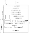
例えば、上記実施の形態では、フォトダイオード23のp型薄膜シリコン層23d及びn型薄膜シリコン層23bにアニール処理を施したが、例えば、図9に示すように、フォトダイオード23のi型薄膜シリコン層23cにアニール処理を施してもよい。これにより、i型薄膜シリコン層23cの伝導率を向上することができる。
このアニール処理の際に、例えば、対物レンズ44の焦点位置(フォトダイオード23の深さ方向<深度>)を調整し、アニール処理を強力に行う場所を変えることもできる。これにより、光の集光部分を強くアニール処理することができる。例えば、表面に集光すると表面を強くアニール処理することができ、内部に集光すると内部を強くアニールしょりすることができる。
また、アニール処理を施すのは、フォトダイオード23を構成するシリコン層に限定されるものでもない、具体的には、図10に示すように、TFT回路22の薄膜シリコン層22eにアニール処理を施してもよい。これにより、TFT回路22の伝導度を向上することができる。
さらに、アニール処理を施すのは、各層単位に限定されるものでもない、具体的には、図11に示すように、フォトダイオード23の下部電極層23a、n型薄膜シリコン層23b、i型薄膜シリコン層23c、p型薄膜シリコン層23d、ITO透明電極層23e、に跨ってアニール処理を施してもよい。これにより、画素の電極部分を多結晶化シリコンとし、その周囲はa-Si構造とすることができる。
さらに、上記実施の形態では、通常のガラス基板を用いても有効であるが、特に、可撓性の樹脂基板を用いた際に有効である。すなわち、樹脂基板は耐熱性が低いため、a-Siの成膜時に温度を高温とすることができず、ガラスと比較した場合に電子移動度が低くなり易いからである。これに対し、本実施の形態では、ターゲットを絞ってアニール処理を施すため、このような耐熱性に関する不具合を発生し難くすることができ、樹脂基板を用いることができる。
また、図8に示すフローチャートは、本発明の手順を限定するものではなく、発明の趣旨及び技術的思想を逸脱しない範囲内で手順の追加・削除又は順番の変更等をしてもよい。例えば、アニール処理のタイミングは、図8のフロー図において、ステップS3のタイミングではなく、ステップS5の後に行ってもよい。
また、以上既に述べた以外にも、上記実施の形態による手法を適宜組み合わせて利用しても良い。例えば、アニール処理を施すシリコン(ターゲットシリコン)は、例えば、図5及び図9に示したシリコンの全てを適用してもよい。
その他、本発明は、その趣旨を逸脱しない範囲内において、種々の変更が加えられて実施されるものである。
以上説明したように、本発明に係るX線撮像素子の製造方法は、アニール処理を施して多結晶シリコンに変換して光電変換効率を上げることにより、少ないX線量で患者を診断することが可能なうえ、樹脂基板を使用することができることから、可搬式への適用も容易とすることができるという効果を有し、X線を用いたデジタルレントゲン写真を撮影するためのX線撮像素子の製造方法全般に有用である。
20 X線撮像素子
21 アモルファスシリコン基板
22 TFT回路
23 フォトダイオード
25 CsI蛍光体層(シンチレータ)
21 アモルファスシリコン基板
22 TFT回路
23 フォトダイオード
25 CsI蛍光体層(シンチレータ)
Claims (6)
- 基板の上層にTFT回路を形成するTFT回路形成ステップと、
前記TFT回路の上層に蛍光を電気信号に変換するフォトダイオードを形成するフォトダイオード形成ステップと、
前記TFT回路若しくは前記フォトダイオードを構成するシリコン層にアニール処理を施して多結晶化するアニール処理ステップと、
前記フォトダイオードの上層にX線を蛍光に変換する蛍光体層を形成する蛍光体層形成ステップと、
を含むX線撮像素子の製造方法。 - 前記フォトダイオードは、
前記TFT回路の上層に、下層から、下部電極層、n型薄膜シリコン層、i型薄膜シリコン層、p型薄膜シリコン層、透明電極層、を有し、
前記アニール処理ステップでは、
前記p型薄膜シリコン層及び前記n型薄膜シリコン層の少なくともいずれか一方をターゲットとしてアニール処理を施す
ことを特徴とする請求項1に記載のX線撮像素子の製造方法。 - 前記フォトダイオードは、
前記TFT回路の上層に、下層から、下部電極層、n型薄膜シリコン層、i型薄膜シリコン層、p型薄膜シリコン層、透明電極層、を有し、
前記アニール処理ステップでは、
前記i型薄膜シリコン層をターゲットとしてアニール処理を施す
ことを特徴とする請求項1又は請求項2に記載のX線撮像素子の製造方法。 - 前記TFT回路は、
前記基板の上層に、下層から、コンデンサ及びゲート電極、絶縁膜、ドレイン電極及び薄膜シリコン層、ソース電極、絶縁層、を有し、
前記アニール処理ステップでは、
前記薄膜シリコン層をターゲットとしてアニール処理を施す
ことを特徴とする請求項1乃至請求項3のいずれか1の請求項に記載のX線撮像素子の製造方法。 - 前記フォトダイオードは、
前記TFT回路の上層に、下層から、下部電極層、n型薄膜シリコン層、i型薄膜シリコン層、p型薄膜シリコン層、透明電極層、をこの順に有し、
前記アニール処理ステップでは、
前記p型薄膜シリコン層と前記i型薄膜シリコン層と前記n型薄膜シリコン層の電極部分をターゲットとしてアニール処理を施す
ことを特徴とする請求項1乃至請求項4のいずれか1の請求項に記載のX線撮像素子の製造方法。 - 前記基板に可撓性樹脂を用いることを特徴とする請求項1乃至請求項5のいずれか1の請求項に記載のX線撮像素子の製造方法。
Applications Claiming Priority (2)
| Application Number | Priority Date | Filing Date | Title |
|---|---|---|---|
| JP2015209511A JP2017083218A (ja) | 2015-10-26 | 2015-10-26 | X線撮像素子の製造方法 |
| JP2015-209511 | 2015-10-26 |
Publications (1)
| Publication Number | Publication Date |
|---|---|
| WO2017073174A1 true WO2017073174A1 (ja) | 2017-05-04 |
Family
ID=58631505
Family Applications (1)
| Application Number | Title | Priority Date | Filing Date |
|---|---|---|---|
| PCT/JP2016/076273 Ceased WO2017073174A1 (ja) | 2015-10-26 | 2016-09-07 | X線撮像素子の製造方法 |
Country Status (2)
| Country | Link |
|---|---|
| JP (1) | JP2017083218A (ja) |
| WO (1) | WO2017073174A1 (ja) |
Citations (5)
| Publication number | Priority date | Publication date | Assignee | Title |
|---|---|---|---|---|
| JPH11307756A (ja) * | 1998-02-20 | 1999-11-05 | Canon Inc | 光電変換装置および放射線読取装置 |
| JP2010153834A (ja) * | 2008-11-28 | 2010-07-08 | Semiconductor Energy Lab Co Ltd | フォトセンサ及び表示装置 |
| JP2011066070A (ja) * | 2009-09-15 | 2011-03-31 | Idemitsu Kosan Co Ltd | 多結晶薄膜、その成膜方法、及び薄膜トランジスタ |
| JP2012247327A (ja) * | 2011-05-30 | 2012-12-13 | Sony Corp | 放射線撮像装置および放射線撮像表示システム |
| JP2012256812A (ja) * | 2010-08-06 | 2012-12-27 | Semiconductor Energy Lab Co Ltd | 固体撮像装置、半導体表示装置 |
-
2015
- 2015-10-26 JP JP2015209511A patent/JP2017083218A/ja active Pending
-
2016
- 2016-09-07 WO PCT/JP2016/076273 patent/WO2017073174A1/ja not_active Ceased
Patent Citations (5)
| Publication number | Priority date | Publication date | Assignee | Title |
|---|---|---|---|---|
| JPH11307756A (ja) * | 1998-02-20 | 1999-11-05 | Canon Inc | 光電変換装置および放射線読取装置 |
| JP2010153834A (ja) * | 2008-11-28 | 2010-07-08 | Semiconductor Energy Lab Co Ltd | フォトセンサ及び表示装置 |
| JP2011066070A (ja) * | 2009-09-15 | 2011-03-31 | Idemitsu Kosan Co Ltd | 多結晶薄膜、その成膜方法、及び薄膜トランジスタ |
| JP2012256812A (ja) * | 2010-08-06 | 2012-12-27 | Semiconductor Energy Lab Co Ltd | 固体撮像装置、半導体表示装置 |
| JP2012247327A (ja) * | 2011-05-30 | 2012-12-13 | Sony Corp | 放射線撮像装置および放射線撮像表示システム |
Also Published As
| Publication number | Publication date |
|---|---|
| JP2017083218A (ja) | 2017-05-18 |
Similar Documents
| Publication | Publication Date | Title |
|---|---|---|
| JP5043374B2 (ja) | 変換装置、放射線検出装置、及び放射線検出システム | |
| KR101257699B1 (ko) | 방사선 디텍터 및 그 제조방법 | |
| CN103543461B (zh) | 辐射检测器及其制造方法 | |
| JP5830867B2 (ja) | 放射線撮像装置および放射線撮像表示システム | |
| JP7048588B2 (ja) | ハイブリッド・アクティブマトリクス・フラットパネル検出器システムおよび方法 | |
| JP2008051793A (ja) | 放射線検出装置及びシンチレータパネル | |
| JP2007329434A (ja) | 放射線撮像装置及び放射線撮像システム | |
| JP2005114731A (ja) | 後方照射を有する半導体放射線撮像装置 | |
| JP2014508397A (ja) | 反射能力を含む高性能x線画像化アレイのための装置および方法 | |
| WO2016138725A1 (zh) | 阵列基板及其制作方法、x射线平板探测器、摄像系统 | |
| JP2003107163A (ja) | 加熱装置を備えて提供されるx線検出器 | |
| US9006662B2 (en) | Radiological image detection device | |
| US6989539B2 (en) | Flat dynamic radiation detector | |
| US10386505B2 (en) | Scintillator, scintillator panel, radiation detector and method of manufacturing scintillator | |
| JP2016048168A (ja) | 放射線検出器、撮像装置、および撮像システム | |
| CN105378507B (zh) | 辐射检测器、闪烁体板和制造它们的方法 | |
| JP2017083218A (ja) | X線撮像素子の製造方法 | |
| EP3070500B1 (en) | Radiation detector and method for manufacturing radiation detector | |
| WO2017134896A1 (ja) | X線撮像素子の製造方法 | |
| US8415634B2 (en) | Apparatus and method for detecting radiation | |
| US8536553B2 (en) | Apparatus and method for detecting radiation | |
| JP2004167075A (ja) | 放射線撮像装置及び放射線撮像方法 | |
| JP5789223B2 (ja) | 放射線撮像装置及び放射線撮像システム | |
| CN116806370A (zh) | 探测基板及射线探测器 | |
| JP2007159790A (ja) | 放射線撮影装置及び放射線撮影システム |
Legal Events
| Date | Code | Title | Description |
|---|---|---|---|
| 121 | Ep: the epo has been informed by wipo that ep was designated in this application |
Ref document number: 16859411 Country of ref document: EP Kind code of ref document: A1 |
|
| NENP | Non-entry into the national phase |
Ref country code: DE |
|
| 122 | Ep: pct application non-entry in european phase |
Ref document number: 16859411 Country of ref document: EP Kind code of ref document: A1 |