WO2017069022A1 - 酸化物半導体 - Google Patents
酸化物半導体 Download PDFInfo
- Publication number
- WO2017069022A1 WO2017069022A1 PCT/JP2016/080205 JP2016080205W WO2017069022A1 WO 2017069022 A1 WO2017069022 A1 WO 2017069022A1 JP 2016080205 W JP2016080205 W JP 2016080205W WO 2017069022 A1 WO2017069022 A1 WO 2017069022A1
- Authority
- WO
- WIPO (PCT)
- Prior art keywords
- oxide
- oxide semiconductor
- semiconductor
- type
- pyrochlore structure
- Prior art date
- Legal status (The legal status is an assumption and is not a legal conclusion. Google has not performed a legal analysis and makes no representation as to the accuracy of the status listed.)
- Ceased
Links
Images


Classifications
-
- C—CHEMISTRY; METALLURGY
- C01—INORGANIC CHEMISTRY
- C01G—COMPOUNDS CONTAINING METALS NOT COVERED BY SUBCLASSES C01D OR C01F
- C01G33/00—Compounds of niobium
- C01G33/006—Compounds containing niobium, with or without oxygen or hydrogen, and containing two or more other elements
-
- C—CHEMISTRY; METALLURGY
- C01—INORGANIC CHEMISTRY
- C01G—COMPOUNDS CONTAINING METALS NOT COVERED BY SUBCLASSES C01D OR C01F
- C01G33/00—Compounds of niobium
-
- C—CHEMISTRY; METALLURGY
- C04—CEMENTS; CONCRETE; ARTIFICIAL STONE; CERAMICS; REFRACTORIES
- C04B—LIME, MAGNESIA; SLAG; CEMENTS; COMPOSITIONS THEREOF, e.g. MORTARS, CONCRETE OR LIKE BUILDING MATERIALS; ARTIFICIAL STONE; CERAMICS; REFRACTORIES; TREATMENT OF NATURAL STONE
- C04B35/00—Shaped ceramic products characterised by their composition; Ceramics compositions; Processing powders of inorganic compounds preparatory to the manufacturing of ceramic products
- C04B35/01—Shaped ceramic products characterised by their composition; Ceramics compositions; Processing powders of inorganic compounds preparatory to the manufacturing of ceramic products based on oxide ceramics
- C04B35/453—Shaped ceramic products characterised by their composition; Ceramics compositions; Processing powders of inorganic compounds preparatory to the manufacturing of ceramic products based on oxide ceramics based on zinc, tin, or bismuth oxides or solid solutions thereof with other oxides, e.g. zincates, stannates or bismuthates
- C04B35/457—Shaped ceramic products characterised by their composition; Ceramics compositions; Processing powders of inorganic compounds preparatory to the manufacturing of ceramic products based on oxide ceramics based on zinc, tin, or bismuth oxides or solid solutions thereof with other oxides, e.g. zincates, stannates or bismuthates based on tin oxides or stannates
-
- C—CHEMISTRY; METALLURGY
- C04—CEMENTS; CONCRETE; ARTIFICIAL STONE; CERAMICS; REFRACTORIES
- C04B—LIME, MAGNESIA; SLAG; CEMENTS; COMPOSITIONS THEREOF, e.g. MORTARS, CONCRETE OR LIKE BUILDING MATERIALS; ARTIFICIAL STONE; CERAMICS; REFRACTORIES; TREATMENT OF NATURAL STONE
- C04B35/00—Shaped ceramic products characterised by their composition; Ceramics compositions; Processing powders of inorganic compounds preparatory to the manufacturing of ceramic products
- C04B35/01—Shaped ceramic products characterised by their composition; Ceramics compositions; Processing powders of inorganic compounds preparatory to the manufacturing of ceramic products based on oxide ceramics
- C04B35/495—Shaped ceramic products characterised by their composition; Ceramics compositions; Processing powders of inorganic compounds preparatory to the manufacturing of ceramic products based on oxide ceramics based on vanadium, niobium, tantalum, molybdenum or tungsten oxides or solid solutions thereof with other oxides, e.g. vanadates, niobates, tantalates, molybdates or tungstates
-
- C—CHEMISTRY; METALLURGY
- C04—CEMENTS; CONCRETE; ARTIFICIAL STONE; CERAMICS; REFRACTORIES
- C04B—LIME, MAGNESIA; SLAG; CEMENTS; COMPOSITIONS THEREOF, e.g. MORTARS, CONCRETE OR LIKE BUILDING MATERIALS; ARTIFICIAL STONE; CERAMICS; REFRACTORIES; TREATMENT OF NATURAL STONE
- C04B35/00—Shaped ceramic products characterised by their composition; Ceramics compositions; Processing powders of inorganic compounds preparatory to the manufacturing of ceramic products
- C04B35/622—Forming processes; Processing powders of inorganic compounds preparatory to the manufacturing of ceramic products
- C04B35/626—Preparing or treating the powders individually or as batches ; preparing or treating macroscopic reinforcing agents for ceramic products, e.g. fibres; mechanical aspects section B
- C04B35/62605—Treating the starting powders individually or as mixtures
- C04B35/6261—Milling
- C04B35/6262—Milling of calcined, sintered clinker or ceramics
-
- H—ELECTRICITY
- H10—SEMICONDUCTOR DEVICES; ELECTRIC SOLID-STATE DEVICES NOT OTHERWISE PROVIDED FOR
- H10D—INORGANIC ELECTRIC SEMICONDUCTOR DEVICES
- H10D62/00—Semiconductor bodies, or regions thereof, of devices having potential barriers
- H10D62/80—Semiconductor bodies, or regions thereof, of devices having potential barriers characterised by the materials
-
- C—CHEMISTRY; METALLURGY
- C01—INORGANIC CHEMISTRY
- C01P—INDEXING SCHEME RELATING TO STRUCTURAL AND PHYSICAL ASPECTS OF SOLID INORGANIC COMPOUNDS
- C01P2002/00—Crystal-structural characteristics
- C01P2002/30—Three-dimensional structures
- C01P2002/36—Three-dimensional structures pyrochlore-type (A2B2O7)
-
- C—CHEMISTRY; METALLURGY
- C01—INORGANIC CHEMISTRY
- C01P—INDEXING SCHEME RELATING TO STRUCTURAL AND PHYSICAL ASPECTS OF SOLID INORGANIC COMPOUNDS
- C01P2002/00—Crystal-structural characteristics
- C01P2002/70—Crystal-structural characteristics defined by measured X-ray, neutron or electron diffraction data
- C01P2002/72—Crystal-structural characteristics defined by measured X-ray, neutron or electron diffraction data by d-values or two theta-values, e.g. as X-ray diagram
-
- C—CHEMISTRY; METALLURGY
- C01—INORGANIC CHEMISTRY
- C01P—INDEXING SCHEME RELATING TO STRUCTURAL AND PHYSICAL ASPECTS OF SOLID INORGANIC COMPOUNDS
- C01P2006/00—Physical properties of inorganic compounds
- C01P2006/40—Electric properties
-
- C—CHEMISTRY; METALLURGY
- C04—CEMENTS; CONCRETE; ARTIFICIAL STONE; CERAMICS; REFRACTORIES
- C04B—LIME, MAGNESIA; SLAG; CEMENTS; COMPOSITIONS THEREOF, e.g. MORTARS, CONCRETE OR LIKE BUILDING MATERIALS; ARTIFICIAL STONE; CERAMICS; REFRACTORIES; TREATMENT OF NATURAL STONE
- C04B2235/00—Aspects relating to ceramic starting mixtures or sintered ceramic products
- C04B2235/02—Composition of constituents of the starting material or of secondary phases of the final product
- C04B2235/30—Constituents and secondary phases not being of a fibrous nature
- C04B2235/32—Metal oxides, mixed metal oxides, or oxide-forming salts thereof, e.g. carbonates, nitrates, (oxy)hydroxides, chlorides
- C04B2235/3231—Refractory metal oxides, their mixed metal oxides, or oxide-forming salts thereof
- C04B2235/3251—Niobium oxides, niobates, tantalum oxides, tantalates, or oxide-forming salts thereof
-
- C—CHEMISTRY; METALLURGY
- C04—CEMENTS; CONCRETE; ARTIFICIAL STONE; CERAMICS; REFRACTORIES
- C04B—LIME, MAGNESIA; SLAG; CEMENTS; COMPOSITIONS THEREOF, e.g. MORTARS, CONCRETE OR LIKE BUILDING MATERIALS; ARTIFICIAL STONE; CERAMICS; REFRACTORIES; TREATMENT OF NATURAL STONE
- C04B2235/00—Aspects relating to ceramic starting mixtures or sintered ceramic products
- C04B2235/02—Composition of constituents of the starting material or of secondary phases of the final product
- C04B2235/30—Constituents and secondary phases not being of a fibrous nature
- C04B2235/32—Metal oxides, mixed metal oxides, or oxide-forming salts thereof, e.g. carbonates, nitrates, (oxy)hydroxides, chlorides
- C04B2235/3293—Tin oxides, stannates or oxide forming salts thereof, e.g. indium tin oxide [ITO]
-
- C—CHEMISTRY; METALLURGY
- C04—CEMENTS; CONCRETE; ARTIFICIAL STONE; CERAMICS; REFRACTORIES
- C04B—LIME, MAGNESIA; SLAG; CEMENTS; COMPOSITIONS THEREOF, e.g. MORTARS, CONCRETE OR LIKE BUILDING MATERIALS; ARTIFICIAL STONE; CERAMICS; REFRACTORIES; TREATMENT OF NATURAL STONE
- C04B2235/00—Aspects relating to ceramic starting mixtures or sintered ceramic products
- C04B2235/60—Aspects relating to the preparation, properties or mechanical treatment of green bodies or pre-forms
- C04B2235/604—Pressing at temperatures other than sintering temperatures
-
- C—CHEMISTRY; METALLURGY
- C04—CEMENTS; CONCRETE; ARTIFICIAL STONE; CERAMICS; REFRACTORIES
- C04B—LIME, MAGNESIA; SLAG; CEMENTS; COMPOSITIONS THEREOF, e.g. MORTARS, CONCRETE OR LIKE BUILDING MATERIALS; ARTIFICIAL STONE; CERAMICS; REFRACTORIES; TREATMENT OF NATURAL STONE
- C04B2235/00—Aspects relating to ceramic starting mixtures or sintered ceramic products
- C04B2235/65—Aspects relating to heat treatments of ceramic bodies such as green ceramics or pre-sintered ceramics, e.g. burning, sintering or melting processes
- C04B2235/658—Atmosphere during thermal treatment
- C04B2235/6586—Processes characterised by the flow of gas
-
- C—CHEMISTRY; METALLURGY
- C04—CEMENTS; CONCRETE; ARTIFICIAL STONE; CERAMICS; REFRACTORIES
- C04B—LIME, MAGNESIA; SLAG; CEMENTS; COMPOSITIONS THEREOF, e.g. MORTARS, CONCRETE OR LIKE BUILDING MATERIALS; ARTIFICIAL STONE; CERAMICS; REFRACTORIES; TREATMENT OF NATURAL STONE
- C04B2235/00—Aspects relating to ceramic starting mixtures or sintered ceramic products
- C04B2235/70—Aspects relating to sintered or melt-casted ceramic products
- C04B2235/74—Physical characteristics
- C04B2235/76—Crystal structural characteristics, e.g. symmetry
-
- C—CHEMISTRY; METALLURGY
- C04—CEMENTS; CONCRETE; ARTIFICIAL STONE; CERAMICS; REFRACTORIES
- C04B—LIME, MAGNESIA; SLAG; CEMENTS; COMPOSITIONS THEREOF, e.g. MORTARS, CONCRETE OR LIKE BUILDING MATERIALS; ARTIFICIAL STONE; CERAMICS; REFRACTORIES; TREATMENT OF NATURAL STONE
- C04B2235/00—Aspects relating to ceramic starting mixtures or sintered ceramic products
- C04B2235/70—Aspects relating to sintered or melt-casted ceramic products
- C04B2235/74—Physical characteristics
- C04B2235/76—Crystal structural characteristics, e.g. symmetry
- C04B2235/762—Cubic symmetry, e.g. beta-SiC
-
- C—CHEMISTRY; METALLURGY
- C04—CEMENTS; CONCRETE; ARTIFICIAL STONE; CERAMICS; REFRACTORIES
- C04B—LIME, MAGNESIA; SLAG; CEMENTS; COMPOSITIONS THEREOF, e.g. MORTARS, CONCRETE OR LIKE BUILDING MATERIALS; ARTIFICIAL STONE; CERAMICS; REFRACTORIES; TREATMENT OF NATURAL STONE
- C04B2235/00—Aspects relating to ceramic starting mixtures or sintered ceramic products
- C04B2235/70—Aspects relating to sintered or melt-casted ceramic products
- C04B2235/74—Physical characteristics
- C04B2235/79—Non-stoichiometric products, e.g. perovskites (ABO3) with an A/B-ratio other than 1
-
- H—ELECTRICITY
- H10—SEMICONDUCTOR DEVICES; ELECTRIC SOLID-STATE DEVICES NOT OTHERWISE PROVIDED FOR
- H10D—INORGANIC ELECTRIC SEMICONDUCTOR DEVICES
- H10D30/00—Field-effect transistors [FET]
- H10D30/60—Insulated-gate field-effect transistors [IGFET]
- H10D30/67—Thin-film transistors [TFT]
- H10D30/674—Thin-film transistors [TFT] characterised by the active materials
- H10D30/6755—Oxide semiconductors, e.g. zinc oxide, copper aluminium oxide or cadmium stannate
Definitions
- the present invention relates to an oxide semiconductor composed of an oxide composite, and more particularly to an oxide semiconductor capable of realizing p-type semiconductor characteristics.
- transparent conductor materials and transparent semiconductor materials having high transparency in the visible light region and high electrical conductivity are known as oxide composites, and are widely used for transparent electrodes and the like.
- transparent semiconductors In 2 O 3 , ZnO, SnO 2 , and Sn-added In 2 O 3 , impurities added to these base materials, Al-added ZnO, Ga-added ZnO, Sb-added SnO 2 , and F-added SnO are used. 2 and the like are known, but these are all n-type semiconductors in which electrons serve as charge carriers.
- semiconductors include p-type semiconductors that use holes as charge carriers. If n-type and p-type semiconductors that are transparent in the visible light region are prepared, forming a pn junction makes it possible to produce a diode, transistor, solar cell, or the like that is transparent in the visible light region.
- Cu 2 O, NiO, and the like are already known as p-type semiconductors, but are not transparent because they absorb light in the visible light region and have strong coloration. Since 1990, research and development of transparent p-type conductors has been promoted, and several new transparent p-type conductors have been reported.
- a compound having a delafossite structure has low hole mobility.
- the oxychalcogenide compound has a considerably high mobility and hole concentration, but is oxidized in the air atmosphere, so that the characteristic deterioration is remarkable.
- zinc oxide is an n-type semiconductor that originally uses electrons as charge carriers, it is necessary to reduce the concentration of structural defects that generate electrons to the limit and introduce structural defects that express p-type semiconductor characteristics such as nitrogen. There is. For this reason, it is difficult to produce zinc oxide having p-type semiconductor characteristics and poor reproducibility due to the difficulty in generating n-type structural defects accompanying the introduction of p-type structural defects and reducing the concentration of n-type structural defects. Therefore, it is difficult to realize a transparent p-type semiconductor suitable for an electronic device.
- An oxide semiconductor is expected as a semiconductor material resistant to an oxidation reaction in an atmosphere containing oxygen.
- it is difficult to realize p-type conductivity with an oxide. This is because in the oxide, electrons at the upper end of the valence band are localized on oxygen ions.
- a metal d-orbital component is introduced at the upper end of the valence band
- a p-orbital component of a chalcogen element is introduced at the upper end of the valence band. The presence is reduced.
- Non-Patent Document 1 a metal oxide having a pyrochlore structure represented by the composition formula Sn 2 Nb 2 O 7 is composed of a 5s component of Sn at the upper end of the valence band.
- Patent Document 2 reports a photocatalyst of an oxide complex composed of Sn 2 Nb 2 O 7 (oxide semiconductor) and titanium oxide.
- the photocatalyst is composed of an oxide composite having a junction made of different kinds of oxide semiconductors having different energy levels of electrons at the bottom of the conduction band and electrons at the top of the valence band.
- Patent Document 3 discloses ABO 4 + x (where ⁇ 0.25 ⁇ x ⁇ 0.5, A ions are Sn elements, B ions are one or more elements selected from Nb and Ta), and fluorite. Pyrochlore-related structure in which oxygen vacancies are regularly present and oxygen vacancies in the pyrochlore structure where cations are regularly arranged are filled with oxygen, either ⁇ -PbO 2 -related structures or rutile-related structures A photocatalyst having a structure has been reported. In contrast to the photocatalyst, as Comparative Example 1, it has been reported that a product of Sn 2 Nb 2 O 7 pyrochlore structure which has not been oxidized has almost no photocatalytic property.
- the present invention is intended to solve these problems, and an object of the present invention is to provide a novel oxide semiconductor that has low light absorption in the visible light region and can realize high charge carrier mobility. And It is another object of the present invention to provide an oxide semiconductor that exhibits p-type semiconductor characteristics.
- the present invention has the following features in order to achieve the above object.
- the present invention is an oxide semiconductor comprising an oxide composite having a pyrochlore structure containing Sn and Nb, and the composition ratio Sn / Nb is 0.81 ⁇ Sn / Nb ⁇ 1.0. To do.
- the oxide semiconductor of the present invention is characterized in that holes serve as charge carriers.
- a transparent and high mobility semiconductor having a wide gap can be realized in an oxide semiconductor.
- a p-type oxide semiconductor was realized by the oxide semiconductor of the present invention. Since the oxide semiconductor of the present invention has a pyrochlore structure containing Sn and Nb, a wide gap with a band gap of 2.2 eV can be realized, and thus has high transparency in the visible light region.
- the oxide semiconductor of the present invention is composed of a 5s component of Sn at the upper end of the valence band.
- the semiconductor of the present invention is made of an oxide and has weather resistance
- an electronic device having excellent weather resistance can be realized by forming a pn junction of the p-type oxide semiconductor and the n-type oxide semiconductor of the present invention. .
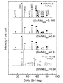
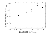
- the figure which shows the X-ray-diffraction pattern in case the analysis composition value (Sn / Nb) after is 0.68, 0.81, 0.91, 0.998 in 1st Embodiment. is there. It is a figure showing the relationship between the preparation composition value (Sn / Nb) before and the analysis composition value (Sn / Nb) after after baking in 1st Embodiment. It is a figure which shows the change of the specific resistance with respect to the analysis composition value (Sn / Nb) after in 1st Embodiment. It is a figure which shows the change of the density
- the present inventor conducted research and development focusing on the fact that semiconductor characteristics are influenced by the composition ratio of Sn / Nb in an oxide composite having a pyrochlore structure, and has excellent semiconductor characteristics. Thus, an oxide semiconductor having semiconductor characteristics has been obtained.
- SnO having a small bandgap in which the upper end portion of the valence band is composed of the Sn orbital of Sn is formed by a double oxide formation with Nb 2 O 5.
- the crystal structure has a pyrochlore structure, and the Sn / Nb composition ratio Sn / Nb is 0.81 ⁇ Sn /Nb ⁇ 1.0 is a semiconductor.
- the oxide semiconductor according to the embodiment of the present invention is Sn 2 Nb 2 O 7 having a small composition with respect to the stoichiometric composition ratio so as to form holes that are p-type charge carriers.
- Non-Patent Document 2 in a compound described as Sn 2 Nb 2 O 7 with a simple composition formula, if two structural defects are represented, Sn 2-x (Nb 2-y Sn y ) O 7-x-0.5y .
- No oxide composite having a pyrochlore structure has developed p-type semiconductor characteristics, including Non-Patent Document 2 above. It generates a -2 valence defect V '' Sn simultaneously generates +2 oxygen vacancy V ⁇ ⁇ O, so resulting in charge compensation, the expression of p-type conduction is not obtained due to holes generated Therefore, it is considered.
- the amount of V ′′ Sn and V ⁇ O produced is considered to depend on the temperature and the atmospheric gas conditions when the oxide composite is produced. In the present invention, the generation of V ′′ Sn is controlled by changing the composition ratio Sn / Nb at the time of sample preparation, while V ⁇ O is controlled by the atmospheric gas conditions.
- n-type semiconductor suitable for forming a pn junction with the p-type semiconductor of this embodiment In 2 O 3 , ZnO, SnO 2 , Sn-doped In 2 O 3 in which impurities are added to these base materials, Al Additive ZnO, Ga-added ZnO, Sb-added SnO 2 , F-added SnO 2, and the like.
- ZnO can be manufactured from an insulator to a semiconductor due to easy control of carrier concentration, It is preferable from the viewpoints of ease of use and lack of scarcity of raw materials.
- an oxide semiconductor including an oxide complex having a pyrochlore structure containing Sn and Nb is described.
- the oxide composite having a pyrochlore structure composed of Sn, Nb and oxygen the characteristics corresponding to the composition ratio Sn / Nb were examined.
- the composition ratio Sn / Nb is 0.81 ⁇ Sn / Nb ⁇ 1.0, which exhibits a pyrochlore structure and exhibits p-type semiconductor characteristics using holes as charge carriers.
- Example 1 What weighed SnO powder (purity 99.5%, high purity chemical laboratory) and Nb 2 O 5 (purity 99.9%, high purity chemical laboratory) was put in an agate mortar and ethanol (Japanese Wet mixing was carried out for about 1 hour while adding Kogyo Pharmaceutical Co., Ltd. At this time, SnO and Nb 2 O 5 have a ratio of Sn to Nb (Sn / Nb) of 0.95, 1.00, 1.10, 1.20, 1.30, 1.40 as atomic ratios. It mixed so that it might become. This charged composition value is hereinafter referred to as “(Sn / Nb) before ”. Table 1 summarizes the amount of reagent weighed during sample preparation. A sample having (Sn / Nb) before of 0.85 corresponds to Comparative Example 1 described later.
- the mixture was allowed to stand overnight at room temperature to dry the ethanol, and the powder divided into approximately six equal parts was uniaxially pressed (diameter: 15 mm, 170 MPa) to produce six disk-shaped green compacts.
- the green compact was placed on an alumina boat, placed in an electric furnace having an alumina furnace core tube having a diameter of 50 mm and a length of 800 mm, and calcined at 900 ° C. for 4 hours while flowing a nitrogen gas at a flow rate of 150 ml / min.
- the calcined green compact was crushed in an agate mortar, and an aqueous polyvinyl alcohol solution as a binder was 2 wt. % And mixed with ethanol and left to dry overnight at room temperature.
- the particle diameter was adjusted to 212 ⁇ m or less by sieving, and uniaxial pressing (diameter: 15 mm, 170 MPa) was followed by hydrostatic pressing (285 MPa) to produce a molded body having a diameter of about 15 mm and a thickness of about 1.2 mm.
- the obtained molded body was placed on an alumina boat and subjected to main firing at 1100 ° C. for 4 hours while flowing nitrogen gas (flow rate: 150 ml / min). As shown in Table 2, which will be described later, Sample Nos.
- Comparative Example 1 is an example different from Example 1 only in that SnO and Nb 2 O 5 are mixed so that the ratio of Sn to Nb (Sn / Nb) is 0.85 in terms of the number of atoms. Comparative Example 1 (Sample No. 6) was produced under the same conditions as in Example 1, except that the flow rate of nitrogen gas (N 2 gas) during firing was 150 ml / min.
- Example 2 was different from Example 1 only in the flow rate of nitrogen gas (N 2 gas) during firing, and the other production conditions were the same. As shown in Table 2 described later, Sample Nos. 7 to 12 have charge composition values ((Sn / Nb) before ) of 1.40, 1.30, 1.20, 1.10, 1.00, 0, respectively. .95, and a nitrogen gas (N 2 gas) flow rate during firing was 50 ml / min.
- Example 3 was different from Example 1 only in the flow rate of nitrogen gas (N 2 gas) during firing, and the other production conditions were the same. As shown in Table 2 to be described later, sample numbers 13 and 14 are charged composition values ((Sn / Nb) before ) of 1.30 and 1.00, respectively, and the nitrogen gas (N 2 gas) flow rate during firing is as follows. This sample was prepared under the condition of 20 ml / min.
- FIG. 1 shows changes in the X-ray diffraction pattern of the Sn 2 Nb 2 O 7 sample by (Sn / Nb) after .
- the horizontal axis in FIG. 1 is the diffraction angle 2 ⁇ with respect to the incident angle ⁇ using CuK ⁇ rays.
- (Sn / Nb) In the X-ray diffraction pattern when after is 0.81, 0.91, and 0.998, peaks (black circles) belonging to Sn 2 Nb 2 O 7 having a pyrochlore structure belonging to a cubic system are shown. (222) (400) (440) (622), etc.) shown remarkably.
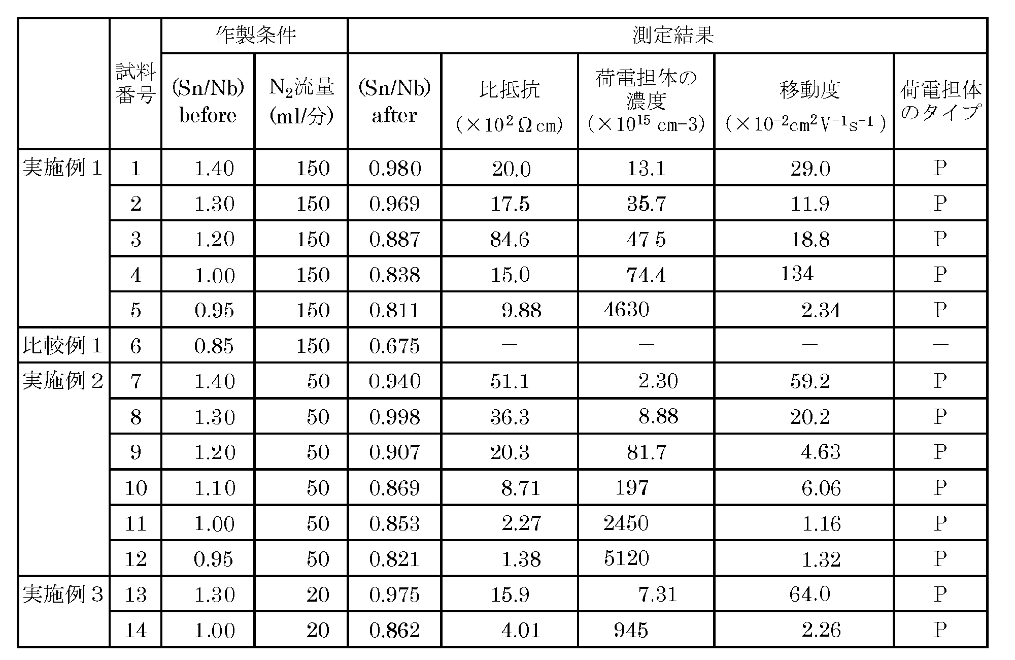
- Table 2 shows analytical composition values (Sn / Nb) after and electrical measurement results (ratio) of samples prepared by changing the charged composition value ((Sn / Nb) before ) and the nitrogen gas (N 2 gas) flow rate during firing. (Resistance, charge carrier concentration, mobility, type of charge carrier).
- FIG. 2 shows a plot of sample composition values ((Sn / Nb) before ) and analytical composition values after firing ((Sn / Nb) after ).
- the feed composition value was between 0.85 ⁇ (Sn / Nb) before ⁇ 1.3
- (Sn / Nb) before 1.4
- the value of (Sn / Nb) after was decreased. This is presumably because excess Sn that does not constitute the pyrochlore structure preferentially evaporated during firing.
- FIG. 3 shows a change in specific resistance with respect to (Sn / Nb) after .
- FIG. 3 shows specific resistance values in the range of (Sn / Nb) after approximately 0.81 to approximately 1.0.
- the specific resistance of the sample decreases as (Sn / Nb) after decreases, indicating that there is a good correlation between the specific resistance and (Sn / Nb) after .
- the nitrogen flow rate during firing is 150 ml / min. (Black circle), 50 ml / min. (Black triangle), 20 ml / min. The case of (white circle) is shown.
- the error bar in the figure indicates the standard deviation ⁇ .
- FIG. 4 shows changes in the concentration of the charge carrier with respect to (Sn / Nb) after .
- the nitrogen flow rate during firing is 150 ml / min. (Black circle), 50 ml / min. (Black triangle), 20 ml / min. The case of (white circle) is shown.
- the error bar indicates the standard deviation ⁇ .
- (Sn / Nb) after is in the range of about 0.81 to about 1.0, the variation among the samples is large, and the variation is larger than the result of the specific resistance in FIG. Nb) It can be seen that the concentration of the charge carrier increases with a decrease in after .
- the compound ratio Sn / Nb is 0.81 in the compound represented by Sn 2 Nb 2 O 7 by a simple composition formula based on the identification of the crystal phase by X-ray diffraction and the evaluation of the electrical characteristics by Hall effect measurement.
- ⁇ Sn / Nb ⁇ 1.0
- Thin-film oxide semiconductors can be produced by sputtering, heating, electron beam deposition, ion plating, and other oxide film production methods such as spin coating and spray coating using solutions as starting materials. Can be manufactured by technology.
- the oxide semiconductor of the present invention can realize a p-type semiconductor, a pn junction can be realized by an n-type semiconductor and a p-type semiconductor that are transparent in the visible light region, and widely used in devices such as a transmissive display and a transparent transistor. Can be industrially useful.
Landscapes
- Chemical & Material Sciences (AREA)
- Engineering & Computer Science (AREA)
- Organic Chemistry (AREA)
- Ceramic Engineering (AREA)
- Manufacturing & Machinery (AREA)
- Materials Engineering (AREA)
- Structural Engineering (AREA)
- Inorganic Chemistry (AREA)
- Inorganic Compounds Of Heavy Metals (AREA)
- Thin Film Transistor (AREA)
Abstract
Description
本実施の形態では、Sn及びNbを含むパイロクロア構造を有する酸化物複合体からなる酸化物半導体について説明する。Sn、Nb及び酸素からなるパイロクロア構造を有する酸化物複合体において、組成比Sn/Nbに対応する特性を調べた。以下に示すように、組成比Sn/Nbが0.81≦Sn/Nb<1.0で、パイロクロア構造を示し、かつ正孔を荷電担体とするp型半導体特性を発現する。
(実施例1)
SnO粉末(株式会社高純度化学研究所 純度99.5%)とNb2O5(株式会社高純度化学研究所 純度99.9%)を秤量したものを、メノウ製乳鉢に入れ、エタノール(和光純薬株式会社 特級)を加えながら約1時間湿式混合した。このとき、SnOとNb2O5は、SnとNbの比(Sn/Nb)が原子数比で0.95、1.00、1.10、1.20、1.30、1.40となるように混合した。この仕込み組成値を以後「(Sn/Nb)before」と表記する。試料調整時の試薬秤量の量を表1にまとめて示す。なお、(Sn/Nb)beforeが0.85の試料は、後述する比較例1に対応する。

比較例1は、SnOとNb2O5を、SnとNbの比(Sn/Nb)が原子数比で0.85となるように混合した点でのみ実施例1と異なる例である。比較例1(試料番号6)は、作製条件を実施例1と同様にして、焼成時の窒素ガス(N2ガス)流量が150ml/分の条件で作製した。
実施例2は、実施例1とは、焼成時の窒素ガス(N2ガス)流量のみが異なり、他の作製条件は同様にして実施した。後述する表2に示すように、試料番号7乃至12は、仕込み組成値((Sn/Nb)before)がそれぞれ1.40、1.30、1.20、1.10、1.00、0.95で、焼成時の窒素ガス(N2ガス)流量が50ml/分の条件で作製した試料である。
実施例3は、実施例1とは、焼成時の窒素ガス(N2ガス)流量のみが異なり、他の作製条件は同様にして実施した。後述する表2に示すように、試料番号13及び14は、仕込み組成値((Sn/Nb)before)がそれぞれ1.30、1.00で、焼成時の窒素ガス(N2ガス)流量が20ml/分の条件で作製した試料である。
実施例1、2、3及び比較例1で得られた試料の結晶構造の同定は、X線回折装置(パナリティカル X’Pert Pro MRD)により行った。焼成後のSn/Nbの組成比の見積もりは波長分散型蛍光X線分析装置(リガクZSX)を用いた。焼成後の分析組成値は「(Sn/Nb)after」と表記する。試料の電気特性の評価は、円形試料の四隅に金電極を蒸着した試料を準備し、ファンデルパウ配置によりホール効果測定装置(東陽テクニカ Resitest 8310)を用いて行った。すべての測定は室温で行った。
Claims (2)
- Sn及びNbを含むパイロクロア構造を有する酸化物複合体からなり、組成比Sn/Nbが0.81≦Sn/Nb<1.0であることを特徴とする酸化物半導体。
- 正孔が荷電担体となることを特徴とする請求項1記載の酸化物半導体。
Priority Applications (2)
| Application Number | Priority Date | Filing Date | Title |
|---|---|---|---|
| US15/769,612 US20180305219A1 (en) | 2015-10-20 | 2016-10-12 | Oxide semiconductor |
| JP2017546510A JP6562321B2 (ja) | 2015-10-20 | 2016-10-12 | 酸化物半導体 |
Applications Claiming Priority (2)
| Application Number | Priority Date | Filing Date | Title |
|---|---|---|---|
| JP2015206351 | 2015-10-20 | ||
| JP2015-206351 | 2015-10-20 |
Publications (1)
| Publication Number | Publication Date |
|---|---|
| WO2017069022A1 true WO2017069022A1 (ja) | 2017-04-27 |
Family
ID=58557435
Family Applications (1)
| Application Number | Title | Priority Date | Filing Date |
|---|---|---|---|
| PCT/JP2016/080205 Ceased WO2017069022A1 (ja) | 2015-10-20 | 2016-10-12 | 酸化物半導体 |
Country Status (3)
| Country | Link |
|---|---|
| US (1) | US20180305219A1 (ja) |
| JP (1) | JP6562321B2 (ja) |
| WO (1) | WO2017069022A1 (ja) |
Cited By (1)
| Publication number | Priority date | Publication date | Assignee | Title |
|---|---|---|---|---|
| US11239322B2 (en) * | 2017-02-23 | 2022-02-01 | National Institute Of Advanced Industrial Science And Technology | P-type oxide semiconductor and semiconductor device having pyrochlore structure |
Families Citing this family (2)
| Publication number | Priority date | Publication date | Assignee | Title |
|---|---|---|---|---|
| CN113033950B (zh) * | 2021-02-03 | 2023-06-23 | 生态环境部华南环境科学研究所 | 基于多个排放源项的石油化工行业挥发性有机物源成分谱的建立方法 |
| TWI769031B (zh) | 2021-07-29 | 2022-06-21 | 力晶積成電子製造股份有限公司 | 鐵電記憶體結構 |
Citations (3)
| Publication number | Priority date | Publication date | Assignee | Title |
|---|---|---|---|---|
| JPS58219703A (ja) * | 1982-06-01 | 1983-12-21 | イ−・アイ・デユ・ポン・ドウ・ヌム−ル・アンド・カンパニ− | 酸化錫を含む導電相の製造方法 |
| JP2003117407A (ja) * | 2001-08-08 | 2003-04-22 | Sumitomo Metal Mining Co Ltd | 可視光域でも触媒活性を有する光触媒 |
| JP2004344733A (ja) * | 2003-05-21 | 2004-12-09 | Sumitomo Metal Mining Co Ltd | 複合酸化物から成る光触媒とその製造方法 |
-
2016
- 2016-10-12 WO PCT/JP2016/080205 patent/WO2017069022A1/ja not_active Ceased
- 2016-10-12 US US15/769,612 patent/US20180305219A1/en not_active Abandoned
- 2016-10-12 JP JP2017546510A patent/JP6562321B2/ja not_active Expired - Fee Related
Patent Citations (3)
| Publication number | Priority date | Publication date | Assignee | Title |
|---|---|---|---|---|
| JPS58219703A (ja) * | 1982-06-01 | 1983-12-21 | イ−・アイ・デユ・ポン・ドウ・ヌム−ル・アンド・カンパニ− | 酸化錫を含む導電相の製造方法 |
| JP2003117407A (ja) * | 2001-08-08 | 2003-04-22 | Sumitomo Metal Mining Co Ltd | 可視光域でも触媒活性を有する光触媒 |
| JP2004344733A (ja) * | 2003-05-21 | 2004-12-09 | Sumitomo Metal Mining Co Ltd | 複合酸化物から成る光触媒とその製造方法 |
Non-Patent Citations (2)
| Title |
|---|
| CRUZ, LUISA PAULA ET AL.: "Pyrochlore-type tin niobate, Acta Crystallographica", SECTION C: CRYSTAL STRUCTURE COMMUNICATIONS, vol. C57, no. 9, 2001, pages 1001 - 1003, ISSN: 0108-2701 * |
| KATAYAMA, SHOTA ET AL., JOURNAL OF CRYSTAL GROWTH, vol. 416, 15 April 2015 (2015-04-15), pages 126 - 129, XP029176029, ISSN: 0022-0248 * |
Cited By (1)
| Publication number | Priority date | Publication date | Assignee | Title |
|---|---|---|---|---|
| US11239322B2 (en) * | 2017-02-23 | 2022-02-01 | National Institute Of Advanced Industrial Science And Technology | P-type oxide semiconductor and semiconductor device having pyrochlore structure |
Also Published As
| Publication number | Publication date |
|---|---|
| JP6562321B2 (ja) | 2019-08-21 |
| JPWO2017069022A1 (ja) | 2018-07-19 |
| US20180305219A1 (en) | 2018-10-25 |
Similar Documents
| Publication | Publication Date | Title |
|---|---|---|
| Han et al. | Structural and optical properties of rock-salt Cd1− xZnxO thin films prepared by thermal decomposition of electrodeposited Cd1− xZnxO2 | |
| Kumar et al. | Reduction in the tilting of oxygen octahedron and its effect on bandgap with La doping in SrSnO3 | |
| JP6562321B2 (ja) | 酸化物半導体 | |
| JP2014040331A (ja) | 亜鉛錫酸化物の製造方法 | |
| JPWO2017043586A1 (ja) | 金属オキシハライドを原料とした金属サルファハライド及び/又は金属セレンハライドの合成方法、並びに、それを利用した半導体部材の製造方法 | |
| Vijayalakshmi et al. | Novel two-step process for the fabrication of MnO2 nanostructures on tantalum for enhanced electrochemical H2O2 detection | |
| Hamao et al. | Synthesis and crystal structure of fluorite-type La2. 4Zr1. 2Ta0. 4O7: a precursor oxide for low temperature formation of garnet-type Li6. 5La3Zr1. 5Ta0. 5O12 | |
| Zhou et al. | High throughput discovery of enhanced visible photoactivity in Fe–Cr vanadate solar fuels photoanodes | |
| TWI649264B (zh) | 氧化物半導體及半導體裝置 | |
| Shaili et al. | Revealing the impact of strontium doping on the optical, electronic and electrical properties of nanostructured 2H-CuFeO 2 delafossite thin films | |
| US20120037857A1 (en) | Method for Manufacturing a Powder for the Production of P-Type Transparent Conductive Films | |
| Al Bacha et al. | Advances in oxychalcogenide materials for hydrogen evolution photocatalysis in aqueous media | |
| Roelsgaard et al. | The hydrothermal synthesis, crystal structure and electrochemical properties of MnSb 2 O 4 | |
| Lv et al. | Gamma-Bi 4 V 2 O 11–a layered oxide material for ion exchange in aqueous media | |
| JP7037197B2 (ja) | 酸化物半導体及び半導体装置 | |
| WO2017204202A1 (ja) | 酸化物半導体 | |
| Peiteado et al. | Preparation of ZnO-SnO2 ceramic materials by a coprecipitation method | |
| Besprozvannykh et al. | SrO-Bi2O3-Fe2O3-Based Composites: Synthesis and Electrophysical Properties | |
| Gofurov et al. | Zr-Doped Bivo4 Photoanode Deposited by Co-Sputtering to Enhance Photocatalytic Performance | |
| Vijayaprasath et al. | A comparative study on pure and Mg doped ZnO nano structured thin films | |
| RU2554952C2 (ru) | КОМПОЗИТНЫЙ ТВЕРДЫЙ ЭЛЕКТРОЛИТ НА ОСНОВЕ ФАЗ, КРИСТАЛЛИЗУЮЩИХСЯ В СИСТЕМЕ Bi2O3-BaO-Fe2О3, И СПОСОБ ЕГО ПОЛУЧЕНИЯ (ВАРИАНТЫ) | |
| Kharroubi et al. | Synthesis and Properties of (Bi, Cd)-doped CuMn2O4 thin films by sol-gel dip-coating method | |
| Kamel et al. | Tunability of transport properties in semi-exfoliated Ag x CoO 2− δ (0.4< x< 1) crystals | |
| Koo et al. | Metal Perovskite Sulphides and Composites: Properties, Synthesis, Chemistry, and Applications | |
| Hamdi et al. | Synthesis, structural and electrical characterizations of Er0. 33Sr1. 67Ni0. 8Cu0. 2O4− δ |
Legal Events
| Date | Code | Title | Description |
|---|---|---|---|
| 121 | Ep: the epo has been informed by wipo that ep was designated in this application |
Ref document number: 16857337 Country of ref document: EP Kind code of ref document: A1 |
|
| ENP | Entry into the national phase |
Ref document number: 2017546510 Country of ref document: JP Kind code of ref document: A |
|
| WWE | Wipo information: entry into national phase |
Ref document number: 15769612 Country of ref document: US |
|
| NENP | Non-entry into the national phase |
Ref country code: DE |
|
| 122 | Ep: pct application non-entry in european phase |
Ref document number: 16857337 Country of ref document: EP Kind code of ref document: A1 |