WO2017057555A1 - 回路基板およびその設計方法 - Google Patents
回路基板およびその設計方法 Download PDFInfo
- Publication number
- WO2017057555A1 WO2017057555A1 PCT/JP2016/078793 JP2016078793W WO2017057555A1 WO 2017057555 A1 WO2017057555 A1 WO 2017057555A1 JP 2016078793 W JP2016078793 W JP 2016078793W WO 2017057555 A1 WO2017057555 A1 WO 2017057555A1
- Authority
- WO
- WIPO (PCT)
- Prior art keywords
- circuit board
- pad electrodes
- via conductors
- pad
- electronic component
- Prior art date
- Legal status (The legal status is an assumption and is not a legal conclusion. Google has not performed a legal analysis and makes no representation as to the accuracy of the status listed.)
- Ceased
Links
Images




Classifications
-
- H—ELECTRICITY
- H05—ELECTRIC TECHNIQUES NOT OTHERWISE PROVIDED FOR
- H05K—PRINTED CIRCUITS; CASINGS OR CONSTRUCTIONAL DETAILS OF ELECTRIC APPARATUS; MANUFACTURE OF ASSEMBLAGES OF ELECTRICAL COMPONENTS
- H05K1/00—Printed circuits
- H05K1/02—Details
-
- H—ELECTRICITY
- H05—ELECTRIC TECHNIQUES NOT OTHERWISE PROVIDED FOR
- H05K—PRINTED CIRCUITS; CASINGS OR CONSTRUCTIONAL DETAILS OF ELECTRIC APPARATUS; MANUFACTURE OF ASSEMBLAGES OF ELECTRICAL COMPONENTS
- H05K3/00—Apparatus or processes for manufacturing printed circuits
-
- H—ELECTRICITY
- H10—SEMICONDUCTOR DEVICES; ELECTRIC SOLID-STATE DEVICES NOT OTHERWISE PROVIDED FOR
- H10W—GENERIC PACKAGES, INTERCONNECTIONS, CONNECTORS OR OTHER CONSTRUCTIONAL DETAILS OF DEVICES COVERED BY CLASS H10
- H10W70/00—Package substrates; Interposers; Redistribution layers [RDL]
- H10W70/60—Insulating or insulated package substrates; Interposers; Redistribution layers
-
- H—ELECTRICITY
- H10—SEMICONDUCTOR DEVICES; ELECTRIC SOLID-STATE DEVICES NOT OTHERWISE PROVIDED FOR
- H10W—GENERIC PACKAGES, INTERCONNECTIONS, CONNECTORS OR OTHER CONSTRUCTIONAL DETAILS OF DEVICES COVERED BY CLASS H10
- H10W70/00—Package substrates; Interposers; Redistribution layers [RDL]
- H10W70/60—Insulating or insulated package substrates; Interposers; Redistribution layers
- H10W70/67—Insulating or insulated package substrates; Interposers; Redistribution layers characterised by their insulating layers or insulating parts
- H10W70/68—Shapes or dispositions thereof
-
- H—ELECTRICITY
- H10—SEMICONDUCTOR DEVICES; ELECTRIC SOLID-STATE DEVICES NOT OTHERWISE PROVIDED FOR
- H10W—GENERIC PACKAGES, INTERCONNECTIONS, CONNECTORS OR OTHER CONSTRUCTIONAL DETAILS OF DEVICES COVERED BY CLASS H10
- H10W90/00—Package configurations
- H10W90/701—Package configurations characterised by the relative positions of pads or connectors relative to package parts
- H10W90/721—Package configurations characterised by the relative positions of pads or connectors relative to package parts of bump connectors
- H10W90/724—Package configurations characterised by the relative positions of pads or connectors relative to package parts of bump connectors between a chip and a stacked insulating package substrate, interposer or RDL
Definitions
- the present invention relates to a circuit board and a design method thereof, and more particularly, to a circuit board for mounting an electronic component and a design method thereof.
- Patent Document 1 a circuit board for mounting an electronic component such as a semiconductor element is known (for example, Patent Document 1).
- Patent Document 1 discloses a circuit board having a conductor pattern (pad electrode) formed on a main surface of a substrate body so as to be connected to a via conductor provided in the substrate body.
- Various chip parts, a high frequency filter, a transmission filter and a reception filter as a diplexer, a power amplification semiconductor element, and the like are joined to the circuit board using solder (paragraphs 0006 to 0009 of Patent Document 1). reference).
- FIG. 1 is a schematic cross-sectional view of a circuit board 101 in a comparative example for explaining the problems of the prior art.
- the circuit board 101 includes a board body 110 and a plurality of via conductors v1 to v provided in the board body 110 so as to be exposed from the inside of the board body 110 to the main surface 110a.
- v4 and two pad electrodes p1 and p2 provided on the main surface 110a of the substrate body 110 so as to be connected to the via conductors v1 and v2, respectively.
- Via conductors v1 to v4 are provided on the substrate body 110 in accordance with the positional relationship of a plurality of external terminals (or bumps 6) formed on the electronic component 5.
- the centers of the via conductors v1 and v2 are coincident with the centers of the pad electrodes p1 and p2, respectively.
- the electronic component 5 is bonded to the pad electrodes p1 and p2 of the circuit board 101 via the bumps 6.
- the present invention provides a circuit board and a design method thereof that can reduce the occurrence of short-circuit defects even when pad electrodes are formed out of alignment.
- a circuit board includes a board body, and a plurality of via conductors provided in the board body so as to be exposed from the inside of the board body to the main surface.
- a circuit board including a plurality of pad electrodes provided on a main surface of the substrate body so as to be connected to each of the plurality of via conductors. The distance between the centers of at least two pad electrodes of the plurality of pad electrodes is larger than the distance between the centers of the two via conductors connected to each of the pad electrodes, and the distance between the two pad electrodes. Is greater than or equal to the interval between the two via conductors.
- the distance between the centers of the two pad electrodes is larger than the distance between the centers of the two via conductors connected to each of the pad electrodes, and the distance between the two pad electrodes is equal to or greater than the distance between the two via conductors. Therefore, even when the pad electrode is formed so as to be displaced with respect to a desired position, it is possible to suppress contact with the via conductor located in the displaced direction. As a result, it is possible to reduce the occurrence of short-circuit defects caused by the circuit board.
- the two pad electrodes may be formed so that at least a part of the two via conductors is exposed.
- the pad electrode connected to the exposed via conductor is formed on the exposed side with respect to the desired position, the pad electrode is shifted in the shifted direction. It can suppress contacting the via conductor located. As a result, it is possible to reduce the occurrence of short-circuit defects caused by the circuit board.
- the two pad electrodes are in directions away from the via conductors located next to the via conductors connected to the two pad electrodes, respectively, and adjacent to an interval between adjacent via conductors. It may be provided apart from the via conductor located.
- the electronic component may be a flip chip component connected to the pad electrode using a bump.
- the two pad electrodes are respectively located in the vicinity of two opposing sides of the outer periphery of the electronic component. May be located.
- the two pad electrodes are located at two of the four corners of the electronic component, respectively. It may be.
- the two pads are defined when a via conductor group including a plurality of adjacent via conductors at a distance within twice the minimum pitch of the plurality of via conductors is defined in plan view of the circuit board.
- An electrode may be connected to each of the two via conductors located outside the via conductor group.
- the two pads are defined when a via conductor group including a plurality of adjacent via conductors at a distance within twice the minimum pitch of the plurality of via conductors is defined in plan view of the circuit board.
- An electrode may be connected to each of the two via conductors located at an outer corner of the via conductor group.
- a circuit board design method is configured such that the substrate is connected to each of a plurality of via conductors exposed on the main surface of the substrate body.
- circuit board By designing the circuit board in this way, even when the pad electrode is formed with a deviation from a desired position, it is possible to suppress contact with the via conductor located in the displaced direction. As a result, it is possible to reduce the occurrence of short-circuit defects caused by the circuit board.
- FIG. 1 is a schematic diagram of a cross-section of a circuit board in a comparative example, where (a) shows a state where the pad electrode is at a desired position, and (b) shows a state where the pad electrode is formed shifted from the desired position.
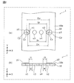
- FIG. 2A and 2B are schematic views of the circuit board according to the first embodiment, where FIG. 2A is a plan view and FIG. 2B is a cross-sectional view.
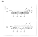
- 3A and 3B are schematic views of a cross section of the circuit board according to the first embodiment, where FIG. 3A is a state where the pad electrode is in a desired position, and FIG. 3B is a state where the pad electrode is shifted from the desired position. It is a figure which shows a state.
- FIG. 1 is a schematic diagram of a cross-section of a circuit board in a comparative example, where (a) shows a state where the pad electrode is at a desired position, and (b) shows a state where the pad electrode is formed shifted from the
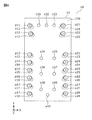
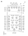
- FIG. 4 is a plan view of a circuit board according to the second embodiment.
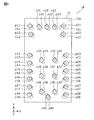
- FIG. 5 is a plan view of a circuit board according to a modification of the second embodiment.
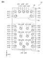
- FIG. 6 is a plan view when electronic components are mounted on the circuit board according to the third embodiment.
- FIG. 7 is a diagram for explaining the circuit board according to the third embodiment from another aspect.
- FIG. 8 is a plan view when electronic components are mounted on the circuit board according to the fourth embodiment.
- FIG. 9 is a diagram for explaining the circuit board according to the fourth embodiment from another aspect.
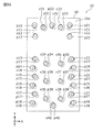
- FIG. 10 is a plan view of a circuit board according to the fifth embodiment.
- 11A and 11B are diagrams for explaining the positional relationship between the via conductor and the pad electrode shown in FIG. 10.
- FIG. 11A is a diagram according to the fifth embodiment
- FIG. 11B is a diagram of a comparative example.
- the circuit board according to the present embodiment is a circuit board for mounting electronic components such as semiconductor elements.
- the electronic component is, for example, a flip-chip component, and is connected to the circuit board via a plurality of bumps (bonding materials).
- FIG. 2 is a schematic diagram of the circuit board 1 according to the first embodiment, where (a) is a plan view and (b) is a cross-sectional view.
- (a) is a plan view
- (b) is a cross-sectional view.
- the same type of components are shown in the same pattern, the reference numerals are omitted as appropriate, and strictly speaking, components in different cross sections may be shown in the same drawing and described.
- the circuit board 1 includes a board body 10, a plurality of via conductors v (v1 to v4) provided inside the board body 10, and a main surface 10a of the board body 10. Are provided with a plurality of pad electrodes p (p1, p2).
- the substrate body 10 for example, electrical elements such as an inductor, a capacitor, and a resistor, and lead wirings for connecting these electrical elements are formed (not shown).
- the material of the substrate body 10 is, for example, LTCC ceramics (Low Temperature Co-fired Ceramics).
- LTCC ceramics Low Temperature Co-fired Ceramics
- an alumina substrate can also be used.
- the via conductor v is provided so as to be exposed from the inside of the substrate body 10 to the main surface 10a.
- the via conductor v is provided on the substrate body 10 in accordance with the positional relationship of a plurality of external terminals (or bumps) formed on the electronic component 5 (see FIG. 3A).
- the via conductor v has a circular shape in plan view.
- a material having high conductivity is used, for example, silver, copper tin, nickel, gold, or an alloy selected from these materials.
- the pad electrode p is an electrode for connecting the electronic component 5 to the circuit board 1.
- the pad electrodes p1 and p2 are formed so as to be connected to the via conductors v1 and v2 located outside the plurality of via conductors v, respectively.
- the shape of the pad electrode p is circular in plan view, and the area thereof is larger than the area of the via conductor v.
- a material having a high bonding property with the bump 6 and the via conductor v and a high conductivity is used as the material of the pad electrode p.
- the material is selected from silver, copper, tin, nickel, gold, or these materials. An alloy or the like is used.
- the center Cp of each of the pad electrodes p1 and p2 in the direction in which the pad electrodes p1 and p2 are arranged is the respective of the via conductors v1 and v2. It is designed to be located on the outer side (minus side and plus side in the X direction) with respect to the center Cv.
- the center distance Dp between the two pad electrodes p1 and p2 is made larger than the center distance Dv between the two via conductors v1 and v2 connected to the pad electrodes p1 and p2, respectively.
- the interval Ip between the two pad electrodes p1 and p2 is set to be equal to or greater than the interval Iv between the two via conductors v1 and v2. Further, the interval Ip between the two pad electrodes p1 and p2 is made smaller than the center distance Dv between the two via conductors v1 and v2.
- the shape of the pad electrode p and the via conductor v shown in FIG. 2A may be elliptical, arcuate or angular.
- the centers Cp of the pad electrodes p1 and p2 in the present embodiment are the centroids of the pad electrodes p1 and p2, respectively, and the centers Cv of the via conductors v1 and v2 are the respective centers of the via conductors v1 and v2.
- the interval Ip between the two pad electrodes p1 and p2 in this embodiment means the shortest distance between these pad electrodes, and the interval Iv between the two via conductors v1 and v2 indicates the shortest distance between these via conductors. means.
- the pad electrodes p1 and p2 are formed so that parts of the via conductors v1 and v2 are exposed.
- the pad electrode p1 is positioned in a direction away from the via conductor v3 located next to the via conductor v1 connected to the pad electrode p1 (minus side in the X direction). is doing.
- the distance i1 between the pad electrode p1 and the via conductor v3 is designed to be larger than the distance i2 between the adjacent via conductors v1 and v3.
- the pad electrode p2 is located in a direction away from the via conductor v4 located next to the via conductor v2 connected to the pad electrode p2 (plus side in the X direction).
- the distance i3 between the pad electrode p2 and the via conductor v4 is designed to be larger than the distance i4 between the adjacent via conductors v2 and v4.
- FIG. 3A is a view showing a state where the pad electrodes p1 and p2 are at desired positions
- FIG. 3B is a view showing a state where the pad electrodes p1 and p2 are formed shifted from the desired positions.
- the electronic component 5 is bonded to the circuit board 1 via bumps 6.
- the pad electrode p1 and p2 are formed to be shifted to the right side (plus side in the X direction)
- the interval i1 between the pad electrode p1 and the via conductor v3 is larger than the interval i2
- the pad electrode p1 is less likely to contact the adjacent via conductor v3.
- the interval i3 between the original pad electrode p2 and the via conductor v4 is the interval. Since it is larger than i4, it becomes difficult for the pad electrode p2 to contact the adjacent via conductor v4. As a result, the occurrence of short-circuit defects in the product (circuit module) caused by the circuit board 1 is reduced.
- the pad electrodes p1 and p2 are both formed to be shifted to the right or left. However, only the pad electrode p1 is formed to be shifted to the right or only the pad electrode p2 is formed to be shifted to the left. Even if it is a case, the said effect can be exhibited.
- a plurality of via holes formed in a ceramic green sheet are filled with a conductive paste to form a ceramic green sheet having a plurality of via conductor patterns. Then, these ceramic green sheets are stacked and integrated to form an unfired laminate block.
- a plurality of pad electrode patterns connected to each of the plurality of via conductor patterns are formed by screen-printing the surface of the green laminate block.
- the formation position of the pad electrode pattern is such that, in the direction in which the two pad electrode patterns are arranged (for example, the X direction) among the plurality of pad electrode patterns, the center of each of the two pad electrode patterns becomes the two pad electrode patterns. It is designed in advance so as to be located outside the center of each of the two via conductor patterns to be connected. In addition, the inner edges of the two pad electrode patterns are designed in advance so as to be located on the outer side of the inner edges of the two via conductor patterns.
- the unfired laminated body block is fired in a lump to produce the circuit board 1 having the via conductor v and the pad electrode p.
- An electronic component 5 is mounted on the manufactured circuit board 1. Thereafter, the circuit board 1 is resin-sealed so as to cover the electronic component 5 and is put into a reflow furnace.
- the center distance Dp between the two pad electrodes p1 and p2 is larger than the center distance Dv between the two via conductors v1 and v2 connected to the pad electrodes p1 and p2, respectively.
- the interval Ip between the two pad electrodes p1 and p2 is greater than or equal to the interval Iv between the two via conductors v1 and v2. Therefore, even when the pad electrodes p1 and p2 are formed so as to be shifted in the direction in which the two via conductors v are arranged with respect to a desired position, the pad electrodes p1 and p2 are in contact with the via conductors v positioned in the shifted direction. Can be suppressed. As a result, it is possible to reduce the occurrence of short-circuit defects caused by the circuit board 1.
- the two pad electrodes p1 and p2 are designed so that at least a part of the two via conductors v1 and v2 is exposed. Therefore, even if the pad electrodes p1 and p2 connected to the exposed via conductors v1 and v2 are formed to be shifted to the exposed side with respect to the desired position, the via conductors positioned in the shifted direction. Contact with v can be suppressed. As a result, it is possible to reduce the occurrence of short-circuit defects caused by the circuit board 1.
- the pad electrode p1 is designed to be away from the adjacent via conductor v3 in a direction away from the adjacent via conductor v3 and more than the interval i2 between the adjacent via conductors v1 and v3. . Therefore, even when the pad electrode p1 is formed to be shifted to the adjacent via conductor v3 side with respect to the desired position, the gap i1 between the original pad electrode p1 and the via conductor v3 is large. Contacting v3 can be suppressed. As a result, it is possible to reduce the occurrence of short-circuit defects caused by the circuit board 1.
- FIG. 4 is a plan view of the circuit board 1A according to the second embodiment.
- pad electrodes p facing in the X direction are arranged so as to be separated from each other.
- symbol is described and description is abbreviate
- the circuit board 1A includes a board body 10, a plurality of via conductors v (v11 to v18, v21 to v28, v31 to v40) provided in the board body 10, and a plurality of board conductors 10 provided on the main surface 10a of the board body 10.
- Pad electrodes p (p11 to p18, p21 to p28).
- the circuit board 1 is plate-shaped, the via conductor v is circular, and the pad electrode p is circular.
- the size of the circuit board 1A is not limited to the mode shown in FIG. For example, it is only necessary to satisfy the positional relationship between the via conductor v and the pad electrode p shown in this embodiment in a part of a circuit board having a large area. Further, different via conductors v may be formed outside the via conductors v shown in the present embodiment at a predetermined distance. Further, the positions of the via conductors v and the pad electrodes p are merely examples, and the via conductors v33 to v39 may be arranged near the via conductors v13 to v18 or v23 to 18.
- the distance between the centers of the pad electrodes p18 and p28 is larger than the distance between the centers of the via conductors v18 and v28 connected to the pad electrodes p18 and p28, respectively.
- the interval between the pad electrodes p18 and p28 is set to be equal to or larger than the interval between the via conductors v18 and v28.
- the distance between the pad electrodes p18 and p28 is made smaller than the distance between the centers of the via conductors v18 and v28.
- the pad electrode p is formed so as to be shifted in the X direction, the pad electrode p is prevented from contacting the via conductor v located next to the X direction. it can. As a result, the occurrence of short-circuit defects in the product due to the circuit board 1A is reduced.
- the pad electrodes p are not provided on the via conductors v31 to v40 located inside the circuit board 1A.
- the via conductors v31 to v40 Pad electrodes p31 to p40 may be provided so as to be connected to each of v40. That is, the pad electrodes p may be provided in a one-to-one correspondence with the via conductors v.
- the circuit board 1B shown in the modified example can obtain the same effect as the circuit board 1A.
- FIG. 6 is a plan view showing a circuit board 1C according to the third embodiment.
- the pad electrodes p facing in the X direction are arranged so as to be separated from each other, and the pad electrodes p located at the corners of the plurality of pad electrodes p are arranged so as to be separated from each other.
- symbol is described and description is abbreviate
- FIG. 6 shows a state where the electronic component 5 is mounted on the circuit board 1C.
- the electronic component 5 is a quadrilateral flip chip product, and is bonded to pad electrodes p (p11 to p18, p21 to p28, p31 to p40) via bumps (not shown).
- the two pad electrodes p shown in the first embodiment are located in the vicinity of two opposing sides of the outer periphery of the electronic component 5, respectively.
- one of the two pad electrodes p, the pad electrodes p11 to p18, is positioned in the vicinity of the left side of the electronic component 5, and the other pad electrode p21 to p28 is opposed to the left side of the electronic component 5. It is located near the right side.
- These pad electrodes p11 to p18 are arranged on the left side (minus side in the X direction) with respect to the via conductors v11 to v18, respectively, and the pad electrodes p21 to p28 are on the right side with respect to the via conductors v21 to v28, respectively. It is arranged on the (X direction plus side).
- one of the two pad electrodes p, the pad electrode p32 is located in the vicinity of the upper side of the electronic component 5, and the other pad electrode p40 is in the vicinity of the lower side facing the upper side of the electronic component 5. Is located. Then, the pad electrode p32 is disposed on the upper side (the positive side in the Y direction) with respect to the via conductor v32, and the pad electrode p40 is disposed on the lower side (the negative side in the Y direction) with respect to the via conductor v40. Has been placed.
- the pad electrodes p11, p18, p21, and p28 corresponding to the positions of the four corners of the electronic component 5 are arranged outwardly from the via conductors v11, v18, v21, and v28 and in directions away from each other. .
- the pad electrodes p32 and p40 are formed to be shifted in the Y direction. Even in this case, even when the pad electrodes p11, p18, p21, and p28 are formed to be shifted in the X direction and the Y direction, the contact with the via conductor v positioned in the shifted direction is suppressed. it can.
- the pad electrode p remains on the outer periphery of the electronic component 5. Since they are provided so as to be located in the vicinity of the two opposite sides, the stress generated at the joint location near the outer periphery of the electronic component 5 can be relaxed. As a result, it is possible to reduce the occurrence of poor conduction (disconnection) due to the circuit board 1C.
- a via conductor group A1 that is a partial assembly of a plurality of via conductors v is defined.
- the via conductor group A1 is a via conductor v (a group of via conductors v adjacent to each other at a distance within twice the minimum pitch of the plurality of via conductors v (for example, the distance between the via conductors v17 and v18). v13 to v18, v23 to v28, v34 to v40).
- the two pad electrodes p shown in the first embodiment are respectively connected to the two via conductors v located outside the via conductor group A1.
- one of the two pad electrodes p, pad electrodes p13 to p18, is located on the left side of the via conductor group A1, and the other pad electrode p23 to p28 is located on the right side of the via conductor group A1. is doing.
- These pad electrodes p13 to p18 are arranged on the left side (minus side in the X direction) with respect to the via conductors v13 to v18, respectively, and the pad electrodes p23 to p28 are on the right side with respect to the via conductors v23 to v28, respectively. It is arranged on the (X direction plus side).
- the pad electrodes p13, p18, p23, and p28 located at the outer corners of the via conductor group A1 are respectively outer than the via conductors v13, v18, v23, and v28, and the center of the via conductor group A1. Are arranged in directions away from each other.
- a via conductor group A2 that is an aggregate of other parts of the plurality of via conductors v is defined.
- the via conductor group A2 is a via conductor v (a group of via conductors v adjacent to each other at a distance within twice the minimum pitch of the plurality of via conductors v (for example, the distance between the via conductors v11 and v12). v12, v11, v31 to v33, v21, v22).
- the two pad electrodes p described above are connected to the two via conductors v located outside the via conductor group A2 as in the via conductor group A1.
- one of the two pad electrodes p, pad electrodes p11 and p12 is located on the left side of the via conductor group A2, and the other pad electrode p21, p22 is located on the right side of the via conductor group A2. is doing.
- the pad electrodes p11 and p12 are arranged on the left side with respect to the via conductors v11 and v12, respectively, and the pad electrodes p21 and p22 are arranged on the right side with respect to the via conductors v21 and v22, respectively.
- the pad electrodes p11, p12, p21, and p22 located at the outer corners of the via conductor group A2 are respectively outer than the via conductors v11, v12, v21, and v22, and the center of the via conductor group A2 Are arranged in directions away from each other.
- the pad electrode p is provided outside the via conductor group A1 or A2, so that the via conductor group A1 or It is possible to relieve the stress generated at the joint portion with the electronic component 5 located on the outer side of A2. As a result, the occurrence of poor conduction due to the circuit board 1C can be reduced.
- FIG. 8 is a plan view showing a circuit board 1D according to the fourth embodiment.
- the pad electrodes p located at the corners of the plurality of pad electrodes p are arranged so as to be separated from each other.
- symbol is described and description is abbreviate
- FIG. 8 shows a state where the electronic component 5 is mounted on the circuit board 1D.
- the two pad electrodes p shown in the first embodiment are located at two of the four corners of the electronic component 5, respectively.
- the pad electrodes p11, p18, p21, and p28 corresponding to the positions of the four corners of the electronic component 5 are arranged outwardly from the via conductors v11, v18, v21, and v28, and away from each other.
- the pad electrodes p14 to p17, p24 to p27, and p31 to p33 are formed so as to completely cover the via conductors v14 to v17, v24 to v27, and v31 to v33, respectively.
- the pad electrodes p are formed at the four corners of the electronic component 5. Since it is provided, the stress generated at the joints at the four corners of the electronic component 5 where the thermal stress becomes the largest can be relaxed. As a result, it is possible to reduce the occurrence of poor conduction due to the circuit board 1D.
- a via conductor group A1 that is an aggregate of a part of a plurality of via conductors v is defined as in the third embodiment.
- the two pad electrodes p described above are respectively connected to two via conductors v located at the outer corners of the via conductor group A1.
- the pad electrodes p13, p18, p23, and p28 located at the outer corners of the via conductor group A1 are outside the via conductors v13, v18, v23, and v28, respectively, and the center of the via conductor group A1.
- planar view of the circuit board 1D defines a via conductor group A2 that is an aggregate of a part of the plurality of via conductors v, as in the third embodiment.
- the two pad electrodes p described above are connected to two via conductors v positioned at the outer corners of the via conductor group A2.
- the pad electrodes p11, p12, p21, and p22 located at the outer corners of the via conductor group A2 are outside the via conductors v11, v12, v21, and v22, respectively, and the center of the via conductor group A2 Are arranged in directions away from each other.
- the pad electrode p is provided at the outer corner of the via conductor group A1 or A2, so that the via conductor group It is possible to relieve the stress generated at the junction with the electronic component 5 located outside A1 or A2. As a result, it is possible to reduce the occurrence of poor conduction due to the circuit board 1D.
- FIG. 10 is a plan view of a circuit board 1E according to the fifth embodiment.
- adjacent pad electrodes p are formed with their positions shifted in a direction orthogonal to the adjacent direction.
- symbol is described and description is abbreviate
- the pad electrodes p13 to p18 adjacent to each other in the Y direction are formed by alternately shifting the positions in the X direction in the order in which the pad electrodes p13 to p18 are arranged.
- the pad electrodes p23 to p28 adjacent to each other in the Y direction are formed by alternately shifting the positions in the X direction in the order in which the pad electrodes p23 to p28 are arranged.
- the pad electrodes p11, p31 to p33, p21 adjacent in the X direction are formed by alternately shifting the positions in the Y direction in the order in which the pad electrodes p11, p31 to p33, p21 are arranged.
- FIG. 11 is a diagram for explaining the positional relationship between the via conductor v and the pad electrode p, (a) is a diagram according to the present embodiment, and (b) is a diagram of a comparative example.
- the distance D10 between the via conductor v17 and the via conductor v28 and the interval I10 are the same in the present embodiment shown in (a) and the comparative example shown in (b).
- the pad electrodes p17 and p18 are moved to the right and left (X direction), respectively.
- the distance D20 between the pad electrode p17 and the pad electrode p18 is made larger than the distance D30 between the two pad electrodes p shown in the comparative example.
- the interval I20 between the pad electrode p17 and the pad electrode p18 is made larger than the interval I30 between the two pad electrodes p shown in the comparative example.
- the positional relationship described above includes the positional relationship between the pad electrodes p13 to p17 adjacent in the Y direction, the positional relationship between P23 to p27 adjacent in the Y direction, and the pad electrodes p11, p31 to p33, and p12 adjacent in the X direction. The same applies to the positional relationship.
- the present invention is established not only as a characteristic circuit board as described above but also as a design method for a circuit board having such a characteristic configuration.
- the present invention can be widely used as a circuit board used in a wireless communication device or the like.
- Substrate body 10a Main surface of the substrate body A1, A2 Via conductor group Cp Pad electrode center Cv Via conductor center Dp Center of two pad electrodes Distance Dv Distance between centers of two via conductors Ip Distance between two pad electrodes Iv Distance between two via conductors p, p1, p2, p11 to p18, p21 to p28, p31 to p40 Pad electrodes v, v1 to v4, v11 to v18, v21 to v28, v31 to v40 Via conductor
Landscapes
- Engineering & Computer Science (AREA)
- Microelectronics & Electronic Packaging (AREA)
- Manufacturing & Machinery (AREA)
- Production Of Multi-Layered Print Wiring Board (AREA)
- Electric Connection Of Electric Components To Printed Circuits (AREA)
Abstract
基板本体(10)と、基板本体(10)の内部から主面(10a)に露出するように、基板本体(10)に設けられている複数のビア導体(v1、v2)と、複数のビア導体(v1、v2)のそれぞれと接続するように、基板本体(10)の主面(10a)に設けられている複数のパッド電極(p1、p2)とを備える回路基板(1)であって、2つのパッド電極(p1、p2)の中心間距離(Dp)が、パッド電極(p1、p2)のそれぞれに接続する2つのビア導体(v1、v2)の中心間距離(Dv)よりも大きく、2つのパッド電極(p1、p2)の間隔(Ip)が、2つのビア導体(v1、v2)の間隔(Iv)以上である。
Description
本発明は、回路基板およびその設計方法に関し、特に、電子部品を搭載するための回路基板およびその設計方法に関する。
従来から、半導体素子などの電子部品を搭載するための回路基板が知られている(例えば、特許文献1)。
特許文献1には、基板本体に設けられたビア導体に接続するように、基板本体の主面に形成された導体パターン(パッド電極)を有する回路基板が開示されている。この回路基板には、各種チップ部品、高周波フィルタ、ディプレクサとしての送信用フィルタおよび受信用フィルタ、電力増幅用半導体素子などが、はんだを用いて接合されている(特許文献1の段落0006~段落0009参照)。
しかしながら、回路基板の高集積化、回路パターンの狭小化が求められる中で、従来技術に示す回路基板では以下の問題がある。図1は、従来技術の問題点を説明するための、比較例における回路基板101の断面の模式図である。
回路基板101は、図1の(a)に示すように、基板本体110と、基板本体110の内部から主面110aに露出するように、基板本体110に設けられている複数のビア導体v1~v4と、ビア導体v1、v2とそれぞれ接続するように、基板本体110の主面110aに設けられている2つのパッド電極p1、p2とを有している。
ビア導体v1~v4は、電子部品5に形成される複数の外部端子(またはバンプ6)の位置関係に合わせて、基板本体110に設けられている。ビア導体v1、v2の中心と、パッド電極p1、p2の中心とは、それぞれ一致している。そして、電子部品5がバンプ6を介して回路基板101のパッド電極p1、p2に接合されている。
この回路基板101では、図1の(b)に示すように、パッド電極p1がX方向にずれて形成された場合に、ずれて形成されたパッド電極p1が、隣りに位置するビア導体v3に接触することがあった。そのため、製品(回路モジュール)としてショート不良が発生するという問題があった。
本発明は、パッド電極がずれて形成された場合であっても、ショート不良の発生を低減することのできる回路基板およびその設計方法を提供する。
上記目的を達成するために、本発明の一態様に係る回路基板は、基板本体と、前記基板本体の内部から主面に露出するように、前記基板本体に設けられている複数のビア導体と、電子部品を接続するためのパッド電極であって、前記複数のビア導体のそれぞれと接続するように、前記基板本体の主面に設けられている複数のパッド電極とを備える回路基板であって、前記複数のパッド電極のうちの、少なくとも、2つのパッド電極の中心間距離が、前記パッド電極のそれぞれに接続する2つの前記ビア導体の中心間距離よりも大きく、前記2つのパッド電極の間隔が、前記2つのビア導体の間隔以上である。
このように、2つのパッド電極の中心間距離が、パッド電極のそれぞれに接続する2つのビア導体の中心間距離よりも大きく、かつ、2つのパッド電極の間隔が、2つのビア導体の間隔以上であるので、パッド電極が、所望の位置に対してずれて形成された場合であっても、ずれた方向に位置するビア導体と接触することを抑制できる。その結果、回路基板を起因とするショート不良の発生を低減することができる。
また、前記2つのパッド電極は、前記2つのビア導体の少なくとも一部が露出するように形成されていてもよい。
このように回路基板を設計した場合には、露出したビア導体に接続されるパッド電極が、所望の位置に対して、露出した側にずれて形成された場合であっても、ずれた方向に位置するビア導体に接触することを抑制できる。その結果、回路基板を起因とするショート不良の発生を低減することができる。
また、前記2つのパッド電極は、前記2つのパッド電極のそれぞれに接続する前記ビア導体の隣に位置する前記ビア導体からそれぞれ離れる方向で、かつ、隣り合う前記ビア導体どうしの間隔よりも隣に位置する前記ビア導体から離れて設けられていてもよい。
このように回路基板を設計した場合には、パッド電極が、所望の位置に対して、隣のビア導体側にずれて形成された場合であっても、ずれた方向に位置する隣のビア導体に接触することを抑制できる。その結果、回路基板を起因とするショート不良の発生を低減することができる。
また、前記電子部品が、バンプを用いて前記パッド電極に接続されるフリップチップ部品であってもよい。
このように、電子部品として、隣り合うビア導体の距離が近いフリップチップ部品を用いた場合においても、回路基板を起因とするショート不良の発生を低減することができる。
また、さらに、前記回路基板には四角形状の前記電子部品が接合され、前記回路基板を平面視した場合に、前記2つのパッド電極が、前記電子部品の外周の対向する2辺の近傍にそれぞれ位置していてもよい。
これによれば、電子部品が接合された回路基板に熱応力が加えられた場合に、電子部品の外周付近の接合箇所にかかる応力を緩和することができる。その結果、回路基板に起因する導通不良(断線)の発生を低減することができる。
また、さらに、前記回路基板には四角形状の前記電子部品が接合され、前記回路基板を平面視した場合に、前記2つのパッド電極が、前記電子部品の四隅のうちの2箇所にそれぞれ位置していてもよい。
これによれば、電子部品が接合された回路基板に熱応力が加えられた場合に、電子部品の四隅の接合箇所にかかる応力を緩和することができる。その結果、回路基板に起因する導通不良の発生を低減することができる。
また、前記回路基板を平面視して、前記複数のビア導体の最小ピッチの2倍以内の距離で隣り合うそれぞれのビア導体をひとくくりとするビア導体群を規定した場合に、前記2つのパッド電極が、前記ビア導体群の外寄りに位置する前記2つのビア導体にそれぞれ接続されていてもよい。
これによれば、電子部品が接合された回路基板に熱応力が加えられた場合に、ビア導体群の外寄りに位置する、電子部品との接合箇所にかかる応力を緩和することができる。その結果、回路基板に起因する導通不良の発生を低減することができる。
また、前記回路基板を平面視して、前記複数のビア導体の最小ピッチの2倍以内の距離で隣り合うそれぞれのビア導体をひとくくりとするビア導体群を規定した場合に、前記2つのパッド電極が、前記ビア導体群の外寄りの角に位置する前記2つのビア導体にそれぞれ接続されていてもよい。
これによれば、電子部品が接合された回路基板に熱応力が加えられた場合に、ビア導体群の外寄りの角に位置する、電子部品との接合箇所にかかる応力を緩和することができる。その結果、回路基板に起因する導通不良の発生を低減することができる。
上記目的を達成するために、本発明の他の一態様に係る回路基板の設計方法は、基板本体の主面に露出して設けられた複数のビア導体のそれぞれと接続するように、前記基板本体の主面に複数のパッド電極を配置するための回路基板の設計方法であって、前記複数のパッド電極のうちの、2つのパッド電極が並ぶ方向において、前記2つのパッド電極のそれぞれの中心が、前記2つのパッド電極にそれぞれ接続する2つの前記ビア導体のそれぞれの中心よりも外側に位置し、かつ、前記2つのパッド電極の内側の縁が、前記2つのビア導体の内側の縁よりもそれぞれ外側に位置するように、前記2つのパッド電極の配置を決定する。
このように回路基板を設計することで、パッド電極が、所望の位置に対してずれて形成された場合であっても、ずれた方向に位置するビア導体と接触することを抑制できる。その結果、回路基板を起因とするショート不良の発生を低減することができる。
本発明によれば、回路基板を起因とするショート不良の発生を低減することができる。
以下、本発明の実施の形態について、図面を用いて詳細に説明する。なお、以下で説明する実施の形態は、いずれも包括的または具体的な例を示すものである。以下の実施の形態で示される数値、形状、材料、構成要素、構成要素の配置および接続形態、製造工程、および製造工程の順序などは、一例であり、本発明を限定する主旨ではない。以下の実施の形態における構成要素のうち、独立請求項に記載されていない構成要素については、任意の構成要素として説明される。また、図面に示される構成要素の大きさまたは大きさの比は、必ずしも厳密ではない。また、以下の実施の形態において、「接続される」とは、直接接続される場合だけでなく、他の素子等を介して電気的に接続される場合も含まれる。
(実施の形態1)
本実施の形態に係る回路基板は、半導体素子などの電子部品を搭載するための回路基板である。電子部品は、例えば、フリップチップ部品であり、複数のバンプ(接合材)を介して、回路基板に接続される。
本実施の形態に係る回路基板は、半導体素子などの電子部品を搭載するための回路基板である。電子部品は、例えば、フリップチップ部品であり、複数のバンプ(接合材)を介して、回路基板に接続される。
図2は、実施の形態1に係る回路基板1の模式図であり、(a)は平面図、(b)は断面図である。以下では、簡明のため、同種の構成要素を同じ模様で示して符号を適宜省略し、また、厳密には別断面にある構成要素を同一図面内に示して説明することがある。
本実施の形態に係る回路基板1は、図2に示すように、基板本体10と、基板本体10の内部に設けられる複数のビア導体v(v1~v4)と、基板本体10の主面10aに設けられる複数のパッド電極p(p1、p2)とを備えている。
基板本体10の内部には、例えば、インダクタ、キャパシタ、抵抗などの電気素子や、これらの電気素子を接続する引き回し配線が形成されている(図示省略)。基板本体10の材料は、例えは、LTCCセラミックス(Low Temperature Co-fired Ceramics)である。その他、アルミナ基板などを用いることもできる。
ビア導体vは、基板本体10の内部から主面10aに露出するように設けられている。ビア導体vは、電子部品5に形成されている複数の外部端子(またはバンプ)の位置関係に合わせて、基板本体10に設けられている(図3(a)参照)。ビア導体vの形状は、平面視して円形状である。ビア導体vの材料としては、導電率の高い材料が用いられ、例えば、銀、銅錫、ニッケル、金、または、これらの材料から選択される合金などが用いられる。
パッド電極pは、電子部品5を回路基板1に接続するための電極である。パッド電極p1、p2は、複数のビア導体vのうちの外側に位置するビア導体v1、v2にそれぞれ接続するように形成されている。パッド電極pの形状は、平面視して円形状であり、その面積は、ビア導体vの面積よりも大きい。パッド電極pの材料としては、バンプ6およびビア導体vとの接合性が高く、導電率の高い材料が用いられ、例えば、銀、銅、錫、ニッケル、金、または、これらの材料から選択される合金などが用いられる。
本実施の形態の回路基板1は、図2に示すように、パッド電極p1、p2の並ぶ方向(X方向)において、パッド電極p1、p2のそれぞれの中心Cpが、ビア導体v1、v2のそれぞれの中心Cvに対して、それぞれ外寄り(X方向のマイナス側、プラス側)に位置するように設計されている。
具体的には、2つのパッド電極p1、p2の中心間距離Dpを、パッド電極p1、p2のそれぞれに接続する2つのビア導体v1、v2の中心間距離Dvよりも大きくしている。また、2つのパッド電極p1、p2の間隔Ipを、2つのビア導体v1、v2の間隔Iv以上となるようにしている。また、2つのパッド電極p1、p2の間隔Ipを、2つのビア導体v1、v2の中心間距離Dvよりも小さくしている。
図2の(a)に示すパッド電極pおよびビア導体vの形状は、楕円状、円弧状または角形状であってもよい。本実施の形態におけるパッド電極p1、p2のそれぞれの中心Cpは、パッド電極p1、p2のそれぞれの図心であり、ビア導体v1、v2のそれぞれの中心Cvは、ビア導体v1、v2のそれぞれの図心である。また、本実施の形態における2つのパッド電極p1、p2の間隔Ipは、これらパッド電極間の最短距離を意味し、2つのビア導体v1、v2の間隔Ivは、これらビア導体間の最短距離を意味する。
また、本実施の形態では、パッド電極p1、p2は、ビア導体v1、v2の一部が露出するようにそれぞれ形成されている。
具体的には、図2の(b)に示すように、パッド電極p1は、パッド電極p1に接続するビア導体v1の隣に位置するビア導体v3から離れる方向(X方向のマイナス側)に位置している。そして、パッド電極p1とビア導体v3との間隔i1は、隣り合うビア導体v1、v3どうしの間隔i2よりも大きくなるように設計されている。また、パッド電極p2は、パッド電極p2に接続するビア導体v2の隣に位置するビア導体v4から離れる方向(X方向のプラス側)に位置している。そして、パッド電極p2とビア導体v4との間隔i3は、隣り合うビア導体v2、v4どうしの間隔i4よりも大きくなるように設計されている。
ここで、回路基板1にパッド電極p1、p2を形成する際に、その位置がずれて形成された場合について説明する。図3の(a)はパッド電極p1、p2が所望の位置にある状態、(b)はパッド電極p1、p2が所望の位置からずれて形成された状態を示す図である。なお、回路基板1には、バンプ6を介して電子部品5が接合されている。
本実施の形態に係る回路基板1では、図3の(b)に示すように、パッド電極p1、p2が右側(X方向のプラス側)にずれて形成された場合であっても、元々のパッド電極p1とビア導体v3との間隔i1が間隔i2より大きいので、パッド電極p1が隣に位置するビア導体v3に接触しにくくなる。また、図示はしていないが、パッド電極p1、p2が左側(X方向のマイナス側)にずれて形成された場合であっても、元々のパッド電極p2とビア導体v4との間隔i3が間隔i4より大きいので、パッド電極p2が隣に位置するビア導体v4に接触しにくくなる。これにより、回路基板1を起因とする製品(回路モジュール)のショート不良の発生が低減される。
なお、上記では、パッド電極p1、p2の両方が右側または左側にずれて形成された例を示したが、パッド電極p1のみが右側に、または、パッド電極p2のみが左側にずれて形成された場合であっても、上記効果を発揮することができる。
次に、回路基板1の製造方法について説明する。
まず、セラミックグリーンシートに形成された複数のビア孔を導電ペーストで充填し、複数のビア導体パターンを有するセラミックグリーンシートを形成する。そして、これらのセラミックグリーンシートを積み重ねて一体化し、未焼成積層体ブロックを形成する。
次に、この未焼成積層体ブロックの表面をスクリーン印刷することで、複数のビア導体パターンのそれぞれに接続される複数のパッド電極パターンを形成する。
パッド電極パターンの形成位置は、複数のパッド電極パターンのうちの、2つのパッド電極パターンが並ぶ方向(例えばX方向)において、その2つのパッド電極パターンのそれぞれの中心が、2つのパッド電極パターンにそれぞれ接続する2つのビア導体パターンのそれぞれの中心よりも外側に位置するように予め設計されている。また、2つのパッド電極パターンの内側の縁が、2つのビア導体パターンの内側の縁よりもそれぞれ外側に位置するように予め設計されている。
パッド電極パターンを形成した後、未焼成積層体ブロックを一括して焼成することで、ビア導体vおよびパッド電極pを有する回路基板1を作製する。
作製された回路基板1には、電子部品5が実装される。回路基板1は、その後、電子部品5を覆うように樹脂封止され、また、リフロー炉に投入される。
本実施の形態では、前述したように、2つのパッド電極p1、p2の中心間距離Dpが、パッド電極p1、p2のそれぞれに接続する2つのビア導体v1、v2の中心間距離Dvよりも大きく、かつ、2つのパッド電極p1、p2の間隔Ipが、2つのビア導体v1、v2の間隔Iv以上である。したがって、パッド電極p1、p2が、所望の位置に対して、2つのビア導体vが並ぶ方向にずれて形成された場合であっても、ずれた方向に位置するビア導体vに接触することを抑制できる。その結果、回路基板1を起因とするショート不良の発生を低減することができる。
また、2つのパッド電極p1、p2を、2つのビア導体v1、v2の少なくとも一部が露出するように設計している。したがって、露出したビア導体v1、v2に接続されるパッド電極p1、p2が、所望の位置に対して、露出した側にずれて形成された場合であっても、ずれた方向に位置するビア導体vに接触することを抑制できる。その結果、回路基板1を起因とするショート不良の発生を低減することができる。
また、パッド電極p1を、隣に位置するビア導体v3から離れる方向で、かつ、隣り合うビア導体v1、v3どうしの間隔i2よりも、隣に位置するビア導体v3から離れるように設計している。したがって、パッド電極p1が、所望の位置に対して、隣のビア導体v3側にずれて形成された場合であっても、元々のパッド電極p1とビア導体v3の間隔i1が大きいので、ビア導体v3に接触することを抑制できる。その結果、回路基板1を起因とするショート不良の発生を低減することができる。
また、電子部品5として、隣り合うビア導体vの距離が近いフリップチップ部品を用いた場合においても、回路基板1を起因とするショート不良の発生を低減することができる。
以上、実施の形態1にて本発明の代表例を説明したが、以下において、実施の形態1をさらに具体化した他の実施の形態を説明する。
(実施の形態2)
図4は、実施の形態2に係る回路基板1Aの平面図である。回路基板1Aでは、X方向に向かい合うパッド電極pが、互いに離れるように配置されている。なお、実施の形態1と共通する構成については、同じ符号を記し、説明を省略する。
図4は、実施の形態2に係る回路基板1Aの平面図である。回路基板1Aでは、X方向に向かい合うパッド電極pが、互いに離れるように配置されている。なお、実施の形態1と共通する構成については、同じ符号を記し、説明を省略する。
この回路基板1Aは、基板本体10と、基板本体10の内部に設けられる複数のビア導体v(v11~v18、v21~v28、v31~v40)と、基板本体10の主面10aに設けられる複数のパッド電極p(p11~p18、p21~p28)とを備えている。回路基板1は板状であり、ビア導体vは円形であり、パッド電極pは円形である。
なお、回路基板1Aの大きさは、図4に示す態様に限られない。例えば、面積の大きい回路基板のうちの一部において、本実施の形態にて示すビア導体vとパッド電極pとの位置関係を満たせばよい。また、本実施の形態にて示すビア導体vの外側に、所定の距離を離して異なるビア導体vが形成されていてもよい。また、ビア導体vやパッド電極pの位置は例示であり、ビア導体v33~v39が、ビア導体v13~v18またはv23~18の近くに配置されていてもよい。
本実施の形態の回路基板1Aは、例えば、パッド電極p18、p28の中心間距離を、パッド電極p18、p28のそれぞれに接続するビア導体v18、v28の中心間距離よりも大きくしている。また、パッド電極p18、p28の間隔を、ビア導体v18、v28の間隔以上となるようにしている。また、パッド電極p18、p28の間隔を、ビア導体v18、v28の中心間距離よりも小さくしている。
また、左右方向(X方向)にそれぞれ向かい合う、他のパッド電極p11~p17、p21~27と、他のビア導体v11~v17、v21~v27との位置関係についても同様である。
本実施の形態に係る回路基板1Aでは、パッド電極pがX方向にずれて形成された場合であっても、パッド電極pが、X方向の隣に位置するビア導体vに接触することを抑制できる。これにより、回路基板1Aを起因とする製品のショート不良の発生が低減される。
なお、回路基板1Aでは、回路基板1Aの内側に位置するビア導体v31~v40にパッド電極pを設けていないが、変形例の回路基板1Bに示すように(図5参照)、ビア導体v31~v40のそれぞれに接続するようにパッド電極p31~p40を設けてもよい。すなわち、ビア導体vに対してパッド電極pを一対一対応で設けてもよい。変形例に示す回路基板1Bでも、回路基板1Aと同様の効果を得られる。
(実施の形態3)
図6は、実施の形態3に係る回路基板1Cを示す平面図である。この回路基板1Cでは、X方向に向かい合うパッド電極pが互いに離れるように配置され、さらに、複数のパッド電極pのうちの隅に位置するパッド電極pが互いに離れるように配置されている。なお、実施の形態2と共通する構成については、同じ符号を記し、説明を省略する。
図6は、実施の形態3に係る回路基板1Cを示す平面図である。この回路基板1Cでは、X方向に向かい合うパッド電極pが互いに離れるように配置され、さらに、複数のパッド電極pのうちの隅に位置するパッド電極pが互いに離れるように配置されている。なお、実施の形態2と共通する構成については、同じ符号を記し、説明を省略する。
図6は、回路基板1Cに電子部品5が搭載されている状態を示している。電子部品5は、四角形状をしたフリップチップ品であり、バンプ(図示せず)を介してパッド電極p(p11~p18、p21~p28、p31~p40)に接合されている。
本実施の形態では、回路基板1Cを平面視した場合に、実施の形態1で示す2つのパッド電極pが、電子部品5の外周の対向する2辺の近傍にそれぞれ位置している。
すなわち、2つのパッド電極pのうちの一方であるパッド電極p11~p18が、電子部品5の左辺の近傍に位置しており、他方であるパッド電極p21~p28が、電子部品5の左辺に対向する右辺の近傍に位置している。そして、これらパッド電極p11~p18が、ビア導体v11~v18に対してそれぞれ左寄り(X方向のマイナス側)に配置されており、パッド電極p21~p28が、ビア導体v21~v28に対してそれぞれ右寄り(X方向のプラス側)に配置されている。
また、2つのパッド電極pのうちの一方であるパッド電極p32が、電子部品5の上辺の近傍に位置しており、他方であるパッド電極p40が、電子部品5の上辺に対向する下辺の近傍に位置している。そして、このパッド電極p32が、ビア導体v32に対して上寄り(Y方向のプラス側)に配置されており、パッド電極p40が、ビア導体v40に対して下寄り(Y方向のマイナス側)に配置されている。
さらに、電子部品5の四隅の位置に対応するパッド電極p11、p18、p21、p28が、ビア導体v11、v18、v21、v28に対してそれぞれ外寄りであって、互いに離れる方向に配置されている。
これらの構成により、所望の位置に対して、パッド電極p11~p18、p21~p28がX方向にずれて形成された場合であっても、パッド電極p32、p40がY方向にずれて形成された場合であっても、また、パッド電極p11、p18、p21、p28がX方向、Y方向にずれて形成された場合であっても、ずれた方向に位置するビア導体vに接触することを抑制できる。
また、電子部品5が接合された回路基板1Cが樹脂封止されたり、リフロー炉に投入されたりして、熱応力が加えられた場合であっても、パッド電極pが電子部品5の外周の対向する2辺の近傍に位置するようにそれぞれ設けられているので、電子部品5の外周付近の接合箇所に発生する応力を緩和することができる。その結果、回路基板1Cに起因する導通不良(断線)の発生を低減することができる。
また、図7を参照して、実施の形態3に係る回路基板1Cを別の局面から見た場合について説明する。
例えば、回路基板1Cを平面視して、複数のビア導体vの一部の集合体であるビア導体群A1を規定する。ビア導体群A1とは、複数のビア導体vの最小ピッチ(例えば、ビア導体v17とv18との距離)の2倍以内の距離で隣り合うそれぞれのビア導体vをひとくくりとするビア導体v(v13~v18、v23~v28、v34~v40)の集合体である。
本実施の形態では、実施の形態1で示す2つのパッド電極pが、このビア導体群A1の外寄りに位置する2つのビア導体vにそれぞれ接続されている。
すなわち、2つのパッド電極pのうちの一方であるパッド電極p13~p18が、ビア導体群A1の左側に位置しており、他方であるパッド電極p23~p28が、ビア導体群A1の右側に位置している。そして、これらパッド電極p13~p18が、ビア導体v13~v18に対してそれぞれ左寄り(X方向のマイナス側)に配置されており、パッド電極p23~p28が、ビア導体v23~v28に対してそれぞれ右寄り(X方向のプラス側)に配置されている。
さらに、ビア導体群A1の外寄りの角に位置するパッド電極p13、p18、p23、p28が、ビア導体v13、v18、v23、v28に対してそれぞれ外寄りであって、ビア導体群A1の中央から互いに離れる方向に配置されている。
また、回路基板1Cを平面視して、複数のビア導体vの他の一部の集合体であるビア導体群A2を規定する。ビア導体群A2とは、複数のビア導体vの最小ピッチ(例えば、ビア導体v11とv12との距離)の2倍以内の距離で隣り合うそれぞれのビア導体vをひとくくりとするビア導体v(v12、v11、v31~v33、v21、v22)の集合体である。
このビア導体群A2についても、ビア導体群A1と同様に、前述した2つのパッド電極pが、このビア導体群A2の外寄りに位置する2つのビア導体vにそれぞれ接続されている。
すなわち、2つのパッド電極pのうちの一方であるパッド電極p11、p12が、ビア導体群A2の左側に位置しており、他方であるパッド電極p21、p22が、ビア導体群A2の右側に位置している。そして、これらパッド電極p11、p12が、ビア導体v11、v12に対してそれぞれ左寄りに配置されており、パッド電極p21、p22が、ビア導体v21、v22に対してそれぞれ右寄りに配置されている。
さらに、ビア導体群A2の外寄りの角に位置するパッド電極p11、p12、p21、p22が、ビア導体v11、v12、v21、v22に対してそれぞれ外寄りであって、ビア導体群A2の中央から互いに離れる方向に配置されている。
これらの構成により、所望の位置に対して、パッド電極p11~p18、p21~p28がX方向にずれて形成された場合であっても、また、パッド電極p13、p18、p23、p28、p11、p12、p21、p22がX方向、Y方向にずれて形成された場合であっても、ずれた方向に位置するビア導体vに接触することを抑制できる。
また、電子部品5が接合された回路基板1Cに熱応力が加えられた場合であっても、パッド電極pがビア導体群A1またはA2の外寄りに設けられているので、ビア導体群A1またはA2の外寄りに位置する、電子部品5との接合箇所に発生する応力を緩和することができる。その結果、回路基板1Cに起因する導通不良の発生を低減することができる。
(実施の形態4)
図8は、実施の形態4に係る回路基板1Dを示す平面図である。この回路基板1Dでは、複数のパッド電極pのうちの隅に位置するパッド電極pが互いに離れるように配置されている。なお、実施の形態2、3と共通する構成については、同じ符号を記し、説明を省略する。
図8は、実施の形態4に係る回路基板1Dを示す平面図である。この回路基板1Dでは、複数のパッド電極pのうちの隅に位置するパッド電極pが互いに離れるように配置されている。なお、実施の形態2、3と共通する構成については、同じ符号を記し、説明を省略する。
図8は、回路基板1Dに電子部品5が搭載されている状態を示している。
本実施の形態では、回路基板1Dを平面視した場合に、実施の形態1で示す2つのパッド電極pが、電子部品5の四隅のうちの2箇所にそれぞれ位置している。すなわち、電子部品5の四隅の位置に対応するパッド電極p11、p18、p21、p28が、ビア導体v11、v18、v21、v28に対してそれぞれ外寄りであって、互いに離れる方向に配置されている。なお、パッド電極p14~p17、p24~p27、p31~p33は、ビア導体v14~v17、v24~v27、v31~v33のそれぞれを完全に覆うように形成されている。
これらの構成により、パッド電極p11、p18、p21、p28が、所望の位置に対して、X方向、Y方向にずれて形成された場合であっても、ずれた方向に位置するビア導体vに接触することを抑制できる。
また、電子部品5が接合された回路基板1Dが樹脂封止されたり、リフロー炉に投入されたりして、熱応力が加えられた場合であっても、パッド電極pが電子部品5の四隅に設けられているので、熱応力が最も大きくなる電子部品5の四隅の接合箇所に発生する応力を緩和することができる。その結果、回路基板1Dに起因する導通不良の発生を低減することができる。
また、図9を参照して、実施の形態4に係る回路基板1Dを別の局面から見た場合について説明する。
例えば、回路基板1Dを平面視して、実施の形態3と同様に、複数のビア導体vの一部の集合体であるビア導体群A1を規定する。
本実施の形態では、前述した2つのパッド電極pが、ビア導体群A1のうちの外寄りの角に位置する2つのビア導体vにそれぞれ接続されている。そして、ビア導体群A1の外寄りの角に位置するパッド電極p13、p18、p23、p28が、ビア導体v13、v18、v23、v28に対してそれぞれ外寄りであって、ビア導体群A1の中央から互いに離れる方向に配置されている。
さらに、回路基板1Dを平面視して、実施の形態3と同様に、複数のビア導体vの一部の集合体であるビア導体群A2を規定する。
このビア導体群A2についても、前述した2つのパッド電極pが、このビア導体群A2の外寄りの角に位置する2つのビア導体vにそれぞれ接続されている。そして、ビア導体群A2の外寄りの角に位置するパッド電極p11、p12、p21、p22が、ビア導体v11、v12、v21、v22に対してそれぞれ外寄りであって、ビア導体群A2の中央から互いに離れる方向に配置されている。
これらの構成により、パッド電極p13、p18、p23、p28、p11、p12、p21、p22が、所望の位置に対して、X方向、Y方向にずれて形成された場合であっても、ずれた方向に位置するビア導体vに接触することを抑制できる。
また、電子部品5が接合された回路基板1Dに熱応力が加えられた場合であっても、パッド電極pがビア導体群A1またはA2の外寄りの角に設けられているので、ビア導体群A1またはA2の外寄りに位置する、電子部品5との接合箇所に発生する応力を緩和することができる。その結果、回路基板1Dに起因する導通不良の発生を低減することができる。
(実施の形態5)
図10は、実施の形態5に係る回路基板1Eの平面図である。
図10は、実施の形態5に係る回路基板1Eの平面図である。
本実施の形態に係る回路基板1Eでは、隣り合うパッド電極pが、隣り合う方向と直交する方向に、それぞれ位置を移して形成されている。なお、実施の形態2と共通する構成については、同じ符号を記し、説明を省略する。
回路基板1Eにおいて、Y方向に隣り合うパッド電極p13~p18は、パッド電極p13~p18の並ぶ順に、X方向に交互に位置を移して形成されている。Y方向に隣り合うパッド電極p23~p28は、パッド電極p23~p28の並ぶ順に、X方向に交互に位置を移して形成されている。X方向に隣り合うパッド電極p11、p31~p33、p21は、パッド電極p11、p31~p33、p21の並ぶ順に、Y方向に交互に位置を移して形成されている。
図11は、ビア導体vとパッド電極pとの位置関係を説明するための図であり、(a)は本実施の形態に係る図、(b)は比較例の図である。この図において、ビア導体v17とビア導体v28との距離D10、および、その間隔I10は、(a)に示す本実施の形態と(b)に示す比較例とで同じである。
本実施の形態では、図11の(a)に示すようにパッド電極p17、p18をそれぞれ右左(X方向)に移している。これにより、パッド電極p17とパッド電極p18との距離D20を、比較例に示す2つのパッド電極pの距離D30よりも大きくしている。また、パッド電極p17とパッド電極p18との間隔I20を、比較例に示す2つのパッド電極pの間隔I30よりも大きくしている。なお、上記の位置関係は、Y方向に隣り合うパッド電極p13~p17の位置関係、Y方向に隣り合うP23~p27の位置関係、および、X方向に隣り合うパッド電極p11、p31~p33、p12の位置関係についても同様である。
この回路基板1Eでは、パッド電極pがX方向またはY方向にずれて形成された場合であっても、ビア導体vに接触することを抑制できる。これにより、回路基板1Eを起因とするショート不良の発生を低減することができる。
以上、本発明の実施の形態及びその変形例に係る回路基板について説明したが、本発明は、個々の実施の形態及びその変形例には限定されない。本発明の趣旨を逸脱しない限り、当業者が思いつく各種変形を本実施の形態及びその変形例に施したものや、異なる実施の形態及びその変形例における構成要素を組み合わせて構築される形態も、本発明の一つ又は複数の態様の範囲内に含まれてもよい。
また、本発明は、上記のような特徴的な回路基板だけではなく、このような特徴的な構成を有する回路基板の設計方法としても成立する。
本発明は、無線通信装置などに用いられる回路基板として広く利用できる。
1、1A、1B、1C、1D、1E 回路基板
5 電子部品
6 バンプ
10 基板本体
10a 基板本体の主面
A1、A2 ビア導体群
Cp パッド電極の中心
Cv ビア導体の中心
Dp 2つのパッド電極の中心間距離
Dv 2つのビア導体の中心間距離
Ip 2つのパッド電極の間隔
Iv 2つのビア導体の間隔
p、p1、p2、p11~p18、p21~p28、p31~p40 パッド電極
v、v1~v4、v11~v18、v21~v28、v31~v40 ビア導体
5 電子部品
6 バンプ
10 基板本体
10a 基板本体の主面
A1、A2 ビア導体群
Cp パッド電極の中心
Cv ビア導体の中心
Dp 2つのパッド電極の中心間距離
Dv 2つのビア導体の中心間距離
Ip 2つのパッド電極の間隔
Iv 2つのビア導体の間隔
p、p1、p2、p11~p18、p21~p28、p31~p40 パッド電極
v、v1~v4、v11~v18、v21~v28、v31~v40 ビア導体
Claims (9)
- 基板本体と、
前記基板本体の内部から主面に露出するように、前記基板本体に設けられている複数のビア導体と、
電子部品を接続するためのパッド電極であって、前記複数のビア導体のそれぞれと接続するように、前記基板本体の主面に設けられている複数のパッド電極と
を備える回路基板であって、
前記複数のパッド電極のうちの、少なくとも、2つのパッド電極の中心間距離が、前記パッド電極のそれぞれに接続する2つの前記ビア導体の中心間距離よりも大きく、
前記2つのパッド電極の間隔が、前記2つのビア導体の間隔以上である
回路基板。 - 前記2つのパッド電極は、前記2つのビア導体の少なくとも一部が露出するように形成されている
請求項1に記載の回路基板。 - 前記2つのパッド電極は、前記2つのパッド電極のそれぞれに接続する前記ビア導体の隣に位置する前記ビア導体からそれぞれ離れる方向で、かつ、隣り合う前記ビア導体どうしの間隔よりも隣に位置する前記ビア導体から離れて設けられている
請求項1または2に記載の回路基板。 - 前記電子部品が、バンプを用いて前記複数のパッド電極に接続されるフリップチップ部品である
請求項1~3のいずれか1項に記載の回路基板。 - さらに、
前記回路基板には四角形状の前記電子部品が接合され、
前記回路基板を平面視した場合に、
前記2つのパッド電極が、前記電子部品の外周の対向する2辺の近傍にそれぞれ位置している
請求項1~4のいずれか1項に記載の回路基板。 - さらに、
前記回路基板には四角形状の前記電子部品が接合され、
前記回路基板を平面視した場合に、
前記2つのパッド電極が、前記電子部品の四隅のうちの2箇所にそれぞれ位置している
請求項1~4のいずれか1項に記載の回路基板。 - 前記回路基板を平面視して、前記複数のビア導体の最小ピッチの2倍以内の距離で隣り合うそれぞれのビア導体をひとくくりとするビア導体群を規定した場合に、
前記2つのパッド電極が、前記ビア導体群の外寄りに位置する前記2つのビア導体にそれぞれ接続されている
請求項1~4のいずれか1項に記載の回路基板。 - 前記回路基板を平面視して、前記複数のビア導体の最小ピッチの2倍以内の距離で隣り合うそれぞれのビア導体をひとくくりとするビア導体群を規定した場合に、
前記2つのパッド電極が、前記ビア導体群の外寄りの角に位置する前記2つのビア導体にそれぞれ接続されている
請求項1~4のいずれか1項に記載の回路基板。 - 基板本体の主面に露出して設けられた複数のビア導体のそれぞれと接続するように、前記基板本体の主面に複数のパッド電極を配置するための回路基板の設計方法であって、
前記複数のパッド電極のうちの、2つのパッド電極が並ぶ方向において、前記2つのパッド電極のそれぞれの中心が、前記2つのパッド電極にそれぞれ接続する2つの前記ビア導体のそれぞれの中心よりも外側に位置し、かつ、前記2つのパッド電極の内側の縁が、前記2つのビア導体の内側の縁よりもそれぞれ外側に位置するように、前記2つのパッド電極の配置を決定する
回路基板の設計方法。
Applications Claiming Priority (2)
| Application Number | Priority Date | Filing Date | Title |
|---|---|---|---|
| JP2015-195001 | 2015-09-30 | ||
| JP2015195001 | 2015-09-30 |
Publications (1)
| Publication Number | Publication Date |
|---|---|
| WO2017057555A1 true WO2017057555A1 (ja) | 2017-04-06 |
Family
ID=58423974
Family Applications (1)
| Application Number | Title | Priority Date | Filing Date |
|---|---|---|---|
| PCT/JP2016/078793 Ceased WO2017057555A1 (ja) | 2015-09-30 | 2016-09-29 | 回路基板およびその設計方法 |
Country Status (1)
| Country | Link |
|---|---|
| WO (1) | WO2017057555A1 (ja) |
Citations (4)
| Publication number | Priority date | Publication date | Assignee | Title |
|---|---|---|---|---|
| JPH09321172A (ja) * | 1996-05-30 | 1997-12-12 | Toshiba Corp | 半導体パッケージ |
| JPH10223803A (ja) * | 1997-01-31 | 1998-08-21 | Ibiden Co Ltd | ボールグリッドアレイ |
| JP2002313984A (ja) * | 2001-04-19 | 2002-10-25 | Hitachi Aic Inc | インターポーザ基板 |
| US20060284310A1 (en) * | 2005-06-15 | 2006-12-21 | Hall Jeffrey A | Offset via on pad |
-
2016
- 2016-09-29 WO PCT/JP2016/078793 patent/WO2017057555A1/ja not_active Ceased
Patent Citations (4)
| Publication number | Priority date | Publication date | Assignee | Title |
|---|---|---|---|---|
| JPH09321172A (ja) * | 1996-05-30 | 1997-12-12 | Toshiba Corp | 半導体パッケージ |
| JPH10223803A (ja) * | 1997-01-31 | 1998-08-21 | Ibiden Co Ltd | ボールグリッドアレイ |
| JP2002313984A (ja) * | 2001-04-19 | 2002-10-25 | Hitachi Aic Inc | インターポーザ基板 |
| US20060284310A1 (en) * | 2005-06-15 | 2006-12-21 | Hall Jeffrey A | Offset via on pad |
Similar Documents
| Publication | Publication Date | Title |
|---|---|---|
| KR101552247B1 (ko) | 실장 랜드 구조체 및 적층 콘덴서의 실장 구조체 | |
| JP6354842B2 (ja) | 樹脂封止型モジュール | |
| EP2533617B1 (en) | Printed circuit board with chip package component | |
| JP5664827B2 (ja) | 電子部品及びその製造方法 | |
| CN107993985B (zh) | 电子部件搭载用基板、电子装置以及电子模块 | |
| US10187970B2 (en) | Multilayer substrate | |
| WO2017179590A1 (ja) | 受動素子アレイおよびプリント配線板 | |
| JP5958454B2 (ja) | 部品内蔵モジュール | |
| KR101394964B1 (ko) | 반도체 패키지 및 그 제조 방법 | |
| JPWO2006114971A1 (ja) | 電子部品モジュール | |
| JP5754507B2 (ja) | 回路モジュール | |
| WO2017057555A1 (ja) | 回路基板およびその設計方法 | |
| JP4508194B2 (ja) | モジュール | |
| KR100558443B1 (ko) | 저온 소성 세라믹 기판의 외부 단자 구조 및 그 형성방법 | |
| JP7615294B2 (ja) | セラミック配線部材 | |
| CN205248254U (zh) | 一种用于三维mcm的隔板 | |
| US8697491B2 (en) | Semiconductor package and method of fabricating the same | |
| JP2015170685A (ja) | 基板装置 | |
| JP2013110299A (ja) | 複合モジュール | |
| JP6633381B2 (ja) | 電子部品搭載用基板、電子装置および電子モジュール | |
| JP2019071391A (ja) | 端子固定構造 | |
| CN111683467A (zh) | 陶瓷基片 | |
| JP2015109380A (ja) | 部品内蔵モジュール | |
| JP2010147320A (ja) | 高周波回路モジュール | |
| JP2007324557A (ja) | 高周波回路モジュール |
Legal Events
| Date | Code | Title | Description |
|---|---|---|---|
| 121 | Ep: the epo has been informed by wipo that ep was designated in this application |
Ref document number: 16851726 Country of ref document: EP Kind code of ref document: A1 |
|
| NENP | Non-entry into the national phase |
Ref country code: DE |
|
| 122 | Ep: pct application non-entry in european phase |
Ref document number: 16851726 Country of ref document: EP Kind code of ref document: A1 |
|
| NENP | Non-entry into the national phase |
Ref country code: JP |