WO2017056678A1 - 情報記録材料、及び媒体とその記録装置 - Google Patents
情報記録材料、及び媒体とその記録装置 Download PDFInfo
- Publication number
- WO2017056678A1 WO2017056678A1 PCT/JP2016/072315 JP2016072315W WO2017056678A1 WO 2017056678 A1 WO2017056678 A1 WO 2017056678A1 JP 2016072315 W JP2016072315 W JP 2016072315W WO 2017056678 A1 WO2017056678 A1 WO 2017056678A1
- Authority
- WO
- WIPO (PCT)
- Prior art keywords
- information recording
- optical information
- group
- range
- recording material
- Prior art date
- Legal status (The legal status is an assumption and is not a legal conclusion. Google has not performed a legal analysis and makes no representation as to the accuracy of the status listed.)
- Ceased
Links
Images


Classifications
-
- G—PHYSICS
- G02—OPTICS
- G02B—OPTICAL ELEMENTS, SYSTEMS OR APPARATUS
- G02B5/00—Optical elements other than lenses
- G02B5/18—Diffraction gratings
-
- G—PHYSICS
- G11—INFORMATION STORAGE
- G11B—INFORMATION STORAGE BASED ON RELATIVE MOVEMENT BETWEEN RECORD CARRIER AND TRANSDUCER
- G11B7/00—Recording or reproducing by optical means, e.g. recording using a thermal beam of optical radiation by modifying optical properties or the physical structure, reproducing using an optical beam at lower power by sensing optical properties; Record carriers therefor
- G11B7/004—Recording, reproducing or erasing methods; Read, write or erase circuits therefor
- G11B7/0065—Recording, reproducing or erasing by using optical interference patterns, e.g. holograms
-
- G—PHYSICS
- G11—INFORMATION STORAGE
- G11B—INFORMATION STORAGE BASED ON RELATIVE MOVEMENT BETWEEN RECORD CARRIER AND TRANSDUCER
- G11B7/00—Recording or reproducing by optical means, e.g. recording using a thermal beam of optical radiation by modifying optical properties or the physical structure, reproducing using an optical beam at lower power by sensing optical properties; Record carriers therefor
- G11B7/12—Heads, e.g. forming of the optical beam spot or modulation of the optical beam
- G11B7/125—Optical beam sources therefor, e.g. laser control circuitry specially adapted for optical storage devices; Modulators, e.g. means for controlling the size or intensity of optical spots or optical traces
- G11B7/126—Circuits, methods or arrangements for laser control or stabilisation
- G11B7/1263—Power control during transducing, e.g. by monitoring
-
- G—PHYSICS
- G11—INFORMATION STORAGE
- G11B—INFORMATION STORAGE BASED ON RELATIVE MOVEMENT BETWEEN RECORD CARRIER AND TRANSDUCER
- G11B7/00—Recording or reproducing by optical means, e.g. recording using a thermal beam of optical radiation by modifying optical properties or the physical structure, reproducing using an optical beam at lower power by sensing optical properties; Record carriers therefor
- G11B7/12—Heads, e.g. forming of the optical beam spot or modulation of the optical beam
- G11B7/125—Optical beam sources therefor, e.g. laser control circuitry specially adapted for optical storage devices; Modulators, e.g. means for controlling the size or intensity of optical spots or optical traces
- G11B7/126—Circuits, methods or arrangements for laser control or stabilisation
- G11B7/1267—Power calibration
-
- G—PHYSICS
- G11—INFORMATION STORAGE
- G11B—INFORMATION STORAGE BASED ON RELATIVE MOVEMENT BETWEEN RECORD CARRIER AND TRANSDUCER
- G11B7/00—Recording or reproducing by optical means, e.g. recording using a thermal beam of optical radiation by modifying optical properties or the physical structure, reproducing using an optical beam at lower power by sensing optical properties; Record carriers therefor
- G11B7/24—Record carriers characterised by shape, structure or physical properties, or by the selection of the material
- G11B7/2403—Layers; Shape, structure or physical properties thereof
- G11B7/24035—Recording layers
-
- G—PHYSICS
- G11—INFORMATION STORAGE
- G11B—INFORMATION STORAGE BASED ON RELATIVE MOVEMENT BETWEEN RECORD CARRIER AND TRANSDUCER
- G11B7/00—Recording or reproducing by optical means, e.g. recording using a thermal beam of optical radiation by modifying optical properties or the physical structure, reproducing using an optical beam at lower power by sensing optical properties; Record carriers therefor
- G11B7/24—Record carriers characterised by shape, structure or physical properties, or by the selection of the material
- G11B7/24097—Structures for detection, control, recording operation or replay operation; Special shapes or structures for centering or eccentricity prevention; Arrangements for testing, inspecting or evaluating; Containers, cartridges or cassettes
-
- G—PHYSICS
- G11—INFORMATION STORAGE
- G11B—INFORMATION STORAGE BASED ON RELATIVE MOVEMENT BETWEEN RECORD CARRIER AND TRANSDUCER
- G11B7/00—Recording or reproducing by optical means, e.g. recording using a thermal beam of optical radiation by modifying optical properties or the physical structure, reproducing using an optical beam at lower power by sensing optical properties; Record carriers therefor
- G11B7/24—Record carriers characterised by shape, structure or physical properties, or by the selection of the material
- G11B7/241—Record carriers characterised by shape, structure or physical properties, or by the selection of the material characterised by the selection of the material
- G11B7/242—Record carriers characterised by shape, structure or physical properties, or by the selection of the material characterised by the selection of the material of recording layers
- G11B7/244—Record carriers characterised by shape, structure or physical properties, or by the selection of the material characterised by the selection of the material of recording layers comprising organic materials only
-
- G—PHYSICS
- G11—INFORMATION STORAGE
- G11B—INFORMATION STORAGE BASED ON RELATIVE MOVEMENT BETWEEN RECORD CARRIER AND TRANSDUCER
- G11B7/00—Recording or reproducing by optical means, e.g. recording using a thermal beam of optical radiation by modifying optical properties or the physical structure, reproducing using an optical beam at lower power by sensing optical properties; Record carriers therefor
- G11B7/24—Record carriers characterised by shape, structure or physical properties, or by the selection of the material
- G11B7/26—Apparatus or processes specially adapted for the manufacture of record carriers
Definitions
- the present invention relates to an information recording material, a medium, and a recording method thereof.
- optical information recording media disk-shaped optical discs such as CD (Compact Disc), DVD (Digital Versatile Disc), and Blu-ray Disc (registered trademark, sometimes referred to as BD) have been widely used. Yes. In recent years, such optical information recording media have been required to have a large capacity, and in fact, a very large amount of data can be recorded. CD, DVD, BD, and the like are based on the principle that fine recording marks are read by laser light, but the recording marks are arranged in a two-dimensional direction. If this is arranged in a three-dimensional direction, the capacity can be further increased. With respect to such a technique, Patent Document 1 proposes an optical information recording medium in which cavities as recording marks are arranged in a three-dimensional direction.
- an optical information recording medium As another method for increasing the capacity of an optical information recording medium, an optical information recording medium has been proposed in which two light beams interfere with each other to form a minute hologram in the optical information recording medium (for example, a patent).
- Reference 2 When this optical information recording medium is irradiated with reading light when reproducing information, the reproduction light returns from the medium, but the reproduction light does not return from the recording mark. The principle is to recognize which value “1” is recorded.
- an optical information recording medium that forms a recording mark in which reproduction light does not return by optical processing, or a method thereof is referred to as a “negative type micro reflector” in this specification.
- Patent Document 3 proposes a negative microreflector using a specific polymer and a donor-acceptor type norbornadienyl derivative.
- JP 2008-176902 A Japanese Patent No. 3330854 JP 2010-237621 A
- the optical information recording medium of Patent Document 1 uses a cavity as a recording mark, it is difficult to highly refine the recording mark, and light having a relatively large pulse energy is necessary for forming the recording mark. Is needed.
- the light pulse energy means the energy of the light pulse that is temporally pulsed light, and is obtained by integrating the light intensity over the duration of the light pulse and the entire irradiation area. Since the two optical information recording media use two light beams, there is a problem that high-level control is required for stable information recording or reproduction. However, there was room for improvement in writing speed. Further, the optical information recording medium described in Patent Document 3 has room for improvement in terms of writing speed.
- An object of the present invention is to enable formation of extremely fine recording marks with light of small pulse energy, easy recording or reproduction of stable information, and formation of recording marks at high speed (short time). It is to provide an optical information recording medium or the like.
- the present inventors have found that the specific wavelength is in the range of 365 nm to 650 nm. (1) having a non-linear absorption coefficient in the range of 5 to 10,000 cm / GW (gigawatts); (2) The present inventors have found that the above problems can be solved by an optical information recording material in which a multilayer diffraction grating is formed, and have completed the present invention.
- the optical information recording / reproducing apparatus is used to perform initialization by forming light interference fringes over the entire information recording area in the photopolymerization type photopolymer, and such interference.
- Form 2 that does not perform initialization by fringe formation
- the present invention relates to the former Form 1.
- the recording mark can be formed by locally destroying the diffraction grating formed by the interference fringes.
- the present invention includes the following aspects.
- Item 1 At a specific wavelength whose wavelength is in the range of 365 nm to 650 nm, (1) has a non-linear absorption coefficient in the range of 5 to 10000 cm / GW, and (2) An optical recording material in which a multilayer diffraction grating is formed.
- Item 2. The optical information recording material according to Item 1, wherein the multilayer diffraction grating is a diffraction grating formed by exposure using multilayer optical interference fringes due to optical interference.
- a non-linear absorption dye having a two-photon absorption cross section of 50 ⁇ 10 ⁇ 50 cm 4 ⁇ sec ⁇ molecule ⁇ 1 ⁇ photon ⁇ 1 or more (2) one or more polymerizable substances selected from the group consisting of diol compounds and alicyclic epoxy group-containing cationic polymerizable compounds, and (3) A composition containing a fluorine-containing radically polymerizable compound.
- the present invention it is possible to form a very fine recording mark with light of small pulse energy, and it is easy to record or reproduce stable information, and to form a recording mark at high speed (short time).
- a possible optical information recording medium or the like can be provided.
- FIG. 1 is a sectional view showing an outline of an example of an optical information recording medium of the present invention.
- FIG. 2 is a schematic diagram showing an outline of an example of the nonlinear absorption type optical information recording apparatus of the present invention.
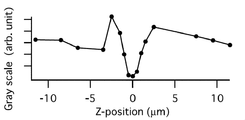
- FIG. 3 is a grayscale plot of the transmission image along the x direction (lateral direction) of the optical information recording medium.
- FIG. 4 is a plot along the Z direction (depth direction) at the in-plane center of the recording pit of the optical information recording medium.
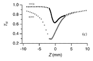
- FIG. 5 is a graph of measurement results of the nonlinear absorption coefficient by the z-scan method.
- examples of the “halogen atom” include a fluorine atom, a chlorine atom, a bromine atom, and an iodine atom.
- the “organic group” means a group containing one or more carbon atoms as its constituent atoms.
- examples of the “organic group” include a hydrocarbon group.
- the “hydrocarbon group” means a group containing one or more carbon atoms and one or more hydrogen atoms as its constituent atoms.
- examples of the “hydrocarbon group” include an aliphatic hydrocarbon group and an aromatic hydrocarbon group (aryl group).
- the “aliphatic hydrocarbon group” may be linear, branched, cyclic, or a combination thereof.
- the “aliphatic hydrocarbon group” may be saturated or unsaturated.
- examples of the “aliphatic hydrocarbon group” include an alkyl group, an alkenyl group, an alkynyl group, and a cycloalkyl group.
- examples of the “alkyl group” include methyl, ethyl, propyl, isopropyl, butyl, isobutyl, sec-butyl, tert-butyl, pentyl, isopentyl, neopentyl, and hexyl. And a linear or branched alkyl group having 1 to 10 carbon atoms.
- alkenyl group examples include vinyl, 1-propenyl, isopropenyl, 2-methyl-1-propenyl, 1-butenyl, 2-butenyl, 3-butenyl, -Ethyl-1-butenyl, 1-pentenyl, 2-pentenyl, 3-pentenyl, 4-pentenyl, 4-methyl-3-pentenyl, 1-hexenyl, 2-hexenyl, 3-hexenyl, 4-hexenyl, and 5- Examples thereof include linear or branched alkenyl groups having 1 to 10 carbon atoms such as hexenyl.
- alkynyl group examples include ethynyl, 1-propynyl, 2-propynyl, 1-butynyl, 2-butynyl, 3-butynyl, 1-pentynyl, 2-pentynyl, Linear or branched alkynyl groups having 2 to 6 carbon atoms, such as 3-pentynyl, 4-pentynyl, 1-hexynyl, 2-hexynyl, 3-hexynyl, 4-hexynyl, and 5-hexynyl Is exemplified.
- examples of the “cycloalkyl group” include cycloalkyl groups having 3 to 8 carbon atoms such as cyclopentyl group, cyclohexyl group, and cycloheptyl.
- alkoxy group is, for example, a group represented by RO— (wherein R is an alkyl group).
- ester group is, for example, a group represented by RCO 2 — (wherein R is an alkyl group).
- the “ether group” means a group having an ether bond (—O—) and includes a polyether group.
- the polyether group has the formula: R a — (O—R b ) n — (wherein R a is an alkyl group, R b is the same or different at each occurrence, is an alkylene group, and n is 1 It is an integer of the above.
- An alkylene group is a divalent group formed by removing one hydrogen atom from the alkyl group.
- the “acyl group” includes an alkanoyl group.
- the “alkanoyl group” is, for example, a group represented by RCO— (wherein R is an alkyl group).
- examples of the “5-membered heteroaryl group” include pyrrolyl (eg, 1-pyrrolyl, 2-pyrrolyl, 3-pyrrolyl), furyl (eg, 2-furyl, 3-pyrrole).
- Furyl thienyl (eg, 2-thienyl, 3-thienyl), pyrazolyl (eg, 1-pyrazolyl, 3-pyrazolyl, 4-pyrazolyl), imidazolyl (eg, 1-imidazolyl, 2-imidazolyl, 4-imidazolyl), Isoxazolyl (eg, 3-isoxazolyl, 4-isoxazolyl, 5-isoxazolyl), oxazolyl (eg, 2-oxazolyl, 4-oxazolyl, 5-oxazolyl), isothiazolyl (eg, 3-isothiazolyl, 4-isothiazolyl, 5-isothiazolyl) , Thiazolyl (eg, 2-thiazolyl, 4-thiazolyl, 5-thiazolyl), triazo (Eg, 1,2,3-triazol-4-yl, 1,2,4-triazol-3-yl), oxadiazolyl (eg, 1,2,4-o
- the “acrylate monomer” includes not only an acrylate having a hydrogen atom at the ⁇ -position but also an acrylate in which the hydrogen atom at the ⁇ -position is substituted with a substituent such as an alkyl group or a halogen atom. To do.
- optical information recording material of the present invention has a specific wavelength in the range of 365 nm to 650 nm. (1) has a non-linear absorption coefficient in the range of 5 to 10,000 cm / GW, and (2) A multilayer diffraction grating is formed.
- the optical information recording material of the present invention has a nonlinear absorption coefficient in the range of 5 to 10000 cm / GW, preferably in the range of 7 to 7000 cm / GW, more preferably in the range of 50 to 6000 cm / GW, still more preferably. It has a non-linear absorption coefficient in the range of 100 to 5000 cm / GW, and even more preferably in the range of 250 to 4000 cm / GW. Since the optical information recording material of the present invention has such a non-linear absorption coefficient, it is possible to form extremely fine recording marks with light of small pulse energy, and stable information recording or reproduction is easy. In addition, recording marks can be formed at high speed (short time).
- a larger pulse energy is advantageous in that a recording mark can be made at a higher speed, but if this is too large, (1) the recording area may be increased, leading to a decrease in information recording density, and (2) If it is too large, the medium may be destroyed undesirably.
- the “nonlinear absorption coefficient” is defined as follows.
- the transmittance T when incident light of light intensity I 0 [W / cm 2 ] passes through a sample with a thickness of L [cm] is based on the Beer-Lambert law. It is expressed.
- I [W / cm 2 ] is the light intensity after passing through the sample
- ⁇ [cm ⁇ 1 ] is the absorption coefficient.
- this absorption coefficient which is normally treated as a constant, depends on the light intensity at the time of actual measurement, it is defined by dividing into a part ⁇ L that does not depend on the light intensity and a dependent part ⁇ NL (I 0 ) as follows.
- ⁇ L is named a linear absorption coefficient
- ⁇ NL (I 0 ) is named a non-linear absorption coefficient.
- ⁇ NL (I 0 ) is not necessarily a constant here (in order to express this explicitly, it is written in the form of a function of I 0 ). That is, ⁇ NL (I 0 ) itself also includes those depending on the incident light intensity I 0 . This definition is phenomenological, and it does not matter in what mechanism the absorption depending on the light intensity appears.
- ⁇ (n) is called the n photon absorption coefficient.
- ⁇ (n) is a two-photon absorption coefficient when n is 2.
- ⁇ (n) is considered as a constant independent of I 0 .
- a multilayer diffraction grating is formed.
- the multilayer diffraction grating formed in the optical information recording material of the present invention preferably has a structure in which a large number of layers having a higher refractive index and layers having a lower refractive index are alternately stacked.
- the difference in refractive index ( ⁇ n) between a layer having a higher refractive index and a layer having a lower refractive index that are adjacent to each other is larger.
- the difference in refractive index ( ⁇ n) is preferably 0.001 or more, more preferably 0.005, more preferably 0.01 or more, and still more preferably 0.02 or more.
- the upper limit is not specifically limited, For example, it can be 0.5.
- the number of diffraction grating layers included in the optical information recording material of the present invention depends on the film thickness of the material layer. For example, when the film thickness of the material layer is 100 ⁇ m, it is preferably 4 or more, more preferably 10 or more, and More preferably, it is 50 or more. Although there is no upper limit to the number of diffraction grating layers included in the optical information recording material of the present invention, the upper limit can usually be 1000 when the thickness of the material layer is 1000 ⁇ m.
- the number of diffraction grating layers of the optical information recording material of the present invention can be confirmed using, for example, a phase difference TEM.
- the direction perpendicular to this layer in other words, the direction parallel to the direction in which the film thickness of the material layer is defined is as follows. This is called the depth direction.
- the number of recording markers that can hold information independent of each other along the depth direction is defined as the number of information recording layers.
- the thickness obtained by dividing the film thickness by the number of information recording layers is the information recording layer thickness, and the information recording layer thickness needs to be at least equal to or greater than the layer thickness of the diffraction grating shown below. .
- the number of information recording layers depends on the thickness of the material layer, for example, when the thickness of the material layer is 100 ⁇ m, it is preferably 4 or more, more preferably 10 or more, and still more preferably 50 or more. Although there is no upper limit to the number of information recording layers of the optical information recording material of the present invention, the upper limit can usually be 1000 when the thickness of the material layer is 1000 ⁇ m.
- the multilayer diffraction grating can be preferably formed by exposure using multilayer optical interference fringes due to optical interference.
- optical interference fringes By using the optical interference fringes, a diffraction grating having an extremely large number of layers can be formed in a short time.
- the optical information recording material of the present invention has a multilayer diffraction grating, so that the optical information recording material of the present invention can extremely reduce the thickness of a single layer of the diffraction grating.
- the thickness of the single layer of the diffraction grating is preferably in the range of 50 to 500 nm, more preferably in the range of 60 to 400 nm, even more preferably in the range of 80 to 300 nm, and even more preferably 100 to 250 nm. Can be within the range of The thickness of the single layer of the diffraction grating can be confirmed using, for example, a phase difference TEM.
- the thickness of the single layer of the diffraction grating is approximate to the wavelength length of the light source irradiated when reading the optical information of the optical information recording material of the present invention, or 1/2 or 1 / of the wavelength of the light source. 4 is desirable.
- the optical information recording material of the present invention is preferably a photosensitive resin and has a wavelength of 365 ⁇ 650 nm at a specific wavelength of 50 ⁇ 10 ⁇ 50 cm 4 ⁇ sec ⁇ molecule ⁇ 1 ⁇ photon ⁇ 1. It contains a nonlinear absorption dye having the above two-photon absorption cross section.
- the two-photon absorption cross section can be determined by the method described in Non-Patent Document 1 or 2, for example.
- the dye may be referred to as a “nonlinear absorbing dye”.
- Non-Patent Document 1 Kenji Kamada, “Evaluation Method of Two-Photon Absorbing Materials”, “Development and Application of Highly Efficient Two-Photon Absorbing Materials”, Toshiyuki Watanabe, Chapter 2, CMC Publishing, 2011, pp.16-27.
- Non-Patent Document 2 M. Sheik-Bahae, AA Said, TH Wei, DJ Hagan, EW Van Stryland, IEEE J. Quant. Electron., 1990, 26, 760-769.
- the optical information recording material of the present invention is preferably an optical information recording material produced by a production method including the following steps (1), (2), and (3), or a production method according thereto, for example. be able to. That is, the optical information recording material and the composition for optical information recording material of the present invention can each contain a compound described in the following production method or a compound derived therefrom.
- the optical information recording material of the present invention includes the compositions of the following examples.
- Example 1-2 Diol compounds, An alicyclic epoxy group-containing cationic polymerizable compound, Fluorine-free radically polymerizable compound, Optional cationic polymerization catalyst, A composition containing a non-linear absorbing dye and an optional photopolymerization initiator and / or a compound derived therefrom.
- Example 2-1 Diol compounds, An alicyclic epoxy group-containing cationic polymerizable compound, Fluorine-containing radically polymerizable compound, Optional cationic polymerization catalyst, A composition comprising a nonlinear absorbing dye and an optional photoinitiator.
- Example 2-2 Diol compounds, An alicyclic epoxy group-containing cationic polymerizable compound, Fluorine-containing radically polymerizable compound, Optional cationic polymerization catalyst, A composition containing a non-linear absorbing dye and an optional photopolymerization initiator and / or a compound derived therefrom.
- composition of the present invention is: A nonlinear absorption dye having a two-photon absorption cross-section of 50 ⁇ 10 ⁇ 50 cm 4 ⁇ sec ⁇ molecule ⁇ 1 ⁇ photon ⁇ 1 or more at a specific wavelength in the range of 365 nm to 650 nm; Diol compounds, It is a composition containing an alicyclic epoxy group-containing cationically polymerizable compound and a fluorine-containing radically polymerizable compound.
- the fluorine-containing radical polymerizable compound can be preferably a fluorine-containing acrylate monomer. Since the fluorine-containing radical polymerizable compound has a low refractive index, it is possible to reduce the noise of the reproduction signal by increasing the refractive index difference of the diffraction grating during the initialization.
- Suitable examples of the preparation of the composition for optical information recording material of the present invention include the following preparation method examples.
- Preparation method example 1 Diol compounds, An alicyclic epoxy group-containing cationic polymerizable compound, Fluorine-free radically polymerizable compound, A preparation method comprising a step of mixing a cationic polymerization catalyst, a non-linear absorbing dye, and a photopolymerization initiator.
- Preparation method example 2 Diol compounds, An alicyclic epoxy group-containing cationic polymerizable compound, Fluorine-containing radically polymerizable compound, A preparation method comprising a step of mixing a cationic polymerization catalyst, a non-linear absorbing dye, and a photopolymerization initiator.
- the method of Preparation Method Example 2) can be suitably employed.
- Examples of the “diol compound” are those represented by the formula: HO— (CH 2 ) a1 — ((CH 2 ) b —O) c— (CH 2 ) a2 —OH, wherein a1 and a2 are the same or different Represents 0, 1, or 2, b represents 1 to 10, and c represents a number of 1 to 100. ] The compound represented by this is included.
- Monohydric alcohols such as ethylene glycol monomethyl ether, ethylene glycol monobutyl ether, diethylene glycol monomethyl ether, dipropylene glycol monobutyl ether and their alkylene oxide adducts; and ethylene glycol, diethylene glycol, propylene glycol, dipropylene glycol, 1,2- Butanediol, 1,3-butanediol, 1,4-butanediol, 1,5-pentanediol, neopentyl glycol, isoprene glycol (3-methyl-1,3-butanediol), 1,2-hexanediol, 1,6-hexanediol, 3-methyl-1,5-pentanediol, 1,2-octanediol, octanediol (2-ethyl-1,3-hexanediol) 2-butyl-2-ethyl-1,3
- the “alicyclic epoxy group-containing cationic polymerizable compound” is, for example, a compound containing an epoxy group-containing cycloalkyl group.
- the “alicyclic epoxy group-containing cationic polymerizable compound” can be a polyfunctional epoxy compound having two or more epoxy groups. Examples of the alicyclic epoxy resin include 3,4,3 ′, 4′-diepoxybicyclohexyl, bis (3,4-epoxycyclohexyl) adipate, and the like.
- Examples of the “polyfunctional epoxy compound” include the following formula (1): (In the formula, r represents a number from 0 to 10.) The compound represented by these is included. Here, the compound may be a mixture (eg, equivalent mixture) of a compound in which r is 0 and a compound in which r is a number of 1 to 10.
- Examples of the “polyfunctional epoxy compound” also include the following compounds.
- the fluorine-free radically polymerizable compound is a compound having a radically polymerizable group.
- a preferred radical polymerizable group is represented by the following formula: [Wherein R b is a single bond, —O—, —CO— or —OC (O) —; R c represents a hydrogen atom, an alkyl group having 1 to 10 carbon atoms (preferably an alkyl group having 1 to 3 carbon atoms, more preferably a methyl group), a lactam group (preferably ⁇ -lactam, ⁇ -lactam or ⁇ A -lactam group, more preferably a ⁇ -lactam group) or a phenyl group, preferably a methyl group or a hydrogen atom.
- More preferred radical polymerizable groups have the following formula: [Wherein R c has the same meaning as described above. ] It is group represented by these.
- a more preferred radical polymerizable group is an acryloyl group or a methacryloyl group.
- Suitable examples of the fluorine-free radically polymerizable compound in the present invention include an acrylate monomer and an acrylic copolymer having a structural unit derived therefrom.
- fluorine-free radical polymerizable compound examples include Styrene, ⁇ -methylstyrene, 2-bromostyrene, vinyl acetate, methyl vinyl ketone, acrylonitrile, N-vinyl carbazole, N-vinyl pyrrolidone, acrylate, methyl acrylate, n-butyl acrylate, lauryl acrylate, 2-ethylhexyl acrylate, dicyclopentanyl acrylate, phenyl acrylate , O-biphenyl acrylate, 2-naphthyl acrylate, ethylene oxide phenol acrylate, phenoxydiethylene glycol acrylate, phenoxy-polyethylene glycol acrylate, nonylphenol ethylene oxide acrylate, bisphenol A ethylene oxide diacrylate, ethylene oxide tetrabromobisphenol A diacrylate, ethylene oxide bisphenol A diacrylate , Propylene oxide bisphenol A diacrylate, propylene oxide
- 9,9-bis (4-acryloxydipropoxyphenyl) fluorene 9,9-bis (4-acryloxyethoxy-3,5-dimethyl) fluorene, 9,9-bis (4-acryloxytriethoxyphenyl) fluorene, 9,9-bis (4-acryloxyethoxy-3-methylphenyl) fluorene
- Examples include 9,9-bis (4-acryloxyethoxy-3-ethylphenyl) fluorene and 9,9-bis (4-acryloxydiethoxyphenyl) fluorene.
- Examples of the “fluorine-free radical polymerizable compound” are further diallyl phthalate monomers, and Is mentioned.
- Examples of the “fluorine-free radical polymerizable compound” further include 2,4-bis ( ⁇ -acryloyloxyethylthio) diphenyl ketone, 4,4′-bis ( ⁇ -acryloyloxyethylthio) diphenyl ketone, 4,4′-bis ( ⁇ -acryloyloxyethylthio) diphenyl ketone, tri (acryloyloxyethyl) isocyanurate, acrylamide, methylenebisacrylamide, diacetone acrylamide, cyclohexene oxide, ethoxylated propylene glycol 700 diacrylate, propoxylated ethoxy Diacrylate, dendrimer (2nd generation) acrylate, and compounds obtained by replacing acrylate with methacrylate.
- fluorine-free radically polymerizable compound examples are not limited to those exemplified above, but 9,9-bis (4-acryloxydipropoxyphenyl) from the viewpoint of recording sensitivity and multiple recording properties.
- Fluorene, diallyl phthalate monomer, propoxylated ethoxylated bisphenol A diacrylate, polypropylene glycol 700 diacrylate, those having an ⁇ -fluoroacryloyl group or acryloyl group, and compounds in which the acrylate is replaced with methacrylate are preferred.
- the fluorine-containing radical polymerizable compound is a compound having a radical polymerizable group.
- a preferred radical polymerizable group is represented by the following formula: [Wherein R b is a single bond, —O—, —CO— or —OC (O) —; R c represents a hydrogen atom, a fluorine atom, or an alkyl group having 1 to 10 carbon atoms (preferably an alkyl group having 1 to 3 carbon atoms, more preferably a methyl group) optionally substituted by a fluorine atom, a lactam group (Preferably ⁇ -lactam, ⁇ -lactam or ⁇ -lactam group, more preferably ⁇ -lactam group) or a phenyl group, preferably a methyl group or a hydrogen atom.
- More preferred radical polymerizable groups have the following formula: [Wherein R c has the same meaning as described above. ] It is group represented by these.
- a more preferred radical polymerizable group is an acryloyl group or a methacryloyl group.
- Suitable examples of the fluorine-containing radical polymerizable compound in the present invention include an acrylate monomer having a fluorine-containing group, and an acrylic copolymer having a structural unit derived therefrom.
- Examples of the acrylate monomer having a fluorine-containing group include a formula (4): [Wherein, X represents a hydrogen atom, a methyl group, a fluorine atom, a chlorine atom, a bromine atom, an iodine atom, a CFX 1 X 2 group (where X 1 and X 2 represent a hydrogen atom, a fluorine atom, a chlorine atom, bromine A cyano group, a linear or branched fluoroalkyl group having 1 to 21 carbon atoms, a substituted or unsubstituted benzyl group, a substituted or unsubstituted phenyl group, Y represents a direct bond, an aliphatic group having 1 to 10 carbon atoms which may have an oxygen atom, an aromatic group having 6 to 10 carbon atoms which may have an oxygen atom, a cyclic aliphatic group or an aromatic group.
- R 1 represents an alkyl group having 1 to 4 carbon atoms
- Y 1 is a hydrogen atom or an acetyl group
- Rf represents a linear or branched fluoroalkyl group having 1 to 7 carbon atoms, a fluoroalkenyl group having 2 to 7 carbon atoms, or repeating units: —C 3 F 6 O—, —C 2 F 4 O— and —
- a fluoroether group having a total number of 1 to 200 of at least one repeating unit selected from the group consisting of CF 2 O—.
- Indicated by X is preferably a hydrogen atom or a methyl group.
- Rf group when the Rf group is a fluoroalkyl group, it is preferably a perfluoroalkyl group.
- Rf groups include —CF 3 , —CF 2 CF 3 , —CF 2 CF 2 CF 3 , —CF (CF 3 ) 2 , —CF 2 CF 2 CF 2 CF 3 , —CF 2 CF (CF 3 ) 2 , —C (CF 3 ) 3 , — (CF 2 ) 4 CF 3 , — (CF 2 ) 2 CF (CF 3 ) 2 , —CF 2 C (CF 3 ) 3 , —CF (CF 3 ) CF 2 CF 2 CF 3 , — (CF 2 ) 5 CF 3 , — (CF 2 ) 3 CF (CF 3 ) 2 , — (CF 2 ) 4 CF (CF 3 ) 2 , — (CF 2 ) 2 H, — CF 2 CFHCF 3 ,
- the number of carbons in the Rf group should be 1 to 7, for example 2 to 6, especially 4 to 6, especially 6 from the viewpoints of PFOA and functions described above. Is preferred.
- the Rf group is a fluoroalkenyl group, it is preferably a perfluoroalkenyl group.
- the Rf group is a fluoroalkenyl group
- the Rf group preferably has 2 to 7 carbon atoms, particularly 3 to 6 carbon atoms, especially 6 carbon atoms.
- the fluoroether group is at least one repeating unit selected from the group consisting of —C 3 F 6 O—, —C 2 F 4 O—, and —CF 2 O— (oxypar group). Fluoroalkylene group).
- —C 3 F 6 O— is —CF 2 CF 2 CF 2 O— or —CF 2 C (CF 3 ) FO—.
- —C 2 F 4 O— is generally —CF 2 CF 2 O—.
- the total number of oxyperfluoroalkylene repeating units is 1 to 200, for example 1 to 100, in particular 5 to 50.
- the fluoroether group has a terminal group that is directly bonded to the oxyperfluoroalkylene repeat unit.
- the terminal group are a hydrogen atom, a halogen atom (eg, a fluorine atom), an alcohol group (eg, HOCH 2 —), an amine group (eg, H 2 N—), and a chloromethyl group (ClH 2 C—).
- the fluoroether group may have a C1-C10 fluoroalkylene group, particularly a perfluoroalkylene group, in addition to the oxyperfluoroalkylene repeating unit and the terminal group.
- Examples of the fluoroalkylene group having 1 to 10 carbon atoms are —CF 2 — and —CF 2 CF 2 —.
- fluoroether groups that are examples of Rf groups are as follows.
- F- (CF 2 CF 2 CF 2 O) n -CF 2 CF 2- (n is 1 to 200)
- F- (CF 2 C (CF 3 ) FO) n -CF 2 CF 2- (n is 1 to 200)
- F- (CF 2 C (CF 3 ) FO) n- (CF 2 O) m -CF 2 CF 2- (total of n and m is 1 to 200)
- F- (CF 2 CF 2 O) n- (CF 2 O) m -CF 2 CF 2- total of n and m is 1 to 200)
- Y represents a direct bond, an aliphatic group having 1 to 10 carbon atoms which may have an oxygen atom, an aromatic group having 6 to 10 carbon atoms which may have an oxygen atom, a cyclic aliphatic group or an aromatic group.
- the aliphatic group is preferably an alkylene group (particularly having 1 to 4 carbon atoms, such as 1 or 2).
- the aromatic group, cycloaliphatic group and araliphatic group may be either substituted or unsubstituted.
- Examples of the acrylate monomer having a fluorine-containing group are as follows.
- 2 OCOCH CH 2 Rf-SO 2 N (C 2 H 5)
- Rf is a linear or branched fluoroalkyl group having 1 to 7 carbon atoms, a fluoroalkenyl group having 2 to 7 carbon atoms, or a repeating unit: —C 3 F 6 O—, —C 2 F 4 A fluoroether group having a total number of 1 to 200 of at least one repeating unit selected from the group consisting of O— and —CF 2 O—.
- Examples of the cationic polymerization catalyst include aromatic diazonium salts, aromatic iodonium salts, aromatic sulfonium salts, aromatic phosphonium salts, mixed ligand metal salts, and aromatic onium salts.
- aromatic diazonium salts aromatic diazonium salts
- aromatic iodonium salts aromatic iodonium salts
- aromatic sulfonium salts aromatic phosphonium salts
- mixed ligand metal salts and aromatic onium salts.
- aromatic onium salts for example, Sun-Aid SI-60L, 80L, 110L (all manufactured by Sanshin Chemical Industry Co., Ltd .: trade name) can be used.
- the two-photon absorption cross-section of the “nonlinear absorption dye” used in the present invention has a specific wavelength in the range of 365 nm to 650 nm.
- the optical information recording medium of the present invention is based on the fact that the nonlinear fringe dye is contained, and by irradiating the pulsed light laser, the interference fringes are locally destroyed at high speed (short time), whereby the recording mark is recorded. Can be formed.
- the “nonlinear absorption dye” used in the present invention is preferably a hydrocarbon having two or more benzene rings, which may have one or more substituents, based on nonlinear absorption.
- a condensed aromatic hydrocarbon which may have one or more substituents.
- Preferred examples of the “hydrocarbon” include naphthalene, anthracene, phenanthrene, 1,4-bis (phenylethynyl) benzene, and pyrene.
- the “substituent” include a halogen atom, a hydroxy group, and an organic group.
- the “photosensitizer” used in the present invention is not particularly limited as long as it is based on light interference fringes and can sensitize a photopolymerization initiator, and known ones can be used.
- thiopyrylium salt compounds, merocyanine compounds, quinoline compounds, styrylquinoline compounds, coumarin compounds, ketocoumarin compounds, thioxanthene compounds, xanthene compounds, oxonol compounds, cyanine compounds, rhodamine compounds, pyrylium examples thereof include salt compounds.
- the photosensitizer is preferably colorless and transparent by being decomposed by a post-process after hologram recording, heating or ultraviolet irradiation.
- a photosensitizer can be used individually or in combination of 2 or more types.
- a styryl compound or a coumarin compound is preferable, and specifically, 2- (p-dimethylaminostyryl) quinoline, 2- (p-diethylaminostyryl) quinoline, 4- (p-dimethylaminostyryl) quinoline.
- coumarin compounds 7-diethylamino-4-methylcoumarin, 7-ethylamino-4-trifluoromethylcoumarin, 4,6-diethylamino-7-ethylaminocoumarin, 3- (2-benzimidazolyl)- 7-N, N-diethylaminocoumarin, 7-diethylaminocyclopenta (c) coumarin, 7-amino-4-trifluoromethylcoumarin, 1,2,3,4,5,3H, 6H, 10H-tetrahydro-8- Trifluoromethyl (1) benzopyrano- (9,9A, 1-gh) -quinolizin-10-one, 7-ethylamino-6-methyl-4-trifluoromethylcoumarin, 1,2,3,4,5, 3H, 6H, 10H-Tetrahydro-9-carbethoxy (1) benzopyrano (9,9a, 1-gh) -quinolidine-10 On and the like.
- the photopolymerization initiator is not particularly limited as long as it is a compound that activates photoradical polymerization.
- peroxide esters such as t-butylperoxybenzoate; t-butylhydroperoxide, di-t- Peroxides such as butyl peroxide; benzoin / benzoin alkyl ethers such as benzoin, benzoin methyl ether, benzoin ethyl ether, benzoin isopropyl ether; acetophenone, 2,2-dimethoxy-2-phenylacetophenone, 2,2-diethoxy- 2-phenylacetophenone, 1,1-dichloroacetophenone, 2-methyl-1- [4- (methylthio) phenyl] -2-morpholino-propan-1-one, 2-benzyl-2-dimethylamino-1- (4 -Morpholinophenyl)- Acetophenones such as tan-1-one; anthraquino
- composition for optical information recording materials of the present invention may contain other components.
- An example of another component is a plasticizer.
- plasticizers include phthalates represented by dimethyl terephthalate, diethyl terephthalate, dimethyl phthalate, and dioctyl phthalate; dimethyl adipate, diethyl adipate, dibutyl adipate, dimethyl sebacate, diethyl sebacate, dibutyl sebacate Aliphatic dibasic esters represented by Kate and diethyl succinate; orthophosphates represented by trimethyl phosphate, triethyl phosphate, triphenyl phosphate and tricresyl phosphate; typified by glyceryl triacetate and 2-ethylhexyl acetate Acetic acid esters; inactive compounds such as phosphites represented by triphenyl phosphite and
- Step (2) The curing and curing of the epoxy group-containing cationic polymerizable substance of the composition may be carried out by employing a method according to the type of the epoxy group-containing cationic polymerizable substance.
- an epoxy group-containing cationic polymerizable material is cured by a cationic polymerization catalyst. Curing in the case of a thermal cationic polymerization catalyst can be performed by heating at an appropriate time and temperature condition.
- Step (2) is, for example, a step in which the composition is applied on a base material, and the alicyclic epoxy group-containing cationic polymerizable substance is cationically polymerized and cured by heating.
- Step (3) Formation of Diffraction Grating
- the diffraction grating is preferably formed over the entire cured product to be the optical information recording region. In this specification, this is also called initialization.
- the diffraction grating layer of the optical information recording medium of the present invention is formed by optical interference exposure using two lights having coherence with each other.
- the angle formed by the two lights forming the diffraction grating, that is, the crossing angle is 90 ° to 270 ° with respect to each other in the definition that the angle formed when both are parallel and the traveling direction of the wavefront is the same direction is 0 °.
- Is in the range preferably in the range of 135 ° to 225 °, more preferably in the range of 170 ° to 190 °.
- Appropriate conditions can be adopted as the light irradiation conditions depending on the substance contained in the optical information recording material.
- the wavelength is in the range of 400 to 650 nm, and the range of 1 to 1000 mW / cm 2 .
- a layer of interference fringes can be formed.
- the number of layers of the diffraction grating can be adjusted by the film thickness and the crossing angle of the optical information recording material.
- the optical information recording material of the present invention has a wavelength in the range of 365 nm to 650 nm from the viewpoint that the optical information recording material can easily form a recording mark over the entire optical information recording material by the operation of step (4) described later.
- it has a visible light transmittance of 50% or more, more preferably 60%, and even more preferably 70%.
- the value of visible light transmittance is determined by the measurement method described in JIS K 7375: 2008.
- the shape of the optical information recording material is not particularly limited, but may be, for example, a flat plate shape.
- the “multilayer diffraction grating” or the “multilayer interference fringes” can be arranged in parallel to the planar direction of the flat plate.
- the thickness is usually in the range of 50 to 600 ⁇ m.
- the recording marks can be formed by locally destroying the multilayer interference fringes formed in the step (3).
- This optical information recording material is initialized by the operation in the step (3), so that when the reading light is irradiated when reproducing information, the reproduction light returns from the medium, but the recording is performed by the operation in the step (4). Since the reproduction light does not return when the mark is formed, it is possible to recognize which value “0” or “1” is recorded as information.
- the optical information recording medium of the present invention is In the specific wavelength containing the optical information recording material of the present invention described above and having a wavelength in the range of 365 nm to 650 nm, It has a visible light transmittance of 50% or more.
- the number of layers of the optical information recording medium of the present invention depends on the thickness of the material layer, for example, when the thickness of the material layer is 100 ⁇ m, it is preferably 4 or more, more preferably 10 or more, and still more preferably. 50 or more.
- the optical information recording medium of the present invention usually has a recording layer comprising the optical information recording material of the present invention, and a base material layer,
- a recording layer comprising the optical information recording material of the present invention
- a base material layer for example, one aspect of the optical information recording medium of the present invention has a structure in which a recording layer is sandwiched between two base material layers together with a spacer. That is, the thickness of the recording layer is determined by the thickness of the spacer.
- Examples of the material of the base material layer used in the optical information recording medium of the present invention include glass, polycarbonate, polymethyl methacrylate, cycloolefin polymer and the like.
- the spacer used in the optical information recording medium of the present invention is not particularly limited as long as the thickness is uniform, and examples of the material include metals, ceramics, resins, and the like.
- examples of the material of the base material layer on the side irradiated with light among the two base material layers include glass.
- examples of the material of the other substrate layer of the two substrate layers include polycarbonate.
- the thickness of the recording layer is usually in the range of 50 to 1000 ⁇ m.
- the thickness of each base material layer is usually in the range of 50 to 1100 ⁇ m.
- the thickness of the optical information recording medium is usually in the range of 150 to 1200 ⁇ m.
- the absorption coefficient at 405 nm of the recording layer is preferably 150 cm ⁇ 1 or less, more preferably 100 cm ⁇ 1 or less, and further preferably 50 cm ⁇ 1 or less.
- the transmittance of the base material layer at 405 nm is preferably 50% or more, more preferably 90% or more, and still more preferably 95% or more.
- a recording mark having a diameter (major axis) of preferably 0.8 ⁇ m or less, more preferably 0.5 ⁇ m or less, and further preferably 0.4 ⁇ m or less can be formed.
- the diameter (major axis) is preferably small and the lower limit thereof is not limited, but in the present invention, the lower limit is, for example, 0.1 ⁇ m.
- recording marks can be formed at a recording speed (recording time) of preferably 50 nanoseconds (ns) or less, more preferably 30 ns or less, and even more preferably 8 ns or less.
- the recording speed (recording time) is preferably short, and the lower limit thereof is not limited, but in the present invention, the lower limit is, for example, 1 ns.
- the recording time can be determined by forming the recording mark by one-time laser irradiation for the set pulse width in the pulse laser used for forming the recording mark.
- the S / N ratio after formation of the recording mark is determined from the ratio between the base count value and the peak value of the initialized medium, preferably 1.0 or more, more preferably 2. It can be 0 or more, more preferably 2.5 or more.
- the S / N ratio is preferably large and the upper limit is not limited, but in the present invention, the upper limit is 10, for example.
- the optical information recording medium of the present invention can be understood from the production of the material of the present invention described above. That is, the optical information recording medium of the present invention is, for example, (1) The liquid of the composition constituting the optical information recording material of the present invention described above is applied to a substrate (for example, one of the base material layers), (2) The liquid can be cured, and (3) optical interference fringes can be formed over the entire cured product to be an optical information recording area. Curing may be performed by employing a method according to the type of the polymerizable substance. For example, when the polymerizable substance is a thermosetting substance, the curing can be performed by heating at an appropriate time and temperature condition.
- the diffraction grating layer of the optical information recording medium of the present invention is formed by light irradiation by the two-beam interference method.
- the conditions of light irradiation by the two-beam interference method can be appropriately selected according to the substance contained in the optical information recording material.
- the wavelength is in the range of 365 to 650 nm, and 1 to 1000 mW / cm.
- the layer of the diffraction grating can be formed by irradiation with light having an intensity in the range of 2 and for a time in the range of 0.1 to 2000. At this time, the reflected light from the surface of the optical information recording material layer or the base material becomes an obstacle for reading a signal from the reproduction light overlapping with the reproduction light, and acts as noise.
- the incident angle of the incident light has an inclination of about 5 ° to 15 ° with respect to the normal line.
- the number of interference fringe layers can be adjusted by the film thickness of the optical information recording material and the angle formed by the two light beams.
- the thickness of the interference fringe layer can be adjusted by the spacer of the optical information recording material.
- the present invention also provides the following inventions.
- (1) has a non-linear absorption coefficient in the range of 5 to 10,000 cm / GW, and (2) A non-linear absorption dye used in an optical information recording material in which a multilayer diffraction grating is formed, Non-linear absorption dye having a two-photon absorption cross section of 100 ⁇ 10 ⁇ 50 cm 4 ⁇ sec ⁇ molecule ⁇ 1 ⁇ photon ⁇ 1 or more.
- the nonlinear absorption type optical information recording apparatus of the present invention (1) (a) a laser that generates pulsed laser light having a pulse width in the range of 0.1 to 30 nanoseconds, (b) a wavelength in the range of 365 to 650 nm, and (c) a peak output of 1000 W or less Generator, (2) a laser condensing device comprising an objective lens having (a) a numerical aperture in the range of 0.5 to 1.0, and (b) a magnification in the range of 1 to 100 times, (3) (a) the optical information recording material of the present invention, or (b) a storage device for storing the optical information recording medium of the present invention, and (4) A mechanism for scanning a predetermined condensing position in the optical information recording material or the optical information recording medium with a laser beam is provided.
- the laser generator included in the nonlinear absorption type optical information recording apparatus of the present invention comprises (1) (a) a pulse width in the range of 0.1 to 30 nanoseconds, and (b) in the range of 365 to 650 nm. Any pulse laser beam having a wavelength and (c) a peak output of 1000 W or less may be generated, and other pulse laser beam may be generated.
- the wavelength is preferably in the range of 400 to 650 nm, more preferably in the range of 400 to 532 nm, and even more preferably in the range of 400 to 410 nm.
- the peak output is preferably 150 W or less, more preferably 120 W or less.
- the numerical aperture is preferably 0.5 or more, more preferably 0.7 or more, and still more preferably 0.8 or more.
- the wavelength is in the range of 400 to 532 nm, the peak power is 150 W or less, and the numerical aperture is 0.5 or more; More preferably, the wavelength is in the range of 400-410 nm, the peak power is 150 W or less, and the numerical aperture is 0.7 or more; and more preferably The wavelength is in the range of 400 to 410 nm, the peak output is 120 W or less, and the numerical aperture is 0.8 or more.
- FIG. 1 is a sectional view showing an outline of an example of an optical information recording medium of the present invention.
- FIG. 2 is a schematic diagram showing an outline of an example of the nonlinear absorption type optical information recording apparatus of the present invention.
- the optical information recording apparatus comprises: (a) a pulse laser beam having a pulse width in the range of 0.1 to 30 nanoseconds, (b) a wavelength in the range of 365 to 650 nm, and (c) a peak output of 1000 W or less.
- Laser generating device a laser condensing device comprising an objective lens having (a) a numerical aperture in the range of 0.5 to 1.0, and (b) a magnification in the range of 1 to 100 times
- the optical information recording material of the present invention or an optical information recording medium accommodating device capable of accommodating the optical information recording medium, and a mechanism for scanning a predetermined condensing position of the optical information recording medium with a laser beam
- the optical information recording medium contains a non-linear absorption dye having a two-photon absorption cross-section of 50 ⁇ 10 ⁇ 50 cm 4 ⁇ sec ⁇ molecule ⁇ 1 ⁇ photon ⁇ 1 or more.
- the recording arm unit 100 includes a neutral density filter 6, a first beam expander 7, and a first mirror 8.
- the read arm unit 200 includes a continuous wave laser diode 12, a second beam expander 14, and a second mirror 15.
- the optical readout unit 300 includes a first beam splitter 9 and a second beam splitter 16, a CCD camera 18, a fiber connection port 20, and a spectrometer 19.
- the optical information recording medium 1 is composed of two antireflective coating glasses 2 and a photocrosslinkable resin doped with a non-linear absorbing dye sandwiched between them (this includes an optical information recording layer 3 which is an optical information recording region). To make up. Before optical information recording, a diffraction grating is formed inside the optical information recording medium 1 by interference exposure.
- the diffraction grating is formed by making the interference light incident on the entire optical information recording layer 3.
- the incident angle of the interference light is about 5 ° to 15 ° with respect to the normal line
- the reading light is incident on the medium along the normal line
- the incident light enters the optical information recording layer.
- the reproduction light returning from the formed diffraction grating is emitted from the same normal by the same angle, that is, in this case with an inclination of about 5 ° to 15 °, so that the optical information recording that returns along the normal is recorded. It is possible to make an angle difference from the reflected light from the surface of the medium, and it is possible to avoid the reflected light acting as noise on the reproduction light.
- the optical information recording medium 1 on which the diffraction grating is formed is also referred to as “initialization medium”.
- the pulse laser beam 5 generated from the laser generator 4 passes through the neutral density filter 6 and the first beam expander 7 and is redirected by the first mirror 8 and the first beam.
- the direction is further changed by the splitter 9, and the reflected light is condensed by a laser condensing device including an objective lens 10 and irradiated onto the optical information recording layer 3 inside the recording medium 1.
- the optical information recording medium 1 is accommodated in an accommodation device including a power stage 11.
- the pulsed laser beam is focused by the objective lens 10, is focused in the optical information recording layer 3 of the optical information recording medium 1, becomes high light intensity, and induces nonlinear absorption of the nonlinear absorbing dye. .
- the diffraction grating of the optical information recording layer 3 is locally destroyed by the thermal energy generated by this nonlinear absorption.
- the focal point of the pulse laser beam 5 in the optical information recording layer 3 can be moved by moving the optical information recording medium 1 by the power stage 11. By repeatedly performing the condensing operation controlled in this way, the diffraction grating can be locally broken at an arbitrary position in three dimensions. Thus, three-dimensional recording of information becomes possible.
- the output beam 13 of the continuous wave laser diode 12 passes through the second beam expander 14 and is directed by the second mirror 15 and the first beam splitter 9 used only for reading. And is passed through the second beam splitter 16 and introduced into the optical readout unit 300.
- the reflected reproduction light is not detected at the locally destroyed portion, whereas the reproduced light is detected at the non-destructed portion. Is done.
- the recording conditions and reading conditions employed in the following examples and the like are as follows. ⁇ Recording and reading conditions> Objective lens: 50x, numerical aperture (NA) 0.80 Recording light: Pulse energy 600 to 1000 nJ / pulse, center wavelength 401 nm, full width at half maximum of 5 nm, pulse width 8 ns, recording peak power 75 to 125 W, pulse repetition frequency 1 kHz Reading light: optical power 2.1 ⁇ W, central wavelength 408 nm, full width at half maximum of 3 nm, continuous light
- the recording peak power and the optical power of the reading light are values between the objective lens 10 and the recording medium 1. is there.
- the recording mark size and the S / N ratio were measured by the following methods, respectively.
- the recorded major axis was determined as the full width at half maximum of the change in the gray scale value of the image of the recording mark taken by the optical microscope.
- Example 1 [(1) Preparation of photosensitive solution] With respect to 17.0 parts by weight of an acrylic fluorene monomer having the following chemical formula, which is a fluorine-free radically polymerizable substance having an acrylate group, [Wherein, p and q are 0 to 3.
- the optical information recording medium is initialized by forming a diffraction grating by performing interference exposure by the two-beam interference method over the entire optical information recording area in advance before recording the optical information on the optical information recording medium. It was.
- the conditions at that time were a light source wavelength of 405 nm, a light intensity of 7 mW / cm 2 , and an initialization time of 20 s. At this time, the incident angle of the interference light was inclined by about 5 ° to 15 ° with respect to the normal line.
- the optical information recording / reproducing apparatus locally collects the 8 ns pulsed light described in the ⁇ Recording / Reading Conditions> from the nanosecond pulse laser as the light source at the site where information is recorded. By doing so, the diffraction grating containing the nonlinear absorption dye in the recording region was locally destroyed. At this time, the region where one piece of information was recorded was performed under the condition that only one relevant pulse was irradiated. This condition was performed by sufficiently moving the optical information recording medium in the direction perpendicular to the incident direction of the recording light between the irradiation of a certain light pulse and the irradiation of the next light pulse.
- “sufficient” means an amount of movement in which the recording marker formed by the preceding light pulse does not cause a spatial overlap with the recording marker formed by the light pulse that follows in time.
- the recorded marker size is 0.7 ⁇ m in full width at half maximum, and the time interval between the light pulse and the next light pulse is 1 because the repetition frequency of the pulse light used is 1 kHz. ms, and the moving speed of the optical information recording medium was 6 ⁇ m per 1 ms, so that the recording markers did not sufficiently overlap each other.
- transmission images of the optical information recording medium at different focal positions ie different depths) were acquired [recording peak output set to 71 W (threshold output)].
- the lateral size of the pit was 0.7 ⁇ m in full width at half maximum.
- FIG. 4 shows a plot along the Z direction (depth direction) at the in-plane center of the recording pit, as in FIG.
- the depth dimension of the pit was 2.4 ⁇ m in full width at half maximum.
- the optical information recording / reproducing apparatus having this negative type micro-reflector can reproduce the information from the part where the reproduction light returns from the hologram when the reading light is irradiated and the hologram interference fringes are locally destroyed.
- the S / N according to the definition in reading information was 2.5 or more.
- the recording of information due to the destruction of the diffraction grating at the recording site is formed by irradiation with a single pulse having a duration of 8 ns.
- Non-Patent Document 3 ITE Technical Vol.35, No.27 MMS2011-17 (Jul. 2011).
- the nonlinear absorption coefficient was measured by the z-scan method described in Non-Patent Documents 1 and 2 for the information recording medium that was not recorded, the result of measuring the measurement time was that the scan direction was changed twice.
- FIG. 5 shows the result of scanning with an 8 ns pulse and an excitation wavelength of 402 nm.
- the upper dot indicates a forward scan
- the lower dot indicates a return scan.
- the recording capacity was estimated to be about 80 GB with a thickness of 100 ⁇ m and 20 recording layers.
- the optical recording capacity exceeding the TB class can be improved to 10 TB recording capacity with a recording layer of 40 ⁇ m thickness and 800 ⁇ m by optimizing the optical equipment.
- BPEB 1,4-bis (phenylethynyl) benzene
- “Diol compounds (as soft segments)” include PTG, polyethylene glycol (hereinafter sometimes referred to as PEG), polypropylene glycol (hereinafter sometimes referred to as PPG), and polytetramethylene glycol (hereinafter referred to as PPG).
- An optical information recording medium was prepared by adding PTMG).
- PEG polyethylene glycol
- PPG polypropylene glycol
- PPG polytetramethylene glycol
- Optical information recording medium 2 Antireflection agent coated glass 3: Optical information recording layer 4: Laser generator 5: Pulse laser beam 6: Neutral filter 7: First beam expander 8: First mirror 9: First Beam splitter 10: Objective lens 11: Power stage 12: Continuous oscillation laser diode 13: Output beam 14: Second beam expander 15: Second mirror 16: Second beam splitter 17: Third beam splitter 18: CCD camera 19 : Spectrometer 20: Fiber connection port 100: Recording arm unit 200: Reading arm unit 300: Optical reading unit
Landscapes
- Physics & Mathematics (AREA)
- Optics & Photonics (AREA)
- Engineering & Computer Science (AREA)
- Manufacturing & Machinery (AREA)
- General Physics & Mathematics (AREA)
- Optical Record Carriers And Manufacture Thereof (AREA)
- Optical Recording Or Reproduction (AREA)
- Manufacturing Optical Record Carriers (AREA)
- Diffracting Gratings Or Hologram Optical Elements (AREA)
Abstract
本発明の課題は、小さなパルスエネルギーの光によって、極めて微細な記録マークの形成が可能であり、安定した情報の記録又は再生が容易であり、かつ高速(短時間)での記録マークの形成な光情報記録媒体等を提供することにある 前記課題は、 波長が365nm~650nmの範囲にある特定の波長において、 (1)5~10000cm/GWの範囲内の非線形吸収係数を有し、且つ (2)多層の回折格子が形成されている 光情記録材料 によって解決される。
Description
本発明は、情報記録材料、及び媒体とその記録方法に関する。
従来、光情報記録媒体としては、CD(Compact Disc)、DVD(Digital Versatile Disc)、及びBlu-ray Disc(登録商標、以下BDと称する場合がある。)等の円盤状の光ディスクが普及している。
近年、このような光情報記録媒体には、大容量化が求められ、実際に、極めて大量のデータの記録が可能になっているが、さらなる大容量化が求められている。CD、DVD、およびBD等は、微細な記録マークをレーザー光で読み取ることを原理としているが、この記録マークは2次元方向に配列されている。これを、3次元方向に配列すれば、より大容量化が可能となる。このような技術に関して、特許文献1には、記録マークとしての空洞を3次元方向に配列した光情報記録媒体が提案されている。
また、光情報記録媒体の大容量化の別の方法として、2系統の光ビームを干渉させて光情報記録媒体内に微小なホログラムを形成する光情報記録媒体が提案されている(例えば、特許文献2)。
この光情報記録媒体は、情報を再生する際に読出光を照射すると、媒体から再生光が戻るが、記録マークからは再生光が戻らないことを利用として、情報としての値「0」、または、値「1」のいずれが記録されているかを認識することを原理としている。この例のように、光処理によって、再生光が戻らない記録マークを形成する光情報記録媒体、またはその方式を、本明細書中、「ネガ型のマイクロリフレクター」と称する。
例えば、特許文献3では、特定のポリマー、およびドナーアクセプター型ノルボルナジエニル誘導体を用いる、ネガ型のマイクロリフレクターが提案されている。
近年、このような光情報記録媒体には、大容量化が求められ、実際に、極めて大量のデータの記録が可能になっているが、さらなる大容量化が求められている。CD、DVD、およびBD等は、微細な記録マークをレーザー光で読み取ることを原理としているが、この記録マークは2次元方向に配列されている。これを、3次元方向に配列すれば、より大容量化が可能となる。このような技術に関して、特許文献1には、記録マークとしての空洞を3次元方向に配列した光情報記録媒体が提案されている。
また、光情報記録媒体の大容量化の別の方法として、2系統の光ビームを干渉させて光情報記録媒体内に微小なホログラムを形成する光情報記録媒体が提案されている(例えば、特許文献2)。
この光情報記録媒体は、情報を再生する際に読出光を照射すると、媒体から再生光が戻るが、記録マークからは再生光が戻らないことを利用として、情報としての値「0」、または、値「1」のいずれが記録されているかを認識することを原理としている。この例のように、光処理によって、再生光が戻らない記録マークを形成する光情報記録媒体、またはその方式を、本明細書中、「ネガ型のマイクロリフレクター」と称する。
例えば、特許文献3では、特定のポリマー、およびドナーアクセプター型ノルボルナジエニル誘導体を用いる、ネガ型のマイクロリフレクターが提案されている。
しかし、特許文献1の光情報記録媒体は、記録マークとして空洞を用いているため、記録マークの高度な微細化は困難であり、また記録マークの形成のためには比較的大きなパルスエネルギーの光が必要とされる。ここで光のパルスエネルギーとは時間的にパルス状の光である光パルスが持つエネルギーのことを意味し、光パルスの持続時間および照射面積全体について光強度を積分したものである
一方、特許文献2の光情報記録媒体は、2系統の光ビームを使用するため、安定した情報の記録又は再生のために高度な制御が必要となるという問題がある。しかし、書き込み速度に改善の余地があった。
また、特許文献3に記載の光情報記録媒体は、書き込み速度の点に改善の余地がある。
本発明の課題は、小さなパルスエネルギーの光によって、極めて微細な記録マークの形成が可能であり、安定した情報の記録又は再生が容易であり、かつ高速(短時間)での記録マークの形成な光情報記録媒体等を提供することにある。
一方、特許文献2の光情報記録媒体は、2系統の光ビームを使用するため、安定した情報の記録又は再生のために高度な制御が必要となるという問題がある。しかし、書き込み速度に改善の余地があった。
また、特許文献3に記載の光情報記録媒体は、書き込み速度の点に改善の余地がある。
本発明の課題は、小さなパルスエネルギーの光によって、極めて微細な記録マークの形成が可能であり、安定した情報の記録又は再生が容易であり、かつ高速(短時間)での記録マークの形成な光情報記録媒体等を提供することにある。
本発明者らは、鋭意検討の結果、波長が365nm~650nmの範囲にある特定の波長において、
(1)5~10000cm/GW(ギガワット)の範囲内の非線形吸収係数を有し、且つ
(2)多層の回折格子が形成されている
光情報記録材料
によって、前記課題が解決できることを見出し、本発明を完成するに至った。
(1)5~10000cm/GW(ギガワット)の範囲内の非線形吸収係数を有し、且つ
(2)多層の回折格子が形成されている
光情報記録材料
によって、前記課題が解決できることを見出し、本発明を完成するに至った。
ネガ型のマイクロリフレクターには、光情報記録再生装置を用いて、光重合型フォトポリマー内の情報記録領域全体にわたって光の干渉縞を形成することによる初期化を行う様式1と、このような干渉縞形成による初期化を行わない様式2とがあるが、本発明は、前者の様式1に関する。本発明では、当該干渉縞により形成される回折格子を局所的に破壊することにより、記録マークを形成できる。
本発明は、次の態様を含む。
項1.
波長が365nm~650nmの範囲にある特定の波長において、
(1)5~10000cm/GWの範囲内の非線形吸収係数を有し、且つ
(2)多層の回折格子が形成されている
光情記録材料。
項2.
前記多層の回折格子が、光干渉による多層の光干渉縞を用いた露光によって形成された回折格子である項1に記載の光情報記録材料。
項3.
感光性樹脂であり、且つ波長が365nm~650nmの範囲にある特定の波長において50×10-50cm4・sec・molecule-1・photon-1以上の二光子吸収断面積を有する非線形吸収色素を含有する
項1、または2に記載の光情報記録材料。
項4.
項1~3のいずれか一項に記載の光情報記録材料を含有し、且つ
波長が365nm~650nmの範囲にある特定の波長において、
50%以上の可視光線透過率を有する光情報記録媒体。
項5.
波長が365nm~650nmの範囲にある特定の波長において、
(1)50×10-50cm4・sec・molecule-1・photon-1以上の二光子吸収断面積を有する非線形吸収色素、
(2)ジオール化合物、および脂環式エポキシ基含有カチオン重合性化合物からなる群より選択される1種以上の重合性物質、および
(3)フッ素含有ラジカル重合性化合物
を含有する組成物。
項6.
(1)(a)0.1~30ナノ秒の範囲内のパルス幅、(b)365~650nmの範囲内の波長、および(c)1000W以下のピーク出力を有するパルスレーザー光を発生するレーザー発生装置、
(2)(a)0.5~1.0の範囲内の開口数、および(b)1~100倍の範囲内の倍率を有する対物レンズを備えたレーザー集光装置、
(3)(a)項1~3のいずれか1項に記載の光情報記録材料、または(b)項5に記載の光情報記録媒体を収容する収容装置、および
(4)前記光情報記録材料、または前記光情報記録媒体中の所定の集光位置をレーザービームで走査するための機構
を備えた非線形吸収型光情報記録装置。
波長が365nm~650nmの範囲にある特定の波長において、
(1)5~10000cm/GWの範囲内の非線形吸収係数を有し、且つ
(2)多層の回折格子が形成されている
光情記録材料。
項2.
前記多層の回折格子が、光干渉による多層の光干渉縞を用いた露光によって形成された回折格子である項1に記載の光情報記録材料。
項3.
感光性樹脂であり、且つ波長が365nm~650nmの範囲にある特定の波長において50×10-50cm4・sec・molecule-1・photon-1以上の二光子吸収断面積を有する非線形吸収色素を含有する
項1、または2に記載の光情報記録材料。
項4.
項1~3のいずれか一項に記載の光情報記録材料を含有し、且つ
波長が365nm~650nmの範囲にある特定の波長において、
50%以上の可視光線透過率を有する光情報記録媒体。
項5.
波長が365nm~650nmの範囲にある特定の波長において、
(1)50×10-50cm4・sec・molecule-1・photon-1以上の二光子吸収断面積を有する非線形吸収色素、
(2)ジオール化合物、および脂環式エポキシ基含有カチオン重合性化合物からなる群より選択される1種以上の重合性物質、および
(3)フッ素含有ラジカル重合性化合物
を含有する組成物。
項6.
(1)(a)0.1~30ナノ秒の範囲内のパルス幅、(b)365~650nmの範囲内の波長、および(c)1000W以下のピーク出力を有するパルスレーザー光を発生するレーザー発生装置、
(2)(a)0.5~1.0の範囲内の開口数、および(b)1~100倍の範囲内の倍率を有する対物レンズを備えたレーザー集光装置、
(3)(a)項1~3のいずれか1項に記載の光情報記録材料、または(b)項5に記載の光情報記録媒体を収容する収容装置、および
(4)前記光情報記録材料、または前記光情報記録媒体中の所定の集光位置をレーザービームで走査するための機構
を備えた非線形吸収型光情報記録装置。
本発明によれば、小さなパルスエネルギーの光によって、極めて微細な記録マークの形成が可能であり、かつ安定した情報の記録又は再生が容易であり、かつ高速(短時間)での記録マークの形成可能な光情報記録媒体等を提供することができる。
<用語>
本明細書中の記号及び略号は、特に限定のない限り、本明細書の文脈に沿い、本発明が属する技術分野において通常用いられる意味に理解できる。
本明細書中、語句「含有する」は、語句「から本質的になる」、及び語句「からなる」を包含することを意図して用いられる。
特に限定されない限り、本明細書中に記載されている工程、処理、又は操作は、室温で実施され得る。
本明細書中、室温は、5~40℃の範囲内の温度を意味する。
本明細書中の記号及び略号は、特に限定のない限り、本明細書の文脈に沿い、本発明が属する技術分野において通常用いられる意味に理解できる。
本明細書中、語句「含有する」は、語句「から本質的になる」、及び語句「からなる」を包含することを意図して用いられる。
特に限定されない限り、本明細書中に記載されている工程、処理、又は操作は、室温で実施され得る。
本明細書中、室温は、5~40℃の範囲内の温度を意味する。
本明細書中、特に限定のない限り、「ハロゲン原子」としては、例えば、フッ素原子、塩素原子、臭素原子、及びヨウ素原子が例示される。
本明細書中、特に限定のない限り、「有機基」は、その構成原子として1個以上の炭素原子を含有する基を意味する。
本明細書中、特に限定のない限り、「有機基」としては、炭化水素基が例示される。
本明細書中、特に限定のない限り、「炭化水素基」は、その構成原子として、1個以上の炭素原子、及び1個以上の水素原子を含有する基を意味する。
本明細書中、特に限定のない限り、「炭化水素基」としては、脂肪族炭化水素基、及び芳香族炭化水素基(アリール基)等が例示される。
本明細書中、特に限定のない限り、「脂肪族炭化水素基」は、直鎖状、分枝鎖状、環状、又はそれらの組み合わせであることができる。
本明細書中、特に限定のない限り、「脂肪族炭化水素基」は、飽和、又は不飽和であることができる。
本明細書中、特に限定のない限り、「脂肪族炭化水素基」としては、例えば、アルキル基、アルケニル基、アルキニル基、及びシクロアルキル基が例示される。
本明細書中、特に限定のない限り、「アルキル基」としては、例えば、メチル、エチル、プロピル、イソプロピル、ブチル、イソブチル、sec-ブチル、tert-ブチル、ペンチル、イソペンチル、ネオペンチル、及びヘキシル等の、直鎖状、又は分枝鎖状の、炭素数1~10のアルキル基が例示される。
本明細書中、特に限定のない限り、「アルケニル基」としては、例えば、ビニル、1-プロペニル、イソプロペニル、2-メチル-1-プロペニル、1-ブテニル、2-ブテニル、3-ブテニル、2-エチル-1-ブテニル、1-ペンテニル、2-ペンテニル、3-ペンテニル、4-ペンテニル、4-メチル-3-ペンテニル、1-ヘキセニル、2-ヘキセニル、3-ヘキセニル、4-ヘキセニル、及び5-ヘキセニル等の、直鎖状、又は分枝鎖状の、炭素数1~10のアルケニル基が例示される。
本明細書中、特に限定のない限り、「アルキニル基」としては、例えば、エチニル、1-プロピニル、2-プロピニル、1-ブチニル、2-ブチニル、3-ブチニル、1-ペンチニル、2-ペンチニル、3-ペンチニル、4-ペンチニル、1-ヘキシニル、2-ヘキシニル、3-ヘキシニル、4-ヘキシニル、及び5-ヘキシニル等の、直鎖状、又は分枝鎖状の、炭素数2~6のアルキニル基が例示される。
本明細書中、特に限定のない限り、「シクロアルキル基」としては、例えば、シクロペンチル基、シクロヘキシル基、及びシクロヘプチル等の炭素数3~8のシクロアルキル基が例示される。
本明細書中、特に限定のない限り、「有機基」は、その構成原子として1個以上の炭素原子を含有する基を意味する。
本明細書中、特に限定のない限り、「有機基」としては、炭化水素基が例示される。
本明細書中、特に限定のない限り、「炭化水素基」は、その構成原子として、1個以上の炭素原子、及び1個以上の水素原子を含有する基を意味する。
本明細書中、特に限定のない限り、「炭化水素基」としては、脂肪族炭化水素基、及び芳香族炭化水素基(アリール基)等が例示される。
本明細書中、特に限定のない限り、「脂肪族炭化水素基」は、直鎖状、分枝鎖状、環状、又はそれらの組み合わせであることができる。
本明細書中、特に限定のない限り、「脂肪族炭化水素基」は、飽和、又は不飽和であることができる。
本明細書中、特に限定のない限り、「脂肪族炭化水素基」としては、例えば、アルキル基、アルケニル基、アルキニル基、及びシクロアルキル基が例示される。
本明細書中、特に限定のない限り、「アルキル基」としては、例えば、メチル、エチル、プロピル、イソプロピル、ブチル、イソブチル、sec-ブチル、tert-ブチル、ペンチル、イソペンチル、ネオペンチル、及びヘキシル等の、直鎖状、又は分枝鎖状の、炭素数1~10のアルキル基が例示される。
本明細書中、特に限定のない限り、「アルケニル基」としては、例えば、ビニル、1-プロペニル、イソプロペニル、2-メチル-1-プロペニル、1-ブテニル、2-ブテニル、3-ブテニル、2-エチル-1-ブテニル、1-ペンテニル、2-ペンテニル、3-ペンテニル、4-ペンテニル、4-メチル-3-ペンテニル、1-ヘキセニル、2-ヘキセニル、3-ヘキセニル、4-ヘキセニル、及び5-ヘキセニル等の、直鎖状、又は分枝鎖状の、炭素数1~10のアルケニル基が例示される。
本明細書中、特に限定のない限り、「アルキニル基」としては、例えば、エチニル、1-プロピニル、2-プロピニル、1-ブチニル、2-ブチニル、3-ブチニル、1-ペンチニル、2-ペンチニル、3-ペンチニル、4-ペンチニル、1-ヘキシニル、2-ヘキシニル、3-ヘキシニル、4-ヘキシニル、及び5-ヘキシニル等の、直鎖状、又は分枝鎖状の、炭素数2~6のアルキニル基が例示される。
本明細書中、特に限定のない限り、「シクロアルキル基」としては、例えば、シクロペンチル基、シクロヘキシル基、及びシクロヘプチル等の炭素数3~8のシクロアルキル基が例示される。
本明細書中、特に限定のない限り、「アルコキシ基」は、例えば、RO-(当該式中、Rはアルキル基である。)で表される基である。
本明細書中、特に限定のない限り、「エステル基」は、例えば、RCO2-(当該式中、Rはアルキル基である。)で表される基である。
本明細書中、特に限定のない限り、「エーテル基」は、エーテル結合(-O-)を有する基を意味し、ポリエーテル基を包含する。ポリエーテル基は、式:Ra-(O-Rb)n-(式中、Raはアルキル基であり、Rbは各出現において同一又は異なって、アルキレン基であり、及びnは1以上の整数である。)で表される基を包含する。アルキレン基は前記アルキル基から水素原子を1個除去して形成される2価の基である。
本明細書中、特に限定のない限り、「アシル基」は、アルカノイル基を包含する。本明細書中、特に限定のない限り、「アルカノイル基」は、例えば、RCO-(当該式中、Rはアルキル基である。)で表される基である。
本明細書中、特に限定のない限り、「5員ヘテロアリール基」としては、例えば、ピロリル(例、1-ピロリル、2-ピロリル、3-ピロリル)、フリル(例、2-フリル、3-フリル)、チエニル(例、2-チエニル、3-チエニル)、ピラゾリル(例、1-ピラゾリル、3-ピラゾリル、4-ピラゾリル)、イミダゾリル(例、1-イミダゾリル、2-イミダゾリル、4-イミダゾリル)、イソキサゾリル(例、3-イソキサゾリル、4-イソキサゾリル、5-イソキサゾリル)、オキサゾリル(例、2-オキサゾリル、4-オキサゾリル、5-オキサゾリル)、イソチアゾリル(例、3-イソチアゾリル、4-イソチアゾリル、5-イソチアゾリル)、チアゾリル(例、2-チアゾリル、4-チアゾリル、5-チアゾリル)、トリアゾリル(例、1,2,3-トリアゾール-4-イル、1,2,4-トリアゾール-3-イル)、オキサジアゾリル(例、1,2,4-オキサジアゾール-3-イル、1,2,4-オキサジアゾール-5-イル)、チアジアゾリル(例、1,2,4-チアジアゾール-3-イル、1,2,4-チアジアゾール-5-イル)等の、環構成原子として、酸素、硫黄、及び窒素からなる群より選択される1個以上(例、1個、2個、又は3個)のヘテロ原子を有する5員ヘテロアリール基が例示される。
本明細書中、「アクリレート単量体」とは、α位が水素原子であるアクリレートのみならず、α位の水素原子がアルキル基またはハロゲン原子などの置換基で置換されているアクリレートをも包含する。
本明細書中、「アクリレート単量体」とは、α位が水素原子であるアクリレートのみならず、α位の水素原子がアルキル基またはハロゲン原子などの置換基で置換されているアクリレートをも包含する。
<光情報記録材料>
本発明の光情報記録材料は、波長が365nm~650nmの範囲にある特定の波長において、
(1)5~10000cm/GWの範囲内の非線形吸収係数を有し、且つ
(2)多層の回折格子が形成されている。
本発明の光情報記録材料は、波長が365nm~650nmの範囲にある特定の波長において、
(1)5~10000cm/GWの範囲内の非線形吸収係数を有し、且つ
(2)多層の回折格子が形成されている。
本発明の光情報記録材料は、5~10000cm/GWの範囲内の非線形吸収係数を有し、好ましく7~7000cm/GWの範囲内、より好ましくは50~6000cm/GWの範囲内、更に好ましくは100~5000cm/GWの範囲内、およびより更に好ましくは250~4000cm/GWの範囲内の非線形吸収係数を有する。
本発明の光情報記録材料は、このような非線形吸収係数を有することにより、小さなパルスエネルギーの光によって、極めて微細な記録マークの形成が可能であり、安定した情報の記録又は再生が容易であり、かつ高速(短時間)での記録マークの形成が可能である。
パルスエネルギーが、小さいと、高速での記録マークの形成が難しい。パルスエネルギーが、大きいほうが、より高速での記録マークが可能な点で有利であるが、これが大きすぎると、(1)記録領域が大きくなり情報記録密度の低下を招く恐れ、および(2)さらに大きすぎると媒体の望まぬ破壊が生じる恐れがある。
本発明の光情報記録材料は、このような非線形吸収係数を有することにより、小さなパルスエネルギーの光によって、極めて微細な記録マークの形成が可能であり、安定した情報の記録又は再生が容易であり、かつ高速(短時間)での記録マークの形成が可能である。
パルスエネルギーが、小さいと、高速での記録マークの形成が難しい。パルスエネルギーが、大きいほうが、より高速での記録マークが可能な点で有利であるが、これが大きすぎると、(1)記録領域が大きくなり情報記録密度の低下を招く恐れ、および(2)さらに大きすぎると媒体の望まぬ破壊が生じる恐れがある。
本明細書中、「非線形吸収係数」は、次のように定義される。
光強度I0 [W/cm2]の入射光が、厚さL[cm]の試料を通過した場合の透過率Tは、散乱による損失を無視できるとすると、Beer-Lambert則より

と表される。
ここでI[W/cm2]は試料透過後の光強度であり、α[cm-1]は吸収係数である。通常は定数として扱われるこの吸収係数が実測時に光強度に依存する場合、以下のように、光強度に依存しない部分αLと、依存する部分αNL(I0)に分けて定義する。

ここで、αLを線形吸収係数、αNL(I0)を非線形吸収係数と名付ける。吸収係数が入射光強度に依存しない場合はα=αLであり、αNL(I0)=0とみなすことができる。
式2の定義において、ここではαNL(I0)が定数とは限らないと考える(このことを明示的に示すため、I0の関数の形で書いている)。すなわちαNL(I0)自体が入射光強度I0に依存するものも含める。この定義は現象論的なものであり、どのような機構において光強度に依存した吸収が現れるかを問わない。
一方、同様な定義であるが、入射光強度に対してベキ展開を行うことができる。

の定義が一般になされており、ここでα(n)はn光子吸収係数と呼ばれる。
α(n)は、nが2の場合は、二光子吸収係数である。
この定義においてα(n)はI0に依存しない定数と考える。ここで直ちにαL=α(1)であり、どちらも同一の線形吸収係数である。もしαNL(I0)がI0に対して定数である場合は、αNL(I0)=α(2)となり非線形吸収係数α(2)と一致するが、一般には数式3の右辺第2項以降を全て含む、

に相当するものである。
光強度I0 [W/cm2]の入射光が、厚さL[cm]の試料を通過した場合の透過率Tは、散乱による損失を無視できるとすると、Beer-Lambert則より
ここでI[W/cm2]は試料透過後の光強度であり、α[cm-1]は吸収係数である。通常は定数として扱われるこの吸収係数が実測時に光強度に依存する場合、以下のように、光強度に依存しない部分αLと、依存する部分αNL(I0)に分けて定義する。
式2の定義において、ここではαNL(I0)が定数とは限らないと考える(このことを明示的に示すため、I0の関数の形で書いている)。すなわちαNL(I0)自体が入射光強度I0に依存するものも含める。この定義は現象論的なものであり、どのような機構において光強度に依存した吸収が現れるかを問わない。
一方、同様な定義であるが、入射光強度に対してベキ展開を行うことができる。
α(n)は、nが2の場合は、二光子吸収係数である。
この定義においてα(n)はI0に依存しない定数と考える。ここで直ちにαL=α(1)であり、どちらも同一の線形吸収係数である。もしαNL(I0)がI0に対して定数である場合は、αNL(I0)=α(2)となり非線形吸収係数α(2)と一致するが、一般には数式3の右辺第2項以降を全て含む、
本発明の光情報記録材料には、多層の回折格子が形成されている。
本発明の光情報記録材料に形成されている多層の回折格子は、好適には、屈折率がより高い層と、屈折率がより低い層とが、多数、交互に積み重ねられた構造を有する。これにより、本発明の光情報記録材料に読取光を照射すると、光が回折し、高い程度で、再生光として戻ってくる。
本発明の光情報記録材料において互いに隣接する、屈折率がより高い層と、屈折率がより低い層との間の屈折率の差(Δn)は、値が大きい方が光情報記録媒体を再生する際、読出光を照射すると、媒体から再生光が強くなり、常に一定量存在する背景の光学的ノイズの強度との比、いわゆるシグナル/ノイズ比もしくはS/N比が向上して、、ノイズの少ない記録再生光が得られる。この時、その屈折率の差(Δn)は、好ましくは0.001以上、より好ましくは0.005、より好ましくは0.01以上、および更に好ましくは0.02以上である。
その上限は特に限定されないが、例えば0.5であることができる。
本発明の光情報記録材料に形成されている多層の回折格子は、好適には、屈折率がより高い層と、屈折率がより低い層とが、多数、交互に積み重ねられた構造を有する。これにより、本発明の光情報記録材料に読取光を照射すると、光が回折し、高い程度で、再生光として戻ってくる。
本発明の光情報記録材料において互いに隣接する、屈折率がより高い層と、屈折率がより低い層との間の屈折率の差(Δn)は、値が大きい方が光情報記録媒体を再生する際、読出光を照射すると、媒体から再生光が強くなり、常に一定量存在する背景の光学的ノイズの強度との比、いわゆるシグナル/ノイズ比もしくはS/N比が向上して、、ノイズの少ない記録再生光が得られる。この時、その屈折率の差(Δn)は、好ましくは0.001以上、より好ましくは0.005、より好ましくは0.01以上、および更に好ましくは0.02以上である。
その上限は特に限定されないが、例えば0.5であることができる。
本発明の光情報記録材料が有する回折格子の層の数は、材料層の膜厚に依存するものの、たとえば材料層の膜厚が100μmの場合、好ましくは4以上、より好ましくは10以上、および更に好ましくは50以上である。
本発明の光情報記録材料が有する回折格子の層の数に上限はないが、通常、その上限は材料層の膜厚が1000μmの場合、1000であることができる。
本発明の光情報記録材料が有する回折格子の層の数は、例えば、位相差TEMを用いて確認できる。
本発明の光情報記録材料において当該材料が層(または平面、または膜)である場合に、この層に垂直な方向、言い換えると材料層の膜厚が定義される方向に平行な方向を、以下深さ方向と呼ぶ。ある膜厚の本発明の光情報記録材料において、この深さ方向沿って互いに独立した情報を保持する記録マーカーが形成できる数を情報記録層数と定義する。さらに、この膜厚をこの情報記録層数で除したものが情報記録層厚となり、この情報記録層厚は以下に示す回折格子の層厚と少なくとも同じであるかそれ以上である必要性がある。
情報記録層数は、材料層の膜厚に依存するものの、たとえば材料層の膜厚が100μmの場合、好ましくは4以上、より好ましくは10以上、および更に好ましくは50以上である。
本発明の光情報記録材料が有する情報記録層数に上限はないが、通常、その上限は材料層の膜厚が1000μmの場合、1000であることができる。
本発明の光情報記録材料が有する回折格子の層の数に上限はないが、通常、その上限は材料層の膜厚が1000μmの場合、1000であることができる。
本発明の光情報記録材料が有する回折格子の層の数は、例えば、位相差TEMを用いて確認できる。
本発明の光情報記録材料において当該材料が層(または平面、または膜)である場合に、この層に垂直な方向、言い換えると材料層の膜厚が定義される方向に平行な方向を、以下深さ方向と呼ぶ。ある膜厚の本発明の光情報記録材料において、この深さ方向沿って互いに独立した情報を保持する記録マーカーが形成できる数を情報記録層数と定義する。さらに、この膜厚をこの情報記録層数で除したものが情報記録層厚となり、この情報記録層厚は以下に示す回折格子の層厚と少なくとも同じであるかそれ以上である必要性がある。
情報記録層数は、材料層の膜厚に依存するものの、たとえば材料層の膜厚が100μmの場合、好ましくは4以上、より好ましくは10以上、および更に好ましくは50以上である。
本発明の光情報記録材料が有する情報記録層数に上限はないが、通常、その上限は材料層の膜厚が1000μmの場合、1000であることができる。
前記多層の回折格子は、好ましくは、光干渉による多層の光干渉縞を用いた露光により形成することができる。
光干渉縞を用いることで、短時間で極めて多数の層を持つ回折格子を形成することができる。
光干渉縞を用いることで、短時間で極めて多数の層を持つ回折格子を形成することができる。
一方、このように、本発明の光情報記録材料が多層の回折格子を有することに関係して、本発明の光情報記録材料では、当該回折格子の単一の層の厚さを極めて薄くできる。
当該回折格子の単一の層の厚さは、好ましくは50~500nmの範囲内、より好ましくは60~400nmの範囲内、更に好ましくは80~300nmの範囲内、およびより更に好ましくは100~250nmの範囲内であることができる。当該回折格子の単一の層の厚さは、例えば、位相差TEMを用いて確認できる。
これによっても、小さなパルスエネルギーの光によって、極めて微細な記録マークの形成が可能であり、安定した情報の記録又は再生が容易であり、かつ高速(短時間)での記録マークの形成が可能になる。
当該回折格子の単一の層の厚さは、本発明の光情報記録材料の光情報を読みとる際に照射される光源の波長の長さと近似、もしくは光源の波長の1/2、または1/4であることが望ましい。
当該回折格子の単一の層の厚さは、好ましくは50~500nmの範囲内、より好ましくは60~400nmの範囲内、更に好ましくは80~300nmの範囲内、およびより更に好ましくは100~250nmの範囲内であることができる。当該回折格子の単一の層の厚さは、例えば、位相差TEMを用いて確認できる。
これによっても、小さなパルスエネルギーの光によって、極めて微細な記録マークの形成が可能であり、安定した情報の記録又は再生が容易であり、かつ高速(短時間)での記録マークの形成が可能になる。
当該回折格子の単一の層の厚さは、本発明の光情報記録材料の光情報を読みとる際に照射される光源の波長の長さと近似、もしくは光源の波長の1/2、または1/4であることが望ましい。
本発明の光情報記録材料は、好ましくは、感光性樹脂であり、且つ波長が365nm~650nmの範囲にある特定の波長において、50×10-50cm4・sec・molecule-1・photon-1以上の二光子吸収断面積を有する非線形吸収色素を含有する。二光子吸収断面積は例えば非特許文献1もしくは2に記載の方法で決定できる。
本明細書中、当該色素を、「非線形吸収色素」と称する場合がある。
[非特許文献1]
鎌田賢司、“二光子吸収材料の評価法”、「高効率二光子吸収材料の開発と応用」渡辺敏行編、第2章、CMC出版、2011年、pp.16-27.
[非特許文献2]
M. Sheik-Bahae, A.A. Said, T.H. Wei, D.J. Hagan, E.W. Van Stryland, IEEE J. Quant. Electron., 1990, 26, 760-769.
本明細書中、当該色素を、「非線形吸収色素」と称する場合がある。
[非特許文献1]
鎌田賢司、“二光子吸収材料の評価法”、「高効率二光子吸収材料の開発と応用」渡辺敏行編、第2章、CMC出版、2011年、pp.16-27.
[非特許文献2]
M. Sheik-Bahae, A.A. Said, T.H. Wei, D.J. Hagan, E.W. Van Stryland, IEEE J. Quant. Electron., 1990, 26, 760-769.
本発明の光情報記録材料は、好ましくは、例えば、次の段階(1)、(2)、および(3)を含む製造法、またはこれに準じる製造法によって製造された光情報記録材料であることができる。
すなわち、本発明の光情報記録材料、および光情報記録材料用組成物は、それぞれ、以下の製造法に記載の化合物、またはこれに由来する化合物を含有することができる。
例えば、具体的には、本発明の光情報記録材料は、以下の例の組成物を包含する。
例1-1)
ジオール化合物、
脂環式エポキシ基含有カチオン重合性化合物、
フッ素不含有ラジカル重合性化合物、
所望によるカチオン重合触媒、
非線形吸収色素、および
所望による光重合開始剤
を含有する組成物。
例1-2)
ジオール化合物、
脂環式エポキシ基含有カチオン重合性化合物、
フッ素不含有ラジカル重合性化合物、
所望によるカチオン重合触媒、
非線形吸収色素、および
所望による光重合開始剤
ならびに/またはそれに由来する化合物を含有する組成物。
例2-1)
ジオール化合物、
脂環式エポキシ基含有カチオン重合性化合物、
フッ素含有ラジカル重合性化合物、
所望によるカチオン重合触媒、
非線形吸収色素、および
所望による光重合開始剤
を含有する組成物。
例2-2)
ジオール化合物、
脂環式エポキシ基含有カチオン重合性化合物、
フッ素含有ラジカル重合性化合物、
所望によるカチオン重合触媒、
非線形吸収色素、および
所望による光重合開始剤
ならびに/またはそれに由来する化合物を含有する組成物。
すなわち、本発明の光情報記録材料、および光情報記録材料用組成物は、それぞれ、以下の製造法に記載の化合物、またはこれに由来する化合物を含有することができる。
例えば、具体的には、本発明の光情報記録材料は、以下の例の組成物を包含する。
例1-1)
ジオール化合物、
脂環式エポキシ基含有カチオン重合性化合物、
フッ素不含有ラジカル重合性化合物、
所望によるカチオン重合触媒、
非線形吸収色素、および
所望による光重合開始剤
を含有する組成物。
例1-2)
ジオール化合物、
脂環式エポキシ基含有カチオン重合性化合物、
フッ素不含有ラジカル重合性化合物、
所望によるカチオン重合触媒、
非線形吸収色素、および
所望による光重合開始剤
ならびに/またはそれに由来する化合物を含有する組成物。
例2-1)
ジオール化合物、
脂環式エポキシ基含有カチオン重合性化合物、
フッ素含有ラジカル重合性化合物、
所望によるカチオン重合触媒、
非線形吸収色素、および
所望による光重合開始剤
を含有する組成物。
例2-2)
ジオール化合物、
脂環式エポキシ基含有カチオン重合性化合物、
フッ素含有ラジカル重合性化合物、
所望によるカチオン重合触媒、
非線形吸収色素、および
所望による光重合開始剤
ならびに/またはそれに由来する化合物を含有する組成物。
本発明の組成物の好適な一態様は、
波長が365nm~650nmの範囲にある特定の波長において、50×10-50cm4・sec・molecule-1・photon-1以上の二光子吸収断面積を有する非線形吸収色素、
ジオール化合物、
脂環式エポキシ基含有カチオン重合性化合物および
フッ素含ラジカル有重合性化合物
を含有する組成物
である。
ここで、フッ素含有ラジカル重合性化合物は、好適にフッ素含有アクリレート単量体であることができる。
当該フッ素含有ラジカル重合性化合物は、屈折率が低いので、前記初期化時に回折格子の屈折率差をより大きくすることにより、再生信号のノイズを低減することができる。
波長が365nm~650nmの範囲にある特定の波長において、50×10-50cm4・sec・molecule-1・photon-1以上の二光子吸収断面積を有する非線形吸収色素、
ジオール化合物、
脂環式エポキシ基含有カチオン重合性化合物および
フッ素含ラジカル有重合性化合物
を含有する組成物
である。
ここで、フッ素含有ラジカル重合性化合物は、好適にフッ素含有アクリレート単量体であることができる。
当該フッ素含有ラジカル重合性化合物は、屈折率が低いので、前記初期化時に回折格子の屈折率差をより大きくすることにより、再生信号のノイズを低減することができる。
段階(1)光情報記録材料用組成物の調製
本発明の光情報記録材料用組成物の例の調製の好適な例は、以下の調製方法例を包含する。
調製方法例1)
ジオール化合物、
脂環式エポキシ基含有カチオン重合性化合物、
フッ素不含有ラジカル重合性化合物、
カチオン重合触媒、非線形吸収色素、および
光重合開始剤
を混合する工程を含む調製方法。
ジオール化合物、
脂環式エポキシ基含有カチオン重合性化合物、
フッ素不含有ラジカル重合性化合物、
カチオン重合触媒、非線形吸収色素、および
光重合開始剤
を混合する工程を含む調製方法。
調製方法例2)
ジオール化合物、
脂環式エポキシ基含有カチオン重合性化合物、
フッ素含有ラジカル重合性化合物、
カチオン重合触媒、非線形吸収色素、および
光重合開始剤
を混合する工程を含む調製方法。
ここで、回折格子において、高い屈折率差が得られることから、調製方法例2)の方法が好適に採用され得る。
ジオール化合物、
脂環式エポキシ基含有カチオン重合性化合物、
フッ素含有ラジカル重合性化合物、
カチオン重合触媒、非線形吸収色素、および
光重合開始剤
を混合する工程を含む調製方法。
ここで、回折格子において、高い屈折率差が得られることから、調製方法例2)の方法が好適に採用され得る。
前記「ジオール化合物」の例は、式:HO-(CH2)a1-((CH2)b-O)c-(CH2)a2-OH[式中、a1、およびa2は、同一または異なって、0、1、または2を表し、bは、1~10を表し、cは、1~100の数を表す。]で表される化合物を包含する。
その具体例は、
エチレングリコールモノメチルエーテル、エチレングリコールモノブチルエーテル、ジエチレングリコールモノメチルエーテル、ジプロピレングリコールモノブチルエーテル等の1価のアルコールおよびこれらのアルキレンオキサイド付加物;並びに
エチレングリコール、ジエチレングリコール、プロピレングリコール、ジプロピレングリコール、1,2-ブタンジオール、1,3-ブタンジオール、1,4-ブタンジオール、1,5-ペンタンジオール、ネオペンチルグリコール、イソプレングリコール(3-メチル-1,3-ブタンジオール)、1,2-ヘキサンジオール、1,6-ヘキサンジオール、3-メチル-1,5-ペンタンジオール、1,2-オクタンジオール、オクタンジオール(2-エチル-1,3-ヘキサンジオール)、2-ブチル-2-エチル-1,3-プロパンジオール、1,2-デカンジオール、1,2-ドデカンジオール、1,2-テトラデカンジオール、1,2-ヘキサデカンジオール、1,2-オクタデカンジオール、1,12-オクタデカンジオール、ジエチレングリコール、トリエチレングリコール、ポリエチレングリコール、およびポリプロピレングリコール等の脂肪族ジオールを包含する。
その具体例は、
エチレングリコールモノメチルエーテル、エチレングリコールモノブチルエーテル、ジエチレングリコールモノメチルエーテル、ジプロピレングリコールモノブチルエーテル等の1価のアルコールおよびこれらのアルキレンオキサイド付加物;並びに
エチレングリコール、ジエチレングリコール、プロピレングリコール、ジプロピレングリコール、1,2-ブタンジオール、1,3-ブタンジオール、1,4-ブタンジオール、1,5-ペンタンジオール、ネオペンチルグリコール、イソプレングリコール(3-メチル-1,3-ブタンジオール)、1,2-ヘキサンジオール、1,6-ヘキサンジオール、3-メチル-1,5-ペンタンジオール、1,2-オクタンジオール、オクタンジオール(2-エチル-1,3-ヘキサンジオール)、2-ブチル-2-エチル-1,3-プロパンジオール、1,2-デカンジオール、1,2-ドデカンジオール、1,2-テトラデカンジオール、1,2-ヘキサデカンジオール、1,2-オクタデカンジオール、1,12-オクタデカンジオール、ジエチレングリコール、トリエチレングリコール、ポリエチレングリコール、およびポリプロピレングリコール等の脂肪族ジオールを包含する。
「脂環式エポキシ基含有カチオン重合性化合物」は、例えば、エポキシ基含有シクロアルキル基を含有した化合物である。
「脂環式エポキシ基含有カチオン重合性化合物」は、好適に2個以上のエポキシ基を有する多官能エポキシ化合物であることができる。
脂環式エポキシ樹脂としては、例えば、3,4,3′,4′-ジエポキシビシクロヘキシル、ビス(3,4-エポキシシクロヘキシル)アジペート、などが挙げられる。
「脂環式エポキシ基含有カチオン重合性化合物」は、好適に2個以上のエポキシ基を有する多官能エポキシ化合物であることができる。
脂環式エポキシ樹脂としては、例えば、3,4,3′,4′-ジエポキシビシクロヘキシル、ビス(3,4-エポキシシクロヘキシル)アジペート、などが挙げられる。
前記「多官能エポキシ化合物」の例は、下記式(1):

(式中、rは、0~10の数を表す。)
で表される化合物を包含する。
ここで、当該化合物は、rが0の化合物と、rが1~10の数である化合物との混合物(例、当量混合物)であってもよい。
で表される化合物を包含する。
ここで、当該化合物は、rが0の化合物と、rが1~10の数である化合物との混合物(例、当量混合物)であってもよい。
前記「多官能エポキシ化合物」の例は、また、次の各化合物も包含する。
[規則26に基づく補充 28.09.2016]


前記式(2)中、sは、1以上の数を表を表す。
前記式(3)中、t、およびuは、それぞれ0以上の数を表す。
前記式(3)中、t、およびuは、それぞれ0以上の数を表す。
[規則26に基づく補充 28.09.2016]
フッ素不含有ラジカル重合性化合物は、ラジカル重合性基を有する化合物である。
好ましいラジカル重合性基は、下記式:
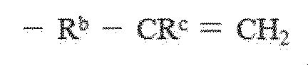
[式中、Rbは、単結合、-O-、-CO-または-OC(O)-であり、
Rcは、水素原子、炭素数1~10のアルキル基(好ましくは、炭素数1~3のアルキル基、より好ましくはメチル基)、ラクタム基(好ましくは、β-ラクタム、γ-ラクタムまたはδ-ラクタム基、より好ましくはγ-ラクタム基)またはフェニル基を表し、好ましくは、メチル基または水素原子である。]
で表される基である。
より好ましいラジカル重合性基は、下記式:

[式中、Rcは、上記と同意義である。]
で表される基である。
さらに好ましいラジカル重合性基は、アクリロイル基またはメタクリロイル基である。
本発明における当該フッ素不含有ラジカル重合性化合物の好適な例は、アクリレート単量体、およびこれに由来する構成単位を有するアクリル共重合体を包含する。
前記「フッ素不含有ラジカル重合性化合物」の例としては、
スチレン、α-メチルスチレン、
2-ブロモスチレン、酢酸ビニル、メチルビニルケトン、アクリロニトリル、N-ビニルカルバゾール、N-ビニルピロリドン、アクリレート、メチルアクリレート、n-ブチルアクリレート、ラウリルアクリレート、2-エチルヘキシルアクリレート、ジシクロペンタニルアクリレート、フェニルアクリレート、o-ビフェニルアクリレート、2-ナフチルアクリレート、エチレンオキシドフェノールアクリレート、フェノキシジエチレングリコールアクリレート、フェノキシ-ポリエチレングリコールアクリレート、ノニルフェノールエチレンオキシドアクリレート、ビスフェノールAエチレンオキシドジアクリレート、エチレンオキシドテトラブロモビスフェノールAジアクリレート、エチレンオキシドビスフェノールAジアクリレート、プロピレンオキシドビスフェノールAジアクリレート、プロポキシ化エトキシ化ビスフェノールAジアクリレート、ジメチロール-トリシクロデカンジアクリレート、プロピレンオキシドトリメチロールプロパントリアクリレート、ウレタンアクリレート、ε-カプロラクトン酸トリス-(2-アクリロキシエチル)イソシアヌレート、メトキシポリエチレングリコールアクリレート、ポリプロピレングリコール400ジアクリレート、オクトキシポリエチレングリコール-ポリプロピレングリコールモノアクリレート、トリメチロールプロパントリアクリレート、トリブロモフェニルアクリレート、エチレンオキシドトリブロモフェニルアクリレート、フェニルフェノールグリシジルエーテルアクリレート、2-メチル-2アダマンチルアクリレート、3-ヒドロキシ-1-アダマンチルアクリレート、1-アダマンチルアクリレート、フェニルエチルアクリレート、2-フェニルエチルアクリレート、2-フェノキシエチルアクリレート、2-(9-カルバゾリル)エチルアクリレート、メチルフェノキシエチルアクリレート、トリフェニルメチルチオアクリレート、2-(p-クロロフェノキシ)エチルアクリレート、ノニルフェノキシエチルアクリレート、フェノールエトキシレートモノアクリレート、p-クロロフェニルアクリレート、2-(1-ナフチルオキシ)エチルアクリレート、2,4,6-トリブロモフェニルアクリレート、イソボニルアクリレート、ヒドロキシエチルアクリレート、2-ヒドロキシ-3-フェノキシプロピルアクリレート、2,3-ジブロムプロピルアクリレート、2-(トリシクロ[5,2,102.6]ジブロモデシルチオ)エチルアクリレート、テトラメチレングリコールジアクリレート、エチレングリコールジアクリレート、ジエチレンジチオグリコールジアクリレート、トリエチレングリコールジアクリレート、テトラエチレングリコールジアクリレート、ポリエチレングリコールジアクリレート、フェノキシポリエチレングリコールアクリレート、プロピレングリコールジアクリレート、メトキシプロピレングリコールアクリレート、1,3-ブタンジオールジアクリレート、ネオペンチルグリコールジアクリレート、ヘキサンジオールジアクリレート、1,4-シクロヘキサンジオールジアクリレート、トリメチロールプロパントリアクリレート、トリメチロールエタントリアクリレート、ペンタエリスリトールジアクリレート、ペンタエリスリトールトリアクリレート、ペンタエリスリトールテトラアクリレート、ジペンタエリスリトールジアクリレート、ジペンタエリスリトールトリアクリレート、ジペンタエリスリトールテトラアクリレート、ジペンタエリスリトールヘキサアクリレート、ソルビトールトリアクリレート、ソルビトールテトラアクリレート、ソルビトールペンタアクリレート、ソルビトールヘキサアクリレート、2-エチルヘキシルカルビトールアクリレート、S-(1-ナフチルメチル)チオアクリレート、β-アクリロキシエチルハイドロゲンフタレート、エトキシ化されたビスフェノールAジアクリレート、イタコン酸、マレイン酸、N-アクリロイルモルホリン、α-シアノアクリル酸メチル、ビニル-2-クロロエチルエーテル、ビニル-n-ブチルエーテル、トリエチレングリコールジビニルエーテル、トリメチロールエタントリビニルエーテル、1,4-シクロヘキサンジメタノールジビニルエーテル、トリメチロールプロパントリ(アクリロイルオキシプロピル)エーテル、ビスフェノールAの(2-アクリルオキシエチル)エーテル、ビス(4-アクリロキシジエトキシフェニル)メタン、ビス(4-アクリロキシエトキシ-3,5-ジブロモフェニル)メタン、2,2-ビス(4-アクリロキシエトキシフェニル)プロパン、2,2-ビス(4-アクリロキシジエトキシフェニル)プロパン、2,2-ビス(4-アクリロキシエトキシ-3,5-ジブロモフェニル)プロパン、2,3-ナフタレンジカルボン酸(アクリロキシエチル)モノエステル、2,3-ナフタリンジカルボン酸(2-アクリロキシエチル)(3-アクリロキシプロピル-2-ヒドロキシ)ジエステル、4,5-フェナントレンジカルボン酸(2-アクリロキシエチル)(3-アクリロキシプロピル-2-ヒドロキシ)ジエステル、ジフェン酸(2-メタクリロキシエチル)モノエステル、ジフェン酸(2-アクリロキシエチル)(3-アクリロキシプロピル-2-ヒドロキシ)ジエステル、1,3-ビス[2-アクリロキシ-3-(2,4,6-トリブロモフェノキシ)プロポキシ]ベンゼン、ビス(4-アクリロキシエトキシフェニル)スルホン、ビス(4-アクリロキシジエトキシフェニル)スルホン、ビス(4-アクリロキシプロポキシフェニル)スルホン、ビス(4-アクリロキシエトキシ-3,5-ジブロモフェニル)スルホン、および4,4’-ビス(β-アクリロイルオキシエチルチオ)ジフェニルスルホン
ならびに前記化合物におけるアクリレートをメタクリレートに変えた化合物などが挙げられる。(メタ)アクリル酸とジオールとのエステル基を有する化合物としては、具体的には、下記化学式:

(化学式中、q及びpは同一又は異なり0~6であってq+p=2~6となる数、R3及びR4は同一又は異なり水素原子又はメチル基)が挙げられる。
q+pが5であると、より好ましい。具体的には、
9,9-ビス(4-アクリロキシジプロポキシフェニル)フルオレン、
9,9-ビス(4-アクリロキシエトキシ-3,5-ジメチル)フルオレン、
9,9-ビス(4-アクリロキシトリエトキシフェニル)フルオレン、
9,9-ビス(4-アクリロキシエトキシ-3-メチルフェニル)フルオレン、
9,9-ビス(4-アクリロキシエトキシ-3-エチルフェニル)フルオレン、および
9,9-ビス(4-アクリロキシジエトキシフェニル)フルオレン
などが挙げられる。
フッ素不含有ラジカル重合性化合物は、ラジカル重合性基を有する化合物である。
好ましいラジカル重合性基は、下記式:
Rcは、水素原子、炭素数1~10のアルキル基(好ましくは、炭素数1~3のアルキル基、より好ましくはメチル基)、ラクタム基(好ましくは、β-ラクタム、γ-ラクタムまたはδ-ラクタム基、より好ましくはγ-ラクタム基)またはフェニル基を表し、好ましくは、メチル基または水素原子である。]
で表される基である。
より好ましいラジカル重合性基は、下記式:
で表される基である。
さらに好ましいラジカル重合性基は、アクリロイル基またはメタクリロイル基である。
本発明における当該フッ素不含有ラジカル重合性化合物の好適な例は、アクリレート単量体、およびこれに由来する構成単位を有するアクリル共重合体を包含する。
前記「フッ素不含有ラジカル重合性化合物」の例としては、
スチレン、α-メチルスチレン、
2-ブロモスチレン、酢酸ビニル、メチルビニルケトン、アクリロニトリル、N-ビニルカルバゾール、N-ビニルピロリドン、アクリレート、メチルアクリレート、n-ブチルアクリレート、ラウリルアクリレート、2-エチルヘキシルアクリレート、ジシクロペンタニルアクリレート、フェニルアクリレート、o-ビフェニルアクリレート、2-ナフチルアクリレート、エチレンオキシドフェノールアクリレート、フェノキシジエチレングリコールアクリレート、フェノキシ-ポリエチレングリコールアクリレート、ノニルフェノールエチレンオキシドアクリレート、ビスフェノールAエチレンオキシドジアクリレート、エチレンオキシドテトラブロモビスフェノールAジアクリレート、エチレンオキシドビスフェノールAジアクリレート、プロピレンオキシドビスフェノールAジアクリレート、プロポキシ化エトキシ化ビスフェノールAジアクリレート、ジメチロール-トリシクロデカンジアクリレート、プロピレンオキシドトリメチロールプロパントリアクリレート、ウレタンアクリレート、ε-カプロラクトン酸トリス-(2-アクリロキシエチル)イソシアヌレート、メトキシポリエチレングリコールアクリレート、ポリプロピレングリコール400ジアクリレート、オクトキシポリエチレングリコール-ポリプロピレングリコールモノアクリレート、トリメチロールプロパントリアクリレート、トリブロモフェニルアクリレート、エチレンオキシドトリブロモフェニルアクリレート、フェニルフェノールグリシジルエーテルアクリレート、2-メチル-2アダマンチルアクリレート、3-ヒドロキシ-1-アダマンチルアクリレート、1-アダマンチルアクリレート、フェニルエチルアクリレート、2-フェニルエチルアクリレート、2-フェノキシエチルアクリレート、2-(9-カルバゾリル)エチルアクリレート、メチルフェノキシエチルアクリレート、トリフェニルメチルチオアクリレート、2-(p-クロロフェノキシ)エチルアクリレート、ノニルフェノキシエチルアクリレート、フェノールエトキシレートモノアクリレート、p-クロロフェニルアクリレート、2-(1-ナフチルオキシ)エチルアクリレート、2,4,6-トリブロモフェニルアクリレート、イソボニルアクリレート、ヒドロキシエチルアクリレート、2-ヒドロキシ-3-フェノキシプロピルアクリレート、2,3-ジブロムプロピルアクリレート、2-(トリシクロ[5,2,102.6]ジブロモデシルチオ)エチルアクリレート、テトラメチレングリコールジアクリレート、エチレングリコールジアクリレート、ジエチレンジチオグリコールジアクリレート、トリエチレングリコールジアクリレート、テトラエチレングリコールジアクリレート、ポリエチレングリコールジアクリレート、フェノキシポリエチレングリコールアクリレート、プロピレングリコールジアクリレート、メトキシプロピレングリコールアクリレート、1,3-ブタンジオールジアクリレート、ネオペンチルグリコールジアクリレート、ヘキサンジオールジアクリレート、1,4-シクロヘキサンジオールジアクリレート、トリメチロールプロパントリアクリレート、トリメチロールエタントリアクリレート、ペンタエリスリトールジアクリレート、ペンタエリスリトールトリアクリレート、ペンタエリスリトールテトラアクリレート、ジペンタエリスリトールジアクリレート、ジペンタエリスリトールトリアクリレート、ジペンタエリスリトールテトラアクリレート、ジペンタエリスリトールヘキサアクリレート、ソルビトールトリアクリレート、ソルビトールテトラアクリレート、ソルビトールペンタアクリレート、ソルビトールヘキサアクリレート、2-エチルヘキシルカルビトールアクリレート、S-(1-ナフチルメチル)チオアクリレート、β-アクリロキシエチルハイドロゲンフタレート、エトキシ化されたビスフェノールAジアクリレート、イタコン酸、マレイン酸、N-アクリロイルモルホリン、α-シアノアクリル酸メチル、ビニル-2-クロロエチルエーテル、ビニル-n-ブチルエーテル、トリエチレングリコールジビニルエーテル、トリメチロールエタントリビニルエーテル、1,4-シクロヘキサンジメタノールジビニルエーテル、トリメチロールプロパントリ(アクリロイルオキシプロピル)エーテル、ビスフェノールAの(2-アクリルオキシエチル)エーテル、ビス(4-アクリロキシジエトキシフェニル)メタン、ビス(4-アクリロキシエトキシ-3,5-ジブロモフェニル)メタン、2,2-ビス(4-アクリロキシエトキシフェニル)プロパン、2,2-ビス(4-アクリロキシジエトキシフェニル)プロパン、2,2-ビス(4-アクリロキシエトキシ-3,5-ジブロモフェニル)プロパン、2,3-ナフタレンジカルボン酸(アクリロキシエチル)モノエステル、2,3-ナフタリンジカルボン酸(2-アクリロキシエチル)(3-アクリロキシプロピル-2-ヒドロキシ)ジエステル、4,5-フェナントレンジカルボン酸(2-アクリロキシエチル)(3-アクリロキシプロピル-2-ヒドロキシ)ジエステル、ジフェン酸(2-メタクリロキシエチル)モノエステル、ジフェン酸(2-アクリロキシエチル)(3-アクリロキシプロピル-2-ヒドロキシ)ジエステル、1,3-ビス[2-アクリロキシ-3-(2,4,6-トリブロモフェノキシ)プロポキシ]ベンゼン、ビス(4-アクリロキシエトキシフェニル)スルホン、ビス(4-アクリロキシジエトキシフェニル)スルホン、ビス(4-アクリロキシプロポキシフェニル)スルホン、ビス(4-アクリロキシエトキシ-3,5-ジブロモフェニル)スルホン、および4,4’-ビス(β-アクリロイルオキシエチルチオ)ジフェニルスルホン
ならびに前記化合物におけるアクリレートをメタクリレートに変えた化合物などが挙げられる。(メタ)アクリル酸とジオールとのエステル基を有する化合物としては、具体的には、下記化学式:
q+pが5であると、より好ましい。具体的には、
9,9-ビス(4-アクリロキシジプロポキシフェニル)フルオレン、
9,9-ビス(4-アクリロキシエトキシ-3,5-ジメチル)フルオレン、
9,9-ビス(4-アクリロキシトリエトキシフェニル)フルオレン、
9,9-ビス(4-アクリロキシエトキシ-3-メチルフェニル)フルオレン、
9,9-ビス(4-アクリロキシエトキシ-3-エチルフェニル)フルオレン、および
9,9-ビス(4-アクリロキシジエトキシフェニル)フルオレン
などが挙げられる。
[規則26に基づく補充 28.09.2016]
前記「フッ素不含有ラジカル重合性化合物」の例としては、さらに、ジアリルフタレートモノマーである、
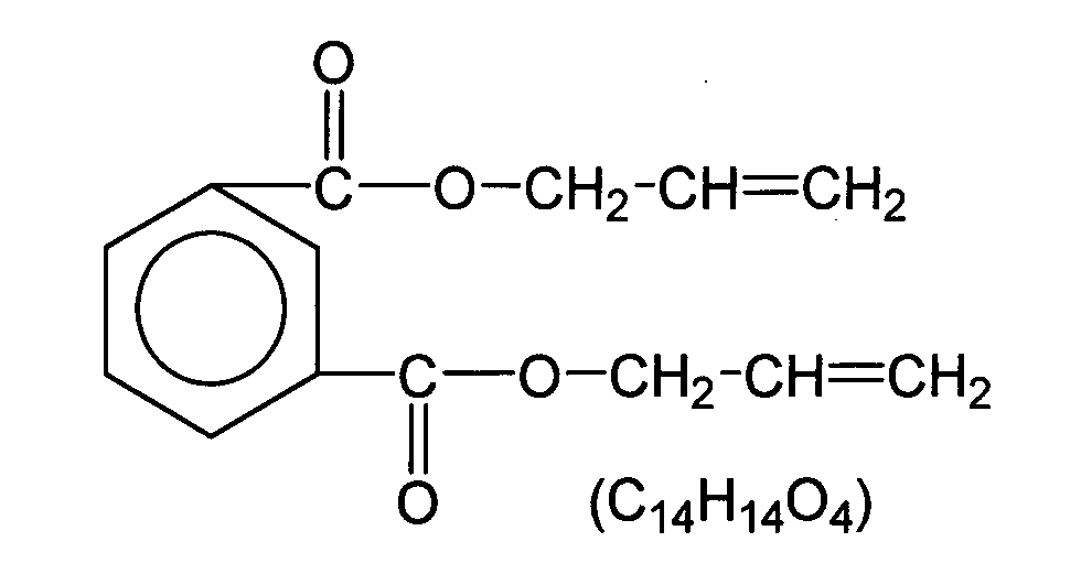
および
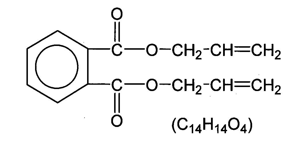
が挙げられる。
前記「フッ素不含有ラジカル重合性化合物」の例としては、さらに、2,4-ビス(β-アクリロイルオキシエチルチオ)ジフェニルケトン、4,4’-ビス(β-アクリロイルオキシエチルチオ)ジフェニルケトン、4,4’-ビス(β-アクリロイルオキシエチルチオ)ジフェニルケトン、トリ(アクリロイルオキシエチル)イソシアヌレート、アクリルアミド、メチレンビスアクリルアミド、ジアセトンアクリルアミド、シクロヘキセンオキシド、エトキシ化プロピレングリコール700ジアクリレート、プロポキシ化エトキシ化ジアクリレート、デンドリマー(2世代)アクリレート、および前記におけるアクリレートをメタクリレートに変えた化合物などが挙げられる。
前記「フッ素不含有ラジカル重合性化合物」の例は、前記で例示したこれらに限定されるものではなく、記録感度や多重記録性の点から、9,9-ビス(4-アクリロキシジプロポキシフェニル)フルオレン、ジアリルフタレートモノマー、プロポキシ化エトキシ化ビスフェノールAジアクリレート、ポリプロピレングリコール700ジアクリレート、α-フルオロアクリロイル基またはアクリロイル基を有するものおよび前記におけるアクリレートをメタクリレートに変えた化合物などが好ましい。
前記「フッ素不含有ラジカル重合性化合物」の例としては、さらに、ジアリルフタレートモノマーである、
前記「フッ素不含有ラジカル重合性化合物」の例としては、さらに、2,4-ビス(β-アクリロイルオキシエチルチオ)ジフェニルケトン、4,4’-ビス(β-アクリロイルオキシエチルチオ)ジフェニルケトン、4,4’-ビス(β-アクリロイルオキシエチルチオ)ジフェニルケトン、トリ(アクリロイルオキシエチル)イソシアヌレート、アクリルアミド、メチレンビスアクリルアミド、ジアセトンアクリルアミド、シクロヘキセンオキシド、エトキシ化プロピレングリコール700ジアクリレート、プロポキシ化エトキシ化ジアクリレート、デンドリマー(2世代)アクリレート、および前記におけるアクリレートをメタクリレートに変えた化合物などが挙げられる。
前記「フッ素不含有ラジカル重合性化合物」の例は、前記で例示したこれらに限定されるものではなく、記録感度や多重記録性の点から、9,9-ビス(4-アクリロキシジプロポキシフェニル)フルオレン、ジアリルフタレートモノマー、プロポキシ化エトキシ化ビスフェノールAジアクリレート、ポリプロピレングリコール700ジアクリレート、α-フルオロアクリロイル基またはアクリロイル基を有するものおよび前記におけるアクリレートをメタクリレートに変えた化合物などが好ましい。
当該フッ素含有ラジカル重合性化合物は、ラジカル重合性基を有する化合物である。
好ましいラジカル重合性基は、下記式:
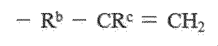
[式中、Rbは、単結合、-O-、-CO-または-OC(O)-であり、
Rcは、水素原子、フッ素原子、あるいはフッ素原子により置換されていてもよい炭素数1~10のアルキル基(好ましくは、炭素数1~3のアルキル基、より好ましくはメチル基)、ラクタム基(好ましくは、β-ラクタム、γ-ラクタムまたはδ-ラクタム基、より好ましくはγ-ラクタム基)またはフェニル基を表し、好ましくは、メチル基または水素原子である。]
で表される基である。
より好ましいラジカル重合性基は、下記式:

[式中、Rcは、上記と同意義である。]
で表される基である。
さらに好ましいラジカル重合性基は、アクリロイル基またはメタクリロイル基である。
本発明における当該フッ素含有ラジカル重合性化合物の好適な例は、フッ素含有基を有するアクリレート単量体、およびこれに由来する構成単位を有するアクリル共重合体を包含する。
好ましいラジカル重合性基は、下記式:
Rcは、水素原子、フッ素原子、あるいはフッ素原子により置換されていてもよい炭素数1~10のアルキル基(好ましくは、炭素数1~3のアルキル基、より好ましくはメチル基)、ラクタム基(好ましくは、β-ラクタム、γ-ラクタムまたはδ-ラクタム基、より好ましくはγ-ラクタム基)またはフェニル基を表し、好ましくは、メチル基または水素原子である。]
で表される基である。
より好ましいラジカル重合性基は、下記式:
で表される基である。
さらに好ましいラジカル重合性基は、アクリロイル基またはメタクリロイル基である。
本発明における当該フッ素含有ラジカル重合性化合物の好適な例は、フッ素含有基を有するアクリレート単量体、およびこれに由来する構成単位を有するアクリル共重合体を包含する。
フッ素含有基を有するアクリレート単量体は、例えば、式(4):

[式中、Xは、水素原子、メチル基、フッ素原子、塩素原子、臭素原子、ヨウ素原子、CFX1X2基(但し、X1およびX2は、水素原子、フッ素原子、塩素原子、臭素原子またはヨウ素原子である。)、シアノ基、炭素数1~21の直鎖状または分岐状のフルオロアルキル基、置換または非置換のベンジル基、置換または非置換のフェニル基、
Yは、直接結合、酸素原子を有していてもよい炭素数1~10の脂肪族基、酸素原子を有していてもよい炭素数6~10の芳香族基、環状脂肪族基または芳香脂肪族基、-CH2CH2N(R1)SO2-基(但し、R1は炭素数1~4のアルキル基である。)または-CH2CH(OY1)CH2-基(但し、Y1は水素原子またはアセチル基である。)、
Rfは炭素数1~7の直鎖状または分岐状のフルオロアルキル基、炭素数2~7のフルオロアルケニル基または、繰り返し単位:-C3F6O-、-C2F4O-および-CF2O-からなる群から選択された少なくとも一種の繰り返し単位の合計数が1~200のフルオロエーテル基である。]
で示される。
好ましくは、Xは水素原子またはメチル基である。
Yは、直接結合、酸素原子を有していてもよい炭素数1~10の脂肪族基、酸素原子を有していてもよい炭素数6~10の芳香族基、環状脂肪族基または芳香脂肪族基、-CH2CH2N(R1)SO2-基(但し、R1は炭素数1~4のアルキル基である。)または-CH2CH(OY1)CH2-基(但し、Y1は水素原子またはアセチル基である。)、
Rfは炭素数1~7の直鎖状または分岐状のフルオロアルキル基、炭素数2~7のフルオロアルケニル基または、繰り返し単位:-C3F6O-、-C2F4O-および-CF2O-からなる群から選択された少なくとも一種の繰り返し単位の合計数が1~200のフルオロエーテル基である。]
で示される。
好ましくは、Xは水素原子またはメチル基である。
式(I)において、Rf基がフルオロアルキル基の場合、パーフルオロアルキル基であることが好ましい。Rf基の例としては、-CF3、-CF2CF3、-CF2CF2CF3、-CF(CF3)2、-CF2CF2CF2CF3、-CF2CF(CF3)2、-C(CF3)3、-(CF2)4CF3、-(CF2)2CF(CF3)2、-CF2C(CF3)3、-CF(CF3)CF2CF2CF3、-(CF2)5CF3、-(CF2)3CF(CF3)2、-(CF2)4CF(CF3)2、-(CF2)2H、-CF2CFHCF3、-(CF2)4H、及び-(CF2)6H等が挙げられる。Rf基がフルオロアルキル基である場合に、先述したPFOAの観点および機能の観点から、Rf基の炭素数は、1~7、例えば2~6、特に4~6、特別には6であることが好ましい。
Rf基がフルオロアルケニル基の場合、パーフルオロアルケニル基であることが好ましい。Rf基の例は、-CF=CF(CF3)、-CF=C(CF3)2、-CF=C(CF3)(CF2CF2CF3)、-CF=C(CF3)(CF(CF3)2)、-C(CF3)=CF(CF(CF3)2)、-C(CF2CF3)=C(CF3)2等である。Rf基がフルオロアルケニル基である場合に、Rf基の炭素数は、2~7、特に3~6、特別には6であることが好ましい。
Rf基がフルオロアルケニル基の場合、パーフルオロアルケニル基であることが好ましい。Rf基の例は、-CF=CF(CF3)、-CF=C(CF3)2、-CF=C(CF3)(CF2CF2CF3)、-CF=C(CF3)(CF(CF3)2)、-C(CF3)=CF(CF(CF3)2)、-C(CF2CF3)=C(CF3)2等である。Rf基がフルオロアルケニル基である場合に、Rf基の炭素数は、2~7、特に3~6、特別には6であることが好ましい。
Rf基がフルオロエーテル基の場合、フルオロエーテル基は、-C3F6O-、-C2F4O-および-CF2O-からなる群から選択された少なくとも一種の繰り返し単位(オキシパーフルオロアルキレン基)を有する。-C3F6O-は-CF2CF2CF2O-または-CF2C(CF3)FO-である。-C2F4O-は一般に-CF2CF2O-である。オキシパーフルオロアルキレン繰り返し単位の合計数は、1~200、例えば1~100、特に5~50である。フルオロエーテル基は、オキシパーフルオロアルキレン繰り返し単位に直接に結合する末端基を有する。末端基の例は、水素原子、ハロゲン原子(例えば、フッ素原子)、アルコール基(例えば、HOCH2-)、アミン基(例えば、H2N-)、クロロメチル基(ClH2C-)である。フルオロエーテル基は、オキシパーフルオロアルキレン繰り返し単位および末端基に加えて、炭素数1~10のフルオロアルキレン基、特にパーフルオロアルキレン基を有していてもよい。炭素数1~10のフルオロアルキレン基の例は、-CF2-および-CF2CF2-である。
Rf基の例であるフルオロエーテル基(特に、パーフルオロエーテル基)の例は、次のとおりである。
F-(CF2CF2CF2O)n-CF2CF2- (nは1~200)
F-(CF2C(CF3)FO)n-CF2CF2- (nは1~200)
F-(CF2C(CF3)FO)n-(CF2O)m-CF2CF2- (nとmの合計は1~200)
F-(CF2CF2O)n-(CF2O)m-CF2CF2- (nとmの合計は1~200)
F-(CF2CF2CF2O)n-CF2CF2- (nは1~200)
F-(CF2C(CF3)FO)n-CF2CF2- (nは1~200)
F-(CF2C(CF3)FO)n-(CF2O)m-CF2CF2- (nとmの合計は1~200)
F-(CF2CF2O)n-(CF2O)m-CF2CF2- (nとmの合計は1~200)
Yは、直接結合、酸素原子を有していてもよい炭素数1~10の脂肪族基、酸素原子を有していてもよい炭素数6~10の芳香族基、環状脂肪族基または芳香脂肪族基、-CH2CH2N(R1)SO2-基(但し、R1は炭素数1~4のアルキル基である。)または-CH2CH(OY1)CH2-基(但し、Y1は水素原子またはアセチル基である。)である。脂肪族基はアルキレン基(特に炭素数1~4、例えば、1または2)であることが好ましい。芳香族基、環状脂肪族基および芳香脂肪族基は、置換されていてもあるいは置換されていなくてもどちらでもよい。
前記フッ素含有基を有するアクリレート単量体の例は、次のとおりである。
Rf-(CH2)10OCOCH=CH2
Rf-(CH2)10OCOC(CH3)=CH2
Rf-CH2OCOCH=CH2
Rf-CH2OCOC(CH3)=CH2
Rf-(CH2)2OCOCH=CH2
Rf-(CH2)2OCOC(CH3)=CH2
Rf-SO2N(CH3)(CH2)2OCOCH=CH2
Rf-SO2N(C2H5)(CH2)2OCOCH=CH2
Rf-CH2CH(OCOCH3)CH2OCOC(CH3)=CH2
Rf-CH2CH(OH)CH2OCOCH=CH2

Rf-(CH2)10OCOCH=CH2
Rf-(CH2)10OCOC(CH3)=CH2
Rf-CH2OCOCH=CH2
Rf-CH2OCOC(CH3)=CH2
Rf-(CH2)2OCOCH=CH2
Rf-(CH2)2OCOC(CH3)=CH2
Rf-SO2N(CH3)(CH2)2OCOCH=CH2
Rf-SO2N(C2H5)(CH2)2OCOCH=CH2
Rf-CH2CH(OCOCH3)CH2OCOC(CH3)=CH2
Rf-CH2CH(OH)CH2OCOCH=CH2
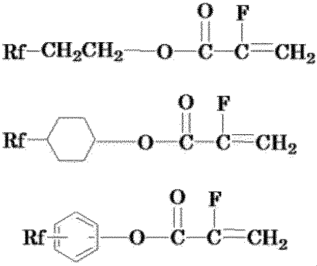
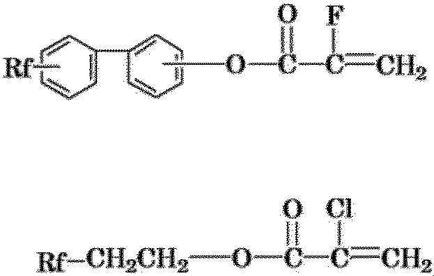

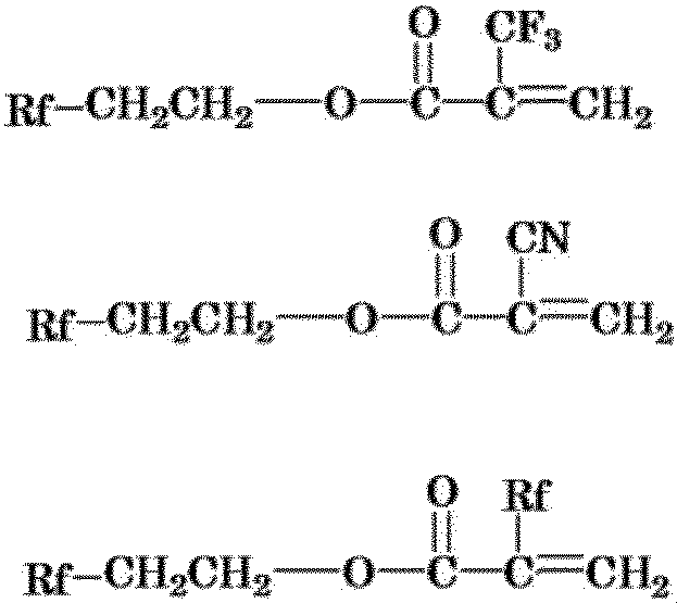

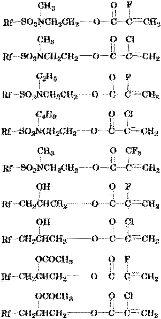
[式中、Rfは炭素数1~7の直鎖状または分岐状のフルオロアルキル基、炭素数2~7のフルオロアルケニル基または、繰り返し単位:-C3F6O-、-C2F4O-および-CF2O-からなる群から選択された少なくとも一種の繰り返し単位の合計数が1~200のフルオロエーテル基である。]
カチオン重合触媒としては、例えば、芳香族ジアゾニウム塩、芳香族ヨードニウム塩、芳香族スルホニウム塩、芳香族ホスホニウム塩、混合配位子金属塩、芳香族オニウム塩、が例示される。例えばサンエイドSI-60L、同80L、同110L(何れも三新化学工業社製:商品名)などが挙げられる。
本発明で用いられる「非線形吸収色素」の二光子吸収断面積は、波長が365nm~650nmの範囲にある特定の波長において、
50~100000×10-50cm4・s・molecule-1・photon-1の範囲内である必要があり、好ましくは100~90000×10-50cm4・s・molecule-1・photon-1の範囲内、より好ましくは150~70000×10-50cm4・s・molecule-1・photon-1の範囲内、およびより更に好ましくは200~60000×10-50cm4・s・molecule-1・photon-1の範囲内である。
本発明の光情報記録媒体は、当該非線形吸収色素を含有することに基づき、前記パルス光レーザーの照射により、高速(短時間)で、当該干渉縞を局所的に破壊することにより、記録マークを形成できる。
本発明で用いられる「非線形吸収色素」の二光子吸収断面積は、波長が365nm~650nmの範囲にある特定の波長において、
50~100000×10-50cm4・s・molecule-1・photon-1の範囲内である必要があり、好ましくは100~90000×10-50cm4・s・molecule-1・photon-1の範囲内、より好ましくは150~70000×10-50cm4・s・molecule-1・photon-1の範囲内、およびより更に好ましくは200~60000×10-50cm4・s・molecule-1・photon-1の範囲内である。
本発明の光情報記録媒体は、当該非線形吸収色素を含有することに基づき、前記パルス光レーザーの照射により、高速(短時間)で、当該干渉縞を局所的に破壊することにより、記録マークを形成できる。
本発明で用いられる「非線形吸収色素」は、非線形吸収に基づくものとして、好ましくは、1個以上の置換基を有していてもよい、2個以上のベンゼン環を有する炭化水素であり、1個以上の置換基を有していてもよい、縮環系芳香族炭化水素である。
当該「炭化水素」の好ましい具体例は、ナフタレン、アントラセン、フェナントレン、1,4-ビス(フェニルエチニル)ベンゼン、およびピレンを包含する。
当該「置換基」の例は、ハロゲン原子、ヒドロキシ基、および有機基を包含する。
本発明で用いられる「非線形吸収色素」の具体例は、1,1,4,4-テトラフェニル-1,3-ブタジエン、1,3,6,8-テトラフェニルピレン、ピレン-エチレングリコール-ピレン、1,4-ビス(フェニルエチニル)ベンゼン、1,2,4,5-テトラキス(フェニルエチニル)ベンゼン、9,10-ジフェニルアントラセン、5,6,11,12-テトラフェニルナフタセン、フルオレン、2,7-ジブロモフルオレン、1-ブロモピレン、4-ブロモピレンを包含し、その好ましい具体例は、1,4-ビス(フェニルエチニル)ベンゼン、およびピレンを包含する。
当該「炭化水素」の好ましい具体例は、ナフタレン、アントラセン、フェナントレン、1,4-ビス(フェニルエチニル)ベンゼン、およびピレンを包含する。
当該「置換基」の例は、ハロゲン原子、ヒドロキシ基、および有機基を包含する。
本発明で用いられる「非線形吸収色素」の具体例は、1,1,4,4-テトラフェニル-1,3-ブタジエン、1,3,6,8-テトラフェニルピレン、ピレン-エチレングリコール-ピレン、1,4-ビス(フェニルエチニル)ベンゼン、1,2,4,5-テトラキス(フェニルエチニル)ベンゼン、9,10-ジフェニルアントラセン、5,6,11,12-テトラフェニルナフタセン、フルオレン、2,7-ジブロモフルオレン、1-ブロモピレン、4-ブロモピレンを包含し、その好ましい具体例は、1,4-ビス(フェニルエチニル)ベンゼン、およびピレンを包含する。
一方、本発明で用いられる「光増感剤」は、光干渉縞に基づくものとして、光重合開始剤を増感するものであれば特に限定されず、公知のものを使用できる。例えば、チオピリリウム塩系化合物、メロシアニン系化合物、キノリン系化合物、スチリルキノリン系化合物、クマリン系化合物、ケトクマリン系化合物、チオキサンテン系化合物、キサンテン系化合物、オキソノール系化合物、シアニン系化合物、ローダミン系化合物、ピリリウム塩系化合物等が例示される。光増感剤は、光学素子のような高透明性が要求される場合には、ホログラム記録後の後工程、加熱や紫外線照射により分解し無色透明になるものが好ましい。光増感剤は単独で又は2種以上組み合わせて使用できる。
代表的に、スチリル系化合物あるいはクマリン系化合物が好ましく、具体的には、2-(p-ジメチルアミノスチリル)キノリン、2-(p-ジエチルアミノスチリル)キノリン、4-(p-ジメチルアミノスチリル)キノリン、4-(p-ジエチルアミノスチリル)キノリン、2-(p-ジメチルアミノスチリル)-3,3-3H-インドール、2-(p-ジエチルアミノスチリル)-3,3-3H-インドール、2-(p-ジメチルアミノスチリル)ベンズオキサゾール、2-(p-ジエチルアミノスチリル)ベンズオキサゾール、2-(p-ジメチルアミノスチリル)べンズイミダゾール、2-(p-ジエチルアミノスチリル)ベンズイミダゾールなどが挙げられる。
また、クマリン系化合物としては、7-ジエチルアミノ-4-メチルクマリン、7-エチルアミノ-4-トリフルオロメチルクマリン、4,6-ジエチルアミノ-7-エチルアミノクマリン、3-(2-ベンズイミダゾリル)-7-N,N-ジエチルアミノクマリン、7-ジエチルアミノシクロペンタ(c)クマリン、7-アミノ-4-トリフルオロメチルクマリン、1,2,3,4,5,3H,6H,10H-テトラヒドロ-8-トリフルオロメチル(1)ベンゾピラノ-(9,9A,1-gh)-キノリジン-10-オン、7-エチルアミノ-6-メチル-4-トリフルオロメチルクマリン、1,2,3,4,5,3H,6H,10H-テトラヒドロ-9-カルベトキシ(1)ベンゾピラノ(9,9a,1-gh)-キノリジン-10-オンなどが挙げられる。
また、前記光重合開始剤としては、光ラジカル重合を活性化する化合物であれば特に限定されず、例えば、t-ブチルペルオキシベンゾエートなどの過酸化エステル類;t-ブチルヒドロペルオキシド、ジ-t-ブチルペルオキシドなどの過酸化物類;ベンゾイン、ベンゾインメチルエーテル、ベンゾインエチルエーテル、ベンゾインイソプロピルエーテルなどのベンゾイン・ベンゾインアルキルエーテル類;アセトフェノン、2,2-ジメトキシ-2-フェニルアセトフェノン、2,2-ジエトキシ-2-フェニルアセトフェノン、1,1-ジクロロアセトフェノン、2-メチル-1-[4-(メチルチオ)フェニル]-2-モルフォリノ-プロパン-1-オン、2-ベンジル-2-ジメチルアミノ-1-(4-モルフォリノフェニル)-ブタン-1-オンなどのアセトフェノン類;2-メチルアントラキノン、2-エチルアントラキノン、2-ターシャリーブチルアントラキノン、1-クロロアントラキノン、2-アミルアントラキノンなどのアントラキノン類;2,4-ジメチルチオキサントン、2,4-ジエチルチオキサントン、2-クロロチオキサントン、2,4-イソプロピルチオキサントンなどのチオキサントン類;アセトフェノンジメチルケタール、ベンジルジメチルケタールなどのケタール類;ベンゾフェノンなどのベンゾフェノン類;キサントン類;ベンゾフェノン類、ベンゾインアルキルケタール類や一般名チタノセンとして知られるCGI-784(チバガイギー社製:商品名)などが挙げられ、これらを単独、もしくは光増感剤と併用して用いることができる。
これらの調製方法から理解される本発明の光情報記録材料用組成物の例を包含する、本発明の光情報記録材料用組成物、他の成分を含有してもよい。
他の成分の一例としては、可塑剤が挙げられる。
このような可塑剤としては、例えば、ジメチルテレフタレート、ジエチルテレフタレート、ジメチルフタレ一ト、ジオクチルフタレートに代表されるフタル酸エステル類;ジメチルアジペート、ジエチルアジペート、ジブチルアジペート、ジメチルセバケート、ジエチルセバケート、ジブチルセバケート、ジエチルサクシネートに代表される脂肪族二塩基酸エステル類;トリメチルホスフェート、トリエチルホスフェート、トリフェニルホスフェート、トリクレジルホスフェートに代表される正リン酸エステル類;グリセリルトリアセテート、2-エチルヘキシルアセテートに代表される酢酸エステル類;トリフェニルホスファイト、ジブチルハイドロジエンホスファイトに代表される亜リン酸エステル類等の不活性化合物、および酢酸-2-エトキシエチル、ならびにこれらの2種以上の組み合わせが例示される。
これらの調製方法から理解される本発明の光情報記録材料用組成物の例を包含する、本発明の光情報記録材料用組成物、他の成分を含有してもよい。
他の成分の一例としては、可塑剤が挙げられる。
このような可塑剤としては、例えば、ジメチルテレフタレート、ジエチルテレフタレート、ジメチルフタレ一ト、ジオクチルフタレートに代表されるフタル酸エステル類;ジメチルアジペート、ジエチルアジペート、ジブチルアジペート、ジメチルセバケート、ジエチルセバケート、ジブチルセバケート、ジエチルサクシネートに代表される脂肪族二塩基酸エステル類;トリメチルホスフェート、トリエチルホスフェート、トリフェニルホスフェート、トリクレジルホスフェートに代表される正リン酸エステル類;グリセリルトリアセテート、2-エチルヘキシルアセテートに代表される酢酸エステル類;トリフェニルホスファイト、ジブチルハイドロジエンホスファイトに代表される亜リン酸エステル類等の不活性化合物、および酢酸-2-エトキシエチル、ならびにこれらの2種以上の組み合わせが例示される。
段階(2)当該組成物のエポキシ基含有カチオン重合性物質の硬化
硬化は、エポキシ基含有カチオン重合性物質の種類に応じた方法を採用しておこなえばよい。
例えば、エポキシ基含有カチオン重合性物質は、カチオン重合触媒によって硬化される。熱カチオン重合触媒の場合の硬化は、適当な時間、および温度条件での加熱によって行うことができる。
硬化は、エポキシ基含有カチオン重合性物質の種類に応じた方法を採用しておこなえばよい。
例えば、エポキシ基含有カチオン重合性物質は、カチオン重合触媒によって硬化される。熱カチオン重合触媒の場合の硬化は、適当な時間、および温度条件での加熱によって行うことができる。
段階(2)は、例えば、前記組成物を基材上に塗工して付し、加熱によって脂環式エポキシ基含有カチオン重合性物質をカチオン重合させて硬化させる工程である。
段階(3)回折格子の形成
当該段階では、好ましくは光情報記録領域となる当該硬化物の全体に渡って回折格子を形成させる。本明細書中、これを初期化とも呼ぶ。
段階(3)回折格子の形成
当該段階では、好ましくは光情報記録領域となる当該硬化物の全体に渡って回折格子を形成させる。本明細書中、これを初期化とも呼ぶ。
本発明の光情報記録媒体が有する回折格子の層は、互いにコヒーレンスを有する2本の光を用いた光干渉露光によって、形成される。
回折格子を形成する2本の光が成す角、即ち交差角は、共に平行でかつ波面の進行方向が同じ方向である場合に成す角を0°とする定義において、互いに90°~270°の範囲内にあり、望ましくは135°~225°の範囲内にあり、更に望ましくは170°~190°の範囲にある。
光照射の条件は、光情報記録材料が含有する物質に応じて、適宜、適当な条件を採用できるが、例えば、400~650nmの範囲内の波長、および1~1000mW/cm2の範囲内の強度の光を、および0.1~2000秒の範囲内の時間照射することによって、干渉縞の層を形成できる。
回折格子の層の数は、光情報記録材料の膜厚および交差角により調整できる。
回折格子を形成する2本の光が成す角、即ち交差角は、共に平行でかつ波面の進行方向が同じ方向である場合に成す角を0°とする定義において、互いに90°~270°の範囲内にあり、望ましくは135°~225°の範囲内にあり、更に望ましくは170°~190°の範囲にある。
光照射の条件は、光情報記録材料が含有する物質に応じて、適宜、適当な条件を採用できるが、例えば、400~650nmの範囲内の波長、および1~1000mW/cm2の範囲内の強度の光を、および0.1~2000秒の範囲内の時間照射することによって、干渉縞の層を形成できる。
回折格子の層の数は、光情報記録材料の膜厚および交差角により調整できる。
本発明の光情報記録材料の、405nmでの吸収係数は、以下の方法で測定した場合、好ましくは150cm-1以下、より好ましくは100cm-1以下、更に好ましくは50cm-1以下である。
(吸収係数の測定方法)
吸収係数は前記数式1に規定される方法で、試料の透過率Tおよび試料の厚さLより求められる。
(吸収係数の測定方法)
吸収係数は前記数式1に規定される方法で、試料の透過率Tおよび試料の厚さLより求められる。
本発明の光情報記録材料は、光情報記録材料が、後述する段階(4)の操作により、光情報記録材料全体にわたって記録マークを形成しやすい観点から、波長が365nm~650nmの範囲にある特定の波長において、好ましくは50%以上、より好ましくは60%、および更に好ましくは70%の可視光線透過率を有する。
本明細書中、可視光線透過率の値は、JIS K 7375:2008に記載の測定方法によって決定される。
本明細書中、可視光線透過率の値は、JIS K 7375:2008に記載の測定方法によって決定される。
光情報記録材料の形状は、特に限定されないが、例えば、平板状であることができる。
当該平板状の光情報記録材料において、好適には、前記「多層の回折格子」または「多層の干渉縞」は、当該平板の平面方向に平行に配置されていることができる。
当該平板状の光情報記録材料において、その厚さは、通常、50~600μmの範囲内である。
段階(4)記録マークの形成
記録マークの形成は、段階(3)で初期化した光情報記録材料に、
0.1~30ナノ秒の範囲内のパルス幅、365~650nmの範囲内の波長、および1000W以下のピーク出力を有するパルスレーザー光を照射することにより形成される。
具体的には、段階(3)で形成された多層の干渉縞を、局所的に破壊することにより、記録マークを形成できる。
この光情報記録材料は、段階(3)の操作により初期化されることで、情報を再生する際に読出光を照射すると、媒体から再生光が戻るが、段階(4)の操作により、記録マークが形成されると、再生光が戻らないため、情報としての値「0」、または、値「1」のいずれが記録されているかを認識することができる。
当該平板状の光情報記録材料において、好適には、前記「多層の回折格子」または「多層の干渉縞」は、当該平板の平面方向に平行に配置されていることができる。
当該平板状の光情報記録材料において、その厚さは、通常、50~600μmの範囲内である。
段階(4)記録マークの形成
記録マークの形成は、段階(3)で初期化した光情報記録材料に、
0.1~30ナノ秒の範囲内のパルス幅、365~650nmの範囲内の波長、および1000W以下のピーク出力を有するパルスレーザー光を照射することにより形成される。
具体的には、段階(3)で形成された多層の干渉縞を、局所的に破壊することにより、記録マークを形成できる。
この光情報記録材料は、段階(3)の操作により初期化されることで、情報を再生する際に読出光を照射すると、媒体から再生光が戻るが、段階(4)の操作により、記録マークが形成されると、再生光が戻らないため、情報としての値「0」、または、値「1」のいずれが記録されているかを認識することができる。
<光情報記録媒体>
本発明の光情報記録媒体は、
前記で説明した本発明の光情報記録材料を含有し、且つ波長が365nm~650nmの範囲にある特定の波長において、
50%以上の可視光線透過率を有する。
本発明の光情報記録媒体が有する層の数は、材料層の膜厚に依存するものの、たとえば材料層の膜厚が100μmの場合、好ましくは4以上、より好ましくは10以上、および更に好ましくは50以上である。
本発明の光情報記録媒体は、
前記で説明した本発明の光情報記録材料を含有し、且つ波長が365nm~650nmの範囲にある特定の波長において、
50%以上の可視光線透過率を有する。
本発明の光情報記録媒体が有する層の数は、材料層の膜厚に依存するものの、たとえば材料層の膜厚が100μmの場合、好ましくは4以上、より好ましくは10以上、および更に好ましくは50以上である。
本発明の光情報記録媒体は、通常、本発明の光情報記録材料からなる記録層、および基材層を有し、
例えば、本発明の光情報記録媒体の一態様は、記録層が、2枚の基材層に、スペーサーとともに挟み込まれた構造を有する。
すなわち、スペーサーの厚みにより、記録層の厚みが決定される。
例えば、本発明の光情報記録媒体の一態様は、記録層が、2枚の基材層に、スペーサーとともに挟み込まれた構造を有する。
すなわち、スペーサーの厚みにより、記録層の厚みが決定される。
本発明の光情報記録媒体に用いられる基材層の材質の例は、ガラス、ポリカーボネート、ポリメチルメタクリレート、シクロオレフィンポリマー等を包含する。
本発明の光情報記録媒体に用いられるスペーサーは、厚みが均一であれば、特に限定されず、材質の例は、金属、セラミックス、樹脂等が例示される。
本発明の光情報記録媒体の好適な一態様において、2枚の基材層のうち、光が照射される側の基材層の材質の例は、ガラスを包含する。
本発明の光情報記録媒体の好適な一態様において、2枚の基材層のうち、他方の基材層の材質の例は、ポリカーボネートを包含する。
本発明の光情報記録媒体に用いられるスペーサーは、厚みが均一であれば、特に限定されず、材質の例は、金属、セラミックス、樹脂等が例示される。
本発明の光情報記録媒体の好適な一態様において、2枚の基材層のうち、光が照射される側の基材層の材質の例は、ガラスを包含する。
本発明の光情報記録媒体の好適な一態様において、2枚の基材層のうち、他方の基材層の材質の例は、ポリカーボネートを包含する。
記録層の厚さは、通常、50~1000μmの範囲内である。
基材層の厚さは、それぞれ、通常、50~1100μmの範囲内である。
光情報記録媒体の厚さは、通常、150~1200μmの範囲内である。
基材層の厚さは、それぞれ、通常、50~1100μmの範囲内である。
光情報記録媒体の厚さは、通常、150~1200μmの範囲内である。
記録層の、405nmでの吸収係数は、好ましくは150cm-1以下、より好ましくは100cm-1以下、更に好ましくは50cm-1以下である。
基材層の、405nmでの透過率は、好ましくは50%以上、より好ましくは90%以上、更に好ましくは95%以上である。
基材層の、405nmでの透過率は、好ましくは50%以上、より好ましくは90%以上、更に好ましくは95%以上である。
本発明の光情報記録媒体には、直径(長径)が、好ましくは0.8μm以下、より好ましくは0.5μm以下、更に好ましくは0.4μm以下である、記録マークの形成が可能である。当該直径(長径)は小さいことが好ましく、その下限に制限は無いが、本発明において、その下限は、例えば、0.1μmである。
本発明の光情報記録媒体には、好ましくは50ナノ秒(ns)以下、より好ましくは30ns以下、更に好ましくは8ns以下の記録速度(記録時間)で、記録マークの形成が可能である。当該記録速度(記録時間)は短いことが好ましく、その下限に制限は無いが、本発明において、その下限は、例えば、1nsである。
当該記録時間は、記録マークの形成に用いたパルスレーザーにおいて、設定したパルス幅の時間の1回のレーザー照射で記録マークが形成されたことによって、決定できる。
当該記録時間は、記録マークの形成に用いたパルスレーザーにおいて、設定したパルス幅の時間の1回のレーザー照射で記録マークが形成されたことによって、決定できる。
本発明の光情報記録媒体は、記録マーク形成後のS/N比は、初期化した媒体のベースカウント値とピーク値との比から決定され、好ましくは1.0以上、より好ましくは2.0以上、更に好ましくは2.5以上であることができる。当該S/N比は大きいことが好ましく、その上限に制限は無いが、本発明において、その上限は、例えば、10である。
光情報記録媒体の製造方法
本発明の光情報記録媒体は、前記で説明した本発明の材料の製造から理解される。
すなわち、本発明の光情報記録媒体は、例えば、
(1)前記で説明した、本発明の光情報記録材料を構成する組成物の液体を、基板(例えば、基材層の一方)に塗布し、
(2)当該液を硬化させ、および
(3)光情報記録領域となる当該硬化物の全体に渡って光干渉縞を形成させること
によって製造できる。
硬化は、重合性物質の種類に応じた方法を採用しておこなえばよい。
例えば、重合性物質が、熱硬化する物質である場合、硬化は、適当な時間、および温度条件での加熱によって行うことができる。
本発明の光情報記録媒体は、前記で説明した本発明の材料の製造から理解される。
すなわち、本発明の光情報記録媒体は、例えば、
(1)前記で説明した、本発明の光情報記録材料を構成する組成物の液体を、基板(例えば、基材層の一方)に塗布し、
(2)当該液を硬化させ、および
(3)光情報記録領域となる当該硬化物の全体に渡って光干渉縞を形成させること
によって製造できる。
硬化は、重合性物質の種類に応じた方法を採用しておこなえばよい。
例えば、重合性物質が、熱硬化する物質である場合、硬化は、適当な時間、および温度条件での加熱によって行うことができる。
本発明の光情報記録媒体が有する回折格子の層は、二光束干渉法による光照射によって、形成される。
二光束干渉法による光照射の条件は、光情報記録材料が含有する物質に応じて、適宜、適当な条件を採用できるが、例えば、365~650nmの範囲内の波長、および1~1000mW/cm2の範囲内の強度の光を、および0.1~2000の範囲内の時間照射することによって、回折格子の層を形成できる。
この時、光情報記録材料層もしくは基材の表面からの反射光が、再生光と重なる再生光から信号を読み取る障害となりノイズとして作用する。その重なりを避けるために、、入射光の入射角度は法線に対して5°~15°程度、傾きを得るこが好ましい。
干渉縞の層の数は、光情報記録材料の膜厚、および2本の光束の成す角により調整できる。
干渉縞の層の厚さは、光情報記録材体のスペーサーにより調整できる。
二光束干渉法による光照射の条件は、光情報記録材料が含有する物質に応じて、適宜、適当な条件を採用できるが、例えば、365~650nmの範囲内の波長、および1~1000mW/cm2の範囲内の強度の光を、および0.1~2000の範囲内の時間照射することによって、回折格子の層を形成できる。
この時、光情報記録材料層もしくは基材の表面からの反射光が、再生光と重なる再生光から信号を読み取る障害となりノイズとして作用する。その重なりを避けるために、、入射光の入射角度は法線に対して5°~15°程度、傾きを得るこが好ましい。
干渉縞の層の数は、光情報記録材料の膜厚、および2本の光束の成す角により調整できる。
干渉縞の層の厚さは、光情報記録材体のスペーサーにより調整できる。
<非線形吸収色素、および回折格子破壊促進剤>
本発明はまた、以下の発明も提供するものである。
[1]波長が365nm~650nmの範囲にある特定の波長において、
(1)5~10000cm/GWの範囲内の非線形吸収係数を有し、且つ
(2)多層の回折格子が形成されている
光情報記録材料に用いられる非線形吸収色素であって、
100×10-50cm4・sec・molecule-1・photon-1以上の二光子吸収断面積を有する非線形吸収色素。
[2]波長が365nm~650nmの範囲にある特定の波長において、
50×10-50cm4・sec・molecule-1・photon-1以上の二光子吸収断面積を有する非線形吸収色素を含有することを特徴とする、多層の回折格子が形成されている光情報記録材料の回折格子破壊促進剤。
これらは、前述の本発明についての詳細な説明に基づいて理解される。
本発明はまた、以下の発明も提供するものである。
[1]波長が365nm~650nmの範囲にある特定の波長において、
(1)5~10000cm/GWの範囲内の非線形吸収係数を有し、且つ
(2)多層の回折格子が形成されている
光情報記録材料に用いられる非線形吸収色素であって、
100×10-50cm4・sec・molecule-1・photon-1以上の二光子吸収断面積を有する非線形吸収色素。
[2]波長が365nm~650nmの範囲にある特定の波長において、
50×10-50cm4・sec・molecule-1・photon-1以上の二光子吸収断面積を有する非線形吸収色素を含有することを特徴とする、多層の回折格子が形成されている光情報記録材料の回折格子破壊促進剤。
これらは、前述の本発明についての詳細な説明に基づいて理解される。
<非線形吸収型光情報記録装置>
本発明の非線形吸収型光情報記録装置は、
(1)(a)0.1~30ナノ秒の範囲内のパルス幅、(b)365~650nmの範囲内の波長、および(c)1000W以下のピーク出力を有するパルスレーザー光を発生するレーザー発生装置、
(2)(a)0.5~1.0の範囲内の開口数、および(b)1~100倍の範囲内の倍率を有する対物レンズを備えたレーザー集光装置、
(3)(a)本発明の光情報記録材料、または(b)本発明の光情報記録媒体を収容する収容装置、および
(4)前記光情報記録材料、または前記光情報記録媒体中の所定の集光位置をレーザービームで走査するための機構
を備える。
本発明の非線形吸収型光情報記録装置は、
(1)(a)0.1~30ナノ秒の範囲内のパルス幅、(b)365~650nmの範囲内の波長、および(c)1000W以下のピーク出力を有するパルスレーザー光を発生するレーザー発生装置、
(2)(a)0.5~1.0の範囲内の開口数、および(b)1~100倍の範囲内の倍率を有する対物レンズを備えたレーザー集光装置、
(3)(a)本発明の光情報記録材料、または(b)本発明の光情報記録媒体を収容する収容装置、および
(4)前記光情報記録材料、または前記光情報記録媒体中の所定の集光位置をレーザービームで走査するための機構
を備える。
レーザー発生装置
本発明の非線形吸収型光情報記録装置が備えるレーザー発生装置は、(1)(a)0.1~30ナノ秒の範囲内のパルス幅、(b)365~650nmの範囲内の波長、および(c)1000W以下のピーク出力を有するパルスレーザー光を発生できればよく、これ以外のパルスレーザー光も発生できるものであってもよい。
当該波長は、好ましくは400~650nmの範囲内、より好ましくは400~532nmの範囲内、および更に好ましくは400~410nmの範囲内である。
当該ピーク出力は、好ましくは150W以下、より好ましくは120W以下である。
当該開口数は、好ましくは0.5以上、より好ましくは0.7以上、更に好ましくは0.8以上である。
本発明の好適な一態様において、
好ましくは、当該波長が400~532nmの範囲内であり、当該ピーク出力が150W以下であり、且つ当該開口数が0.5以上であり;
より好ましくは、当該波長が400~410nmの範囲内であり、当該ピーク出力が150W以下であり、且つ当該開口数が0.7以上であり;及び
更に好ましくは、
当該波長が400~410nmの範囲内であり、当該ピーク出力が120W以下であり、且つ当該開口数が0.8以上である。
本発明の非線形吸収型光情報記録装置が備えるレーザー発生装置は、(1)(a)0.1~30ナノ秒の範囲内のパルス幅、(b)365~650nmの範囲内の波長、および(c)1000W以下のピーク出力を有するパルスレーザー光を発生できればよく、これ以外のパルスレーザー光も発生できるものであってもよい。
当該波長は、好ましくは400~650nmの範囲内、より好ましくは400~532nmの範囲内、および更に好ましくは400~410nmの範囲内である。
当該ピーク出力は、好ましくは150W以下、より好ましくは120W以下である。
当該開口数は、好ましくは0.5以上、より好ましくは0.7以上、更に好ましくは0.8以上である。
本発明の好適な一態様において、
好ましくは、当該波長が400~532nmの範囲内であり、当該ピーク出力が150W以下であり、且つ当該開口数が0.5以上であり;
より好ましくは、当該波長が400~410nmの範囲内であり、当該ピーク出力が150W以下であり、且つ当該開口数が0.7以上であり;及び
更に好ましくは、
当該波長が400~410nmの範囲内であり、当該ピーク出力が120W以下であり、且つ当該開口数が0.8以上である。
以下、本発明の非線形吸収型光情報記録装置について、図を参照して説明する。
また、これらの図面において同一の部材には同一の参照符号が付けられている。なお、これらの図面では縮尺を適宜変更している。
本発明の理解を容易にするために添付図面の参照符号を付記する場合があるが、本発明は、図示された態様に限定されるものではない。すなわち、本発明の装置は、これに限定されるものではなく、その他の種々の装置においても、優れた効果を発揮することはいうまでもない。また、説明を簡略化するために、図示の装置においては、主要な構成要素のみを示しているが、実用的な装置においては、その他の公知の構成要素が採用され得る。
また、説明を単純および明確にすべく、図は一般的な構造を示している。本発明の実施形態の説明を不要に不明瞭にしないよう、公知の特徴の説明および詳細は省略されている場合がある。また、図中の要素は必ずしも正しい縮尺で描かれていない。例えば、本発明の実施形態の理解を促進するため、図中のいくつかの要素は他の要素に比べて寸法が強調されている。また、異なる図における同じ参照番号は、同じ要素を示す。
また、これらの図面において同一の部材には同一の参照符号が付けられている。なお、これらの図面では縮尺を適宜変更している。
本発明の理解を容易にするために添付図面の参照符号を付記する場合があるが、本発明は、図示された態様に限定されるものではない。すなわち、本発明の装置は、これに限定されるものではなく、その他の種々の装置においても、優れた効果を発揮することはいうまでもない。また、説明を簡略化するために、図示の装置においては、主要な構成要素のみを示しているが、実用的な装置においては、その他の公知の構成要素が採用され得る。
また、説明を単純および明確にすべく、図は一般的な構造を示している。本発明の実施形態の説明を不要に不明瞭にしないよう、公知の特徴の説明および詳細は省略されている場合がある。また、図中の要素は必ずしも正しい縮尺で描かれていない。例えば、本発明の実施形態の理解を促進するため、図中のいくつかの要素は他の要素に比べて寸法が強調されている。また、異なる図における同じ参照番号は、同じ要素を示す。
図1は、本発明の光情報記録媒体の一例の概要を示す断面図である。
図2は、本発明の非線形吸収型光情報記録装置の一例の概要を示す模式図である。
該光情報記録装置は、(a)0.1~30ナノ秒の範囲内のパルス幅、(b)365~650nmの範囲内の波長、および(c)1000W以下のピーク出力を有するパルスレーザー光を発生するレーザー発生装置、
(a)0.5~1.0の範囲内の開口数、および(b)1~100倍の範囲内の倍率を有する対物レンズを備えたレーザー集光装置、
本発明の光情報記録材料、または光情報記録媒体を収容可能な、光情報記録媒体収容装置、および
光情報記録媒体の所定の集光位置をレーザービームで走査するための機構
を備えており、当該光情報記録媒体には、50×10-50cm4・sec・molecule-1・photon-1以上の二光子吸収断面積を有する非線形吸収色素が含有されている。
図2は、本発明の非線形吸収型光情報記録装置の一例の概要を示す模式図である。
該光情報記録装置は、(a)0.1~30ナノ秒の範囲内のパルス幅、(b)365~650nmの範囲内の波長、および(c)1000W以下のピーク出力を有するパルスレーザー光を発生するレーザー発生装置、
(a)0.5~1.0の範囲内の開口数、および(b)1~100倍の範囲内の倍率を有する対物レンズを備えたレーザー集光装置、
本発明の光情報記録材料、または光情報記録媒体を収容可能な、光情報記録媒体収容装置、および
光情報記録媒体の所定の集光位置をレーザービームで走査するための機構
を備えており、当該光情報記録媒体には、50×10-50cm4・sec・molecule-1・photon-1以上の二光子吸収断面積を有する非線形吸収色素が含有されている。
記録アーム部100は、減光フィルター6、第一ビームエクスパンダー7、および第一ミラー8を備えている。
読み出しアーム部200は、連続発振型レーザーダイオード12、第二ビームエクスパンダー14、および第二ミラー15を備えている。
光読出部300は、第一ビームスプリッター9および第二ビームスプリッター16、CCDカメラ18、ファイバー接続口20、スペクトロメーター19を備えている。
光情報記録媒体1は、2枚の反射防止剤被覆ガラス2、およびその間に挟まれた非線形吸収色素でドープされた光架橋性樹脂(これは、光情報記録領域である光情報記録層3を構成する)から構成されている。
光情報記録の前に、回折格子が、干渉露光法により、光情報記録媒体1の内部に形成される。
回折格子の形成は、光情報記録層3の全体にわたり、干渉光を入射させることによって、行われる。ここで、干渉光の入射角度が、法線に対して5°~15°程度、傾きを得ることにより、読出光を当該媒体にその法線に沿って入射した際に、光情報記録層に形成された回折格子から戻ってくる再生光は同法線より同じ角度だけ、すなわちこの場合5°~15°程度の傾きを持って出射されるため、法線に沿って戻ってくる光情報記録媒体の表面からの反射光と角度差をつけることができ、この反射光が再生光に対してノイズとしてして作用することを避けることができる。
回折格子が形成された光情報記録媒体1を、「初期化媒体」とも称する。
光情報記録においては、レーザー発生装置4から発生したパルスレーザー光5は、減光フィルター6、および第一ビームエクスパンダー7を通過して、第一ミラー8によって方向を変えられ、および第一ビームスプリッター9によって、さらに方向を変えられ、当該反射光が、対物レンズ10を備えるレーザー集光装置によって集光されて、記録媒体1内部の光情報記録層3に照射される。
光情報記録媒体1は、パワーステージ11を備える収容装置に収容されている。
ここで、パルスレーザー光ビームは、対物レンズ10により集光され、光情報記録媒体1の光情報記録層3の中で焦点を結び、高い光強度となり、前記非線形吸収色素の非線形吸収を誘起する。この非線形吸収により生じる熱エネルギーによって、光情報記録層3の回折格子が局所的に破壊される。
光情報記録層3におけるパルスレーザー光5の焦点は、パワーステージ11により光情報記録媒体1を移動させることにより、移動させることができる。
このように制御された集光操作を繰り返し行うことにより、三次元的に任意の箇所で回折格子を局所的に破壊ができる。かくして、情報の三次元的記録が可能となる。
読み出しアーム部200は、連続発振型レーザーダイオード12、第二ビームエクスパンダー14、および第二ミラー15を備えている。
光読出部300は、第一ビームスプリッター9および第二ビームスプリッター16、CCDカメラ18、ファイバー接続口20、スペクトロメーター19を備えている。
光情報記録媒体1は、2枚の反射防止剤被覆ガラス2、およびその間に挟まれた非線形吸収色素でドープされた光架橋性樹脂(これは、光情報記録領域である光情報記録層3を構成する)から構成されている。
光情報記録の前に、回折格子が、干渉露光法により、光情報記録媒体1の内部に形成される。
回折格子の形成は、光情報記録層3の全体にわたり、干渉光を入射させることによって、行われる。ここで、干渉光の入射角度が、法線に対して5°~15°程度、傾きを得ることにより、読出光を当該媒体にその法線に沿って入射した際に、光情報記録層に形成された回折格子から戻ってくる再生光は同法線より同じ角度だけ、すなわちこの場合5°~15°程度の傾きを持って出射されるため、法線に沿って戻ってくる光情報記録媒体の表面からの反射光と角度差をつけることができ、この反射光が再生光に対してノイズとしてして作用することを避けることができる。
回折格子が形成された光情報記録媒体1を、「初期化媒体」とも称する。
光情報記録においては、レーザー発生装置4から発生したパルスレーザー光5は、減光フィルター6、および第一ビームエクスパンダー7を通過して、第一ミラー8によって方向を変えられ、および第一ビームスプリッター9によって、さらに方向を変えられ、当該反射光が、対物レンズ10を備えるレーザー集光装置によって集光されて、記録媒体1内部の光情報記録層3に照射される。
光情報記録媒体1は、パワーステージ11を備える収容装置に収容されている。
ここで、パルスレーザー光ビームは、対物レンズ10により集光され、光情報記録媒体1の光情報記録層3の中で焦点を結び、高い光強度となり、前記非線形吸収色素の非線形吸収を誘起する。この非線形吸収により生じる熱エネルギーによって、光情報記録層3の回折格子が局所的に破壊される。
光情報記録層3におけるパルスレーザー光5の焦点は、パワーステージ11により光情報記録媒体1を移動させることにより、移動させることができる。
このように制御された集光操作を繰り返し行うことにより、三次元的に任意の箇所で回折格子を局所的に破壊ができる。かくして、情報の三次元的記録が可能となる。
光情報記録の読出しにおいては、連続発振型レーザーダイオード12の出力ビーム13は、第二ビームエクスパンダー14を通過して、読み出し時にのみに用いられる第二ミラー15、および第一ビームスプリッター9によって方向を変えられ、および第二ビームスプリッター16を通過して、光読出部300に導入される。記録媒体1内部の光情報記録層3に形成された回折格子のうち、前記局所的破壊された部分では反射してくる再生光が検出されず、一方、破壊されていない部分では再生光が検出される。
以下、実施例等によって本発明を更に詳細に説明するが、本発明はこれに限定されるものではない。
以下の実施例等によって採用した、記録条件、および読出し条件は次の通りである。
<記録、読出し条件>
対物レンズ:50倍、開口数(NA) 0.80
記録光 :パルスエネルギー 600~1000 nJ/pulse、中心波長401 nm、波長の半値全幅5 nm、パルス幅 8 ns、記録ピークパワー75~125 W、パルス繰り返し周波数 1 kHz
読出光 :光パワー2.1μW、中心波長408 nm、波長の半値全幅3 nm、連続光
なおここで、記録ピークパワーおよび読出光の光パワーはいずれも対物レンズ10と記録媒体1の間における値である。
<記録、読出し条件>
対物レンズ:50倍、開口数(NA) 0.80
記録光 :パルスエネルギー 600~1000 nJ/pulse、中心波長401 nm、波長の半値全幅5 nm、パルス幅 8 ns、記録ピークパワー75~125 W、パルス繰り返し周波数 1 kHz
読出光 :光パワー2.1μW、中心波長408 nm、波長の半値全幅3 nm、連続光
なおここで、記録ピークパワーおよび読出光の光パワーはいずれも対物レンズ10と記録媒体1の間における値である。
以下の実施例において、記録マークサイズ、およびS/N比は、それぞれ以下の方法で測定した。
[記録マークサイズの測定方法]
記録マークサイズは、光学顕微鏡によって撮影した当該記録マークの画像のグレースケール値の変化の半値全幅として、記録された長径を決定した。
[S/N比の測定方法]S/N比は初期化した媒体のベースカウント値とピーク値との比から決定した。
[記録マークサイズの測定方法]
記録マークサイズは、光学顕微鏡によって撮影した当該記録マークの画像のグレースケール値の変化の半値全幅として、記録された長径を決定した。
[S/N比の測定方法]S/N比は初期化した媒体のベースカウント値とピーク値との比から決定した。
<実施例1>
[(1)感光液の調製]
アクリル酸エステル基を有するフッ素不含有ラジカル重合性物質である下記化学式のアクリルフルオレンモノマー 17.0重量部に対して、
 [式中、p, qは0~3である。]
脂環式エポキシ基含有カチオン重合物質である下記化学式の二官能環式エポキシ 53.0重量部、
 ジオール化合物である下記化学式のポリテトラメチレンエーテルグリコール 30.0重量部、および
 さらに、
さらに、
光重合開始剤として(ビス(η5-2,4-シクロペンタジエン-1-イル)-ビス(2,6-ジフルオロ-3-(1H-ピロール-1-イル)-フェニル)チタニウム 3.0重量部(チバスペシャリテーケミカルズ社)、
カチオン重合触媒として芳香族スルホニウム塩 5.0重量部(サンエイドSI-60L、三新化学工業株式会社)、および
非線形吸収色素としてピレン(Pyrene)5.0重量部 5.0重量部を加えて、均一な感光性樹脂を調製した。
また、別の例として、ここでは光干渉縞を形成する色素の役割は、は光重合開始剤の役割に包含されるので、当該色素を用いないこと以外は、これと同様にして感光性樹脂を調製した場合での、均一な感光性樹脂が調製可能であった。
[(1)感光液の調製]
アクリル酸エステル基を有するフッ素不含有ラジカル重合性物質である下記化学式のアクリルフルオレンモノマー 17.0重量部に対して、
脂環式エポキシ基含有カチオン重合物質である下記化学式の二官能環式エポキシ 53.0重量部、
光重合開始剤として(ビス(η5-2,4-シクロペンタジエン-1-イル)-ビス(2,6-ジフルオロ-3-(1H-ピロール-1-イル)-フェニル)チタニウム 3.0重量部(チバスペシャリテーケミカルズ社)、
カチオン重合触媒として芳香族スルホニウム塩 5.0重量部(サンエイドSI-60L、三新化学工業株式会社)、および
非線形吸収色素としてピレン(Pyrene)5.0重量部 5.0重量部を加えて、均一な感光性樹脂を調製した。
また、別の例として、ここでは光干渉縞を形成する色素の役割は、は光重合開始剤の役割に包含されるので、当該色素を用いないこと以外は、これと同様にして感光性樹脂を調製した場合での、均一な感光性樹脂が調製可能であった。
[(2)光情報記録媒体の調製、および架橋]
次に、調製した感光液を、405nmに対して反射防止処理された厚さ0.1mmのガラス基板(50×50mm角)を入射側(表面)基板とし、裏面基板に厚さ0.9mmのガラス基板(当該ガラス基板は、405nmに対して反射防止処理済)に、厚さ100μmのスペーサーを用いて挟み込み、光情報記録媒体を調製した。
調製した光情報記録媒体は、90℃×2hrの架橋条件で架橋させた。このようにして作製した光情報記録媒体の透過率は405nmにおいて98%であった。
次に、調製した感光液を、405nmに対して反射防止処理された厚さ0.1mmのガラス基板(50×50mm角)を入射側(表面)基板とし、裏面基板に厚さ0.9mmのガラス基板(当該ガラス基板は、405nmに対して反射防止処理済)に、厚さ100μmのスペーサーを用いて挟み込み、光情報記録媒体を調製した。
調製した光情報記録媒体は、90℃×2hrの架橋条件で架橋させた。このようにして作製した光情報記録媒体の透過率は405nmにおいて98%であった。
[(3)光情報記録媒体の初期化]
ネガ型のマイクロリフレクターにおいて、光情報記録媒体は光情報をこれに記録する前に、予め光情報記録領域全体にわたり二光束干渉法による干渉露光を行って回折格子を形成することにより初期化を行った。その時の条件は、光源波長405nm、光強度7mW/cm2、初期化時間20sとした。この時、干渉光の入射角度は法線に対して5°~15°程度、傾けて実施した。
次に、光情報記録再生装置が、情報を記録する部位に対して、光源であるナノ秒パルスレーザーからの前記<記録、読出し条件>に条件記載の8 nsのパルス光を局所的に集光することにより、当該記録部位における非線形吸収色素を含む回折格子を局所的に破壊した。
この際、1つの情報を記録する部位に対しては1つの当該パルスのみ照射される条件で行った。この条件はある光パルスの照射から、次の光パルスの照射までの間に、光情報記録媒体を記録光の入射方向と垂直な方向に十分移動させることにより行った。ここでいう「十分」とは、先の光パルスで形成された記録マーカーが時間的後に続く光パルスで形成された記録マーカーと空間的な重なりを生じない移動量のことを意味する。具体的には、掲載された記録マーカーのサイズは半値全幅で0.7 μmであり、一方用いたパルス光の繰り返し周波数が1 kHzであることから光パルスと次の光パルスの間の時間間隔は1 msであり、かつ光情報記録媒体の移動速度は1 msあたり6 μmであるので、十分に記録マーカーが相互に重ならない条件であった。
これに関して、異なる焦点位置(すなわち異なる深さ)での光情報記録媒体の透過画像を取得した[記録ピーク出力は、71W(閾値出力)に設定した]。ここで、x方向(横方向)、及びZ方向(深さ方向)に関して、それぞれ、記録ピットの中央を0μmとした。図3に、Z=0μmの焦点位置でのx方向(横方向)に沿った透過画像のグレースケールのプロットを示した。ピットの横方向のサイズは、半値全幅で0.7μmであった。図4に、図3と同じく、但し、記録ピットの面内中央でのZ方向(深さ方向)に沿ったプロットを示した。ピットの深さ寸法は、半値全幅で2.4μmであった。これから理解される通り、確かに、媒体に形成された記録ピットは、3次元的に閉じ込められていた。
その結果、このネガ型のマイクロリフレクターを有する光情報記録再生装置は、情報を再生する際、読出光を照射した際に、ホログラムから再生光が戻り、ホログラム干渉縞が局所的に破壊した部位からは再生光がほとんど戻らないことを基準に、情報としての値「1」が記録されているかを認識することができた。なお、この際の情報の読み取りにおける前記定義によるS/Nは2.5以上であった。この記録部位の回折格子の破壊による情報の記録は、持続時間8 nsの単一のパルスの照射で形成されている。これはすなわち、現行Blu-rayの記録時間である30 nsの4分の1の時間であり、また従来のネガ型マイクロリフレクター方式での記録時間であった100ns(例えば、非特許文献3)よりも短時間であることが確認された。記録時間がより短いことは、単位時間あたりにより多くの情報を記録できることを意味しており、より記録速度が早いといえる。
[非特許文献3]ITE Technical Vol.35, No.27 MMS2011-17 (Jul. 2011).
記録を行っていない情報記録媒体について、非特許文献1および2に記載のz-スキャン法で非線形吸収係数の測定を行ったところ、スキャン方向を変えて2回スキャンを行った結果、測定時間の経過と共にz-スキャン法の測定結果に凹みとして現れる信号強度が増加したことから、反応生成物が生じ、更に光を吸って記録に寄与する非線形吸収挙動が確認された。
図5に、8nsパルス、及び励起波長は402nmについてのスキャンの結果を示した。図中、上のドットは前方方向スキャンを示し、及び下のドットは戻り方向スキャンを示す。
ネガ型のマイクロリフレクターにおいて、光情報記録媒体は光情報をこれに記録する前に、予め光情報記録領域全体にわたり二光束干渉法による干渉露光を行って回折格子を形成することにより初期化を行った。その時の条件は、光源波長405nm、光強度7mW/cm2、初期化時間20sとした。この時、干渉光の入射角度は法線に対して5°~15°程度、傾けて実施した。
次に、光情報記録再生装置が、情報を記録する部位に対して、光源であるナノ秒パルスレーザーからの前記<記録、読出し条件>に条件記載の8 nsのパルス光を局所的に集光することにより、当該記録部位における非線形吸収色素を含む回折格子を局所的に破壊した。
この際、1つの情報を記録する部位に対しては1つの当該パルスのみ照射される条件で行った。この条件はある光パルスの照射から、次の光パルスの照射までの間に、光情報記録媒体を記録光の入射方向と垂直な方向に十分移動させることにより行った。ここでいう「十分」とは、先の光パルスで形成された記録マーカーが時間的後に続く光パルスで形成された記録マーカーと空間的な重なりを生じない移動量のことを意味する。具体的には、掲載された記録マーカーのサイズは半値全幅で0.7 μmであり、一方用いたパルス光の繰り返し周波数が1 kHzであることから光パルスと次の光パルスの間の時間間隔は1 msであり、かつ光情報記録媒体の移動速度は1 msあたり6 μmであるので、十分に記録マーカーが相互に重ならない条件であった。
これに関して、異なる焦点位置(すなわち異なる深さ)での光情報記録媒体の透過画像を取得した[記録ピーク出力は、71W(閾値出力)に設定した]。ここで、x方向(横方向)、及びZ方向(深さ方向)に関して、それぞれ、記録ピットの中央を0μmとした。図3に、Z=0μmの焦点位置でのx方向(横方向)に沿った透過画像のグレースケールのプロットを示した。ピットの横方向のサイズは、半値全幅で0.7μmであった。図4に、図3と同じく、但し、記録ピットの面内中央でのZ方向(深さ方向)に沿ったプロットを示した。ピットの深さ寸法は、半値全幅で2.4μmであった。これから理解される通り、確かに、媒体に形成された記録ピットは、3次元的に閉じ込められていた。
その結果、このネガ型のマイクロリフレクターを有する光情報記録再生装置は、情報を再生する際、読出光を照射した際に、ホログラムから再生光が戻り、ホログラム干渉縞が局所的に破壊した部位からは再生光がほとんど戻らないことを基準に、情報としての値「1」が記録されているかを認識することができた。なお、この際の情報の読み取りにおける前記定義によるS/Nは2.5以上であった。この記録部位の回折格子の破壊による情報の記録は、持続時間8 nsの単一のパルスの照射で形成されている。これはすなわち、現行Blu-rayの記録時間である30 nsの4分の1の時間であり、また従来のネガ型マイクロリフレクター方式での記録時間であった100ns(例えば、非特許文献3)よりも短時間であることが確認された。記録時間がより短いことは、単位時間あたりにより多くの情報を記録できることを意味しており、より記録速度が早いといえる。
[非特許文献3]ITE Technical Vol.35, No.27 MMS2011-17 (Jul. 2011).
記録を行っていない情報記録媒体について、非特許文献1および2に記載のz-スキャン法で非線形吸収係数の測定を行ったところ、スキャン方向を変えて2回スキャンを行った結果、測定時間の経過と共にz-スキャン法の測定結果に凹みとして現れる信号強度が増加したことから、反応生成物が生じ、更に光を吸って記録に寄与する非線形吸収挙動が確認された。
図5に、8nsパルス、及び励起波長は402nmについてのスキャンの結果を示した。図中、上のドットは前方方向スキャンを示し、及び下のドットは戻り方向スキャンを示す。
この結果から得られた非線形吸収係数の値は、280~1750 cm/GW であった。また、回折格子の屈折率差はΔn=0.02であり、観測された記録マーカーの深さ方向のサイズから当該100μmの媒体中に記録可能な情報記録層数は20層であった。その記録容量は、100μm厚、20層の記録層で約80GBと推定された。一方、TB級を超える光記録容量は、光学設備の最適化により、800μm厚、40層の記録層で10TB記録容量まで改善することができる。
<比較例1>
非線形吸収色素であるピレン(Pyrene)を用いないことを除いて、実施例1と同一の操作を行ったところ、回折格子の破壊による記録が行われないか、あるいは偶発的でかつ実施例1よりも大きな領域での破壊が生じ、再現性よく情報の記録を行うことができなかった。
非線形吸収色素であるピレン(Pyrene)を用いないことを除いて、実施例1と同一の操作を行ったところ、回折格子の破壊による記録が行われないか、あるいは偶発的でかつ実施例1よりも大きな領域での破壊が生じ、再現性よく情報の記録を行うことができなかった。
<実施例2>
光情報記録媒体の作製
(1)脂環式エポキシ基含有カチオン重合物質(3,4-エポキシシクロヘキシルメチル3',4'‐エポキシシクロヘキサンカルボキシレート(ハードセグメントとして、以下ECMECCと記す場合がある)」を45重量部 、
(2)ジオール化合物(ソフトセグメントとして)としてPTG(PTG1000S(製品名)、保土ヶ谷化学社 )を45重量部、
(3)フッ素不含有ラジカル重合性化合物(非フッ素モノマー)として1,1,‐ビスフェニル4,4'-ビスエトキシフルオレンジアクリレート(以下 BPEF-Aと記す場合がある)を10重量部、
(4)エポキシのカチオン重合触媒としてサンエイドSI―60L(商品名、三新化学社)を前記樹脂に対し5重量部、また
(5)光重合開始剤としてIrgacure784(商品名、チバスペシャリテイーケミカル社)、色素ピレンを各3重量部添加し均一混合した。
(6)また、非線形吸収色素として1,4-ビス(フェニルエチニル)ベンゼン(BPEB) 5.0重量部を加えて、均一な感光性樹脂を調製した。
得られた感光性樹脂組成物を2枚の反射防止膜を有する1.2mm厚のガラス基板に挟み込み、スペーサーを使って評価法に応じた間隔(100μm)を維持し、120℃で1時間熱硬化することによりクーポンメデイアを調製した。
次に、パルステックエ業製Shot500に準拠したテスターを使って得られたクーポンメデイアについて2光束干渉法により光干渉縞を形成し、光情報記録媒体を調製した。
なお、「ジオール化合物(ソフトセグメントとして)」はPTGの他、ポリエテレングリコール(以下、PEGと記す場合がある)、およびポリプロピレングリコール(以下、PPGと記す場合がある)、ポリテトラメチレングリコール(以下 PTMGと記す場合がある)等を添加して光情報記録媒体を調製した。
実施例1と同様の条件でZ-スキャン法により非線形係数の測定を行ったところ、即手結果に凹みが現れ、非線形吸収効果が確認できた。
この結果得られた非線形吸収係数の値は、7.3 cm/GWであった。この凹みの量はスキャン方向あるいはスキャン回数に依存せず、このことから、純粋な二光子吸収過程のによる非線形吸収であることが確認された。
しかし、非線形吸収係数の値が小さく、記録実験には至らなかった。
光情報記録媒体の作製
(1)脂環式エポキシ基含有カチオン重合物質(3,4-エポキシシクロヘキシルメチル3',4'‐エポキシシクロヘキサンカルボキシレート(ハードセグメントとして、以下ECMECCと記す場合がある)」を45重量部 、
(2)ジオール化合物(ソフトセグメントとして)としてPTG(PTG1000S(製品名)、保土ヶ谷化学社 )を45重量部、
(3)フッ素不含有ラジカル重合性化合物(非フッ素モノマー)として1,1,‐ビスフェニル4,4'-ビスエトキシフルオレンジアクリレート(以下 BPEF-Aと記す場合がある)を10重量部、
(4)エポキシのカチオン重合触媒としてサンエイドSI―60L(商品名、三新化学社)を前記樹脂に対し5重量部、また
(5)光重合開始剤としてIrgacure784(商品名、チバスペシャリテイーケミカル社)、色素ピレンを各3重量部添加し均一混合した。
(6)また、非線形吸収色素として1,4-ビス(フェニルエチニル)ベンゼン(BPEB) 5.0重量部を加えて、均一な感光性樹脂を調製した。
得られた感光性樹脂組成物を2枚の反射防止膜を有する1.2mm厚のガラス基板に挟み込み、スペーサーを使って評価法に応じた間隔(100μm)を維持し、120℃で1時間熱硬化することによりクーポンメデイアを調製した。
次に、パルステックエ業製Shot500に準拠したテスターを使って得られたクーポンメデイアについて2光束干渉法により光干渉縞を形成し、光情報記録媒体を調製した。
なお、「ジオール化合物(ソフトセグメントとして)」はPTGの他、ポリエテレングリコール(以下、PEGと記す場合がある)、およびポリプロピレングリコール(以下、PPGと記す場合がある)、ポリテトラメチレングリコール(以下 PTMGと記す場合がある)等を添加して光情報記録媒体を調製した。
実施例1と同様の条件でZ-スキャン法により非線形係数の測定を行ったところ、即手結果に凹みが現れ、非線形吸収効果が確認できた。
この結果得られた非線形吸収係数の値は、7.3 cm/GWであった。この凹みの量はスキャン方向あるいはスキャン回数に依存せず、このことから、純粋な二光子吸収過程のによる非線形吸収であることが確認された。
しかし、非線形吸収係数の値が小さく、記録実験には至らなかった。
<比較例2>
1,4-ビス(フェニルエチニル)ベンゼン(BPEB)に換えて1,2,4,5-テトラキス(フェニルエチニル)ベンゼン 1.0重量部を用いた以外は、すべて実施例2と同様の操作で行った。作製した情報記録媒体は405nmにおける透過率は31%であったため、記録実験に適さなかった。
1,4-ビス(フェニルエチニル)ベンゼン(BPEB)に換えて1,2,4,5-テトラキス(フェニルエチニル)ベンゼン 1.0重量部を用いた以外は、すべて実施例2と同様の操作で行った。作製した情報記録媒体は405nmにおける透過率は31%であったため、記録実験に適さなかった。
1 :光情報記録媒体
2 :反射防止剤被覆ガラス
3 :光情報記録層
4 :レーザー発生装置
5 :パルスレーザー光
6 :減光フィルター
7 :第一ビームエクスパンダー
8 :第一ミラー
9 :第一ビームスプリッター
10 :対物レンズ
11 :パワーステージ
12 :連続発振型レーザーダイオード
13 :出力ビーム
14 :第二ビームエクスパンダー
15 :第二ミラー
16 :第二ビームスプリッター
17 :第三ビームスプリッター
18 :CCDカメラ
19 :スペクトロメーター
20 :ファイバー接続口
100 :記録アーム部
200 :読み出しアーム部
300 :光読出部
2 :反射防止剤被覆ガラス
3 :光情報記録層
4 :レーザー発生装置
5 :パルスレーザー光
6 :減光フィルター
7 :第一ビームエクスパンダー
8 :第一ミラー
9 :第一ビームスプリッター
10 :対物レンズ
11 :パワーステージ
12 :連続発振型レーザーダイオード
13 :出力ビーム
14 :第二ビームエクスパンダー
15 :第二ミラー
16 :第二ビームスプリッター
17 :第三ビームスプリッター
18 :CCDカメラ
19 :スペクトロメーター
20 :ファイバー接続口
100 :記録アーム部
200 :読み出しアーム部
300 :光読出部
Claims (6)
- 波長が365nm~650nmの範囲にある特定の波長において、
(1)5~10000cm/GWの範囲内の非線形吸収係数を有し、且つ
(2)多層の回折格子が形成されている
光情報記録材料。 - 前記多層の回折格子が、光干渉による多層の光干渉縞を用いた露光によって形成された回折格子である請求項1に記載の光情報記録材料。
- 感光性樹脂であり、且つ波長が365nm~650nmの範囲にある特定の波長において50×10-50cm4・sec・molecule-1・photon-1以上の二光子吸収断面積を有する非線形吸収色素を含有する
請求項1、または2に記載の光情報記録材料。 - 請求項1~3のいずれか一項に記載の光情報記録材料を含有し、且つ
波長が365nm~650nmの範囲にある特定の波長において、
50%以上の可視光線透過率を有する光情報記録媒体。 - 波長が365nm~650nmの範囲にある特定の波長において、
(1)50×10-50cm4・sec・molecule-1・photon-1以上の二光子吸収断面積を有する非線形吸収色素、
(2)ジオール化合物、および脂環式エポキシ基含有カチオン重合性化合物からなる群より選択される1種以上の重合性物質、および
(3)フッ素含有ラジカル重合性化合物
を含有する組成物。 - (1)(a)0.1~30ナノ秒の範囲内のパルス幅、(b)365~650nmの範囲内の波長、および(c)1000W以下のピーク出力を有するパルスレーザー光を発生するレーザー発生装置、
(2)(a)0.5~1.0の範囲内の開口数、および(b)1~100倍の範囲内の倍率を有する対物レンズを備えたレーザー集光装置、
(3)(a)請求項1~3のいずれか1項に記載の光情報記録材料、または(b)請求項5に記載の光情報記録媒体を収容する収容装置、および
(4)前記光情報記録材料、または前記光情報記録媒体中の所定の集光位置をレーザービームで走査するための機構
を備えた非線形吸収型光情報記録装置。
Priority Applications (1)
| Application Number | Priority Date | Filing Date | Title |
|---|---|---|---|
| JP2017542968A JP6448042B2 (ja) | 2015-10-02 | 2016-07-29 | 情報記録材料、及び媒体とその記録装置 |
Applications Claiming Priority (2)
| Application Number | Priority Date | Filing Date | Title |
|---|---|---|---|
| JP2015-197246 | 2015-10-02 | ||
| JP2015197246 | 2015-10-02 |
Publications (1)
| Publication Number | Publication Date |
|---|---|
| WO2017056678A1 true WO2017056678A1 (ja) | 2017-04-06 |
Family
ID=58423138
Family Applications (1)
| Application Number | Title | Priority Date | Filing Date |
|---|---|---|---|
| PCT/JP2016/072315 Ceased WO2017056678A1 (ja) | 2015-10-02 | 2016-07-29 | 情報記録材料、及び媒体とその記録装置 |
Country Status (3)
| Country | Link |
|---|---|
| JP (1) | JP6448042B2 (ja) |
| TW (1) | TW201719638A (ja) |
| WO (1) | WO2017056678A1 (ja) |
Cited By (2)
| Publication number | Priority date | Publication date | Assignee | Title |
|---|---|---|---|---|
| WO2023223693A1 (ja) * | 2022-05-17 | 2023-11-23 | パナソニックIpマネジメント株式会社 | 記録媒体、情報の記録方法及び情報の読出方法 |
| WO2023223692A1 (ja) * | 2022-05-17 | 2023-11-23 | パナソニックIpマネジメント株式会社 | 非線形光吸収材料、記録媒体、情報の記録方法及び情報の読出方法 |
Citations (5)
| Publication number | Priority date | Publication date | Assignee | Title |
|---|---|---|---|---|
| JP2007119443A (ja) * | 2005-09-30 | 2007-05-17 | Kyoto Univ | ポルフィリン−アズレン縮合体および二光子吸収材料 |
| JP2008233413A (ja) * | 2007-03-19 | 2008-10-02 | Ricoh Co Ltd | 二光子吸収材料、並びに光機能付与方法、光機能検出方法、光記録再生方法、光記録材料、及び三次元光記録媒体 |
| JP2009217088A (ja) * | 2008-03-12 | 2009-09-24 | Ricoh Co Ltd | 二光子吸収材料とその用途 |
| JP2011065130A (ja) * | 2009-08-19 | 2011-03-31 | Asahi Glass Co Ltd | 非線形光学ガラス |
| JP2012138162A (ja) * | 2010-12-14 | 2012-07-19 | General Electric Co <Ge> | 光学データ記憶媒体及びそれを使用する方法 |
-
2016
- 2016-07-29 WO PCT/JP2016/072315 patent/WO2017056678A1/ja not_active Ceased
- 2016-07-29 TW TW105124223A patent/TW201719638A/zh unknown
- 2016-07-29 JP JP2017542968A patent/JP6448042B2/ja active Active
Patent Citations (5)
| Publication number | Priority date | Publication date | Assignee | Title |
|---|---|---|---|---|
| JP2007119443A (ja) * | 2005-09-30 | 2007-05-17 | Kyoto Univ | ポルフィリン−アズレン縮合体および二光子吸収材料 |
| JP2008233413A (ja) * | 2007-03-19 | 2008-10-02 | Ricoh Co Ltd | 二光子吸収材料、並びに光機能付与方法、光機能検出方法、光記録再生方法、光記録材料、及び三次元光記録媒体 |
| JP2009217088A (ja) * | 2008-03-12 | 2009-09-24 | Ricoh Co Ltd | 二光子吸収材料とその用途 |
| JP2011065130A (ja) * | 2009-08-19 | 2011-03-31 | Asahi Glass Co Ltd | 非線形光学ガラス |
| JP2012138162A (ja) * | 2010-12-14 | 2012-07-19 | General Electric Co <Ge> | 光学データ記憶媒体及びそれを使用する方法 |
Cited By (3)
| Publication number | Priority date | Publication date | Assignee | Title |
|---|---|---|---|---|
| WO2023223693A1 (ja) * | 2022-05-17 | 2023-11-23 | パナソニックIpマネジメント株式会社 | 記録媒体、情報の記録方法及び情報の読出方法 |
| WO2023223692A1 (ja) * | 2022-05-17 | 2023-11-23 | パナソニックIpマネジメント株式会社 | 非線形光吸収材料、記録媒体、情報の記録方法及び情報の読出方法 |
| JP7390676B1 (ja) * | 2022-05-17 | 2023-12-04 | パナソニックIpマネジメント株式会社 | 非線形光吸収材料、記録媒体、情報の記録方法及び情報の読出方法 |
Also Published As
| Publication number | Publication date |
|---|---|
| JPWO2017056678A1 (ja) | 2018-04-26 |
| JP6448042B2 (ja) | 2019-01-09 |
| TW201719638A (zh) | 2017-06-01 |
Similar Documents
| Publication | Publication Date | Title |
|---|---|---|
| Zhao et al. | A 3D nanoscale optical disk memory with petabit capacity | |
| Tomita et al. | Photopolymerizable nanocomposite photonic materials and their holographic applications in light and neutron optics | |
| US8192898B2 (en) | Composition for fluorine-containing volume holographic data recording material and fluorine-containing volume holographic data recording media made of same | |
| JP2873126B2 (ja) | 体積ホログラム記録用感光性組成物 | |
| TWI304514B (en) | Photopolymerizing composition and photopolymerizing recording medium manufactured using the same and used to manufacture 3d optical memory having ultra-high information storage capacity | |
| JPWO2006101003A1 (ja) | 有機微粒子を含む感光性組成物 | |
| JP6448042B2 (ja) | 情報記録材料、及び媒体とその記録装置 | |
| KR20220101613A (ko) | 홀로그램 기록용 조성물, 홀로그램 기록 매체, 홀로그램, 및 이를 사용한 광학장치, 광학부품 | |
| JP2009256657A (ja) | 金属ナノ粒子−ジチオカルバメート基含有高分子複合体を含有する感光性組成物 | |
| US20050036179A1 (en) | Holographic storage medium comprising metal-containing high refractive index region, and storage article containing same | |
| Barachevskii | Photopolymerizable recording media for three-dimensional holographic optical memory | |
| JPH08101501A (ja) | 体積ホログラム記録用感光性組成物、及びそれを用いた記録媒体ならびに体積ホログラム形成方法 | |
| JP2009047871A (ja) | ホログラフィック記録用組成物、ホログラフィック記録媒体、情報記録方法および新規化合物 | |
| Kawata et al. | Three-dimensional optical data storage using three-dimensional optics | |
| JP4874689B2 (ja) | ホログラフィック記録用組成物及びこれを用いた光記録媒体 | |
| JP4997135B2 (ja) | ホログラフィック記録媒体 | |
| JP4368148B2 (ja) | フィルム、フィルムを用いた光メモリ材料、および、フィルムの製造方法 | |
| JP2008275674A (ja) | 光記録用組成物、ホログラフィック記録媒体および情報記録方法 | |
| JPWO2008123303A1 (ja) | 含フッ素体積型ホログラム光情報記録材料用組成物およびそれを用いた含フッ素体積型ホログラム光情報記録媒体 | |
| US20080176146A1 (en) | Photosensitive Composition Containing Organic Fine Particles | |
| JP2009191094A (ja) | 光記録用化合物、光記録用組成物およびホログラフィック記録媒体 | |
| JP4997081B2 (ja) | ホログラフィック記録媒体 | |
| JP2010237612A (ja) | 含フッ素体積型ホログラム光情報記録材料用組成物、および該組成物を用いた含フッ素体積型ホログラム光情報記録媒体 | |
| JP2009069812A (ja) | 光記録用化合物、光記録用組成物、ホログラフィック記録媒体および情報記録方法 | |
| JP2008268520A (ja) | 官能基付きマトリックスを用いる体積位相型ホログラム記録材料および記録媒体 |
Legal Events
| Date | Code | Title | Description |
|---|---|---|---|
| 121 | Ep: the epo has been informed by wipo that ep was designated in this application |
Ref document number: 16850855 Country of ref document: EP Kind code of ref document: A1 |
|
| ENP | Entry into the national phase |
Ref document number: 2017542968 Country of ref document: JP Kind code of ref document: A |
|
| NENP | Non-entry into the national phase |
Ref country code: DE |
|
| 122 | Ep: pct application non-entry in european phase |
Ref document number: 16850855 Country of ref document: EP Kind code of ref document: A1 |