WO2017051908A1 - 金属箔、離型層付き金属箔、積層体、プリント配線板、半導体パッケージ、電子機器及びプリント配線板の製造方法 - Google Patents
金属箔、離型層付き金属箔、積層体、プリント配線板、半導体パッケージ、電子機器及びプリント配線板の製造方法 Download PDFInfo
- Publication number
- WO2017051908A1 WO2017051908A1 PCT/JP2016/078120 JP2016078120W WO2017051908A1 WO 2017051908 A1 WO2017051908 A1 WO 2017051908A1 JP 2016078120 W JP2016078120 W JP 2016078120W WO 2017051908 A1 WO2017051908 A1 WO 2017051908A1
- Authority
- WO
- WIPO (PCT)
- Prior art keywords
- metal foil
- resin
- layer
- group
- release layer
- Prior art date
- Legal status (The legal status is an assumption and is not a legal conclusion. Google has not performed a legal analysis and makes no representation as to the accuracy of the status listed.)
- Ceased
Links
- 0 CC*(CI)*(C(C(CC1)C2C=C1c1ccc(C(C)=O)c(C(C)=O)c1)=*)C2=O Chemical compound CC*(CI)*(C(C(CC1)C2C=C1c1ccc(C(C)=O)c(C(C)=O)c1)=*)C2=O 0.000 description 2
Images

Classifications
-
- B—PERFORMING OPERATIONS; TRANSPORTING
- B32—LAYERED PRODUCTS
- B32B—LAYERED PRODUCTS, i.e. PRODUCTS BUILT-UP OF STRATA OF FLAT OR NON-FLAT, e.g. CELLULAR OR HONEYCOMB, FORM
- B32B9/00—Layered products comprising a layer of a particular substance not covered by groups B32B11/00 - B32B29/00
-
- B—PERFORMING OPERATIONS; TRANSPORTING
- B32—LAYERED PRODUCTS
- B32B—LAYERED PRODUCTS, i.e. PRODUCTS BUILT-UP OF STRATA OF FLAT OR NON-FLAT, e.g. CELLULAR OR HONEYCOMB, FORM
- B32B15/00—Layered products comprising a layer of metal
- B32B15/04—Layered products comprising a layer of metal comprising metal as the main or only constituent of a layer, which is next to another layer of the same or of a different material
- B32B15/08—Layered products comprising a layer of metal comprising metal as the main or only constituent of a layer, which is next to another layer of the same or of a different material of synthetic resin
-
- B—PERFORMING OPERATIONS; TRANSPORTING
- B32—LAYERED PRODUCTS
- B32B—LAYERED PRODUCTS, i.e. PRODUCTS BUILT-UP OF STRATA OF FLAT OR NON-FLAT, e.g. CELLULAR OR HONEYCOMB, FORM
- B32B15/00—Layered products comprising a layer of metal
- B32B15/20—Layered products comprising a layer of metal comprising aluminium or copper
-
- C—CHEMISTRY; METALLURGY
- C23—COATING METALLIC MATERIAL; COATING MATERIAL WITH METALLIC MATERIAL; CHEMICAL SURFACE TREATMENT; DIFFUSION TREATMENT OF METALLIC MATERIAL; COATING BY VACUUM EVAPORATION, BY SPUTTERING, BY ION IMPLANTATION OR BY CHEMICAL VAPOUR DEPOSITION, IN GENERAL; INHIBITING CORROSION OF METALLIC MATERIAL OR INCRUSTATION IN GENERAL
- C23C—COATING METALLIC MATERIAL; COATING MATERIAL WITH METALLIC MATERIAL; SURFACE TREATMENT OF METALLIC MATERIAL BY DIFFUSION INTO THE SURFACE, BY CHEMICAL CONVERSION OR SUBSTITUTION; COATING BY VACUUM EVAPORATION, BY SPUTTERING, BY ION IMPLANTATION OR BY CHEMICAL VAPOUR DEPOSITION, IN GENERAL
- C23C22/00—Chemical surface treatment of metallic material by reaction of the surface with a reactive liquid, leaving reaction products of surface material in the coating, e.g. conversion coatings, passivation of metals
- C23C22/05—Chemical surface treatment of metallic material by reaction of the surface with a reactive liquid, leaving reaction products of surface material in the coating, e.g. conversion coatings, passivation of metals using aqueous solutions
- C23C22/06—Chemical surface treatment of metallic material by reaction of the surface with a reactive liquid, leaving reaction products of surface material in the coating, e.g. conversion coatings, passivation of metals using aqueous solutions using aqueous acidic solutions with pH less than 6
- C23C22/48—Chemical surface treatment of metallic material by reaction of the surface with a reactive liquid, leaving reaction products of surface material in the coating, e.g. conversion coatings, passivation of metals using aqueous solutions using aqueous acidic solutions with pH less than 6 not containing phosphates, hexavalent chromium compounds, fluorides or complex fluorides, molybdates, tungstates, vanadates or oxalates
- C23C22/52—Treatment of copper or alloys based thereon
-
- H—ELECTRICITY
- H01—ELECTRIC ELEMENTS
- H01B—CABLES; CONDUCTORS; INSULATORS; SELECTION OF MATERIALS FOR THEIR CONDUCTIVE, INSULATING OR DIELECTRIC PROPERTIES
- H01B13/00—Apparatus or processes specially adapted for manufacturing conductors or cables
-
- H—ELECTRICITY
- H01—ELECTRIC ELEMENTS
- H01B—CABLES; CONDUCTORS; INSULATORS; SELECTION OF MATERIALS FOR THEIR CONDUCTIVE, INSULATING OR DIELECTRIC PROPERTIES
- H01B5/00—Non-insulated conductors or conductive bodies characterised by their form
- H01B5/02—Single bars, rods, wires, or strips
-
- H—ELECTRICITY
- H01—ELECTRIC ELEMENTS
- H01B—CABLES; CONDUCTORS; INSULATORS; SELECTION OF MATERIALS FOR THEIR CONDUCTIVE, INSULATING OR DIELECTRIC PROPERTIES
- H01B5/00—Non-insulated conductors or conductive bodies characterised by their form
- H01B5/14—Non-insulated conductors or conductive bodies characterised by their form comprising conductive layers or films on insulating-supports
-
- H—ELECTRICITY
- H05—ELECTRIC TECHNIQUES NOT OTHERWISE PROVIDED FOR
- H05K—PRINTED CIRCUITS; CASINGS OR CONSTRUCTIONAL DETAILS OF ELECTRIC APPARATUS; MANUFACTURE OF ASSEMBLAGES OF ELECTRICAL COMPONENTS
- H05K3/00—Apparatus or processes for manufacturing printed circuits
- H05K3/38—Improvement of the adhesion between the insulating substrate and the metal
Definitions
- the present invention relates to a metal foil, a metal foil with a release layer, a laminate, a printed wiring board, a semiconductor package, an electronic device, and a method for manufacturing a printed wiring board.
- the following is an example of the semi-additive method using the surface profile of the latter metal foil. That is, first, the entire surface of the metal foil laminated on the resin base material is etched, the etching base material surface on which the metal foil surface profile is transferred is drilled with a laser or the like, and an electroless copper plating layer for conducting the drilled portion is formed.
- the electroless copper plating surface is coated with a dry film, the dry film of the circuit forming part is removed by UV exposure and development, and the electroless copper plating surface not coated with the dry film is electroplated with copper.
- the electroless copper plating layer is etched (flash etching, quick etching) with an etching solution containing sulfuric acid and hydrogen peroxide solution, and a fine circuit is formed (Patent Document 1 and Patent Document 2). ).
- the metal foil surface profile can be transferred to the surface of the resin base material without deteriorating, and the metal foil can be removed at a good cost. There is still room for consideration.
- the present inventors have provided a release layer on a metal foil having a predetermined water-repellent surface, and can physically peel the resin substrate when the metal foil is bonded to the resin substrate.
- the metal foil can be removed at a good cost without impairing the profile of the surface of the metal foil transferred to the surface of the resin base material. I found.
- the present invention completed on the basis of the above knowledge is, in one aspect, a metal foil that can be repeatedly subjected to a physical peeling process after being bonded to a resin substrate.
- the metal foil of the present invention can be repeatedly carried out 2 to 4 times after being physically bonded to the resin substrate.
- the metal foil of the present invention has a surface with a three-dimensional arithmetic average roughness Sa of 0.10 to 1.50 ⁇ m.
- the metal foil of the present invention has a thickness of 5 to 105 ⁇ m.
- the metal foil is a copper foil.
- the metal foil of the present invention is a kind selected from the group consisting of a roughening treatment layer, a heat-resistant layer, a rust prevention layer, a chromate treatment layer and a silane coupling treatment layer on the surface of the metal foil.
- the above layers are provided.
- the metal foil of the present invention has a surface of one or more layers selected from the group consisting of the roughening treatment layer, the heat-resistant layer, the rust prevention layer, the chromate treatment layer, and the silane coupling treatment layer.
- a resin layer is provided.
- the resin layer is an adhesive resin, a primer, or a semi-cured resin.
- the metal foil of the present invention and a release layer provided on the surface side of the metal foil having surface irregularities, the resin from the release layer side to the metal foil. It is a metal foil with a release layer provided with the release layer which makes the said resin base material peelable when a base material is bonded together.
- the release layer has the following formula: Wherein R 1 is an alkoxy group or a halogen atom, and R 2 is a hydrocarbon group selected from the group consisting of an alkyl group, a cycloalkyl group and an aryl group, or one or more hydrogen atoms are halogen atoms Any one of these hydrocarbon groups substituted by: M is any one of Al, Ti, Zr, n is 0 or 1 or 2, m is an integer from 1 to M valence, (At least one of R 1 is an alkoxy group, where m + n is a valence of M, that is, 3 for Al and 4 for Ti and Zr.)
- the aluminate compound, the titanate compound, the zirconate compound, the hydrolysis products thereof, and the condensates of the hydrolysis products are used singly or in combination.
- the release layer has the following formula: Wherein R 1 is an alkoxy group or a halogen atom, and R 2 is a hydrocarbon group selected from the group consisting of an alkyl group, a cycloalkyl group and an aryl group, or one or more hydrogen atoms are halogen atoms Any one of these hydrocarbon groups substituted by R 3 and R 4 are each independently a halogen atom, an alkoxy group, or a hydrocarbon group selected from the group consisting of an alkyl group, a cycloalkyl group, and an aryl group Or any one of these hydrocarbon groups in which one or more hydrogen atoms are replaced by halogen atoms.) Or a hydrolyzate thereof, or a condensate of the hydrolyzate, alone or in combination.
- the release layer uses a compound having 2 or less mercapto groups in the molecule.
- a resin layer is provided on the surface of the release layer.
- the present invention is a laminate including the metal foil of the present invention and a resin base material.
- the resin base material is a prepreg or contains a thermosetting resin.
- the present invention is a printed wiring board provided with the metal foil of the present invention or the metal foil with a release layer of the present invention.
- the present invention is a semiconductor package provided with the printed wiring board of the present invention.
- the present invention is an electronic device including the printed wiring board of the present invention or the semiconductor package of the present invention.
- a step of bonding a resin base material to the metal foil of the present invention or the metal foil with a release layer of the present invention, and the metal foil or the release layer from the resin base material A step of obtaining a resin base material in which a surface profile of the metal foil or the metal foil with a release layer is transferred to a release surface by peeling off the metal foil with etching, and a resin to which the surface profile is transferred And a step of forming a circuit on the peeling surface side of the substrate.
- a surface profile is transferred to another resin base material.
- One or more steps of forming a circuit on the peeling surface side are further provided.
- the circuit formed on the release surface side of the resin base material to which the surface profile is transferred is a plating pattern or a printing pattern.
- a step of bonding a resin base material to the metal foil of the present invention or the metal foil with a release layer of the present invention, and the metal foil or the release layer from the resin base material A step of obtaining a resin base material in which a surface profile of the metal foil or the metal foil with a release layer is transferred to a release surface by peeling off the metal foil with etching, and a resin to which the surface profile is transferred And a step of providing a build-up layer on the release surface side of the substrate.
- a surface profile is transferred to another resin base material using a metal foil peeled off from the resin base material.
- One or more steps of providing a build-up layer on the release surface side of the substrate are further provided.
- the resin constituting the build-up layer contains a liquid crystal polymer or polytetrafluoroethylene.
- the metal foil is used in a process of physically peeling the metal foil from the resin substrate after the metal foil and the resin substrate are bonded together. Metal foil used more than once.
- the metal foil can be removed at a good cost without impairing the profile of the surface of the metal foil transferred to the surface of the resin substrate. Furthermore, by attaching the metal foil once peeled and removed to the resin base material again, it becomes possible to obtain a transfer shape of the metal foil surface on the resin surface a plurality of times or continuously, and a good printed wiring board can be obtained. It can be manufactured at a manufacturing cost.
- the metal foil of this invention is a metal foil which can be performed by repeating the process of physically peeling after bonding with a resin base material a plurality of times. Further, the metal foil with a release layer of the present invention is a release layer provided on the metal foil of the present invention and a surface side having surface irregularities of the metal foil, and from the release layer side, It is a metal foil with a release layer provided with the release layer which makes the said resin base material peelable when a resin base material is bonded together to metal foil.
- the metal foil can be removed at a good cost without impairing the profile. Furthermore, by attaching the metal foil once peeled and removed to the resin base material again, it becomes possible to obtain a transfer shape of the metal foil surface on the resin surface a plurality of times or continuously, and a good printed wiring board can be obtained. It can be manufactured at a manufacturing cost.
- the metal foil of the present invention may be able to be repeated by repeating the process of physically peeling after being bonded to the resin base material 2 to 4 times.
- the bonding and peeling steps are repeated a plurality of times while maintaining good peelability when physically peeling after bonding the metal foil and the resin substrate. It becomes possible.
- the metal foil of the present invention preferably has a surface with a three-dimensional arithmetic average roughness Sa of 0.10 to 1.50 ⁇ m. If the surface three-dimensional arithmetic average roughness Sa is 1.50 ⁇ m or more, there is a possibility that a problem that the peel strength when the metal foil is bonded to the resin becomes too high may occur. Sa is preferably 1.00 ⁇ m or less, and more preferably 0.70 ⁇ m or less. Sa is preferably 0.10 ⁇ m or more in that the metal foil does not peel naturally and the peelability is in an appropriate range.
- the release layer may be provided on both sides of the metal foil. Further, the lamination or lamination of the metal foil and the resin base material, and the lamination of a laminated member such as a circuit or a resin or a build-up layer on the resin base material may be performed by pressure bonding.
- the metal foil (also referred to as raw foil) is not particularly limited, but copper foil, aluminum foil, nickel foil, copper alloy foil, nickel alloy foil, aluminum alloy foil, stainless steel foil, iron foil, iron alloy foil, etc. may be used. it can.
- the thickness of the metal foil (raw foil) is not particularly limited, and can be, for example, 5 to 105 ⁇ m. In addition, the thickness of the metal foil is preferably 9 to 70 ⁇ m, more preferably 12 to 35 ⁇ m, and even more preferably 18 to 35 ⁇ m, since it can be easily peeled off from the resin base material. .
- a copper foil will be described as an example of a metal foil (raw foil). Although it does not specifically limit as a manufacturing method of copper foil (raw foil), for example, an electrolytic copper foil can be produced on the following electrolysis conditions.
- Electrolytic conditions for electrolytic green foil Cu: 30 to 190 g / L H 2 SO 4 : 100 to 400 g / L Chloride ion (Cl ⁇ ): 10 to 200 ppm by mass
- Electrolyte temperature 25-80 ° C
- Electrolysis time 10 to 300 seconds (adjusted according to the thickness of copper to be deposited and current density)
- Current density 50 to 150 A / dm 2
- Electrolyte linear velocity 1.5-5m / sec
- removing the metal foil from the resin base material means removing the metal foil from the resin base material by chemical treatment such as etching, or physically peeling the resin base material from the metal foil by peeling or the like. It means to do.
- the resin base material is removed after being bonded to the metal foil of the present invention as described above, the resin base material and the metal foil are separated by a release layer.
- a part of the release layer, roughened particles of the metal foil described later, a heat-resistant layer, a rust prevention layer, a chromate treatment layer, a silane coupling treatment layer, etc. may remain on the release surface of the resin base material.
- no residue is present.
- the metal foil according to the present invention preferably has a peel strength of 200 gf / cm or less when the resin base material is peeled off when the resin base material is bonded to the metal foil. If controlled in this way, physical peeling of the resin base material becomes easy, and the profile on the surface of the metal foil is transferred to the resin base material better.
- the peel strength is more preferably 150 gf / cm or less, even more preferably 100 gf / cm or less, even more preferably 50 gf / cm or less, typically 1 to 200 gf / cm, and more Typically 1 to 150 gf / cm.
- Silane compound A silane compound having a structure represented by the following formula, a hydrolysis product thereof, or a condensate of the hydrolysis product (hereinafter simply referred to as a silane compound) is used alone or in combination.
- R 1 is an alkoxy group or a halogen atom
- R 2 is a hydrocarbon group selected from the group consisting of an alkyl group, a cycloalkyl group and an aryl group, or one or more hydrogen atoms are halogen atoms
- Any one of these hydrocarbon groups substituted by R 3 and R 4 are each independently a halogen atom, an alkoxy group, or a hydrocarbon group selected from the group consisting of an alkyl group, a cycloalkyl group, and an aryl group Or any one of these hydrocarbon groups in which one or more hydrogen atoms are replaced by halogen atoms.
- the silane compound must have at least one alkoxy group.
- a hydrocarbon group selected from the group consisting of an alkyl group, a cycloalkyl group, and an aryl group in the absence of an alkoxy group, or any one of these hydrocarbons in which one or more hydrogen atoms are substituted with a halogen atom
- a substituent is comprised only by group, there exists a tendency for the adhesiveness of a resin base material and metal foil to fall too much.
- the silane compound is a hydrocarbon group selected from the group consisting of an alkyl group, a cycloalkyl group, and an aryl group, or any one of these hydrocarbon groups in which one or more hydrogen atoms are substituted with a halogen atom.
- the alkoxy group includes an alkoxy group in which one or more hydrogen atoms are substituted with a halogen atom.
- the silane compound has three alkoxy groups and the above hydrocarbon group (a hydrocarbon group in which one or more hydrogen atoms are substituted with a halogen atom). It is preferable to have one).
- both R 3 and R 4 are alkoxy groups.
- Alkoxy groups include, but are not limited to, methoxy, ethoxy, n- or iso-propoxy, n-, iso- or tert-butoxy, n-, iso- or neo-pentoxy, n-hexoxy Group, cyclohexyloxy group, n-heptoxy group, n-octoxy group and the like, straight chain, branched or cyclic carbon number of 1-20, preferably carbon number of 1-10, more preferably carbon number of 1- 5 alkoxy groups.
- the halogen atom include a fluorine atom, a chlorine atom, a bromine atom, and an iodine atom.
- alkyl group examples include, but are not limited to, methyl group, ethyl group, n- or iso-propyl group, n-, iso- or tert-butyl group, n-, iso- or neo-pentyl group, and n-hexyl.
- cycloalkyl group examples include, but are not limited to, a cyclopropyl group, a cyclobutyl group, a cyclopentyl group, a cyclohexyl group, a cycloheptyl group, a cyclooctyl group, and the like, which have 3 to 10 carbon atoms, preferably 5 to 7 carbon atoms.
- An alkyl group is mentioned.
- the aryl group includes a phenyl group, a phenyl group substituted with an alkyl group (eg, tolyl group, xylyl group), 1- or 2-naphthyl group, anthryl group, etc., having 6 to 20, preferably 6 to 14 carbon atoms.
- an alkyl group eg, tolyl group,
- one or more hydrogen atoms may be substituted with a halogen atom, and may be substituted with, for example, a fluorine atom, a chlorine atom, or a bromine atom.
- Examples of preferred silane compounds include methyltrimethoxysilane, ethyltrimethoxysilane, n- or iso-propyltrimethoxysilane, n-, iso- or tert-butyltrimethoxysilane, n-, iso- or neo-pentyl.
- propyltrimethoxysilane, methyltriethoxysilane, hexyltrimethoxysilane, phenyltriethoxysilane, and decyltrimethoxysilane are preferable from the viewpoint of availability.
- the silane compound in the step of forming the release layer, can be used in the form of an aqueous solution.
- Alcohols such as methanol and ethanol can be added in order to increase the solubility in water. The addition of alcohol is particularly effective when a highly hydrophobic silane compound is used.
- the stirring time after the silane compound is dissolved in water can be, for example, 1 to 100 hours, and typically 1 to 30 hours. Of course, there is a method of using without stirring.
- the higher the concentration of the silane compound in the aqueous solution of the silane compound, the lower the peel strength between the metal foil and the plate carrier, and the peel strength can be adjusted by adjusting the concentration of the silane compound.
- concentration of the silane compound in the aqueous solution of the silane compound can be 8 to 15% by volume. If the concentration is less than 8% by volume, the peel strength may be easily increased when the metal foil is used a plurality of times.
- the silane compound may be poorly dissolved, and the metal foil may be used as a resin.
- the metal foil When laminated with a substrate, if the metal foil is used a plurality of times due to the unreacted silane compound, the peel strength tends to increase.
- coating a silane compound to the process surface of metal foil (copper foil) it is preferable to implement a drying process twice. The first drying is performed only for the purpose of drying the solution of the silane compound. In the second drying, for the hydroxyl groups in the silane compound that have not undergone the condensation reaction, the condensation reaction is completely terminated and the remaining OH groups (hydroxyl groups) are eliminated, so that the release layer formed by the silane compound is removed.
- the first drying can be performed at 80 to 120 ° C. ⁇ 10 seconds to 2 minutes, and the second drying can be performed at 120 to 200 ° C. ⁇ 30 seconds to 5 minutes.
- the alcohol concentration in the solution is preferably 20 to 80% by volume in order to uniformly dissolve the silane compound that is hardly soluble in water. If the alcohol concentration in the solution is less than 20% by volume, the silane compound may not dissolve, and if it exceeds 80% by volume, the hydrolysis reaction will be incomplete. It remains, the release layer becomes fragile, and if the metal foil is used a plurality of times, the peel strength may be easily increased.
- the pH of the aqueous solution of the silane compound is not particularly limited and can be used on either the acidic side or the alkaline side.
- it can be used at a pH in the range of 3.0 to 10.0.
- the pH is preferably in the range of 5.0 to 9.0, which is near neutral, and more preferably in the range of 7.0 to 9.0. .
- the release layer is constituted by using a compound having two or more mercapto groups in the molecule, and the resin base material and the metal via the release layer. Adhesion with the foil can also be appropriately reduced to adjust the peel strength. However, when a compound having three or more mercapto groups in the molecule or a salt thereof is bonded between the resin substrate and the metal foil, it is not suitable for the purpose of reducing the peel strength.
- Examples of the compound having two or less mercapto groups in the molecule include thiol, dithiol, thiocarboxylic acid or a salt thereof, dithiocarboxylic acid or a salt thereof, thiosulfonic acid or a salt thereof, and dithiosulfonic acid or a salt thereof. At least one selected from these can be used.
- Thiol has one mercapto group in the molecule and is represented by, for example, R-SH.
- R represents an aliphatic or aromatic hydrocarbon group or heterocyclic group which may contain a hydroxyl group or an amino group.
- Dithiol has two mercapto groups in the molecule and is represented by, for example, R (SH) 2 .
- R represents an aliphatic or aromatic hydrocarbon group or heterocyclic group which may contain a hydroxyl group or an amino group.
- Two mercapto groups may be bonded to the same carbon, or may be bonded to different carbons or nitrogens.
- the thiocarboxylic acid is one in which a hydroxyl group of an organic carboxylic acid is substituted with a mercapto group, and is represented by, for example, R—CO—SH.
- R represents an aliphatic or aromatic hydrocarbon group or heterocyclic group which may contain a hydroxyl group or an amino group.
- the thiocarboxylic acid can also be used in the form of a salt. A compound having two thiocarboxylic acid groups can also be used.
- Dithiocarboxylic acid is one in which two oxygen atoms in the carboxy group of an organic carboxylic acid are substituted with sulfur atoms, and is represented by, for example, R- (CS) -SH.
- R represents an aliphatic or aromatic hydrocarbon group or heterocyclic group which may contain a hydroxyl group or an amino group.
- Dithiocarboxylic acid can also be used in the form of a salt.
- a compound having two dithiocarboxylic acid groups can also be used.
- the thiosulfonic acid is obtained by replacing the hydroxyl group of an organic sulfonic acid with a mercapto group, and is represented by, for example, R (SO 2 ) -SH.
- R represents an aliphatic or aromatic hydrocarbon group or heterocyclic group which may contain a hydroxyl group or an amino group.
- thiosulfonic acid can be used in the form of a salt.
- Dithiosulfonic acid is one in which two hydroxyl groups of organic disulfonic acid are substituted with mercapto groups, and is represented by, for example, R-((SO 2 ) -SH) 2 .
- R represents an aliphatic or aromatic hydrocarbon group or heterocyclic group which may contain a hydroxyl group or an amino group.
- Two thiosulfonic acid groups may be bonded to the same carbon, or may be bonded to different carbons.
- Dithiosulfonic acid can also be used in the form of a salt.
- examples of the aliphatic hydrocarbon group suitable as R include an alkyl group and a cycloalkyl group, and these hydrocarbon groups may contain either or both of a hydroxyl group and an amino group.
- alkyl group examples include, but are not limited to, methyl group, ethyl group, n- or iso-propyl group, n-, iso- or tert-butyl group, n-, iso- or neo-pentyl group, n And straight-chain or branched alkyl groups having 1 to 20, preferably 1 to 10 carbon atoms, more preferably 1 to 5 carbon atoms, such as -hexyl group, n-octyl group, and n-decyl group. .
- cycloalkyl group is not limited, but it has 3 to 10 carbon atoms such as cyclopropyl group, cyclobutyl group, cyclopentyl group, cyclohexyl group, cycloheptyl group, cyclooctyl group, etc., preferably 5 to 7 carbon atoms.
- cycloalkyl group preferably 3 to 10 carbon atoms.
- suitable aromatic hydrocarbon groups as R include phenyl groups, phenyl groups substituted with alkyl groups (eg, tolyl groups, xylyl groups), 1- or 2-naphthyl groups, anthryl groups, and the like. -20, preferably 6-14 aryl groups, and these hydrocarbon groups may contain either or both of a hydroxyl group and an amino group.
- heterocyclic group suitable as R examples include imidazole, triazole, tetrazole, benzimidazole, benzotriazole, thiazole, and benzothiazole, which may contain either or both of a hydroxyl group and an amino group.
- Preferred examples of the compound having two or less mercapto groups in the molecule include 3-mercapto-1,2, propanediol, 2-mercaptoethanol, 1,2-ethanedithiol, 6-mercapto-1-hexanol, 1- Octanethiol, 1-dodecanethiol, 10-hydroxy-1-dodecanethiol, 10-carboxy-1-dodecanethiol, 10-amino-1-dodecanethiol, sodium 1-dodecanethiolsulfonate, thiophenol, thiobenzoic acid, Examples include 4-amino-thiophenol, p-toluenethiol, 2,4-dimethylbenzenethiol, 3-mercapto-1,2,4 triazole, and 2-mercapto-benzothiazole. Of these, 3-mercapto-1,2-propanediol is preferred from the viewpoint of water solubility and waste disposal.
- a compound having two or less mercapto groups in the molecule can be used in the form of an aqueous solution.
- Alcohols such as methanol and ethanol can be added in order to increase the solubility in water. The addition of alcohol is particularly effective when a compound having two or less mercapto groups in a highly hydrophobic molecule is used.
- the peel strength can be adjusted by adjusting the concentration. Also, by increasing the concentration in the aqueous solution of the compound having 2 or less mercapto groups in the molecule, even if the metal foil is used multiple times, the peel strength is higher than before. Becomes difficult to rise.
- the concentration of the compound having two or less mercapto groups in the molecule in the aqueous solution can be 8 to 15% by volume. When the concentration is less than 8% by volume, the peel strength may be easily increased when the metal foil is used a plurality of times.
- the compound having two or less mercapto groups in the molecule may be used.
- the peel strength may increase easily if the metal foil is used more than once due to a compound having two or less mercapto groups in the undissolved molecule.
- the second drying has not more than two mercapto groups in the molecule by adjusting the arrangement of compounds having not more than two mercapto groups in the molecule coordinated on the surface of the metal foil.
- the release layer formed of the compound becomes stronger, and there is an effect that the peel strength is hardly increased when the metal foil is used a plurality of times.
- the first drying can be performed at 80 to 120 ° C. ⁇ 10 seconds to 2 minutes, and the second drying can be performed at 120 to 200 ° C. ⁇ 30 seconds to 5 minutes.
- the alcohol concentration in the solution is a compound having 2 or less mercapto groups in the molecule which is hardly soluble in water. Is preferably 20 to 80% by volume in order to dissolve uniformly.
- the alcohol concentration in the solution is less than 20% by volume, a compound having two or less mercapto groups in the molecule may not dissolve and the release layer may become brittle.
- the arrangement of compounds having two or less mercapto groups in molecules closely coordinated on the surface of the foil is disturbed, the release layer becomes brittle, and when a metal foil is used a plurality of times, the peel strength may be easily increased.
- the pH of the aqueous solution of the compound having two or less mercapto groups in the molecule is not particularly limited and can be used on either the acidic side or the alkaline side.
- it can be used at a pH in the range of 3.0 to 10.0.
- the pH is preferably in the range of 5.0 to 9.0, which is near neutral, and more preferably in the range of 7.0 to 9.0. .
- the release layer is formed from an aluminate compound, titanate compound, zirconate compound, or a hydrolysis product thereof having a structure represented by the following formula, or a condensation product of the hydrolysis product (hereinafter simply referred to as metal alkoxide and May be used alone or in combination.
- metal alkoxide a condensation product of the hydrolysis product
- R 1 is an alkoxy group or a halogen atom
- R 2 is a hydrocarbon group selected from the group consisting of an alkyl group, a cycloalkyl group and an aryl group, or one or more hydrogen atoms are halogen atoms. Any one of these substituted hydrocarbon groups, M is any one of Al, Ti, and Zr, n is 0 or 1 or 2, m is an integer from 1 to M, and R At least one of 1 is an alkoxy group.
- M + n is the valence of M, that is, 3 for Al and 4 for Ti and Zr.
- the metal alkoxide must have at least one alkoxy group.
- a hydrocarbon group selected from the group consisting of an alkyl group, a cycloalkyl group, and an aryl group in the absence of an alkoxy group, or any one of these hydrocarbons in which one or more hydrogen atoms are substituted with a halogen atom
- a substituent is comprised only by group, there exists a tendency for the adhesiveness of a resin base material and metal foil to fall too much.
- the metal alkoxide is a hydrocarbon group selected from the group consisting of an alkyl group, a cycloalkyl group, and an aryl group, or any one of these hydrocarbon groups in which one or more hydrogen atoms are substituted with a halogen atom. It is necessary to have 0-2. This is because when there are three or more hydrocarbon groups, the adhesion between the resin base material and the metal foil tends to be too low.
- the alkoxy group includes an alkoxy group in which one or more hydrogen atoms are substituted with a halogen atom.
- the metal alkoxide has two or more alkoxy groups and the hydrocarbon group (a hydrocarbon in which one or more hydrogen atoms are substituted with a halogen atom). It preferably has one or two groups).
- alkyl group examples include, but are not limited to, methyl group, ethyl group, n- or iso-propyl group, n-, iso- or tert-butyl group, n-, iso- or neo-pentyl group, n And straight-chain or branched alkyl groups having 1 to 20, preferably 1 to 10 carbon atoms, more preferably 1 to 5 carbon atoms, such as -hexyl group, n-octyl group, and n-decyl group. .
- cycloalkyl group is not limited, but it has 3 to 10 carbon atoms such as cyclopropyl group, cyclobutyl group, cyclopentyl group, cyclohexyl group, cycloheptyl group, cyclooctyl group, etc., preferably 5 to 7 carbon atoms.
- cycloalkyl group preferably 3 to 10 carbon atoms.
- examples of the aromatic hydrocarbon group suitable as R 2 include a phenyl group, a phenyl group substituted with an alkyl group (eg, tolyl group, xylyl group), 1- or 2-naphthyl group, anthryl group, and the like. Examples thereof include 6 to 20, preferably 6 to 14, aryl groups, and these hydrocarbon groups may contain one or both of a hydroxyl group and an amino group.
- one or more hydrogen atoms may be substituted with a halogen atom, and may be substituted with, for example, a fluorine atom, a chlorine atom, or a bromine atom.
- aluminate compounds include trimethoxyaluminum, methyldimethoxyaluminum, ethyldimethoxyaluminum, n- or iso-propyldimethoxyaluminum, n-, iso- or tert-butyldimethoxyaluminum, n-, iso- or neo- Pentyl dimethoxy aluminum, hexyl dimethoxy aluminum, octyl dimethoxy aluminum, decyl dimethoxy aluminum, phenyl dimethoxy aluminum; alkyl-substituted phenyl dimethoxy aluminum (for example, p- (methyl) phenyl dimethoxy aluminum), dimethylmethoxy aluminum, triethoxy aluminum, methyl diethoxy aluminum Ethyldiethoxyaluminum, n- or iso-propyldiethyl Aluminum, n-, iso- or tert-butyldieth
- titanate compounds examples include tetramethoxy titanium, methyl trimethoxy titanium, ethyl trimethoxy titanium, n- or iso-propyl trimethoxy titanium, n-, iso- or tert-butyl trimethoxy titanium, n-, iso- Or neo-pentyltrimethoxytitanium, hexyltrimethoxytitanium, octyltrimethoxytitanium, decyltrimethoxytitanium, phenyltrimethoxytitanium; alkyl-substituted phenyltrimethoxytitanium (eg p- (methyl) phenyltrimethoxytitanium), dimethyldimethoxy Titanium, tetraethoxy titanium, methyl triethoxy titanium, ethyl triethoxy titanium, n- or iso-propyl triethoxy titanium, n-, iso
- zirconate compounds include tetramethoxyzirconium, methyltrimethoxyzirconium, ethyltrimethoxyzirconium, n- or iso-propyltrimethoxyzirconium, n-, iso- or tert-butyltrimethoxyzirconium, n-, iso- Or neo-pentyltrimethoxyzirconium, hexyltrimethoxyzirconium, octyltrimethoxyzirconium, decyltrimethoxyzirconium, phenyltrimethoxyzirconium; alkyl-substituted phenyltrimethoxyzirconium (eg, p- (methyl) phenyltrimethoxyzirconium), dimethyldimethoxy Zirconium, tetraethoxyzirconium, methyltriethoxyzirconium, ethyltrie
- the metal alkoxide in the form of an aqueous solution.
- Alcohols such as methanol and ethanol can be added in order to increase the solubility in water.
- the addition of alcohol is particularly effective when a highly hydrophobic metal alkoxide is used.
- the concentration of the metal alkoxide in the aqueous solution can be 8 to 15% by volume. If the concentration is less than 8% by volume, the peel strength may be easily increased when the metal foil is used a plurality of times. If it exceeds 15% by volume, the metal alkoxide is poorly dissolved, and the metal foil is resin.
- the peel strength tends to increase.
- coating a metal alkoxide to the process surface of metal foil copper foil
- the first drying is performed only for the purpose of drying the metal alkoxide solution.
- the second drying the hydroxyl group in the metal alkoxide that has not undergone the condensation reaction is completely terminated and the remaining OH group (hydroxyl group) is eliminated, so that the release layer formed of the metal alkoxide is removed.
- the first drying can be performed at 80 to 120 ° C.
- the second drying can be performed at 120 to 200 ° C. ⁇ 30 seconds to 5 minutes.
- the alcohol concentration in the solution is preferably 20 to 80% by volume in order to uniformly dissolve the metal alkoxide that is hardly soluble in water. If the alcohol concentration in the solution is less than 20% by volume, the metal alkoxide may not dissolve, and if it exceeds 80% by volume, the hydrolysis reaction will be incomplete, so that the metal alkoxide is not hydrolyzed as it is. It remains, the release layer becomes fragile, and if the metal foil is used a plurality of times, the peel strength may be easily increased.
- the pH of the aqueous solution of the metal alkoxide is not particularly limited and can be used on either the acidic side or the alkaline side.
- it can be used at a pH in the range of 3.0 to 10.0.
- the pH is preferably in the range of 5.0 to 9.0, which is near neutral, and more preferably in the range of 7.0 to 9.0. .
- a known release material such as a silicon-based release agent or a resin coating having a release property, can be used for the release layer.
- the metal foil according to the present invention may be provided with one or more layers selected from the group consisting of a roughening treatment layer, a heat-resistant layer, a rust prevention layer, a chromate treatment layer and a silane coupling treatment layer.
- the chromate-treated layer refers to a layer treated with a liquid containing chromic anhydride, chromic acid, dichromic acid, chromate or dichromate.
- Chromate treatment layer is any element such as cobalt, iron, nickel, molybdenum, zinc, tantalum, copper, aluminum, phosphorus, tungsten, tin, arsenic and titanium (metal, alloy, oxide, nitride, sulfide, etc.) May be included).
- the chromate treatment layer examples include a chromate treatment layer treated with chromic anhydride or a potassium dichromate aqueous solution, a chromate treatment layer treated with a treatment solution containing anhydrous chromic acid or potassium dichromate and zinc, and the like. .
- a roughening process layer can be formed by the following processes, for example.
- Spherical roughening Spherical rough particles are formed using a copper roughening plating bath described below, which is made of Cu, H 2 SO 4 and As.
- ⁇ Liquid composition 1 CuSO 4 ⁇ 5H 2 O 78 ⁇ 196g / L Cu 20-50g / L H 2 SO 4 50-200 g / L Arsenic 0.7-3.0g / L (Electroplating temperature 1) 30 ⁇ 76 °C (Current condition 1) Current density 35 to 105 A / dm 2 (above the limiting current density of the bath) (Plating time 1) 1 to 240 seconds Subsequently, plating is performed in a copper electrolytic bath made of sulfuric acid and copper sulfate in order to prevent the rough particles from falling off and to improve the peel strength.
- the heat-resistant layer and / or the anticorrosive layer is a group of nickel, zinc, tin, cobalt, molybdenum, copper, tungsten, phosphorus, arsenic, chromium, vanadium, titanium, aluminum, gold, silver, platinum group elements, iron, tantalum
- it may be a metal layer or an alloy layer made of one or more elements selected from the group consisting of iron, tantalum and the like.
- the heat-resistant layer and / or rust preventive layer is a group of nickel, zinc, tin, cobalt, molybdenum, copper, tungsten, phosphorus, arsenic, chromium, vanadium, titanium, aluminum, gold, silver, platinum group elements, iron, and tantalum.
- An oxide, nitride, or silicide containing one or more elements selected from the above may be included.
- the heat-resistant layer and / or the rust preventive layer may be a layer containing a nickel-zinc alloy.
- the heat-resistant layer and / or the rust preventive layer may be a nickel-zinc alloy layer.
- the nickel-zinc alloy layer may contain 50 wt% to 99 wt% nickel and 50 wt% to 1 wt% zinc, excluding inevitable impurities.
- the total adhesion amount of zinc and nickel in the nickel-zinc alloy layer may be 5 to 1000 mg / m 2 , preferably 10 to 500 mg / m 2 , preferably 20 to 100 mg / m 2 .
- the amount of nickel deposited on the layer containing the nickel-zinc alloy or the nickel-zinc alloy layer is preferably 0.5 mg / m 2 to 500 mg / m 2 , and 1 mg / m 2 to 50 mg / m 2 . More preferably.
- the heat-resistant layer and / or the rust preventive layer has a nickel or nickel alloy layer with an adhesion amount of 1 mg / m 2 to 100 mg / m 2 , preferably 5 mg / m 2 to 50 mg / m 2 , and an adhesion amount of 1 mg / m 2.
- a tin layer of ⁇ 80 mg / m 2 , preferably 5 mg / m 2 ⁇ 40 mg / m 2 may be sequentially laminated.
- the nickel alloy layer may be nickel-molybdenum, nickel-zinc, nickel-molybdenum-cobalt. You may be comprised by any one of these.
- the heat-resistant layer and / or rust-preventing layer preferably has a total adhesion amount of nickel or nickel alloy and tin of 2 mg / m 2 to 150 mg / m 2 and 10 mg / m 2 to 70 mg / m 2 . It is more preferable.
- silane coupling agent for the silane coupling agent used for a silane coupling process, for example, using an amino-type silane coupling agent or an epoxy-type silane coupling agent, a mercapto-type silane coupling agent.
- Silane coupling agents include vinyltrimethoxysilane, vinylphenyltrimethoxylane, ⁇ -methacryloxypropyltrimethoxysilane, ⁇ -glycidoxypropyltrimethoxysilane, 4-glycidylbutyltrimethoxysilane, and ⁇ -aminopropyl.
- Triethoxysilane N- ⁇ (aminoethyl) ⁇ -aminopropyltrimethoxysilane, N-3- (4- (3-aminopropoxy) ptoxy) propyl-3-aminopropyltrimethoxysilane, imidazolesilane, triazinesilane, ⁇ -mercaptopropyltrimethoxysilane or the like may be used.
- the silane coupling treatment layer may be formed using a silane coupling agent such as epoxy silane, amino silane, methacryloxy silane, mercapto silane, or the like.
- a silane coupling agent such as epoxy silane, amino silane, methacryloxy silane, mercapto silane, or the like.
- you may use 2 or more types of such silane coupling agents in mixture.
- it is preferable to form using an amino-type silane coupling agent or an epoxy-type silane coupling agent.
- the amino silane coupling agent referred to here is N- (2-aminoethyl) -3-aminopropyltrimethoxysilane, 3- (N-styrylmethyl-2-aminoethylamino) propyltrimethoxysilane, 3- Aminopropyltriethoxysilane, bis (2-hydroxyethyl) -3-aminopropyltriethoxysilane, aminopropyltrimethoxysilane, N-methylaminopropyltrimethoxysilane, N-phenylaminopropyltrimethoxysilane, N- (3 -Acryloxy-2-hydroxypropyl) -3-aminopropyltriethoxysilane, 4-aminobutyltriethoxysilane, (aminoethylaminomethyl) phenethyltrimethoxysilane, N- (2-aminoethyl-3-aminopropyl
- the silane coupling treatment layer is 0.05 mg / m 2 to 200 mg / m 2 , preferably 0.15 mg / m 2 to 20 mg / m 2 , preferably 0.3 mg / m 2 to 2.0 mg in terms of silicon atoms. / M 2 is desirable. In the case of the above-mentioned range, the adhesiveness between the resin base material and the metal foil can be further improved.
- the metal foil of the present invention includes a surface-treated metal foil.
- a resin layer may be provided on the surface of the metal foil according to the present invention.
- the resin layer is usually provided on the release layer.
- the resin layer on the surface of the metal foil may be an adhesive resin, that is, an adhesive, may be a primer, or may be a semi-cured (B-stage) insulating resin layer for adhesion.
- the semi-cured state (B stage state) is a state in which there is no sticky feeling even if the surface is touched with a finger, the insulating resin layer can be stacked and stored, and a curing reaction occurs when subjected to heat treatment. Including that.
- the resin layer on the surface of the metal foil is preferably a resin layer that exhibits an appropriate peel strength (for example, 2 gf / cm to 200 gf / cm) when in contact with the release layer.
- a resin that follows the unevenness of the surface of the metal foil and hardly causes voids or bubbles that may cause blistering For example, when the resin layer is provided on the surface of the metal foil, a resin having a low viscosity such as a resin viscosity of 10,000 mPa ⁇ s (25 ° C.) or less, more preferably a resin viscosity of 5000 mPa ⁇ s (25 ° C.) or less is used. It is preferable to provide a resin layer.
- the resin layer follows the surface of the metal foil even when an insulating substrate that does not easily follow the surface roughness of the metal foil is used. Therefore, it is effective because it is possible to make it difficult for voids and bubbles to be generated between the metal foil and the insulating substrate.
- the resin layer on the surface of the metal foil may contain a thermosetting resin or may be a thermoplastic resin.
- the resin layer on the surface of the metal foil may contain a thermoplastic resin.
- the resin layer on the surface of the metal foil may contain a known resin, resin curing agent, compound, curing accelerator, dielectric, reaction catalyst, crosslinking agent, polymer, prepreg, skeleton material, and the like.
- the resin layer on the surface of the metal foil is, for example, International Publication No. WO2008 / 004399, International Publication No. WO2008 / 053878, International Publication No. WO2009 / 084533, JP-A-11-5828, JP-A-11-140281, Patent 3184485.
- a laminate can be produced by providing a resin base material on the metal foil according to the present invention.
- the resin base material is a paper base phenol resin, a paper base epoxy resin, a synthetic fiber cloth base epoxy resin, a glass cloth / paper composite base epoxy resin, a glass cloth / glass non-woven composite base epoxy resin, and You may form with glass cloth base-material epoxy resin.
- the resin substrate may be a prepreg or may contain a thermosetting resin.
- a printed wiring board can be produced by forming a circuit on the metal foil of the laminate.
- a printed circuit board can be produced by mounting electronic components on a printed wiring board.
- the “printed wiring board” includes a printed wiring board, a printed circuit board, and a printed board on which electronic parts are mounted in this manner.
- an electronic device may be manufactured using the printed wiring board, an electronic device may be manufactured using a printed circuit board on which the electronic components are mounted, and a print on which the electronic components are mounted.
- An electronic device may be manufactured using a substrate.
- the “printed circuit board” includes a circuit forming substrate for a semiconductor package.
- a semiconductor package can be manufactured by mounting electronic components on a circuit forming substrate for a semiconductor package. Further, an electronic device may be manufactured using the semiconductor package.
- the method for producing a printed wiring board according to the present invention includes a step of bonding a resin base material to the metal foil of the present invention or the metal foil with a release layer according to the present invention, and from the resin base material, A step of obtaining a resin base material in which a surface profile of the metal foil or the metal foil with a release layer is transferred to a release surface by peeling the metal foil or the metal foil with a release layer without etching, and Forming a circuit on the release surface side of the resin base material to which the surface profile has been transferred.
- the metal foil can be removed at a favorable cost without impairing the surface profile transferred from the surface of the metal foil to the surface of the resin base material.
- the circuit may be formed by a plating pattern.
- a desired circuit can be formed using the plating pattern to produce a printed wiring board.
- the circuit may be formed with a printed pattern.
- a print pattern is formed using an ink jet containing conductive paste or the like in the ink
- a desired printed circuit is formed using the print pattern, and a printed wiring board can be manufactured.
- the “surface profile” refers to an uneven surface shape.
- the manufacturing method of the printed wiring board of this invention uses the metal foil peeled off from the said resin base material, and transfers the surface profile to another resin base material, The said peeling of said another resin base material.
- One or more steps of forming a circuit on the surface side may be further provided.
- the metal foil may be a metal foil that has been used once or more in a step of physically peeling the metal foil from the resin base material after the metal foil and the resin base material are bonded together.
- the manufacturing method of the printed wiring board of this invention is another one side.
- WHEREIN The process of bonding a resin base material to the metal foil of this invention, The said metal foil or the said release layer is attached from the said resin base material.
- the metal foil can be removed at a good cost without impairing the profile of the surface of the metal foil transferred to the surface of the resin base material. Moreover, even if the resin component of the resin base material and the resin component of the buildup layer are different or the same due to the predetermined uneven surface transferred to the resin base material, both have good adhesion. It becomes possible to paste them together. Moreover, the manufacturing method of the printed wiring board of this invention uses the metal foil peeled off from the said resin base material, and transfers the surface profile to another resin base material, The said peeling of said another resin base material One or more steps of providing a build-up layer on the surface side may be further provided.
- the metal foil may be a metal foil that has been used once or more in a step of physically peeling the metal foil from the resin base material after the metal foil and the resin base material are bonded together.
- the resin constituting the build-up layer provided on the surface of the resin base material is bonded to each other without any treatment of the resin and the resin base material (the resin constituting the build-up layer and the resin base material).
- the strength (pull strength) when pulled and peeled off may be 500 g / cm 2 or less.
- the “build-up layer” refers to a layer having a conductive layer, a wiring pattern or a circuit, and an insulator such as a resin.
- the shape of the insulator such as the resin may be a layer.
- the conductive layer, the wiring pattern, or the circuit described above and an insulator such as a resin may be provided in any manner.
- the build-up layer can be produced by providing a conductive layer, a wiring pattern or a circuit, and an insulator such as resin on the release surface side of the resin base material on which the surface profile of the metal foil is transferred to the release surface.
- the build-up layer may have a plurality of layers, or may have a plurality of conductive layers, wiring patterns or circuits and a resin (layer).
- the plurality of conductive layers, wiring patterns, or circuits may be electrically insulated by an insulator such as resin. After through holes and / or blind vias are formed in an insulating material such as a resin through a plurality of electrically conductive layers, wiring patterns, or circuits by laser and / or drilling, the through holes and / or blind vias are formed.
- electrical connection may be made by forming conductive plating such as copper plating.
- a metal foil or a metal foil with a release layer provided on the surface is bonded to both surfaces of the resin base material, and then the metal foil or the metal foil with a release layer is removed to form a metal on both surfaces of the resin base material.
- a printed wiring board may be manufactured by transferring the surface profile of the foil and providing a circuit, a wiring pattern or a build-up layer on both surfaces of the resin substrate.
- the resins, resin layers, and resin base materials described in the present specification can be used as an insulator such as a resin constituting such a build-up layer.
- a resin resins, resin layers, and resin base materials described in the present specification
- Known resins, resin layers, resin base materials, insulators, A prepreg, a base material in which a glass cloth is impregnated with a resin, or the like can be used.
- the resin may contain an inorganic substance and / or an organic substance.
- the resin constituting the build-up layer may be formed of a material having a low relative dielectric constant such as LCP (liquid crystal polymer) or polytetrafluoroethylene.
- thermosetting resin such as an epoxy resin is used as a resin substrate, and it is bonded to this to provide excellent high frequency characteristics. Therefore, it is possible to provide a printed wiring board that can prevent deformation of the shape at the time of adding.
- FIG. 1 shows a schematic example of a semi-additive method using a surface profile of a metal foil (for example, a copper foil).
- a surface profile of a metal foil is used. Specifically, first, the metal foil with a release layer of the present invention is laminated on the resin base material from the release layer side to produce a laminate. Next, the metal foil of the laminate is removed by etching or peeled off. Next, after the surface of the resin base material to which the metal foil surface profile has been transferred is washed with dilute sulfuric acid or the like, electroless copper plating is performed.
- the semi-additive method refers to a method in which a thin electroless plating is performed on a resin substrate or metal foil, a pattern is formed, and then a conductor pattern is formed using electroplating and etching. Therefore, in one embodiment of the method for producing a printed wiring board according to the present invention using the semi-additive method, the metal foil according to the present invention or the metal foil with a release layer according to the present invention and a resin base material are prepared.
- a step of laminating a resin base material on the metal foil or the metal foil with a release layer After laminating the metal foil and the resin base material, the step of removing the metal foil by etching or peeling off, A step of providing a through hole or / and a blind via on an exposed surface or a peeled surface of a resin substrate generated by removing or peeling the metal foil; Performing a desmear process on the region including the through hole or / and the blind via, Cleaning the resin substrate surface with dilute sulfuric acid for the resin substrate and the region including the through hole or / and the blind via, and providing an electroless plating layer (for example, an electroless copper plating layer); Providing a plating resist on the electroless plating layer; Exposing the plating resist, and then removing the plating resist in a region where a circuit is formed; Providing an electrolytic plating layer (for example, an electrolytic copper plating layer) in a region where the circuit from which the plating resist has been removed is formed; Re
- the metal foil according to the present invention or the metal foil with a release layer according to the present invention and a resin base material are prepared.
- Process Laminating a resin base material on the metal foil or the metal foil with a release layer, After laminating the metal foil and the resin base material, the step of removing the metal foil by etching or peeling off, For the exposed or peeled surface of the resin substrate produced by removing or peeling the metal foil, the step of washing the resin substrate surface with dilute sulfuric acid or the like and providing an electroless plating layer (for example, an electroless copper plating layer), Providing a plating resist on the electroless plating layer; Exposing the plating resist, and then removing the plating resist in a region where a circuit is formed; Providing an electrolytic plating layer (for example, an electrolytic copper plating layer) in a region where the circuit from which the plating resist has been removed is formed; Re
- a circuit is formed on the release surface of the resin base material after the metal foil is peeled off, and a printed circuit forming substrate and a circuit forming substrate for a semiconductor package can be manufactured. Furthermore, a printed wiring board and a semiconductor package can be manufactured using the circuit formation substrate. Furthermore, an electronic device can be manufactured using the printed wiring board and the semiconductor package.
- a step of preparing the metal foil or the metal foil with a release layer according to the present invention and the resin base material Laminating a resin base material from the release layer side on the metal foil or the metal foil with a release layer, After laminating the metal foil and the resin base material, the step of removing the metal foil by etching or peeling off, For the exposed or peeled surface of the resin base material produced by removing or peeling the metal foil, the step of washing the resin base material surface with dilute sulfuric acid, etc.
- the electroless plating layer for example, an electroless copper plating layer or a thick electroless plating layer
- Removing the plating resist including.
- the electroless plating layer can be easily provided by cleaning the surface of the resin base material.
- the release layer remains on the surface of the resin base material, a part or all of the release layer is removed from the surface of the resin base material by the cleaning.
- cleaning by a known cleaning method (type of liquid to be used, temperature, liquid application method, etc.) can be used. Further, it is preferable to use a cleaning method capable of removing a part or all of the release layer of the present invention.
- a circuit is formed on the exposed or peeled surface of the resin base material after the metal foil is removed or peeled off by a semi-additive method or a full additive method, and a printed circuit forming substrate and a circuit forming substrate for a semiconductor package are formed.
- a printed wiring board and a semiconductor package can be manufactured using the circuit formation substrate.
- an electronic device can be manufactured using the printed wiring board and the semiconductor package.
- the surface of the metal foil was measured with a scanning electron microscope equipped with XPS (X-ray photoelectron spectrometer), EPMA (electron beam microanalyzer), EDX (energy dispersive X-ray analysis), and Si was detected. Then, it can be inferred that a silane compound is present on the surface of the metal foil.
- XPS X-ray photoelectron spectrometer
- EPMA electron beam microanalyzer
- EDX energy dispersive X-ray analysis
- the surface of the metal foil was measured with a scanning electron microscope equipped with XPS (X-ray photoelectron spectrometer), EPMA (electron beam microanalyzer), EDX (energy dispersive X-ray analysis), and S was detected.
- peel strength peel strength
- the peel strength between the metal foil and the resin substrate is 200 gf / cm or less, there are two in the molecule that can be used for the release layer of the present invention on the surface of the metal foil. It can be inferred that there are compounds having the following mercapto groups.
- the surface of the metal foil was measured with a scanning electron microscope equipped with XPS (X-ray photoelectron spectrometer), EPMA (electron beam microanalyzer), EDX (energy dispersive X-ray analysis), Al, Ti,
- XPS X-ray photoelectron spectrometer
- EPMA electron beam microanalyzer
- EDX energy dispersive X-ray analysis
- Al Ti
- the electrolytic raw foil of the thickness of Table 1 was produced on the following electrolysis conditions.
- (Electrolytic solution composition) Cu 120g / L H 2 SO 4 100 g / L Chloride ion (Cl -) 70 ppm Fish glue 6ppm
- Electrolyte temperature 60 °C Current density 70A / dm 2
- SPS bis (3-sulfopropyl) disulfide
- Roughening Spherical roughening
- Spherical roughened particles were formed using a copper roughening plating bath described below consisting of Cu, H 2 SO 4 and As.
- ⁇ Liquid composition 1 CuSO 4 ⁇ 5H 2 O 78 ⁇ 118g / L Cu 20-30g / L H 2 SO 4 12g / L Arsenic 1.0-3.0g / L (Electroplating temperature 1) 25-33 ° C (Current condition 1) Current density 78 A / dm 2 (above the limiting current density of the bath) (Plating time 1) 1 to 45 seconds
- plating was performed in a copper electrolytic bath made of sulfuric acid and copper sulfate in order to prevent falling off of the roughened particles and to improve the peel strength.
- release layer A A water-methanol mixed solution containing a silane compound (n-propyltrimethoxysilane) in a volume ratio of 8 vol% is applied to the treated surface of the metal foil (copper foil) using a spray coater, and then air at 100 ° C. Then, the surface of the metal foil was dried for 1 minute, followed by heat treatment in air at 150 ° C. for 1 minute to form a release layer A.
- the stirring time from dissolving the silane compound in water to before coating was 30 hours, the methanol concentration in the solution was 40 vol% by volume, and the pH of the aqueous solution was 3.8 to 4.2.
- [Release layer B] A water-methanol mixed solution containing a silane compound (n-hexyltrimethoxysilane) in a volume ratio of 8 vol% is applied to the treated surface of the metal foil (copper foil) using a spray coater, and then air at 100 ° C. Then, the surface of the copper foil was dried for 1 minute, followed by heat treatment in air at 150 ° C. for 1 minute to form a release layer B.
- the stirring time from dissolving the silane compound in water to before coating was 30 hours, the methanol concentration in the solution was 40 vol% by volume, and the pH of the aqueous solution was 3.8 to 4.2.
- [Release layer C] A water-methanol mixed solution containing a silane compound (n-decyltrimethoxysilane) in a volume ratio of 8 vol% is applied to the treated surface of the metal foil (copper foil) using a spray coater, and then air at 100 ° C. Then, the surface of the copper foil was dried for 1 minute, followed by heat treatment in air at 150 ° C. for 1 minute to form a release layer C. The stirring time from dissolving the silane compound in water to before coating was 30 hours, the methanol concentration in the solution was 40 vol% by volume, and the pH of the aqueous solution was 3.8 to 4.2.
- a silane compound n-decyltrimethoxysilane
- [Release layer D] A water-methanol mixed solution containing a silane compound (dimethyldimethoxysilane) in a volume ratio of 8 vol% is applied to the treated surface of the metal foil (copper foil) using a spray coater, and then 1 in 100 ° C. air. After the copper foil surface was dried for 1 minute, a heat treatment was performed in air at 150 ° C. for 1 minute to form a release layer B. The stirring time from dissolving the silane compound in water to before coating was 30 hours, the methanol concentration in the solution was 40 vol% by volume, and the pH of the aqueous solution was 3.8 to 4.2.
- a silane compound dimethyldimethoxysilane
- [Release layer E] A water-methanol mixed solution containing a silane compound (trifluoropropyltrimethoxysilane) in a volume ratio of 8 vol% is applied to the treated surface of the metal foil (copper foil) using a spray coater, and then air at 100 ° C. After releasing the surface of the metal foil (copper foil) for 1 minute, the heat treatment was performed in air at 150 ° C. for 1 minute to form the release layer B. The stirring time from dissolving the silane compound in water to before coating was 30 hours, the methanol concentration in the solution was 40 vol% by volume, and the pH of the aqueous solution was 3.8 to 4.2.
- a silane compound trifluoropropyltrimethoxysilane
- [Release layer F] Sodium 1-dodecanethiolsulfonate is used as a compound having two or less mercapto groups in the molecule, and a water-methanol mixed solution of sodium 1-dodecanethiolsulfonate (sodium 1-dodecanethiolsulfonate: 8 vol%) is used.
- a water-methanol mixed solution of sodium 1-dodecanethiolsulfonate sodium 1-dodecanethiolsulfonate: 8 vol% is used.
- the metal foil (copper foil) surface was dried in air at 100 ° C. for 1 minute and then heated in air at 150 ° C. for 1 minute.
- the release layer F was formed by processing.
- the methanol concentration in the solution was 40 vol% by volume, and the pH of the solution was 5-9.
- Triisopropoxyaluminum which is an aluminate compound, is used as the metal alkoxide, and a water-methanol mixed solution of triisopropoxyaluminum (triisopropoxyaluminum concentration: 8 vol%) is treated with a spray coater on the metal foil (copper foil). After the coating on the surface, the surface of the metal foil (copper foil) was dried in air at 100 ° C. for 1 minute, and then heat-treated in air at 150 ° C. for 1 minute to form a release layer G. The stirring time from when the aluminate compound was dissolved in water to before coating was 2 hours, the alcohol concentration in the solution was 40 vol% by volume, and the pH of the solution was 5-9.
- Example 1 Resin layer formation treatment
- a resin layer was further formed under the following conditions.
- Resin synthesis example To a 2-liter three-necked flask equipped with a stainless steel vertical stirring bar, a trap with a nitrogen inlet tube and a stopcock, and a reflux condenser with a ball condenser, 117.68 g (400 mmol) of 4′-biphenyltetracarboxylic dianhydride, 87.7 g (300 mmol) of 1,3-bis (3-aminophenoxy) benzene, 4.0 g (40 mmol) of ⁇ -valerolactone, 4.
- NMP N-methyl-2-pyrrolidone
- toluene 20 g 8 g (60 mmol), N-methyl-2-pyrrolidone (hereinafter referred to as NMP) 300 g, and toluene 20 g were added, heated at 180 ° C. for 1 hour, cooled to near room temperature, and then 3, 4, 3 ′, 4′- 29.42 g (100 mmol) of biphenyltetracarboxylic dianhydride, 82.12 g of 2,2-bis ⁇ 4- (4-aminophenoxy) phenyl ⁇ propane (200 mmol), 200 g of NMP, and 40 g of toluene were added, mixed at room temperature for 1 hour, and then heated at 180 ° C.
- NMP N-methyl-2-pyrrolidone
- the block copolymerized polyimide solution obtained in the synthesis example was further diluted with NMP to obtain a block copolymerized polyimide solution having a solid content of 10%.
- bis (4-maleimidophenyl) methane BMI-H, Kay-Isei
- Bis (4-maleimidophenyl) methane solid content weight: block copolymerized polyimide solid content weight contained in resin solution 35: 65
- a resin solution was prepared by dissolving and mixing at 60 ° C. for 20 minutes.
- the resin solution is coated on the release layer forming surface, dried in a nitrogen atmosphere at 120 ° C. for 3 minutes, and at 160 ° C. for 3 minutes, and finally heat-treated at 300 ° C. for 2 minutes to obtain a resin layer.
- the copper foil provided with was produced.
- the thickness of the resin layer was 2 ⁇ m.
- Sa three-dimensional arithmetic average height
- the three-dimensional arithmetic average roughness Sa of the metal foil surface was measured by the ISO25178 compliant mode using a laser microscope LEXT OLS4100 manufactured by Olympus Corporation.
- Sa is the average value of the Sa values measured at 10 arbitrary locations, and is the Sa value.
- the measurement area of Sa was 258 ⁇ m long ⁇ 258 ⁇ m wide.
- the temperature at the time of measurement was 23 to 25 ° C.
Landscapes
- Engineering & Computer Science (AREA)
- Chemical & Material Sciences (AREA)
- Manufacturing & Machinery (AREA)
- Mechanical Engineering (AREA)
- Chemical Kinetics & Catalysis (AREA)
- Materials Engineering (AREA)
- General Chemical & Material Sciences (AREA)
- Metallurgy (AREA)
- Organic Chemistry (AREA)
- Microelectronics & Electronic Packaging (AREA)
- Laminated Bodies (AREA)
- Chemical Treatment Of Metals (AREA)
- Manufacturing Of Printed Wiring (AREA)
- Non-Insulated Conductors (AREA)
- Manufacturing Of Electric Cables (AREA)
Abstract
金属箔に離型層を設けて、当該金属箔を樹脂基材に貼り合わせたときの樹脂基材の物理的な剥離を可能にすることで、金属箔を樹脂基材から除去する工程において、樹脂基材の表面に転写した金属箔表面のプロファイルを損なうこと無く、良好なコストで金属箔を除去する。さらに、一度剥離して除去した金属箔を再び樹脂基材に貼り合わせることで、複数回または連続反復的に樹脂表面に金属箔表面の転写形状を得ることができ、プリント配線板を良好な製造コストで作製する。樹脂基材と貼り合わせた後に物理的に剥離する工程を複数回繰り返して行うことができる金属箔。
Description
本発明は、金属箔、離型層付き金属箔、積層体、プリント配線板、半導体パッケージ、電子機器及びプリント配線板の製造方法に関する。
プリント配線基板及び半導体パッケージ基板の回路形成工法はサブトラクティブ工法が主流であるが、近年の更なる微細配線化により、M-SAP(Modified Semi-Additive Process)や、金属箔の表面プロファイルを使ったセミアディティブ工法といった新たな工法が台頭している。
これらの新たな回路形成工法のうち、後者の金属箔の表面プロファイルを使ったセミアディティブ工法の一例として、次が挙げられる。すなわち、まず、樹脂基材に積層した金属箔を全面エッチングし、金属箔表面プロファイルが転写したエッチング基材面をレーザー等で穴開けし、穴開け部を導通させるための無電解銅メッキ層を施し、無電解銅メッキ表面をドライフィルムで被覆し、UV露光及び現像によって回路形成部のドライフィルムを除去し、ドライフィルムに被覆されていない無電解銅メッキ面に電気銅メッキを施し、ドライフィルムを剥離し、最後に硫酸、過酸化水素水を含有するエッチング液等によって無電解銅メッキ層をエッチング(フラッシュエッチング、クイックエッチング)することにより微細な回路を形成する(特許文献1、特許文献2)。
しかしながら、従来の金属箔表面のプロファイルを用いたセミアディティブ工法では、金属箔表面のプロファイルを損なうこと無く良好に樹脂基材の表面に転写すること、及び、良好なコストで当該金属箔を除去することについて、いまだ検討の余地がある。
本発明者らは鋭意検討の結果、所定の撥水表面を有する金属箔に離型層を設けて、当該金属箔を樹脂基材に貼り合わせたときの樹脂基材の物理的な剥離を可能にすることで、金属箔を樹脂基材から除去する工程において、樹脂基材の表面に転写した金属箔表面のプロファイルを損なうこと無く、良好なコストで金属箔を除去することが可能となることを見出した。さらに、一度剥離して除去した金属箔を再び樹脂基材に貼り合わせることで、複数回または連続反復的に樹脂表面に金属箔表面の転写形状を得ることが可能となり、プリント配線板を良好な製造コストで作製することが可能となることを見出した。
以上の知見を基礎として完成された本発明は一側面において、樹脂基材と貼り合わせた後に物理的に剥離する工程を複数回繰り返して行うことができる金属箔である。
本発明の金属箔は一実施形態において、樹脂基材と貼り合わせた後に物理的に剥離する工程を2~4回繰り返して行うことができる。
本発明の金属箔は別の一実施形態において、三次元算術平均粗さSaが0.10~1.50μmである表面を有する。
本発明の金属箔は一実施形態において、厚みが5~105μmである。
本発明の金属箔は別の一実施形態において、前記金属箔が銅箔である。
本発明の金属箔は更に別の一実施形態において、前記金属箔の表面に、粗化処理層、耐熱層、防錆層、クロメート処理層及びシランカップリング処理層からなる群から選択された一種以上の層が設けられている。
本発明の金属箔は更に別の一実施形態において、前記粗化処理層、耐熱層、防錆層、クロメート処理層及びシランカップリング処理層からなる群から選択された一種以上の層の表面に、樹脂層が設けられている。
本発明の金属箔は更に別の一実施形態において、前記樹脂層が、接着用樹脂、プライマー又は半硬化状態の樹脂である。
本発明は別の一側面において、本発明の金属箔と、前記金属箔の表面凹凸を有する面側に設けられた離型層であって、且つ、前記離型層側から前記金属箔へ樹脂基材を貼り合わせたときの前記樹脂基材を剥離可能にする離型層とを備えた離型層付き金属箔である。
本発明の離型層付き金属箔は一実施形態において、前記離型層が、次式:

(式中、R1はアルコキシ基またはハロゲン原子であり、R2はアルキル基、シクロアルキル基及びアリール基よりなる群から選択される炭化水素基であるか、一つ以上の水素原子がハロゲン原子で置換されたこれら何れかの炭化水素基であり、MはAl、Ti、Zrのうちいずれか一つ、nは0または1または2、mは1以上Mの価数以下の整数であり、R1の少なくとも一つはアルコキシ基である。なお、m+nはMの価数すなわちAlの場合3、Ti、Zrの場合4である。)
に示すアルミネート化合物、チタネート化合物、ジルコネート化合物、これらの加水分解生成物、該加水分解生成物の縮合体を単独で又は複数組み合わせて用いてなる。
に示すアルミネート化合物、チタネート化合物、ジルコネート化合物、これらの加水分解生成物、該加水分解生成物の縮合体を単独で又は複数組み合わせて用いてなる。
本発明の離型層付き金属箔は更に別の一実施形態において、前記離型層が、次式:

(式中、R1はアルコキシ基またはハロゲン原子であり、R2はアルキル基、シクロアルキル基及びアリール基よりなる群から選択される炭化水素基であるか、一つ以上の水素原子がハロゲン原子で置換されたこれら何れかの炭化水素基であり、R3及びR4はそれぞれ独立にハロゲン原子、またはアルコキシ基、またはアルキル基、シクロアルキル基及びアリール基よりなる群から選択される炭化水素基であるか、一つ以上の水素原子がハロゲン原子で置換されたこれら何れかの炭化水素基である。)
に示すシラン化合物、その加水分解生成物、該加水分解生成物の縮合体を単独で又は複数組み合わせて用いてなる。
に示すシラン化合物、その加水分解生成物、該加水分解生成物の縮合体を単独で又は複数組み合わせて用いてなる。
本発明の離型層付き金属箔は更に別の一実施形態において、前記離型層が、分子内に2つ以下のメルカプト基を有する化合物を用いてなる。
本発明の離型層付き金属箔は更に別の一実施形態において、前記離型層表面に、樹脂層が設けられている。
本発明は更に別の一側面において、本発明の金属箔と、樹脂基材とを備えた積層体である。
本発明の積層体は一実施形態において、前記樹脂基材が、プリプレグである、又は、熱硬化性樹脂を含む。
本発明は更に別の一側面において、本発明の金属箔又は本発明の離型層付き金属箔を備えたプリント配線板である。
本発明は更に別の一側面において、本発明のプリント配線板を備えた半導体パッケージである。
本発明は更に別の一側面において、本発明のプリント配線板又は本発明の半導体パッケージを備えた電子機器である。
本発明は更に別の一側面において、本発明の金属箔又は本発明の離型層付き金属箔に、樹脂基材を貼り合わせる工程と、前記樹脂基材から、前記金属箔又は前記離型層付き金属箔をエッチングすることなく引き剥がすことで、剥離面に前記金属箔又は前記離型層付き金属箔の表面プロファイルが転写された樹脂基材を得る工程と、前記表面プロファイルが転写された樹脂基材の前記剥離面側に回路を形成する工程とを備えたプリント配線板の製造方法である。
本発明のプリント配線板の製造方法は一実施形態において、前記樹脂基材から引き剥がした金属箔を用いて、別の樹脂基材に表面プロファイルを転写することで、前記別の樹脂基材の前記剥離面側に回路を形成する工程をさらに1つ又は2つ以上備える。
本発明のプリント配線板の製造方法は別の一実施形態において、前記表面プロファイルが転写された樹脂基材の前記剥離面側に形成する回路が、メッキパターン又は印刷パターンである。
本発明は更に別の一側面において、本発明の金属箔又は本発明の離型層付き金属箔に、樹脂基材を貼り合わせる工程と、前記樹脂基材から、前記金属箔又は前記離型層付き金属箔をエッチングすることなく引き剥がすことで、剥離面に前記金属箔又は前記離型層付き金属箔の表面プロファイルが転写された樹脂基材を得る工程と、前記表面プロファイルが転写された樹脂基材の前記剥離面側にビルドアップ層を設ける工程とを備えたプリント配線板の製造方法である。
本発明のプリント配線板の製造方法は更に別の一実施形態において、前記樹脂基材から引き剥がした金属箔を用いて、別の樹脂基材に表面プロファイルを転写することで、前記別の樹脂基材の前記剥離面側にビルドアップ層を設ける工程をさらに1つ又は2つ以上備える。
本発明のプリント配線板の製造方法は別の一実施形態において、前記ビルドアップ層を構成する樹脂が、液晶ポリマーまたはポリテトラフルオロエチレンを含む。
本発明のプリント配線板の製造方法は更に別の一実施形態において、前記金属箔は、金属箔と樹脂基材とを貼り合わせた後に樹脂基材から金属箔を物理的に剥離する工程に1回以上使用された金属箔である。
金属箔に離型層を設けて、当該金属箔を樹脂基材に貼り合わせたときの樹脂基材の物理的な剥離を可能にすることで、金属箔を樹脂基材から除去する工程において、樹脂基材の表面に転写した金属箔表面のプロファイルを損なうこと無く、良好なコストで金属箔を除去することができる。さらに、一度剥離して除去した金属箔を再び樹脂基材に貼り合わせることで、複数回または連続反復的に樹脂表面に金属箔表面の転写形状を得ることが可能となり、プリント配線板を良好な製造コストで作製することが可能となる。
(金属箔、離型層付き金属箔)
本発明の金属箔は、樹脂基材と貼り合わせた後に物理的に剥離する工程を複数回繰り返して行うことができる金属箔である。また、本発明の離型層付き金属箔は、本発明の金属箔と、前記金属箔の表面凹凸を有する面側に設けられた離型層であって、且つ、前記離型層側から前記金属箔へ樹脂基材を貼り合わせたときの前記樹脂基材を剥離可能にする離型層とを備えた離型層付き金属箔である。金属箔を樹脂基材に貼り合わせたときの樹脂基材の物理的な剥離を可能にすることで、金属箔を樹脂基材から除去する工程において、樹脂基材の表面に転写した金属箔表面のプロファイルを損なうこと無く、良好なコストで金属箔を除去することができる。さらに、一度剥離して除去した金属箔を再び樹脂基材に貼り合わせることで、複数回または連続反復的に樹脂表面に金属箔表面の転写形状を得ることが可能となり、プリント配線板を良好な製造コストで作製することが可能となる。また、本発明の金属箔は、樹脂基材と貼り合わせた後に物理的に剥離する工程を2~4回繰り返して行うことができてもよい。
このように、金属箔に金属箔表面に強固に結合する離型層を設けて、当該金属箔を樹脂基材に貼り合わせたときの樹脂基材の物理的な剥離を可能にすることで、金属箔を樹脂基材から除去する工程において、金属箔と樹脂基材を貼り合わせた後に物理的に剥離する時の剥離性を良好に保ちつつ、貼り合わせと剥離の工程を複数回繰り返して行うことが可能となる。
本発明の金属箔は、樹脂基材と貼り合わせた後に物理的に剥離する工程を複数回繰り返して行うことができる金属箔である。また、本発明の離型層付き金属箔は、本発明の金属箔と、前記金属箔の表面凹凸を有する面側に設けられた離型層であって、且つ、前記離型層側から前記金属箔へ樹脂基材を貼り合わせたときの前記樹脂基材を剥離可能にする離型層とを備えた離型層付き金属箔である。金属箔を樹脂基材に貼り合わせたときの樹脂基材の物理的な剥離を可能にすることで、金属箔を樹脂基材から除去する工程において、樹脂基材の表面に転写した金属箔表面のプロファイルを損なうこと無く、良好なコストで金属箔を除去することができる。さらに、一度剥離して除去した金属箔を再び樹脂基材に貼り合わせることで、複数回または連続反復的に樹脂表面に金属箔表面の転写形状を得ることが可能となり、プリント配線板を良好な製造コストで作製することが可能となる。また、本発明の金属箔は、樹脂基材と貼り合わせた後に物理的に剥離する工程を2~4回繰り返して行うことができてもよい。
このように、金属箔に金属箔表面に強固に結合する離型層を設けて、当該金属箔を樹脂基材に貼り合わせたときの樹脂基材の物理的な剥離を可能にすることで、金属箔を樹脂基材から除去する工程において、金属箔と樹脂基材を貼り合わせた後に物理的に剥離する時の剥離性を良好に保ちつつ、貼り合わせと剥離の工程を複数回繰り返して行うことが可能となる。
本発明の金属箔は、三次元算術平均粗さSaが0.10~1.50μmである表面を有するのが好ましい。表面の三次元算術平均粗さSaが1.50μm以上であると、金属箔を樹脂に貼り合わせた時の剥離強度が高くなりすぎるという問題が生じるおそれがある。Saは、1.00μm以下であるのが好ましく、0.70μm以下であるのがより好ましい。また、Saは、0.10μm以上であると金属箔が自然に剥離することなく、剥離性が適度な範囲になるという点で好ましい。
なお、離型層は金属箔の両面に設けてもよい。また、金属箔と樹脂基材との貼り合わせ又は積層、及び、樹脂基材への回路又は樹脂又はビルドアップ層等の積層部材の積層は圧着して行ってもよい。
金属箔(生箔ともいう)は、特に限定されないが、銅箔、アルミ箔、ニッケル箔、銅合金箔、ニッケル合金箔、アルミ合金箔、ステンレス箔、鉄箔、鉄合金箔等を用いることができる。
金属箔(生箔)の厚みは特に限定されず、例えば、5~105μmとすることができる。また、樹脂基材からの引き剥がしが容易となることから、金属箔の厚みは9~70μmであるのが好ましく、12~35μmであるのがより好ましく、18~35μmであるのが更により好ましい。
金属箔(生箔)の厚みは特に限定されず、例えば、5~105μmとすることができる。また、樹脂基材からの引き剥がしが容易となることから、金属箔の厚みは9~70μmであるのが好ましく、12~35μmであるのがより好ましく、18~35μmであるのが更により好ましい。
以下、金属箔(生箔)の例として銅箔について説明する。銅箔(生箔)の製造方法としては、特に限定されないが、例えば下記の電解条件によって電解銅箔を作製することができる。
電解生箔の電解条件:
Cu:30~190g/L
H2SO4:100~400g/L
塩化物イオン(Cl-):10~200質量ppm
電解液温度:25~80℃
電解時間:10~300秒(析出させる銅厚、電流密度により調整)
電流密度:50~150A/dm2
電解液線速:1.5~5m/sec
電解生箔の電解条件:
Cu:30~190g/L
H2SO4:100~400g/L
塩化物イオン(Cl-):10~200質量ppm
電解液温度:25~80℃
電解時間:10~300秒(析出させる銅厚、電流密度により調整)
電流密度:50~150A/dm2
電解液線速:1.5~5m/sec
本発明において金属箔を樹脂基材から除去することは、エッチング等による化学的な処理によって樹脂基材から金属箔を除去する、または、引き剥がし等によって金属箔から樹脂基材を物理的に剥離することを意味する。樹脂基材を上述のように本発明の金属箔と貼り合わせた後に除去したとき、樹脂基材と金属箔とは離型層で離れる。このとき樹脂基材の剥離面に、剥離層、後述の金属箔の粗化粒子、耐熱層、防錆層、クロメート処理層、シランカップリング処理層等の一部が残留していてもよいが、残留物が存在しないことが好ましい。
本発明に係る金属箔は、金属箔へ樹脂基材を貼り合わせたとき、樹脂基材を剥離する際の剥離強度が200gf/cm以下であるのが好ましい。このように制御されていれば、樹脂基材の物理的剥離が容易となり、金属箔表面のプロファイルがより良好に樹脂基材に転写される。当該剥離強度は、より好ましくは150gf/cm以下であり、更により好ましくは100gf/cm以下であり、更により好ましくは50gf/cm以下であり、典型的には1~200gf/cmであり、より典型的には1~150gf/cmである。
次に、本発明で用いることができる離型層について説明する。
(1)シラン化合物
次式に示す構造を有するシラン化合物、またはその加水分解生成物、または該加水分解生成物の縮合体(以下、単にシラン化合物と記述する)を単独でまたは複数混合して使用して離型層を形成することで、金属箔と樹脂基材とを貼り合わせた際に、適度に密着性が低下し、剥離強度を上述の範囲に調節できる。
(1)シラン化合物
次式に示す構造を有するシラン化合物、またはその加水分解生成物、または該加水分解生成物の縮合体(以下、単にシラン化合物と記述する)を単独でまたは複数混合して使用して離型層を形成することで、金属箔と樹脂基材とを貼り合わせた際に、適度に密着性が低下し、剥離強度を上述の範囲に調節できる。
式:
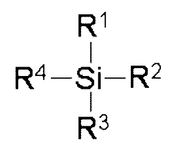
(式中、R1はアルコキシ基またはハロゲン原子であり、R2はアルキル基、シクロアルキル基及びアリール基よりなる群から選択される炭化水素基であるか、一つ以上の水素原子がハロゲン原子で置換されたこれら何れかの炭化水素基であり、R3及びR4はそれぞれ独立にハロゲン原子、またはアルコキシ基、またはアルキル基、シクロアルキル基及びアリール基よりなる群から選択される炭化水素基であるか、一つ以上の水素原子がハロゲン原子で置換されたこれら何れかの炭化水素基である。)
当該シラン化合物はアルコキシ基を少なくとも一つ有していることが必要である。アルコキシ基が存在せずに、アルキル基、シクロアルキル基及びアリール基よりなる群から選択される炭化水素基であるか、一つ以上の水素原子がハロゲン原子で置換されたこれら何れかの炭化水素基のみで置換基が構成される場合、樹脂基材と金属箔の密着性が低下し過ぎる傾向がある。また、当該シラン化合物はアルキル基、シクロアルキル基及びアリール基よりなる群から選択される炭化水素基であるか、一つ以上の水素原子がハロゲン原子で置換されたこれら何れかの炭化水素基を少なくとも一つ有していることが必要である。当該炭化水素基が存在しない場合、樹脂基材と金属箔の密着性が上昇する傾向があるからである。なお、アルコキシ基には一つ以上の水素原子がハロゲン原子に置換されたアルコキシ基も含まれるものとする。
樹脂基材と金属箔の剥離強度を上述した範囲に調節する上では、当該シラン化合物はアルコキシ基を三つ、上記炭化水素基(一つ以上の水素原子がハロゲン原子で置換された炭化水素基を含む)を一つ有していることが好ましい。これを上の式でいえば、R3及びR4の両方がアルコキシ基ということになる。
アルコキシ基としては、限定的ではないが、メトキシ基、エトキシ基、n-又はiso-プロポキシ基、n-、iso-又はtert-ブトキシ基、n-、iso-又はneo-ペントキシ基、n-ヘキソキシ基、シクロヘキシソキシ基、n-ヘプトキシ基、及びn-オクトキシ基等の直鎖状、分岐状、又は環状の炭素数1~20、好ましくは炭素数1~10、より好ましくは炭素数1~5のアルコキシ基が挙げられる。
ハロゲン原子としては、フッ素原子、塩素原子、臭素原子およびヨウ素原子が挙げられる。
ハロゲン原子としては、フッ素原子、塩素原子、臭素原子およびヨウ素原子が挙げられる。
アルキル基としては、限定的ではないが、メチル基、エチル基、n-又はiso-プロピル基、n-、iso-又はtert-ブチル基、n-、iso-又はneo-ペンチル基、n-ヘキシル基、n-オクチル基、n-デシル基等の直鎖状又は分岐状の炭素数1~20、好ましくは炭素数1~10、より好ましくは炭素数1~5のアルキル基が挙げられる。
シクロアルキル基としては、限定的ではないが、シクロプロピル基、シクロブチル基、シクロペンチル基、シクロヘキシル基、シクロへプチル基、シクロオクチル基等の炭素数3~10、好ましくは炭素数5~7のシクロアルキル基が挙げられる。
アリール基としては、フェニル基、アルキル基で置換されたフェニル基(例:トリル基、キシリル基)、1-又は2-ナフチル基、アントリル基等の炭素数6~20、好ましくは6~14のアリール基が挙げられる。
これらの炭化水素基は一つ以上の水素原子がハロゲン原子で置換されてもよく、例えば、フッ素原子、塩素原子、又は臭素原子で置換されることができる。
好ましいシラン化合物の例としては、メチルトリメトキシシラン、エチルトリメトキシシラン、n-又はiso-プロピルトリメトキシシラン、n-、iso-又はtert-ブチルトリメトキシシラン、n-、iso-又はneo-ペンチルトリメトキシシラン、ヘキシルトリメトキシシラン、オクチルトリメトキシシラン、デシルトリメトキシシラン、フェニルトリメトキシシラン;アルキル置換フェニルトリメトキシシラン(例えば、p-(メチル)フェニルトリメトキシシラン)、メチルトリエトキシシラン、エチルトリエトキシシラン、n-又はiso-プロピルトリエトキシシラン、n-、iso-又はtert-ブチルトリエトキシシラン、ペンチルトリエトキシシラン、ヘキシルトリエトキシシラン、オクチルトリエトキシシラン、デシルトリエトキシシラン、フェニルトリエトキシシラン、アルキル置換フェニルトリエトキシシラン(例えば、p-(メチル)フェニルトリエトキシシラン)、(3,3,3-トリフルオロプロピル)トリメトキシシラン、及びトリデカフルオロオクチルトリエトキシシラン、メチルトリクロロシラン、ジメチルジクロロシラン、トリメチルクロロシラン、フェニルトリクロロシラン、トリメチルフルオロシラン、ジメチルジブロモシラン、ジフェニルジブロモシラン、これらの加水分解生成物、及びこれらの加水分解生成物の縮合体などが挙げられる。これらの中でも、入手の容易性の観点から、プロピルトリメトキシシラン、メチルトリエトキシシラン、ヘキシルトリメトキシシラン、フェニルトリエトキシシラン、デシルトリメトキシシランが好ましい。
離型層の形成工程において、シラン化合物は水溶液の形態で使用することができる。水への溶解性を高めるためにメタノールやエタノールなどのアルコールを添加することもできる。アルコールの添加は特に疎水性の高いシラン化合物を使用するときに有効である。シラン化合物の水溶液は、撹拌することでアルコキシ基の加水分解が促進され、撹拌時間が長いと加水分解生成物の縮合が促進される。一般には、十分な撹拌時間を経て加水分解および縮合が進んだシラン化合物を用いた方が樹脂基材と金属箔の剥離強度は低下する傾向にある。従って、撹拌時間の調整によって剥離強度を調整可能である。限定的ではないが、シラン化合物を水に溶解させた後の撹拌時間としては例えば1~100時間とすることができ、典型的には1~30時間とすることができる。当然ながら、撹拌せずに用いる方法もある。
シラン化合物の水溶液中のシラン化合物の濃度は高い方が金属箔と板状キャリアの剥離強度は低下する傾向にあり、シラン化合物の濃度調整によって剥離強度を調整可能である。
また、シラン化合物の水溶液中のシラン化合物の濃度を高くすることで、複数回金属箔を使用しても、従来よりも剥離強度が上昇しにくくなる。シラン化合物の水溶液中のシラン化合物の濃度は、8~15体積%とすることができる。当該濃度が8体積%未満であると、複数回金属箔を使用すると剥離強度が上昇しやすくなる恐れがあり、15体積%超の場合は、シラン化合物の溶解不良が生じ、当該金属箔を樹脂基板と積層させたとき、未反応シラン化合物起因により複数回金属箔を使用すると剥離強度が上昇しやすくなるおそれがある。
また、金属箔(銅箔)の処理表面に、シラン化合物を塗布してから、2回の乾燥工程を実施することが好ましい。1回目の乾燥は、シラン化合物の溶液を乾かすだけの目的で行う。2回目の乾燥は、縮合反応しきっていないシラン化合物内の水酸基について、縮合反応を全部終わらせて、残存しているOH基(水酸基)を無くすことで、シラン化合物により形成された離型層がより強固となり、複数回金属箔を使用した場合に剥離強度が上昇しにくいという効果がある。1回目の乾燥は、80~120℃×10秒~2分間で行うことができ、2回目の乾燥は、120~200℃×30秒~5分間で行うことができる。
また、シラン化合物の水-アルコ-ル混合溶液を用いる場合、当該溶液中のアルコール濃度は、水に溶けにくいシラン化合物を均一に溶解させるため、20~80体積%が好ましい。当該溶液中のアルコール濃度が20体積%未満であると、シラン化合物が溶けなくなる場合があり、80体積%超の場合、加水分解反応が不完全となるため、シラン化合物が加水分解されずにそのまま残存し、離型層が脆弱となり、複数回金属箔を使用すると剥離強度が上昇しやすくなる恐れがある。
また、シラン化合物の水溶液中のシラン化合物の濃度を高くすることで、複数回金属箔を使用しても、従来よりも剥離強度が上昇しにくくなる。シラン化合物の水溶液中のシラン化合物の濃度は、8~15体積%とすることができる。当該濃度が8体積%未満であると、複数回金属箔を使用すると剥離強度が上昇しやすくなる恐れがあり、15体積%超の場合は、シラン化合物の溶解不良が生じ、当該金属箔を樹脂基板と積層させたとき、未反応シラン化合物起因により複数回金属箔を使用すると剥離強度が上昇しやすくなるおそれがある。
また、金属箔(銅箔)の処理表面に、シラン化合物を塗布してから、2回の乾燥工程を実施することが好ましい。1回目の乾燥は、シラン化合物の溶液を乾かすだけの目的で行う。2回目の乾燥は、縮合反応しきっていないシラン化合物内の水酸基について、縮合反応を全部終わらせて、残存しているOH基(水酸基)を無くすことで、シラン化合物により形成された離型層がより強固となり、複数回金属箔を使用した場合に剥離強度が上昇しにくいという効果がある。1回目の乾燥は、80~120℃×10秒~2分間で行うことができ、2回目の乾燥は、120~200℃×30秒~5分間で行うことができる。
また、シラン化合物の水-アルコ-ル混合溶液を用いる場合、当該溶液中のアルコール濃度は、水に溶けにくいシラン化合物を均一に溶解させるため、20~80体積%が好ましい。当該溶液中のアルコール濃度が20体積%未満であると、シラン化合物が溶けなくなる場合があり、80体積%超の場合、加水分解反応が不完全となるため、シラン化合物が加水分解されずにそのまま残存し、離型層が脆弱となり、複数回金属箔を使用すると剥離強度が上昇しやすくなる恐れがある。
シラン化合物の水溶液のpHは特に制限はなく、酸性側でもアルカリ性側でも利用できる。例えば3.0~10.0の範囲のpHで使用できる。特段のpH調整が不要であるという観点から中性付近である5.0~9.0の範囲のpHとするのが好ましく、7.0~9.0の範囲のpHとするのがより好ましい。
(2)分子内に2つ以下のメルカプト基を有する化合物
離型層は、分子内に2つ以上のメルカプト基を有する化合物を用いて構成し、当該離型層を介して樹脂基材と金属箔とを貼り合わせることによっても、適度に密着性が低下し、剥離強度を調節できる。
但し、分子内に3つ以上のメルカプト基を有する化合物またはその塩を樹脂基材と金属箔との間に介在させて貼り合わせた場合、剥離強度低減の目的には適さない。これは、分子内にメルカプト基が過剰に存在するとメルカプト基同士、またはメルカプト基と板状キャリア、またはメルカプト基と金属箔との化学反応によってスルフィド結合、ジスルフィド結合またはポリスルフィド結合が過剰に生成し、樹脂基材と金属箔の間に強固な3次元架橋構造が形成されることで剥離強度が上昇することがあると考えられるからである。このような事例は特開2000-196207号公報に開示されている。
離型層は、分子内に2つ以上のメルカプト基を有する化合物を用いて構成し、当該離型層を介して樹脂基材と金属箔とを貼り合わせることによっても、適度に密着性が低下し、剥離強度を調節できる。
但し、分子内に3つ以上のメルカプト基を有する化合物またはその塩を樹脂基材と金属箔との間に介在させて貼り合わせた場合、剥離強度低減の目的には適さない。これは、分子内にメルカプト基が過剰に存在するとメルカプト基同士、またはメルカプト基と板状キャリア、またはメルカプト基と金属箔との化学反応によってスルフィド結合、ジスルフィド結合またはポリスルフィド結合が過剰に生成し、樹脂基材と金属箔の間に強固な3次元架橋構造が形成されることで剥離強度が上昇することがあると考えられるからである。このような事例は特開2000-196207号公報に開示されている。
この分子内に2つ以下のメルカプト基を有する化合物としては、チオール、ジチオール、チオカルボン酸またはその塩、ジチオカルボン酸またはその塩、チオスルホン酸またはその塩、およびジチオスルホン酸またはその塩が挙げられ、これらの中から選択される少なくとも一種を用いることができる。
チオールは、分子内に一つのメルカプト基を有するものであり、例えばR-SHで表される。ここで、Rは、水酸基またはアミノ基を含んでもよい、脂肪族系または芳香族系炭化水素基または複素環基を表す。
ジチオールは、分子内に二つのメルカプト基を有するものであり、例えばR(SH)2で表される。Rは、水酸基またはアミノ基を含んでもよい、脂肪族系または芳香族系炭化水素基または複素環基を表す。また、二つのメルカプト基は、それぞれ同じ炭素に結合してもよいし、互いに別々の炭素または窒素に結合してもよい。
チオカルボン酸は、有機カルボン酸の水酸基がメルカプト基に置換されたものであり、例えばR-CO-SHで表される。Rは、水酸基またはアミノ基を含んでもよい、脂肪族系または芳香族系炭化水素基または複素環基を表す。また、チオカルボン酸は、塩の形態でも使用することが可能である。なお、チオカルボン酸基を、二つ有する化合物も使用可能である。
ジチオカルボン酸は、有機カルボン酸のカルボキシ基中の2つの酸素原子が硫黄原子に置換されたものであり、例えばR-(CS)-SHで表される。Rは、水酸基またはアミノ基を含んでもよい、脂肪族系または芳香族系炭化水素基または複素環基を表す。また、ジチオカルボン酸は、塩の形態でも使用することが可能である。なお、ジチオカルボン酸基を、二つ有する化合物も使用可能である。
チオスルホン酸は、有機スルホン酸の水酸基がメルカプト基に置換されたものであり、例えばR(SO2)-SHで表される。Rは、水酸基またはアミノ基を含んでもよい、脂肪族系または芳香族系炭化水素基または複素環基を表す。また、チオスルホン酸は、塩の形態でも使用することが可能である。
ジチオスルホン酸は、有機ジスルホン酸の二つの水酸基がそれぞれメルカプト基に置換されたものであり、例えばR-((SO2)-SH)2で表される。Rは、水酸基またはアミノ基を含んでもよい、脂肪族系または芳香族系炭化水素基または複素環基を表す。また、二つのチオスルホン酸基は、それぞれ同じ炭素に結合してもよいし、互いに別々の炭素に結合してもよい。また、ジチオスルホン酸は、塩の形態でも使用することが可能である。
ここで、Rとして好適な脂肪族系炭化水素基としては、アルキル基、シクロアルキル基が挙げられ、これら炭化水素基は水酸基とアミノ基のどちらかまたは両方を含んでいてもよい。
また、アルキル基としては、限定的ではないが、メチル基、エチル基、n-又はiso-プロピル基、n-、iso-又はtert-ブチル基、n-、iso-又はneo-ペンチル基、n-ヘキシル基、n-オクチル基、n-デシル基等の直鎖状又は分岐状の炭素数1~20、好ましくは炭素数1~10、より好ましくは炭素数1~5のアルキル基が挙げられる。
また、シクロアルキル基としては、限定的ではないが、シクロプロピル基、シクロブチル基、シクロペンチル基、シクロヘキシル基、シクロへプチル基、シクロオクチル基等の炭素数3~10、好ましくは炭素数5~7のシクロアルキル基が挙げられる。
また、Rとして好適な芳香族炭化水素基としては、フェニル基、アルキル基で置換されたフェニル基(例:トリル基、キシリル基)、1-又は2-ナフチル基、アントリル基等の炭素数6~20、好ましくは6~14のアリール基が挙げられ、これら炭化水素基は水酸基とアミノ基のどちらかまたは両方を含んでいてもよい。
また、Rとして好適な複素環基としては、イミダゾール、トリアゾール、テトラゾール、ベンゾイミダゾール、ベンゾトリアゾール、チアゾール、ベンゾチアゾールが挙げられ、水酸基とアミノ基のどちらかまたは両方を含んでいてもよい。
分子内に2つ以下のメルカプト基を有する化合物の好ましい例としては、3-メルカプト-1,2プロパンジオール、2-メルカプトエタノール、1,2-エタンジチオール、6-メルカプト-1-ヘキサノール、1-オクタンチオール、1-ドデカンチオール、10-ヒドロキシ-1-ドデカンチオール、10-カルボキシ-1-ドデカンチオール、10-アミノ-1-ドデカンチオール、1-ドデカンチオールスルホン酸ナトリウム、チオフェノール、チオ安息香酸、4-アミノ-チオフェノール、p-トルエンチオール、2,4-ジメチルベンゼンチオール、3-メルカプト-1,2,4トリアゾール、2-メルカプト-ベンゾチアゾールが挙げられる。これらの中でも水溶性と廃棄物処理上の観点から、3-メルカプト-1,2プロパンジオールが好ましい。
離型層の形成工程において、分子内に2つ以下のメルカプト基を有する化合物は水溶液の形態で使用することができる。水への溶解性を高めるためにメタノールやエタノールなどのアルコールを添加することもできる。アルコールの添加は特に疎水性の高い分子内に2つ以下のメルカプト基を有する化合物を使用するときに有効である。
分子内に2つ以下のメルカプト基を有する化合物の水溶液中の濃度は高い方が樹脂基材と金属箔の剥離強度は低下する傾向にあり、分子内に2つ以下のメルカプト基を有する化合物の濃度調整によって剥離強度を調整可能である
また、分子内に2つ以下のメルカプト基を有する化合物の水溶液中の濃度を高くすることで、複数回金属箔を使用しても、従来よりも剥離強度が上昇しにくくなる。分子内に2つ以下のメルカプト基を有する化合物の水溶液中の濃度は、8~15体積%とすることができる。当該濃度が8体積%未満であると、複数回金属箔を使用すると剥離強度が上昇しやすくなる恐れがあり、15体積%超の場合は、分子内に2つ以下のメルカプト基を有する化合物の溶解不良が生じ、当該金属箔を樹脂基板と積層させたとき、溶解していない分子内に2つ以下のメルカプト基を有する化合物起因により複数回金属箔を使用すると剥離強度が上昇しやすくなるおそれがある。
また、金属箔(銅箔)の処理表面に、分子内に2つ以下のメルカプト基を有する化合物を塗布してから、2回の乾燥工程を実施することが好ましい。1回目の乾燥は、分子内に2つ以下のメルカプト基を有する化合物の溶液を乾かすだけの目的で行う。2回目の乾燥は、2回目の乾燥は、金属箔表面に配位した分子内に2つ以下のメルカプト基を有する化合物の配列を調整することにより、分子内に2つ以下のメルカプト基を有する化合物により形成された離型層がより強固となり、複数回金属箔を使用した場合に剥離強度が上昇しにくいという効果がある。1回目の乾燥は、80~120℃×10秒~2分間で行うことができ、2回目の乾燥は、120~200℃×30秒~5分間で行うことができる。
また、分子内に2つ以下のメルカプト基を有する化合物の水-アルコ-ル混合溶液を用いる場合、当該溶液中のアルコール濃度は、水に溶けにくい分子内に2つ以下のメルカプト基を有する化合物を均一に溶解させるため、20~80体積%が好ましい。当該溶液中のアルコール濃度が20体積%未満であると、分子内に2つ以下のメルカプト基を有する化合物が溶けなくなって離型層が脆弱となる場合があり、80体積%超の場合、金属箔表面に緻密に配位した分子内に2つ以下のメルカプト基を有する化合物の配列が乱れ、離型層が脆弱となり、複数回金属箔を使用すると剥離強度が上昇しやすくなる恐れがある。
また、分子内に2つ以下のメルカプト基を有する化合物の水溶液中の濃度を高くすることで、複数回金属箔を使用しても、従来よりも剥離強度が上昇しにくくなる。分子内に2つ以下のメルカプト基を有する化合物の水溶液中の濃度は、8~15体積%とすることができる。当該濃度が8体積%未満であると、複数回金属箔を使用すると剥離強度が上昇しやすくなる恐れがあり、15体積%超の場合は、分子内に2つ以下のメルカプト基を有する化合物の溶解不良が生じ、当該金属箔を樹脂基板と積層させたとき、溶解していない分子内に2つ以下のメルカプト基を有する化合物起因により複数回金属箔を使用すると剥離強度が上昇しやすくなるおそれがある。
また、金属箔(銅箔)の処理表面に、分子内に2つ以下のメルカプト基を有する化合物を塗布してから、2回の乾燥工程を実施することが好ましい。1回目の乾燥は、分子内に2つ以下のメルカプト基を有する化合物の溶液を乾かすだけの目的で行う。2回目の乾燥は、2回目の乾燥は、金属箔表面に配位した分子内に2つ以下のメルカプト基を有する化合物の配列を調整することにより、分子内に2つ以下のメルカプト基を有する化合物により形成された離型層がより強固となり、複数回金属箔を使用した場合に剥離強度が上昇しにくいという効果がある。1回目の乾燥は、80~120℃×10秒~2分間で行うことができ、2回目の乾燥は、120~200℃×30秒~5分間で行うことができる。
また、分子内に2つ以下のメルカプト基を有する化合物の水-アルコ-ル混合溶液を用いる場合、当該溶液中のアルコール濃度は、水に溶けにくい分子内に2つ以下のメルカプト基を有する化合物を均一に溶解させるため、20~80体積%が好ましい。当該溶液中のアルコール濃度が20体積%未満であると、分子内に2つ以下のメルカプト基を有する化合物が溶けなくなって離型層が脆弱となる場合があり、80体積%超の場合、金属箔表面に緻密に配位した分子内に2つ以下のメルカプト基を有する化合物の配列が乱れ、離型層が脆弱となり、複数回金属箔を使用すると剥離強度が上昇しやすくなる恐れがある。
分子内に2つ以下のメルカプト基を有する化合物の水溶液のpHは特に制限はなく、酸性側でもアルカリ性側でも利用できる。例えば3.0~10.0の範囲のpHで使用できる。特段のpH調整が不要であるという観点から中性付近である5.0~9.0の範囲のpHとするのが好ましく、7.0~9.0の範囲のpHとするのがより好ましい。
(3)金属アルコキシド
離型層を、次式に示す構造を有するアルミネート化合物、チタネート化合物、ジルコネート化合物、またはその加水分解生成物、または該加水分解生成物の縮合体(以下、単に金属アルコキシドと記述する)を単独でまたは複数混合して構成してもよい。当該離型層を介して樹脂基材と金属箔を貼り合わせることで、適度に密着性が低下し、剥離強度を調節できる。
離型層を、次式に示す構造を有するアルミネート化合物、チタネート化合物、ジルコネート化合物、またはその加水分解生成物、または該加水分解生成物の縮合体(以下、単に金属アルコキシドと記述する)を単独でまたは複数混合して構成してもよい。当該離型層を介して樹脂基材と金属箔を貼り合わせることで、適度に密着性が低下し、剥離強度を調節できる。

式中、R1はアルコキシ基またはハロゲン原子であり、R2はアルキル基、シクロアルキル基及びアリール基よりなる群から選択される炭化水素基であるか、一つ以上の水素原子がハロゲン原子で置換されたこれら何れかの炭化水素基であり、MはAl、Ti、Zrのうちいずれか一つ、nは0または1または2、mは1以上Mの価数以下の整数であり、R1の少なくとも一つはアルコキシ基である。なお、m+nはMの価数すなわちAlの場合3、Ti、Zrの場合4である。
当該金属アルコキシドはアルコキシ基を少なくとも一つ有していることが必要である。アルコキシ基が存在せずに、アルキル基、シクロアルキル基及びアリール基よりなる群から選択される炭化水素基であるか、一つ以上の水素原子がハロゲン原子で置換されたこれら何れかの炭化水素基のみで置換基が構成される場合、樹脂基材と金属箔の密着性が低下し過ぎる傾向がある。また、当該金属アルコキシドはアルキル基、シクロアルキル基及びアリール基よりなる群から選択される炭化水素基であるか、一つ以上の水素原子がハロゲン原子で置換されたこれら何れかの炭化水素基を0~2個有していることが必要である。当該炭化水素基を3つ以上有する場合、樹脂基材と金属箔の密着性が低下し過ぎる傾向があるからである。なお、アルコキシ基には一つ以上の水素原子がハロゲン原子に置換されたアルコキシ基も含まれるものとする。樹脂基材と金属箔の剥離強度を上述した範囲に調節する上では、当該金属アルコキシドはアルコキシ基を二つ以上、上記炭化水素基(一つ以上の水素原子がハロゲン原子で置換された炭化水素基を含む)を一つか二つ有していることが好ましい。
また、アルキル基としては、限定的ではないが、メチル基、エチル基、n-又はiso-プロピル基、n-、iso-又はtert-ブチル基、n-、iso-又はneo-ペンチル基、n-ヘキシル基、n-オクチル基、n-デシル基等の直鎖状又は分岐状の炭素数1~20、好ましくは炭素数1~10、より好ましくは炭素数1~5のアルキル基が挙げられる。
また、シクロアルキル基としては、限定的ではないが、シクロプロピル基、シクロブチル基、シクロペンチル基、シクロヘキシル基、シクロへプチル基、シクロオクチル基等の炭素数3~10、好ましくは炭素数5~7のシクロアルキル基が挙げられる。
また、R2として好適な芳香族炭化水素基としては、フェニル基、アルキル基で置換されたフェニル基(例:トリル基、キシリル基)、1-又は2-ナフチル基、アントリル基等の炭素数6~20、好ましくは6~14のアリール基が挙げられ、これら炭化水素基は水酸基とアミノ基のどちらかまたは両方を含んでいてもよい。これらの炭化水素基は一つ以上の水素原子がハロゲン原子で置換されてもよく、例えば、フッ素原子、塩素原子、又は臭素原子で置換されることができる。
好ましいアルミネート化合物の例としては、トリメトキシアルミニウム、メチルジメトキシアルミニウム、エチルジメトキシアルミニウム、n-又はiso-プロピルジメトキシアルミニウム、n-、iso-又はtert-ブチルジメトキシアルミニウム、n-、iso-又はneo-ペンチルジメトキシアルミニウム、ヘキシルジメトキシアルミニウム、オクチルジメトキシアルミニウム、デシルジメトキシアルミニウム、フェニルジメトキシアルミニウム;アルキル置換フェニルジメトキシアルミニウム(例えば、p-(メチル)フェニルジメトキシアルミニウム)、ジメチルメトキシアルミニウム、トリエトキシアルミニウム、メチルジエトキシアルミニウム、エチルジエトキシアルミニウム、n-又はiso-プロピルジエトキシアルミニウム、n-、iso-又はtert-ブチルジエトキシアルミニウム、ペンチルジエトキシアルミニウム、ヘキシルジエトキシアルミニウム、オクチルジエトキシアルミニウム、デシルジエトキシアルミニウム、フェニルジエトキシアルミニウム、アルキル置換フェニルジエトキシアルミニウム(例えば、p-(メチル)フェニルジエトキシアルミニウム)、ジメチルエトキシアルミニウム、トリイソプロポキシアルミニウム、メチルジイソプロポキシアルミニウム、エチルジイソプロポキシアルミニウム、n-又はiso-プロピルジエトキシアルミニウム、n-、iso-又はtert-ブチルジイソプロポキシアルミニウム、ペンチルジイソプロポキシアルミニウム、ヘキシルジイソプロポキシアルミニウム、オクチルジイソプロポキシアルミニウム、デシルジイソプロポキシアルミニウム、フェニルジイソプロポキシアルミニウム、アルキル置換フェニルジイソプロポキシアルミニウム(例えば、p-(メチル)フェニルジイソプロポキシアルミニウム)、ジメチルイソプロポキシアルミニウム、(3,3,3-トリフルオロプロピル)ジメトキシアルミニウム、及びトリデカフルオロオクチルジエトキシアルミニウム、メチルジクロロアルミニウム、ジメチルクロロアルミニウム、ジメチルクロロアルミニウム、フェニルジクロロアルミニウム、ジメチルフルオロアルミニウム、ジメチルブロモアルミニウム、ジフェニルブロモアルミニウム、これらの加水分解生成物、及びこれらの加水分解生成物の縮合体などが挙げられる。これらの中でも、入手の容易性の観点から、トリメトキシアルミニウム、トリエトキシアルミニウム、トリイソプロポキシアルミニウム、が好ましい。
好ましいチタネート化合物の例としては、テトラメトキシチタン、メチルトリメトキシチタン、エチルトリメトキシチタン、n-又はiso-プロピルトリメトキシチタン、n-、iso-又はtert-ブチルトリメトキシチタン、n-、iso-又はneo-ペンチルトリメトキシチタン、ヘキシルトリメトキシチタン、オクチルトリメトキシチタン、デシルトリメトキシチタン、フェニルトリメトキシチタン;アルキル置換フェニルトリメトキシチタン(例えば、p-(メチル)フェニルトリメトキシチタン)、ジメチルジメトキシチタン、テトラエトキシチタン、メチルトリエトキシチタン、エチルトリエトキシチタン、n-又はiso-プロピルトリエトキシチタン、n-、iso-又はtert-ブチルトリエトキシチタン、ペンチルトリエトキシチタン、ヘキシルトリエトキシチタン、オクチルトリエトキシチタン、デシルトリエトキシチタン、フェニルトリエトキシチタン、アルキル置換フェニルトリエトキシチタン(例えば、p-(メチル)フェニルトリエトキシチタン)、ジメチルジエトキシチタン、テトライソプロポキシチタン、メチルトリイソプロポキシチタン、エチルトリイソプロポキシチタン、n-又はiso-プロピルトリエトキシチタン、n-、iso-又はtert-ブチルトリイソプロポキシチタン、ペンチルトリイソプロポキシチタン、ヘキシルトリイソプロポキシチタン、オクチルトリイソプロポキシチタン、デシルトリイソプロポキシチタン、フェニルトリイソプロポキシチタン、アルキル置換フェニルトリイソプロポキシチタン(例えば、p-(メチル)フェニルトリイソプロポキシチタン)、ジメチルジイソプロポキシチタン、(3,3,3-トリフルオロプロピル)トリメトキシチタン、及びトリデカフルオロオクチルトリエトキシチタン、メチルトリクロロチタン、ジメチルジクロロチタン、トリメチルクロロチタン、フェニルトリクロロチタン、ジメチルジフルオロチタン、ジメチルジブロモチタン、ジフェニルジブロモチタン、これらの加水分解生成物、及びこれらの加水分解生成物の縮合体などが挙げられる。これらの中でも、入手の容易性の観点から、テトラメトキシチタン、テトラエトキシチタン、テトライソプロポキシチタン、が好ましい。
好ましいジルコネート化合物の例としては、テトラメトキシジルコニウム、メチルトリメトキシジルコニウム、エチルトリメトキシジルコニウム、n-又はiso-プロピルトリメトキシジルコニウム、n-、iso-又はtert-ブチルトリメトキシジルコニウム、n-、iso-又はneo-ペンチルトリメトキシジルコニウム、ヘキシルトリメトキシジルコニウム、オクチルトリメトキシジルコニウム、デシルトリメトキシジルコニウム、フェニルトリメトキシジルコニウム;アルキル置換フェニルトリメトキシジルコニウム(例えば、p-(メチル)フェニルトリメトキシジルコニウム)、ジメチルジメトキシジルコニウム、テトラエトキシジルコニウム、メチルトリエトキシジルコニウム、エチルトリエトキシジルコニウム、n-又はiso-プロピルトリエトキシジルコニウム、n-、iso-又はtert-ブチルトリエトキシジルコニウム、ペンチルトリエトキシジルコニウム、ヘキシルトリエトキシジルコニウム、オクチルトリエトキシジルコニウム、デシルトリエトキシジルコニウム、フェニルトリエトキシジルコニウム、アルキル置換フェニルトリエトキシジルコニウム(例えば、p-(メチル)フェニルトリエトキシジルコニウム)、ジメチルジエトキシジルコニウム、テトライソプロポキシジルコニウム、メチルトリイソプロポキシジルコニウム、エチルトリイソプロポキシジルコニウム、n-又はiso-プロピルトリエトキシジルコニウム、n-、iso-又はtert-ブチルトリイソプロポキシジルコニウム、ペンチルトリイソプロポキシジルコニウム、ヘキシルトリイソプロポキシジルコニウム、オクチルトリイソプロポキシジルコニウム、デシルトリイソプロポキシジルコニウム、フェニルトリイソプロポキシジルコニウム、アルキル置換フェニルトリイソプロポキシジルコニウム(例えば、p-(メチル)フェニルトリイソプロポキシチタン)、ジメチルジイソプロポキシジルコニウム、(3,3,3-トリフルオロプロピル)トリメトキシジルコニウム、及びトリデカフルオロオクチルトリエトキシジルコニウム、メチルトリクロロジルコニウム、ジメチルジクロロジルコニウム、トリメチルクロロジルコニウム、フェニルトリクロロジルコニウム、ジメチルジフルオロジルコニウム、ジメチルジブロモジルコニウム、ジフェニルジブロモジルコニウム、これらの加水分解生成物、及びこれらの加水分解生成物の縮合体などが挙げられる。これらの中でも、入手の容易性の観点から、テトラメトキシジルコニウム、テトラエトキシジルコニウム、テトライソプロポキシジルコニウム、が好ましい。
離型層の形成工程において、金属アルコキシドは水溶液の形態で使用することができる。水への溶解性を高めるためにメタノールやエタノールなどのアルコールを添加することもできる。アルコールの添加は特に疎水性の高い金属アルコキシドを使用するときに有効である。
金属アルコキシドの水溶液中の濃度は高い方が樹脂基材と金属箔の剥離強度は低下する傾向にあり、金属アルコキシド濃度調整によって剥離強度を調整可能である。
また、金属アルコキシドの水溶液中の濃度を高くすることで、複数回金属箔を使用しても、従来よりも剥離強度が上昇しにくくなる。金属アルコキシドの水溶液中の濃度は、8~15体積%とすることができる。当該濃度が8体積%未満であると、複数回金属箔を使用すると剥離強度が上昇しやすくなる恐れがあり、15体積%超の場合は、金属アルコキシドの溶解不良が生じ、当該金属箔を樹脂基板と積層させたとき、未反応化合物起因により複数回金属箔を使用すると剥離強度が上昇しやすくなるおそれがある。
また、金属箔(銅箔)の処理表面に、金属アルコキシドを塗布してから、2回の乾燥工程を実施することが好ましい。1回目の乾燥は、金属アルコキシドの溶液を乾かすだけの目的で行う。2回目の乾燥は、縮合反応しきっていない金属アルコキシド内の水酸基について、縮合反応を全部終わらせて、残存しているOH基(水酸基)を無くすことで、金属アルコキシドにより形成された離型層がより強固となり、複数回金属箔を使用した場合に剥離強度が上昇しにくいという効果がある。1回目の乾燥は、80~120℃×10秒~2分間で行うことができ、2回目の乾燥は、120~200℃×30秒~5分間で行うことができる。
また、金属アルコキシドの水-アルコ-ル混合溶液を用いる場合、当該溶液中のアルコール濃度は、水に溶けにくい金属アルコキシドを均一に溶解させるため、20~80体積%が好ましい。当該溶液中のアルコール濃度が20体積%未満であると、金属アルコキシドが溶けなくなる場合があり、80体積%超の場合、加水分解反応が不完全となるため、金属アルコキシドが加水分解されずにそのまま残存し、離型層が脆弱となり、複数回金属箔を使用すると剥離強度が上昇しやすくなる恐れがある。
また、金属アルコキシドの水溶液中の濃度を高くすることで、複数回金属箔を使用しても、従来よりも剥離強度が上昇しにくくなる。金属アルコキシドの水溶液中の濃度は、8~15体積%とすることができる。当該濃度が8体積%未満であると、複数回金属箔を使用すると剥離強度が上昇しやすくなる恐れがあり、15体積%超の場合は、金属アルコキシドの溶解不良が生じ、当該金属箔を樹脂基板と積層させたとき、未反応化合物起因により複数回金属箔を使用すると剥離強度が上昇しやすくなるおそれがある。
また、金属箔(銅箔)の処理表面に、金属アルコキシドを塗布してから、2回の乾燥工程を実施することが好ましい。1回目の乾燥は、金属アルコキシドの溶液を乾かすだけの目的で行う。2回目の乾燥は、縮合反応しきっていない金属アルコキシド内の水酸基について、縮合反応を全部終わらせて、残存しているOH基(水酸基)を無くすことで、金属アルコキシドにより形成された離型層がより強固となり、複数回金属箔を使用した場合に剥離強度が上昇しにくいという効果がある。1回目の乾燥は、80~120℃×10秒~2分間で行うことができ、2回目の乾燥は、120~200℃×30秒~5分間で行うことができる。
また、金属アルコキシドの水-アルコ-ル混合溶液を用いる場合、当該溶液中のアルコール濃度は、水に溶けにくい金属アルコキシドを均一に溶解させるため、20~80体積%が好ましい。当該溶液中のアルコール濃度が20体積%未満であると、金属アルコキシドが溶けなくなる場合があり、80体積%超の場合、加水分解反応が不完全となるため、金属アルコキシドが加水分解されずにそのまま残存し、離型層が脆弱となり、複数回金属箔を使用すると剥離強度が上昇しやすくなる恐れがある。
金属アルコキシドの水溶液のpHは特に制限はなく、酸性側でもアルカリ性側でも利用できる。例えば3.0~10.0の範囲のpHで使用できる。特段のpH調整が不要であるという観点から中性付近である5.0~9.0の範囲のpHとするのが好ましく、7.0~9.0の範囲のpHとするのがより好ましい。
(4)その他
シリコン系の離型剤、離型性を有する樹脂被膜等、公知の離型性を有する物質を離型層に用いることができる。
(4)その他
シリコン系の離型剤、離型性を有する樹脂被膜等、公知の離型性を有する物質を離型層に用いることができる。
本発明に係る金属箔は、粗化処理層、耐熱層、防錆層、クロメート処理層及びシランカップリング処理層からなる群から選択された1種以上の層が設けられていてもよい。ここでクロメート処理層とは無水クロム酸、クロム酸、二クロム酸、クロム酸塩または二クロム酸塩を含む液で処理された層のことをいう。クロメート処理層はコバルト、鉄、ニッケル、モリブデン、亜鉛、タンタル、銅、アルミニウム、リン、タングステン、錫、砒素およびチタン等の元素(金属、合金、酸化物、窒化物、硫化物等どのような形態でもよい)を含んでもよい。クロメート処理層の具体例としては、無水クロム酸または二クロム酸カリウム水溶液で処理したクロメート処理層や、無水クロム酸または二クロム酸カリウムおよび亜鉛を含む処理液で処理したクロメート処理層等が挙げられる。
粗化処理層は例えば以下の処理により形成することができる。
〔球状粗化〕
Cu、H2SO4、Asから成る、以下に記す銅粗化めっき浴を用いて球状粗化粒子を形成する。
・液組成1
CuSO4・5H2O 78~196g/L
Cu 20~50g/L
H2SO4 50~200g/L
砒素 0.7~3.0g/L
(電気メッキ温度1) 30~76℃
(電流条件1) 電流密度 35~105A/dm2 (浴の限界電流密度以上)
(メッキ時間1)1~240秒
続いて、粗化粒子の脱落防止とピール強度向上のため、硫酸・硫酸銅からなる銅電解浴で被せメッキを行う。被せメッキ条件を以下に記す。
・液組成2
CuSO4・5H2O 88~352g/L
Cu 22~90g/L
H2SO4 50~200g/L
(電気メッキ温度2) 25~80℃
(電流条件2) 電流密度:15~32A/dm2 (浴の限界電流密度未満)
(メッキ時間1)1~240秒
〔球状粗化〕
Cu、H2SO4、Asから成る、以下に記す銅粗化めっき浴を用いて球状粗化粒子を形成する。
・液組成1
CuSO4・5H2O 78~196g/L
Cu 20~50g/L
H2SO4 50~200g/L
砒素 0.7~3.0g/L
(電気メッキ温度1) 30~76℃
(電流条件1) 電流密度 35~105A/dm2 (浴の限界電流密度以上)
(メッキ時間1)1~240秒
続いて、粗化粒子の脱落防止とピール強度向上のため、硫酸・硫酸銅からなる銅電解浴で被せメッキを行う。被せメッキ条件を以下に記す。
・液組成2
CuSO4・5H2O 88~352g/L
Cu 22~90g/L
H2SO4 50~200g/L
(電気メッキ温度2) 25~80℃
(電流条件2) 電流密度:15~32A/dm2 (浴の限界電流密度未満)
(メッキ時間1)1~240秒
また、耐熱層、防錆層としては公知の耐熱層、防錆層を用いることができる。例えば、耐熱層および/または防錆層はニッケル、亜鉛、錫、コバルト、モリブデン、銅、タングステン、リン、ヒ素、クロム、バナジウム、チタン、アルミニウム、金、銀、白金族元素、鉄、タンタルの群から選ばれる1種以上の元素を含む層であってもよく、ニッケル、亜鉛、錫、コバルト、モリブデン、銅、タングステン、リン、ヒ素、クロム、バナジウム、チタン、アルミニウム、金、銀、白金族元素、鉄、タンタルの群から選ばれる1種以上の元素からなる金属層または合金層であってもよい。また、耐熱層および/または防錆層はニッケル、亜鉛、錫、コバルト、モリブデン、銅、タングステン、リン、ヒ素、クロム、バナジウム、チタン、アルミニウム、金、銀、白金族元素、鉄、タンタルの群から選ばれる1種以上の元素を含む酸化物、窒化物、珪化物を含んでもよい。また、耐熱層および/または防錆層はニッケル-亜鉛合金を含む層であってもよい。また、耐熱層および/または防錆層はニッケル-亜鉛合金層であってもよい。前記ニッケル-亜鉛合金層は、不可避不純物を除き、ニッケルを50wt%~99wt%、亜鉛を50wt%~1wt%含有するものであってもよい。前記ニッケル-亜鉛合金層の亜鉛及びニッケルの合計付着量が5~1000mg/m2、好ましくは10~500mg/m2、好ましくは20~100mg/m2であってもよい。また、前記ニッケル-亜鉛合金を含む層または前記ニッケル-亜鉛合金層のニッケルの付着量と亜鉛の付着量との比(=ニッケルの付着量/亜鉛の付着量)が1.5~10であることが好ましい。また、前記ニッケル-亜鉛合金を含む層または前記ニッケル-亜鉛合金層のニッケルの付着量は0.5mg/m2~500mg/m2であることが好ましく、1mg/m2~50mg/m2であることがより好ましい。
例えば耐熱層および/または防錆層は、付着量が1mg/m2~100mg/m2、好ましくは5mg/m2~50mg/m2のニッケルまたはニッケル合金層と、付着量が1mg/m2~80mg/m2、好ましくは5mg/m2~40mg/m2のスズ層とを順次積層したものであってもよく、前記ニッケル合金層はニッケル-モリブデン、ニッケル-亜鉛、ニッケル-モリブデン-コバルトのいずれか一種により構成されてもよい。また、耐熱層および/または防錆層は、ニッケルまたはニッケル合金とスズとの合計付着量が2mg/m2~150mg/m2であることが好ましく、10mg/m2~70mg/m2であることがより好ましい。また、耐熱層および/または防錆層は、[ニッケルまたはニッケル合金中のニッケル付着量]/[スズ付着量]=0.25~10であることが好ましく、0.33~3であることがより好ましい。
なお、シランカップリング処理に用いられるシランカップリング剤には公知のシランカップリング剤を用いてよく、例えばアミノ系シランカップリング剤又はエポキシ系シランカップリング剤、メルカプト系シランカップリング剤を用いてよい。また、シランカップリング剤にはビニルトリメトキシシラン、ビニルフェニルトリメトキシラン、γ‐メタクリロキシプロピルトリメトキシシラン、γ‐グリシドキシプロピルトリメトキシシラン、4‐グリシジルブチルトリメトキシシラン、γ‐アミノプロピルトリエトキシシラン、N‐β(アミノエチル)γ‐アミノプロピルトリメトキシシラン、N‐3‐(4‐(3‐アミノプロポキシ)プトキシ)プロピル‐3‐アミノプロピルトリメトキシシラン、イミダゾールシラン、トリアジンシラン、γ‐メルカプトプロピルトリメトキシシラン等を用いてもよい。
前記シランカップリング処理層は、エポキシ系シラン、アミノ系シラン、メタクリロキシ系シラン、メルカプト系シランなどのシランカップリング剤などを使用して形成してもよい。なお、このようなシランカップリング剤は、2種以上混合して使用してもよい。中でも、アミノ系シランカップリング剤又はエポキシ系シランカップリング剤を用いて形成したものであることが好ましい。
ここで言うアミノ系シランカップリング剤とは、N‐(2‐アミノエチル)‐3‐アミノプロピルトリメトキシシラン、3‐(N‐スチリルメチル‐2‐アミノエチルアミノ)プロピルトリメトキシシラン、3‐アミノプロピルトリエトキシシラン、ビス(2‐ヒドロキシエチル)‐3‐アミノプロピルトリエトキシシラン、アミノプロピルトリメトキシシラン、N‐メチルアミノプロピルトリメトキシシラン、N‐フェニルアミノプロピルトリメトキシシラン、N‐(3‐アクリルオキシ‐2‐ヒドロキシプロピル)‐3‐アミノプロピルトリエトキシシラン、4‐アミノブチルトリエトキシシラン、(アミノエチルアミノメチル)フェネチルトリメトキシシラン、N‐(2‐アミノエチル‐3‐アミノプロピル)トリメトキシシラン、N‐(2‐アミノエチル‐3‐アミノプロピル)トリス(2‐エチルヘキソキシ)シラン、6‐(アミノヘキシルアミノプロピル)トリメトキシシラン、アミノフェニルトリメトキシシラン、3‐(1‐アミノプロポキシ)‐3,3‐ジメチル‐1‐プロペニルトリメトキシシラン、3‐アミノプロピルトリス(メトキシエトキシエトキシ)シラン、3‐アミノプロピルトリエトキシシラン、3‐アミノプロピルトリメトキシシラン、ω‐アミノウンデシルトリメトキシシラン、3‐(2‐N‐ベンジルアミノエチルアミノプロピル)トリメトキシシラン、ビス(2‐ヒドロキシエチル)‐3‐アミノプロピルトリエトキシシラン、(N,N‐ジエチル‐3‐アミノプロピル)トリメトキシシラン、(N,N‐ジメチル‐3‐アミノプロピル)トリメトキシシラン、N‐メチルアミノプロピルトリメトキシシラン、N‐フェニルアミノプロピルトリメトキシシラン、3‐(N‐スチリルメチル‐2‐アミノエチルアミノ)プロピルトリメトキシシラン、γ‐アミノプロピルトリエトキシシラン、N‐β(アミノエチル)γ‐アミノプロピルトリメトキシシラン、N-3-(4-(3-アミノプロポキシ)プトキシ)プロピル-3-アミノプロピルトリメトキシシランからなる群から選択されるものであってもよい。
シランカップリング処理層は、ケイ素原子換算で、0.05mg/m2~200mg/m2、好ましくは0.15mg/m2~20mg/m2、好ましくは0.3mg/m2~2.0mg/m2の範囲で設けられていることが望ましい。前述の範囲の場合、樹脂基材と金属箔との密着性をより向上させることができる。
また、金属箔、粗化粒子層、耐熱層、防錆層、シランカップリング処理層、クロメート処理層または離型層の表面に、国際公開番号WO2008/053878、特開2008-111169号、特許第5024930号、国際公開番号WO2006/028207、特許第4828427号、国際公開番号WO2006/134868、特許第5046927号、国際公開番号WO2007/105635、特許第5180815号、特開2013-19056号に記載の表面処理を行うことができる。このように、本発明の金属箔は、表面処理金属箔も含む。
本発明に係る金属箔の表面には樹脂層が設けられていてもよい。樹脂層は、通常、離型層上に設けられる。
前記金属箔の表面の樹脂層は接着用樹脂、すなわち接着剤であってもよく、プライマーであってもよく、接着用の半硬化状態(Bステージ状態)の絶縁樹脂層であってもよい。半硬化状態(Bステージ状態)とは、その表面に指で触れても粘着感はなく、該絶縁樹脂層を重ね合わせて保管することができ、更に加熱処理を受けると硬化反応が起こる状態のことを含む。前記金属箔の表面の樹脂層は離型層と接触した際に適度な剥離強度(例えば2gf/cm~200gf/cm)を発現する樹脂層であることが好ましい。また、金属箔の表面の凹凸に追従し、フクレの原因となり得る空隙や気泡の混入が生じにくい樹脂を用いることが好ましい。例えば、金属箔表面に当該樹脂層を設ける際に、樹脂の粘度が10000mPa・s(25℃)以下、より好ましくは、樹脂の粘度が5000mPa・s(25℃)以下等の粘度の低い樹脂を用いて樹脂層を設けることが好ましい。金属箔に積層する絶縁基板と金属箔との間に前述の樹脂層を設けることにより、金属箔の表面の凹凸に追従しにくい絶縁基板を用いた場合でも、樹脂層が金属箔表面に追従するため、金属箔と絶縁基板との間で、空隙や気泡が生じにくくすることが可能となるため有効である。
また前記金属箔の表面の樹脂層は熱硬化性樹脂を含んでもよく、熱可塑性樹脂であってもよい。また、前記金属箔の表面の樹脂層は熱可塑性樹脂を含んでもよい。前記金属箔の表面の樹脂層は公知の樹脂、樹脂硬化剤、化合物、硬化促進剤、誘電体、反応触媒、架橋剤、ポリマー、プリプレグ、骨格材等を含んでよい。また、前記金属箔の表面の樹脂層は例えば国際公開番号WO2008/004399、国際公開番号WO2008/053878、国際公開番号WO2009/084533、特開平11-5828号、特開平11-140281号、特許第3184485号、国際公開番号WO97/02728、特許第3676375号、特開2000-43188号、特許第3612594号、特開2002-179772号、特開2002-359444号、特開2003-304068号、特許第3992225号、特開2003-249739号、特許第4136509号、特開2004-82687号、特許第4025177号、特開2004-349654号、特許第4286060号、特開2005-262506号、特許第4570070号、特開2005-53218号、特許第3949676号、特許第4178415号、国際公開番号WO2004/005588、特開2006-257153号、特開2007-326923号、特開2008-111169号、特許第5024930号、国際公開番号WO2006/028207、特許第4828427号、特開2009-67029号、国際公開番号WO2006/134868、特許第5046927号、特開2009-173017号、国際公開番号WO2007/105635、特許第5180815号、国際公開番号WO2008/114858、国際公開番号WO2009/008471、特開2011-14727号、国際公開番号WO2009/001850、国際公開番号WO2009/145179、国際公開番号WO2011/068157、特開2013-19056号に記載されている物質(樹脂、樹脂硬化剤、化合物、硬化促進剤、誘電体、反応触媒、架橋剤、ポリマー、プリプレグ、骨格材等)および/または樹脂層の形成方法、形成装置を用いて形成してもよい。
(積層体、半導体パッケージ、電子機器)
本発明に係る金属箔に樹脂基材を設けて積層体を作製することができる。当該積層体は、樹脂基材を紙基材フェノール樹脂、紙基材エポキシ樹脂、合成繊維布基材エポキシ樹脂、ガラス布・紙複合基材エポキシ樹脂、ガラス布・ガラス不織布複合基材エポキシ樹脂及びガラス布基材エポキシ樹脂等で形成してもよい。樹脂基材は、プリプレグであってもよく、熱硬化性樹脂を含んでもよい。また、当該積層体の金属箔に回路を形成することでプリント配線板を作製することができる。更に、プリント配線板に電子部品類を搭載することで、プリント回路板を作製することができる。本発明において、「プリント配線板」にはこのように電子部品類が搭載されたプリント配線板及びプリント回路板及びプリント基板も含まれることとする。また、当該プリント配線板を用いて電子機器を作製してもよく、当該電子部品類が搭載されたプリント回路板を用いて電子機器を作製してもよく、当該電子部品類が搭載されたプリント基板を用いて電子機器を作製してもよい。また、上記「プリント回路板」には、半導体パッケージ用回路形成基板も含まれることとする。さらに半導体パッケージ用回路形成基板に電子部品類を搭載して半導体パッケージを作製することができる。さらに当該半導体パッケージを用いて電子機器を作製してもよい。
本発明に係る金属箔に樹脂基材を設けて積層体を作製することができる。当該積層体は、樹脂基材を紙基材フェノール樹脂、紙基材エポキシ樹脂、合成繊維布基材エポキシ樹脂、ガラス布・紙複合基材エポキシ樹脂、ガラス布・ガラス不織布複合基材エポキシ樹脂及びガラス布基材エポキシ樹脂等で形成してもよい。樹脂基材は、プリプレグであってもよく、熱硬化性樹脂を含んでもよい。また、当該積層体の金属箔に回路を形成することでプリント配線板を作製することができる。更に、プリント配線板に電子部品類を搭載することで、プリント回路板を作製することができる。本発明において、「プリント配線板」にはこのように電子部品類が搭載されたプリント配線板及びプリント回路板及びプリント基板も含まれることとする。また、当該プリント配線板を用いて電子機器を作製してもよく、当該電子部品類が搭載されたプリント回路板を用いて電子機器を作製してもよく、当該電子部品類が搭載されたプリント基板を用いて電子機器を作製してもよい。また、上記「プリント回路板」には、半導体パッケージ用回路形成基板も含まれることとする。さらに半導体パッケージ用回路形成基板に電子部品類を搭載して半導体パッケージを作製することができる。さらに当該半導体パッケージを用いて電子機器を作製してもよい。
(プリント配線板の製造方法)
本発明のプリント配線板の製造方法は一側面において、本発明の金属箔、又は、本発明に係る離型層付き金属箔に、樹脂基材を貼り合わせる工程と、前記樹脂基材から、前記金属箔又は前記離型層付き金属箔をエッチングすることなく引き剥がすことで、剥離面に前記金属箔又は前記離型層付き金属箔の表面プロファイルが転写された樹脂基材を得る工程と、前記表面プロファイルが転写された樹脂基材の前記剥離面側に回路を形成する工程とを備える。このような構成により、金属箔に離型層を設けずにまたは設けて、当該金属箔を樹脂基材に貼り合わせたときの樹脂基材の物理的な剥離が可能となり、金属箔を樹脂基材から除去する工程において、樹脂基材の表面に金属箔表面から転写した表面プロファイルを損なうこと無く、良好なコストで金属箔を除去することが可能となる。当該製造方法では、回路をメッキパターンで形成してもよい。この場合、メッキパターンを形成した後、当該メッキパターンを利用して所望の回路を形成してプリント配線板を作製することができる。また、回路を印刷パターンで形成してもよい。この場合、例えばインクの中に導電ペースト等を含んだインクジェットを用いて印刷パターンを形成した後、当該印刷パターンを利用して所望の印刷回路を形成してプリント配線板を作製することができる。
本明細書において「表面プロファイル」とは表面の凹凸形状のことをいう。また、本発明のプリント配線板の製造方法は、前記樹脂基材から引き剥がした金属箔を用いて、別の樹脂基材に表面プロファイルを転写することで、前記別の樹脂基材の前記剥離面側に回路を形成する工程をさらに1つ又は2つ以上備えてもよい。
また、前記金属箔は、金属箔と樹脂基材とを貼り合わせた後に樹脂基材から金属箔を物理的に剥離する工程に1回以上使用された金属箔であってもよい。
本発明のプリント配線板の製造方法は一側面において、本発明の金属箔、又は、本発明に係る離型層付き金属箔に、樹脂基材を貼り合わせる工程と、前記樹脂基材から、前記金属箔又は前記離型層付き金属箔をエッチングすることなく引き剥がすことで、剥離面に前記金属箔又は前記離型層付き金属箔の表面プロファイルが転写された樹脂基材を得る工程と、前記表面プロファイルが転写された樹脂基材の前記剥離面側に回路を形成する工程とを備える。このような構成により、金属箔に離型層を設けずにまたは設けて、当該金属箔を樹脂基材に貼り合わせたときの樹脂基材の物理的な剥離が可能となり、金属箔を樹脂基材から除去する工程において、樹脂基材の表面に金属箔表面から転写した表面プロファイルを損なうこと無く、良好なコストで金属箔を除去することが可能となる。当該製造方法では、回路をメッキパターンで形成してもよい。この場合、メッキパターンを形成した後、当該メッキパターンを利用して所望の回路を形成してプリント配線板を作製することができる。また、回路を印刷パターンで形成してもよい。この場合、例えばインクの中に導電ペースト等を含んだインクジェットを用いて印刷パターンを形成した後、当該印刷パターンを利用して所望の印刷回路を形成してプリント配線板を作製することができる。
本明細書において「表面プロファイル」とは表面の凹凸形状のことをいう。また、本発明のプリント配線板の製造方法は、前記樹脂基材から引き剥がした金属箔を用いて、別の樹脂基材に表面プロファイルを転写することで、前記別の樹脂基材の前記剥離面側に回路を形成する工程をさらに1つ又は2つ以上備えてもよい。
また、前記金属箔は、金属箔と樹脂基材とを貼り合わせた後に樹脂基材から金属箔を物理的に剥離する工程に1回以上使用された金属箔であってもよい。
さらに、本発明のプリント配線板の製造方法は更に別の一側面において、本発明の金属箔に、樹脂基材を貼り合わせる工程と、前記樹脂基材から、前記金属箔又は前記離型層付き金属箔をエッチングすることなく引き剥がすことで、剥離面に前記金属箔の表面プロファイルが転写された樹脂基材を得る工程と、前記表面プロファイルが転写された樹脂基材の前記剥離面側にビルドアップ層を設ける工程とを備える。このような構成により、金属箔に離型層を設けずに又は設けて、当該金属箔を樹脂基材に貼り合わせたときの樹脂基材の物理的な剥離が可能となり、金属箔を樹脂基材から除去する工程において、樹脂基材の表面に転写した金属箔表面のプロファイルを損なうこと無く、良好なコストで金属箔を除去することが可能となる。また、樹脂基材に転写された所定の凹凸表面によって、樹脂基材の樹脂成分と、ビルドアップ層の樹脂成分とが異なっていても、また同じであっても、両者を良好な密着性で貼り合わせることが可能となる。また、本発明のプリント配線板の製造方法は、前記樹脂基材から引き剥がした金属箔を用いて、別の樹脂基材に表面プロファイルを転写することで、前記別の樹脂基材の前記剥離面側にビルドアップ層を設ける工程をさらに1つ又は2つ以上備えてもよい。
また、前記金属箔は、金属箔と樹脂基材とを貼り合わせた後に樹脂基材から金属箔を物理的に剥離する工程に1回以上使用された金属箔であってもよい。
また、前記金属箔は、金属箔と樹脂基材とを貼り合わせた後に樹脂基材から金属箔を物理的に剥離する工程に1回以上使用された金属箔であってもよい。
ここで、樹脂基材の表面に設けるビルドアップ層を構成する樹脂は、当該樹脂及び樹脂基材をそれぞれ何ら処理せずに互いに貼り合わせて(前記ビルドアップ層を構成する樹脂及び前記樹脂基材の未処理表面同士を貼り合わせて)、引っ張って剥離させたときの強度(プル強度)が500g/cm2以下であってもよい。
ここで、「ビルドアップ層」とは、導電層、配線パターンまたは回路と、樹脂等の絶縁体とを有する層のことをいう。当該樹脂等の絶縁体の形状は層状であってもよい。また、前述の導電層、配線パターンまたは回路と樹脂等の絶縁体とはどのように設けても良い。
ビルドアップ層は、剥離面に前記金属箔の表面プロファイルが転写された樹脂基材の剥離面側に導電層、配線パターンまたは回路と樹脂等の絶縁体とを設けることで作製することができる。導電層、配線パターンまたは回路の形成方法としては、セミアディティブ法、フルアディティブ法、サブトラクティブ法、パートリーアディティブ法等公知の方法を用いることができる。
ビルドアップ層は、複数の層を有してもよく、複数の導電層、配線パターンまたは回路と樹脂(層)有してもよい。
複数の導電層、配線パターンまたは回路は樹脂等の絶縁体により電気的に絶縁されていてもよい。電気的に絶縁されている複数の導電層、配線パターンまたは回路を、樹脂等の絶縁体にレーザーおよび/またはドリルによりスルーホール及び/またはブラインドビアを形成した後、当該スルーホール及び/またはブラインドビアに銅めっき等の導通めっきを形成することで、電気的に接続してもよい。
なお、樹脂基材の両面に、金属箔または表面に離型層が設けられた金属箔を貼り合わせ、その後、金属箔又は離型層付き金属箔を除去して、樹脂基材の両面に金属箔の表面プロファイルを転写し、当該樹脂基材の両面に回路、配線パターンまたはビルドアップ層を設けることで、プリント配線板を製造しても良い。
ビルドアップ層は、剥離面に前記金属箔の表面プロファイルが転写された樹脂基材の剥離面側に導電層、配線パターンまたは回路と樹脂等の絶縁体とを設けることで作製することができる。導電層、配線パターンまたは回路の形成方法としては、セミアディティブ法、フルアディティブ法、サブトラクティブ法、パートリーアディティブ法等公知の方法を用いることができる。
ビルドアップ層は、複数の層を有してもよく、複数の導電層、配線パターンまたは回路と樹脂(層)有してもよい。
複数の導電層、配線パターンまたは回路は樹脂等の絶縁体により電気的に絶縁されていてもよい。電気的に絶縁されている複数の導電層、配線パターンまたは回路を、樹脂等の絶縁体にレーザーおよび/またはドリルによりスルーホール及び/またはブラインドビアを形成した後、当該スルーホール及び/またはブラインドビアに銅めっき等の導通めっきを形成することで、電気的に接続してもよい。
なお、樹脂基材の両面に、金属箔または表面に離型層が設けられた金属箔を貼り合わせ、その後、金属箔又は離型層付き金属箔を除去して、樹脂基材の両面に金属箔の表面プロファイルを転写し、当該樹脂基材の両面に回路、配線パターンまたはビルドアップ層を設けることで、プリント配線板を製造しても良い。
このようなビルドアップ層を構成する樹脂等の絶縁体は、本明細書に記載の樹脂、樹脂層、樹脂基材を用いることができ、公知の樹脂、樹脂層、樹脂基材、絶縁体、プリプレグ、ガラス布に樹脂を含浸させた基材等を用いることができる。樹脂は無機物および/又は有機物を含んでもよい。また、ビルドアップ層を構成する樹脂は、LCP(液晶ポリマー)またはポリテトラフルオロエチレン等の低比誘電率を有する材料で形成されていてもよい。近年、高周波製品の拡大に伴い、LCP(液晶ポリマー)またはポリテトラフルオロエチレン(テフロン:登録商標)といった低比誘電率を有する材料をプリント基板の構造へ取り込む動きが活発化している。その際、これらの材料が熱可塑性であることからホットプレス加工時に形状変化が避けられず、LCP(液晶ポリマー)またはポリテトラフルオロエチレン単体での基板構成では生産歩留まりが向上しないという基本的な量産上の課題を抱えている。上述の本発明の製造方法では、このような問題に対しても、樹脂基板としてエポキシ樹脂のような熱硬化性樹脂を用い、これと貼り合せることで、高周波特性に優れていて、且つ、熱を加えた際の形状変形を防ぐことができるプリント配線板を提供することができる。
本発明の金属箔を用いてセミアディティブ法によって微細回路を形成することができる。図1に金属箔(例として銅箔)の表面プロファイルを使用したセミアディティブ法の概略例を示す。当該セミアディティブ法では、金属箔の表面プロファイルを用いている。具体的には、まず、樹脂基材に本発明の離型層付き金属箔を離型層側から積層させて積層体を作製する。次に、積層体の金属箔をエッチングで除去する、または、引き剥がす。次に、金属箔表面プロファイルが転写した樹脂基材の表面を希硫酸等で洗浄後、無電解銅メッキを施す。そして、樹脂基材の回路を形成しない部分をドライフィルム等で被覆し、ドライフィルムに被覆されていない無電解銅メッキ層の表面に電気(電解)銅メッキを施す。その後、ドライフィルムを除去した後に、回路を形成しない部分に形成された無電解銅メッキ層を除去することにより微細な回路を形成する。本発明で形成される微細回路は、本発明の金属箔表面プロファイルが転写された樹脂基材の剥離面と密着しているため、その密着力(ピール強度)が良好となっている。
また、セミアディティブ法の別の一実施形態は以下の通りである。
また、セミアディティブ法の別の一実施形態は以下の通りである。
セミアディティブ法とは、樹脂基材又は金属箔上に薄い無電解メッキを行い、パターンを形成後、電気メッキ及びエッチングを用いて導体パターンを形成する方法を指す。従って、セミアディティブ法を用いた本発明に係るプリント配線板の製造方法の一実施形態においては、本発明に係る金属箔又は本発明に係る離型層付き金属箔と樹脂基材とを準備する工程、
前記金属箔又は前記離型層付き金属箔に、樹脂基材を積層する工程、
前記金属箔と樹脂基材とを積層した後に、前記金属箔をエッチングで除去、または、引き剥がす工程、
前記金属箔を除去又は引き剥がして生じた樹脂基材の露出面又は剥離面にスルーホールまたは/およびブラインドビアを設ける工程、
前記スルーホールまたは/およびブラインドビアを含む領域についてデスミア処理を行う工程、
前記樹脂基材および前記スルーホールまたは/およびブラインドビアを含む領域について希硫酸等で樹脂基材表面を洗浄し、無電解メッキ層(例えば無電解銅メッキ層)を設ける工程、
前記無電解メッキ層の上にメッキレジストを設ける工程、
前記メッキレジストに対して露光し、その後、回路が形成される領域のメッキレジストを除去する工程、
前記メッキレジストが除去された前記回路が形成される領域に、電解メッキ層(例えば電解銅メッキ層)を設ける工程、
前記メッキレジストを除去する工程、
前記回路が形成される領域以外の領域にある無電解メッキ層をフラッシュエッチングなどにより除去する工程、
を含む。
前記金属箔又は前記離型層付き金属箔に、樹脂基材を積層する工程、
前記金属箔と樹脂基材とを積層した後に、前記金属箔をエッチングで除去、または、引き剥がす工程、
前記金属箔を除去又は引き剥がして生じた樹脂基材の露出面又は剥離面にスルーホールまたは/およびブラインドビアを設ける工程、
前記スルーホールまたは/およびブラインドビアを含む領域についてデスミア処理を行う工程、
前記樹脂基材および前記スルーホールまたは/およびブラインドビアを含む領域について希硫酸等で樹脂基材表面を洗浄し、無電解メッキ層(例えば無電解銅メッキ層)を設ける工程、
前記無電解メッキ層の上にメッキレジストを設ける工程、
前記メッキレジストに対して露光し、その後、回路が形成される領域のメッキレジストを除去する工程、
前記メッキレジストが除去された前記回路が形成される領域に、電解メッキ層(例えば電解銅メッキ層)を設ける工程、
前記メッキレジストを除去する工程、
前記回路が形成される領域以外の領域にある無電解メッキ層をフラッシュエッチングなどにより除去する工程、
を含む。
セミアディティブ法を用いた本発明に係るプリント配線板の製造方法の別の一実施形態においては、本発明に係る金属箔又は本発明に係る離型層付き金属箔と樹脂基材とを準備する工程、
前記金属箔又は前記離型層付き金属箔に樹脂基材を積層する工程、
前記金属箔と樹脂基材とを積層した後に、前記金属箔をエッチングで除去、または、引き剥がす工程、
前記金属箔を除去又は引き剥がして生じた樹脂基材の露出面又は剥離面について、希硫酸等で樹脂基材表面を洗浄し、無電解メッキ層(例えば無電解銅メッキ層)を設ける工程、
前記無電解メッキ層の上にメッキレジストを設ける工程、
前記メッキレジストに対して露光し、その後、回路が形成される領域のメッキレジストを除去する工程、
前記メッキレジストが除去された前記回路が形成される領域に、電解メッキ層(例えば電解銅メッキ層)を設ける工程、
前記メッキレジストを除去する工程、
前記回路が形成される領域以外の領域にある無電解メッキ層をフラッシュエッチングなどにより除去する工程、
を含む。
前記金属箔又は前記離型層付き金属箔に樹脂基材を積層する工程、
前記金属箔と樹脂基材とを積層した後に、前記金属箔をエッチングで除去、または、引き剥がす工程、
前記金属箔を除去又は引き剥がして生じた樹脂基材の露出面又は剥離面について、希硫酸等で樹脂基材表面を洗浄し、無電解メッキ層(例えば無電解銅メッキ層)を設ける工程、
前記無電解メッキ層の上にメッキレジストを設ける工程、
前記メッキレジストに対して露光し、その後、回路が形成される領域のメッキレジストを除去する工程、
前記メッキレジストが除去された前記回路が形成される領域に、電解メッキ層(例えば電解銅メッキ層)を設ける工程、
前記メッキレジストを除去する工程、
前記回路が形成される領域以外の領域にある無電解メッキ層をフラッシュエッチングなどにより除去する工程、
を含む。
このようにして、金属箔を剥離した後の樹脂基材の剥離面に回路を形成し、プリント回路形成基板、半導体パッケージ用回路形成基板を作製することができる。さらに当該回路形成基板を用いて、プリント配線板、半導体パッケージを作製することができる。さらに当該プリント配線板、半導体パッケージを用いて電子機器を作製することができる。
一方で、フルアディティブ法を用いた本発明に係るプリント配線板の製造方法の別の一実施形態においては、本発明に係る金属箔又は離型層付き金属箔と樹脂基材とを準備する工程、
前記金属箔又は前記離型層付き金属箔に、離型層側から樹脂基材を積層する工程、
前記金属箔と樹脂基材とを積層した後に、前記金属箔をエッチングで除去、または、引き剥がす工程、
前記金属箔を除去又は引き剥がして生じた樹脂基材の露出面又は剥離面について、希硫酸等で樹脂基材表面を洗浄する工程、
前記洗浄した樹脂基材表面にメッキレジストを設ける工程、
前記メッキレジストに対して露光し、その後、回路が形成される領域のメッキレジストを除去する工程、
前記メッキレジストが除去された前記回路が形成される領域に、無電解メッキ層(例えば無電解銅メッキ層、厚付けの無電解メッキ層でもよい)を設ける工程、
前記メッキレジストを除去する工程、
を含む。
なお、セミアディティブ法およびフルアディティブ法において、前記樹脂基材表面を洗浄することにより、無電解メッキ層を設けやすくなるという効果がある場合がある。特に、離型層が樹脂基材表面に残存している場合には、当該洗浄により離型層が樹脂基材表面から一部または全部が除去されるため、前記樹脂基材表面の洗浄により、より無電解メッキ層を設けやすくなるという効果がある場合がある。当該洗浄には公知の洗浄方法(使用する液の種類、温度、液の塗布方法等)による洗浄を用いることができる。また、本発明の離型層の一部または全部を除去することができる洗浄方法を用いることが好ましい。
前記金属箔又は前記離型層付き金属箔に、離型層側から樹脂基材を積層する工程、
前記金属箔と樹脂基材とを積層した後に、前記金属箔をエッチングで除去、または、引き剥がす工程、
前記金属箔を除去又は引き剥がして生じた樹脂基材の露出面又は剥離面について、希硫酸等で樹脂基材表面を洗浄する工程、
前記洗浄した樹脂基材表面にメッキレジストを設ける工程、
前記メッキレジストに対して露光し、その後、回路が形成される領域のメッキレジストを除去する工程、
前記メッキレジストが除去された前記回路が形成される領域に、無電解メッキ層(例えば無電解銅メッキ層、厚付けの無電解メッキ層でもよい)を設ける工程、
前記メッキレジストを除去する工程、
を含む。
なお、セミアディティブ法およびフルアディティブ法において、前記樹脂基材表面を洗浄することにより、無電解メッキ層を設けやすくなるという効果がある場合がある。特に、離型層が樹脂基材表面に残存している場合には、当該洗浄により離型層が樹脂基材表面から一部または全部が除去されるため、前記樹脂基材表面の洗浄により、より無電解メッキ層を設けやすくなるという効果がある場合がある。当該洗浄には公知の洗浄方法(使用する液の種類、温度、液の塗布方法等)による洗浄を用いることができる。また、本発明の離型層の一部または全部を除去することができる洗浄方法を用いることが好ましい。
このようにして、セミアディティブ工法又はフルアディティブ工法により、金属箔を除去又は剥離した後の樹脂基材の露出面又は剥離面に回路を形成し、プリント回路形成基板、半導体パッケージ用回路形成基板を作製することができる。さらに当該回路形成基板を用いて、プリント配線板、半導体パッケージを作製することができる。さらに当該プリント配線板、半導体パッケージを用いて電子機器を作製することができる。
なお、金属箔の表面をXPS(X線光電子分光装置)、EPMA(電子線マイクロアナライザ)、EDX(エネルギー分散型X線分析)を備えた走査電子顕微鏡等の機器で測定し、Siが検出されれば、金属箔の表面にシラン化合物が存在すると推察することができる。また、金属箔と樹脂基板とのピール強度(剥離強度)が200gf/cm以下で有る場合には、本願に係る発明の離型層に用いることができる上記シラン化合物が使用されていると推定できる。
また、金属箔の表面をXPS(X線光電子分光装置)、EPMA(電子線マイクロアナライザ)、EDX(エネルギー分散型X線分析)を備えた走査電子顕微鏡等の機器で測定し、Sが検出されると共に、金属箔と樹脂基板とのピール強度(剥離強度)が200gf/cm以下で有る場合には、金属箔の表面に、本発明の離型層に用いることができる上記分子内に2つ以下のメルカプト基を有する化合物が存在すると推察することができる。
また、金属箔の表面をXPS(X線光電子分光装置)、EPMA(電子線マイクロアナライザ)、EDX(エネルギー分散型X線分析)を備えた走査電子顕微鏡等の機器で測定し、Al、Ti、Zrが検出されると共に、金属箔と樹脂基板とのピール強度(剥離強度)が200gf/cm以下で有る場合には、金属箔の表面に、本発明の離型層に用いることができる上記金属アルコキシドが存在すると推察することができる。
以下に本発明の実施例および比較例として実験例を示すが、これらの実施例は本発明及びその利点をよりよく理解するために提供するものであり、発明が限定されることを意図するものではない。
・生箔(表面処理前の銅箔)の製造
以下の電解条件にて、表1に記載の厚みの電解生箔を作製した。
(電解液組成)
Cu 120g/L
H2SO4 100g/L
塩化物イオン(Cl-) 70ppm
魚にかわ 6ppm
電解液温度 60℃
電流密度 70A/dm2
電解液線速 2m/sec
実施例11では、上記に電解液に追加して添加剤ビス(3-スルホプロピル)ジスルフィド(SPS)を80ppm添加した。
以下の電解条件にて、表1に記載の厚みの電解生箔を作製した。
(電解液組成)
Cu 120g/L
H2SO4 100g/L
塩化物イオン(Cl-) 70ppm
魚にかわ 6ppm
電解液温度 60℃
電流密度 70A/dm2
電解液線速 2m/sec
実施例11では、上記に電解液に追加して添加剤ビス(3-スルホプロピル)ジスルフィド(SPS)を80ppm添加した。
・表面処理
次に、表面処理として、生箔のM面(マット面)に、以下に示す各条件にて、粗化処理、バリヤー処理(耐熱処理)、防錆処理、シランカップリング処理、樹脂層形成処理のいずれかを、或いは、各処理を組み合わせて行った。続いて、以下に示す条件にて銅箔の当該処理側表面に離型層を形成した。なお、特に言及が無い場合は、各処理はこの記載順にて行った。また、表1において、各処理の欄に「無し」と記載されているものは、これらの処理を実施しなかったことを示す。
次に、表面処理として、生箔のM面(マット面)に、以下に示す各条件にて、粗化処理、バリヤー処理(耐熱処理)、防錆処理、シランカップリング処理、樹脂層形成処理のいずれかを、或いは、各処理を組み合わせて行った。続いて、以下に示す条件にて銅箔の当該処理側表面に離型層を形成した。なお、特に言及が無い場合は、各処理はこの記載順にて行った。また、表1において、各処理の欄に「無し」と記載されているものは、これらの処理を実施しなかったことを示す。
(1)粗化処理
〔球状粗化〕
Cu、H2SO4、Asから成る、以下に記す銅粗化めっき浴を用いて球状粗化粒子を形成した。
・液組成1
CuSO4・5H2O 78~118g/L
Cu 20~30g/L
H2SO4 12g/L
砒素 1.0~3.0g/L
(電気メッキ温度1) 25~33℃
(電流条件1) 電流密度 78A/dm2 (浴の限界電流密度以上)
(メッキ時間1)1~45秒
続いて、粗化粒子の脱落防止とピール強度向上のため、硫酸・硫酸銅からなる銅電解浴で被せメッキを行った。被せメッキ条件を以下に記す。
・液組成2
CuSO4・5H2O 156g/L
Cu 40g/L
H2SO4 120g/L
(電気メッキ温度2) 40℃
(電流条件2) 電流密度:20A/dm2 (浴の限界電流密度未満)
(メッキ時間2)1~60秒
〔球状粗化〕
Cu、H2SO4、Asから成る、以下に記す銅粗化めっき浴を用いて球状粗化粒子を形成した。
・液組成1
CuSO4・5H2O 78~118g/L
Cu 20~30g/L
H2SO4 12g/L
砒素 1.0~3.0g/L
(電気メッキ温度1) 25~33℃
(電流条件1) 電流密度 78A/dm2 (浴の限界電流密度以上)
(メッキ時間1)1~45秒
続いて、粗化粒子の脱落防止とピール強度向上のため、硫酸・硫酸銅からなる銅電解浴で被せメッキを行った。被せメッキ条件を以下に記す。
・液組成2
CuSO4・5H2O 156g/L
Cu 40g/L
H2SO4 120g/L
(電気メッキ温度2) 40℃
(電流条件2) 電流密度:20A/dm2 (浴の限界電流密度未満)
(メッキ時間2)1~60秒
(2)バリヤー処理(耐熱処理)
(液組成)
Ni 13g/L
Zn 5g/L
pH 2
(電気メッキ条件)
温度 40℃
電流密度 8A/dm2
(液組成)
Ni 13g/L
Zn 5g/L
pH 2
(電気メッキ条件)
温度 40℃
電流密度 8A/dm2
(3)防錆処理
(液組成)
CrO3 2.5g/L
Zn 0.7g/L
Na2SO4 10g/L
pH 4.8
(亜鉛クロメート条件)
温度 54℃
電流密度 0.7As/dm2
(液組成)
CrO3 2.5g/L
Zn 0.7g/L
Na2SO4 10g/L
pH 4.8
(亜鉛クロメート条件)
温度 54℃
電流密度 0.7As/dm2
(4)シランカップリング処理
(液組成)
テトラエトキシシラン含有量 0.4%
pH 7.5
塗布方法 溶液の噴霧
(液組成)
テトラエトキシシラン含有量 0.4%
pH 7.5
塗布方法 溶液の噴霧
(5)離型層の形成
〔離型層A〕
金属箔(銅箔)の処理表面に、シラン化合物(n-プロピルトリメトキシシラン)を体積比で8vol%含有する水-メタノール混合溶液を、スプレーコーターを用いて塗布してから、100℃の空気中で1分間金属箔表面を乾燥させた後に150℃の空気中で1分間加熱処理を行って離型層Aを形成した。シラン化合物を水中に溶解させてから塗布する前までの撹拌時間は30時間、溶液中のメタノール濃度は体積比で40vol%、水溶液のpHは3.8~4.2とした。
〔離型層A〕
金属箔(銅箔)の処理表面に、シラン化合物(n-プロピルトリメトキシシラン)を体積比で8vol%含有する水-メタノール混合溶液を、スプレーコーターを用いて塗布してから、100℃の空気中で1分間金属箔表面を乾燥させた後に150℃の空気中で1分間加熱処理を行って離型層Aを形成した。シラン化合物を水中に溶解させてから塗布する前までの撹拌時間は30時間、溶液中のメタノール濃度は体積比で40vol%、水溶液のpHは3.8~4.2とした。
〔離型層B〕
金属箔(銅箔)の処理表面に、シラン化合物(n-ヘキシルトリメトキシシラン)を体積比で8vol%含有する水-メタノール混合溶液を、スプレーコーターを用いて塗布してから、100℃の空気中で1分間銅箔表面を乾燥させた後に150℃の空気中で1分間加熱処理を行って離型層Bを形成した。シラン化合物を水中に溶解させてから塗布する前までの撹拌時間は30時間、溶液中のメタノール濃度は体積比で40vol%、水溶液のpHは3.8~4.2とした。
金属箔(銅箔)の処理表面に、シラン化合物(n-ヘキシルトリメトキシシラン)を体積比で8vol%含有する水-メタノール混合溶液を、スプレーコーターを用いて塗布してから、100℃の空気中で1分間銅箔表面を乾燥させた後に150℃の空気中で1分間加熱処理を行って離型層Bを形成した。シラン化合物を水中に溶解させてから塗布する前までの撹拌時間は30時間、溶液中のメタノール濃度は体積比で40vol%、水溶液のpHは3.8~4.2とした。
〔離型層C〕
金属箔(銅箔)の処理表面に、シラン化合物(n-デシルトリメトキシシラン)を体積比で8vol%含有する水-メタノール混合溶液を、スプレーコーターを用いて塗布してから、100℃の空気中で1分間銅箔表面を乾燥させた後に150℃の空気中で1分間加熱処理を行って離型層Cを形成した。シラン化合物を水中に溶解させてから塗布する前までの撹拌時間は30時間、溶液中のメタノール濃度は体積比で40vol%、水溶液のpHは3.8~4.2とした。
金属箔(銅箔)の処理表面に、シラン化合物(n-デシルトリメトキシシラン)を体積比で8vol%含有する水-メタノール混合溶液を、スプレーコーターを用いて塗布してから、100℃の空気中で1分間銅箔表面を乾燥させた後に150℃の空気中で1分間加熱処理を行って離型層Cを形成した。シラン化合物を水中に溶解させてから塗布する前までの撹拌時間は30時間、溶液中のメタノール濃度は体積比で40vol%、水溶液のpHは3.8~4.2とした。
〔離型層D〕
金属箔(銅箔)の処理表面に、シラン化合物(ジメチルジメトキシシラン)を体積比で8vol%含有する水-メタノール混合溶液を、スプレーコーターを用いて塗布してから、100℃の空気中で1分間銅箔表面を乾燥させた後に150℃の空気中で1分間加熱処理を行って離型層Bを形成した。シラン化合物を水中に溶解させてから塗布する前までの撹拌時間は30時間、溶液中のメタノール濃度は体積比で40vol%、水溶液のpHは3.8~4.2とした。
金属箔(銅箔)の処理表面に、シラン化合物(ジメチルジメトキシシラン)を体積比で8vol%含有する水-メタノール混合溶液を、スプレーコーターを用いて塗布してから、100℃の空気中で1分間銅箔表面を乾燥させた後に150℃の空気中で1分間加熱処理を行って離型層Bを形成した。シラン化合物を水中に溶解させてから塗布する前までの撹拌時間は30時間、溶液中のメタノール濃度は体積比で40vol%、水溶液のpHは3.8~4.2とした。
〔離型層E〕
金属箔(銅箔)の処理表面に、シラン化合物(トリフルオロプロピルトリメトキシシラン)を体積比で8vol%含有する水-メタノール混合溶液を、スプレーコーターを用いて塗布してから、100℃の空気中で1分間金属箔(銅箔)表面を乾燥させた後に150℃の空気中で1分間加熱処理を行って離型層Bを形成した。シラン化合物を水中に溶解させてから塗布する前までの撹拌時間は30時間、溶液中のメタノール濃度は体積比で40vol%、水溶液のpHは3.8~4.2とした。
金属箔(銅箔)の処理表面に、シラン化合物(トリフルオロプロピルトリメトキシシラン)を体積比で8vol%含有する水-メタノール混合溶液を、スプレーコーターを用いて塗布してから、100℃の空気中で1分間金属箔(銅箔)表面を乾燥させた後に150℃の空気中で1分間加熱処理を行って離型層Bを形成した。シラン化合物を水中に溶解させてから塗布する前までの撹拌時間は30時間、溶液中のメタノール濃度は体積比で40vol%、水溶液のpHは3.8~4.2とした。
〔離型層F〕
分子内に2つ以下のメルカプト基を有する化合物として1-ドデカンチオールスルホン酸ナトリウムを用い、1-ドデカンチオールスルホン酸ナトリウムの水-メタノール混合溶液(1-ドデカンチオールスルホン酸ナトリウム濃度:8vol%)を、スプレーコーターを用いて金属箔(銅箔)の処理面に塗布してから、100℃の空気中で1分間金属箔(銅箔)表面を乾燥させた後に150℃の空気中で1分間加熱処理を行って離型層Fを形成した。溶液中のメタノール濃度は体積比で40vol%、溶液のpHは5~9とした。
分子内に2つ以下のメルカプト基を有する化合物として1-ドデカンチオールスルホン酸ナトリウムを用い、1-ドデカンチオールスルホン酸ナトリウムの水-メタノール混合溶液(1-ドデカンチオールスルホン酸ナトリウム濃度:8vol%)を、スプレーコーターを用いて金属箔(銅箔)の処理面に塗布してから、100℃の空気中で1分間金属箔(銅箔)表面を乾燥させた後に150℃の空気中で1分間加熱処理を行って離型層Fを形成した。溶液中のメタノール濃度は体積比で40vol%、溶液のpHは5~9とした。
〔離型層G〕
金属アルコキシドとしてアルミネート化合物であるトリイソプロポキシアルミニウムを用い、トリイソプロポキシアルミニウムの水-メタノール混合溶液(トリイソプロポキシアルミニウム濃度:8vol%)を、スプレーコーターを用いて金属箔(銅箔)の処理面に塗布してから、100℃の空気中で1分間金属箔(銅箔)表面を乾燥させた後に150℃の空気中で1分間加熱処理を行って離型層Gを形成した。アルミネート化合物を水中に溶解させてから塗布する前までの撹拌時間は2時間、溶液中のアルコール濃度は体積比で40vol%、溶液のpHは5~9とした。
金属アルコキシドとしてアルミネート化合物であるトリイソプロポキシアルミニウムを用い、トリイソプロポキシアルミニウムの水-メタノール混合溶液(トリイソプロポキシアルミニウム濃度:8vol%)を、スプレーコーターを用いて金属箔(銅箔)の処理面に塗布してから、100℃の空気中で1分間金属箔(銅箔)表面を乾燥させた後に150℃の空気中で1分間加熱処理を行って離型層Gを形成した。アルミネート化合物を水中に溶解させてから塗布する前までの撹拌時間は2時間、溶液中のアルコール濃度は体積比で40vol%、溶液のpHは5~9とした。
〔離型層H〕
金属アルコキシドとしてチタネート化合物であるn-デシル-トリイソプロポキシチタンを用い、n-デシル-トリイソプロポキシチタンの水-メタノール混合溶液(n-デシル-トリイソプロポキシチタン濃度:8vol%)を、スプレーコーターを用いて金属箔(銅箔)の処理面に塗布してから、100℃の空気中で1分間金属箔(銅箔)表面を乾燥させた後に150℃の空気中で1分間加熱処理を行って離型層Hを形成した。チタネート化合物を水中に溶解させてから塗布する前までの撹拌時間は24時間、溶液中のアルコール濃度は体積比で40vol%、水溶液のpHは5~9とした。
金属アルコキシドとしてチタネート化合物であるn-デシル-トリイソプロポキシチタンを用い、n-デシル-トリイソプロポキシチタンの水-メタノール混合溶液(n-デシル-トリイソプロポキシチタン濃度:8vol%)を、スプレーコーターを用いて金属箔(銅箔)の処理面に塗布してから、100℃の空気中で1分間金属箔(銅箔)表面を乾燥させた後に150℃の空気中で1分間加熱処理を行って離型層Hを形成した。チタネート化合物を水中に溶解させてから塗布する前までの撹拌時間は24時間、溶液中のアルコール濃度は体積比で40vol%、水溶液のpHは5~9とした。
〔離型層I〕
金属アルコキシドとしてジルコネート化合物であるn-プロピル-トリn-ブトキシジルコニウムを用い、n-プロピル-トリn-ブトキシジルコニウムの水-メタノール混合溶液(n-プロピル-トリn-ブトキシジルコニウム濃度:8vol%)を、スプレーコーターを用いて金属箔(銅箔)の処理面に塗布してから、100℃の空気中で1分間金属箔(銅箔)表面を乾燥させた後に150℃の空気中で1分間加熱処理を行って離型層Iを形成した。チタネート化合物を水中に溶解させてから塗布する前までの撹拌時間は12時間、溶液中のアルコール濃度は体積比で40vol%、水溶液のpHは5~9とした。
金属アルコキシドとしてジルコネート化合物であるn-プロピル-トリn-ブトキシジルコニウムを用い、n-プロピル-トリn-ブトキシジルコニウムの水-メタノール混合溶液(n-プロピル-トリn-ブトキシジルコニウム濃度:8vol%)を、スプレーコーターを用いて金属箔(銅箔)の処理面に塗布してから、100℃の空気中で1分間金属箔(銅箔)表面を乾燥させた後に150℃の空気中で1分間加熱処理を行って離型層Iを形成した。チタネート化合物を水中に溶解させてから塗布する前までの撹拌時間は12時間、溶液中のアルコール濃度は体積比で40vol%、水溶液のpHは5~9とした。
(6)樹脂層形成処理
実施例1については、離型層形成の後、更に下記の条件で樹脂層の形成を行った。
(樹脂合成例)
ステンレス製の碇型攪拌棒、窒素導入管とストップコックのついたトラップ上に、玉付冷却管を取り付けた還流冷却器を取り付けた2リットルの三つ口フラスコに、3,4、3’,4’-ビフェニルテトラカルボン酸二無水物117.68g(400mmol)、1,3-ビス(3-アミノフェノキシ)ベンゼン87.7g(300mmol)、γ-バレロラクトン4.0g(40mmol)、ピリジン4.8g(60mmol)、N-メチル-2-ピロリドン(以下NMPと記す)300g、トルエン20gを加え、180℃で1時間加熱した後室温付近まで冷却した後、3,4、3’,4’-ビフェニルテトラカルボン酸二無水物29.42g(100mmol)、2,2-ビス{4-(4-アミノフェノキシ)フェニル}プロパン82.12g(200mmol)、NMP200g、トルエン40gを加え、室温で1時間混合後、180℃で3時間加熱して、固形分38%のブロック共重合ポリイミドを得た。このブロック共重合ポリイミドは、下記に示す一般式(1):一般式(2)=3:2であり、数平均分子量:70000、重量平均分子量:150000であった。
実施例1については、離型層形成の後、更に下記の条件で樹脂層の形成を行った。
(樹脂合成例)
ステンレス製の碇型攪拌棒、窒素導入管とストップコックのついたトラップ上に、玉付冷却管を取り付けた還流冷却器を取り付けた2リットルの三つ口フラスコに、3,4、3’,4’-ビフェニルテトラカルボン酸二無水物117.68g(400mmol)、1,3-ビス(3-アミノフェノキシ)ベンゼン87.7g(300mmol)、γ-バレロラクトン4.0g(40mmol)、ピリジン4.8g(60mmol)、N-メチル-2-ピロリドン(以下NMPと記す)300g、トルエン20gを加え、180℃で1時間加熱した後室温付近まで冷却した後、3,4、3’,4’-ビフェニルテトラカルボン酸二無水物29.42g(100mmol)、2,2-ビス{4-(4-アミノフェノキシ)フェニル}プロパン82.12g(200mmol)、NMP200g、トルエン40gを加え、室温で1時間混合後、180℃で3時間加熱して、固形分38%のブロック共重合ポリイミドを得た。このブロック共重合ポリイミドは、下記に示す一般式(1):一般式(2)=3:2であり、数平均分子量:70000、重量平均分子量:150000であった。
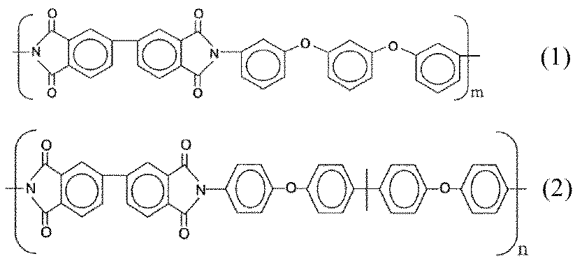
合成例で得られたブロック共重合ポリイミド溶液をNMPで更に希釈し、固形分10%のブロック共重合ポリイミド溶液とした。このブロック共重合ポリイミド溶液にビス(4-マレイミドフェニル)メタン(BMI-H、ケイ・アイ化成)を固形分重量比率35、ブロック共重合ポリイミドの固形分重量比率65として(即ち、樹脂溶液に含まれるビス(4-マレイミドフェニル)メタン固形分重量:樹脂溶液に含まれるブロック共重合ポリイミド固形分重量=35:65)60℃、20分間溶解混合して樹脂溶液とした。その後、離型層形成面に前記樹脂溶液を塗工し、窒素雰囲気下で、120℃で3分間、160℃で3分間乾燥処理後、最後に300℃で2分間加熱処理を行い、樹脂層を備える銅箔を作製した。なお、樹脂層の厚みは2μmとした。
(7)各種評価
・三次元算術平均高さ(Sa)の測定
金属箔表面の三次元算術平均粗さSaは、オリンパス株式会社製のレーザー顕微鏡LEXT OLS4100を用いてISO25178準拠モードによって測定した。なお、Saは任意の10か所で測定したSaの値の平均値をSaの値とした。Saの測定面積は縦258μm×横258μmとした。なお、測定時の温度は23~25℃とした。
・三次元算術平均高さ(Sa)の測定
金属箔表面の三次元算術平均粗さSaは、オリンパス株式会社製のレーザー顕微鏡LEXT OLS4100を用いてISO25178準拠モードによって測定した。なお、Saは任意の10か所で測定したSaの値の平均値をSaの値とした。Saの測定面積は縦258μm×横258μmとした。なお、測定時の温度は23~25℃とした。
・積層体の製造
各金属箔の離型層側表面に以下の樹脂基材1~3のいずれかを貼り合わせた。
基材1:三菱ガス化学(株)製 GHPL-830 MBT
基材2:日立化成工業(株)製 679-FG
基材3:住友ベークライト(株)製 EI-6785TS-F
積層プレスの温度、圧力、時間は、各基材メーカーの推奨条件を用いた。
各金属箔の離型層側表面に以下の樹脂基材1~3のいずれかを貼り合わせた。
基材1:三菱ガス化学(株)製 GHPL-830 MBT
基材2:日立化成工業(株)製 679-FG
基材3:住友ベークライト(株)製 EI-6785TS-F
積層プレスの温度、圧力、時間は、各基材メーカーの推奨条件を用いた。
・金属箔の剥離性の評価
積層体に対し、IPC-TM-650に準拠し、引張り試験機オートグラフ100で銅箔から樹脂基材を剥離する際の常態ピール強度を測定し、以下の基準で金属箔の剥離性を評価した。
B:2~200gf/cmの範囲であった。
C:200gf/cm超であった。
積層体に対し、IPC-TM-650に準拠し、引張り試験機オートグラフ100で銅箔から樹脂基材を剥離する際の常態ピール強度を測定し、以下の基準で金属箔の剥離性を評価した。
B:2~200gf/cmの範囲であった。
C:200gf/cm超であった。
・樹脂の剥離モードの評価
上記剥離後の樹脂基材の剥離面を電子顕微鏡で観察し、樹脂の剥離モード(凝集、界面、凝集と界面との混在)について観察した。樹脂の剥離モードについて、「界面」は、樹銅箔と樹脂との界面で剥離したことを示し、「凝集」は、剥離強度が強すぎて樹脂が破壊していることを示し、「混在」は、上記「界面」と「凝集」とが混在していることを示す。
上記の積層体の製造、剥離性の評価、樹脂の剥離モードの評価は、一度剥離した銅箔を再び樹脂基材と積層することで繰り返し2~4回行い、1回目~4回目までの各回で行った。
上記剥離後の樹脂基材の剥離面を電子顕微鏡で観察し、樹脂の剥離モード(凝集、界面、凝集と界面との混在)について観察した。樹脂の剥離モードについて、「界面」は、樹銅箔と樹脂との界面で剥離したことを示し、「凝集」は、剥離強度が強すぎて樹脂が破壊していることを示し、「混在」は、上記「界面」と「凝集」とが混在していることを示す。
上記の積層体の製造、剥離性の評価、樹脂の剥離モードの評価は、一度剥離した銅箔を再び樹脂基材と積層することで繰り返し2~4回行い、1回目~4回目までの各回で行った。

(評価結果)
実施例1~13は、いずれも樹脂基材と貼り合わせた後に物理的に剥離する工程を複数回繰り返して行うことができた。また、金属箔を樹脂基材から物理的に剥離する際の剥離性が良好であった。
比較例1は、樹脂基材と貼り合わせた後に物理的に剥離する工程を複数回繰り返して行うことができなかった。また、金属箔を樹脂基材から物理的に剥離する際の剥離性が不良であった。
実施例1~13は、いずれも樹脂基材と貼り合わせた後に物理的に剥離する工程を複数回繰り返して行うことができた。また、金属箔を樹脂基材から物理的に剥離する際の剥離性が良好であった。
比較例1は、樹脂基材と貼り合わせた後に物理的に剥離する工程を複数回繰り返して行うことができなかった。また、金属箔を樹脂基材から物理的に剥離する際の剥離性が不良であった。
Claims (26)
- 樹脂基材と貼り合わせた後に物理的に剥離する工程を複数回繰り返して行うことができる金属箔。
- 樹脂基材と貼り合わせた後に物理的に剥離する工程を2~4回繰り返して行うことができる請求項1に記載の金属箔。
- 三次元算術平均粗さSaが0.10~1.50μmである表面を有する請求項1又は2に記載の金属箔。
- 厚みが5~105μmである請求項1~3のいずれか一項に記載の金属箔。
- 前記金属箔が銅箔である請求項1~4のいずれか一項に記載の金属箔。
- 前記金属箔の表面に、粗化処理層、耐熱層、防錆層、クロメート処理層及びシランカップリング処理層からなる群から選択された一種以上の層を設けた請求項1~5のいずれか一項に記載の金属箔。
- 前記粗化処理層、耐熱層、防錆層、クロメート処理層及びシランカップリング処理層からなる群から選択された一種以上の層の表面に、樹脂層を設けた請求項6に記載の金属箔。
- 前記樹脂層が、接着用樹脂、プライマー又は半硬化状態の樹脂である請求項7に記載の金属箔。
- 請求項1~8のいずれか一項に記載の金属箔と、
前記金属箔の表面凹凸を有する面側に設けられた離型層であって、且つ、前記離型層側から前記金属箔へ樹脂基材を貼り合わせたときの前記樹脂基材を剥離可能にする離型層と、
を備えた離型層付き金属箔。 - 前記離型層が、次式:

に示すアルミネート化合物、チタネート化合物、ジルコネート化合物、これらの加水分解生成物、該加水分解生成物の縮合体を単独で又は複数組み合わせて用いてなる請求項9に記載の離型層付き金属箔。 - 前記離型層が、次式:
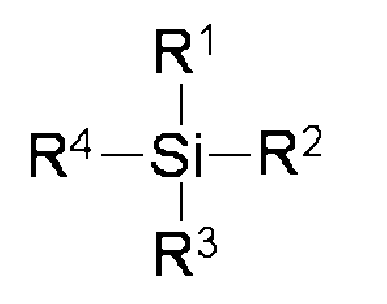
に示すシラン化合物、その加水分解生成物、該加水分解生成物の縮合体を単独で又は複数組み合わせて用いてなる請求項9に記載の離型層付き金属箔。 - 前記離型層が、分子内に2つ以下のメルカプト基を有する化合物を用いてなる請求項9に記載の離型層付き金属箔。
- 前記離型層表面に、樹脂層を設けた請求項9~12のいずれか一項に記載の離型層付き金属箔。
- 前記樹脂層が、接着用樹脂、プライマー又は半硬化状態の樹脂である請求項13に記載の離型層付き金属箔。
- 請求項1~8のいずれか一項に記載の金属箔、又は、請求項9~14のいずれか一項に記載の離型層付き金属箔と、前記金属箔又は前記離型層付き金属箔に設けられた樹脂基材とを備えた積層体。
- 前記樹脂基材が、プリプレグである、又は、熱硬化性樹脂を含む請求項15に記載の積層体。
- 請求項1~8のいずれか一項に記載の金属箔、又は、請求項9~14のいずれか一項に記載の離型層付き金属箔を備えたプリント配線板。
- 請求項17に記載のプリント配線板を備えた半導体パッケージ。
- 請求項17に記載のプリント配線板又は請求項16に記載の半導体パッケージを備えた電子機器。
- 請求項1~8のいずれか一項に記載の金属箔、又は、請求項9~14のいずれか一項に記載の離型層付き金属箔に、樹脂基材を貼り合わせる工程と、
前記樹脂基材から、前記金属箔又は前記離型層付き金属箔をエッチングすることなく引き剥がすことで、剥離面に前記金属箔又は前記離型層付き金属箔の表面プロファイルが転写された樹脂基材を得る工程と、
前記表面プロファイルが転写された樹脂基材の前記剥離面側に回路を形成する工程と、
を備えたプリント配線板の製造方法。 - 前記樹脂基材から引き剥がした金属箔を用いて、別の樹脂基材に表面プロファイルを転写することで、前記別の樹脂基材の前記剥離面側に回路を形成する工程をさらに1つ又は2つ以上備えた請求項20に記載のプリント配線板の製造方法。
- 前記表面プロファイルが転写された樹脂基材の前記剥離面側に形成する回路が、メッキパターン又は印刷パターンである請求項20又は21に記載のプリント配線板の製造方法。
- 請求項1~8のいずれか一項に記載の金属箔、又は、請求項9~14のいずれか一項に記載の離型層付き金属箔に、樹脂基材を貼り合わせる工程と、
前記樹脂基材から、前記金属箔又は前記離型層付き金属箔をエッチングすることなく引き剥がすことで、剥離面に前記金属箔又は前記離型層付き金属箔の表面プロファイルが転写された樹脂基材を得る工程と、
前記表面プロファイルが転写された樹脂基材の前記剥離面側にビルドアップ層を設ける工程と、
を備えたプリント配線板の製造方法。 - 前記樹脂基材から引き剥がした金属箔を用いて、別の樹脂基材に表面プロファイルを転写することで、前記別の樹脂基材の前記剥離面側にビルドアップ層を設ける工程をさらに1つ又は2つ以上備えた請求項23に記載のプリント配線板の製造方法。
- 前記ビルドアップ層を構成する樹脂が、液晶ポリマーまたはポリテトラフルオロエチレンを含む請求項23又は24に記載のプリント配線板の製造方法。
- 前記金属箔は、金属箔と樹脂基材とを貼り合わせた後に樹脂基材から金属箔を物理的に剥離する工程に1回以上使用された金属箔である請求項20~25のいずれか一項に記載のプリント配線板の製造方法。
Applications Claiming Priority (2)
| Application Number | Priority Date | Filing Date | Title |
|---|---|---|---|
| JP2015187538A JP6588290B2 (ja) | 2015-09-25 | 2015-09-25 | 離型層付き金属箔、積層体、プリント配線板、半導体パッケージ、電子機器、積層体の製造方法及びプリント配線板の製造方法 |
| JP2015-187538 | 2015-09-25 |
Publications (1)
| Publication Number | Publication Date |
|---|---|
| WO2017051908A1 true WO2017051908A1 (ja) | 2017-03-30 |
Family
ID=58386728
Family Applications (1)
| Application Number | Title | Priority Date | Filing Date |
|---|---|---|---|
| PCT/JP2016/078120 Ceased WO2017051908A1 (ja) | 2015-09-25 | 2016-09-23 | 金属箔、離型層付き金属箔、積層体、プリント配線板、半導体パッケージ、電子機器及びプリント配線板の製造方法 |
Country Status (3)
| Country | Link |
|---|---|
| JP (1) | JP6588290B2 (ja) |
| TW (1) | TWI645959B (ja) |
| WO (1) | WO2017051908A1 (ja) |
Families Citing this family (2)
| Publication number | Priority date | Publication date | Assignee | Title |
|---|---|---|---|---|
| JP7763483B2 (ja) * | 2022-03-28 | 2025-11-04 | ナミックス株式会社 | プリント配線板の製造方法 |
| JP7763484B2 (ja) * | 2022-03-28 | 2025-11-04 | ナミックス株式会社 | プリント配線板の製造方法 |
Citations (8)
| Publication number | Priority date | Publication date | Assignee | Title |
|---|---|---|---|---|
| JP2006093625A (ja) * | 2004-09-27 | 2006-04-06 | Matsushita Electric Works Ltd | 金属体付き絶縁体、アディティブメッキ用絶縁体、アディティブメッキ金属皮膜付き基板 |
| JP2014049645A (ja) * | 2012-08-31 | 2014-03-17 | Panasonic Corp | 剥離可能銅箔付き基板及び回路基板の製造方法 |
| WO2014054811A1 (ja) * | 2012-10-04 | 2014-04-10 | Jx日鉱日石金属株式会社 | 多層プリント配線基板の製造方法及びベース基材 |
| WO2015030256A1 (ja) * | 2013-09-02 | 2015-03-05 | Jx日鉱日石金属株式会社 | キャリア付銅箔、銅張積層板、プリント配線板、電子機器、及びプリント配線板の製造方法 |
| JP2015090980A (ja) * | 2013-11-04 | 2015-05-11 | サムソン エレクトロ−メカニックス カンパニーリミテッド. | 複合金属フィルムおよびこれを用いるプリント回路基板の回路パターン形成方法 |
| JP2015106629A (ja) * | 2013-11-29 | 2015-06-08 | 日本化薬株式会社 | 高周波回路用プリント配線基板 |
| JP2015109351A (ja) * | 2013-12-04 | 2015-06-11 | Jx日鉱日石金属株式会社 | 多層プリント配線基板の製造方法及びベース基材 |
| JP2015183240A (ja) * | 2014-03-25 | 2015-10-22 | Jx日鉱日石金属株式会社 | 表面処理銅箔、銅張積層板、プリント配線板、電子機器、半導体パッケージ用回路形成基板、半導体パッケージ及びプリント配線板の製造方法 |
-
2015
- 2015-09-25 JP JP2015187538A patent/JP6588290B2/ja active Active
-
2016
- 2016-09-23 WO PCT/JP2016/078120 patent/WO2017051908A1/ja not_active Ceased
- 2016-09-23 TW TW105130809A patent/TWI645959B/zh active
Patent Citations (8)
| Publication number | Priority date | Publication date | Assignee | Title |
|---|---|---|---|---|
| JP2006093625A (ja) * | 2004-09-27 | 2006-04-06 | Matsushita Electric Works Ltd | 金属体付き絶縁体、アディティブメッキ用絶縁体、アディティブメッキ金属皮膜付き基板 |
| JP2014049645A (ja) * | 2012-08-31 | 2014-03-17 | Panasonic Corp | 剥離可能銅箔付き基板及び回路基板の製造方法 |
| WO2014054811A1 (ja) * | 2012-10-04 | 2014-04-10 | Jx日鉱日石金属株式会社 | 多層プリント配線基板の製造方法及びベース基材 |
| WO2015030256A1 (ja) * | 2013-09-02 | 2015-03-05 | Jx日鉱日石金属株式会社 | キャリア付銅箔、銅張積層板、プリント配線板、電子機器、及びプリント配線板の製造方法 |
| JP2015090980A (ja) * | 2013-11-04 | 2015-05-11 | サムソン エレクトロ−メカニックス カンパニーリミテッド. | 複合金属フィルムおよびこれを用いるプリント回路基板の回路パターン形成方法 |
| JP2015106629A (ja) * | 2013-11-29 | 2015-06-08 | 日本化薬株式会社 | 高周波回路用プリント配線基板 |
| JP2015109351A (ja) * | 2013-12-04 | 2015-06-11 | Jx日鉱日石金属株式会社 | 多層プリント配線基板の製造方法及びベース基材 |
| JP2015183240A (ja) * | 2014-03-25 | 2015-10-22 | Jx日鉱日石金属株式会社 | 表面処理銅箔、銅張積層板、プリント配線板、電子機器、半導体パッケージ用回路形成基板、半導体パッケージ及びプリント配線板の製造方法 |
Also Published As
| Publication number | Publication date |
|---|---|
| JP2017063114A (ja) | 2017-03-30 |
| TWI645959B (zh) | 2019-01-01 |
| JP6588290B2 (ja) | 2019-10-09 |
| TW201718256A (zh) | 2017-06-01 |
Similar Documents
| Publication | Publication Date | Title |
|---|---|---|
| JP6204430B2 (ja) | 金属箔、離型層付き金属箔、積層体、プリント配線板、半導体パッケージ、電子機器及びプリント配線板の製造方法 | |
| JP5826322B2 (ja) | 表面処理銅箔、銅張積層板、プリント配線板、電子機器、半導体パッケージ用回路形成基板、半導体パッケージ及びプリント配線板の製造方法 | |
| JP6605271B2 (ja) | 離型層付き電解銅箔、積層体、半導体パッケージの製造方法、電子機器の製造方法及びプリント配線板の製造方法 | |
| JP6438370B2 (ja) | プリント配線板の製造方法、表面処理銅箔、積層体、プリント配線板、半導体パッケージ及び電子機器 | |
| TW201811557A (zh) | 附脫模層的銅箔、積層體、印刷配線板的製造方法及電子機器的製造方法 | |
| TWI660658B (zh) | 附脫模層金屬箔、金屬箔、積層體、印刷配線板、半導體封裝、電子機器及印刷配線板的製造方法 | |
| JP2018121085A (ja) | プリント配線板の製造方法 | |
| JP6498091B2 (ja) | 表面処理金属箔、積層体、プリント配線板、半導体パッケージ、電子機器 | |
| JP6588290B2 (ja) | 離型層付き金属箔、積層体、プリント配線板、半導体パッケージ、電子機器、積層体の製造方法及びプリント配線板の製造方法 | |
| WO2017051897A1 (ja) | 金属箔、離型層付き金属箔、積層体、プリント配線板、半導体パッケージ、電子機器及びプリント配線板の製造方法 | |
| JP6031624B2 (ja) | 表面処理銅箔、銅張積層板、プリント配線板の製造方法、半導体パッケージの製造方法及び電子機器の製造方法 | |
| JP5897755B2 (ja) | 表面処理銅箔、銅張積層板、プリント配線板、電子機器、半導体パッケージ、プリント配線板の製造方法、電子機器の製造方法、半導体パッケージの製造方法、樹脂基材の製造方法、銅箔の表面プロファイルを樹脂基材に転写する方法 | |
| JP2018171902A (ja) | 離型層付銅箔、積層体、プリント配線板の製造方法及び電子機器の製造方法 | |
| WO2017022807A1 (ja) | プリント配線板の製造方法、表面処理銅箔、積層体、プリント配線板、半導体パッケージ及び電子機器 |
Legal Events
| Date | Code | Title | Description |
|---|---|---|---|
| 121 | Ep: the epo has been informed by wipo that ep was designated in this application |
Ref document number: 16848696 Country of ref document: EP Kind code of ref document: A1 |
|
| NENP | Non-entry into the national phase |
Ref country code: DE |
|
| 122 | Ep: pct application non-entry in european phase |
Ref document number: 16848696 Country of ref document: EP Kind code of ref document: A1 |