WO2017051496A1 - 配線基板の製造方法、配線基板及び配線基板製造装置 - Google Patents
配線基板の製造方法、配線基板及び配線基板製造装置 Download PDFInfo
- Publication number
- WO2017051496A1 WO2017051496A1 PCT/JP2016/003767 JP2016003767W WO2017051496A1 WO 2017051496 A1 WO2017051496 A1 WO 2017051496A1 JP 2016003767 W JP2016003767 W JP 2016003767W WO 2017051496 A1 WO2017051496 A1 WO 2017051496A1
- Authority
- WO
- WIPO (PCT)
- Prior art keywords
- wiring board
- insulating layer
- layer
- seed layer
- treatment
- Prior art date
- Legal status (The legal status is an assumption and is not a legal conclusion. Google has not performed a legal analysis and makes no representation as to the accuracy of the status listed.)
- Ceased
Links
Images



Classifications
-
- H—ELECTRICITY
- H05—ELECTRIC TECHNIQUES NOT OTHERWISE PROVIDED FOR
- H05K—PRINTED CIRCUITS; CASINGS OR CONSTRUCTIONAL DETAILS OF ELECTRIC APPARATUS; MANUFACTURE OF ASSEMBLAGES OF ELECTRICAL COMPONENTS
- H05K3/00—Apparatus or processes for manufacturing printed circuits
- H05K3/10—Apparatus or processes for manufacturing printed circuits in which conductive material is applied to the insulating support in such a manner as to form the desired conductive pattern
- H05K3/18—Apparatus or processes for manufacturing printed circuits in which conductive material is applied to the insulating support in such a manner as to form the desired conductive pattern using precipitation techniques to apply the conductive material
-
- H—ELECTRICITY
- H05—ELECTRIC TECHNIQUES NOT OTHERWISE PROVIDED FOR
- H05K—PRINTED CIRCUITS; CASINGS OR CONSTRUCTIONAL DETAILS OF ELECTRIC APPARATUS; MANUFACTURE OF ASSEMBLAGES OF ELECTRICAL COMPONENTS
- H05K3/00—Apparatus or processes for manufacturing printed circuits
- H05K3/38—Improvement of the adhesion between the insulating substrate and the metal
-
- H—ELECTRICITY
- H05—ELECTRIC TECHNIQUES NOT OTHERWISE PROVIDED FOR
- H05K—PRINTED CIRCUITS; CASINGS OR CONSTRUCTIONAL DETAILS OF ELECTRIC APPARATUS; MANUFACTURE OF ASSEMBLAGES OF ELECTRICAL COMPONENTS
- H05K3/00—Apparatus or processes for manufacturing printed circuits
- H05K3/40—Forming printed elements for providing electric connections to or between printed circuits
- H05K3/42—Plated through-holes or plated via connections
Definitions
- the present invention relates to a method of manufacturing a wiring board in which an insulating layer and a conductive layer are stacked, a wiring board manufactured by the manufacturing method, and a wiring board manufacturing apparatus.
- a multilayer wiring board in which an insulating layer and a conductive layer (wiring layer) are alternately stacked is known.
- a part of the insulating layer or the conductive layer is removed by performing drilling or laser processing on the wiring board material in which the insulating layer is laminated on the conductive layer. , Form via holes and through holes.
- a smear is generated in the wiring substrate material due to the material forming the insulating layer or the conductive layer. Therefore, a desmear process is performed on the wiring board material to remove smear.
- Patent Document 1 discloses a substrate manufacturing method having a step of removing smear generated in a via formation step by wet desmear processing, and a step of forming a seed layer by electroless plating.
- the surface of the insulating layer is appropriately roughened in order to ensure the adhesion between the seed layer and the insulating layer. It is necessary to firmly fix the seed layer to the surface of the insulating layer by the anchor effect.
- the surface of the insulating layer is roughened by performing a wet desmearing process as the desmearing process.
- one mode of a manufacturing method of a wiring board concerning the present invention forms a penetration hole which penetrates the insulating layer to wiring board material by which an insulating layer was laminated on a conductive layer.
- the desmear treatment with ultraviolet light is performed, the surface roughening of the insulating layer can be suppressed. Therefore, the fine wiring pattern can be appropriately formed. Further, since the seed layer is formed by causing the material particles to collide and adhere to each other, the adhesion strength to the insulating layer can be secured by the seed layer regardless of the conventional anchor effect. In particular, a color center (structural defect or bonding defect) can be generated on the surface of the insulating layer by irradiation with ultraviolet light having a wavelength of 220 nm or less which does not pass through the insulating layer.
- material particles (electrically conductive material) are driven into the insulating layer, and energy is applied to the bonding defects present on the resin surface irradiated with ultraviolet light, whereby a new chemical bonding action can be made between the metal particles and the resin.
- a seed layer having a strong adhesion is formed as compared to the case where metal particles collide and adhere to a resin which has not been irradiated with ultraviolet light having a wavelength of 220 nm or less.
- the inventors have found that the adhesion between the insulating layer and the seed layer may be lowered depending on the time elapsed after the desmear treatment and the environment. Therefore, in the third step, the adhesion between the seed layer and the insulating layer is always ensured by forming the seed layer after surface modification treatment.
- the surface modification treatment may be performed by low pressure Ar plasma treatment, or ultraviolet light having a wavelength of 220 nm or less is irradiated in an atmosphere containing no oxygen.
- the surface modification treatment may be performed, the surface modification treatment may be performed using a chemical solution, or the surface modification treatment may be performed using a sodium hydroxide aqueous solution.
- the wiring board according to the present invention is manufactured by any of the above-described method for manufacturing a wiring board. Therefore, the wiring substrate can be a highly reliable fine wiring substrate in which the adhesion between the seed layer and the insulating layer is always ensured.
- an ultraviolet ray having a wavelength of 220 nm or less is applied to a wiring substrate material in which an insulating layer is stacked on a conductive layer and a through hole penetrating the insulating layer is formed.
- a seed layer forming portion for forming a seed layer by colliding and depositing material particles on the layer To remove the oxide film formed on the conductive material at the bottom of the through hole which has been subjected to the desmearing process for the wiring substrate material and the desmeared inside of the through hole and the insulating material.
- a seed layer forming portion for forming a seed layer by colliding and depositing material particles on the layer is possible to manufacture a highly reliable wiring board in which the adhesion between the seed layer and the insulating layer
- the present invention it is possible to realize miniaturization of the wiring pattern while always securing the adhesion between the seed layer and the insulating layer, and to manufacture a highly reliable micro wiring substrate.
- the objects, aspects and effects of the present invention described above as well as the objects, aspects and effects of the present invention not described above can be carried out by those skilled in the art by referring to the attached drawings and claims. It can be understood from the form (detailed description of the invention).
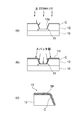
- FIG. 1 is a view showing a method of manufacturing a wiring board of the present embodiment.
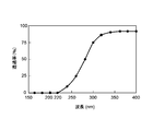
- FIG. 2 is a graph showing the ultraviolet light transmission characteristics of the epoxy resin.
- FIG. 3 is a diagram in which a resin that has received ultraviolet light of 220 nm or less is sputtered.
- FIG. 4 is a diagram in which a resin that has received 250 nm ultraviolet light is sputtered.
- FIG. 5 is a schematic view showing the configuration of a wiring board manufacturing apparatus.
- FIG. 1 is a view showing a method of manufacturing a wiring board of the present embodiment.
- the wiring substrate to be manufactured is a multilayer wiring substrate formed by laminating a conductive layer (wiring layer) and an insulating layer on a core substrate.
- the core substrate is made of, for example, a glass epoxy resin.
- a material which comprises a conductive layer (wiring layer) copper, nickel, gold etc. can be used, for example.
- the insulating layer is made of, for example, a resin containing a particulate filler made of an inorganic substance.
- an epoxy resin bismaleimide triazine resin, polyimide resin, polyester resin etc.
- a material which comprises a granular filler a silica, an alumina, mica
- a wiring board material in which the conductive layer 11 and the insulating layer 12 are laminated is formed.
- a method of forming the insulating layer 12 on the conductive layer 11 a method of curing the insulating layer forming material after applying the insulating layer forming material in which the particulate filler is contained in the liquid thermosetting resin
- the insulating layer 12 is processed by using a laser L or the like to form a via hole 12a having a depth reaching the conductive layer 11.
- a method of laser processing a method using a CO 2 laser, a method using a UV laser, or the like can be used.
- the method of forming the via holes 12a is not limited to laser processing, and for example, drilling may be used.
- the via hole 12a When the via hole 12a is formed in this manner, the inner wall surface (side wall) of the via hole 12a in the insulating layer 12, the peripheral region of the via hole 12a in the surface of the insulating layer 12, and the bottom of the via hole 12a, that is, the via hole 12a in the conductive layer 11 Smear (residue) S resulting from the material which comprises the conductive layer 11 and the insulating layer 12 arises in the exposed part etc.
- a process (desmear process) for removing the smear S is performed.
- the desmearing process a so-called photodesmearing process in which the smear S is removed by irradiating ultraviolet rays (UV) to the portion to be treated is used. More specifically, in the photodesmear process, an ultraviolet irradiation process step of irradiating the above-mentioned ultraviolet rays to the treated portion of the wiring board material and physical vibration are applied to the wiring board material after the ultraviolet irradiation process step. And physical vibration treatment process.
- UV ultraviolet rays
- the ultraviolet irradiation treatment can be performed, for example, in an atmosphere containing oxygen such as the air.
- an ultraviolet light source various lamps that emit ultraviolet light (vacuum ultraviolet light) having a wavelength of 220 nm or less, preferably 190 nm or less can be used.
- the reason for setting the wavelength to 220 nm is that when the wavelength of ultraviolet light exceeds 220 nm, it becomes difficult to decompose and remove the smear caused by the organic substance such as resin.
- the smear due to the organic substance is decomposed by the energy of the ultraviolet light and the ozone and active oxygen generated along with the irradiation of the ultraviolet light by irradiating the ultraviolet light having a wavelength of 220 nm or less in the ultraviolet irradiation treatment process.
- smears caused by inorganic substances, specifically, silica and alumina become brittle when irradiated with ultraviolet light.
- the ultraviolet light source for example, a xenon excimer lamp (peak wavelength 172 nm), low pressure mercury lamp (185 nm bright line) or the like in which xenon gas is sealed can be used. Among them, for example, a xenon excimer lamp is preferable as the one used for the desmear treatment.
- the processing region where the wiring substrate material to be processed is exposed to the ultraviolet light in the atmosphere of the processing gas containing oxygen is, for example, 120 ° C. or more and 190 ° C. or less (e.g. It is heated to ° C.
- the separation distance between the ultraviolet light emission window and the wiring substrate material to be processed is set to, for example, 0.3 mm.
- the illuminance of the ultraviolet light, the irradiation time of the ultraviolet light, and the like can be appropriately set in consideration of the residual state of the smear S and the like.
- the frequency of ultrasonic waves in the ultrasonic vibration processing is preferably, for example, 20 kHz or more and 70 kHz or less. When the frequency of the ultrasonic wave exceeds 70 kHz, it is difficult to break the smear caused by the inorganic substance and to separate it from the wiring board material.
- a liquid such as water and a gas such as air can be used as a vibration medium of ultrasonic waves.
- ultrasonic vibration processing can be performed by immersing the wiring substrate material, for example, in water and subjecting the water to ultrasonic vibration in this state. .
- the processing time of ultrasonic vibration processing is, for example, 10 seconds to 600 seconds.
- ultrasonic vibration processing can be performed by blowing compressed air onto the wiring substrate material while ultrasonically vibrating it.
- the pressure of the compressed air is preferably, for example, 0.2 MPa or more.
- the processing time of ultrasonic vibration processing with compressed air is, for example, 5 seconds to 60 seconds.
- the ultraviolet irradiation treatment step and the physical vibration treatment step may be performed once in this order, but it is preferable to alternately repeat the ultraviolet irradiation treatment step and the physical vibration treatment step.
- the number of repetitions of the ultraviolet irradiation processing step and the physical vibration processing step is appropriately set in consideration of the irradiation time of the ultraviolet light in each ultraviolet irradiation processing step, and is, for example, 1 to 5 times.
- ozone and active oxygen are generated by irradiating the processing gas containing oxygen with ultraviolet light having a wavelength of 220 nm or less in the ultraviolet irradiation treatment, and the smear S caused by the organic substance is decomposed by ozone and active oxygen to form a gas Be As a result, most of the smear S due to the organic substance is removed. At this time, the smear S due to the inorganic substance is exposed by the removal of the smear S due to the organic substance, and further becomes brittle due to the irradiation of the ultraviolet light.
- the remaining portion of the smear S due to the exposed inorganic substance and the smear S due to the organic substance is broken and removed by the mechanical action by the vibration.
- the difference in thermal expansion generated when each smear S is irradiated with ultraviolet light a slight gap is generated between the smears, and the smear S caused by the inorganic substance is It releases from wiring board material by giving physical vibration processing. As a result, the smear S due to the inorganic substance and the smear S due to the organic substance are completely removed from the wiring board material.
- the photodesmear process in the present embodiment since the ultraviolet irradiation process and the physical vibration process may be performed on the wiring substrate material, it is not necessary to use a chemical which requires the waste liquid process.
- a seed layer forming process for forming a seed layer is performed.
- the seed layer forming process as shown in FIG. 1D, a modification process of modifying the surface of the insulating layer 12 including the inner surface of the via hole 12a, and as shown in FIG. 1E, the insulating layer And forming the seed layer 13 on the upper surface of the via 12 and the inner surface of the via hole 12a.
- low pressure Ar plasma treatment is used as a surface reforming method in the reforming step.
- the target material T is disposed to face the wiring substrate material in an argon atmosphere, and the target material T is relative between the wiring substrate material and the target material T.
- a positive voltage is applied, and a voltage of a polarity at which the wiring board material becomes relatively negative is applied.
- argon plasma P is generated between the wiring substrate material and the target material T, and argon ions AI in the plasma P fly toward the wiring substrate material which is relatively at a negative potential, and thus insulation is achieved. It collides with the surface of layer 12. Due to this collision, the surface of the insulating layer 12 is reformed including the inner surface of the via hole 12a.
- sputtering is used as a method of forming the seed layer 13 in the forming step.
- a voltage having a voltage polarity reverse to the voltage polarity in the removing step is applied between the wiring substrate material and the target material T.
- argon plasma P is generated between the wiring substrate material and the target material T, and argon ions AI in the plasma P collide with the target material T which has a relatively negative potential.
- the target particles TP are knocked out of the target material T, and the target particles TP collide and adhere to the surface of the wiring substrate material.
- the seed layer 13 is formed.
- the target material T is used as the target material T to form a base layer (about 10 nm to 100 nm), and then the target material A seed layer (about 100 nm to 1000 nm) is formed using Cu (copper) as T.
- a resist pattern R is formed on the seed layer 13.
- a method of forming the resist pattern R for example, a method of forming a pattern by exposure and development after applying a resist on the seed layer 13 can be used.
- the plating layer 14 is formed from the inside of the via hole 12a to the opening of the resist pattern R by electrolytic plating using the seed layer 13 as a plating feed path.
- a layer (about 20 ⁇ m to 50 ⁇ m) made of Cu (copper) or the like can be used as the plating layer 14.
- the resist pattern R is removed, and then, as shown in FIG. 1 (i), the seed layer 13 is removed (flash etching) using the plating layer 14 as a mask.
- the step shown in FIG. 1 (b) corresponds to the first step of forming a through hole in the insulating layer stacked on the conductive layer, as shown in FIG. 1 (c).
- the step shown corresponds to a second step of performing desmear treatment by irradiating ultraviolet rays having a wavelength of 220 nm or less after the first step.
- the steps shown in FIGS. 1D and 1E correspond to the third step of forming a seed layer in the through hole and on the insulating layer after the second step.
- the step shown in) corresponds to the fourth step of forming a plating layer made of a conductive material by electrolytic plating on the seed layer.
- the seed layer 13 is formed by the sputtering method.
- the adhesion between the insulating layer and the seed layer has been secured by the anchor effect. That is, in order to secure the adhesion between the insulating layer and the seed layer, it has been considered preferable to roughen the surface of the insulating layer.
- the present inventor performs the desmearing process and the seed layer forming process which are a part of the manufacturing process of the wiring substrate by combining the photodesmear process and the sputtering method, without roughening the surface of the insulating layer. It has been found that the adhesion between the insulating layer and the seed layer can be secured.
- the photodesmear treatment can remove smear without roughening the surface of the object to be treated. Further, in the photodesmear treatment in the present embodiment, physical vibration treatment is performed subsequent to the ultraviolet irradiation treatment, so that it is possible to appropriately remove the smear caused by the organic substance and the smear caused by the inorganic substance. Furthermore, since the seed layer 13 is formed by sputtering, the seed layer 13 can be formed with sufficient adhesion strength on the insulating layer 12 whose surface is not roughened.
- the dense and strong seed layer 13 is formed on the insulating layer 12 Can.
- this point will be described in detail.
- FIG. 2 is a view showing the ultraviolet light transmission characteristic of the epoxy resin (25 ⁇ m film).
- the horizontal axis is the wavelength (nm) of ultraviolet light
- the vertical axis is the transmittance (%) of ultraviolet light.
- light passes through the resin in a region of wavelengths of 220 nm or more, that is, in a portion of visible light and near ultraviolet light, and the transmittance thereof becomes smaller as the wavelength becomes shorter.
- the transmittance thereof becomes smaller as the wavelength becomes shorter.
- the transmittance thereof becomes smaller as the wavelength becomes shorter.
- the ultraviolet light is almost transmitted through the resin.
- the ultraviolet light is slightly absorbed by the resin, but the absorption is so small that the ultraviolet light is not completely blocked. This is to absorb ultraviolet light in the entire thickness direction of the resin, and the resin excited by the ultraviolet light is widely distributed throughout the resin.
- FIG. 3 is a view showing a state in which a resin receiving ultraviolet light having a wavelength of 220 nm or less is sputtered, and FIG.
- FIGS. 3 and 4 are views showing a state in which a resin receiving ultraviolet light having a wavelength 250 nm is sputtered. It is.
- insulating layer 10 conductive layer 11 having a required pattern stacked on the surface of insulating layer 10, and insulating layer 12 stacked on insulating layer 10 including conductive layer 11.
- a part of the wiring board material configured to include
- UV ultraviolet light
- the ultraviolet light is the insulating layer 12 as described above. It is absorbed at the surface, and a color center (coupling defect, structural defect) C occurs on the surface of the insulating layer 12.
- the color center C is a defect which is excited by absorbing the above-mentioned ultraviolet light, and is generated by breaking a chemical bond between atoms or changing a bonding state.
- FIG. 3B when target particles (metal particles) TP flying from a sputtering source are bombarded onto the surface of the insulating layer 12 where the color center C is generated, the color center C will Firmly capture particles TP.
- a new chemical bonding action can be made between the metal particles and the resin by applying energy to the bonding defect present on the resin surface that has been irradiated with ultraviolet light.
- FIG. 3C is an enlarged view of the surface of the insulating layer 12 at this time.
- the adhesion between the insulating layer 12 that has been subjected to the ultraviolet light having a wavelength of 220 nm or less and the sputtered metal film (seed layer 13 in FIG. 1) becomes very strong.
- the distribution of the excited resin in the insulating layer 12 receiving the ultraviolet light are sparse and distributed throughout the insulating layer 12. That is, as shown in FIG. 4A, the color centers C are not distributed on the surface of the insulating layer 12 but are distributed inside the insulating layer 12. Therefore, as shown in FIG. 4B, even if target particles (metal particles) TP flying from a sputtering source are implanted into the surface of the insulating layer 12, the trapping effect of the metal particles TP is small. That is, as shown in FIG.
- the seed layer formation treatment using the sputtering method is performed after the ultraviolet irradiation treatment using the ultraviolet light having a wavelength of 220 nm or less in the ultraviolet irradiation treatment to form a dense and strong seed layer 13 on the insulating layer 12. Can be formed. Therefore, the plating layer 14 subjected to electrolytic plating based on the seed layer 13 exhibits high adhesion to the insulating layer 12. Thus, the adhesion between the insulating layer 12 and the seed layer 13 can be secured without roughening the surface of the insulating layer 12. As a result, a highly reliable fine wiring board can be realized.
- the surface of the insulating layer 12 can be kept smooth, high frequency response can be improved. At higher frequencies, the skin effect has the property that the signal is concentrated on the surface of the conductor. If the surface of the insulating layer 12 is roughened to obtain an anchor effect as in the above-described conventional case, the signal transmission distance also increases, and accordingly, the transmission loss increases and the responsiveness deteriorates. In the present embodiment, the transmission loss can be reduced, and the response can be improved. As described above, in the present embodiment, the adhesion between the insulating layer 12 and the seed layer 13 can be ensured, but the adhesion may be lowered depending on the standing time after the photodesmear treatment and the environmental conditions. The inventors found it. Therefore, in the present embodiment, by performing reduced-pressure Ar plasma treatment as preparation for forming the seed layer 13, it is possible to prevent the decrease in adhesion and stably form the seed layer 13 strongly connected to the insulating layer 12. .
- Reference Example 1 The wiring board material was subjected to wet desmear treatment using a permanganic acid solution, the protective film was peeled off, and then a 1 ⁇ m seed layer was formed by electroless copper plating. Furthermore, on the substrate, a Cu layer (plated layer) of 30 ⁇ m was formed by electrolytic plating.
- Reference Example 2 The wiring board material was subjected to wet desmear treatment using a permanganic acid solution, and then the oxide film was removed by wet etching using a mixed solution of hydrogen peroxide and sulfuric acid. Then, after the protective film was peeled off, a 1 ⁇ m seed layer was formed by electroless copper plating. Furthermore, on the substrate, a Cu layer (plated layer) of 30 ⁇ m was formed by electrolytic plating.
- Example 3 The wiring board material was subjected to photodesmear treatment using ultraviolet light of wavelength 172 nm, and then ion etching was performed for 1 minute to remove the oxide film.
- Example 5 The wiring board material was subjected to photodesmear treatment using ultraviolet light of wavelength 172 nm, and then ion etching was performed for 10 minutes to remove the oxide film.
- the Cu layer of the substrate is cut with a cutter knife to a width of 1 cm in accordance with the method described in JIS H8630 Annex 1, and then pulled. The peel test which peels off in the direction of 90 degrees with a tester was performed on each of five samples. And the average value and standard deviation of peel strength (kgf / cm) were calculated
- the average peel strength was 0.420 kgf / cm, and the standard deviation was ⁇ 0.085 kgf / cm.
- the average peel strength was 0.422 kgf / cm and the standard deviation was ⁇ 0.035 kgf / cm.
- the average value of the peel strength was 0.450 kgf / cm, and the standard deviation was ⁇ 0.020 kgf / cm.
- the average value of the peel strength is less than 0.5 kgf / cm.
- Comparative Example 1 in which the photodesmear treatment was performed, the average value of peel strength was 0.620 kgf / cm, and it was confirmed that the peel strength was improved by performing the photodesmear treatment.
- the standard deviation of the peel strength was a large value of ⁇ 0.100 kgf / cm. This is considered to be because the color center was inactivated in part of the sample because no surface modification treatment was performed after the photodesmear treatment.
- the average value of the peel strength was 0.610 kgf / cm, and the standard deviation was ⁇ 0.030 kgf / cm.
- Example 2 the average value of the peel strength was 0.650 kgf / cm, and the standard deviation was ⁇ 0.030 kgf / cm. It is considered that the surface modification treatment was performed after the photodesmear treatment even for a short time of 0.5 minutes, so that the non-activated color center was reactivated and the standard deviation decreased as compared with Comparative Example 1. Moreover, the average value of the peel strength is further improved as compared with Comparative Example 1 by using the low pressure Ar plasma treatment as the photodesmear treatment. In Example 3, the average peel strength was 0.700 kgf / cm, and the standard deviation was ⁇ 0.030 kgf / cm. In Example 4, the average peel strength was 0.848 kgf / cm, and the standard deviation was ⁇ 0.025 kgf / cm.
- Example 5 the average peel strength was 0.832 kgf / cm, and the standard deviation was ⁇ 0.015 kgf / cm.
- Example 6 the average peel strength was 0.838 kgf / cm, and the standard deviation was ⁇ 0.015 kgf / cm. It was found that when the surface modification treatment time was 10 minutes or more, the average peel strength reached a plateau but the standard deviation further decreased.
- FIG. 5 is a schematic view showing the configuration of a wiring board manufacturing apparatus.
- FIG. 5A shows a configuration of a wiring substrate manufacturing apparatus 210 for manufacturing a wiring substrate without using the above-described protective film
- FIG. 5B shows a wiring substrate using the above-described protective film.
- the configuration of the wiring board manufacturing apparatus 220 to be manufactured is shown.
- the wiring substrate manufacturing apparatus 210 shown in FIG. 5A includes an ultraviolet irradiation device 211, an ultrasonic cleaning / drying device 212, and a plasma / sputtering device 213.
- the ultraviolet irradiation device 211 performs an ultraviolet irradiation process in the photodesmear process on the work (wiring substrate material).
- the ultrasonic cleaning / drying apparatus 212 performs an ultrasonic vibration process (ultrasonic cleaning process) as a physical vibration process in the photodesmear process, and then performs a drying process to dry the workpiece.
- the plasma sputtering apparatus 213 adopts a low pressure Ar plasma method and a sputtering method, and performs a process of modifying the work surface after the photodesmear process to form a seed layer.
- the wiring substrate manufacturing apparatus 220 shown in FIG. 5B includes an ultraviolet irradiation device 221, an ultrasonic cleaning / drying device 222, a mask peeler 223, and a plasma / sputtering device 224.
- the ultraviolet irradiation device 221 and the ultrasonic cleaning / drying device 222 are the same as the ultraviolet irradiation device 211 and the ultrasonic cleaning / drying device 212.
- the mask peeler apparatus 223 performs a process of removing the protective film from the work after the photodesmear process.
- the plasma sputtering apparatus 224 adopts a low pressure Ar plasma method and a sputtering method, and performs a process of modifying the surface of the work after removing the protective film to form a seed layer.
- UV irradiation devices 211 and 221 correspond to UV irradiation units
- ultrasonic cleaning / drying devices 212 and 222 correspond to vibration application units
- plasma sputtering devices 213 and 224 are seed layer forming units. It corresponds.
- the seed layer may be formed by ion plating.
- the same effect as in the case where the seed layer is formed by sputtering can be obtained. That is, in the case of a method of forming a seed layer by causing material particles (metal particles) to collide and adhere as in a sputtering method or an ion plating method, the same effect as the above embodiment can be obtained.
- surface modification may be performed by immersing the substrate material in a chemical solution.
- medical solution the sodium hydroxide aqueous solution is preferable, for example.
- the surface may be reformed by irradiating ultraviolet rays having a wavelength of 220 nm or less in an atmosphere not containing oxygen such as in a vacuum or in a nitrogen atmosphere at atmospheric pressure.
- ultraviolet rays having a wavelength of 220 nm or less in an atmosphere not containing oxygen such as in a vacuum or in a nitrogen atmosphere at atmospheric pressure.
- the present invention is also applicable to a descum device and a surface reforming device.
- the descum apparatus is, for example, an apparatus for removing residues such as solder resist (Photo Solder Resist: PSR), dry film (DFR) and the like used in the manufacturing process.
- the surface modification device is, for example, a device that performs adhesion improvement and wettability improvement by cleaning before and after plating, roughening of the material surface, and the like.
- the light processing apparatus of the present invention is applicable to, for example, a light ashing processing apparatus, a resist removal processing apparatus, a dry cleaning processing apparatus, and the like.
- SYMBOLS 10 Insulating layer, 11 ... Conducting layer, 12 ... Insulating layer, 12a ... Via hole, 13 ... Seed layer, 14 ... Plating layer, C ... Color center, L ... Laser, R ... Resist pattern, S ... Smear, TP ... Target particle
Landscapes
- Engineering & Computer Science (AREA)
- Manufacturing & Machinery (AREA)
- Microelectronics & Electronic Packaging (AREA)
- Manufacturing Of Printed Wiring (AREA)
- Printing Elements For Providing Electric Connections Between Printed Circuits (AREA)
Abstract
シード層と絶縁層との密着性を担保しつつ、配線パターンの微細化を実現する配線基板の製造方法が開示される。この方法は、配線基板の製造工程として、導電層の上に絶縁層が積層された配線基板材料に対して、絶縁層を貫通する貫通孔を形成する第一工程と、第一工程の後、配線基板材料に対して波長220nm以下の紫外線を照射することにより、当該配線基板材料のデスミア処理を行う第二工程と、第二工程の後、配線基板材料に対して表面改質処理を施し、貫通孔内および絶縁層の上に、材料粒子を衝突させ付着させることでシード層を形成する第三工程と、シード層の上に、電解めっきにより導電材料からなるめっき層を形成する第四工程と、を含む。
Description
本発明は、絶縁層と導電層とが積層されてなる配線基板の製造方法、その製造方法によって製造された配線基板、及び配線基板製造装置に関する。
半導体集積回路素子等の半導体素子を搭載するための配線基板としては、絶縁層と導電層(配線層)とが交互に積層されてなる多層配線基板が知られている。
多層配線基板の製造工程の一例としては、先ず、絶縁層が導電層の上に積層されてなる配線基板材料に、ドリル加工やレーザ加工を施すことによって絶縁層や導電層の一部を除去し、ビアホールやスルーホールを形成する。このとき、配線基板材料には絶縁層や導電層を構成する材料に起因するスミア(残渣)が生じる。そのため、当該配線基板材料に対してスミアを除去するデスミア処理を行う。
多層配線基板の製造工程の一例としては、先ず、絶縁層が導電層の上に積層されてなる配線基板材料に、ドリル加工やレーザ加工を施すことによって絶縁層や導電層の一部を除去し、ビアホールやスルーホールを形成する。このとき、配線基板材料には絶縁層や導電層を構成する材料に起因するスミア(残渣)が生じる。そのため、当該配線基板材料に対してスミアを除去するデスミア処理を行う。
次いで、絶縁層の上やビアホール等の内面にシード層を形成し、絶縁層の上にレジストパターンを形成した後、電解めっきによって導電材料を積層する。その後、レジストパターンとシード層とを除去することで導体回路パターンを形成する。その後も種々の工程を経て、半導体素子は作製される。
特許文献1には、湿式デスミア処理によってビア形成工程で生じたスミアを除去する工程と、無電解めっきによってシード層を形成する工程と、を有する基板製造方法が開示されている。
特許文献1には、湿式デスミア処理によってビア形成工程で生じたスミアを除去する工程と、無電解めっきによってシード層を形成する工程と、を有する基板製造方法が開示されている。
上記特許文献1に記載の技術では、デスミア処理後、無電解めっきによりシード層を形成するが、シード層と絶縁層との密着性を確保するためには、絶縁層の表面を適度に粗い状態とし、アンカー効果によりシード層を絶縁層表面に強固に固定する必要がある。上記特許文献1に記載の技術では、デスミア処理として湿式デスミア処理を行うことにより、絶縁層表面を粗化している。
ところで、近年、半導体素子は小型化傾向にあり、配線基板も微細化が求められている。しかしながら、上記のようにアンカー効果を得るために絶縁層の表面を粗くすると、その上に形成する配線パターン、特に、L/S(ライン/スペース)=10/10μm以下の微細配線パターンが立たなくなり、配線基板を微細化することができない。
そこで、本発明は、シード層と絶縁層との密着性を担保しつつ、配線パターンの微細化を実現することができる配線基板の製造方法、配線基板及び配線基板製造装置を提供することを課題としている。
ところで、近年、半導体素子は小型化傾向にあり、配線基板も微細化が求められている。しかしながら、上記のようにアンカー効果を得るために絶縁層の表面を粗くすると、その上に形成する配線パターン、特に、L/S(ライン/スペース)=10/10μm以下の微細配線パターンが立たなくなり、配線基板を微細化することができない。
そこで、本発明は、シード層と絶縁層との密着性を担保しつつ、配線パターンの微細化を実現することができる配線基板の製造方法、配線基板及び配線基板製造装置を提供することを課題としている。
上記課題を解決するために、本発明に係る配線基板の製造方法の一態様は、導電層の上に絶縁層が積層された配線基板材料に対して、前記絶縁層を貫通する貫通孔を形成する第一工程と、前記貫通孔が形成された前記配線基板材料に対して、波長220nm以下の紫外線を照射することにより、当該配線基板材料のデスミア処理を行う第二工程と、前記デスミア処理された前記配線基板材料に対して表面改質処理を施し、前記貫通孔内および前記絶縁層の上に、材料粒子を衝突させ付着させることでシード層を形成する第三工程と、前記シード層の上に、電解めっきにより導電材料からなるめっき層を形成する第四工程と、を含む。
このように、紫外線によるデスミア処理を行うので、絶縁層表面の粗化を抑制することができる。そのため、微細配線パターンを適切に形成することができる。また、材料粒子を衝突させ付着させることでシード層を形成するので、従来のようなアンカー効果によらずに、シード層によって絶縁層との密着強度を担保することができる。特に、絶縁層を透過しない波長220nm以下の紫外線を照射することで、絶縁層表面にカラーセンター(構造欠陥、結合欠陥)を生じさせることができる。このとき、材料粒子(導電材料)が絶縁層に打ち込まれ、紫外線照射を受けた樹脂表面に存在する結合欠陥部にエネルギーが加わることで金属粒子と樹脂間にあらたな化学的結合作用ができる。これにより、波長220nm以下の紫外線の照射を受けていない樹脂に金属粒子が衝突し付着するのと比較して、強い密着力をもつシード層ができる。
このような絶縁層とシード層との密着性について、デスミア処理後の経過時間や環境によっては密着性が低下する場合があることを発明者らは見いだした。そこで、第三工程では、表面改質処理を施した上でシード層を形成することでシード層と絶縁層との密着性を常に担保している。
上記の配線基板の製造方法において、前記第三工程は、減圧Arプラズマ処理により前記表面改質処理を行ってもよいし、波長220nm以下の紫外線を、酸素を含まない雰囲気中で照射することにより前記表面改質処理を行ってもよいし、薬液により前記表面改質処理を行ってもよいし、水酸化ナトリウム水溶液により前記表面改質処理を行ってもよい。これにより、絶縁層との密着性が常に確保されたシード層を形成することができる。
上記の配線基板の製造方法において、前記第三工程は、減圧Arプラズマ処理により前記表面改質処理を行ってもよいし、波長220nm以下の紫外線を、酸素を含まない雰囲気中で照射することにより前記表面改質処理を行ってもよいし、薬液により前記表面改質処理を行ってもよいし、水酸化ナトリウム水溶液により前記表面改質処理を行ってもよい。これにより、絶縁層との密着性が常に確保されたシード層を形成することができる。
さらに、本発明に係る配線基板は、上記のいずれかの配線基板の製造方法により製造される。したがって、当該配線基板は、シード層と絶縁層との密着性が常に担保された信頼性の高い微細配線基板とすることができる。
また、本発明に係る配線基板製造装置の一態様は、導電層の上に絶縁層が積層され、前記絶縁層を貫通する貫通孔が形成された配線基板材料に対して、波長220nm以下の紫外線を照射することにより、当該配線基板材料のデスミア処理を行う紫外線照射部と、前記デスミア処理された前記貫通孔の底の導電材料に形成された酸化膜を除去し、前記貫通孔内および前記絶縁層の上に、材料粒子を衝突させ付着させることでシード層を形成するシード層形成部と、を備える。これにより、シード層と絶縁層との密着性が常に担保された信頼性の高い配線基板を製造することができる。
また、本発明に係る配線基板製造装置の一態様は、導電層の上に絶縁層が積層され、前記絶縁層を貫通する貫通孔が形成された配線基板材料に対して、波長220nm以下の紫外線を照射することにより、当該配線基板材料のデスミア処理を行う紫外線照射部と、前記デスミア処理された前記貫通孔の底の導電材料に形成された酸化膜を除去し、前記貫通孔内および前記絶縁層の上に、材料粒子を衝突させ付着させることでシード層を形成するシード層形成部と、を備える。これにより、シード層と絶縁層との密着性が常に担保された信頼性の高い配線基板を製造することができる。
本発明によれば、シード層と絶縁層との密着性を常に担保しつつ、配線パターンの微細化を実現することができ、信頼性の高い微細配線基板を製造することができる。
上記した本発明の目的、態様及び効果並びに上記されなかった本発明の目的、態様及び効果は、当業者であれば添付図面及び請求の範囲の記載を参照することにより下記の発明を実施するための形態(発明の詳細な説明)から理解できるであろう。
上記した本発明の目的、態様及び効果並びに上記されなかった本発明の目的、態様及び効果は、当業者であれば添付図面及び請求の範囲の記載を参照することにより下記の発明を実施するための形態(発明の詳細な説明)から理解できるであろう。
以下、本発明の実施の形態を図面に基づいて説明する。
図1は、本実施形態の配線基板の製造方法を示す図である。本実施形態において、製造対象の配線基板は、コア基板上に導電層(配線層)と絶縁層とを積層してなる多層配線基板である。コア基板は、例えばガラスエポキシ樹脂などによって構成されている。導電層(配線層)を構成する材料としては、例えば、銅、ニッケル、金などを用いることができる。
絶縁層は、例えば無機物質よりなる粒状フィラーが含有された樹脂などによって構成されている。このような樹脂としては、例えば、エポキシ樹脂、ビスマレイミドトリアジン樹脂、ポリイミド樹脂、ポリエステル樹脂などを用いることができる。また、粒状フィラーを構成する材料としては、例えば、シリカ、アルミナ、マイカ、珪酸塩、硫酸バリウム、水酸化マグネシウム、酸化チタンなどを用いることができる。
図1は、本実施形態の配線基板の製造方法を示す図である。本実施形態において、製造対象の配線基板は、コア基板上に導電層(配線層)と絶縁層とを積層してなる多層配線基板である。コア基板は、例えばガラスエポキシ樹脂などによって構成されている。導電層(配線層)を構成する材料としては、例えば、銅、ニッケル、金などを用いることができる。
絶縁層は、例えば無機物質よりなる粒状フィラーが含有された樹脂などによって構成されている。このような樹脂としては、例えば、エポキシ樹脂、ビスマレイミドトリアジン樹脂、ポリイミド樹脂、ポリエステル樹脂などを用いることができる。また、粒状フィラーを構成する材料としては、例えば、シリカ、アルミナ、マイカ、珪酸塩、硫酸バリウム、水酸化マグネシウム、酸化チタンなどを用いることができる。
多層配線基板を製造する場合、先ず、図1(a)に示すように、導電層11と絶縁層12とが積層されてなる配線基板材料を形成する。導電層11の上に絶縁層12を形成する方法としては、液状の熱硬化性樹脂中に粒状フィラーが含有されてなる絶縁層形成材料を塗布した後、当該絶縁層形成材料を硬化処理する方法や、粒状フィラーが含有された絶縁シートを熱圧着等によって貼り合わせる方法などを利用することができる。
次に、図1(b)に示すように、絶縁層12を、レーザLを用いて加工するなどにより、導電層11に到達する深さのビアホール12aを形成する。レーザ加工の方法としては、CO2レーザを用いる方法や、UVレーザを用いる方法などを利用することができる。なお、ビアホール12aを形成する方法は、レーザ加工に限定されるものではなく、例えばドリル加工などを用いてもよい。
このようにしてビアホール12aを形成すると、絶縁層12におけるビアホール12aの内壁面(サイドウォール)、絶縁層12の表面におけるビアホール12aの周辺領域、およびビアホール12aの底部、即ち導電層11におけるビアホール12aによって露出した部分などには、導電層11や絶縁層12を構成する材料に起因するスミア(残渣)Sが生じる。
このようにしてビアホール12aを形成すると、絶縁層12におけるビアホール12aの内壁面(サイドウォール)、絶縁層12の表面におけるビアホール12aの周辺領域、およびビアホール12aの底部、即ち導電層11におけるビアホール12aによって露出した部分などには、導電層11や絶縁層12を構成する材料に起因するスミア(残渣)Sが生じる。
そこで、図1(c)に示すように、スミアSを除去する処理(デスミア処理)を行う。本実施形態では、デスミア処理として、被処理部分に対して紫外線(UV)を照射することでスミアSを除去する、所謂フォトデスミア処理を用いる。より具体的には、フォトデスミア処理では、配線基板材料の被処理部分に対して上記の紫外線を照射する紫外線照射処理工程と、この紫外線照射処理工程の後、配線基板材料に物理的振動を与える物理的振動処理工程とを行う。
ここで、フォトデスミア処理について詳細に説明する。
紫外線照射処理は、例えば大気などの酸素を含む雰囲気下において行うことができる。紫外線光源としては、波長220nm以下、好ましくは190nm以下の紫外線(真空紫外線)を出射する種々のランプを利用できる。ここで、波長220nmとしたのは、紫外線の波長が220nmを超える場合には、樹脂などの有機物質に起因するスミアを分解除去することが困難となるためである。
有機物質に起因するスミアは、紫外線照射処理工程において、波長220nm以下の紫外線を照射することにより、紫外線のエネルギーおよび紫外線の照射に伴って生ずるオゾンや活性酸素によって分解される。また、無機物質に起因するスミア、具体的にはシリカやアルミナは、紫外線が照射されることによって脆いものとなる。
紫外線照射処理は、例えば大気などの酸素を含む雰囲気下において行うことができる。紫外線光源としては、波長220nm以下、好ましくは190nm以下の紫外線(真空紫外線)を出射する種々のランプを利用できる。ここで、波長220nmとしたのは、紫外線の波長が220nmを超える場合には、樹脂などの有機物質に起因するスミアを分解除去することが困難となるためである。
有機物質に起因するスミアは、紫外線照射処理工程において、波長220nm以下の紫外線を照射することにより、紫外線のエネルギーおよび紫外線の照射に伴って生ずるオゾンや活性酸素によって分解される。また、無機物質に起因するスミア、具体的にはシリカやアルミナは、紫外線が照射されることによって脆いものとなる。
紫外線光源としては、例えば、キセノンガスを封入したキセノンエキシマランプ(ピーク波長172nm)、低圧水銀ランプ(185nm輝線)などを用いることができる。なかでも、デスミア処理に用いるものとしては、例えばキセノンエキシマランプが好適である。
上記の紫外線照射処理を行う紫外線照射装置において、被処理対象である配線基板材料が酸素を含む処理気体の雰囲気中で紫外線に曝される処理領域は、例えば120℃以上190℃以下(例えば、150℃)に加熱される。また、紫外線出射窓と被処理対象である配線基板材料との離間距離は、例えば0.3mmに設定される。なお、紫外線の照度や紫外線の照射時間などは、スミアSの残留状態などを考慮して適宜設定することができる。
上記の紫外線照射処理を行う紫外線照射装置において、被処理対象である配線基板材料が酸素を含む処理気体の雰囲気中で紫外線に曝される処理領域は、例えば120℃以上190℃以下(例えば、150℃)に加熱される。また、紫外線出射窓と被処理対象である配線基板材料との離間距離は、例えば0.3mmに設定される。なお、紫外線の照度や紫外線の照射時間などは、スミアSの残留状態などを考慮して適宜設定することができる。
また、物理的振動処理は、例えば超音波振動処理によって行うことができる。超音波振動処理における超音波の周波数は、例えば20kHz以上70kHz以下であることが好ましい。超音波の周波数が70kHzを超えると、無機物質に起因するスミアを破壊して配線基板材料から離脱させることが困難となるためである。
このような超音波振動処理においては、超音波の振動媒体として、水などの液体および空気などの気体を用いることができる。
具体的に説明すると、振動媒体として水を用いる場合には、配線基板材料を、例えば水中に浸漬し、この状態で、当該水を超音波振動させることにより、超音波振動処理を行うことができる。超音波の振動媒体として液体を用いる場合には、超音波振動処理の処理時間は、例えば10秒間~600秒間である。
このような超音波振動処理においては、超音波の振動媒体として、水などの液体および空気などの気体を用いることができる。
具体的に説明すると、振動媒体として水を用いる場合には、配線基板材料を、例えば水中に浸漬し、この状態で、当該水を超音波振動させることにより、超音波振動処理を行うことができる。超音波の振動媒体として液体を用いる場合には、超音波振動処理の処理時間は、例えば10秒間~600秒間である。
また、振動媒体として空気を用いる場合には、圧縮空気を超音波振動させながら配線基板材料に吹きつけることにより、超音波振動処理を行うことができる。ここで、圧縮空気の圧力は、例えば0.2MPa以上であることが好ましい。また、圧縮空気による超音波振動処理の処理時間は、例えば5秒間~60秒間である。
上記の紫外線照射処理工程および物理的振動処理工程は、この順でそれぞれ1回ずつ行ってもよいが、紫外線照射処理工程および物理的振動処理工程を交互に繰り返して行うことが好ましい。ここで、紫外線照射処理工程および物理的振動処理工程の繰り返し回数は、各紫外線照射処理工程における紫外線の照射時間などを考慮して適宜設定されるが、例えば1回~5回である。
上記の紫外線照射処理工程および物理的振動処理工程は、この順でそれぞれ1回ずつ行ってもよいが、紫外線照射処理工程および物理的振動処理工程を交互に繰り返して行うことが好ましい。ここで、紫外線照射処理工程および物理的振動処理工程の繰り返し回数は、各紫外線照射処理工程における紫外線の照射時間などを考慮して適宜設定されるが、例えば1回~5回である。
このように、紫外線照射処理において波長220nm以下の紫外線を、酸素を含む処理気体に照射することによりオゾンや活性酸素が生じ、有機物質に起因するスミアSは、オゾンや活性酸素によって分解されてガス化される。その結果、有機物質に起因するスミアSは、その大部分が除去される。このとき、無機物質に起因するスミアSは、有機物質に起因するスミアSの除去により露出し、さらに、紫外線が照射されることによって脆いものとなる。
そして、その状態で物理的振動処理を施すことにより、露出した無機物質に起因するスミアSや有機物質に起因するスミアSの残部は、振動による機械的作用によって破壊され、除去される。或いは、無機物質に起因するスミアSの収縮や、各スミアSに紫外線を照射したときに発生する熱膨張の差などによって、スミア間にわずかな隙間が生じ、無機物質に起因するスミアSは、物理的振動処理を施すことにより配線基板材料から離脱する。その結果、配線基板材料から無機物質に起因するスミアSと、有機物質に起因するスミアSとが完全に除去される。
本実施形態におけるフォトデスミア処理によれば、配線基板材料に対して紫外線照射処理および物理的振動処理を行えばよいので、廃液処理が必要となる薬品を用いることが不要である。
フォトデスミア処理が完了すると、次に、シード層を形成するシード層形成処理を行う。このシード層形成処理では、図1(d)に示すように、ビアホール12aの内面を含んだ絶縁層12の表面を改質する改質工程と、図1(e)に示すように、絶縁層12の上面およびビアホール12aの内面にシード層13を形成する形成工程とを行う。
フォトデスミア処理が完了すると、次に、シード層を形成するシード層形成処理を行う。このシード層形成処理では、図1(d)に示すように、ビアホール12aの内面を含んだ絶縁層12の表面を改質する改質工程と、図1(e)に示すように、絶縁層12の上面およびビアホール12aの内面にシード層13を形成する形成工程とを行う。
本実施形態では、改質工程における表面改質方法として減圧Arプラズマ処理を用いる。具体的には、図1(d)に示すように、アルゴン雰囲気中で配線基板材料に対向してターゲット材料Tを配置し、配線基板材料とターゲット材料Tとの間に、ターゲット材料Tが相対的に正電位となり配線基板材料が相対的に負電位となる極性の電圧を印加する。これにより、配線基板材料とターゲット材料Tとの間では、アルゴンのプラズマPが発生し、プラズマP中のアルゴンイオンAIが、相対的に負電位になっている配線基板材料に向かって飛び、絶縁層12の表面に衝突する。この衝突によってビアホール12aの内面も含めて絶縁層12の表面が改質される。
本実施形態では、形成工程におけるシード層13の形成方法としてスパッタリングを用いる。具体的には、図1(e)に示すように、除去工程における電圧極性とは逆向きの電圧極性を有する電圧を、配線基板材料とターゲット材料Tとの間に印加する。これにより、配線基板材料とターゲット材料Tとの間では、アルゴンのプラズマPが発生し、プラズマP中のアルゴンイオンAIが、相対的に負電位になっているターゲット材料Tに衝突する。この衝突によってターゲット材料Tからターゲット粒子TPがたたき出され、そのターゲット粒子TPが配線基板材料の表面に衝突して付着する。このようにターゲット粒子TPを付着させることでシード層13を形成する。なお、シード層13を形成するスパッタリングでは、例えば、密着強度確保のために、先ずターゲット材料TとしてTi(チタン)を用いてベースとなる層(10nm~100nm程度)を形成し、その後、ターゲット材料TとしてCu(銅)を用いてシード層(100nm~1000nm程度)を形成する。
次に、図1(f)に示すように、シード層13の上にレジストパターンRを形成する。レジストパターンRの形成方法としては、例えば、シード層13の上にレジストを塗布した後、露光・現像によってパターンを形成する方法を用いることができる。
次に、図1(g)に示すように、シード層13をめっき給電経路に利用する電解めっきにより、ビアホール12a内からレジストパターンRの開口部にかけてめっき層14を形成する。めっき層14としては、例えば、Cu(銅)などからなる層(20μm~50μm程度)を用いることができる。
その後、図1(h)に示すように、レジストパターンRを除去し、次いで、図1(i)に示すように、めっき層14をマスクにしてシード層13を除去(フラッシュエッチング)する。
次に、図1(g)に示すように、シード層13をめっき給電経路に利用する電解めっきにより、ビアホール12a内からレジストパターンRの開口部にかけてめっき層14を形成する。めっき層14としては、例えば、Cu(銅)などからなる層(20μm~50μm程度)を用いることができる。
その後、図1(h)に示すように、レジストパターンRを除去し、次いで、図1(i)に示すように、めっき層14をマスクにしてシード層13を除去(フラッシュエッチング)する。
なお、図1に示す各工程のうち、図1(b)に示す工程が、導電層の上に積層された絶縁層に貫通孔を形成する第一工程に対応し、図1(c)に示す工程が、第一工程の後に、波長220nm以下の紫外線を照射してデスミア処理を行う第二工程に対応している。また、図1(d)および図1(e)に示す工程が、第二工程の後に、上記貫通孔内および絶縁層の上にシード層を形成する第三工程に対応し、図1(g)に示す工程が、シード層の上に電解めっきにより導電材料からなるめっき層を形成する第四工程に対応している。
このように、本実施形態では、フォトデスミア処理を用いてスミアSを除去した後、スパッタリング法によりシード層13を形成する。
従来、絶縁層とシード層との密着性は、アンカー効果により担保していた。すなわち、絶縁層とシード層との密着性を確保するためには、絶縁層の表面を粗化することが好ましいとされていた。しかしながら、絶縁層の表面を粗化すると、特にL/S(ライン/スペース)=10/10μm以下の微細配線パターンが立たなくなるため、微細配線基板の作製が困難となる。そのため、微細配線基板を作製するためには、絶縁層の表面を粗化することなく、絶縁層とシード層との密着性を担保する必要がある。本発明者は、配線基板の製造工程の一部であるデスミア処理とシード層形成処理とを、フォトデスミア処理とスパッタリング法との組み合わせにより行うことで、絶縁層の表面を粗化することなく、絶縁層とシード層との密着性を担保することができることを見出した。
従来、絶縁層とシード層との密着性は、アンカー効果により担保していた。すなわち、絶縁層とシード層との密着性を確保するためには、絶縁層の表面を粗化することが好ましいとされていた。しかしながら、絶縁層の表面を粗化すると、特にL/S(ライン/スペース)=10/10μm以下の微細配線パターンが立たなくなるため、微細配線基板の作製が困難となる。そのため、微細配線基板を作製するためには、絶縁層の表面を粗化することなく、絶縁層とシード層との密着性を担保する必要がある。本発明者は、配線基板の製造工程の一部であるデスミア処理とシード層形成処理とを、フォトデスミア処理とスパッタリング法との組み合わせにより行うことで、絶縁層の表面を粗化することなく、絶縁層とシード層との密着性を担保することができることを見出した。
フォトデスミア処理は、被処理物体の表面を粗くすることなく、スミアを除去することができる。また、本実施形態におけるフォトデスミア処理では、紫外線照射処理に続いて物理的振動処理を実施するので、有機物質に起因するスミアと無機物質に起因するスミアとを適切に除去することができる。
さらに、スパッタリング法を用いてシード層13を形成するので、表面が粗化されていない絶縁層12の上に、シード層13を十分な密着強度で形成することができる。特に、紫外線照射処理において波長220nm以下の紫外線を用い、当該紫外線照射処理の後にスパッタリング法を用いたシード層形成処理を実施するので、絶縁層12の上に緻密強固なシード層13を形成することができる。以下、この点について詳細に説明する。
さらに、スパッタリング法を用いてシード層13を形成するので、表面が粗化されていない絶縁層12の上に、シード層13を十分な密着強度で形成することができる。特に、紫外線照射処理において波長220nm以下の紫外線を用い、当該紫外線照射処理の後にスパッタリング法を用いたシード層形成処理を実施するので、絶縁層12の上に緻密強固なシード層13を形成することができる。以下、この点について詳細に説明する。
図2は、エポキシ樹脂(25μm膜)の紫外線透過率特性を示す図である。図2において、横軸は紫外線の波長(nm)、縦軸は紫外線の透過率(%)である。
この図2に示すように、波長220nm以上の領域、即ち可視光線および近紫外線の一部の領域では、光は樹脂を透過し、その透過率は波長が短くなるにしたがって小さくなる。具体的には、波長300nmを超える領域では、光は樹脂をほぼ透過する。波長300nm以下では、紫外線は樹脂にやや吸収されるが、その吸収は小さく紫外線が完全に遮られるほどではない。これは、樹脂の厚さ方向全体で紫外線を吸収するためであり、その紫外線により励起された樹脂は、樹脂の全体に広く分布する。
この図2に示すように、波長220nm以上の領域、即ち可視光線および近紫外線の一部の領域では、光は樹脂を透過し、その透過率は波長が短くなるにしたがって小さくなる。具体的には、波長300nmを超える領域では、光は樹脂をほぼ透過する。波長300nm以下では、紫外線は樹脂にやや吸収されるが、その吸収は小さく紫外線が完全に遮られるほどではない。これは、樹脂の厚さ方向全体で紫外線を吸収するためであり、その紫外線により励起された樹脂は、樹脂の全体に広く分布する。
一方、波長220nm以下の紫外線は、樹脂を透過しない。この吸光度は高く、紫外線は樹脂の表面層で吸収される。さらに短波長になると、樹脂の極表面で紫外線は完全に吸収され、紫外線の吸収により発生した励起箇所は樹脂表面に層状に分布する。
そして、このような活性な樹脂部は、スパッタリングによって飛来したターゲット粒子が樹脂に打ち込まれたときのエネルギーによって新たな結合を作り出し、強固にターゲット粒子を固定する。
図3は、波長220nm以下の紫外線を受けた樹脂にスパッタを施したときの状態を示す図であり、図4は、波長250nmの紫外線を受けた樹脂にスパッタを施したときの状態を示す図である。これら図3、図4では、絶縁層10と、絶縁層10の表面上に積層された所要のパターンを有する導電層11と、導電層11を含む絶縁層10上に積層された絶縁層12とを含んで構成される配線基板材料の一部を示している。
そして、このような活性な樹脂部は、スパッタリングによって飛来したターゲット粒子が樹脂に打ち込まれたときのエネルギーによって新たな結合を作り出し、強固にターゲット粒子を固定する。
図3は、波長220nm以下の紫外線を受けた樹脂にスパッタを施したときの状態を示す図であり、図4は、波長250nmの紫外線を受けた樹脂にスパッタを施したときの状態を示す図である。これら図3、図4では、絶縁層10と、絶縁層10の表面上に積層された所要のパターンを有する導電層11と、導電層11を含む絶縁層10上に積層された絶縁層12とを含んで構成される配線基板材料の一部を示している。
ビアホール12aに残留するスミア(不図示)を除去するフォトデスミア処理として、図3(a)に示すように、波長220nm以下の紫外線(UV)を照射した場合、上述したように紫外線は絶縁層12表面で吸収され、絶縁層12の表面にカラーセンター(結合欠陥、構造欠陥)Cが生じる。カラーセンターCとは、上記の紫外線を吸収することで励起され、原子同士の化学結合が切れたり結合状態が変化したりすることで生成される欠陥である。
このようにカラーセンターCが生じている絶縁層12表面に対し、図3(b)に示すように、スパッタ源から飛来するターゲット粒子(金属粒子)TPが打ち込まれると、カラーセンターCがその金属粒子TPを強固に捕獲する。つまり、紫外線照射を受けた樹脂表面に存在する結合欠陥部にエネルギーが加わることで、金属粒子と樹脂との間にあらたな化学的結合作用ができる。図3(c)は、このときの絶縁層12表面の拡大図である。このように、波長220nm以下の紫外線を受けた絶縁層12とスパッタを施した金属膜(図1のシード層13)との密着性は、非常に強固となる。
一方、図3に示す配線基板材料と同様の配線基板材料に対し、フォトデスミア処理として、例えば波長250nmの紫外線を照射した場合には、紫外線を受けた絶縁層12では、励起された樹脂の分布が疎で絶縁層12全体に分布する。すなわち、図4(a)に示すように、カラーセンターCは絶縁層12の表面に分布せず、絶縁層12の内部に分布する。
そのため、この絶縁層12表面に対し、図4(b)に示すように、スパッタ源から飛来するターゲット粒子(金属粒子)TPを打ち込んでも、金属粒子TPの捕獲作用は少ない。すなわち、図4(c)に、このときの絶縁層12表面の拡大図を示すように、絶縁層12表面と金属粒子TPとの特別な結合作用は無く、絶縁層12上に形成される金属膜(図1のシード層13)の密着力は強化されない。
そのため、この絶縁層12表面に対し、図4(b)に示すように、スパッタ源から飛来するターゲット粒子(金属粒子)TPを打ち込んでも、金属粒子TPの捕獲作用は少ない。すなわち、図4(c)に、このときの絶縁層12表面の拡大図を示すように、絶縁層12表面と金属粒子TPとの特別な結合作用は無く、絶縁層12上に形成される金属膜(図1のシード層13)の密着力は強化されない。
本実施形態では、紫外線照射処理において波長220nm以下の紫外線を用い、当該紫外線照射処理の後にスパッタリング法を用いたシード層形成処理を実施することで、絶縁層12の上に緻密強固なシード層13を形成することができる。したがって、このシード層13をベースに電解めっきを施しためっき層14は、絶縁層12に対して高い密着性を示す。このように、絶縁層12の表面を粗化することなく、絶縁層12とシード層13との密着性を担保することができる。その結果、信頼性の高い微細配線基板を実現することができる。
さらに、絶縁層12の表面を平滑に保つことができるので、高周波応答性を向上させることができる。周波数が高くなると、表皮効果により信号は導体の表面に集中するという性質を持つ。上記従来のように、アンカー効果を得るために絶縁層12の表面を粗くすると、信号の伝達距離も大きくなるため、それに伴って伝送損失が大きくなり、応答性が悪くなってしまう。本実施形態では、上記伝送損失を低減し、応答性を向上させることができる。
このように、本実施形態では、絶縁層12とシード層13との密着性を担保することができるが、フォトデスミア処理後の放置時間や環境条件によっては密着性が低下する場合があることを発明者らは見いだした。そこで、本実施形態では、シード層13形成の準備として減圧Arプラズマ処理を行うことで、密着性低下を回避し、絶縁層12に強固に接続したシード層13を安定して形成することができる。
このように、本実施形態では、絶縁層12とシード層13との密着性を担保することができるが、フォトデスミア処理後の放置時間や環境条件によっては密着性が低下する場合があることを発明者らは見いだした。そこで、本実施形態では、シード層13形成の準備として減圧Arプラズマ処理を行うことで、密着性低下を回避し、絶縁層12に強固に接続したシード層13を安定して形成することができる。
絶縁層12とシード層13との密着性低下の原因としては、波長220nm以下の紫外線を用いた紫外線照射処理において形成されたカラーセンターCの不活性化が推察される。減圧Arプラズマ処理を行うと表面改質によってカラーセンターCが活性化すると考えられ、改質された表面状態が保たれている間にシード層13を形成することにより、図3で説明したような結合作用が確実に得られると考えられる。
(実施例)
次に、本発明の効果を確認するために行った実施例について説明する。
<配線基板材料>
先ず、ガラスエポキシ樹脂と銅からなるプリプレグのコア材に、25μmのエポキシ樹脂を両面真空ラミネートし、高圧プレスとベーキングにより作成した積層体(エポキシ基板)を用意した。この積層体に厚さ38μmのPETフィルムによる保護膜を貼り、その後、ビア加工機(UVレーザ)によってレーザ加工を施すことにより、ブラインドビアを、500μmピッチで格子状に作成した。ビア開口径は、φ50μmとした。このようにして、配線基板材料を得た。また、このとき、配線基板材料のブラインドビアの底部に、スミアが残留していることを確認した。
次に、本発明の効果を確認するために行った実施例について説明する。
<配線基板材料>
先ず、ガラスエポキシ樹脂と銅からなるプリプレグのコア材に、25μmのエポキシ樹脂を両面真空ラミネートし、高圧プレスとベーキングにより作成した積層体(エポキシ基板)を用意した。この積層体に厚さ38μmのPETフィルムによる保護膜を貼り、その後、ビア加工機(UVレーザ)によってレーザ加工を施すことにより、ブラインドビアを、500μmピッチで格子状に作成した。ビア開口径は、φ50μmとした。このようにして、配線基板材料を得た。また、このとき、配線基板材料のブラインドビアの底部に、スミアが残留していることを確認した。
<参考例1>
上記配線基板材料に対し、過マンガン酸液を利用したウェットデスミア処理を施し、保護膜を剥がした後、無電解銅めっきにより1μmのシード層を形成した。さらに、その基板に、電解めっきにより30μmのCu層(めっき層)を形成した。
<参考例2>
上記配線基板材料に対し、過マンガン酸液を利用したウェットデスミア処理を施した後、過酸化水素と硫酸を混合した溶液を用いたウェットエッチングにより酸化膜除去を行った。そして、保護膜を剥がした後、無電解銅めっきにより1μmのシード層を形成した。さらに、その基板に、電解めっきにより30μmのCu層(めっき層)を形成した。
上記配線基板材料に対し、過マンガン酸液を利用したウェットデスミア処理を施し、保護膜を剥がした後、無電解銅めっきにより1μmのシード層を形成した。さらに、その基板に、電解めっきにより30μmのCu層(めっき層)を形成した。
<参考例2>
上記配線基板材料に対し、過マンガン酸液を利用したウェットデスミア処理を施した後、過酸化水素と硫酸を混合した溶液を用いたウェットエッチングにより酸化膜除去を行った。そして、保護膜を剥がした後、無電解銅めっきにより1μmのシード層を形成した。さらに、その基板に、電解めっきにより30μmのCu層(めっき層)を形成した。
<参考例3>
上記配線基板材料に対し、過マンガン酸液を利用したウェットデスミア処理を施した後、10分間のイオンエッチングを施して酸化膜除去を行った。そして、保護膜を剥がした後、スパッタリング法により0.33μm(Ti/Cu=0.03μm/0.3μm)のシード層を形成した。さらに、その基板に、電解めっきにより30μmのCu層(めっき層)を形成した。
<比較例1>
上記配線基板材料に対し、波長172nmの紫外線を用いたフォトデスミア処理を施し、保護膜を剥がした後、スパッタリング法により0.33μm(Ti/Cu=0.03μm/0.3μm)のシード層を形成した。さらに、その基板に、電解めっきにより30μmのCu層(めっき層)を形成した。なお、フォトデスミア処理においては、紫外線照射処理と物理的振動処理(超音波振動処理)とを実施した。
上記配線基板材料に対し、過マンガン酸液を利用したウェットデスミア処理を施した後、10分間のイオンエッチングを施して酸化膜除去を行った。そして、保護膜を剥がした後、スパッタリング法により0.33μm(Ti/Cu=0.03μm/0.3μm)のシード層を形成した。さらに、その基板に、電解めっきにより30μmのCu層(めっき層)を形成した。
<比較例1>
上記配線基板材料に対し、波長172nmの紫外線を用いたフォトデスミア処理を施し、保護膜を剥がした後、スパッタリング法により0.33μm(Ti/Cu=0.03μm/0.3μm)のシード層を形成した。さらに、その基板に、電解めっきにより30μmのCu層(めっき層)を形成した。なお、フォトデスミア処理においては、紫外線照射処理と物理的振動処理(超音波振動処理)とを実施した。
<実施例1>
上記配線基板材料に対し、波長172nmの紫外線を用いたフォトデスミア処理を施した後、過酸化水素と硫酸を混合した溶液を用いたウェットエッチングにより酸化膜除去を行った。そして、保護膜を剥がした後、スパッタリング法により0.33μm(Ti/Cu=0.03μm/0.3μm)のシード層を形成した。さらに、その基板に、電解めっきにより30μmのCu層(めっき層)を形成した。なお、以下全ての実施例で、フォトデスミア処理においては、紫外線照射処理と物理的振動処理(超音波振動処理)とを実施した。
上記配線基板材料に対し、波長172nmの紫外線を用いたフォトデスミア処理を施した後、過酸化水素と硫酸を混合した溶液を用いたウェットエッチングにより酸化膜除去を行った。そして、保護膜を剥がした後、スパッタリング法により0.33μm(Ti/Cu=0.03μm/0.3μm)のシード層を形成した。さらに、その基板に、電解めっきにより30μmのCu層(めっき層)を形成した。なお、以下全ての実施例で、フォトデスミア処理においては、紫外線照射処理と物理的振動処理(超音波振動処理)とを実施した。
<実施例2>
上記配線基板材料に対し、波長172nmの紫外線を用いたフォトデスミア処理を施した後、0.5分間のイオンエッチングを施して酸化膜除去を行った。そして、保護膜を剥がした後、スパッタリング法により0.33μm(Ti/Cu=0.03μm/0.3μm)のシード層を形成した。さらに、その基板に、電解めっきにより30μmのCu層(めっき層)を形成した。
<実施例3>
上記配線基板材料に対し、波長172nmの紫外線を用いたフォトデスミア処理を施した後、1分間のイオンエッチングを施して酸化膜除去を行った。そして、保護膜を剥がした後、スパッタリング法により0.33μm(Ti/Cu=0.03μm/0.3μm)のシード層を形成した。さらに、その基板に、電解めっきにより30μmのCu層(めっき層)を形成した。
上記配線基板材料に対し、波長172nmの紫外線を用いたフォトデスミア処理を施した後、0.5分間のイオンエッチングを施して酸化膜除去を行った。そして、保護膜を剥がした後、スパッタリング法により0.33μm(Ti/Cu=0.03μm/0.3μm)のシード層を形成した。さらに、その基板に、電解めっきにより30μmのCu層(めっき層)を形成した。
<実施例3>
上記配線基板材料に対し、波長172nmの紫外線を用いたフォトデスミア処理を施した後、1分間のイオンエッチングを施して酸化膜除去を行った。そして、保護膜を剥がした後、スパッタリング法により0.33μm(Ti/Cu=0.03μm/0.3μm)のシード層を形成した。さらに、その基板に、電解めっきにより30μmのCu層(めっき層)を形成した。
<実施例4>
上記配線基板材料に対し、波長172nmの紫外線を用いたフォトデスミア処理を施した後、5分間のイオンエッチングを施して酸化膜除去を行った。そして、保護膜を剥がした後、スパッタリング法により0.33μm(Ti/Cu=0.03μm/0.3μm)のシード層を形成した。さらに、その基板に、電解めっきにより30μmのCu層(めっき層)を形成した。
<実施例5>
上記配線基板材料に対し、波長172nmの紫外線を用いたフォトデスミア処理を施した後、10分間のイオンエッチングを施して酸化膜除去を行った。そして、保護膜を剥がした後、スパッタリング法により0.33μm(Ti/Cu=0.03μm/0.3μm)のシード層を形成した。さらに、その基板に、電解めっきにより30μmのCu層(めっき層)を形成した。
上記配線基板材料に対し、波長172nmの紫外線を用いたフォトデスミア処理を施した後、5分間のイオンエッチングを施して酸化膜除去を行った。そして、保護膜を剥がした後、スパッタリング法により0.33μm(Ti/Cu=0.03μm/0.3μm)のシード層を形成した。さらに、その基板に、電解めっきにより30μmのCu層(めっき層)を形成した。
<実施例5>
上記配線基板材料に対し、波長172nmの紫外線を用いたフォトデスミア処理を施した後、10分間のイオンエッチングを施して酸化膜除去を行った。そして、保護膜を剥がした後、スパッタリング法により0.33μm(Ti/Cu=0.03μm/0.3μm)のシード層を形成した。さらに、その基板に、電解めっきにより30μmのCu層(めっき層)を形成した。
<実施例6>
上記配線基板材料に対し、波長172nmの紫外線を用いたフォトデスミア処理を施した後、20分間のイオンエッチングを施して酸化膜除去を行った。そして、保護膜を剥がした後、スパッタリング法により0.33μm(Ti/Cu=0.03μm/0.3μm)のシード層を形成した。さらに、その基板に、電解めっきにより30μmのCu層(めっき層)を形成した。
上記の参考例1~3、比較例1、実施例1~6について、基板のCu層をJIS H8630付属書1に記載の方法に準拠して、1cmの幅にカッターナイフで切り込みを入れ、引っ張り試験器で90度方向に引き剥がすピール試験をそれぞれ5つの試料について行った。そして、ピール強度(kgf/cm)の平均値と標準偏差を求めた。その結果を表1に示す。
上記配線基板材料に対し、波長172nmの紫外線を用いたフォトデスミア処理を施した後、20分間のイオンエッチングを施して酸化膜除去を行った。そして、保護膜を剥がした後、スパッタリング法により0.33μm(Ti/Cu=0.03μm/0.3μm)のシード層を形成した。さらに、その基板に、電解めっきにより30μmのCu層(めっき層)を形成した。
上記の参考例1~3、比較例1、実施例1~6について、基板のCu層をJIS H8630付属書1に記載の方法に準拠して、1cmの幅にカッターナイフで切り込みを入れ、引っ張り試験器で90度方向に引き剥がすピール試験をそれぞれ5つの試料について行った。そして、ピール強度(kgf/cm)の平均値と標準偏差を求めた。その結果を表1に示す。

表1に示すように、参考例1では、ピール強度の平均値は0.420kgf/cmであり、標準偏差は±0.085kgf/cmであった。
また、参考例2では、ピール強度の平均値は0.422kgf/cmであり、標準偏差は±0.035kgf/cmであった。
また、参考例3では、ピール強度の平均値は0.450kgf/cmであり、標準偏差は±0.020kgf/cmであった。
このように、ウェットデスミア処理を施した参考例1~3は、いずれもピール強度の平均値が0.5kgf/cm未満となっている。
また、参考例2では、ピール強度の平均値は0.422kgf/cmであり、標準偏差は±0.035kgf/cmであった。
また、参考例3では、ピール強度の平均値は0.450kgf/cmであり、標準偏差は±0.020kgf/cmであった。
このように、ウェットデスミア処理を施した参考例1~3は、いずれもピール強度の平均値が0.5kgf/cm未満となっている。
これに対してフォトデスミア処理を施した比較例1では、ピール強度の平均値は0.620kgf/cmであり、フォトデスミア処理を施すことでピール強度が向上することが確かめられた。
但し、比較例1では、ピール強度の標準偏差は±0.100kgf/cmという大きい値であった。これは、フォトデスミア処理の後に表面改質処理を行っていないため、試料の一部でカラーセンターが非活性化したためと考えられる。
実施例1では、ピール強度の平均値は0.610kgf/cmであり、標準偏差は±0.030kgf/cmであった。フォトデスミア処理の後に表面改質処理を行ったため、非活性化したカラーセンターが再活性化されて、比較例1に較べて標準偏差が減少したと考えられる。但し、表面改質処理として薬液処理を用いたため、ピール強度の平均値は、少しではあるが比較例1よりも減少している。
但し、比較例1では、ピール強度の標準偏差は±0.100kgf/cmという大きい値であった。これは、フォトデスミア処理の後に表面改質処理を行っていないため、試料の一部でカラーセンターが非活性化したためと考えられる。
実施例1では、ピール強度の平均値は0.610kgf/cmであり、標準偏差は±0.030kgf/cmであった。フォトデスミア処理の後に表面改質処理を行ったため、非活性化したカラーセンターが再活性化されて、比較例1に較べて標準偏差が減少したと考えられる。但し、表面改質処理として薬液処理を用いたため、ピール強度の平均値は、少しではあるが比較例1よりも減少している。
実施例2では、ピール強度の平均値は0.650kgf/cmであり、標準偏差±0.030kgf/cmであった。0.5分という短時間でも、フォトデスミア処理の後に表面改質処理を行ったため、非活性化したカラーセンターが再活性化されて、比較例1に較べて標準偏差が減少したと考えられる。また、フォトデスミア処理として減圧Arプラズマ処理を用いたことで、ピール強度の平均値も比較例1に較べてさらに向上している。
実施例3では、ピール強度の平均値は0.700kgf/cmであり、標準偏差は±0.030kgf/cmであった。
実施例4では、ピール強度の平均値は0.848kgf/cmであり、標準偏差は±0.025kgf/cmであった。
実施例3では、ピール強度の平均値は0.700kgf/cmであり、標準偏差は±0.030kgf/cmであった。
実施例4では、ピール強度の平均値は0.848kgf/cmであり、標準偏差は±0.025kgf/cmであった。
表面改質処理の時間が延びるにつれてピール強度の平均値が向上し、標準偏差もさらに減少することが確かめられた。
実施例5では、ピール強度の平均値は0.832kgf/cmであり、標準偏差は±0.015kgf/cmであった。
実施例6では、ピール強度の平均値は0.838kgf/cmであり、標準偏差は±0.015kgf/cmであった。
表面改質処理の時間が10分以上になると、ピール強度の平均値は頭打ちになったが、標準偏差はさらに減少することが分かった。
実施例5では、ピール強度の平均値は0.832kgf/cmであり、標準偏差は±0.015kgf/cmであった。
実施例6では、ピール強度の平均値は0.838kgf/cmであり、標準偏差は±0.015kgf/cmであった。
表面改質処理の時間が10分以上になると、ピール強度の平均値は頭打ちになったが、標準偏差はさらに減少することが分かった。
以上説明したように、波長220nm以下の紫外線を用いたフォトデスミア処理と、スパッタリングによるシード層の形成処理との組み合わせにより、シード層と絶縁層表面との高い密着性を担保することができ、シード層の形成処理で絶縁層表面の改質処理を行うことで密着性のばらつきが抑制され、信頼性の高い基板を実現することができる。さらに、樹脂表面を平滑に保つことができるので、微細配線形成のためのレジストパターンを安定して形成することができ、微細配線基板を精度良く作製することができる。
(配線基板製造装置)
以上説明した配線基板の製造は、以下に示す配線基板製造装置により実現することができる。
図5は、配線基板製造装置の構成を示す概略図である。ここで、図5(a)は、上述した保護膜を用いずに配線基板を製造する配線基板製造装置210の構成を示し、図5(b)は、上述した保護膜を用いて配線基板を製造する配線基板製造装置220の構成を示している。
図5(a)に示す配線基板製造装置210は、紫外線照射装置211と、超音波洗浄・乾燥装置212と、プラズマ・スパッタ装置213と、を備える。紫外線照射装置211は、ワーク(配線基板材料)に対してフォトデスミア処理における紫外線照射処理を行う。超音波洗浄・乾燥装置212は、フォトデスミア処理における物理的振動処理として超音波振動処理(超音波洗浄処理)を行った後、ワークを乾燥する乾燥処理を行う。プラズマ・スパッタ装置213は、減圧Arプラズマ法とスパッタリング法を採用し、フォトデスミア処理後のワーク表面を改質してシード層を形成する処理を行う。
以上説明した配線基板の製造は、以下に示す配線基板製造装置により実現することができる。
図5は、配線基板製造装置の構成を示す概略図である。ここで、図5(a)は、上述した保護膜を用いずに配線基板を製造する配線基板製造装置210の構成を示し、図5(b)は、上述した保護膜を用いて配線基板を製造する配線基板製造装置220の構成を示している。
図5(a)に示す配線基板製造装置210は、紫外線照射装置211と、超音波洗浄・乾燥装置212と、プラズマ・スパッタ装置213と、を備える。紫外線照射装置211は、ワーク(配線基板材料)に対してフォトデスミア処理における紫外線照射処理を行う。超音波洗浄・乾燥装置212は、フォトデスミア処理における物理的振動処理として超音波振動処理(超音波洗浄処理)を行った後、ワークを乾燥する乾燥処理を行う。プラズマ・スパッタ装置213は、減圧Arプラズマ法とスパッタリング法を採用し、フォトデスミア処理後のワーク表面を改質してシード層を形成する処理を行う。
図5(b)に示す配線基板製造装置220は、紫外線照射装置221と、超音波洗浄・乾燥装置222と、マスクピーラー装置223と、プラズマ・スパッタ装置224と、を備える。紫外線照射装置221及び超音波洗浄・乾燥装置222は、紫外線照射装置211及び超音波洗浄・乾燥装置212と同様である。マスクピーラー装置223は、フォトデスミア処理後のワークから保護膜を除去する処理を行う。プラズマ・スパッタ装置224は、減圧Arプラズマ法とスパッタリング法を採用し、保護膜を除去した後のワーク表面を改質してシード層を形成する処理を行う。
このような配線基板製造装置210,220によれば、シード層と絶縁層との密着性が常に担保された信頼性の高い配線基板の製造を実現することができる。
なお、図5において、紫外線照射装置211及び221が紫外線照射部に対応し、超音波洗浄・乾燥装置212及び222が振動付与部に対応し、プラズマ・スパッタ装置213及び224がシード層形成部に対応している。
このような配線基板製造装置210,220によれば、シード層と絶縁層との密着性が常に担保された信頼性の高い配線基板の製造を実現することができる。
なお、図5において、紫外線照射装置211及び221が紫外線照射部に対応し、超音波洗浄・乾燥装置212及び222が振動付与部に対応し、プラズマ・スパッタ装置213及び224がシード層形成部に対応している。
(変形例)
上記実施形態においては、スパッタリング法によりシード層を形成する場合について説明したが、これに限定されるものではない。例えば、イオンプレーティング法によりシード層を形成してもよい。この場合にも、スパッタリング法によりシード層を形成した場合と同様の効果が得られる。すなわち、スパッタリング法やイオンプレーティング法のように、材料粒子(金属粒子)を衝突させ付着させることでシード層を形成する手法であれば、上記実施形態と同様の効果が得られる。
上記実施形態においては、スパッタリング法によりシード層を形成する場合について説明したが、これに限定されるものではない。例えば、イオンプレーティング法によりシード層を形成してもよい。この場合にも、スパッタリング法によりシード層を形成した場合と同様の効果が得られる。すなわち、スパッタリング法やイオンプレーティング法のように、材料粒子(金属粒子)を衝突させ付着させることでシード層を形成する手法であれば、上記実施形態と同様の効果が得られる。
また、上記実施形態においては、減圧Arプラズマ処理により表面改質を行う場合について説明したが、これに限定されるものではない。例えば、薬液に基板材料を浸漬して表面改質を行ってもよい。薬液としては、例えば、水酸化ナトリウム水溶液が好ましい。また、例えば、真空中や大気圧の窒素雰囲気中などのように酸素を含まない雰囲気中で波長220nm以下の紫外線を照射して表面改質を行ってもよい。このように薬液や紫外線照射で表面改質する場合にも、減圧Arプラズマ処理により酸化膜を表面改質する場合と同様の効果が得られる。
なお、上記説明では、本発明の一例としてフォトデスミア装置への適用例を示しているが、デスカム装置や表面改質装置にも適用可能である。デスカム装置は、例えば、製造工程で使用されるソルダーレジスト(Photo Solder Resist:PSR)、ドライフィルム(Dry Film Resist:DFR)などの残渣の除去を行う装置である。また、表面改質装置は、例えば、めっき前後のクリーニング、材料表面の粗化などによる密着性改善や濡れ性向上を行う装置である。このように、本発明の光処理装置は、例えば光アッシング処理装置やレジストの除去処理装置、ドライ洗浄処理装置などへ応用可能である。
なお、上記において特定の実施形態が説明されているが、当該実施形態は単なる例示であり、本発明の範囲を限定する意図はない。本明細書に記載された装置及び方法は上記した以外の形態において具現化することができる。また、本発明の範囲から離れることなく、上記した実施形態に対して適宜、省略、置換及び変更をなすこともできる。かかる省略、置換及び変更をなした形態は、請求の範囲に記載されたもの及びこれらの均等物の範疇に含まれ、本発明の技術的範囲に属する。
本出願は日本特許出願第2015-188930号(出願日2015年9月25日)を基礎とした出願であり、上記日本出願の優先権を主張し、上記日本出願の開示内容は全て本出願に組み込まれたものとする。
本出願は日本特許出願第2015-188930号(出願日2015年9月25日)を基礎とした出願であり、上記日本出願の優先権を主張し、上記日本出願の開示内容は全て本出願に組み込まれたものとする。
10…絶縁層、11…導電層、12…絶縁層、12a…ビアホール、13…シード層、14…めっき層、C…カラーセンター、L…レーザ、R…レジストパターン、S…スミア、TP…ターゲット粒子
Claims (7)
- 導電層の上に絶縁層が積層された配線基板材料に対して、前記絶縁層を貫通する貫通孔を形成する第一工程と、
前記貫通孔が形成された前記配線基板材料に対して、波長220nm以下の紫外線を照射することにより、当該配線基板材料のデスミア処理を行う第二工程と、
前記デスミア処理された前記配線基板材料に対して表面改質処理を施し、前記貫通孔内および前記絶縁層の上に、材料粒子を衝突させ付着させることでシード層を形成する第三工程と、
前記シード層の上に、電解めっきにより導電材料からなるめっき層を形成する第四工程と、を含むことを特徴とする配線基板の製造方法。 - 前記第三工程は、
減圧Arプラズマ処理により前記表面改質処理を行うことを特徴とする請求項1に記載の配線基板の製造方法。 - 前記第三工程は、
波長220nm以下の紫外線を、酸素を含まない雰囲気中で照射することにより前記表面改質処理を行うことを特徴とする請求項1に記載の配線基板の製造方法。 - 前記第三工程は、
薬液により前記表面改質処理を行うことを特徴とする請求項1に記載の配線基板の製造方法。 - 前記第三工程は、
水酸化ナトリウム水溶液により前記表面改質処理を行うことを特徴とする請求項4に記載の配線基板の製造方法。 - 前記請求項1~5の何れか1項に記載の配線基板の製造方法により製造された配線基板。
- 導電層の上に絶縁層が積層され、前記絶縁層を貫通する貫通孔が形成された配線基板材料に対して、波長220nm以下の紫外線を照射することにより、当該配線基板材料のデスミア処理を行う紫外線照射部と、
前記デスミア処理された前記配線基板材料に対して表面改質処理を施し、前記貫通孔内および前記絶縁層の上に、材料粒子を衝突させ付着させることでシード層を形成するシード層形成部と、を備えることを特徴とする配線基板製造装置。
Applications Claiming Priority (2)
| Application Number | Priority Date | Filing Date | Title |
|---|---|---|---|
| JP2015188930A JP6422837B2 (ja) | 2015-09-25 | 2015-09-25 | 配線基板の製造方法、配線基板及び配線基板製造装置 |
| JP2015-188930 | 2015-09-25 |
Publications (1)
| Publication Number | Publication Date |
|---|---|
| WO2017051496A1 true WO2017051496A1 (ja) | 2017-03-30 |
Family
ID=58386451
Family Applications (1)
| Application Number | Title | Priority Date | Filing Date |
|---|---|---|---|
| PCT/JP2016/003767 Ceased WO2017051496A1 (ja) | 2015-09-25 | 2016-08-18 | 配線基板の製造方法、配線基板及び配線基板製造装置 |
Country Status (3)
| Country | Link |
|---|---|
| JP (1) | JP6422837B2 (ja) |
| TW (1) | TWI656818B (ja) |
| WO (1) | WO2017051496A1 (ja) |
Families Citing this family (1)
| Publication number | Priority date | Publication date | Assignee | Title |
|---|---|---|---|---|
| WO2025182788A1 (ja) * | 2024-02-28 | 2025-09-04 | 京セラ株式会社 | 配線基板および実装構造体 |
Citations (3)
| Publication number | Priority date | Publication date | Assignee | Title |
|---|---|---|---|---|
| JP2001015931A (ja) * | 1999-07-01 | 2001-01-19 | Ibiden Co Ltd | 多層プリント配線板およびその製造方法 |
| JP2007077439A (ja) * | 2005-09-13 | 2007-03-29 | Yoichi Haruta | ポリイミド樹脂材の表面金属化方法 |
| JP2015126227A (ja) * | 2013-12-26 | 2015-07-06 | ウシオ電機株式会社 | デスミア処理装置 |
Family Cites Families (1)
| Publication number | Priority date | Publication date | Assignee | Title |
|---|---|---|---|---|
| JP2013099897A (ja) * | 2011-11-09 | 2013-05-23 | Sumitomo Electric Ind Ltd | 積層体およびレーザ溶着方法 |
-
2015
- 2015-09-25 JP JP2015188930A patent/JP6422837B2/ja active Active
-
2016
- 2016-07-28 TW TW105123903A patent/TWI656818B/zh active
- 2016-08-18 WO PCT/JP2016/003767 patent/WO2017051496A1/ja not_active Ceased
Patent Citations (3)
| Publication number | Priority date | Publication date | Assignee | Title |
|---|---|---|---|---|
| JP2001015931A (ja) * | 1999-07-01 | 2001-01-19 | Ibiden Co Ltd | 多層プリント配線板およびその製造方法 |
| JP2007077439A (ja) * | 2005-09-13 | 2007-03-29 | Yoichi Haruta | ポリイミド樹脂材の表面金属化方法 |
| JP2015126227A (ja) * | 2013-12-26 | 2015-07-06 | ウシオ電機株式会社 | デスミア処理装置 |
Also Published As
| Publication number | Publication date |
|---|---|
| JP2017063160A (ja) | 2017-03-30 |
| TW201720260A (zh) | 2017-06-01 |
| TWI656818B (zh) | 2019-04-11 |
| JP6422837B2 (ja) | 2018-11-14 |
Similar Documents
| Publication | Publication Date | Title |
|---|---|---|
| JP6160656B2 (ja) | 配線基板の製造方法、配線基板及び配線基板製造装置 | |
| WO2015025777A1 (ja) | デスミア処理方法およびデスミア処理装置 | |
| WO2014104154A1 (ja) | デスミア処理方法およびデスミア処理装置 | |
| JP6401136B2 (ja) | 配線基板の製造方法、配線基板及び配線基板製造装置 | |
| JP6422837B2 (ja) | 配線基板の製造方法、配線基板及び配線基板製造装置 | |
| JP2017092498A (ja) | 配線基板の製造方法、配線基板及び配線基板製造装置 | |
| US10420221B2 (en) | Wiring board desmear treatment method | |
| KR102125931B1 (ko) | 배선 기판의 제조 방법 및 배선 기판 | |
| JP2002043753A (ja) | 多層プリント配線板の製造方法 | |
| JP2005050999A (ja) | 配線基板および配線の形成方法 | |
| JP5660118B2 (ja) | デスミア処理方法 | |
| JP6531556B2 (ja) | 配線基板の製造方法、および配線基板 | |
| JP5660117B2 (ja) | デスミア処理方法 | |
| JP2017157634A (ja) | 配線基板の製造方法および配線基板 | |
| KR102301222B1 (ko) | 대기압 플라즈마를 이용한 인쇄회로기판의 제조방법 | |
| JP3405473B2 (ja) | 耐熱性樹脂のレ−ザ加工法 | |
| JP2004356493A (ja) | 多層プリント配線基板の製造方法 | |
| JPWO2016104519A1 (ja) | プリント配線板の製造方法 | |
| JP2016021483A (ja) | 多層プリント配線板およびその製造方法 | |
| WO2022264378A1 (ja) | 配線基板の製造方法及び積層板 | |
| JP2005294873A (ja) | プリント配線板の製造方法 |
Legal Events
| Date | Code | Title | Description |
|---|---|---|---|
| 121 | Ep: the epo has been informed by wipo that ep was designated in this application |
Ref document number: 16848290 Country of ref document: EP Kind code of ref document: A1 |
|
| NENP | Non-entry into the national phase |
Ref country code: DE |
|
| 122 | Ep: pct application non-entry in european phase |
Ref document number: 16848290 Country of ref document: EP Kind code of ref document: A1 |