WO2017030118A1 - Current detection circuit - Google Patents
Current detection circuit Download PDFInfo
- Publication number
- WO2017030118A1 WO2017030118A1 PCT/JP2016/073908 JP2016073908W WO2017030118A1 WO 2017030118 A1 WO2017030118 A1 WO 2017030118A1 JP 2016073908 W JP2016073908 W JP 2016073908W WO 2017030118 A1 WO2017030118 A1 WO 2017030118A1
- Authority
- WO
- WIPO (PCT)
- Prior art keywords
- signal
- voltage
- resistor
- period
- timer
- Prior art date
Links
Images


Classifications
-
- G—PHYSICS
- G01—MEASURING; TESTING
- G01R—MEASURING ELECTRIC VARIABLES; MEASURING MAGNETIC VARIABLES
- G01R19/00—Arrangements for measuring currents or voltages or for indicating presence or sign thereof
- G01R19/25—Arrangements for measuring currents or voltages or for indicating presence or sign thereof using digital measurement techniques
- G01R19/2506—Arrangements for conditioning or analysing measured signals, e.g. for indicating peak values ; Details concerning sampling, digitizing or waveform capturing
- G01R19/2509—Details concerning sampling, digitizing or waveform capturing
-
- G—PHYSICS
- G01—MEASURING; TESTING
- G01R—MEASURING ELECTRIC VARIABLES; MEASURING MAGNETIC VARIABLES
- G01R1/00—Details of instruments or arrangements of the types included in groups G01R5/00 - G01R13/00 and G01R31/00
- G01R1/20—Modifications of basic electric elements for use in electric measuring instruments; Structural combinations of such elements with such instruments
- G01R1/203—Resistors used for electric measuring, e.g. decade resistors standards, resistors for comparators, series resistors, shunts
-
- G—PHYSICS
- G01—MEASURING; TESTING
- G01R—MEASURING ELECTRIC VARIABLES; MEASURING MAGNETIC VARIABLES
- G01R19/00—Arrangements for measuring currents or voltages or for indicating presence or sign thereof
- G01R19/25—Arrangements for measuring currents or voltages or for indicating presence or sign thereof using digital measurement techniques
- G01R19/255—Arrangements for measuring currents or voltages or for indicating presence or sign thereof using digital measurement techniques using analogue/digital converters of the type with counting of pulses during a period of time proportional to voltage or current, delivered by a pulse generator with fixed frequency
-
- G—PHYSICS
- G01—MEASURING; TESTING
- G01R—MEASURING ELECTRIC VARIABLES; MEASURING MAGNETIC VARIABLES
- G01R19/00—Arrangements for measuring currents or voltages or for indicating presence or sign thereof
- G01R19/25—Arrangements for measuring currents or voltages or for indicating presence or sign thereof using digital measurement techniques
- G01R19/257—Arrangements for measuring currents or voltages or for indicating presence or sign thereof using digital measurement techniques using analogue/digital converters of the type with comparison of different reference values with the value of voltage or current, e.g. using step-by-step method
-
- H—ELECTRICITY
- H03—ELECTRONIC CIRCUITRY
- H03K—PULSE TECHNIQUE
- H03K4/00—Generating pulses having essentially a finite slope or stepped portions
- H03K4/06—Generating pulses having essentially a finite slope or stepped portions having triangular shape
- H03K4/08—Generating pulses having essentially a finite slope or stepped portions having triangular shape having sawtooth shape
- H03K4/48—Generating pulses having essentially a finite slope or stepped portions having triangular shape having sawtooth shape using as active elements semiconductor devices
- H03K4/50—Generating pulses having essentially a finite slope or stepped portions having triangular shape having sawtooth shape using as active elements semiconductor devices in which a sawtooth voltage is produced across a capacitor
-
- G—PHYSICS
- G01—MEASURING; TESTING
- G01R—MEASURING ELECTRIC VARIABLES; MEASURING MAGNETIC VARIABLES
- G01R19/00—Arrangements for measuring currents or voltages or for indicating presence or sign thereof
- G01R19/0092—Arrangements for measuring currents or voltages or for indicating presence or sign thereof measuring current only
-
- H—ELECTRICITY
- H03—ELECTRONIC CIRCUITRY
- H03K—PULSE TECHNIQUE
- H03K2217/00—Indexing scheme related to electronic switching or gating, i.e. not by contact-making or -breaking covered by H03K17/00
- H03K2217/0027—Measuring means of, e.g. currents through or voltages across the switch
Definitions
- the present invention relates to a current detection circuit that detects a current flowing between a power source and a load via a resistor.
- a Hall element or a shunt resistor is used as a current sensor for detecting a direct current.
- the analog detection result by the current sensor is converted into a digital value as necessary.
- Patent Document 1 describes a control device that detects a value of a current charged / discharged by a vehicle battery by a current sensor including a Hall element. Since this current sensor has an iron core and an offset error is included in the detection result due to the influence of residual magnetism and hysteresis, in Patent Document 1, the detection result by the current sensor is corrected by the offset correction device. Yes.
- an A / D converter with a built-in microcomputer may have insufficient bits, and an externally expensive A / D converter It is desired to detect the current with high accuracy and convert it to a digital value without using the.
- Patent Document 2 discloses a motor that detects a current flowing in a PM motor (permanent magnet motor) with a current sensor and converts the detection result into a 1-bit signal (bit stream) with a ⁇ (delta sigma) modulator. A control device is described.
- JP 2013-92140 A Japanese Patent No. 4899843
- the current sensor including the Hall element described in Patent Document 1 has a problem that it is difficult to detect current with high accuracy in a wide dynamic range, and the structure is complicated and relatively expensive.
- the ⁇ modulator described in Patent Document 2 consumes a large amount of power for performing oversampling and is inferior to a step response compared to a successive approximation type A / D converter, so that the settling time for conversion is large. There was a problem of being long.
- the present invention has been made in view of such circumstances, and an object of the present invention is to provide a current detection circuit capable of detecting a current with a wide dynamic range with high accuracy and a good step response. There is.
- a current detection circuit includes a generation unit that generates a triangular wave signal or a sawtooth wave signal in a current detection circuit that detects a current flowing through a resistor between a power supply and a load, and the generation unit
- a first generator for generating a signal indicating a period in which the voltage of the generated signal linearly increases or decreases linearly; an amplifier for amplifying a voltage between both ends of the resistor; and a voltage of the signal amplified by the amplifier
- a comparator that compares the voltages generated in the generator, a second generator that generates a signal indicating a comparison result of the comparator in the period, and the signal width of the signal from the first generator.
- a detection unit that detects a current flowing through the resistor based on a ratio of signal widths of signals from the two generation units.
- the detection unit holds a count value of a counter that counts a periodic signal at a leading edge and a trailing edge of a signal whose signal width is to be detected, and obtains a difference.
- the signal widths of the signals from the first and second generation units are detected.
- the current detection circuit is an insulating circuit that electrically insulates the first and second generation units and the detection unit and transmits a signal from the first and second generation units to the detection unit. It comprises a part.
- the current detection circuit according to an aspect of the present invention is characterized in that the potential of any one of the terminals of the resistor is set as a reference potential of the first and second generation units.
- a current detection circuit includes a selection unit that selectively switches signals from the first and second generation units and transmits the signals to the detection unit, and the detection unit is configured to pass through the selection unit.
- the selection unit is switched according to the cycle of the signal from the first generation unit transmitted in the above.
- the voltage generated between both ends of the resistor connected between the power source and the load is amplified by the amplifying unit and compared with the voltage of the sawtooth signal or the triangular wave signal.
- the length of the signal indicating the comparison result in the ramp period in which the voltage gradually increases or decreases linearly and the length of the signal indicating the tilt period are detected, and the current flowing through the resistor is determined based on the ratio of the detected length. To detect. Thereby, the ratio of the output voltage of the amplifying unit to the peak voltage of the sawtooth signal or the triangular wave signal is calculated, and based on this ratio, the value of the peak voltage, the amplification factor of the amplifying unit, and the resistance value of the resistor A value is detected.
- a signal indicating the slope period and a signal indicating the comparison result are input to a timer having a so-called input capture function, and the count value of the counter held at the leading edge and the trailing edge of each signal.
- the lengths of these signals are detected according to the difference between them.
- the length of the signal indicating the slope period and the comparison result are obtained.
- the length of the indicated signal is detected with high accuracy.
- the generation circuit portion that generates the signal indicating the inclination period and the signal indicating the comparison result and the detection circuit portion that detects current based on these signals are electrically insulated and separated. However, a signal is transmitted from the generation circuit portion to the detection circuit portion. As a result, the current flowing through the resistor is detected regardless of the reference potential of the other circuit portions except the detection circuit portion.
- a signal indicating the tilt period and a signal indicating the comparison result are generated using the potential of either one of both ends of the resistor as a reference potential.
- the signal indicating the tilt period and the signal indicating the comparison result are selectively switched and transmitted from the generation circuit portion to the detection circuit portion. This switching is performed according to the signal cycle when the signal indicating the tilt period is transmitted. Thereby, the signal width of the signal indicating the tilt period and the signal width of the signal indicating the comparison result are detected in time series. When the signal width is not detected while the signal indicating the comparison result is transmitted, a current having a value of 0 is detected corresponding to the signal width of 0.
- the ratio of the output voltage of the amplifying unit to the peak voltage of the sawtooth signal or the triangular wave signal is calculated, and based on this ratio, the value of the peak voltage, the amplification factor of the amplifying unit, and the resistance value, the time The current value is detected without feedback with delay. Accordingly, it is possible to detect the current with high accuracy and a good step response in a wide dynamic range.
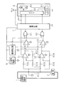
- FIG. 1 is a block diagram showing a configuration example of a current detection circuit according to Embodiment 1 of the present invention.
- the current detection circuit includes amplifiers (corresponding to amplifying units) 31 and 32 that amplify a voltage between both ends of a resistor R12 connected between a high voltage power source (corresponding to a power source) 1 including a high voltage battery and a load 2;
- a saw wave generator (corresponding to a generator) 4 for generating a saw wave signal, and a comparator for comparing the voltage of the saw wave signal generated by the saw wave generator 4 and the voltage amplified by the amplifiers 31 and 32, respectively. 51, 52).
- the sawtooth wave generator 4 may be a triangular wave generator that generates a triangular wave signal.
- the current detection circuit is also an AND circuit (second generation unit) that separately takes a negative logic AND for the second signal from the sawtooth generator 4 (details will be described later) and the output signals of the comparators 51 and 52.
- 61, 62 and the sawtooth wave generator 4 and the AND circuits 61, 62 are electrically insulated from the subsequent circuit and separated, and the input signal is transmitted to the subsequent stage (corresponding to the insulating portion). ) 7, and a microcomputer 8 (corresponding to a detection unit, hereinafter referred to as a microcomputer) 8 that detects a current flowing through the resistor R 12 based on a signal input via the insulation circuit 7.
- the amplifiers 31 and 32, the sawtooth generator 4, the comparators 51 and 52, and the AND circuits 61 and 62 have one end of the resistor R12, that is, one end of the high voltage power supply 1 and the connection point of the resistor R12 as a reference potential.
- Power is supplied from a small signal power supply 9 that generates a power supply voltage with respect to the reference potential.
- the power supply voltage supplied by the small signal power supply 9 is, for example, 5V.
- the other end of the resistor R12 may be set to the reference potential.
- the reference potential becomes low / high with respect to one end of the high-voltage power supply 1.
- the microcomputer 8 and the insulating circuit 7 have the ground potential as a reference potential and are supplied with + 5V Vcc.
- the amplifier 31 includes an analog operational amplifier.
- a resistor R31 is provided between the output terminal and the inverting input terminal, a resistor R32 is provided between the non-inverting input terminal and one end of the resistor R12, and an inverting input terminal and the resistor R12.
- Resistors R33 are respectively connected between the other ends.
- the amplifier 32 includes an operational amplifier, a resistor R34 between the output terminal and the inverting input terminal, a resistor R35 between the non-inverting input terminal and the other end of the resistor R12, and an inverting input terminal and the resistor R12.
- Resistors R36 are respectively connected between the one ends.
- the amplifier 31 operates as an inverting amplifier that inverts and amplifies the negative voltage signal at the other end of the resistor R12 to output a positive voltage signal.
- the amplifier 32 operates as a non-inverting amplifier that amplifies the positive voltage signal at the other end with respect to one end of the resistor R12 without inverting it and outputs a positive voltage signal.
- the output voltage When the amplifiers 31 and 32 are driven by a single power source with respect to the reference potential as in the first embodiment, when the voltage at the other end with respect to one end of the resistor R12 is positive, the output signal of the amplifier 31 When the voltage (hereinafter referred to as the output voltage) is zero and the voltage at the other end with respect to one end of the resistor R12 is negative, the output voltage of the amplifier 32 is zero.
- the resistance value of the resistor R32 is matched with the parallel resistance value of the resistors R31 and R33, and the resistance value of the resistor R35 is the resistance value of the resistors R34 and R34. It is preferable to match the parallel resistance value of R36.
- a publicly known offset compensation circuit may be provided in order to cancel the input offset voltage of each of the amplifiers 31 and 32. Further, a circuit for sampling and holding the voltage across the resistor R21 may be added.
- the output terminals of the amplifiers 31 and 32 are connected to the inverting input terminal, and the sawtooth signal from the sawtooth wave generator 4 is input to the non-inverting input terminal.
- the output signals of the comparators 51 and 52 become L (low) level (or H (high) level).
- each of the AND circuits 61 and 62 the output signals of the comparators 51 and 52 are input to one input terminal, and the second signal from the sawtooth wave generator 4 is input to the other input terminal.
- Each of the AND circuits 61 and 62 represents the comparison result of the comparators 51 and 52 in a period in which the second signal is at L level (corresponding to a period in which the voltage of the signal generated in the generation unit gradually increases or decreases linearly). The signal shown is output.
- the AND circuits 61 and 62 need not be used.
- the comparators 51 and 52 correspond to the comparison unit and the second generation unit.
- the second signal and the output signals of the AND circuits 61 and 62 are respectively input to the timer input terminals of the microcomputer 8 having a so-called input capture function via the insulating circuit 7.
- the second signal is also input to the interrupt input terminal of the microcomputer 8 and generates an interrupt request.
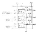
- FIG. 2 is a circuit diagram illustrating a configuration example of the insulating circuit 7.
- the insulation circuit 7 includes photocouplers 71, 72, and 73 including LEDs (Light Emitting Diodes) and phototransistors that are turned on when the LEDs emit light.
- the anode of the LED is connected to the small signal power source 9, and the emitter of the phototransistor is connected to the ground potential.
- Each photocoupler 71, 72, 73 may be replaced with another isolator such as a digital isolator or a pulse transformer.
- the cathode of the LED included in the photocoupler 71 is connected to a sawtooth generator 4 (more specifically, an output terminal of an inverter IV42 to be described later: see FIG. 3) via a resistor R71.
- the cathodes of the LEDs included in the photocouplers 72 and 73 are connected to the output terminals of the AND circuits 61 and 62 via resistors R72 and R73.
- the collector of the phototransistor included in the photocoupler 71 is pulled up to Vcc by the resistor R74, and is connected to the timer input terminal and the interrupt input terminal of the microcomputer 8.
- the collectors of the phototransistors included in the photocouplers 72 and 73 are pulled up to Vcc by resistors R75 and R76 and connected to the timer input terminal of the microcomputer 8.
- each LED when an H level (or L level) signal is input via the input-side resistors R71, 72, 73, each LED does not emit light (or emits light), Since each phototransistor is turned off (or turned on), an H level (or L level) signal is input to the microcomputer 8.
- the microcomputer 8 has a CPU (Central Processing Unit) 81, a timer 82, and an interrupt controller 83, which are mutually connected to a ROM (Read Only Memory) and a RAM (Random Access Memory) (not shown). It is connected.
- the timer 82 includes a first timer, a second timer, and a third timer.
- the first, second, and third timers included in the timer 82 use the count value of a counter that counts a clock (corresponding to a periodic signal) as the falling and rising edges of signals input to the input terminals for the respective timers (
- the signal width is held in the capture register at the leading edge and trailing edge of the signal to be detected) to generate an interrupt request.
- the CPU 81 can accurately detect the signal width of the L level signal by calculating the difference between the count values held in the capture register by an interrupt process.
- the interrupt controller 83 receives the interrupt request from the interrupt input terminal and the interrupt request from the timer 82 and causes the CPU 81 to generate an interrupt.
- the rising edge of the second signal input to the interrupt input terminal is accepted as an interrupt request, but the present invention is not limited to this.
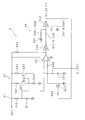
- FIG. 3 is a circuit diagram showing a configuration example of the sawtooth generator 4.
- the sawtooth generator 4 includes a voltage divider 41 composed of resistors R40 and R41 that divides the power supply voltage from the small signal power supply 9, a current mirror circuit 42, and a constant voltage from the small signal power supply 9 via the current mirror circuit 42.
- the capacitor C41 charged with a current
- the comparator 43 that compares the voltage divided by the voltage divider 41 and the voltage of the capacitor C41
- the delay device 44 that delays the rise of the output signal of the comparator 43 are provided.
- the voltage of the capacitor 41 is input to the non-inverting input terminals of the comparators 51 and 52 described above.
- the current mirror circuit 42 includes PNP transistors Q41 and Q42 whose emitters are connected to the small signal power source 9 via resistors R42 and R43, respectively.
- the collector and base of the transistor Q41 and the base of the transistor Q42 are connected to a reference potential via a resistor R44.
- the collector of the transistor Q42 is connected to the other end of the capacitor C41 whose one end is connected to the reference potential.
- the comparator 43 is supplied with power from the small signal power source 9, and the output terminal is pulled up to the small signal power source 9 by the resistor R45.
- the inverting input terminal is connected to the voltage dividing point of the voltage divider 41, and the non-inverting input terminal is connected to the other end of the capacitor C41 via the resistor R46.
- the delay unit 44 includes an inverter IV41 whose input terminal is connected to the output terminal of the comparator 43, a series circuit of a resistor R47 and a capacitor C42 for integrating the output voltage of the inverter IV41, and a connection point between the resistor R47 and the capacitor C42. And a Schmitt trigger type inverter (corresponding to the first generation unit) IV42 to which an input terminal is connected. Connected between the output terminal of the inverter IV41 and the input terminal of the inverter IV42 is a series circuit of a Schottky barrier type diode D41 and a resistor R48 whose cathode is directed to the output terminal side of the inverter IV41.
- the resistance values of the resistors R47 and R48 are 4.7 k ⁇ and 100 ⁇ , for example, and the capacitance value of the capacitor C42 is 470 pF, for example. With this configuration, the fall of the output voltage of the comparator 43 is delayed by the integration circuit of the delay device 44.
- the output signal of the inverter IV42 is the above-described second signal, which is input to one input terminal of the AND circuits 61 and 62 and the input side of the insulating circuit 7, and is an N-channel FET (Field Effect Transistor). Applied to the gate of a certain transistor Q43 via a resistor R49. With this configuration, when the output signal of the comparator 43 becomes H level, the transistor Q43 is turned on and the charge accumulated in the capacitor C41 is discharged.
- FIG. 4 is a timing chart for explaining the operation of the current detection circuit according to the first embodiment of the present invention.
- the seven timing charts shown in FIG. 4 all have the same time axis as the horizontal axis, and the vertical axis shows the voltage of the sawtooth signal (that is, the voltage of the capacitor C41) and the output of the comparator 43 from the upper stage of the figure.
- the level of the signal, the voltage of the capacitor C42, the level of the second signal (ie, the output signal of the inverter IV42), the on / off state of the transistor Q43, the level of the output signal of the comparator 51, and the level of the output signal of the AND circuit 61 Is shown.
- Vth in the figure is a divided voltage of the voltage divider 41, and the peak voltage of the sawtooth signal is Vp.
- the electric charge of the capacitor C41 is rapidly discharged, and the voltage of the sawtooth signal rapidly decreases.
- the voltage of the sawtooth signal immediately before the transistor Q43 is turned on is Vp.
- the increase in the voltage of the capacitor C41 during the period from time t1 to t2 (or from t11 to t12) is negligible compared to Vp.
- the output signal of the comparator 43 falls to L level, and this output signal is inverted to H level by the inverter IV41, so that the capacitor C42 becomes a resistor.
- the battery is gradually charged via R47.
- the output signal (that is, the second signal) of the inverter IV42 falls to the L level, and this signal causes the transistor Q43 turns off. For this reason, charging of the capacitor C41 is started again, and the voltage of the sawtooth signal gradually increases linearly. Note that the electric charge of the capacitor C41 is adjusted so as to be completely discharged during the period from time t2 to t3 (or from t12 to t13).
- the output signal of the amplifier 31 that amplifies the voltage across the resistor R12 is input to the inverting input terminal. Therefore, the output signal changes from the H level to the L level at any time during the period from time t2 to t3 (or from t12 to t13) when the voltage of the sawtooth signal decreases from Vp to 0.
- the output signal of the comparator 51 changes from L level to H level, for example, at time t4 during the period from time t3 to t12 when the voltage of the sawtooth signal increases linearly from 0 to Vp. .
- the output signal of the AND circuit 61 that performs negative logic AND on the second signal and the output signal of the comparator 51 becomes L level at time t3 (or t13), and becomes H level at time t4.
- Time t3 (or t13) is the start point of a period in which the voltage of the sawtooth signal gradually increases linearly. That is, the AND circuit 61 passes the L level signal from the comparator 51 only during the period in which the second signal is at the L level, thereby reducing the falling edge (leading edge) of the signal from the comparator 51 to the active low level. The output is delayed until the leading edge of the second signal.
- T1 be the length of the period during which the second signal is at L level, that is, the period from time t3 to t12 when the voltage of the sawtooth signal increases linearly, and the output signal of the AND circuit 61 is at L level.
- the voltage of the sawtooth signal at time t4 is Vp ⁇ (T2 / T1). Since this voltage is equal to the voltage input to the inverting input terminal of the comparator 51 at time t4, that is, the output voltage of the amplifier 31, the current i flowing from the high voltage power supply 1 to the load 2 via the resistor R12 is as follows: (1).
- T3 When the current i flowing from the load 2 to the high voltage power supply 1 via the resistor R12 is detected, the length T3 of the period during which the output signal of the AND circuit 62 is at the L level is detected, and the equation (1) T2 may be replaced with T3, and ⁇ may be replaced with the absolute value of the amplification factor of the amplifier 32.
- the second signal and the output signal of the AND circuit 61 are individually input to the timer input terminal of the microcomputer 8 via the insulating circuit 7 and are counted by the counter held in the capture register. Based on the difference, T1 and T2 are detected separately. Since T1 and T2 are numerical values used in the expression (1), it is not always necessary to detect them in terms of time.
- T1 and T2 are detected with an accuracy of 1 / f corresponding to the clock cycle.
- the period during which the second signal is at L level, that is, the voltage of the sawtooth signal is linear.
- the length t of the gradually increasing period may be expressed by the following formula (2).
- Factors that decrease the detection accuracy of the current i include voltage fluctuations of the small signal power supply 9, fluctuations in resistance values of the resistors R 40 and R 41 that determine the voltage dividing ratio of the voltage divider 41, and between the high voltage power supply 1 and the load 2. Examples include fluctuations in the resistance value of the connected resistor R12 and fluctuations in the amplification factors of the amplifiers 31 and 32.
- the capacitor C41 whose voltage is the sawtooth signal voltage, the change in capacitance value appears as a change in T1 in equation (1), but T2 also changes at the same rate, so the calculation of equation (1) Does not affect the results.
- the absolute value of the amplification factor of the amplifier 31 is a value of the ratio of the resistance value of the resistor R31 to the resistance value of the resistor R33, and the absolute value of the amplification factor of the amplifier 32 is a resistance value relative to the resistance value of the resistor R36. It is a value obtained by adding 1 to the ratio value of the resistance value of the resistor R34, and it is preferable that the influence of the fluctuation of the resistance value also cancels out these amplification factors.
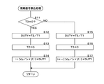
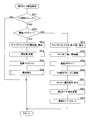
- FIG. 5 is a flowchart showing the processing procedure of the CPU 81 in the periodic signal interrupt process.
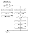
- FIGS. 6, 7 and 8 are respectively a first timer interrupt process, a second timer interrupt process and a third timer interrupt. It is a flowchart which shows the process sequence of CPU81 in a loading process. The interrupt process in FIG. 5 is executed at the rising edge of the second signal.
- the interrupt processing is performed in the capture registers of the first timer, the second timer, and the third timer based on the second signal, the output signal of the AND circuit 61, and the output signal of the AND circuit 62. It is executed when the count value is held.
- Each of r and ⁇ used in the processing of FIG. 5 is the absolute value of the resistance value of the resistor R12 and the amplification factor of the amplifiers 31 and 32 as described above.
- T3 is the length of a period during which the output signal of the AND circuit 62 is at the L level.
- the leading edge flag 1, the leading edge flag 2, and the leading edge flag 3 used in the processes of FIGS. 6, 7, and 8 are flags indicating interrupt processing at the leading edge of the signal whose signal width is to be detected. Yes, and stored in a RAM (not shown).
- T2 and T3 are stored in the RAM with an initial value of 0.
- As for T1 the value detected immediately before is stored in the RAM.
- the current i calculated in the process of FIG. 5 is a positive current that flows from the high-voltage power supply 1 to the load 2 via the resistor R12.
- step S11 the CPU 81 divides T3 by T1 to obtain DUTY (S15), and sets T3 to 0 for the next periodic signal interrupt process (S16). ). Thereafter, the CPU 81 calculates a negative current i by multiplying the result obtained by dividing Vp by r ⁇ ⁇ by DUTY (S17), and returns to the interrupted routine.
- the CPU 81 determines whether or not the leading edge flag 1 is 1 (S21), and when it is 1 (S21: YES), The CPU 81 reads the contents of the capture register as the leading edge value 1 (S22) and stores it in the RAM (S23). Thereafter, the CPU 81 clears the leading edge flag 1 to 0 (S24), and returns to the interrupted routine.
- step S21 the CPU 81 reads the contents of the capture register as the trailing edge value 1 (S25), and the leading edge value stored in the RAM from the trailing edge value 1 T1 is calculated by subtracting 1 (S26). The calculated T1 is stored in the RAM (not shown, and so on). Thereafter, the CPU 81 determines whether or not T1 is greater than a predetermined value (S27). If not (S27: NO), the CPU 81 skips step S28 and returns to the interrupted routine.
- step S27 T1 is compared with the predetermined value because the calculated T1 is the length of the period from time t2 to time t3 shown in FIG. 4 (that is, the period during which the second signal is at the H level). This is because the case T1 is discarded.
- the predetermined value is set to a value smaller than the length of the period from time t3 to t12 and larger than the length of the period from time t2 to t3.
- T1 calculated in the next first timer interrupt process is the length of the period from time t2 to t12, and is larger than the actual T1.
- the length of the period from time t3 to t12 is correctly calculated as T1.
- step S27 If T1 is larger than the predetermined value in step S27 (S27: YES), the CPU 81 sets the leading edge flag 1 to 1 for the next first timer interrupt process (S28), and further the second timer interrupt process. Therefore, the leading edge flag 2 is set to 1 (S29), and the leading edge flag 3 is set to 1 for the third timer interruption process (S30), and the process returns to the interrupted routine.
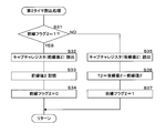
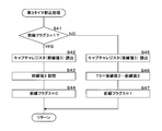
- step S31 to S35 in the second timer interrupt process shown in FIG. 7 are the leading edge flag 1 and the leading edge value 1 in the processes from step S21 to S25 in the first interrupt process shown in FIG. Since each of the trailing edge value 1 is replaced with the leading edge flag 2, the leading edge value 2, and the trailing edge value 2, the description thereof is omitted.
- step S35 the CPU 81 that has read the contents of the capture register as the trailing edge value 2 subtracts the leading edge value 2 stored in the RAM from the trailing edge value 2, and calculates T2 (S36). Thereafter, the CPU 81 sets the leading edge flag 2 to 1 for the next second timer interrupt process (S37), and returns to the interrupted routine.
- step S41 to S45 in the third timer interrupt process shown in FIG. 8 are the leading edge flag 2 and the leading edge value 2 in the processes from step S31 to S35 in the second interrupt process shown in FIG.
- the trailing edge value 2 is replaced with the leading edge flag 3, the leading edge value 3, and the trailing edge value 3, and the description thereof is omitted.
- step S45 the CPU 81, which has read the contents of the capture register as the trailing edge value 3, calculates T3 by subtracting the leading edge value 3 stored in the RAM from the trailing edge value 3 (S46). Thereafter, the CPU 81 sets the leading edge flag 3 to 1 for the next third timer interrupt process (S47), and returns to the interrupted routine.
- the voltage generated between both ends of the resistor R12 connected between one end of the high-voltage power supply 1 and the load 2 is amplified by the amplifiers 31 and 32, and the comparator 51, 52, the lengths T2 and T3 of the signals indicating the comparison results of the comparators 51 and 52 in the slope period in which the voltage of the sawtooth signal increases linearly gradually, and the signal indicating the slope period.
- the current flowing through the resistor R12 is detected based on the ratio of the detected lengths.
- the ratio of the output voltage of the amplifiers 31 and 32 to the peak voltage Vp of the sawtooth signal is calculated, and this ratio, the peak voltage Vp, the absolute value ⁇ of the amplification factor of the amplifiers 31 and 32, and the resistance value of the resistor R12.
- the current value i is detected based on r. Accordingly, it is possible to detect the current with high accuracy and a good step response in a wide dynamic range.
- the timer 82 having a so-called input capture function is supplied with the second signal indicating the slope period and the output signals of the AND circuits 61 and 62 indicating the comparison result.
- the lengths of these signals are detected according to the difference between the count values of the counters held at the leading edge and the trailing edge. Therefore, for example, the length of the signal indicating the slope period and the comparison result are shown in comparison with the case of detecting the time difference by reading the count value of the counter that sequentially changes in the interrupt processing at the leading edge and the trailing edge of the signal. It becomes possible to detect the length of the signal with high accuracy.
- the sawtooth generator 4 and the AND circuits 61 and 62 that generate the signal indicating the slope period and the signal indicating the comparison result, respectively, and the current is detected based on these signals.
- a signal is transmitted from the sawtooth generator 4 and the AND circuits 61 and 62 to the microcomputer 8 while being electrically isolated from the microcomputer 8 by the insulating circuit 7 and separated. Therefore, the current flowing through the resistor R12 can be detected regardless of the reference potential of other circuit parts except the microcomputer 8.
- the current flowing through the resistor R12 can be detected with high accuracy.
- the period in which the voltage in the sawtooth signal gradually increases linearly is defined as the slope period, but the present invention is not limited to this.
- this period may be set as the inclined period.
- the AND circuit 61 passes the L level signal from the comparator 51 only during the period in which the second signal is at the L level, so that the rising edge (rear edge) of the signal from the comparator 51 becomes active low. Output to the trailing edge of the second signal early.
- this period may be a slope period, or the voltage of the sawtooth signal increases gradually.
- both the gradually decreasing periods may be connected to form an inclination period.
- the second signal shown in FIG. 4 may be a thin pulse that rises immediately after time t2.
- the unnecessary AND circuits 61 and 62 may be further reduced and the output signals of the comparators 51 and 52 may be input to the insulation circuit 7.
- the comparators 51 and 52 correspond to the comparison unit and the second generation unit.
- a triangular wave signal may be used instead of the sawtooth wave signal.
- any period of the period in which the voltage of the triangular wave signal gradually increases, the period in which the voltage of the triangular wave signal decreases, and the period in which both periods are connected may be set as the inclined period.
- the first embodiment is a mode in which the output signals of the comparators 51 and 52 are transmitted to the microcomputer 8 via the AND circuits 61 and 62 and the insulating circuit 7
- the modification of the first embodiment is a comparator.
- a signal obtained by ORing the output signals 51 and 52 is transmitted to the microcomputer 8 via the AND circuit 61 and the insulating circuit 7.
- FIG. 9 is a block diagram showing a configuration example of a current detection circuit according to a modification of the first embodiment of the present invention.
- the current detection circuit shown in FIG. 9 has an AND circuit 62 reduced as compared with the current detection circuit shown in FIG. 1 of the first embodiment, and the output signal of the comparators 51 and 52 is a negative logic OR.
- An OR circuit 63 is added, and the output terminal of the OR circuit 63 is connected to one input terminal of the AND circuit 61. Therefore, it is sufficient for the insulating circuit 7 to have two circuits including the two photocouplers 71 and 72, and the timer 82 of the microcomputer 8 may not include the third timer.
- T2 and T3 in the first embodiment are detected without being distinguished from each other, so that the operation of the current detection circuit can be described using the same timing diagram as the timing diagram shown in FIG. Further, in the periodic signal interrupt process shown in FIG. 5, the determination process in step S11 and the processes in steps S15 to S17 are not necessary. Further, the entire third timer interrupt process shown in FIG. 8 is not necessary. Others are the same as those in the first embodiment.
- the first embodiment Has the same effect as.
- the timer 82 of the microcomputer 8 detects the signal widths of the three signals (second signal and output signals of the AND circuits 61 and 62) in parallel. 2 is a mode in which the timer 82 detects the signal widths of the three signals in time series.
- FIG. 10 is a block diagram showing a configuration example of the current detection circuit according to the second embodiment of the present invention.
- the current detection circuit shown in FIG. 10 includes a multiplexer (corresponding to a selection unit, hereinafter referred to as MUX) 85 between the insulation circuit 7 and the microcomputer 8.
- MUX selection unit
- the timer 82 detects the signal width of the signal input to the input terminal for the first timer by the first timer, and the period of the second signal input to the input terminal for the second timer by the second timer. Is detected, or the period for switching the selection of the MUX 85 is counted.
- the timer 82 of the microcomputer 8 may not include the third timer.
- the first timer holds the count value of the counter in the capture register at the falling and rising edges of the signal input to the first timer input terminal and generates an interrupt request.
- the second timer detects the period of the second signal input to the input terminal for the second timer, the second timer holds the count value of the counter in the capture register at the rising edge of the second signal and issues an interrupt request. appear.
- the second timer measures the period, the input capture function is canceled.
- the MUX 85 is supplied with power from Vcc, and selectively switches the signals input to the four selected input terminals according to a combination of 2-bit selection signals from the microcomputer 8, so that the first and the second of the microcomputer 8 are switched. 2 Output to the input terminal for timer.
- the above-mentioned second signal and output signals of the AND circuits 61 and 62 are input to the first to third selected input terminals of the MUX 85 separately via the insulating circuit 7.
- the fourth selected input terminal of the MUX 85 is connected to the ground potential.
- a 2-bit selection signal is input from the output port 84 of the microcomputer 8 to the two selection input terminals of the MUX 85.
- FIG. 11 is a timing chart for explaining the operation of the current detection circuit according to the second embodiment of the present invention.
- Each of the six timing charts shown in FIG. 11 has the same time axis as the horizontal axis, and the vertical axis indicates the level of the second signal, the level of the output signal of the AND circuit 61, and the AND circuit from the top in the figure.
- the 62 shows the level of the output signal 62, the detection phase discrimination by the first timer included in the timer 82, the level of the output signal of the MUX 85, and the operation period of the periodic timer by the second timer included in the timer 82.
- the CPU 81 In each of the T1 detection phase, the T2 detection phase, and the T3 detection phase shown in FIG. 11 as the detection phase by the first timer, the CPU 81 outputs the second signal, the output signal of the AND circuit 61, and the output signal of the AND circuit 62. Represents a phase in which a selection signal is output to select.
- the distinction of the detection phase is stored in a RAM (not shown), and the initial state is the T1 detection phase.
- the second signal is selected from the signals input to the selected input terminal of the MUX 85, and therefore the second timer is detected at the rising edge of the second signal at times t2 and t12.
- the count value of the counter is held in the capture register and an interrupt request is generated.
- the CPU 81 detects the period T0 of the second signal in the interrupt process for this interrupt request.
- the CPU 81 updates the detection phase to the T2 detection phase, and outputs a selection signal from the output port 84 to select the output signal of the AND circuit 61 among the signals input to the selected input terminal of the MUX 85. Further, the CPU 81 starts a period timer having a period T0 using the second timer.
- the count value of the counter of the first timer is held in the capture register at the fall and rise of the second signal at times t3 and t12, and an interrupt request is generated.
- the CPU 81 detects the length T1 of the period during which the second signal is at the L level in the interrupt process for this interrupt request.
- the output signal of the AND circuit 61 is selected from the signals input to the selected input terminal of the MUX 85, the output signal of the AND circuit 61 falls at the falling and rising edges at times t13 and t14.
- the count value of the one-timer counter is held in the capture register and an interrupt request is generated.
- the CPU 81 detects the length T2 of the period during which the output signal of the AND circuit 61 is at the L level in the interrupt process for this interrupt request.
- the CPU 81 updates the detection phase to the T3 detection phase and interrupts the MUX 85 in response to the interrupt process for the interrupt request.
- a selection signal is output from the output port 84 in order to select the output signal of the AND circuit 62 among the signals input to the selection input terminal. Further, the CPU 81 restarts the period timer having the period T0 using the second timer.
- the output signal of the AND circuit 62 is selected from the signals input to the selected input terminal of the MUX 85. However, in the second embodiment, this output signal is maintained at the H level. The length T3 of the period in which the output signal of the AND circuit 62 is at the L level is not detected. Nevertheless, when the period timer by the second timer expires at time t32, the CPU 81 can end the T3 detection phase at time t32.
- the CPU 81 updates the detection phase to the T1 detection phase in the interrupt processing for the interrupt request, and then the second timer Change to the input capture setting.
- the CPU 81 further selects a ground potential signal from the signals input to the selected input terminal of the MUX 85 for a very short time, and then outputs a selection signal from the output port 84 to select the second signal.
- the output signal of the MUX 85 always rises at time t32. That is, in the T1 detection phase after time t32, exactly the same operation as in the T1 detection phase after time t2 is repeated.
- FIG. 12 is a flowchart showing the processing procedure of the CPU 81 in the second timer interrupt process
- FIG. 13 is a flowchart showing the processing procedure of the CPU 81 in the periodic timer interrupt process
- FIG. 14 shows the first timer interrupt process
- FIG. 15 is a flowchart showing the processing procedure of the CPU 81 relating to the leading edge value / rear edge value reading subroutine.
- the interrupt processing of FIGS. 12 and 14 is executed when the count values are held in the capture registers of the second timer and the first timer, respectively.
- the interrupt process of FIG. 13 is executed when the period timer by the second timer is up.
- the start flag used in the processing of FIG. 12 is a flag indicating that it is an interrupt processing at the start of a signal whose cycle is to be detected, and is stored in a RAM (not shown).
- the leading edge flag used in the processing of FIG. 14 is a flag indicating that the interrupt processing is performed at the leading edge of the signal whose signal width is to be detected, and is stored in the RAM.
- the detection phase distinction is also stored in the RAM.
- T2 and T3 are stored in the RAM with an initial value of 0. As for T1, the value detected immediately before is stored in the RAM.
- the second timer is set for input capture.
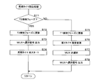
- the CPU 81 determines whether or not the current time is the T1 detection phase (S51), and if it is not the T1 detection phase (S51: NO), nothing is processed. Return to the interrupted routine without.
- the CPU 81 determines whether or not the start flag is 1 (S52), and when it is 1 (S52: YES), the contents of the capture register are changed. It is read as a start value (S53) and stored in the RAM (S54).
- the CPU 81 clears the leading edge flag to 0 (S55), calls and executes a subroutine relating to current detection (S56), and then returns to the interrupted routine.
- the processing content of the subroutine relating to current detection is to detect the current i based on T1, T2, and T3 detected before time t2, and the periodic signal interrupt shown in FIG. 5 of the first embodiment. Since the contents of steps S11 to S17 in the process are exactly the same, the illustration of the flowchart and the description thereof are omitted.
- step S52 If the start flag is not 1 in step S52 (S52: NO), the CPU 81 reads the contents of the capture register as the end value (S57), and subtracts the start value stored in the RAM from the end value to calculate T0. (S58). The calculated T0 is stored in the RAM (not shown, and so on). Thereafter, the CPU 81 sets the start flag to 1 for the next second timer interrupt process (S59), updates the detection phase to the T2 detection phase (S60), and then inputs the selected input terminal of the MUX85. A selection signal is output from the output port 84 in order to select the output signal of the AND circuit 61 among the signals to be output (S61).
- the CPU 81 changes the setting of the second timer to cancel the input capture setting (S62), starts the periodic timer by the second timer (S63), and returns to the interrupted routine.
- the period set in the period timer is T0 calculated in step S58.
- the CPU 81 determines whether or not the current time is the T2 detection phase (S71), and if it is the T2 detection phase (S71: YES), The detection phase is updated to the T3 detection phase (S72). Thereafter, the CPU 81 outputs a selection signal from the output port 84 to select the output signal of the AND circuit 62 among the signals input to the selected input terminal of the MUX 85 (S73), and restarts the periodic timer by the second timer. (S74) and return to the interrupted routine.
- step S71 if the current time is not the T2 detection phase (S71: NO), that is, if it is the T3 detection phase, the CPU 81 updates the detection phase to the T1 detection phase (S75), and then inputs the second timer again. The setting is changed to (S76). Further, the CPU 81 once deselects the MUX 85 (S77), and then outputs a selection signal from the output port 84 to select the second signal among the signals input to the selected input terminal of the MUX 85 ( In step S78, the process returns to the interrupted routine.
- the CPU 81 determines whether or not the current time is the T1 detection phase (S81), and if it is the T1 detection phase (S81: YES). Then, a subroutine relating to reading of the leading edge value / rear edge value is called and executed (S82), Tx calculated in the subroutine is substituted into T1 (S83), and the process returns to the interrupted routine.
- step S81 when the current time is not the T1 detection phase (S81: NO), the CPU 81 determines whether or not the current time is the T2 detection phase (S84), and when the current time is the T2 detection phase (S84: YES), A subroutine relating to reading of the leading edge value and trailing edge value is called and executed (S85), Tx calculated in the subroutine is substituted into T2 (S86), and the process returns to the interrupted routine.
- step S84 if the current time is not the T2 detection phase (S84: NO), that is, if it is the T3 detection phase, the CPU 81 calls and executes a subroutine relating to reading of the leading edge value / rear edge value (S87). Substituting Tx calculated in step T3 (S88), the process returns to the interrupted routine.
- the CPU 81 determines whether or not the leading edge flag is 1 (S91). When the leading edge flag is 1 (S91: YES), the CPU 81 reads the contents of the capture register as a leading edge value (S92), stores it in the RAM (S93), and clears the leading edge flag to 0 (S94). ) Return to the called routine.
- step S91 the CPU 81 reads the contents of the capture register as a trailing edge value (S95), and subtracts the leading edge value stored in the RAM from the trailing edge value. Tx is calculated (S96). The calculated Tx is stored in the RAM (not shown). Thereafter, the CPU 81 sets the leading edge flag to 1 (S97) and returns to the called routine.
- the signal indicating the inclination period and the signal indicating the comparison result are selectively switched by the MUX 85 and transmitted from the sawtooth generator 4 and the AND circuits 61 and 62 to the microcomputer 8. To do.
- This switching is performed according to the signal period T0 when the signal indicating the tilt period is transmitted. Therefore, it is possible to detect the signal width of the signal indicating the tilt period and the signal width of the signal indicating the comparison result in time series, and the number of timers used in the microcomputer 8 is reduced by one.
- the signal width is not detected while the signal indicating the comparison result is transmitted, it is possible to detect a current having a value of 0 corresponding to a signal width of 0.
Abstract
Provided is a current detection circuit that can detect current in a wide dynamic range, with high precision, and with a good step response. Voltage that is generated between both ends of a resistor (R12) connected between a high-voltage power supply (1) and a load (2) is amplified by amplifiers (31, 32) and compared, by comparators (51, 52), to the voltage of a saw-tooth wave signal; the lengths T2, T3 of signals indicating the comparison results from the comparators (51, 52) during an inclined period in which the voltage of the saw-tooth wave signal linearly and gradually increases or decreases and the length T1 of the inclined period are detected; and the current flowing to the resistor (R12) is detected on the basis of the ratio between the detected lengths.
Description
本発明は、電源及び負荷の間で抵抗器を介して流れる電流を検出する電流検出回路に関する。
The present invention relates to a current detection circuit that detects a current flowing between a power source and a load via a resistor.
従来、バッテリ、モータ等の負荷に流れる電流を検出する方法が数多く提案されている。一般的に直流電流を検出するための電流センサには、ホール素子又はシャント抵抗器が用いられている。電流センサによるアナログの検出結果は、必要に応じてデジタル値に変換される。
Conventionally, many methods for detecting the current flowing through a load such as a battery or a motor have been proposed. In general, a Hall element or a shunt resistor is used as a current sensor for detecting a direct current. The analog detection result by the current sensor is converted into a digital value as necessary.
例えば、特許文献1には、車両のバッテリが充放電する電流の値を、ホール素子を備える電流センサで検出する制御装置が記載されている。この電流センサは鉄心を有しており、残留磁気及びヒステリシスの影響で検出結果にオフセット誤差が含まれるため、特許文献1では、電流センサによる検出結果がオフセット補正装置で補正されるようになっている。
For example, Patent Document 1 describes a control device that detects a value of a current charged / discharged by a vehicle battery by a current sensor including a Hall element. Since this current sensor has an iron core and an offset error is included in the detection result due to the influence of residual magnetism and hysteresis, in Patent Document 1, the detection result by the current sensor is corrected by the offset correction device. Yes.
一方、電流センサによる検出結果をA/D変換してデジタル値に変換する場合、例えばマイコン内蔵のA/D変換器ではビット数が不足することがあり、外付けの高価なA/D変換器を用いずに高精度に電流を検出してデジタル値に変換することが望まれる。
On the other hand, when the result detected by the current sensor is converted into a digital value by A / D conversion, for example, an A / D converter with a built-in microcomputer may have insufficient bits, and an externally expensive A / D converter It is desired to detect the current with high accuracy and convert it to a digital value without using the.
これに対し、特許文献2には、PMモータ(永久磁石電動機)に流れる電流を電流センサで検出し、検出結果をΔΣ(デルタ・シグマ)変調器で1ビット信号(ビットストリーム)に変換するモータ制御装置が記載されている。
In contrast, Patent Document 2 discloses a motor that detects a current flowing in a PM motor (permanent magnet motor) with a current sensor and converts the detection result into a 1-bit signal (bit stream) with a ΔΣ (delta sigma) modulator. A control device is described.
しかしながら、特許文献1に記載のホール素子を備える電流センサは、広いダイナミックレンジで高精度に電流を検出することが難しく、構造が複雑で比較的高価であるという問題があった。また、特許文献2に記載のΔΣ変調器は、逐次比較方式のA/D変換器と比較して、オーバーサンプリングを行うために消費電力が大きく、且つステップ応答に劣るために変換のセトリング時間が長いという問題があった。
However, the current sensor including the Hall element described in Patent Document 1 has a problem that it is difficult to detect current with high accuracy in a wide dynamic range, and the structure is complicated and relatively expensive. In addition, the ΔΣ modulator described in Patent Document 2 consumes a large amount of power for performing oversampling and is inferior to a step response compared to a successive approximation type A / D converter, so that the settling time for conversion is large. There was a problem of being long.
本発明は斯かる事情に鑑みてなされたものであり、その目的とするところは、広いダイナミックレンジで高精度に、且つ良好なステップ応答で電流を検出することが可能な電流検出回路を提供することにある。
The present invention has been made in view of such circumstances, and an object of the present invention is to provide a current detection circuit capable of detecting a current with a wide dynamic range with high accuracy and a good step response. There is.
本発明の一態様に係る電流検出回路は、電源及び負荷の間で抵抗器を介して流れる電流を検出する電流検出回路において、三角波信号又は鋸波信号を発生する発生部と、該発生部で発生する信号の電圧が直線的に漸増又は漸減する期間を示す信号を生成する第1生成部と、前記抵抗器の両端間の電圧を増幅する増幅部と、該増幅部で増幅した信号の電圧及び前記発生部で発生した電圧を比較する比較部と、前記期間における前記比較部の比較結果を示す信号を生成する第2生成部と、前記第1生成部からの信号の信号幅に対する前記第2生成部からの信号の信号幅の比に基づいて前記抵抗器に流れる電流を検出する検出部とを備えることを特徴とする。
A current detection circuit according to one embodiment of the present invention includes a generation unit that generates a triangular wave signal or a sawtooth wave signal in a current detection circuit that detects a current flowing through a resistor between a power supply and a load, and the generation unit A first generator for generating a signal indicating a period in which the voltage of the generated signal linearly increases or decreases linearly; an amplifier for amplifying a voltage between both ends of the resistor; and a voltage of the signal amplified by the amplifier And a comparator that compares the voltages generated in the generator, a second generator that generates a signal indicating a comparison result of the comparator in the period, and the signal width of the signal from the first generator. And a detection unit that detects a current flowing through the resistor based on a ratio of signal widths of signals from the two generation units.
本発明の一態様に係る電流検出回路は、前記検出部は、周期信号を計数するカウンタの計数値を、信号幅を検知すべき信号の前縁及び後縁で保持して差分をとることにより、前記第1及び第2生成部夫々からの信号の信号幅を検知することを特徴とする。
In the current detection circuit according to one aspect of the present invention, the detection unit holds a count value of a counter that counts a periodic signal at a leading edge and a trailing edge of a signal whose signal width is to be detected, and obtains a difference. The signal widths of the signals from the first and second generation units are detected.
本発明の一態様に係る電流検出回路は、前記第1及び第2生成部と前記検出部とを電気的に絶縁して前記第1及び第2生成部から前記検出部に信号を伝達する絶縁部を備えることを特徴とする。
The current detection circuit according to an aspect of the present invention is an insulating circuit that electrically insulates the first and second generation units and the detection unit and transmits a signal from the first and second generation units to the detection unit. It comprises a part.
本発明の一態様に係る電流検出回路は、前記抵抗器の端子の何れか一方の電位を、前記第1及び第2生成部の基準電位とすることを特徴とする。
The current detection circuit according to an aspect of the present invention is characterized in that the potential of any one of the terminals of the resistor is set as a reference potential of the first and second generation units.
本発明の一態様に係る電流検出回路は、前記第1及び第2生成部からの信号を選択的に切り替えて前記検出部に伝達する選択部を備え、前記検出部は、前記選択部を介して伝達された前記第1生成部からの信号の周期に応じて前記選択部を切り替えることを特徴とする。
A current detection circuit according to an aspect of the present invention includes a selection unit that selectively switches signals from the first and second generation units and transmits the signals to the detection unit, and the detection unit is configured to pass through the selection unit. The selection unit is switched according to the cycle of the signal from the first generation unit transmitted in the above.
本態様にあっては、電源及び負荷の間に接続された抵抗器の両端間に生じる電圧を増幅部で増幅して鋸波信号又は三角波信号の電圧と比較し、鋸波信号又は三角波信号の電圧が直線的に漸増又は漸減する傾斜期間における比較結果を示す信号の長さと、上記傾斜期間を示す信号の長さとを検知し、検知した長さの比率に基づいて上記抵抗器に流れる電流を検出する。
これにより、鋸波信号又は三角波信号のピーク電圧に対する増幅部の出力電圧の比率が算出され、この比率と、上記ピーク電圧の値、増幅部の増幅率及び抵抗器の抵抗値とに基づいて電流値が検出される。 In this aspect, the voltage generated between both ends of the resistor connected between the power source and the load is amplified by the amplifying unit and compared with the voltage of the sawtooth signal or the triangular wave signal. The length of the signal indicating the comparison result in the ramp period in which the voltage gradually increases or decreases linearly and the length of the signal indicating the tilt period are detected, and the current flowing through the resistor is determined based on the ratio of the detected length. To detect.
Thereby, the ratio of the output voltage of the amplifying unit to the peak voltage of the sawtooth signal or the triangular wave signal is calculated, and based on this ratio, the value of the peak voltage, the amplification factor of the amplifying unit, and the resistance value of the resistor A value is detected.
本態様にあっては、例えば所謂インプットキャプチャ機能を有するタイマに上記傾斜期間を示す信号及び上記比較結果を示す信号を入力し、夫々の信号の前縁及び後縁で保持されたカウンタの計数値の差分に応じてこれらの信号の長さを検知する。
これにより、例えば信号の前縁及び後縁における割込処理で逐次変化するカウンタの計数値を読み出して時間差を検知する場合と比較して、上記傾斜期間を示す信号の長さ及び上記比較結果を示す信号の長さが高精度に検知される。 In this embodiment, for example, a signal indicating the slope period and a signal indicating the comparison result are input to a timer having a so-called input capture function, and the count value of the counter held at the leading edge and the trailing edge of each signal. The lengths of these signals are detected according to the difference between them.
Thereby, for example, compared with the case of detecting the time difference by reading the count value of the counter that sequentially changes in the interrupt processing at the leading edge and the trailing edge of the signal, the length of the signal indicating the slope period and the comparison result are obtained. The length of the indicated signal is detected with high accuracy.
本態様にあっては、上記傾斜期間を示す信号及び上記比較結果を示す信号を生成する生成回路部分と、これらの信号に基づいて電流を検出する検出回路部分とを電気的に絶縁して分離しつつ、上記生成回路部分から上記検出回路部分に信号を伝達する。
これにより、上記検出回路部分を除くその他の回路部分の基準電位の如何にかかわらず、上記抵抗器に流れる電流が検出される。 In this aspect, the generation circuit portion that generates the signal indicating the inclination period and the signal indicating the comparison result and the detection circuit portion that detects current based on these signals are electrically insulated and separated. However, a signal is transmitted from the generation circuit portion to the detection circuit portion.
As a result, the current flowing through the resistor is detected regardless of the reference potential of the other circuit portions except the detection circuit portion.
本態様にあっては、抵抗器の両端のうちの何れか一方の電位を基準電位として、上記傾斜期間を示す信号及び上記比較結果を示す信号を生成する。
これにより、上記抵抗器の両端間の微少な電圧が低ノイズで安定に増幅されるため、上記抵抗器に流れる電流が高精度に検出される。 In this aspect, a signal indicating the tilt period and a signal indicating the comparison result are generated using the potential of either one of both ends of the resistor as a reference potential.
As a result, a minute voltage across the resistor is stably amplified with low noise, so that the current flowing through the resistor is detected with high accuracy.
本態様にあっては、上記傾斜期間を示す信号及び上記比較結果を示す信号を選択的に切り替えて上記生成回路部分から検出回路部分に伝達する。この切り替えは、上記傾斜期間を示す信号が伝送されているときの信号周期に応じて行われる。
これにより、上記傾斜期間を示す信号の信号幅及び上記比較結果を示す信号の信号幅が時系列的に検知される。また、上記比較結果を示す信号が伝達されている間に信号幅が検知されない場合は、値が0の信号幅に対応して値が0の電流が検出される。 In this aspect, the signal indicating the tilt period and the signal indicating the comparison result are selectively switched and transmitted from the generation circuit portion to the detection circuit portion. This switching is performed according to the signal cycle when the signal indicating the tilt period is transmitted.
Thereby, the signal width of the signal indicating the tilt period and the signal width of the signal indicating the comparison result are detected in time series. When the signal width is not detected while the signal indicating the comparison result is transmitted, a current having a value of 0 is detected corresponding to the signal width of 0.
上記によれば、鋸波信号又は三角波信号のピーク電圧に対する増幅部の出力電圧の比率が算出され、この比率と、上記ピーク電圧の値、増幅部の増幅率及び抵抗値とに基づいて、時間遅れを伴うフィードバック無しに電流値が検出される。
従って、広いダイナミックレンジで高精度に、且つ良好なステップ応答で電流を検出することが可能となる。 According to the above, the ratio of the output voltage of the amplifying unit to the peak voltage of the sawtooth signal or the triangular wave signal is calculated, and based on this ratio, the value of the peak voltage, the amplification factor of the amplifying unit, and the resistance value, the time The current value is detected without feedback with delay.
Accordingly, it is possible to detect the current with high accuracy and a good step response in a wide dynamic range.
以下、本発明をその実施の形態を示す図面に基づいて詳述する。
(実施の形態1)
図1は、本発明の実施の形態1に係る電流検出回路の構成例を示すブロック図である。電流検出回路は、高圧のバッテリを含む高電圧電源(電源に相当)1及び負荷2の間に接続された抵抗器R12の両端間の電圧を増幅する増幅器(増幅部に相当)31,32と、鋸波信号を発生する鋸波発生器(発生部に相当)4と、鋸波発生器4が発生した鋸波信号の電圧及び増幅器31,32が増幅した電圧を各別に比較する比較器(比較部に相当)51,52とを備える。鋸波発生器4は、三角波信号を発生する三角波発生器であってもよい。 Hereinafter, the present invention will be described in detail with reference to the drawings illustrating embodiments thereof.
(Embodiment 1)
FIG. 1 is a block diagram showing a configuration example of a current detection circuit according to Embodiment 1 of the present invention. The current detection circuit includes amplifiers (corresponding to amplifying units) 31 and 32 that amplify a voltage between both ends of a resistor R12 connected between a high voltage power source (corresponding to a power source) 1 including a high voltage battery and aload 2; A saw wave generator (corresponding to a generator) 4 for generating a saw wave signal, and a comparator for comparing the voltage of the saw wave signal generated by the saw wave generator 4 and the voltage amplified by the amplifiers 31 and 32, respectively. 51, 52). The sawtooth wave generator 4 may be a triangular wave generator that generates a triangular wave signal.
(実施の形態1)
図1は、本発明の実施の形態1に係る電流検出回路の構成例を示すブロック図である。電流検出回路は、高圧のバッテリを含む高電圧電源(電源に相当)1及び負荷2の間に接続された抵抗器R12の両端間の電圧を増幅する増幅器(増幅部に相当)31,32と、鋸波信号を発生する鋸波発生器(発生部に相当)4と、鋸波発生器4が発生した鋸波信号の電圧及び増幅器31,32が増幅した電圧を各別に比較する比較器(比較部に相当)51,52とを備える。鋸波発生器4は、三角波信号を発生する三角波発生器であってもよい。 Hereinafter, the present invention will be described in detail with reference to the drawings illustrating embodiments thereof.
(Embodiment 1)
FIG. 1 is a block diagram showing a configuration example of a current detection circuit according to Embodiment 1 of the present invention. The current detection circuit includes amplifiers (corresponding to amplifying units) 31 and 32 that amplify a voltage between both ends of a resistor R12 connected between a high voltage power source (corresponding to a power source) 1 including a high voltage battery and a
電流検出回路は、また、鋸波発生器4からの第2の信号(詳細については後述する)及び比較器51,52の出力信号について負論理のANDを各別にとるAND回路(第2生成部に相当)61,62と、鋸波発生器4及びAND回路61,62を後段の回路から電気的に絶縁して分離しつつ、入力された信号を後段に伝達する絶縁回路(絶縁部に相当)7と、絶縁回路7を介して入力された信号に基づいて抵抗器R12に流れる電流を検出するマイクロコンピュータ(検出部に相当、以下マイコンという)8とを備える。
The current detection circuit is also an AND circuit (second generation unit) that separately takes a negative logic AND for the second signal from the sawtooth generator 4 (details will be described later) and the output signals of the comparators 51 and 52. 61, 62 and the sawtooth wave generator 4 and the AND circuits 61, 62 are electrically insulated from the subsequent circuit and separated, and the input signal is transmitted to the subsequent stage (corresponding to the insulating portion). ) 7, and a microcomputer 8 (corresponding to a detection unit, hereinafter referred to as a microcomputer) 8 that detects a current flowing through the resistor R 12 based on a signal input via the insulation circuit 7.
増幅器31,32、鋸波発生器4、比較器51,52及びAND回路61,62は、抵抗器R12の一端、即ち高電圧電源1の一端及び抵抗器R12の接続点を基準電位としており、この基準電位に対する電源電圧を発生する小信号電源9から電源が供給されている。小信号電源9が供給する電源の電圧は、例えば5Vである。ここでは、抵抗器R12の他端を基準電位にしてもよいが、抵抗器R12に流れる電流が大/小に変化したときに、基準電位が高電圧電源1の一端に対して低/高に変動することに不都合がある場合は、抵抗器R12の一端を基準電位とすることが好ましい。マイコン8及び絶縁回路7は、接地電位を基準電位としており、+5VのVccが供給されている。
The amplifiers 31 and 32, the sawtooth generator 4, the comparators 51 and 52, and the AND circuits 61 and 62 have one end of the resistor R12, that is, one end of the high voltage power supply 1 and the connection point of the resistor R12 as a reference potential. Power is supplied from a small signal power supply 9 that generates a power supply voltage with respect to the reference potential. The power supply voltage supplied by the small signal power supply 9 is, for example, 5V. Here, the other end of the resistor R12 may be set to the reference potential. However, when the current flowing through the resistor R12 changes to large / small, the reference potential becomes low / high with respect to one end of the high-voltage power supply 1. When there is an inconvenience in the fluctuation, it is preferable to set one end of the resistor R12 as a reference potential. The microcomputer 8 and the insulating circuit 7 have the ground potential as a reference potential and are supplied with + 5V Vcc.
増幅器31は、アナログの演算増幅器を含み、出力端子及び反転入力端子の間に抵抗器R31が、非反転入力端子及び抵抗器R12の一端の間に抵抗器R32が、反転入力端子及び抵抗器R12の他端の間に抵抗器R33が夫々接続されている。増幅器32は、演算増幅器を含み、出力端子及び反転入力端子の間に抵抗器R34が、非反転入力端子及び抵抗器R12の他端の間に抵抗器R35が、反転入力端子及び抵抗器R12の一端の間に抵抗器R36が夫々接続されている。
The amplifier 31 includes an analog operational amplifier. A resistor R31 is provided between the output terminal and the inverting input terminal, a resistor R32 is provided between the non-inverting input terminal and one end of the resistor R12, and an inverting input terminal and the resistor R12. Resistors R33 are respectively connected between the other ends. The amplifier 32 includes an operational amplifier, a resistor R34 between the output terminal and the inverting input terminal, a resistor R35 between the non-inverting input terminal and the other end of the resistor R12, and an inverting input terminal and the resistor R12. Resistors R36 are respectively connected between the one ends.
これにより、増幅器31は、抵抗器R12の一端に対する他端の負の電圧信号を反転増幅して正の電圧信号を出力する反転増幅器として動作する。また、増幅器32は、抵抗器R12の一端に対する他端の正の電圧信号を反転せずに増幅して正の電圧信号を出力する非反転増幅器として動作する。なお、本実施の形態1のように、増幅器31及び32を基準電位に対する単一電源で駆動する場合、抵抗器R12の一端に対する他端の電圧が正であるときは、増幅器31の出力信号の電圧(以下、出力電圧という)が0となり、抵抗器R12の一端に対する他端の電圧が負であるときは、増幅器32の出力電圧が0となる。
Thus, the amplifier 31 operates as an inverting amplifier that inverts and amplifies the negative voltage signal at the other end of the resistor R12 to output a positive voltage signal. The amplifier 32 operates as a non-inverting amplifier that amplifies the positive voltage signal at the other end with respect to one end of the resistor R12 without inverting it and outputs a positive voltage signal. When the amplifiers 31 and 32 are driven by a single power source with respect to the reference potential as in the first embodiment, when the voltage at the other end with respect to one end of the resistor R12 is positive, the output signal of the amplifier 31 When the voltage (hereinafter referred to as the output voltage) is zero and the voltage at the other end with respect to one end of the resistor R12 is negative, the output voltage of the amplifier 32 is zero.
ここでは、増幅器31及び32夫々の入力オフセット電流を打ち消すために、抵抗器R32の抵抗値は、抵抗器R31及びR33の並列抵抗値と一致させ、抵抗器R35の抵抗値は、抵抗器R34及びR36の並列抵抗値と一致させることが好ましい。また、増幅器31及び32夫々の入力オフセット電圧を打ち消すために、それ自体公知のオフセット補償回路を設けてもよい。更に、抵抗器R21の両端間の電圧をサンプル&ホールドする回路を追加してもよい。
Here, in order to cancel the input offset current of each of the amplifiers 31 and 32, the resistance value of the resistor R32 is matched with the parallel resistance value of the resistors R31 and R33, and the resistance value of the resistor R35 is the resistance value of the resistors R34 and R34. It is preferable to match the parallel resistance value of R36. Further, in order to cancel the input offset voltage of each of the amplifiers 31 and 32, a publicly known offset compensation circuit may be provided. Further, a circuit for sampling and holding the voltage across the resistor R21 may be added.
比較器51及び52の夫々は、反転入力端子に増幅器31及び32の出力端子が接続されており、非反転入力端子に鋸波発生器4からの鋸波信号が入力されている。これにより、鋸波信号の電圧が増幅器31及び32夫々の出力電圧を下回る場合(又は上回る場合)、比較器51及び52の出力信号がL(ロウ)レベル(又はH(ハイ)レベル)となる。
In each of the comparators 51 and 52, the output terminals of the amplifiers 31 and 32 are connected to the inverting input terminal, and the sawtooth signal from the sawtooth wave generator 4 is input to the non-inverting input terminal. Thereby, when the voltage of the sawtooth signal is lower (or higher) than the output voltage of each of the amplifiers 31 and 32, the output signals of the comparators 51 and 52 become L (low) level (or H (high) level). .
AND回路61及び62の夫々は、一の入力端子に比較器51及び52の出力信号が入力されており、他の入力端子に鋸波発生器4からの第2の信号が入力されている。AND回路61及び62の夫々は、第2の信号がLレベルである期間(発生部で発生する信号の電圧が直線的に漸増又は漸減する期間に相当)における比較器51及び52の比較結果を示す信号を出力する。
In each of the AND circuits 61 and 62, the output signals of the comparators 51 and 52 are input to one input terminal, and the second signal from the sawtooth wave generator 4 is input to the other input terminal. Each of the AND circuits 61 and 62 represents the comparison result of the comparators 51 and 52 in a period in which the second signal is at L level (corresponding to a period in which the voltage of the signal generated in the generation unit gradually increases or decreases linearly). The signal shown is output.
鋸波信号の立ち下がり時間が無視できる場合は、AND回路61及び62を用いなくてもよい。この場合は、比較器51,52が比較部及び第2生成部に相当する。上記第2の信号及びAND回路61,62の出力信号は、絶縁回路7を介して、所謂インプットキャプチャ機能を有するマイコン8のタイマ用の入力端子に各別に入力される。マイコン8のタイマ用の入力端子に入力される信号のうち、第2の信号は、マイコン8の割込用の入力端子にも入力されており、割込要求を発生する。
When the falling time of the sawtooth signal can be ignored, the AND circuits 61 and 62 need not be used. In this case, the comparators 51 and 52 correspond to the comparison unit and the second generation unit. The second signal and the output signals of the AND circuits 61 and 62 are respectively input to the timer input terminals of the microcomputer 8 having a so-called input capture function via the insulating circuit 7. Of the signals input to the timer input terminal of the microcomputer 8, the second signal is also input to the interrupt input terminal of the microcomputer 8 and generates an interrupt request.
ここで、絶縁回路7について説明する。
図2は、絶縁回路7の構成例を示す回路図である。絶縁回路7は、LED(Light Emitting Diode )及び該LEDが発光したときにオンするフォトトランジスタを含むフォトカプラ71,72,73を有する。各フォトカプラ71,72,73について、LEDのアノードは小信号電源9に接続されており、フォトトランジスタのエミッタは接地電位に接続されている。各フォトカプラ71,72,73は、デジタルアイソレータ、パルストランス等の他のアイソレータに置き換えてもよい。 Here, the insulatingcircuit 7 will be described.
FIG. 2 is a circuit diagram illustrating a configuration example of the insulatingcircuit 7. The insulation circuit 7 includes photocouplers 71, 72, and 73 including LEDs (Light Emitting Diodes) and phototransistors that are turned on when the LEDs emit light. For each of the photocouplers 71, 72, 73, the anode of the LED is connected to the small signal power source 9, and the emitter of the phototransistor is connected to the ground potential. Each photocoupler 71, 72, 73 may be replaced with another isolator such as a digital isolator or a pulse transformer.
図2は、絶縁回路7の構成例を示す回路図である。絶縁回路7は、LED(Light Emitting Diode )及び該LEDが発光したときにオンするフォトトランジスタを含むフォトカプラ71,72,73を有する。各フォトカプラ71,72,73について、LEDのアノードは小信号電源9に接続されており、フォトトランジスタのエミッタは接地電位に接続されている。各フォトカプラ71,72,73は、デジタルアイソレータ、パルストランス等の他のアイソレータに置き換えてもよい。 Here, the insulating
FIG. 2 is a circuit diagram illustrating a configuration example of the insulating
フォトカプラ71に含まれるLEDのカソードは、抵抗器R71を介して鋸波発生器4(より詳しくは後述するインバータIV42の出力端子:図3参照)に接続されている。フォトカプラ72及び73夫々に含まれるLEDのカソードは、抵抗器R72及びR73を介してAND回路61及び62の出力端子に接続されている。フォトカプラ71に含まれるフォトトランジスタのコレクタは、抵抗器R74によりVccにプルアップされると共にマイコン8のタイマ用の入力端子及び割込用の入力端子に接続されている。フォトカプラ72及び73夫々に含まれるフォトトランジスタのコレクタは、抵抗器R75及び76によりVccにプルアップされると共にマイコン8のタイマ用の入力端子に接続されている。
The cathode of the LED included in the photocoupler 71 is connected to a sawtooth generator 4 (more specifically, an output terminal of an inverter IV42 to be described later: see FIG. 3) via a resistor R71. The cathodes of the LEDs included in the photocouplers 72 and 73 are connected to the output terminals of the AND circuits 61 and 62 via resistors R72 and R73. The collector of the phototransistor included in the photocoupler 71 is pulled up to Vcc by the resistor R74, and is connected to the timer input terminal and the interrupt input terminal of the microcomputer 8. The collectors of the phototransistors included in the photocouplers 72 and 73 are pulled up to Vcc by resistors R75 and R76 and connected to the timer input terminal of the microcomputer 8.
上述の構成を有する絶縁回路7において、入力側の抵抗器R71,72,73を介してHレベル(又はLレベル)の信号が入力された場合、各LEDが発光せず(又は発光し)、各フォトトランジスタがオフする(又はオンする)ため、マイコン8にHレベル(又はLレベル)の信号が入力される。
In the insulating circuit 7 having the above-described configuration, when an H level (or L level) signal is input via the input-side resistors R71, 72, 73, each LED does not emit light (or emits light), Since each phototransistor is turned off (or turned on), an H level (or L level) signal is input to the microcomputer 8.
図1に戻って、マイコン8は、CPU(Central Processing Unit )81、タイマ82及び割込コントローラ83を有し、これらが不図示のROM(Read Only Memory )及びRAM(Random Access Memory )と共に互いにバス接続されている。タイマ82には、第1タイマ、第2タイマ及び第3タイマが含まれている。
Returning to FIG. 1, the microcomputer 8 has a CPU (Central Processing Unit) 81, a timer 82, and an interrupt controller 83, which are mutually connected to a ROM (Read Only Memory) and a RAM (Random Access Memory) (not shown). It is connected. The timer 82 includes a first timer, a second timer, and a third timer.
タイマ82に含まれる第1、第2及び第3タイマは、クロック(周期信号に相当)を計数するカウンタの計数値を、夫々のタイマ用の入力端子に入力された信号の立ち下がり及び立ち上がり(信号幅を検知すべき信号の前縁及び後縁に相当)でキャプチャレジスタに保持して割込要求を発生する。CPU81は、キャプチャレジスタに保持された計数値の差分を割込処理で算出して、Lレベルの信号の信号幅を正確に検知することができる。
The first, second, and third timers included in the timer 82 use the count value of a counter that counts a clock (corresponding to a periodic signal) as the falling and rising edges of signals input to the input terminals for the respective timers ( The signal width is held in the capture register at the leading edge and trailing edge of the signal to be detected) to generate an interrupt request. The CPU 81 can accurately detect the signal width of the L level signal by calculating the difference between the count values held in the capture register by an interrupt process.
割込コントローラ83は、割込用の入力端子からの割込要求及びタイマ82からの割込要求を受け付けてCPU81に割込を発生させる。本実施の形態1では、割込用の入力端子に入力された第2の信号の立ち上がりを割込要求として受け付けるが、これに限定されるものではない。
The interrupt controller 83 receives the interrupt request from the interrupt input terminal and the interrupt request from the timer 82 and causes the CPU 81 to generate an interrupt. In the first embodiment, the rising edge of the second signal input to the interrupt input terminal is accepted as an interrupt request, but the present invention is not limited to this.
次に、鋸波発生器4について説明する。
図3は、鋸波発生器4の構成例を示す回路図である。鋸波発生器4は、小信号電源9からの電源電圧を分圧する抵抗器R40及びR41からなる分圧器41と、カレントミラー回路42と、小信号電源9からカレントミラー回路42を介して一定の電流で充電されるコンデンサC41と、分圧器41で分圧された電圧及びコンデンサC41の電圧を比較する比較器43と、比較器43の出力信号の立ち上がりを遅延させる遅延器44とを有する。コンデンサ41の電圧は、上述した比較器51及び52の非反転入力端子に入力されている。 Next, thesawtooth generator 4 will be described.
FIG. 3 is a circuit diagram showing a configuration example of thesawtooth generator 4. The sawtooth generator 4 includes a voltage divider 41 composed of resistors R40 and R41 that divides the power supply voltage from the small signal power supply 9, a current mirror circuit 42, and a constant voltage from the small signal power supply 9 via the current mirror circuit 42. The capacitor C41 charged with a current, the comparator 43 that compares the voltage divided by the voltage divider 41 and the voltage of the capacitor C41, and the delay device 44 that delays the rise of the output signal of the comparator 43 are provided. The voltage of the capacitor 41 is input to the non-inverting input terminals of the comparators 51 and 52 described above.
図3は、鋸波発生器4の構成例を示す回路図である。鋸波発生器4は、小信号電源9からの電源電圧を分圧する抵抗器R40及びR41からなる分圧器41と、カレントミラー回路42と、小信号電源9からカレントミラー回路42を介して一定の電流で充電されるコンデンサC41と、分圧器41で分圧された電圧及びコンデンサC41の電圧を比較する比較器43と、比較器43の出力信号の立ち上がりを遅延させる遅延器44とを有する。コンデンサ41の電圧は、上述した比較器51及び52の非反転入力端子に入力されている。 Next, the
FIG. 3 is a circuit diagram showing a configuration example of the
カレントミラー回路42は、小信号電源9に抵抗器R42及びR43夫々を介してエミッタが接続されたPNP型のトランジスタQ41及びQ42を含む。トランジスタQ41のコレクタ及びベースとトランジスタQ42のベースとは、抵抗器R44を介して基準電位に接続されている。トランジスタQ42のコレクタは、一端が基準電位に接続されたコンデンサC41の他端に接続されている。この構成により、コンデンサC41の他端には、電圧が直線的に漸増する傾斜期間を有する信号が発生する。
The current mirror circuit 42 includes PNP transistors Q41 and Q42 whose emitters are connected to the small signal power source 9 via resistors R42 and R43, respectively. The collector and base of the transistor Q41 and the base of the transistor Q42 are connected to a reference potential via a resistor R44. The collector of the transistor Q42 is connected to the other end of the capacitor C41 whose one end is connected to the reference potential. With this configuration, a signal having a slope period in which the voltage gradually increases linearly is generated at the other end of the capacitor C41.
比較器43は、小信号電源9から電源が供給されており、出力端子が抵抗器R45により小信号電源9にプルアップされている。比較器43は、反転入力端子が分圧器41の分圧点に接続されており、非反転入力端子が抵抗器R46を介してコンデンサC41の他端に接続されている。この構成により、コンデンサC41の他端の電圧が分圧器41の分圧電圧を上回った場合、比較器43の出力信号がHレベルとなる。
The comparator 43 is supplied with power from the small signal power source 9, and the output terminal is pulled up to the small signal power source 9 by the resistor R45. In the comparator 43, the inverting input terminal is connected to the voltage dividing point of the voltage divider 41, and the non-inverting input terminal is connected to the other end of the capacitor C41 via the resistor R46. With this configuration, when the voltage at the other end of the capacitor C41 exceeds the divided voltage of the voltage divider 41, the output signal of the comparator 43 becomes H level.
遅延器44は、比較器43の出力端子に入力端子が接続されたインバータIV41と、インバータIV41の出力電圧を積分する抵抗器R47及びコンデンサC42の直列回路と、抵抗器R47及びコンデンサC42の接続点に入力端子が接続されたシュミットトリガ型のインバータ(第1生成部に相当)IV42とを含む。インバータIV41の出力端子及びインバータIV42の入力端子の間には、カソードがインバータIV41の出力端子側に向けられたショットキバリア型のダイオードD41及び抵抗器R48の直列回路が接続されている。抵抗器R47及びR48夫々の抵抗値は、例えば4.7kΩ及び100Ωであり、コンデンサC42の容量値は、例えば470pFである。この構成により、比較器43の出力電圧の立ち下がりが遅延器44の積分回路により遅延される。
The delay unit 44 includes an inverter IV41 whose input terminal is connected to the output terminal of the comparator 43, a series circuit of a resistor R47 and a capacitor C42 for integrating the output voltage of the inverter IV41, and a connection point between the resistor R47 and the capacitor C42. And a Schmitt trigger type inverter (corresponding to the first generation unit) IV42 to which an input terminal is connected. Connected between the output terminal of the inverter IV41 and the input terminal of the inverter IV42 is a series circuit of a Schottky barrier type diode D41 and a resistor R48 whose cathode is directed to the output terminal side of the inverter IV41. The resistance values of the resistors R47 and R48 are 4.7 kΩ and 100Ω, for example, and the capacitance value of the capacitor C42 is 470 pF, for example. With this configuration, the fall of the output voltage of the comparator 43 is delayed by the integration circuit of the delay device 44.
インバータIV42の出力信号は、上述した第2の信号であり、AND回路61及び62の一の入力端子並びに絶縁回路7の入力側に入力されると共に、Nチャネル型のFET(Field Effect Transistor )であるトランジスタQ43のゲートに抵抗器R49を介して印加される。この構成により、比較器43の出力信号がHレベルとなった場合、トランジスタQ43がオンとなり、コンデンサC41に蓄積された電荷が放電する。
The output signal of the inverter IV42 is the above-described second signal, which is input to one input terminal of the AND circuits 61 and 62 and the input side of the insulating circuit 7, and is an N-channel FET (Field Effect Transistor). Applied to the gate of a certain transistor Q43 via a resistor R49. With this configuration, when the output signal of the comparator 43 becomes H level, the transistor Q43 is turned on and the charge accumulated in the capacitor C41 is discharged.
次に、高電圧電源1の一端から抵抗器R12を介して負荷2に正の電流が流れる場合を例にして、鋸波発生器4を中心に電流検出回路の動作をより詳細に説明する。高電圧電源1の一端から抵抗器R12を介して負荷2に負の電流が流れる場合は、以下の説明における増幅器31、比較器51及びAND回路61の夫々を増幅器32、比較器52及びAND回路62と読み替えればよい。
Next, the operation of the current detection circuit will be described in more detail with a focus on the sawtooth generator 4 by taking as an example a case where a positive current flows from one end of the high-voltage power supply 1 to the load 2 via the resistor R12. When a negative current flows from one end of the high-voltage power supply 1 to the load 2 via the resistor R12, the amplifier 31, the comparator 51, and the AND circuit 61 in the following description are replaced with the amplifier 32, the comparator 52, and the AND circuit, respectively. What is necessary is just to read as 62.
図4は、本発明の実施の形態1に係る電流検出回路の動作を説明するためのタイミング図である。図4に示す7つのタイミング図は、何れも同一の時間軸を横軸としてあり、縦軸には、図の上段から、鋸波信号の電圧(即ちコンデンサC41の電圧)、比較器43の出力信号のレベル、コンデンサC42の電圧、第2の信号(即ちインバータIV42の出力信号)のレベル、トランジスタQ43のオン/オフ状態、比較器51の出力信号のレベル、及びAND回路61の出力信号のレベルを示してある。図中のVthは、分圧器41の分圧電圧であり、鋸波信号のピーク電圧をVpとする。
FIG. 4 is a timing chart for explaining the operation of the current detection circuit according to the first embodiment of the present invention. The seven timing charts shown in FIG. 4 all have the same time axis as the horizontal axis, and the vertical axis shows the voltage of the sawtooth signal (that is, the voltage of the capacitor C41) and the output of the comparator 43 from the upper stage of the figure. The level of the signal, the voltage of the capacitor C42, the level of the second signal (ie, the output signal of the inverter IV42), the on / off state of the transistor Q43, the level of the output signal of the comparator 51, and the level of the output signal of the AND circuit 61 Is shown. Vth in the figure is a divided voltage of the voltage divider 41, and the peak voltage of the sawtooth signal is Vp.
図4の最上段に示す鋸波信号の電圧が直線的に漸増して時刻t1(又はt11)でVthを上回った場合、比較器43の出力信号がHレベルに立ち上がり、この出力信号がインバータIV41でLレベルに反転されるため、コンデンサC42の電荷がダイオードD41及び抵抗器R48を介して急速に放電する。その結果、時刻t2(又はt12)でコンデンサC42の電圧がインバータIV42の下側の閾値電圧を下回った場合、インバータIV42の出力信号(即ち第2の信号)がHレベルに立ち上がり、この信号によってトランジスタQ43がオンする。このため、コンデンサC41の電荷が急速に放電して鋸波信号の電圧が急激に低下する。トランジスタQ43がオンする直前の鋸波信号の電圧がVpである。時刻t1からt2(又はt11からt12)までの期間におけるコンデンサC41の電圧の上昇分は、Vpと比較して無視できるほどである。
When the voltage of the sawtooth signal shown in the uppermost stage of FIG. 4 gradually increases linearly and exceeds Vth at time t1 (or t11), the output signal of the comparator 43 rises to H level, and this output signal becomes the inverter IV41. Inverted to L level, the charge of the capacitor C42 is rapidly discharged through the diode D41 and the resistor R48. As a result, when the voltage of the capacitor C42 falls below the lower threshold voltage of the inverter IV42 at time t2 (or t12), the output signal (that is, the second signal) of the inverter IV42 rises to H level, and this signal causes the transistor Q43 turns on. For this reason, the electric charge of the capacitor C41 is rapidly discharged, and the voltage of the sawtooth signal rapidly decreases. The voltage of the sawtooth signal immediately before the transistor Q43 is turned on is Vp. The increase in the voltage of the capacitor C41 during the period from time t1 to t2 (or from t11 to t12) is negligible compared to Vp.
時刻t2(又はt12)でコンデンサC41の電圧が低下し始めると直ちに比較器43の出力信号がLレベルに立ち下がり、この出力信号がインバータIV41でHレベルに反転されるため、コンデンサC42が抵抗器R47を介して徐々に充電される。その結果、時刻t3(又はt13)でコンデンサC42の電圧がインバータIV42の上側の閾値電圧を上回った場合、インバータIV42の出力信号(即ち第2の信号)がLレベルに立ち下がり、この信号によってトランジスタQ43がオフする。このため、コンデンサC41への充電が再び開始されて鋸波信号の電圧が直線的に漸増する。なお、コンデンサC41の電荷は、時刻t2からt3(又はt12からt13)までの期間中に完全に放電するように調整される。
As soon as the voltage of the capacitor C41 starts to drop at time t2 (or t12), the output signal of the comparator 43 falls to L level, and this output signal is inverted to H level by the inverter IV41, so that the capacitor C42 becomes a resistor. The battery is gradually charged via R47. As a result, when the voltage of the capacitor C42 exceeds the upper threshold voltage of the inverter IV42 at time t3 (or t13), the output signal (that is, the second signal) of the inverter IV42 falls to the L level, and this signal causes the transistor Q43 turns off. For this reason, charging of the capacitor C41 is started again, and the voltage of the sawtooth signal gradually increases linearly. Note that the electric charge of the capacitor C41 is adjusted so as to be completely discharged during the period from time t2 to t3 (or from t12 to t13).
一方、鋸波発生器4からの鋸波信号が非反転入力端子に入力される比較器51では、抵抗器R12の両端間の電圧を増幅する増幅器31の出力信号が反転入力端子に入力されているため、鋸波信号の電圧がVpから0に低下する時刻t2からt3(又はt12からt13)までの期間中の何れかの時点で、出力信号がHレベルからLレベルに変化する。これとは逆に、鋸波信号の電圧が0からVpに直線的に漸増する時刻t3からt12までの期間中の例えば時刻t4で、比較器51の出力信号がLレベルからHレベルに変化する。
On the other hand, in the comparator 51 in which the sawtooth signal from the sawtooth generator 4 is input to the non-inverting input terminal, the output signal of the amplifier 31 that amplifies the voltage across the resistor R12 is input to the inverting input terminal. Therefore, the output signal changes from the H level to the L level at any time during the period from time t2 to t3 (or from t12 to t13) when the voltage of the sawtooth signal decreases from Vp to 0. On the contrary, the output signal of the comparator 51 changes from L level to H level, for example, at time t4 during the period from time t3 to t12 when the voltage of the sawtooth signal increases linearly from 0 to Vp. .
第2の信号及び比較器51の出力信号について負論理のANDをとるAND回路61の出力信号は、時刻t3(又はt13)でLレベルとなり、時刻t4でHレベルとなる。時刻t3(又はt13)は、鋸波信号の電圧が直線的に漸増する期間の始点である。つまり、AND回路61は、第2の信号がLレベルである期間だけ比較器51からのLレベルの信号を通過させることにより、比較器51からの信号の立ち下がり(前縁)をアクティブロウの第2の信号の前縁まで遅らせて出力する。
The output signal of the AND circuit 61 that performs negative logic AND on the second signal and the output signal of the comparator 51 becomes L level at time t3 (or t13), and becomes H level at time t4. Time t3 (or t13) is the start point of a period in which the voltage of the sawtooth signal gradually increases linearly. That is, the AND circuit 61 passes the L level signal from the comparator 51 only during the period in which the second signal is at the L level, thereby reducing the falling edge (leading edge) of the signal from the comparator 51 to the active low level. The output is delayed until the leading edge of the second signal.
さて、第2の信号がLレベルである期間、即ち鋸波信号の電圧が直線的に漸増する時刻t3からt12までの期間の長さをT1とし、AND回路61の出力信号がLレベルである時刻t3からt4までの期間の長さをT2とした場合、時刻t4における鋸波信号の電圧はVp×(T2/T1)である。この電圧は、時刻t4で比較器51の反転入力端子に入力される電圧、即ち増幅器31の出力電圧に等しいので、高電圧電源1から抵抗器R12を介して負荷2に流れる電流iは、以下の式(1)により算出される。なお、負荷2から抵抗器R12を介して高電圧電源1に流れる電流iを検出する場合は、AND回路62の出力信号がLレベルである期間の長さT3を検知し、式(1)におけるT2をT3に、βを増幅器32の増幅率の絶対値に夫々置き換えればよい。
Now, let T1 be the length of the period during which the second signal is at L level, that is, the period from time t3 to t12 when the voltage of the sawtooth signal increases linearly, and the output signal of the AND circuit 61 is at L level. When the length of the period from time t3 to t4 is T2, the voltage of the sawtooth signal at time t4 is Vp × (T2 / T1). Since this voltage is equal to the voltage input to the inverting input terminal of the comparator 51 at time t4, that is, the output voltage of the amplifier 31, the current i flowing from the high voltage power supply 1 to the load 2 via the resistor R12 is as follows: (1). When the current i flowing from the load 2 to the high voltage power supply 1 via the resistor R12 is detected, the length T3 of the period during which the output signal of the AND circuit 62 is at the L level is detected, and the equation (1) T2 may be replaced with T3, and β may be replaced with the absolute value of the amplification factor of the amplifier 32.
i=Vp×(T2/T1)/(r×β)・・・・・・・・・・・・・・・・・・・(1)
但し、
r:抵抗器R12の抵抗値
β:増幅器31の増幅率の絶対値 i = Vp × (T2 / T1) / (r × β) (1)
However,
r: resistance value of resistor R12 β: absolute value of amplification factor ofamplifier 31
但し、
r:抵抗器R12の抵抗値
β:増幅器31の増幅率の絶対値 i = Vp × (T2 / T1) / (r × β) (1)
However,
r: resistance value of resistor R12 β: absolute value of amplification factor of
次に、電流iの検出精度について説明する。上述したように、第2の信号及びAND回路61の出力信号は、絶縁回路7を介してマイコン8のタイマ用の入力端子に各別に入力されており、キャプチャレジスタに保持されたカウンタの計数値の差分に基づいてT1及びT2が各別に検知される。T1及びT2は、式(1)で用いられる数値であるから、必ずしも時間に換算して検知する必要はない。
Next, the detection accuracy of the current i will be described. As described above, the second signal and the output signal of the AND circuit 61 are individually input to the timer input terminal of the microcomputer 8 via the insulating circuit 7 and are counted by the counter held in the capture register. Based on the difference, T1 and T2 are detected separately. Since T1 and T2 are numerical values used in the expression (1), it is not always necessary to detect them in terms of time.
タイマ82のカウンタが計数するクロックの周波数をfとした場合、T1及びT2はクロックの周期に相当する1/fの精度で検知される。この場合、T1をnビット(nは自然数)以上の数値として、所謂nビット以上の分解能で検知するには、第2の信号がLレベルである期間、即ち鋸波信号の電圧が直線的に漸増する期間の長さtが、以下の式(2)で表されるようにすればよい。
When the clock frequency counted by the counter of the timer 82 is f, T1 and T2 are detected with an accuracy of 1 / f corresponding to the clock cycle. In this case, in order to detect T1 with a numerical value of n bits (n is a natural number) or more with a resolution of so-called n bits or more, the period during which the second signal is at L level, that is, the voltage of the sawtooth signal is linear. The length t of the gradually increasing period may be expressed by the following formula (2).
t≧2^n/f・・・・・・・・・・・・・・・・・・・・・・・・・・・・・・(2)
但し、「^」は冪乗を表す。 t ≧ 2 ^ n / f (2)
However, “^” represents a power.
但し、「^」は冪乗を表す。 t ≧ 2 ^ n / f (2)
However, “^” represents a power.
一方、CPU81が並列処理可能なビット数がm(mはn以上の自然数)である場合、tは式(2)を考慮して以下の式(3)で示される範囲内の長さにすればよい。
On the other hand, when the number of bits that can be processed in parallel by the CPU 81 is m (m is a natural number equal to or greater than n), t is set to a length within the range represented by the following equation (3) in consideration of equation (2). That's fine.
2^n/f≦t≦2^m/f・・・・・・・・・・・・・・・・・・・・・・・・(3)
2 ^ n / f≤t≤2 ^ m / f (3)
例えば上述のクロックの周波数が32MHzである場合、T1を15ビットの分解能で検知するには、式(2)における境界値としてt=1024μsとすればよい。また例えば、鋸波信号のピーク電圧Vpが2.0Vとなるように調整し、コンデンサC41の容量値をC=0.1μFとした場合、カレントミラー回路42がコンデンサC41に流入させるべき一定の電流Iは、I×t=C×Vpの関係式より、I=195μAとなる。
For example, when the frequency of the clock is 32 MHz, in order to detect T1 with a resolution of 15 bits, t = 1024 μs may be set as the boundary value in the equation (2). Further, for example, when the peak voltage Vp of the sawtooth signal is adjusted to be 2.0 V and the capacitance value of the capacitor C41 is C = 0.1 μF, a constant current that the current mirror circuit 42 should flow into the capacitor C41. I is I = 195 μA from the relational expression of I × t = C × Vp.
電流iの検出精度を低下させる要因としては、小信号電源9の電圧変動、分圧器41の分圧比を決定する抵抗器R40及びR41の抵抗値の変動、高電圧電源1及び負荷2の間に接続された抵抗器R12の抵抗値の変動、増幅器31及び32の増幅率の変動等が挙げられる。なお、その電圧が鋸波信号の電圧となるコンデンサC41については、容量値の変動が式(1)におけるT1の変動となって現れるが、T2も同率で変動するため、式(1)の算出結果に影響を与えることはない。
Factors that decrease the detection accuracy of the current i include voltage fluctuations of the small signal power supply 9, fluctuations in resistance values of the resistors R 40 and R 41 that determine the voltage dividing ratio of the voltage divider 41, and between the high voltage power supply 1 and the load 2. Examples include fluctuations in the resistance value of the connected resistor R12 and fluctuations in the amplification factors of the amplifiers 31 and 32. For the capacitor C41 whose voltage is the sawtooth signal voltage, the change in capacitance value appears as a change in T1 in equation (1), but T2 also changes at the same rate, so the calculation of equation (1) Does not affect the results.
一方、抵抗器R40及びR41については、抵抗値の変動が分圧比に影響を与えないように温度特性等を選択することが好ましい。また、増幅器31の増幅率の絶対値は、抵抗器R33の抵抗値に対する抵抗器R31の抵抗値の比の値であり、増幅器32の増幅率の絶対値は、抵抗器R36の抵抗値に対する抵抗器R34の抵抗値の比の値に1を加算した値であって、これらの増幅率についても抵抗値の変動の影響が相殺するようにしておくことが好ましい。
On the other hand, for the resistors R40 and R41, it is preferable to select a temperature characteristic or the like so that the fluctuation of the resistance value does not affect the voltage dividing ratio. The absolute value of the amplification factor of the amplifier 31 is a value of the ratio of the resistance value of the resistor R31 to the resistance value of the resistor R33, and the absolute value of the amplification factor of the amplifier 32 is a resistance value relative to the resistance value of the resistor R36. It is a value obtained by adding 1 to the ratio value of the resistance value of the resistor R34, and it is preferable that the influence of the fluctuation of the resistance value also cancels out these amplification factors.
以下では、上述したマイコン8の動作を、それを示すフローチャートを用いて詳述する。以下に示す処理は、不図示のROMに予め格納されている制御プログラムに従って、CPU81により実行される。
図5は、周期信号割込処理におけるCPU81の処理手順を示すフローチャートであり、図6、図7及び図8の夫々は、第1タイマ割込処理、第2タイマ割込処理及び第3タイマ割込処理におけるCPU81の処理手順を示すフローチャートである。図5の割込処理は、第2の信号の立ち上がりで実行される。図6、図7及び図8夫々の割込処理は、第2の信号、AND回路61の出力信号及びAND回路62の出力信号により、第1タイマ、第2タイマ及び第3タイマのキャプチャレジスタに計数値が保持された時に実行される。 Below, operation | movement of themicrocomputer 8 mentioned above is explained in full detail using the flowchart which shows it. The following processing is executed by the CPU 81 in accordance with a control program stored in advance in a ROM (not shown).
FIG. 5 is a flowchart showing the processing procedure of theCPU 81 in the periodic signal interrupt process. FIGS. 6, 7 and 8 are respectively a first timer interrupt process, a second timer interrupt process and a third timer interrupt. It is a flowchart which shows the process sequence of CPU81 in a loading process. The interrupt process in FIG. 5 is executed at the rising edge of the second signal. 6, 7, and 8, the interrupt processing is performed in the capture registers of the first timer, the second timer, and the third timer based on the second signal, the output signal of the AND circuit 61, and the output signal of the AND circuit 62. It is executed when the count value is held.
図5は、周期信号割込処理におけるCPU81の処理手順を示すフローチャートであり、図6、図7及び図8の夫々は、第1タイマ割込処理、第2タイマ割込処理及び第3タイマ割込処理におけるCPU81の処理手順を示すフローチャートである。図5の割込処理は、第2の信号の立ち上がりで実行される。図6、図7及び図8夫々の割込処理は、第2の信号、AND回路61の出力信号及びAND回路62の出力信号により、第1タイマ、第2タイマ及び第3タイマのキャプチャレジスタに計数値が保持された時に実行される。 Below, operation | movement of the
FIG. 5 is a flowchart showing the processing procedure of the
図5の処理で用いるr及びβ夫々は、既に述べたとおり抵抗器R12の抵抗値及び増幅器31,32の増幅率の絶対値である。また、T3は、AND回路62の出力信号がLレベルである期間の長さである。図6、図7及び図8夫々の処理で用いる前縁フラグ1、前縁フラグ2及び前縁フラグ3は、信号幅を検知すべき信号の前縁における割込処理であることを示すフラグであり、不図示のRAMに記憶される。T2及びT3は初期値を0としてRAMに記憶される。T1は、直前に検知された値がRAMに記憶されている。図5の処理で算出される電流iは、高電圧電源1から抵抗器R12を介して負荷2に流れる電流を正の電流とする。
Each of r and β used in the processing of FIG. 5 is the absolute value of the resistance value of the resistor R12 and the amplification factor of the amplifiers 31 and 32 as described above. T3 is the length of a period during which the output signal of the AND circuit 62 is at the L level. The leading edge flag 1, the leading edge flag 2, and the leading edge flag 3 used in the processes of FIGS. 6, 7, and 8 are flags indicating interrupt processing at the leading edge of the signal whose signal width is to be detected. Yes, and stored in a RAM (not shown). T2 and T3 are stored in the RAM with an initial value of 0. As for T1, the value detected immediately before is stored in the RAM. The current i calculated in the process of FIG. 5 is a positive current that flows from the high-voltage power supply 1 to the load 2 via the resistor R12.
図5の周期信号割込処理が実行された場合、CPU81は、RAMに記憶したT3が0であるか否かを判定する(S11)。T3が0である場合(S11:YES)、即ち第2の信号による前回の周期信号割込処理以降にT3が検知されていない場合、CPU81は、T2をT1で除算してDUTYとし(S12)、次回の周期信号割込処理のためにT2を0とする(S13)。その後、CPU81は、Vpをr×βで除算した結果にDUTYを乗算して電流iを算出し(S14)、割り込まれたルーチンにリターンする。なお、第2の信号による前回の周期信号割込処理以降にT2及びT3が共に検知されていない場合、i=0と算出される。
5 is executed, the CPU 81 determines whether or not T3 stored in the RAM is 0 (S11). When T3 is 0 (S11: YES), that is, when T3 has not been detected since the previous periodic signal interrupt processing by the second signal, the CPU 81 divides T2 by T1 to obtain DUTY (S12). T2 is set to 0 for the next periodic signal interrupt process (S13). Thereafter, the CPU 81 calculates the current i by multiplying the result obtained by dividing Vp by r × β by DUTY (S14), and returns to the interrupted routine. Note that if both T2 and T3 have not been detected since the previous periodic signal interrupt processing by the second signal, i = 0 is calculated.
一方、ステップS11でT3が0ではない場合(S11:NO)、CPU81は、T3をT1で除算してDUTYとし(S15)、次回の周期信号割込処理のためにT3を0とする(S16)。その後、CPU81は、Vpをr×βで除算した結果にDUTYを乗算して負の電流iを算出し(S17)、割り込まれたルーチンにリターンする。
On the other hand, if T3 is not 0 in step S11 (S11: NO), the CPU 81 divides T3 by T1 to obtain DUTY (S15), and sets T3 to 0 for the next periodic signal interrupt process (S16). ). Thereafter, the CPU 81 calculates a negative current i by multiplying the result obtained by dividing Vp by r × β by DUTY (S17), and returns to the interrupted routine.
次に、図6に示す第1タイマ割込処理が実行された場合、CPU81は、前縁フラグ1が1であるか否かを判定し(S21)、1である場合(S21:YES)、CPU81は、キャプチャレジスタの内容を前縁値1として読み出して(S22)RAMに記憶する(S23)。その後、CPU81は、前縁フラグ1を0にクリアして(S24)、割り込まれたルーチンにリターンする。
Next, when the first timer interrupt process shown in FIG. 6 is executed, the CPU 81 determines whether or not the leading edge flag 1 is 1 (S21), and when it is 1 (S21: YES), The CPU 81 reads the contents of the capture register as the leading edge value 1 (S22) and stores it in the RAM (S23). Thereafter, the CPU 81 clears the leading edge flag 1 to 0 (S24), and returns to the interrupted routine.
一方、ステップS21で前縁フラグ1が1ではない場合(S21:NO)、CPU81は、キャプチャレジスタの内容を後縁値1として読み出し(S25)、後縁値1からRAMに記憶した前縁値1を減算してT1を算出する(S26)。算出されたT1はRAMに記憶される(図示を省略、以下同様)。その後、CPU81は、T1が所定値より大きいか否かを判定し(S27)、大きくない場合(S27:NO)、ステップS28以降をスキップして割り込まれたルーチンにリターンする。
On the other hand, if the leading edge flag 1 is not 1 in step S21 (S21: NO), the CPU 81 reads the contents of the capture register as the trailing edge value 1 (S25), and the leading edge value stored in the RAM from the trailing edge value 1 T1 is calculated by subtracting 1 (S26). The calculated T1 is stored in the RAM (not shown, and so on). Thereafter, the CPU 81 determines whether or not T1 is greater than a predetermined value (S27). If not (S27: NO), the CPU 81 skips step S28 and returns to the interrupted routine.
ステップS27でT1と所定値とを比較するのは、算出されたT1が、図4に示す時刻t2からt3までの期間(即ち第2の信号がHレベルである期間)の長さであった場合のT1を廃棄するためである。所定値は、時刻t3からt12までの期間の長さより小さく、時刻t2からt3までの期間の長さより大きい値にしておく。ステップS27から直ちにリターンした場合に、次回の第1タイマ割込処理で算出されるT1は、時刻t2からt12までの期間の長さであり、実際のT1より大きい。但し、その後の第1タイマ割込処理にて、時刻t3からt12までの期間の長さがT1として正しく算出される。
In step S27, T1 is compared with the predetermined value because the calculated T1 is the length of the period from time t2 to time t3 shown in FIG. 4 (that is, the period during which the second signal is at the H level). This is because the case T1 is discarded. The predetermined value is set to a value smaller than the length of the period from time t3 to t12 and larger than the length of the period from time t2 to t3. When the process returns immediately from step S27, T1 calculated in the next first timer interrupt process is the length of the period from time t2 to t12, and is larger than the actual T1. However, in the subsequent first timer interrupt process, the length of the period from time t3 to t12 is correctly calculated as T1.
ステップS27でT1が所定値より大きい場合(S27:YES)、CPU81は、次回の第1タイマ割込処理のために前縁フラグ1を1にセットし(S28)、更に第2タイマ割込処理のために前縁フラグ2を1にセットする(S29)と共に、第3タイマ割込処理のために前縁フラグ3を1にセットして(S30)、割り込まれたルーチンにリターンする。
If T1 is larger than the predetermined value in step S27 (S27: YES), the CPU 81 sets the leading edge flag 1 to 1 for the next first timer interrupt process (S28), and further the second timer interrupt process. Therefore, the leading edge flag 2 is set to 1 (S29), and the leading edge flag 3 is set to 1 for the third timer interruption process (S30), and the process returns to the interrupted routine.
次の図7に示す第2タイマ割込処理におけるステップS31からS35までの処理は、図6に示した第1割込処理におけるステップS21からS25までの処理における前縁フラグ1、前縁値1及び後縁値1の夫々を、前縁フラグ2、前縁値2及び後縁値2に置き換えたものであるため、その説明を省略する。
The processes from step S31 to S35 in the second timer interrupt process shown in FIG. 7 are the leading edge flag 1 and the leading edge value 1 in the processes from step S21 to S25 in the first interrupt process shown in FIG. Since each of the trailing edge value 1 is replaced with the leading edge flag 2, the leading edge value 2, and the trailing edge value 2, the description thereof is omitted.
ステップS35で、キャプチャレジスタの内容を後縁値2として読み出したCPU81は、後縁値2からRAMに記憶した前縁値2を減算してT2を算出する(S36)。その後、CPU81は、次回の第2タイマ割込処理のために前縁フラグ2を1にセットして(S37)、割り込まれたルーチンにリターンする。
In step S35, the CPU 81 that has read the contents of the capture register as the trailing edge value 2 subtracts the leading edge value 2 stored in the RAM from the trailing edge value 2, and calculates T2 (S36). Thereafter, the CPU 81 sets the leading edge flag 2 to 1 for the next second timer interrupt process (S37), and returns to the interrupted routine.
次の図8に示す第3タイマ割込処理におけるステップS41からS45までの処理は、図7に示した第2割込処理におけるステップS31からS35までの処理における前縁フラグ2、前縁値2及び後縁値2の夫々を、前縁フラグ3、前縁値3及び後縁値3に置き換えたものであるため、その説明を省略する。
The processes from step S41 to S45 in the third timer interrupt process shown in FIG. 8 are the leading edge flag 2 and the leading edge value 2 in the processes from step S31 to S35 in the second interrupt process shown in FIG. The trailing edge value 2 is replaced with the leading edge flag 3, the leading edge value 3, and the trailing edge value 3, and the description thereof is omitted.
ステップS45で、キャプチャレジスタの内容を後縁値3として読み出したCPU81は、後縁値3からRAMに記憶した前縁値3を減算してT3を算出する(S46)。その後、CPU81は、次回の第3タイマ割込処理のために前縁フラグ3を1にセットして(S47)、割り込まれたルーチンにリターンする。
In step S45, the CPU 81, which has read the contents of the capture register as the trailing edge value 3, calculates T3 by subtracting the leading edge value 3 stored in the RAM from the trailing edge value 3 (S46). Thereafter, the CPU 81 sets the leading edge flag 3 to 1 for the next third timer interrupt process (S47), and returns to the interrupted routine.
以上のように本実施の形態1によれば、高電圧電源1の一端及び負荷2の間に接続された抵抗器R12の両端間に生じる電圧を増幅器31,32で増幅して比較器51,52で鋸波信号の電圧と比較し、鋸波信号の電圧が直線的に漸増する傾斜期間における比較器51,52の比較結果を示す信号の長さT2,T3と、上記傾斜期間を示す信号の長さT1とを検知し、検知した長さの比率に基づいて抵抗器R12に流れる電流を検出する。
これにより、鋸波信号のピーク電圧Vpに対する増幅器31,32の出力電圧の比率が算出され、この比率と、ピーク電圧Vp、増幅器31,32の増幅率の絶対値β及び抵抗器R12の抵抗値rとに基づいて電流値iが検出される。
従って、広いダイナミックレンジで高精度に、且つ良好なステップ応答で電流を検出することが可能となる。 As described above, according to the first embodiment, the voltage generated between both ends of the resistor R12 connected between one end of the high-voltage power supply 1 and theload 2 is amplified by the amplifiers 31 and 32, and the comparator 51, 52, the lengths T2 and T3 of the signals indicating the comparison results of the comparators 51 and 52 in the slope period in which the voltage of the sawtooth signal increases linearly gradually, and the signal indicating the slope period. And the current flowing through the resistor R12 is detected based on the ratio of the detected lengths.
As a result, the ratio of the output voltage of the amplifiers 31 and 32 to the peak voltage Vp of the sawtooth signal is calculated, and this ratio, the peak voltage Vp, the absolute value β of the amplification factor of the amplifiers 31 and 32, and the resistance value of the resistor R12. The current value i is detected based on r.
Accordingly, it is possible to detect the current with high accuracy and a good step response in a wide dynamic range.
これにより、鋸波信号のピーク電圧Vpに対する増幅器31,32の出力電圧の比率が算出され、この比率と、ピーク電圧Vp、増幅器31,32の増幅率の絶対値β及び抵抗器R12の抵抗値rとに基づいて電流値iが検出される。
従って、広いダイナミックレンジで高精度に、且つ良好なステップ応答で電流を検出することが可能となる。 As described above, according to the first embodiment, the voltage generated between both ends of the resistor R12 connected between one end of the high-voltage power supply 1 and the
As a result, the ratio of the output voltage of the
Accordingly, it is possible to detect the current with high accuracy and a good step response in a wide dynamic range.
また、実施の形態1によれば、所謂インプットキャプチャ機能を有するタイマ82に上記傾斜期間を示す第2の信号及び上記比較結果を示すAND回路61,62の出力信号を入力し、夫々の信号の前縁及び後縁で保持されたカウンタの計数値の差分に応じてこれらの信号の長さを検知する。
従って、例えば信号の前縁及び後縁における割込処理で逐次変化するカウンタの計数値を読み出して時間差を検知する場合と比較して、上記傾斜期間を示す信号の長さ及び上記比較結果を示す信号の長さを高精度に検知することが可能となる。 Further, according to the first embodiment, thetimer 82 having a so-called input capture function is supplied with the second signal indicating the slope period and the output signals of the AND circuits 61 and 62 indicating the comparison result. The lengths of these signals are detected according to the difference between the count values of the counters held at the leading edge and the trailing edge.
Therefore, for example, the length of the signal indicating the slope period and the comparison result are shown in comparison with the case of detecting the time difference by reading the count value of the counter that sequentially changes in the interrupt processing at the leading edge and the trailing edge of the signal. It becomes possible to detect the length of the signal with high accuracy.
従って、例えば信号の前縁及び後縁における割込処理で逐次変化するカウンタの計数値を読み出して時間差を検知する場合と比較して、上記傾斜期間を示す信号の長さ及び上記比較結果を示す信号の長さを高精度に検知することが可能となる。 Further, according to the first embodiment, the
Therefore, for example, the length of the signal indicating the slope period and the comparison result are shown in comparison with the case of detecting the time difference by reading the count value of the counter that sequentially changes in the interrupt processing at the leading edge and the trailing edge of the signal. It becomes possible to detect the length of the signal with high accuracy.
更に、実施の形態1によれば、上記傾斜期間を示す信号及び上記比較結果を示す信号を夫々生成する鋸波発生器4及びAND回路61,62と、これらの信号に基づいて電流を検出するマイコン8とを絶縁回路7で電気的に絶縁して分離しつつ、鋸波発生器4及びAND回路61,62からマイコン8に信号を伝達する。
従って、マイコン8を除くその他の回路部分の基準電位の如何にかかわらず、抵抗器R12に流れる電流を検出することが可能となる。 Furthermore, according to the first embodiment, thesawtooth generator 4 and the AND circuits 61 and 62 that generate the signal indicating the slope period and the signal indicating the comparison result, respectively, and the current is detected based on these signals. A signal is transmitted from the sawtooth generator 4 and the AND circuits 61 and 62 to the microcomputer 8 while being electrically isolated from the microcomputer 8 by the insulating circuit 7 and separated.
Therefore, the current flowing through the resistor R12 can be detected regardless of the reference potential of other circuit parts except themicrocomputer 8.
従って、マイコン8を除くその他の回路部分の基準電位の如何にかかわらず、抵抗器R12に流れる電流を検出することが可能となる。 Furthermore, according to the first embodiment, the
Therefore, the current flowing through the resistor R12 can be detected regardless of the reference potential of other circuit parts except the
更にまた、実施の形態1によれば、抵抗器R12の両端間の微少な電圧が低ノイズで安定に増幅されるため、抵抗器R12に流れる電流を高精度に検出することが可能となる。
Furthermore, according to the first embodiment, since a minute voltage across the resistor R12 is stably amplified with low noise, the current flowing through the resistor R12 can be detected with high accuracy.
なお、実施の形態1にあっては、鋸波信号における電圧が直線的に漸増する期間を傾斜期間としたが、これに限定されるものではない。例えば、図4に示す時刻t3からt12までの期間に対応する期間中に鋸波信号の電圧が右肩下がりに漸減する場合は、この期間を傾斜期間としてもよい。この場合、AND回路61は、第2の信号がLレベルである期間だけ比較器51からのLレベルの信号を通過させることにより、比較器51からの信号の立ち上がり(後縁)をアクティブロウの第2の信号の後縁まで早めて出力する。
In the first embodiment, the period in which the voltage in the sawtooth signal gradually increases linearly is defined as the slope period, but the present invention is not limited to this. For example, when the voltage of the sawtooth signal gradually decreases to the right during the period corresponding to the period from time t3 to time t12 shown in FIG. 4, this period may be set as the inclined period. In this case, the AND circuit 61 passes the L level signal from the comparator 51 only during the period in which the second signal is at the L level, so that the rising edge (rear edge) of the signal from the comparator 51 becomes active low. Output to the trailing edge of the second signal early.
また例えば、図4に示す時刻t2からt3までの期間中に鋸波信号の電圧が直線的に漸減する場合は、この期間を傾斜期間としてもよいし、鋸波信号の電圧が直線的に漸増及び漸減する両期間を連結して傾斜期間としてもよい。
Further, for example, when the voltage of the sawtooth signal decreases linearly during the period from time t2 to time t3 shown in FIG. 4, this period may be a slope period, or the voltage of the sawtooth signal increases gradually. In addition, both the gradually decreasing periods may be connected to form an inclination period.
上記の2つの場合のうち、前者の場合は、第2の信号がHレベルである期間により上述の傾斜期間が示されるから、第2の信号を反転させた信号をAND回路61,62の他の入力端子及び絶縁回路に入力すればよい。後者の場合は、傾斜期間の長さと鋸波信号の周期とが実質的に一致するため、図4に示す第2の信号を、時刻t2で立ち上がって直ぐに立ち下がる細いパルスにすればよい。この場合は更に、不要なAND回路61,62を削減して、比較器51,52の出力信号を絶縁回路7に入力すればよい。AND回路61,62を削減した場合は、比較器51,52が比較部及び第2生成部に相当する。
Of the above two cases, in the former case, since the above-described slope period is indicated by a period in which the second signal is at the H level, a signal obtained by inverting the second signal is applied to the AND circuits 61 and 62. The input terminal and the isolation circuit may be input. In the latter case, the length of the slope period and the period of the sawtooth signal substantially coincide with each other, so the second signal shown in FIG. 4 may be a thin pulse that rises immediately after time t2. In this case, the unnecessary AND circuits 61 and 62 may be further reduced and the output signals of the comparators 51 and 52 may be input to the insulation circuit 7. When the AND circuits 61 and 62 are reduced, the comparators 51 and 52 correspond to the comparison unit and the second generation unit.
更に例えば、鋸波信号に代えて三角波信号を用いてもよい。この場合、三角波信号の電圧が漸増する期間、漸減する期間及び両期間を連結した期間のうち、何れの期間を傾斜期間にしてもよい。何れの期間を傾斜期間とする場合であっても、電流検出回路の動作は、前述の内容で説明し尽くされている。
Further, for example, a triangular wave signal may be used instead of the sawtooth wave signal. In this case, any period of the period in which the voltage of the triangular wave signal gradually increases, the period in which the voltage of the triangular wave signal decreases, and the period in which both periods are connected may be set as the inclined period. The operation of the current detection circuit has been fully described in the above description regardless of which period is the slope period.
(変形例)
実施の形態1が、比較器51,52の出力信号をAND回路61,62及び絶縁回路7を介してマイコン8に伝達する形態であるのに対し、実施の形態1の変形例は、比較器51,52の出力信号のORをとった信号をAND回路61及び絶縁回路7を介してマイコン8に伝達する形態である。 (Modification)
While the first embodiment is a mode in which the output signals of the comparators 51 and 52 are transmitted to the microcomputer 8 via the AND circuits 61 and 62 and the insulating circuit 7, the modification of the first embodiment is a comparator. In this embodiment, a signal obtained by ORing the output signals 51 and 52 is transmitted to the microcomputer 8 via the AND circuit 61 and the insulating circuit 7.
実施の形態1が、比較器51,52の出力信号をAND回路61,62及び絶縁回路7を介してマイコン8に伝達する形態であるのに対し、実施の形態1の変形例は、比較器51,52の出力信号のORをとった信号をAND回路61及び絶縁回路7を介してマイコン8に伝達する形態である。 (Modification)
While the first embodiment is a mode in which the output signals of the
図9は、本発明の実施の形態1の変形例に係る電流検出回路の構成例を示すブロック図である。図9に示す電流検出回路は、実施の形態1の図1に示す電流検出回路と比較して、AND回路62が削減されており、且つ、比較器51及び52の出力信号について負論理のORをとるOR回路63が追加されており、OR回路63の出力端子がAND回路61の一の入力端子に接続されている点が異なる。従って、絶縁回路7は2つのフォトカプラ71,72を含む2回路があれば十分であり、マイコン8のタイマ82には第3タイマが含まれていなくてもよい。
FIG. 9 is a block diagram showing a configuration example of a current detection circuit according to a modification of the first embodiment of the present invention. The current detection circuit shown in FIG. 9 has an AND circuit 62 reduced as compared with the current detection circuit shown in FIG. 1 of the first embodiment, and the output signal of the comparators 51 and 52 is a negative logic OR. An OR circuit 63 is added, and the output terminal of the OR circuit 63 is connected to one input terminal of the AND circuit 61. Therefore, it is sufficient for the insulating circuit 7 to have two circuits including the two photocouplers 71 and 72, and the timer 82 of the microcomputer 8 may not include the third timer.
本変形例では、実施の形態1におけるT2及びT3が区別されることなく検知されるため、図4に示したタイミング図と同じタイミング図を用いて電流検出回路の動作を説明することができる。また、図5に示した周期信号割込処理では、ステップS11の判定処理及びステップS15からS17までの処理が不要となる。更に、図8に示した第3タイマ割込処理の全体が不要となる。その他については、実施の形態1の場合と同様である。
In the present modification, T2 and T3 in the first embodiment are detected without being distinguished from each other, so that the operation of the current detection circuit can be described using the same timing diagram as the timing diagram shown in FIG. Further, in the periodic signal interrupt process shown in FIG. 5, the determination process in step S11 and the processes in steps S15 to S17 are not necessary. Further, the entire third timer interrupt process shown in FIG. 8 is not necessary. Others are the same as those in the first embodiment.
以上のように本実施の形態1の変形例によれば、検出される電流の正負が区別されない点を除けば、内蔵するタイマ数が少ないマイコンを用いた場合であっても、実施の形態1と同様の効果を奏する。
As described above, according to the modification of the first embodiment, even if a microcomputer with a small number of built-in timers is used, except for the fact that the positive / negative of the detected current is not distinguished, the first embodiment Has the same effect as.
(実施の形態2)
実施の形態1が、マイコン8のタイマ82にて3つの信号(第2の信号及びAND回路61,62の出力信号)の信号幅を並列的に検知する形態であるのに対し、実施の形態2は、タイマ82にて上記3つの信号の信号幅を時系列的に検知する形態である。 (Embodiment 2)
In the first embodiment, thetimer 82 of the microcomputer 8 detects the signal widths of the three signals (second signal and output signals of the AND circuits 61 and 62) in parallel. 2 is a mode in which the timer 82 detects the signal widths of the three signals in time series.
実施の形態1が、マイコン8のタイマ82にて3つの信号(第2の信号及びAND回路61,62の出力信号)の信号幅を並列的に検知する形態であるのに対し、実施の形態2は、タイマ82にて上記3つの信号の信号幅を時系列的に検知する形態である。 (Embodiment 2)
In the first embodiment, the
図10は、本発明の実施の形態2に係る電流検出回路の構成例を示すブロック図である。図10に示す電流検出回路は、実施の形態1の図1に示す電流検出回路と比較して、絶縁回路7及びマイコン8の間にマルチプレクサ(選択部に相当、以下MUXという)85が接続されており、マイコン8に出力ポート84が追加されている点が異なる。MUX85からの出力信号は、マイコン8の第1及び第2タイマ用の入力端子に入力されている。マイコン8の割込用入力端子には、信号が入力されていない。
FIG. 10 is a block diagram showing a configuration example of the current detection circuit according to the second embodiment of the present invention. Compared with the current detection circuit shown in FIG. 1 of the first embodiment, the current detection circuit shown in FIG. 10 includes a multiplexer (corresponding to a selection unit, hereinafter referred to as MUX) 85 between the insulation circuit 7 and the microcomputer 8. The difference is that an output port 84 is added to the microcomputer 8. An output signal from the MUX 85 is input to the input terminals for the first and second timers of the microcomputer 8. No signal is input to the interrupt input terminal of the microcomputer 8.
タイマ82は、第1タイマにより、第1タイマ用の入力端子に入力された信号の信号幅を検知し、第2タイマにより、第2タイマ用の入力端子に入力された第2の信号の周期を検知するか、又はMUX85の選択を切り替える周期を計時する。マイコン8のタイマ82には第3タイマが含まれていなくてもよい。第1タイマは、実施の形態1と同様に第1タイマ用の入力端子に入力された信号の立ち下がり及び立ち上がりでカウンタの計数値をキャプチャレジスタに保持して割込要求を発生する。第2タイマは、第2タイマ用の入力端子に入力された第2の信号の周期を検知する場合に、第2の信号の立ち上がりでカウンタの計数値をキャプチャレジスタに保持して割込要求を発生する。第2タイマが周期を計時する場合は、インプットキャプチャ機能が解除される。
The timer 82 detects the signal width of the signal input to the input terminal for the first timer by the first timer, and the period of the second signal input to the input terminal for the second timer by the second timer. Is detected, or the period for switching the selection of the MUX 85 is counted. The timer 82 of the microcomputer 8 may not include the third timer. As in the first embodiment, the first timer holds the count value of the counter in the capture register at the falling and rising edges of the signal input to the first timer input terminal and generates an interrupt request. When the second timer detects the period of the second signal input to the input terminal for the second timer, the second timer holds the count value of the counter in the capture register at the rising edge of the second signal and issues an interrupt request. appear. When the second timer measures the period, the input capture function is canceled.
MUX85は、Vccから電源が供給されており、4つの被選択入力端子に入力された信号を、マイコン8からの2ビットの選択信号の組み合わせにより選択的に切り替えて、マイコン8の第1及び第2タイマ用の入力端子に伝達すべく出力する。
The MUX 85 is supplied with power from Vcc, and selectively switches the signals input to the four selected input terminals according to a combination of 2-bit selection signals from the microcomputer 8, so that the first and the second of the microcomputer 8 are switched. 2 Output to the input terminal for timer.
MUX85の第1から第3の被選択入力端子には、前述の第2の信号及びAND回路61,62の出力信号が、絶縁回路7を介して各別に入力されている。MUX85の第4の被選択入力端子は、接地電位に接続されている。MUX85の2つの選択入力端子には、マイコン8が有する出力ポート84から2ビットの選択信号が入力される。この構成により、CPU81が第2の信号及びAND回路61,62の出力信号のうち、何れの信号をも選択しない場合(以下、この状態を非選択という)は、MUX85から強制的にLレベルの信号が出力される。
The above-mentioned second signal and output signals of the AND circuits 61 and 62 are input to the first to third selected input terminals of the MUX 85 separately via the insulating circuit 7. The fourth selected input terminal of the MUX 85 is connected to the ground potential. A 2-bit selection signal is input from the output port 84 of the microcomputer 8 to the two selection input terminals of the MUX 85. With this configuration, when the CPU 81 does not select any of the second signal and the output signals of the AND circuits 61 and 62 (hereinafter, this state is referred to as non-selection), the MUX 85 forcibly sets the L level. A signal is output.
次に、高電圧電源1から負荷2に正の電流が流れる場合を例にして、鋸波発生器4の動作をより詳細に説明する。
図11は、本発明の実施の形態2に係る電流検出回路の動作を説明するためのタイミング図である。図11に示す6つのタイミング図は、何れも同一の時間軸を横軸としてあり、縦軸には、図の上段から、第2の信号のレベル、AND回路61の出力信号のレベル、AND回路62の出力信号のレベル、タイマ82に含まれる第1タイマによる検知フェーズの区別、MUX85の出力信号のレベル、及びタイマ82に含まれる第2タイマによる周期タイマの動作期間を示してある。 Next, the operation of thesawtooth generator 4 will be described in more detail by taking as an example a case where a positive current flows from the high voltage power supply 1 to the load 2.
FIG. 11 is a timing chart for explaining the operation of the current detection circuit according to the second embodiment of the present invention. Each of the six timing charts shown in FIG. 11 has the same time axis as the horizontal axis, and the vertical axis indicates the level of the second signal, the level of the output signal of the ANDcircuit 61, and the AND circuit from the top in the figure. 62 shows the level of the output signal 62, the detection phase discrimination by the first timer included in the timer 82, the level of the output signal of the MUX 85, and the operation period of the periodic timer by the second timer included in the timer 82.
図11は、本発明の実施の形態2に係る電流検出回路の動作を説明するためのタイミング図である。図11に示す6つのタイミング図は、何れも同一の時間軸を横軸としてあり、縦軸には、図の上段から、第2の信号のレベル、AND回路61の出力信号のレベル、AND回路62の出力信号のレベル、タイマ82に含まれる第1タイマによる検知フェーズの区別、MUX85の出力信号のレベル、及びタイマ82に含まれる第2タイマによる周期タイマの動作期間を示してある。 Next, the operation of the
FIG. 11 is a timing chart for explaining the operation of the current detection circuit according to the second embodiment of the present invention. Each of the six timing charts shown in FIG. 11 has the same time axis as the horizontal axis, and the vertical axis indicates the level of the second signal, the level of the output signal of the AND
図11で、第1タイマによる検知フェーズに示されたT1検知フェーズ、T2検知フェーズ及びT3検知フェーズの夫々は、CPU81が、第2の信号、AND回路61の出力信号及びAND回路62の出力信号を選択すべく選択信号を出力しているフェーズを表す。検知フェーズの区別は不図示のRAMに記憶されており、初期状態はT1検知フェーズである。
In each of the T1 detection phase, the T2 detection phase, and the T3 detection phase shown in FIG. 11 as the detection phase by the first timer, the CPU 81 outputs the second signal, the output signal of the AND circuit 61, and the output signal of the AND circuit 62. Represents a phase in which a selection signal is output to select. The distinction of the detection phase is stored in a RAM (not shown), and the initial state is the T1 detection phase.
T1検知フェーズが継続している状態では、MUX85の被選択入力端子に入力される信号のうち第2の信号が選択されているから、時刻t2及びt12における第2の信号の立ち上がりで第2タイマのカウンタの計数値がキャプチャレジスタに保持されて割込要求が発生する。CPU81は、この割込要求に対する割込処理にて、第2の信号の周期T0を検知する。
In the state where the T1 detection phase is continued, the second signal is selected from the signals input to the selected input terminal of the MUX 85, and therefore the second timer is detected at the rising edge of the second signal at times t2 and t12. The count value of the counter is held in the capture register and an interrupt request is generated. The CPU 81 detects the period T0 of the second signal in the interrupt process for this interrupt request.
その後、CPU81は、検知フェーズをT2検知フェーズに更新すると共に、MUX85の被選択入力端子に入力される信号のうちAND回路61の出力信号を選択すべく出力ポート84から選択信号を出力する。CPU81は、更に、第2タイマを用いて周期T0の周期タイマを起動する。
Thereafter, the CPU 81 updates the detection phase to the T2 detection phase, and outputs a selection signal from the output port 84 to select the output signal of the AND circuit 61 among the signals input to the selected input terminal of the MUX 85. Further, the CPU 81 starts a period timer having a period T0 using the second timer.
T1検知フェーズでは、更に、時刻t3及びt12における第2の信号の立ち下がり及び立ち上がりで第1タイマのカウンタの計数値がキャプチャレジスタに保持されて割込要求が発生する。CPU81は、この割込要求に対する割込処理にて、第2の信号がLレベルである期間の長さT1を検知する。
In the T1 detection phase, the count value of the counter of the first timer is held in the capture register at the fall and rise of the second signal at times t3 and t12, and an interrupt request is generated. The CPU 81 detects the length T1 of the period during which the second signal is at the L level in the interrupt process for this interrupt request.
続くT2検知フェーズでは、MUX85の被選択入力端子に入力される信号のうちAND回路61の出力信号が選択されているから、時刻t13及びt14におけるAND回路61の出力信号の立ち下がり及び立ち上がりで第1タイマのカウンタの計数値がキャプチャレジスタに保持されて割込要求が発生する。CPU81は、この割込要求に対する割込処理にて、AND回路61の出力信号がLレベルである期間の長さT2を検知する。
In the subsequent T2 detection phase, since the output signal of the AND circuit 61 is selected from the signals input to the selected input terminal of the MUX 85, the output signal of the AND circuit 61 falls at the falling and rising edges at times t13 and t14. The count value of the one-timer counter is held in the capture register and an interrupt request is generated. The CPU 81 detects the length T2 of the period during which the output signal of the AND circuit 61 is at the L level in the interrupt process for this interrupt request.
時刻t22で第2タイマによる周期タイマがタイムアップして割込要求が発生した場合、CPU81は、この割込要求に対する割込処理にて、検知フェーズをT3検知フェーズに更新すると共に、MUX85の被選択入力端子に入力される信号のうちAND回路62の出力信号を選択すべく出力ポート84から選択信号を出力する。CPU81は、更に、第2タイマを用いて周期T0の周期タイマを再起動する。
When the periodic timer by the second timer expires at time t22 and an interrupt request is generated, the CPU 81 updates the detection phase to the T3 detection phase and interrupts the MUX 85 in response to the interrupt process for the interrupt request. A selection signal is output from the output port 84 in order to select the output signal of the AND circuit 62 among the signals input to the selection input terminal. Further, the CPU 81 restarts the period timer having the period T0 using the second timer.
続くT3検知フェーズでは、MUX85の被選択入力端子に入力される信号のうちAND回路62の出力信号が選択されているが、本実施の形態2ではこの出力信号がHレベルに維持されているため、AND回路62の出力信号がLレベルである期間の長さT3が検知されることはない。それにもかかわらず、第2タイマによる周期タイマが時刻t32でタイムアップすることにより、CPU81は、T3検知フェーズを時刻t32で終了させることができる。
In the subsequent T3 detection phase, the output signal of the AND circuit 62 is selected from the signals input to the selected input terminal of the MUX 85. However, in the second embodiment, this output signal is maintained at the H level. The length T3 of the period in which the output signal of the AND circuit 62 is at the L level is not detected. Nevertheless, when the period timer by the second timer expires at time t32, the CPU 81 can end the T3 detection phase at time t32.
時刻t32で第2タイマによる周期タイマがタイムアップして割込要求が発生した場合、CPU81は、この割込要求に対する割込処理にて、検知フェーズをT1検知フェーズに更新した後、第2タイマをインプットキャプチャの設定に変更する。CPU81は、更に、MUX85の被選択入力端子に入力される信号のうち接地電位の信号を極く短時間だけ選択した後、第2の信号を選択すべく出力ポート84から選択信号を出力する。これにより、MUX85の出力信号が、時刻t32で必ず立ち上がることとなる。つまり、時刻t32以降のT1検知フェーズでは、時刻t2以降のT1検知フェーズと全く同じ動作が繰り返される。
When the periodic timer by the second timer expires at time t32 and an interrupt request is generated, the CPU 81 updates the detection phase to the T1 detection phase in the interrupt processing for the interrupt request, and then the second timer Change to the input capture setting. The CPU 81 further selects a ground potential signal from the signals input to the selected input terminal of the MUX 85 for a very short time, and then outputs a selection signal from the output port 84 to select the second signal. As a result, the output signal of the MUX 85 always rises at time t32. That is, in the T1 detection phase after time t32, exactly the same operation as in the T1 detection phase after time t2 is repeated.
以下では、上述したマイコン8の動作を、それを示すフローチャートを用いて詳述する。以下に示す処理は、不図示のROMに予め格納されている制御プログラムに従って、CPU81により実行される。
図12は、第2タイマ割込処理におけるCPU81の処理手順を示すフローチャートであり、図13は、周期タイマ割込処理におけるCPU81の処理手順を示すフローチャートであり、図14は、第1タイマ割込処理におけるCPU81の処理手順を示すフローチャートであり、図15は、前縁値・後縁値読出のサブルーチンに係るCPU81の処理手順を示すフローチャートである。図12及び14の割込処理は、夫々第2タイマ及び第1タイマのキャプチャレジスタに計数値が保持された時に実行される。図13の割込処理は、第2タイマによる周期タイマがタイムアップした時に実行される。 Below, operation | movement of themicrocomputer 8 mentioned above is explained in full detail using the flowchart which shows it. The following processing is executed by the CPU 81 in accordance with a control program stored in advance in a ROM (not shown).
FIG. 12 is a flowchart showing the processing procedure of theCPU 81 in the second timer interrupt process, FIG. 13 is a flowchart showing the processing procedure of the CPU 81 in the periodic timer interrupt process, and FIG. 14 shows the first timer interrupt process. FIG. 15 is a flowchart showing the processing procedure of the CPU 81 relating to the leading edge value / rear edge value reading subroutine. The interrupt processing of FIGS. 12 and 14 is executed when the count values are held in the capture registers of the second timer and the first timer, respectively. The interrupt process of FIG. 13 is executed when the period timer by the second timer is up.
図12は、第2タイマ割込処理におけるCPU81の処理手順を示すフローチャートであり、図13は、周期タイマ割込処理におけるCPU81の処理手順を示すフローチャートであり、図14は、第1タイマ割込処理におけるCPU81の処理手順を示すフローチャートであり、図15は、前縁値・後縁値読出のサブルーチンに係るCPU81の処理手順を示すフローチャートである。図12及び14の割込処理は、夫々第2タイマ及び第1タイマのキャプチャレジスタに計数値が保持された時に実行される。図13の割込処理は、第2タイマによる周期タイマがタイムアップした時に実行される。 Below, operation | movement of the
FIG. 12 is a flowchart showing the processing procedure of the
図12の処理で用いる開始フラグは、周期を検知すべき信号の開始時点における割込処理であることを示すフラグであり、不図示のRAMに記憶される。図14の処理で用いる前縁フラグは、信号幅を検知すべき信号の前縁における割込処理であることを示すフラグであり、RAMに記憶される。検知フェーズの区別もRAMに記憶される。T2及びT3は初期値を0としてRAMに記憶される。T1は、直前に検知された値がRAMに記憶されている。第2タイマは、インプットキャプチャの設定になっている。
The start flag used in the processing of FIG. 12 is a flag indicating that it is an interrupt processing at the start of a signal whose cycle is to be detected, and is stored in a RAM (not shown). The leading edge flag used in the processing of FIG. 14 is a flag indicating that the interrupt processing is performed at the leading edge of the signal whose signal width is to be detected, and is stored in the RAM. The detection phase distinction is also stored in the RAM. T2 and T3 are stored in the RAM with an initial value of 0. As for T1, the value detected immediately before is stored in the RAM. The second timer is set for input capture.
図12の第2タイマ割込処理が実行された場合、CPU81は、現在がT1検知フェーズであるか否かを判定し(S51)、T1検知フェーズではない場合(S51:NO)、何も処理せずに割り込まれたルーチンにリターンする。一方、現在がT1検知フェーズである場合(S51:YES)、CPU81は、開始フラグが1であるか否かを判定し(S52)、1である場合(S52:YES)、キャプチャレジスタの内容を開始値として読み出して(S53)RAMに記憶する(S54)。
When the second timer interrupt process of FIG. 12 is executed, the CPU 81 determines whether or not the current time is the T1 detection phase (S51), and if it is not the T1 detection phase (S51: NO), nothing is processed. Return to the interrupted routine without. On the other hand, when the current time is the T1 detection phase (S51: YES), the CPU 81 determines whether or not the start flag is 1 (S52), and when it is 1 (S52: YES), the contents of the capture register are changed. It is read as a start value (S53) and stored in the RAM (S54).
その後、CPU81は、前縁フラグを0にクリアし(S55)、電流検出に係るサブルーチンを呼び出して実行した(S56)後、割り込まれたルーチンにリターンする。
なお、電流検出に係るサブルーチンの処理内容は、時刻t2より前に検知されたT1、T2及びT3に基づいて電流iを検出するものであり、実施の形態1の図5に示す周期信号割込処理におけるステップS11からS17までの内容と全く同一であるため、フローチャートの図示及びその説明を省略する。 Thereafter, theCPU 81 clears the leading edge flag to 0 (S55), calls and executes a subroutine relating to current detection (S56), and then returns to the interrupted routine.
The processing content of the subroutine relating to current detection is to detect the current i based on T1, T2, and T3 detected before time t2, and the periodic signal interrupt shown in FIG. 5 of the first embodiment. Since the contents of steps S11 to S17 in the process are exactly the same, the illustration of the flowchart and the description thereof are omitted.
なお、電流検出に係るサブルーチンの処理内容は、時刻t2より前に検知されたT1、T2及びT3に基づいて電流iを検出するものであり、実施の形態1の図5に示す周期信号割込処理におけるステップS11からS17までの内容と全く同一であるため、フローチャートの図示及びその説明を省略する。 Thereafter, the
The processing content of the subroutine relating to current detection is to detect the current i based on T1, T2, and T3 detected before time t2, and the periodic signal interrupt shown in FIG. 5 of the first embodiment. Since the contents of steps S11 to S17 in the process are exactly the same, the illustration of the flowchart and the description thereof are omitted.
ステップS52で、開始フラグが1ではない場合(S52:NO)、CPU81は、キャプチャレジスタの内容を終了値として読み出し(S57)、終了値からRAMに記憶した開始値を減算してT0を算出する(S58)。算出されたT0はRAMに記憶される(図示を省略、以下同様)。その後、CPU81は、次回の第2タイマ割込処理のために開始フラグを1にセットし(S59)、検知フェーズをT2検知フェーズに更新した(S60)後、MUX85の被選択入力端子に入力される信号のうちAND回路61の出力信号を選択すべく出力ポート84から選択信号を出力する(S61)。
If the start flag is not 1 in step S52 (S52: NO), the CPU 81 reads the contents of the capture register as the end value (S57), and subtracts the start value stored in the RAM from the end value to calculate T0. (S58). The calculated T0 is stored in the RAM (not shown, and so on). Thereafter, the CPU 81 sets the start flag to 1 for the next second timer interrupt process (S59), updates the detection phase to the T2 detection phase (S60), and then inputs the selected input terminal of the MUX85. A selection signal is output from the output port 84 in order to select the output signal of the AND circuit 61 among the signals to be output (S61).
次いで、CPU81は、第2タイマについて、インプットキャプチャの設定を解除すべく設定変更し(S62)、第2タイマによる周期タイマをスタートさせて(S63)割り込まれたルーチンにリターンする。この場合に周期タイマに設定される周期は、ステップS58で算出したT0である。
Next, the CPU 81 changes the setting of the second timer to cancel the input capture setting (S62), starts the periodic timer by the second timer (S63), and returns to the interrupted routine. In this case, the period set in the period timer is T0 calculated in step S58.
次に、図13に示す周期タイマ割込処理が実行された場合、CPU81は、現在がT2検知フェーズであるか否かを判定し(S71)、T2検知フェーズである場合(S71:YES)、検知フェーズをT3検知フェーズに更新する(S72)。その後、CPU81は、MUX85の被選択入力端子に入力される信号のうちAND回路62の出力信号を選択すべく出力ポート84から選択信号を出力し(S73)、第2タイマによる周期タイマを再スタートさせて(S74)割り込まれたルーチンにリターンする。
Next, when the periodic timer interrupt process shown in FIG. 13 is executed, the CPU 81 determines whether or not the current time is the T2 detection phase (S71), and if it is the T2 detection phase (S71: YES), The detection phase is updated to the T3 detection phase (S72). Thereafter, the CPU 81 outputs a selection signal from the output port 84 to select the output signal of the AND circuit 62 among the signals input to the selected input terminal of the MUX 85 (S73), and restarts the periodic timer by the second timer. (S74) and return to the interrupted routine.
ステップS71で、現在がT2検知フェーズではない場合(S71:NO)、即ちT3検知フェーズである場合、CPU81は、検知フェーズをT1検知フェーズに更新した(S75)後、第2タイマを再びインプットキャプチャに設定変更する(S76)。更に、CPU81は、一旦MUX85を非選択にした(S77)後、MUX85の被選択入力端子に入力される信号のうち、第2の信号を選択すべく出力ポート84から選択信号を出力して(S78)、割り込まれたルーチンにリターンする。
In step S71, if the current time is not the T2 detection phase (S71: NO), that is, if it is the T3 detection phase, the CPU 81 updates the detection phase to the T1 detection phase (S75), and then inputs the second timer again. The setting is changed to (S76). Further, the CPU 81 once deselects the MUX 85 (S77), and then outputs a selection signal from the output port 84 to select the second signal among the signals input to the selected input terminal of the MUX 85 ( In step S78, the process returns to the interrupted routine.
次に、図14に示す第1タイマ割込処理が実行された場合、CPU81は、現在がT1検知フェーズであるか否かを判定し(S81)、T1検知フェーズである場合(S81:YES)、前縁値・後縁値読出に係るサブルーチンを呼び出して実行し(S82)、サブルーチンで算出されたTxをT1に代入して(S83)割り込まれたルーチンにリターンする。
Next, when the first timer interruption process shown in FIG. 14 is executed, the CPU 81 determines whether or not the current time is the T1 detection phase (S81), and if it is the T1 detection phase (S81: YES). Then, a subroutine relating to reading of the leading edge value / rear edge value is called and executed (S82), Tx calculated in the subroutine is substituted into T1 (S83), and the process returns to the interrupted routine.
ステップS81で、現在がT1検知フェーズではない場合(S81:NO)、CPU81は、現在がT2検知フェーズであるか否かを判定し(S84)、T2検知フェーズである場合(S84:YES)、前縁値・後縁値読出に係るサブルーチンを呼び出して実行し(S85)、サブルーチンで算出されたTxをT2に代入して(S86)割り込まれたルーチンにリターンする。
In step S81, when the current time is not the T1 detection phase (S81: NO), the CPU 81 determines whether or not the current time is the T2 detection phase (S84), and when the current time is the T2 detection phase (S84: YES), A subroutine relating to reading of the leading edge value and trailing edge value is called and executed (S85), Tx calculated in the subroutine is substituted into T2 (S86), and the process returns to the interrupted routine.
ステップS84で、現在がT2検知フェーズではない場合(S84:NO)、即ちT3検知フェーズである場合、CPU81は、前縁値・後縁値読出に係るサブルーチンを呼び出して実行し(S87)、サブルーチンで算出されたTxをT3に代入して(S88)割り込まれたルーチンにリターンする。
In step S84, if the current time is not the T2 detection phase (S84: NO), that is, if it is the T3 detection phase, the CPU 81 calls and executes a subroutine relating to reading of the leading edge value / rear edge value (S87). Substituting Tx calculated in step T3 (S88), the process returns to the interrupted routine.
次に、図15に示す前縁値・後縁値読出に係るサブルーチンが呼び出された場合、CPU81は、前縁フラグが1であるか否かを判定する(S91)。前縁フラグが1である場合(S91:YES)、CPU81は、キャプチャレジスタの内容を前縁値として読み出して(S92)RAMに記憶し(S93)、前縁フラグを0にクリアして(S94)、呼び出されたルーチンにリターンする。
Next, when the subroutine for reading the leading edge value / rear edge value shown in FIG. 15 is called, the CPU 81 determines whether or not the leading edge flag is 1 (S91). When the leading edge flag is 1 (S91: YES), the CPU 81 reads the contents of the capture register as a leading edge value (S92), stores it in the RAM (S93), and clears the leading edge flag to 0 (S94). ) Return to the called routine.
一方、ステップS91で前縁フラグが1ではない場合(S91:NO)、CPU81は、キャプチャレジスタの内容を後縁値として読み出し(S95)、後縁値からRAMに記憶した前縁値を減算してTxを算出する(S96)。算出されたTxはRAMに記憶される(図示を省略)。その後、CPU81は、前縁フラグを1にセットして(S97)、呼び出されたルーチンにリターンする。
On the other hand, if the leading edge flag is not 1 in step S91 (S91: NO), the CPU 81 reads the contents of the capture register as a trailing edge value (S95), and subtracts the leading edge value stored in the RAM from the trailing edge value. Tx is calculated (S96). The calculated Tx is stored in the RAM (not shown). Thereafter, the CPU 81 sets the leading edge flag to 1 (S97) and returns to the called routine.
以上のように本実施の形態2によれば、上述の傾斜期間を示す信号及び比較結果を示す信号をMUX85で選択的に切り替えて鋸波発生器4及びAND回路61,62からマイコン8に伝達する。この切り替えは、上記傾斜期間を示す信号が伝送されているときの信号周期T0に応じて行われる。
従って、上記傾斜期間を示す信号の信号幅及び上記比較結果を示す信号の信号幅を時系列的に検知することが可能となり、マイコン8で使用するタイマ数が1つ削減される。なお、上記比較結果を示す信号が伝送されている間に信号幅が検知されない場合は、値が0の信号幅に対応して値が0の電流を検出することが可能となる。 As described above, according to the second embodiment, the signal indicating the inclination period and the signal indicating the comparison result are selectively switched by theMUX 85 and transmitted from the sawtooth generator 4 and the AND circuits 61 and 62 to the microcomputer 8. To do. This switching is performed according to the signal period T0 when the signal indicating the tilt period is transmitted.
Therefore, it is possible to detect the signal width of the signal indicating the tilt period and the signal width of the signal indicating the comparison result in time series, and the number of timers used in themicrocomputer 8 is reduced by one. When the signal width is not detected while the signal indicating the comparison result is transmitted, it is possible to detect a current having a value of 0 corresponding to a signal width of 0.
従って、上記傾斜期間を示す信号の信号幅及び上記比較結果を示す信号の信号幅を時系列的に検知することが可能となり、マイコン8で使用するタイマ数が1つ削減される。なお、上記比較結果を示す信号が伝送されている間に信号幅が検知されない場合は、値が0の信号幅に対応して値が0の電流を検出することが可能となる。 As described above, according to the second embodiment, the signal indicating the inclination period and the signal indicating the comparison result are selectively switched by the
Therefore, it is possible to detect the signal width of the signal indicating the tilt period and the signal width of the signal indicating the comparison result in time series, and the number of timers used in the
今回開示された実施の形態は、全ての点で例示であって、制限的なものではないと考えられるべきである。本発明の範囲は、上述した意味ではなく、請求の範囲によって示され、請求の範囲と均等の意味及び範囲内での全ての変更が含まれることが意図される。また、各実施の形態で記載されている技術的特徴は、お互いに組み合わせることが可能である。
The embodiment disclosed this time should be considered as illustrative in all points and not restrictive. The scope of the present invention is defined by the terms of the claims, rather than the meanings described above, and is intended to include any modifications within the scope and meaning equivalent to the terms of the claims. In addition, the technical features described in each embodiment can be combined with each other.
1 高電圧電源
2 負荷
31、32 増幅器
4 鋸波発生器
41 分圧器
42 カレントミラー回路
44 遅延器
51、52 比較器
61、62 AND回路
63 OR回路
7 絶縁回路
71、72、73 フォトカプラ
8 マイコン
81 CPU
82 タイマ
83 割込コントローラ
84 出力ポート
85 MUX
9 小信号電源
C41、C42 コンデンサ
IV41、IV42 インバータ
Q43 トランジスタ DESCRIPTION OF SYMBOLS 1 Highvoltage power supply 2 Load 31, 32 Amplifier 4 Sawtooth wave generator 41 Voltage divider 42 Current mirror circuit 44 Delay device 51, 52 Comparator 61, 62 AND circuit 63 OR circuit 7 Insulation circuit 71, 72, 73 Photocoupler 8 Microcomputer 81 CPU
82Timer 83 Interrupt controller 84 Output port 85 MUX
9 Small signal power supply C41, C42 Capacitor IV41, IV42 Inverter Q43 Transistor
2 負荷
31、32 増幅器
4 鋸波発生器
41 分圧器
42 カレントミラー回路
44 遅延器
51、52 比較器
61、62 AND回路
63 OR回路
7 絶縁回路
71、72、73 フォトカプラ
8 マイコン
81 CPU
82 タイマ
83 割込コントローラ
84 出力ポート
85 MUX
9 小信号電源
C41、C42 コンデンサ
IV41、IV42 インバータ
Q43 トランジスタ DESCRIPTION OF SYMBOLS 1 High
82
9 Small signal power supply C41, C42 Capacitor IV41, IV42 Inverter Q43 Transistor
Claims (5)
- 電源及び負荷の間で抵抗器を介して流れる電流を検出する電流検出回路において、
三角波信号又は鋸波信号を発生する発生部と、
該発生部で発生する信号の電圧が直線的に漸増又は漸減する期間を示す信号を生成する第1生成部と、
前記抵抗器の両端間の電圧を増幅する増幅部と、
該増幅部で増幅した信号の電圧及び前記発生部で発生した電圧を比較する比較部と、
前記期間における前記比較部の比較結果を示す信号を生成する第2生成部と、
前記第1生成部からの信号の信号幅に対する前記第2生成部からの信号の信号幅の比に基づいて前記抵抗器に流れる電流を検出する検出部と
を備えることを特徴とする電流検出回路。 In a current detection circuit that detects a current flowing through a resistor between a power supply and a load,
A generator for generating a triangular wave signal or a sawtooth wave signal;
A first generator that generates a signal indicating a period during which the voltage of the signal generated in the generator gradually increases or decreases linearly;
An amplifying unit for amplifying the voltage across the resistor;
A comparator for comparing the voltage of the signal amplified by the amplifier and the voltage generated by the generator;
A second generation unit that generates a signal indicating a comparison result of the comparison unit in the period;
A current detection circuit comprising: a detection unit configured to detect a current flowing through the resistor based on a ratio of a signal width of the signal from the second generation unit to a signal width of the signal from the first generation unit. . - 前記検出部は、周期信号を計数するカウンタの計数値を、信号幅を検知すべき信号の前縁及び後縁で保持して差分をとることにより、前記第1及び第2生成部夫々からの信号の信号幅を検知することを特徴とする請求項1に記載の電流検出回路。 The detection unit holds the count value of the counter that counts the periodic signal at the leading edge and the trailing edge of the signal whose signal width is to be detected, and calculates the difference from each of the first and second generation units. The current detection circuit according to claim 1, wherein a signal width of the signal is detected.
- 前記第1及び第2生成部と前記検出部とを電気的に絶縁して前記第1及び第2生成部から前記検出部に信号を伝達する絶縁部を備えることを特徴とする請求項1又は2に記載の電流検出回路。 2. The apparatus according to claim 1, further comprising an insulating unit that electrically insulates the first and second generation units from the detection unit and transmits a signal from the first and second generation units to the detection unit. 3. The current detection circuit according to 2.
- 前記抵抗器の端子の何れか一方の電位を、前記第1及び第2生成部の基準電位とすることを特徴とする請求項3に記載の電流検出回路。 4. The current detection circuit according to claim 3, wherein a potential of one of the terminals of the resistor is set as a reference potential of the first and second generation units.
- 前記第1及び第2生成部からの信号を選択的に切り替えて前記検出部に伝達する選択部を備え、
前記検出部は、前記選択部を介して伝達された前記第1生成部からの信号の周期に応じて前記選択部を切り替える
ことを特徴とする請求項1から4の何れか1項に記載の電流検出回路。 A selector that selectively switches signals from the first and second generators and transmits the signals to the detector;
The said detection part switches the said selection part according to the period of the signal from the said 1st production | generation part transmitted via the said selection part. The any one of Claim 1 to 4 characterized by the above-mentioned. Current detection circuit.
Priority Applications (2)
| Application Number | Priority Date | Filing Date | Title |
|---|---|---|---|
| US15/752,964 US20180238940A1 (en) | 2015-08-20 | 2016-08-16 | Current detection circuit |
| CN201680045940.XA CN107850630A (en) | 2015-08-20 | 2016-08-16 | Current detection circuit |
Applications Claiming Priority (2)
| Application Number | Priority Date | Filing Date | Title |
|---|---|---|---|
| JP2015162964A JP2017040580A (en) | 2015-08-20 | 2015-08-20 | Current sensing circuit |
| JP2015-162964 | 2015-08-20 |
Publications (1)
| Publication Number | Publication Date |
|---|---|
| WO2017030118A1 true WO2017030118A1 (en) | 2017-02-23 |
Family
ID=58052057
Family Applications (1)
| Application Number | Title | Priority Date | Filing Date |
|---|---|---|---|
| PCT/JP2016/073908 WO2017030118A1 (en) | 2015-08-20 | 2016-08-16 | Current detection circuit |
Country Status (4)
| Country | Link |
|---|---|
| US (1) | US20180238940A1 (en) |
| JP (1) | JP2017040580A (en) |
| CN (1) | CN107850630A (en) |
| WO (1) | WO2017030118A1 (en) |
Families Citing this family (8)
| Publication number | Priority date | Publication date | Assignee | Title |
|---|---|---|---|---|
| DE102017219016A1 (en) * | 2017-10-24 | 2019-04-25 | Continental Automotive Gmbh | Method for operating a battery sensor and battery sensor |
| CN109596877B (en) * | 2018-12-07 | 2021-01-12 | 深圳沃特检验集团有限公司 | Multifunctional detection device |
| CN109900950B (en) * | 2019-04-04 | 2021-07-13 | 上海南芯半导体科技有限公司 | High-precision continuous-time bidirectional current sampling circuit and implementation method |
| CN110244111B (en) * | 2019-07-19 | 2021-06-29 | 广东浪潮大数据研究有限公司 | Plate-end power supply near-end and far-end voltage detection device |
| EP4160225A4 (en) * | 2020-05-28 | 2023-08-02 | Nissan Motor Co., Ltd. | Electric current detection device and electric current detection method |
| CN112104294B (en) * | 2020-09-08 | 2023-03-03 | 西安应用光学研究所 | Accurate current detection method for large-torque permanent magnet synchronous motor |
| JP2022069990A (en) * | 2020-10-26 | 2022-05-12 | 株式会社マキタ | Electric work machine |
| CN114089024B (en) | 2022-01-20 | 2022-04-26 | 成都齐碳科技有限公司 | Current measuring circuit, measuring method and nanopore sequencing device |
Citations (3)
| Publication number | Priority date | Publication date | Assignee | Title |
|---|---|---|---|---|
| JPH04336712A (en) * | 1991-05-13 | 1992-11-24 | Sankyo Seiki Mfg Co Ltd | A/d converting circuit |
| JP2002250746A (en) * | 2001-02-26 | 2002-09-06 | Yaskawa Electric Corp | Insulation-type current detector |
| JP2013253911A (en) * | 2012-06-08 | 2013-12-19 | Nichicon Corp | Measuring apparatus, and charging apparatus including the same |
Family Cites Families (7)
| Publication number | Priority date | Publication date | Assignee | Title |
|---|---|---|---|---|
| US3665305A (en) * | 1970-02-24 | 1972-05-23 | United Systems Corp | Analog to digital converter with automatic calibration |
| JPS5322478A (en) * | 1976-08-13 | 1978-03-01 | Hitachi Ltd | Indicator |
| JPS6399277U (en) * | 1986-12-18 | 1988-06-27 | ||
| JPH0690174A (en) * | 1992-09-08 | 1994-03-29 | Matsushita Electric Ind Co Ltd | Voltage reader |
| JP5368194B2 (en) * | 2009-07-03 | 2013-12-18 | 日本電信電話株式会社 | Voltage controlled delay generator and analog / digital converter |
| JP6049172B2 (en) * | 2012-08-30 | 2016-12-21 | 三菱電機エンジニアリング株式会社 | Multi-point simultaneous high-speed analog / digital converter |
| JP6273126B2 (en) * | 2013-11-14 | 2018-01-31 | キヤノン株式会社 | AD converter, solid-state imaging device, and imaging system |
-
2015
- 2015-08-20 JP JP2015162964A patent/JP2017040580A/en active Pending
-
2016
- 2016-08-16 US US15/752,964 patent/US20180238940A1/en not_active Abandoned
- 2016-08-16 CN CN201680045940.XA patent/CN107850630A/en active Pending
- 2016-08-16 WO PCT/JP2016/073908 patent/WO2017030118A1/en active Application Filing
Patent Citations (3)
| Publication number | Priority date | Publication date | Assignee | Title |
|---|---|---|---|---|
| JPH04336712A (en) * | 1991-05-13 | 1992-11-24 | Sankyo Seiki Mfg Co Ltd | A/d converting circuit |
| JP2002250746A (en) * | 2001-02-26 | 2002-09-06 | Yaskawa Electric Corp | Insulation-type current detector |
| JP2013253911A (en) * | 2012-06-08 | 2013-12-19 | Nichicon Corp | Measuring apparatus, and charging apparatus including the same |
Also Published As
| Publication number | Publication date |
|---|---|
| CN107850630A (en) | 2018-03-27 |
| JP2017040580A (en) | 2017-02-23 |
| US20180238940A1 (en) | 2018-08-23 |
Similar Documents
| Publication | Publication Date | Title |
|---|---|---|
| WO2017030118A1 (en) | Current detection circuit | |
| US7731417B2 (en) | Temperature detection circuit | |
| US10447157B2 (en) | Synchronous sensing of inductor current in a buck converter control circuit | |
| US20130169171A1 (en) | Light emission driver device | |
| KR100892210B1 (en) | Mode transition control method and circuit for a charge pump | |
| US10312806B1 (en) | Voltage converter for simulating inductor current control | |
| KR102008359B1 (en) | Voltage measuring apparatus and battery management system comprising the same | |
| US20100320991A1 (en) | Dc/dc converter and dc/dc converter control method | |
| US9143151B2 (en) | Pulse generator and analog-digital converter including the same | |
| JP2005150550A (en) | Solenoid driving device | |
| US8139385B2 (en) | Inverter control circuit and control method thereof | |
| CN109632118B (en) | CMOS temperature sensing circuit and MEMS temperature sensor system | |
| US9857395B2 (en) | Method and apparatus for measuring average inductor current delivered to a load | |
| JP2023109886A (en) | Voltage variation detection circuit, semiconductor device, and power converter | |
| CN109828001B (en) | Resistance type gas sensor and gas sensing method thereof | |
| CN101754539B (en) | Sampling circuit, LED drive circuit and method for detecting electric quantity of battery | |
| US10128680B2 (en) | Constant current charging device | |
| CN113050184B (en) | Photoelectric sensor and control method thereof | |
| US6963194B2 (en) | Analog signal measuring device and method | |
| JP2003143011A (en) | Analog-to-digital conversion circuit | |
| CN106549559A (en) | The control circuit of switching power unit | |
| JP2020010414A (en) | Switching power supply and switching power supply control circuit | |
| US20210083467A1 (en) | Semiconductor circuit and semiconductor system | |
| WO2023050157A1 (en) | Voltage information detecting circuit, power supply circuit, driving circuit and voltage information detecting method | |
| JP2018077077A (en) | Air-fuel ratio sensor control device |
Legal Events
| Date | Code | Title | Description |
|---|---|---|---|
| 121 | Ep: the epo has been informed by wipo that ep was designated in this application |
Ref document number: 16837107 Country of ref document: EP Kind code of ref document: A1 |
|
| WWE | Wipo information: entry into national phase |
Ref document number: 15752964 Country of ref document: US |
|
| NENP | Non-entry into the national phase |
Ref country code: DE |
|
| 122 | Ep: pct application non-entry in european phase |
Ref document number: 16837107 Country of ref document: EP Kind code of ref document: A1 |