WO2017018459A1 - Adhesive composition, cured article, semiconductor device, and production method for same - Google Patents
Adhesive composition, cured article, semiconductor device, and production method for same Download PDFInfo
- Publication number
- WO2017018459A1 WO2017018459A1 PCT/JP2016/072060 JP2016072060W WO2017018459A1 WO 2017018459 A1 WO2017018459 A1 WO 2017018459A1 JP 2016072060 W JP2016072060 W JP 2016072060W WO 2017018459 A1 WO2017018459 A1 WO 2017018459A1
- Authority
- WO
- WIPO (PCT)
- Prior art keywords
- adhesive composition
- meth
- mass
- component
- group
- Prior art date
Links
- 239000000853 adhesive Substances 0.000 title claims abstract description 147
- 230000001070 adhesive effect Effects 0.000 title claims abstract description 147
- 239000000203 mixture Substances 0.000 title claims abstract description 133
- 239000004065 semiconductor Substances 0.000 title claims description 84
- -1 cured article Substances 0.000 title description 32
- 238000004519 manufacturing process Methods 0.000 title description 24
- 150000001875 compounds Chemical class 0.000 claims abstract description 37
- 229920000058 polyacrylate Polymers 0.000 claims abstract description 34
- 125000003647 acryloyl group Chemical group O=C([*])C([H])=C([H])[H] 0.000 claims abstract description 24
- 239000000945 filler Substances 0.000 claims abstract description 22
- 239000003505 polymerization initiator Substances 0.000 claims abstract description 12
- 239000000758 substrate Substances 0.000 claims description 89
- 239000012790 adhesive layer Substances 0.000 claims description 69
- 239000000463 material Substances 0.000 claims description 31
- 239000002245 particle Substances 0.000 claims description 24
- 125000003700 epoxy group Chemical group 0.000 claims description 23
- 239000003963 antioxidant agent Substances 0.000 claims description 17
- 230000003287 optical effect Effects 0.000 claims description 16
- 125000002723 alicyclic group Chemical group 0.000 claims description 15
- 230000003078 antioxidant effect Effects 0.000 claims description 15
- 125000004435 hydrogen atom Chemical group [H]* 0.000 claims description 8
- 125000002496 methyl group Chemical group [H]C([H])([H])* 0.000 claims description 6
- 239000000178 monomer Substances 0.000 description 66
- 238000000034 method Methods 0.000 description 58
- 238000001723 curing Methods 0.000 description 54
- 239000000047 product Substances 0.000 description 43
- 239000011521 glass Substances 0.000 description 38
- NIXOWILDQLNWCW-UHFFFAOYSA-M Acrylate Chemical compound [O-]C(=O)C=C NIXOWILDQLNWCW-UHFFFAOYSA-M 0.000 description 34
- 125000000524 functional group Chemical group 0.000 description 32
- 239000003795 chemical substances by application Substances 0.000 description 31
- NIXOWILDQLNWCW-UHFFFAOYSA-N acrylic acid group Chemical group C(C=C)(=O)O NIXOWILDQLNWCW-UHFFFAOYSA-N 0.000 description 27
- VYPSYNLAJGMNEJ-UHFFFAOYSA-N Silicium dioxide Chemical compound O=[Si]=O VYPSYNLAJGMNEJ-UHFFFAOYSA-N 0.000 description 26
- 239000004593 Epoxy Substances 0.000 description 23
- 239000010410 layer Substances 0.000 description 22
- 230000008569 process Effects 0.000 description 21
- 239000002904 solvent Substances 0.000 description 21
- 239000007822 coupling agent Substances 0.000 description 19
- 239000002585 base Substances 0.000 description 18
- 230000009974 thixotropic effect Effects 0.000 description 17
- ISWSIDIOOBJBQZ-UHFFFAOYSA-N Phenol Natural products OC1=CC=CC=C1 ISWSIDIOOBJBQZ-UHFFFAOYSA-N 0.000 description 16
- 229920002799 BoPET Polymers 0.000 description 13
- 239000011347 resin Substances 0.000 description 13
- 229920005989 resin Polymers 0.000 description 13
- XUIMIQQOPSSXEZ-UHFFFAOYSA-N Silicon Chemical compound [Si] XUIMIQQOPSSXEZ-UHFFFAOYSA-N 0.000 description 12
- 229910052710 silicon Inorganic materials 0.000 description 12
- 239000010703 silicon Substances 0.000 description 12
- 238000001035 drying Methods 0.000 description 11
- 238000002834 transmittance Methods 0.000 description 10
- ZWEHNKRNPOVVGH-UHFFFAOYSA-N 2-Butanone Chemical compound CCC(C)=O ZWEHNKRNPOVVGH-UHFFFAOYSA-N 0.000 description 9
- 238000002156 mixing Methods 0.000 description 9
- 239000005011 phenolic resin Substances 0.000 description 9
- SOGAXMICEFXMKE-UHFFFAOYSA-N Butylmethacrylate Chemical compound CCCCOC(=O)C(C)=C SOGAXMICEFXMKE-UHFFFAOYSA-N 0.000 description 8
- 125000003277 amino group Chemical group 0.000 description 8
- 239000003960 organic solvent Substances 0.000 description 8
- LYCAIKOWRPUZTN-UHFFFAOYSA-N Ethylene glycol Chemical compound OCCO LYCAIKOWRPUZTN-UHFFFAOYSA-N 0.000 description 7
- 239000006087 Silane Coupling Agent Substances 0.000 description 7
- 125000004432 carbon atom Chemical group C* 0.000 description 7
- 238000003384 imaging method Methods 0.000 description 7
- 238000006116 polymerization reaction Methods 0.000 description 7
- 239000011342 resin composition Substances 0.000 description 7
- 239000000377 silicon dioxide Substances 0.000 description 7
- 230000008901 benefit Effects 0.000 description 6
- 230000015572 biosynthetic process Effects 0.000 description 6
- ODINCKMPIJJUCX-UHFFFAOYSA-N calcium oxide Inorganic materials [Ca]=O ODINCKMPIJJUCX-UHFFFAOYSA-N 0.000 description 6
- 125000003178 carboxy group Chemical group [H]OC(*)=O 0.000 description 6
- 230000000694 effects Effects 0.000 description 6
- 125000000623 heterocyclic group Chemical group 0.000 description 6
- 239000011256 inorganic filler Substances 0.000 description 6
- 229910003475 inorganic filler Inorganic materials 0.000 description 6
- CPLXHLVBOLITMK-UHFFFAOYSA-N magnesium oxide Inorganic materials [Mg]=O CPLXHLVBOLITMK-UHFFFAOYSA-N 0.000 description 6
- 238000005259 measurement Methods 0.000 description 6
- 229910052757 nitrogen Inorganic materials 0.000 description 6
- 125000004433 nitrogen atom Chemical group N* 0.000 description 6
- 230000002093 peripheral effect Effects 0.000 description 6
- 125000004018 acid anhydride group Chemical group 0.000 description 5
- 125000001931 aliphatic group Chemical group 0.000 description 5
- 238000009835 boiling Methods 0.000 description 5
- CQEYYJKEWSMYFG-UHFFFAOYSA-N butyl acrylate Chemical compound CCCCOC(=O)C=C CQEYYJKEWSMYFG-UHFFFAOYSA-N 0.000 description 5
- 238000002788 crimping Methods 0.000 description 5
- 238000005227 gel permeation chromatography Methods 0.000 description 5
- VOZRXNHHFUQHIL-UHFFFAOYSA-N glycidyl methacrylate Chemical compound CC(=C)C(=O)OCC1CO1 VOZRXNHHFUQHIL-UHFFFAOYSA-N 0.000 description 5
- 125000002887 hydroxy group Chemical group [H]O* 0.000 description 5
- WGCNASOHLSPBMP-UHFFFAOYSA-N hydroxyacetaldehyde Natural products OCC=O WGCNASOHLSPBMP-UHFFFAOYSA-N 0.000 description 5
- 150000001451 organic peroxides Chemical class 0.000 description 5
- 238000005191 phase separation Methods 0.000 description 5
- 150000002989 phenols Chemical class 0.000 description 5
- 229920000642 polymer Polymers 0.000 description 5
- 150000003254 radicals Chemical class 0.000 description 5
- 238000007789 sealing Methods 0.000 description 5
- HECLRDQVFMWTQS-RGOKHQFPSA-N 1755-01-7 Chemical compound C1[C@H]2[C@@H]3CC=C[C@@H]3[C@@H]1C=C2 HECLRDQVFMWTQS-RGOKHQFPSA-N 0.000 description 4
- WDQMWEYDKDCEHT-UHFFFAOYSA-N 2-ethylhexyl 2-methylprop-2-enoate Chemical compound CCCCC(CC)COC(=O)C(C)=C WDQMWEYDKDCEHT-UHFFFAOYSA-N 0.000 description 4
- XDLMVUHYZWKMMD-UHFFFAOYSA-N 3-trimethoxysilylpropyl 2-methylprop-2-enoate Chemical compound CO[Si](OC)(OC)CCCOC(=O)C(C)=C XDLMVUHYZWKMMD-UHFFFAOYSA-N 0.000 description 4
- VTYYLEPIZMXCLO-UHFFFAOYSA-L Calcium carbonate Chemical compound [Ca+2].[O-]C([O-])=O VTYYLEPIZMXCLO-UHFFFAOYSA-L 0.000 description 4
- NBIIXXVUZAFLBC-UHFFFAOYSA-N Phosphoric acid Chemical group OP(O)(O)=O NBIIXXVUZAFLBC-UHFFFAOYSA-N 0.000 description 4
- 229910004298 SiO 2 Inorganic materials 0.000 description 4
- WYURNTSHIVDZCO-UHFFFAOYSA-N Tetrahydrofuran Chemical compound C1CCOC1 WYURNTSHIVDZCO-UHFFFAOYSA-N 0.000 description 4
- 125000000217 alkyl group Chemical group 0.000 description 4
- 125000003368 amide group Chemical group 0.000 description 4
- 125000003710 aryl alkyl group Chemical group 0.000 description 4
- IISBACLAFKSPIT-UHFFFAOYSA-N bisphenol A Chemical class C=1C=C(O)C=CC=1C(C)(C)C1=CC=C(O)C=C1 IISBACLAFKSPIT-UHFFFAOYSA-N 0.000 description 4
- 239000000292 calcium oxide Substances 0.000 description 4
- 125000004093 cyano group Chemical group *C#N 0.000 description 4
- XBDQKXXYIPTUBI-UHFFFAOYSA-N dimethylselenoniopropionate Natural products CCC(O)=O XBDQKXXYIPTUBI-UHFFFAOYSA-N 0.000 description 4
- 238000011156 evaluation Methods 0.000 description 4
- 238000005187 foaming Methods 0.000 description 4
- 125000003055 glycidyl group Chemical group C(C1CO1)* 0.000 description 4
- 238000009499 grossing Methods 0.000 description 4
- 239000007788 liquid Substances 0.000 description 4
- 239000000395 magnesium oxide Substances 0.000 description 4
- 125000005439 maleimidyl group Chemical group C1(C=CC(N1*)=O)=O 0.000 description 4
- 150000004780 naphthols Chemical class 0.000 description 4
- LLHKCFNBLRBOGN-UHFFFAOYSA-N propylene glycol methyl ether acetate Chemical compound COCC(C)OC(C)=O LLHKCFNBLRBOGN-UHFFFAOYSA-N 0.000 description 4
- 229910000679 solder Inorganic materials 0.000 description 4
- 238000004528 spin coating Methods 0.000 description 4
- 238000003756 stirring Methods 0.000 description 4
- 238000003860 storage Methods 0.000 description 4
- 239000000126 substance Substances 0.000 description 4
- 238000010557 suspension polymerization reaction Methods 0.000 description 4
- 238000012360 testing method Methods 0.000 description 4
- 239000002966 varnish Substances 0.000 description 4
- XLYOFNOQVPJJNP-UHFFFAOYSA-N water Substances O XLYOFNOQVPJJNP-UHFFFAOYSA-N 0.000 description 4
- KJCVRFUGPWSIIH-UHFFFAOYSA-N 1-naphthol Chemical compound C1=CC=C2C(O)=CC=CC2=C1 KJCVRFUGPWSIIH-UHFFFAOYSA-N 0.000 description 3
- CSCPPACGZOOCGX-UHFFFAOYSA-N Acetone Chemical compound CC(C)=O CSCPPACGZOOCGX-UHFFFAOYSA-N 0.000 description 3
- RTZKZFJDLAIYFH-UHFFFAOYSA-N Diethyl ether Chemical compound CCOCC RTZKZFJDLAIYFH-UHFFFAOYSA-N 0.000 description 3
- LFQSCWFLJHTTHZ-UHFFFAOYSA-N Ethanol Chemical compound CCO LFQSCWFLJHTTHZ-UHFFFAOYSA-N 0.000 description 3
- XEKOWRVHYACXOJ-UHFFFAOYSA-N Ethyl acetate Chemical compound CCOC(C)=O XEKOWRVHYACXOJ-UHFFFAOYSA-N 0.000 description 3
- KFZMGEQAYNKOFK-UHFFFAOYSA-N Isopropanol Chemical compound CC(C)O KFZMGEQAYNKOFK-UHFFFAOYSA-N 0.000 description 3
- CERQOIWHTDAKMF-UHFFFAOYSA-N Methacrylic acid Chemical class CC(=C)C(O)=O CERQOIWHTDAKMF-UHFFFAOYSA-N 0.000 description 3
- OKKJLVBELUTLKV-UHFFFAOYSA-N Methanol Chemical compound OC OKKJLVBELUTLKV-UHFFFAOYSA-N 0.000 description 3
- LRHPLDYGYMQRHN-UHFFFAOYSA-N N-Butanol Chemical compound CCCCO LRHPLDYGYMQRHN-UHFFFAOYSA-N 0.000 description 3
- NPKSPKHJBVJUKB-UHFFFAOYSA-N N-phenylglycine Chemical compound OC(=O)CNC1=CC=CC=C1 NPKSPKHJBVJUKB-UHFFFAOYSA-N 0.000 description 3
- LGRFSURHDFAFJT-UHFFFAOYSA-N Phthalic anhydride Natural products C1=CC=C2C(=O)OC(=O)C2=C1 LGRFSURHDFAFJT-UHFFFAOYSA-N 0.000 description 3
- 239000004793 Polystyrene Substances 0.000 description 3
- YXFVVABEGXRONW-UHFFFAOYSA-N Toluene Chemical compound CC1=CC=CC=C1 YXFVVABEGXRONW-UHFFFAOYSA-N 0.000 description 3
- 239000006096 absorbing agent Substances 0.000 description 3
- VEBCLRKUSAGCDF-UHFFFAOYSA-N ac1mi23b Chemical compound C1C2C3C(COC(=O)C=C)CCC3C1C(COC(=O)C=C)C2 VEBCLRKUSAGCDF-UHFFFAOYSA-N 0.000 description 3
- 150000008065 acid anhydrides Chemical class 0.000 description 3
- ISAOCJYIOMOJEB-UHFFFAOYSA-N benzoin Chemical class C=1C=CC=CC=1C(O)C(=O)C1=CC=CC=C1 ISAOCJYIOMOJEB-UHFFFAOYSA-N 0.000 description 3
- 238000011088 calibration curve Methods 0.000 description 3
- 239000011248 coating agent Substances 0.000 description 3
- 238000000576 coating method Methods 0.000 description 3
- 238000004040 coloring Methods 0.000 description 3
- 230000000052 comparative effect Effects 0.000 description 3
- 238000007796 conventional method Methods 0.000 description 3
- 238000007334 copolymerization reaction Methods 0.000 description 3
- 229910002026 crystalline silica Inorganic materials 0.000 description 3
- 238000010586 diagram Methods 0.000 description 3
- LSDYBCGXPCFFNM-UHFFFAOYSA-M dimethyl phosphate;tributyl(methyl)phosphanium Chemical compound COP([O-])(=O)OC.CCCC[P+](C)(CCCC)CCCC LSDYBCGXPCFFNM-UHFFFAOYSA-M 0.000 description 3
- 238000001879 gelation Methods 0.000 description 3
- 230000009477 glass transition Effects 0.000 description 3
- 238000010438 heat treatment Methods 0.000 description 3
- ZFSLODLOARCGLH-UHFFFAOYSA-N isocyanuric acid Chemical group OC1=NC(O)=NC(O)=N1 ZFSLODLOARCGLH-UHFFFAOYSA-N 0.000 description 3
- 238000003475 lamination Methods 0.000 description 3
- VLKZOEOYAKHREP-UHFFFAOYSA-N n-Hexane Chemical compound CCCCCC VLKZOEOYAKHREP-UHFFFAOYSA-N 0.000 description 3
- 229920003986 novolac Polymers 0.000 description 3
- TWNQGVIAIRXVLR-UHFFFAOYSA-N oxo(oxoalumanyloxy)alumane Chemical compound O=[Al]O[Al]=O TWNQGVIAIRXVLR-UHFFFAOYSA-N 0.000 description 3
- 229920002223 polystyrene Polymers 0.000 description 3
- 239000003566 sealing material Substances 0.000 description 3
- 235000012239 silicon dioxide Nutrition 0.000 description 3
- 239000011734 sodium Substances 0.000 description 3
- 239000000243 solution Substances 0.000 description 3
- 239000000375 suspending agent Substances 0.000 description 3
- 150000003568 thioethers Chemical class 0.000 description 3
- 125000003396 thiol group Chemical group [H]S* 0.000 description 3
- 150000003573 thiols Chemical class 0.000 description 3
- 125000000391 vinyl group Chemical group [H]C([*])=C([H])[H] 0.000 description 3
- DTGKSKDOIYIVQL-WEDXCCLWSA-N (+)-borneol Chemical group C1C[C@@]2(C)[C@@H](O)C[C@@H]1C2(C)C DTGKSKDOIYIVQL-WEDXCCLWSA-N 0.000 description 2
- MYRTYDVEIRVNKP-UHFFFAOYSA-N 1,2-Divinylbenzene Chemical compound C=CC1=CC=CC=C1C=C MYRTYDVEIRVNKP-UHFFFAOYSA-N 0.000 description 2
- RYHBNJHYFVUHQT-UHFFFAOYSA-N 1,4-Dioxane Chemical compound C1COCCO1 RYHBNJHYFVUHQT-UHFFFAOYSA-N 0.000 description 2
- XMNIXWIUMCBBBL-UHFFFAOYSA-N 2-(2-phenylpropan-2-ylperoxy)propan-2-ylbenzene Chemical compound C=1C=CC=CC=1C(C)(C)OOC(C)(C)C1=CC=CC=C1 XMNIXWIUMCBBBL-UHFFFAOYSA-N 0.000 description 2
- NKMOLEYVYVWWJC-UHFFFAOYSA-N 2-[2,4,6-trioxo-3,5-bis[2-(3-sulfanylbutanoyloxy)ethyl]-1,3,5-triazinan-1-yl]ethyl 3-sulfanylbutanoate Chemical compound CC(S)CC(=O)OCCN1C(=O)N(CCOC(=O)CC(C)S)C(=O)N(CCOC(=O)CC(C)S)C1=O NKMOLEYVYVWWJC-UHFFFAOYSA-N 0.000 description 2
- JWAZRIHNYRIHIV-UHFFFAOYSA-N 2-naphthol Chemical compound C1=CC=CC2=CC(O)=CC=C21 JWAZRIHNYRIHIV-UHFFFAOYSA-N 0.000 description 2
- YEJRWHAVMIAJKC-UHFFFAOYSA-N 4-Butyrolactone Chemical compound O=C1CCCO1 YEJRWHAVMIAJKC-UHFFFAOYSA-N 0.000 description 2
- NLHHRLWOUZZQLW-UHFFFAOYSA-N Acrylonitrile Chemical compound C=CC#N NLHHRLWOUZZQLW-UHFFFAOYSA-N 0.000 description 2
- 229910002012 Aerosil® Inorganic materials 0.000 description 2
- 229910018072 Al 2 O 3 Inorganic materials 0.000 description 2
- 229910052582 BN Inorganic materials 0.000 description 2
- PZNSFCLAULLKQX-UHFFFAOYSA-N Boron nitride Chemical compound N#B PZNSFCLAULLKQX-UHFFFAOYSA-N 0.000 description 2
- IAZDPXIOMUYVGZ-UHFFFAOYSA-N Dimethylsulphoxide Chemical compound CS(C)=O IAZDPXIOMUYVGZ-UHFFFAOYSA-N 0.000 description 2
- 239000005977 Ethylene Substances 0.000 description 2
- FXHOOIRPVKKKFG-UHFFFAOYSA-N N,N-Dimethylacetamide Chemical compound CN(C)C(C)=O FXHOOIRPVKKKFG-UHFFFAOYSA-N 0.000 description 2
- IMNFDUFMRHMDMM-UHFFFAOYSA-N N-Heptane Chemical compound CCCCCCC IMNFDUFMRHMDMM-UHFFFAOYSA-N 0.000 description 2
- SECXISVLQFMRJM-UHFFFAOYSA-N N-Methylpyrrolidone Chemical compound CN1CCCC1=O SECXISVLQFMRJM-UHFFFAOYSA-N 0.000 description 2
- 206010037660 Pyrexia Diseases 0.000 description 2
- PPBRXRYQALVLMV-UHFFFAOYSA-N Styrene Chemical compound C=CC1=CC=CC=C1 PPBRXRYQALVLMV-UHFFFAOYSA-N 0.000 description 2
- GWEVSGVZZGPLCZ-UHFFFAOYSA-N Titan oxide Chemical compound O=[Ti]=O GWEVSGVZZGPLCZ-UHFFFAOYSA-N 0.000 description 2
- RTAQQCXQSZGOHL-UHFFFAOYSA-N Titanium Chemical compound [Ti] RTAQQCXQSZGOHL-UHFFFAOYSA-N 0.000 description 2
- 239000007983 Tris buffer Substances 0.000 description 2
- XLOMVQKBTHCTTD-UHFFFAOYSA-N Zinc monoxide Chemical compound [Zn]=O XLOMVQKBTHCTTD-UHFFFAOYSA-N 0.000 description 2
- 150000001251 acridines Chemical class 0.000 description 2
- 239000004840 adhesive resin Substances 0.000 description 2
- 229920006223 adhesive resin Polymers 0.000 description 2
- 229910052782 aluminium Inorganic materials 0.000 description 2
- XAGFODPZIPBFFR-UHFFFAOYSA-N aluminium Chemical compound [Al] XAGFODPZIPBFFR-UHFFFAOYSA-N 0.000 description 2
- WNROFYMDJYEPJX-UHFFFAOYSA-K aluminium hydroxide Chemical compound [OH-].[OH-].[OH-].[Al+3] WNROFYMDJYEPJX-UHFFFAOYSA-K 0.000 description 2
- 238000000149 argon plasma sintering Methods 0.000 description 2
- 150000008365 aromatic ketones Chemical class 0.000 description 2
- HUMNYLRZRPPJDN-UHFFFAOYSA-N benzaldehyde Chemical compound O=CC1=CC=CC=C1 HUMNYLRZRPPJDN-UHFFFAOYSA-N 0.000 description 2
- 125000001797 benzyl group Chemical group [H]C1=C([H])C([H])=C(C([H])=C1[H])C([H])([H])* 0.000 description 2
- 239000011230 binding agent Substances 0.000 description 2
- PXKLMJQFEQBVLD-UHFFFAOYSA-N bisphenol F Chemical compound C1=CC(O)=CC=C1CC1=CC=C(O)C=C1 PXKLMJQFEQBVLD-UHFFFAOYSA-N 0.000 description 2
- JHIWVOJDXOSYLW-UHFFFAOYSA-N butyl 2,2-difluorocyclopropane-1-carboxylate Chemical compound CCCCOC(=O)C1CC1(F)F JHIWVOJDXOSYLW-UHFFFAOYSA-N 0.000 description 2
- 229910000019 calcium carbonate Inorganic materials 0.000 description 2
- BRPQOXSCLDDYGP-UHFFFAOYSA-N calcium oxide Chemical compound [O-2].[Ca+2] BRPQOXSCLDDYGP-UHFFFAOYSA-N 0.000 description 2
- 239000000378 calcium silicate Substances 0.000 description 2
- 229910052918 calcium silicate Inorganic materials 0.000 description 2
- OYACROKNLOSFPA-UHFFFAOYSA-N calcium;dioxido(oxo)silane Chemical compound [Ca+2].[O-][Si]([O-])=O OYACROKNLOSFPA-UHFFFAOYSA-N 0.000 description 2
- 229910052799 carbon Inorganic materials 0.000 description 2
- YCIMNLLNPGFGHC-UHFFFAOYSA-N catechol Chemical compound OC1=CC=CC=C1O YCIMNLLNPGFGHC-UHFFFAOYSA-N 0.000 description 2
- 239000012986 chain transfer agent Substances 0.000 description 2
- 230000000295 complement effect Effects 0.000 description 2
- 229920001577 copolymer Polymers 0.000 description 2
- PMHQVHHXPFUNSP-UHFFFAOYSA-M copper(1+);methylsulfanylmethane;bromide Chemical compound Br[Cu].CSC PMHQVHHXPFUNSP-UHFFFAOYSA-M 0.000 description 2
- 150000007973 cyanuric acids Chemical class 0.000 description 2
- JHIVVAPYMSGYDF-UHFFFAOYSA-N cyclohexanone Chemical compound O=C1CCCCC1 JHIVVAPYMSGYDF-UHFFFAOYSA-N 0.000 description 2
- 125000000113 cyclohexyl group Chemical group [H]C1([H])C([H])([H])C([H])([H])C([H])(*)C([H])([H])C1([H])[H] 0.000 description 2
- NHAQFLFLZGBOBG-UHFFFAOYSA-N decan-3-yl prop-2-enoate Chemical compound CCCCCCCC(CC)OC(=O)C=C NHAQFLFLZGBOBG-UHFFFAOYSA-N 0.000 description 2
- 238000011161 development Methods 0.000 description 2
- 238000007607 die coating method Methods 0.000 description 2
- 239000000539 dimer Substances 0.000 description 2
- VFHVQBAGLAREND-UHFFFAOYSA-N diphenylphosphoryl-(2,4,6-trimethylphenyl)methanone Chemical compound CC1=CC(C)=CC(C)=C1C(=O)P(=O)(C=1C=CC=CC=1)C1=CC=CC=C1 VFHVQBAGLAREND-UHFFFAOYSA-N 0.000 description 2
- 238000009826 distribution Methods 0.000 description 2
- 230000001747 exhibiting effect Effects 0.000 description 2
- 238000011049 filling Methods 0.000 description 2
- 238000013007 heat curing Methods 0.000 description 2
- 238000005286 illumination Methods 0.000 description 2
- 239000012535 impurity Substances 0.000 description 2
- AMXOYNBUYSYVKV-UHFFFAOYSA-M lithium bromide Chemical compound [Li+].[Br-] AMXOYNBUYSYVKV-UHFFFAOYSA-M 0.000 description 2
- ZLNQQNXFFQJAID-UHFFFAOYSA-L magnesium carbonate Chemical compound [Mg+2].[O-]C([O-])=O ZLNQQNXFFQJAID-UHFFFAOYSA-L 0.000 description 2
- 239000001095 magnesium carbonate Substances 0.000 description 2
- 229910000021 magnesium carbonate Inorganic materials 0.000 description 2
- VTHJTEIRLNZDEV-UHFFFAOYSA-L magnesium dihydroxide Chemical compound [OH-].[OH-].[Mg+2] VTHJTEIRLNZDEV-UHFFFAOYSA-L 0.000 description 2
- 239000000347 magnesium hydroxide Substances 0.000 description 2
- 229910001862 magnesium hydroxide Inorganic materials 0.000 description 2
- HCWCAKKEBCNQJP-UHFFFAOYSA-N magnesium orthosilicate Chemical compound [Mg+2].[Mg+2].[O-][Si]([O-])([O-])[O-] HCWCAKKEBCNQJP-UHFFFAOYSA-N 0.000 description 2
- 239000000391 magnesium silicate Substances 0.000 description 2
- 229910052919 magnesium silicate Inorganic materials 0.000 description 2
- 235000019792 magnesium silicate Nutrition 0.000 description 2
- AXZKOIWUVFPNLO-UHFFFAOYSA-N magnesium;oxygen(2-) Chemical compound [O-2].[Mg+2] AXZKOIWUVFPNLO-UHFFFAOYSA-N 0.000 description 2
- 230000014759 maintenance of location Effects 0.000 description 2
- 229910052751 metal Inorganic materials 0.000 description 2
- 239000002184 metal Substances 0.000 description 2
- 229910044991 metal oxide Inorganic materials 0.000 description 2
- 150000004706 metal oxides Chemical class 0.000 description 2
- 239000011259 mixed solution Substances 0.000 description 2
- SLCVBVWXLSEKPL-UHFFFAOYSA-N neopentyl glycol Chemical compound OCC(C)(C)CO SLCVBVWXLSEKPL-UHFFFAOYSA-N 0.000 description 2
- 229940117969 neopentyl glycol Drugs 0.000 description 2
- OTLDLKLSNZMTTA-UHFFFAOYSA-N octahydro-1h-4,7-methanoindene-1,5-diyldimethanol Chemical compound C1C2C3C(CO)CCC3C1C(CO)C2 OTLDLKLSNZMTTA-UHFFFAOYSA-N 0.000 description 2
- KZCOBXFFBQJQHH-UHFFFAOYSA-N octane-1-thiol Chemical compound CCCCCCCCS KZCOBXFFBQJQHH-UHFFFAOYSA-N 0.000 description 2
- 229910052760 oxygen Inorganic materials 0.000 description 2
- RVTZCBVAJQQJTK-UHFFFAOYSA-N oxygen(2-);zirconium(4+) Chemical compound [O-2].[O-2].[Zr+4] RVTZCBVAJQQJTK-UHFFFAOYSA-N 0.000 description 2
- 239000002530 phenolic antioxidant Substances 0.000 description 2
- 125000002467 phosphate group Chemical group [H]OP(=O)(O[H])O[*] 0.000 description 2
- 230000000704 physical effect Effects 0.000 description 2
- 230000000379 polymerizing effect Effects 0.000 description 2
- 238000002360 preparation method Methods 0.000 description 2
- 238000007639 printing Methods 0.000 description 2
- 235000019260 propionic acid Nutrition 0.000 description 2
- IUVKMZGDUIUOCP-BTNSXGMBSA-N quinbolone Chemical compound O([C@H]1CC[C@H]2[C@H]3[C@@H]([C@]4(C=CC(=O)C=C4CC3)C)CC[C@@]21C)C1=CCCC1 IUVKMZGDUIUOCP-BTNSXGMBSA-N 0.000 description 2
- 150000004053 quinones Chemical class 0.000 description 2
- SMQUZDBALVYZAC-UHFFFAOYSA-N salicylaldehyde Chemical compound OC1=CC=CC=C1C=O SMQUZDBALVYZAC-UHFFFAOYSA-N 0.000 description 2
- 230000035945 sensitivity Effects 0.000 description 2
- 229910052709 silver Inorganic materials 0.000 description 2
- 239000004332 silver Substances 0.000 description 2
- 239000012321 sodium triacetoxyborohydride Substances 0.000 description 2
- 230000003068 static effect Effects 0.000 description 2
- IATRAKWUXMZMIY-UHFFFAOYSA-N strontium oxide Inorganic materials [O-2].[Sr+2] IATRAKWUXMZMIY-UHFFFAOYSA-N 0.000 description 2
- 125000001424 substituent group Chemical group 0.000 description 2
- 238000012719 thermal polymerization Methods 0.000 description 2
- OGIDPMRJRNCKJF-UHFFFAOYSA-N titanium oxide Inorganic materials [Ti]=O OGIDPMRJRNCKJF-UHFFFAOYSA-N 0.000 description 2
- IMNIMPAHZVJRPE-UHFFFAOYSA-N triethylenediamine Chemical compound C1CN2CCN1CC2 IMNIMPAHZVJRPE-UHFFFAOYSA-N 0.000 description 2
- RIOQSEWOXXDEQQ-UHFFFAOYSA-N triphenylphosphine Chemical compound C1=CC=CC=C1P(C=1C=CC=CC=1)C1=CC=CC=C1 RIOQSEWOXXDEQQ-UHFFFAOYSA-N 0.000 description 2
- 229920003169 water-soluble polymer Polymers 0.000 description 2
- 229910001928 zirconium oxide Inorganic materials 0.000 description 2
- MYOQALXKVOJACM-UHFFFAOYSA-N (2-methylpropan-2-yl)oxy pentaneperoxoate Chemical compound CCCCC(=O)OOOC(C)(C)C MYOQALXKVOJACM-UHFFFAOYSA-N 0.000 description 1
- LTVUCOSIZFEASK-MPXCPUAZSA-N (3ar,4s,7r,7as)-3a-methyl-3a,4,7,7a-tetrahydro-4,7-methano-2-benzofuran-1,3-dione Chemical compound C([C@H]1C=C2)[C@H]2[C@H]2[C@]1(C)C(=O)OC2=O LTVUCOSIZFEASK-MPXCPUAZSA-N 0.000 description 1
- KNDQHSIWLOJIGP-UMRXKNAASA-N (3ar,4s,7r,7as)-rel-3a,4,7,7a-tetrahydro-4,7-methanoisobenzofuran-1,3-dione Chemical compound O=C1OC(=O)[C@@H]2[C@H]1[C@]1([H])C=C[C@@]2([H])C1 KNDQHSIWLOJIGP-UMRXKNAASA-N 0.000 description 1
- MUTGBJKUEZFXGO-OLQVQODUSA-N (3as,7ar)-3a,4,5,6,7,7a-hexahydro-2-benzofuran-1,3-dione Chemical compound C1CCC[C@@H]2C(=O)OC(=O)[C@@H]21 MUTGBJKUEZFXGO-OLQVQODUSA-N 0.000 description 1
- KMOUUZVZFBCRAM-OLQVQODUSA-N (3as,7ar)-3a,4,7,7a-tetrahydro-2-benzofuran-1,3-dione Chemical compound C1C=CC[C@@H]2C(=O)OC(=O)[C@@H]21 KMOUUZVZFBCRAM-OLQVQODUSA-N 0.000 description 1
- YOBOXHGSEJBUPB-MTOQALJVSA-N (z)-4-hydroxypent-3-en-2-one;zirconium Chemical compound [Zr].C\C(O)=C\C(C)=O.C\C(O)=C\C(C)=O.C\C(O)=C\C(C)=O.C\C(O)=C\C(C)=O YOBOXHGSEJBUPB-MTOQALJVSA-N 0.000 description 1
- KMOUUZVZFBCRAM-UHFFFAOYSA-N 1,2,3,6-tetrahydrophthalic anhydride Chemical compound C1C=CCC2C(=O)OC(=O)C21 KMOUUZVZFBCRAM-UHFFFAOYSA-N 0.000 description 1
- LMGYOBQJBQAZKC-UHFFFAOYSA-N 1-(2-ethylphenyl)-2-hydroxy-2-phenylethanone Chemical compound CCC1=CC=CC=C1C(=O)C(O)C1=CC=CC=C1 LMGYOBQJBQAZKC-UHFFFAOYSA-N 0.000 description 1
- MODAACUAXYPNJH-UHFFFAOYSA-N 1-(methoxymethyl)-4-[4-(methoxymethyl)phenyl]benzene Chemical group C1=CC(COC)=CC=C1C1=CC=C(COC)C=C1 MODAACUAXYPNJH-UHFFFAOYSA-N 0.000 description 1
- PWMWNFMRSKOCEY-UHFFFAOYSA-N 1-Phenyl-1,2-ethanediol Chemical compound OCC(O)C1=CC=CC=C1 PWMWNFMRSKOCEY-UHFFFAOYSA-N 0.000 description 1
- DLKQHBOKULLWDQ-UHFFFAOYSA-N 1-bromonaphthalene Chemical compound C1=CC=C2C(Br)=CC=CC2=C1 DLKQHBOKULLWDQ-UHFFFAOYSA-N 0.000 description 1
- CZZVAVMGKRNEAT-UHFFFAOYSA-N 2,2-dimethylpropane-1,3-diol;3-hydroxy-2,2-dimethylpropanoic acid Chemical compound OCC(C)(C)CO.OCC(C)(C)C(O)=O CZZVAVMGKRNEAT-UHFFFAOYSA-N 0.000 description 1
- BLBVJHVRECUXKP-UHFFFAOYSA-N 2,3-dimethoxy-1,4-dimethylbenzene Chemical group COC1=C(C)C=CC(C)=C1OC BLBVJHVRECUXKP-UHFFFAOYSA-N 0.000 description 1
- DXBGIBHXQDTRFP-UHFFFAOYSA-N 2-(2,4-dimethylanilino)acetic acid Chemical compound CC1=CC=C(NCC(O)=O)C(C)=C1 DXBGIBHXQDTRFP-UHFFFAOYSA-N 0.000 description 1
- SMZOUWXMTYCWNB-UHFFFAOYSA-N 2-(2-methoxy-5-methylphenyl)ethanamine Chemical compound COC1=CC=C(C)C=C1CCN SMZOUWXMTYCWNB-UHFFFAOYSA-N 0.000 description 1
- FALRKNHUBBKYCC-UHFFFAOYSA-N 2-(chloromethyl)pyridine-3-carbonitrile Chemical compound ClCC1=NC=CC=C1C#N FALRKNHUBBKYCC-UHFFFAOYSA-N 0.000 description 1
- SANDMWGTFWJWOL-UHFFFAOYSA-N 2-(methoxyamino)-2-phenylacetic acid Chemical compound CONC(C(O)=O)C1=CC=CC=C1 SANDMWGTFWJWOL-UHFFFAOYSA-N 0.000 description 1
- XNWFRZJHXBZDAG-UHFFFAOYSA-N 2-METHOXYETHANOL Chemical compound COCCO XNWFRZJHXBZDAG-UHFFFAOYSA-N 0.000 description 1
- CDAWCLOXVUBKRW-UHFFFAOYSA-N 2-aminophenol Chemical compound NC1=CC=CC=C1O CDAWCLOXVUBKRW-UHFFFAOYSA-N 0.000 description 1
- POAOYUHQDCAZBD-UHFFFAOYSA-N 2-butoxyethanol Chemical compound CCCCOCCO POAOYUHQDCAZBD-UHFFFAOYSA-N 0.000 description 1
- KMNCBSZOIQAUFX-UHFFFAOYSA-N 2-ethoxy-1,2-diphenylethanone Chemical compound C=1C=CC=CC=1C(OCC)C(=O)C1=CC=CC=C1 KMNCBSZOIQAUFX-UHFFFAOYSA-N 0.000 description 1
- ZNQVEEAIQZEUHB-UHFFFAOYSA-N 2-ethoxyethanol Chemical compound CCOCCO ZNQVEEAIQZEUHB-UHFFFAOYSA-N 0.000 description 1
- 229940093475 2-ethoxyethanol Drugs 0.000 description 1
- PQAMFDRRWURCFQ-UHFFFAOYSA-N 2-ethyl-1h-imidazole Chemical class CCC1=NC=CN1 PQAMFDRRWURCFQ-UHFFFAOYSA-N 0.000 description 1
- VZMLJEYQUZKERO-UHFFFAOYSA-N 2-hydroxy-1-(2-methylphenyl)-2-phenylethanone Chemical compound CC1=CC=CC=C1C(=O)C(O)C1=CC=CC=C1 VZMLJEYQUZKERO-UHFFFAOYSA-N 0.000 description 1
- NLGDWWCZQDIASO-UHFFFAOYSA-N 2-hydroxy-1-(7-oxabicyclo[4.1.0]hepta-1,3,5-trien-2-yl)-2-phenylethanone Chemical class OC(C(=O)c1cccc2Oc12)c1ccccc1 NLGDWWCZQDIASO-UHFFFAOYSA-N 0.000 description 1
- BQZJOQXSCSZQPS-UHFFFAOYSA-N 2-methoxy-1,2-diphenylethanone Chemical compound C=1C=CC=CC=1C(OC)C(=O)C1=CC=CC=C1 BQZJOQXSCSZQPS-UHFFFAOYSA-N 0.000 description 1
- LXBGSDVWAMZHDD-UHFFFAOYSA-N 2-methyl-1h-imidazole Chemical compound CC1=NC=CN1 LXBGSDVWAMZHDD-UHFFFAOYSA-N 0.000 description 1
- QTWJRLJHJPIABL-UHFFFAOYSA-N 2-methylphenol;3-methylphenol;4-methylphenol Chemical compound CC1=CC=C(O)C=C1.CC1=CC=CC(O)=C1.CC1=CC=CC=C1O QTWJRLJHJPIABL-UHFFFAOYSA-N 0.000 description 1
- AXYQEGMSGMXGGK-UHFFFAOYSA-N 2-phenoxy-1,2-diphenylethanone Chemical compound C=1C=CC=CC=1C(=O)C(C=1C=CC=CC=1)OC1=CC=CC=C1 AXYQEGMSGMXGGK-UHFFFAOYSA-N 0.000 description 1
- PAVNZLVXYJDFNR-UHFFFAOYSA-N 3,3-dimethyloxane-2,6-dione Chemical compound CC1(C)CCC(=O)OC1=O PAVNZLVXYJDFNR-UHFFFAOYSA-N 0.000 description 1
- LZMNXXQIQIHFGC-UHFFFAOYSA-N 3-[dimethoxy(methyl)silyl]propyl 2-methylprop-2-enoate Chemical compound CO[Si](C)(OC)CCCOC(=O)C(C)=C LZMNXXQIQIHFGC-UHFFFAOYSA-N 0.000 description 1
- KBQVDAIIQCXKPI-UHFFFAOYSA-N 3-trimethoxysilylpropyl prop-2-enoate Chemical compound CO[Si](OC)(OC)CCCOC(=O)C=C KBQVDAIIQCXKPI-UHFFFAOYSA-N 0.000 description 1
- UVYLEXYRTBDZNM-UHFFFAOYSA-N 4,4-diethyloxane-2,6-dione Chemical compound CCC1(CC)CC(=O)OC(=O)C1 UVYLEXYRTBDZNM-UHFFFAOYSA-N 0.000 description 1
- MWSKJDNQKGCKPA-UHFFFAOYSA-N 6-methyl-3a,4,5,7a-tetrahydro-2-benzofuran-1,3-dione Chemical compound C1CC(C)=CC2C(=O)OC(=O)C12 MWSKJDNQKGCKPA-UHFFFAOYSA-N 0.000 description 1
- MTRFEWTWIPAXLG-UHFFFAOYSA-N 9-phenylacridine Chemical compound C1=CC=CC=C1C1=C(C=CC=C2)C2=NC2=CC=CC=C12 MTRFEWTWIPAXLG-UHFFFAOYSA-N 0.000 description 1
- OKTJSMMVPCPJKN-UHFFFAOYSA-N Carbon Chemical compound [C] OKTJSMMVPCPJKN-UHFFFAOYSA-N 0.000 description 1
- JIGUQPWFLRLWPJ-UHFFFAOYSA-N Ethyl acrylate Chemical compound CCOC(=O)C=C JIGUQPWFLRLWPJ-UHFFFAOYSA-N 0.000 description 1
- IAYPIBMASNFSPL-UHFFFAOYSA-N Ethylene oxide Chemical compound C1CO1 IAYPIBMASNFSPL-UHFFFAOYSA-N 0.000 description 1
- UFHFLCQGNIYNRP-UHFFFAOYSA-N Hydrogen Chemical compound [H][H] UFHFLCQGNIYNRP-UHFFFAOYSA-N 0.000 description 1
- DGAQECJNVWCQMB-PUAWFVPOSA-M Ilexoside XXIX Chemical compound C[C@@H]1CC[C@@]2(CC[C@@]3(C(=CC[C@H]4[C@]3(CC[C@@H]5[C@@]4(CC[C@@H](C5(C)C)OS(=O)(=O)[O-])C)C)[C@@H]2[C@]1(C)O)C)C(=O)O[C@H]6[C@@H]([C@H]([C@@H]([C@H](O6)CO)O)O)O.[Na+] DGAQECJNVWCQMB-PUAWFVPOSA-M 0.000 description 1
- YIVJZNGAASQVEM-UHFFFAOYSA-N Lauroyl peroxide Chemical compound CCCCCCCCCCCC(=O)OOC(=O)CCCCCCCCCCC YIVJZNGAASQVEM-UHFFFAOYSA-N 0.000 description 1
- 229920000877 Melamine resin Polymers 0.000 description 1
- NTIZESTWPVYFNL-UHFFFAOYSA-N Methyl isobutyl ketone Chemical compound CC(C)CC(C)=O NTIZESTWPVYFNL-UHFFFAOYSA-N 0.000 description 1
- UIHCLUNTQKBZGK-UHFFFAOYSA-N Methyl isobutyl ketone Natural products CCC(C)C(C)=O UIHCLUNTQKBZGK-UHFFFAOYSA-N 0.000 description 1
- VVQNEPGJFQJSBK-UHFFFAOYSA-N Methyl methacrylate Chemical compound COC(=O)C(C)=C VVQNEPGJFQJSBK-UHFFFAOYSA-N 0.000 description 1
- ZMXDDKWLCZADIW-UHFFFAOYSA-N N,N-dimethylformamide Substances CN(C)C=O ZMXDDKWLCZADIW-UHFFFAOYSA-N 0.000 description 1
- CTQNGGLPUBDAKN-UHFFFAOYSA-N O-Xylene Chemical compound CC1=CC=CC=C1C CTQNGGLPUBDAKN-UHFFFAOYSA-N 0.000 description 1
- 229920003171 Poly (ethylene oxide) Polymers 0.000 description 1
- 239000004698 Polyethylene Substances 0.000 description 1
- 239000002202 Polyethylene glycol Substances 0.000 description 1
- 239000004372 Polyvinyl alcohol Substances 0.000 description 1
- BQCADISMDOOEFD-UHFFFAOYSA-N Silver Chemical compound [Ag] BQCADISMDOOEFD-UHFFFAOYSA-N 0.000 description 1
- 244000028419 Styrax benzoin Species 0.000 description 1
- 235000000126 Styrax benzoin Nutrition 0.000 description 1
- 235000008411 Sumatra benzointree Nutrition 0.000 description 1
- GSEJCLTVZPLZKY-UHFFFAOYSA-N Triethanolamine Chemical compound OCCN(CCO)CCO GSEJCLTVZPLZKY-UHFFFAOYSA-N 0.000 description 1
- XTXRWKRVRITETP-UHFFFAOYSA-N Vinyl acetate Chemical compound CC(=O)OC=C XTXRWKRVRITETP-UHFFFAOYSA-N 0.000 description 1
- SEEVRZDUPHZSOX-WPWMEQJKSA-N [(e)-1-[9-ethyl-6-(2-methylbenzoyl)carbazol-3-yl]ethylideneamino] acetate Chemical compound C=1C=C2N(CC)C3=CC=C(C(\C)=N\OC(C)=O)C=C3C2=CC=1C(=O)C1=CC=CC=C1C SEEVRZDUPHZSOX-WPWMEQJKSA-N 0.000 description 1
- CGRTZESQZZGAAU-UHFFFAOYSA-N [2-[3-[1-[3-(3-tert-butyl-4-hydroxy-5-methylphenyl)propanoyloxy]-2-methylpropan-2-yl]-2,4,8,10-tetraoxaspiro[5.5]undecan-9-yl]-2-methylpropyl] 3-(3-tert-butyl-4-hydroxy-5-methylphenyl)propanoate Chemical compound CC(C)(C)C1=C(O)C(C)=CC(CCC(=O)OCC(C)(C)C2OCC3(CO2)COC(OC3)C(C)(C)COC(=O)CCC=2C=C(C(O)=C(C)C=2)C(C)(C)C)=C1 CGRTZESQZZGAAU-UHFFFAOYSA-N 0.000 description 1
- LUSFFPXRDZKBMF-UHFFFAOYSA-N [3-(hydroxymethyl)cyclohexyl]methanol Chemical compound OCC1CCCC(CO)C1 LUSFFPXRDZKBMF-UHFFFAOYSA-N 0.000 description 1
- YIMQCDZDWXUDCA-UHFFFAOYSA-N [4-(hydroxymethyl)cyclohexyl]methanol Chemical group OCC1CCC(CO)CC1 YIMQCDZDWXUDCA-UHFFFAOYSA-N 0.000 description 1
- GUCYFKSBFREPBC-UHFFFAOYSA-N [phenyl-(2,4,6-trimethylbenzoyl)phosphoryl]-(2,4,6-trimethylphenyl)methanone Chemical compound CC1=CC(C)=CC(C)=C1C(=O)P(=O)(C=1C=CC=CC=1)C(=O)C1=C(C)C=C(C)C=C1C GUCYFKSBFREPBC-UHFFFAOYSA-N 0.000 description 1
- 230000005856 abnormality Effects 0.000 description 1
- 238000010521 absorption reaction Methods 0.000 description 1
- 230000001133 acceleration Effects 0.000 description 1
- 230000002378 acidificating effect Effects 0.000 description 1
- 150000008360 acrylonitriles Chemical class 0.000 description 1
- 230000002411 adverse Effects 0.000 description 1
- 239000005456 alcohol based solvent Substances 0.000 description 1
- 125000003172 aldehyde group Chemical group 0.000 description 1
- 150000001336 alkenes Chemical class 0.000 description 1
- 125000002947 alkylene group Chemical group 0.000 description 1
- 150000004645 aluminates Chemical class 0.000 description 1
- OJMOMXZKOWKUTA-UHFFFAOYSA-N aluminum;borate Chemical compound [Al+3].[O-]B([O-])[O-] OJMOMXZKOWKUTA-UHFFFAOYSA-N 0.000 description 1
- 150000001408 amides Chemical class 0.000 description 1
- 150000001412 amines Chemical class 0.000 description 1
- 239000002518 antifoaming agent Substances 0.000 description 1
- 229910000410 antimony oxide Inorganic materials 0.000 description 1
- 229940027998 antiseptic and disinfectant acridine derivative Drugs 0.000 description 1
- 239000003125 aqueous solvent Substances 0.000 description 1
- 150000004945 aromatic hydrocarbons Chemical class 0.000 description 1
- 125000004429 atom Chemical group 0.000 description 1
- 239000011324 bead Substances 0.000 description 1
- ZYGHJZDHTFUPRJ-UHFFFAOYSA-N benzo-alpha-pyrone Natural products C1=CC=C2OC(=O)C=CC2=C1 ZYGHJZDHTFUPRJ-UHFFFAOYSA-N 0.000 description 1
- 229960002130 benzoin Drugs 0.000 description 1
- 230000005540 biological transmission Effects 0.000 description 1
- LLEMOWNGBBNAJR-UHFFFAOYSA-N biphenyl-2-ol Chemical compound OC1=CC=CC=C1C1=CC=CC=C1 LLEMOWNGBBNAJR-UHFFFAOYSA-N 0.000 description 1
- 125000002529 biphenylenyl group Chemical group C1(=CC=CC=2C3=CC=CC=C3C12)* 0.000 description 1
- BSDOQSMQCZQLDV-UHFFFAOYSA-N butan-1-olate;zirconium(4+) Chemical compound [Zr+4].CCCC[O-].CCCC[O-].CCCC[O-].CCCC[O-] BSDOQSMQCZQLDV-UHFFFAOYSA-N 0.000 description 1
- HUIQMPLLYXZKTI-UHFFFAOYSA-J butanoate pentane-2,4-dione zirconium(4+) Chemical compound [Zr+4].CCCC([O-])=O.CCCC([O-])=O.CCCC([O-])=O.CCCC([O-])=O.CC(=O)CC(C)=O HUIQMPLLYXZKTI-UHFFFAOYSA-J 0.000 description 1
- DZBZPOBRWKJBMH-UHFFFAOYSA-L butanoate;octadecanoate;zirconium(2+) Chemical compound [Zr+2].CCCC([O-])=O.CCCCCCCCCCCCCCCCCC([O-])=O DZBZPOBRWKJBMH-UHFFFAOYSA-L 0.000 description 1
- GZWRQDVFLUPFCI-UHFFFAOYSA-N butyl 2-anilinoacetate Chemical compound CCCCOC(=O)CNC1=CC=CC=C1 GZWRQDVFLUPFCI-UHFFFAOYSA-N 0.000 description 1
- 125000000484 butyl group Chemical group [H]C([*])([H])C([H])([H])C([H])([H])C([H])([H])[H] 0.000 description 1
- 125000001951 carbamoylamino group Chemical group C(N)(=O)N* 0.000 description 1
- 150000001721 carbon Chemical group 0.000 description 1
- 239000011203 carbon fibre reinforced carbon Substances 0.000 description 1
- 230000015556 catabolic process Effects 0.000 description 1
- 239000003054 catalyst Substances 0.000 description 1
- 229910000420 cerium oxide Inorganic materials 0.000 description 1
- 239000007795 chemical reaction product Substances 0.000 description 1
- 239000013065 commercial product Substances 0.000 description 1
- 238000009833 condensation Methods 0.000 description 1
- 230000005494 condensation Effects 0.000 description 1
- 238000010276 construction Methods 0.000 description 1
- 229960000956 coumarin Drugs 0.000 description 1
- 235000001671 coumarin Nutrition 0.000 description 1
- 150000004775 coumarins Chemical class 0.000 description 1
- 239000006059 cover glass Substances 0.000 description 1
- 238000005336 cracking Methods 0.000 description 1
- 229930003836 cresol Natural products 0.000 description 1
- 238000004132 cross linking Methods 0.000 description 1
- 238000007333 cyanation reaction Methods 0.000 description 1
- PGGYWYZJYRRNPJ-UHFFFAOYSA-N cyclohexanone;n,n-dimethylformamide Chemical compound CN(C)C=O.O=C1CCCCC1 PGGYWYZJYRRNPJ-UHFFFAOYSA-N 0.000 description 1
- 238000000354 decomposition reaction Methods 0.000 description 1
- 125000002704 decyl group Chemical group [H]C([H])([H])C([H])([H])C([H])([H])C([H])([H])C([H])([H])C([H])([H])C([H])([H])C([H])([H])C([H])([H])C([H])([H])* 0.000 description 1
- 238000006731 degradation reaction Methods 0.000 description 1
- 238000013461 design Methods 0.000 description 1
- 230000006866 deterioration Effects 0.000 description 1
- 235000014113 dietary fatty acids Nutrition 0.000 description 1
- 238000002845 discoloration Methods 0.000 description 1
- 239000006185 dispersion Substances 0.000 description 1
- 238000004090 dissolution Methods 0.000 description 1
- 229920001971 elastomer Polymers 0.000 description 1
- 230000005611 electricity Effects 0.000 description 1
- 239000003480 eluent Substances 0.000 description 1
- ZSWFCLXCOIISFI-UHFFFAOYSA-N endo-cyclopentadiene Natural products C1C=CC=C1 ZSWFCLXCOIISFI-UHFFFAOYSA-N 0.000 description 1
- 239000003759 ester based solvent Substances 0.000 description 1
- 239000004210 ether based solvent Substances 0.000 description 1
- 125000003754 ethoxycarbonyl group Chemical group C(=O)(OCC)* 0.000 description 1
- 125000001495 ethyl group Chemical group [H]C([H])([H])C([H])([H])* 0.000 description 1
- 239000000194 fatty acid Substances 0.000 description 1
- 229930195729 fatty acid Natural products 0.000 description 1
- 150000004665 fatty acids Chemical class 0.000 description 1
- 238000001914 filtration Methods 0.000 description 1
- 238000010528 free radical solution polymerization reaction Methods 0.000 description 1
- ANSXAPJVJOKRDJ-UHFFFAOYSA-N furo[3,4-f][2]benzofuran-1,3,5,7-tetrone Chemical compound C1=C2C(=O)OC(=O)C2=CC2=C1C(=O)OC2=O ANSXAPJVJOKRDJ-UHFFFAOYSA-N 0.000 description 1
- 230000014509 gene expression Effects 0.000 description 1
- VANNPISTIUFMLH-UHFFFAOYSA-N glutaric anhydride Chemical compound O=C1CCCC(=O)O1 VANNPISTIUFMLH-UHFFFAOYSA-N 0.000 description 1
- 235000019382 gum benzoic Nutrition 0.000 description 1
- 125000005842 heteroatom Chemical group 0.000 description 1
- XXMIOPMDWAUFGU-UHFFFAOYSA-N hexane-1,6-diol Chemical compound OCCCCCCO XXMIOPMDWAUFGU-UHFFFAOYSA-N 0.000 description 1
- 229920001519 homopolymer Polymers 0.000 description 1
- 229910052739 hydrogen Inorganic materials 0.000 description 1
- 239000001257 hydrogen Substances 0.000 description 1
- ZZXXBDPXXIDUBP-UHFFFAOYSA-N hydroxymethyl prop-2-enoate Chemical compound C(C=C)(=O)OCO.C(C=C)(=O)OCO ZZXXBDPXXIDUBP-UHFFFAOYSA-N 0.000 description 1
- 239000004615 ingredient Substances 0.000 description 1
- 239000003999 initiator Substances 0.000 description 1
- 229910001410 inorganic ion Inorganic materials 0.000 description 1
- 229910010272 inorganic material Inorganic materials 0.000 description 1
- 239000011147 inorganic material Substances 0.000 description 1
- 230000003993 interaction Effects 0.000 description 1
- 150000002500 ions Chemical class 0.000 description 1
- IQPQWNKOIGAROB-UHFFFAOYSA-N isocyanate group Chemical group [N-]=C=O IQPQWNKOIGAROB-UHFFFAOYSA-N 0.000 description 1
- 239000005453 ketone based solvent Substances 0.000 description 1
- 238000004898 kneading Methods 0.000 description 1
- 150000002605 large molecules Chemical class 0.000 description 1
- 231100000053 low toxicity Toxicity 0.000 description 1
- FPYJFEHAWHCUMM-UHFFFAOYSA-N maleic anhydride Chemical compound O=C1OC(=O)C=C1 FPYJFEHAWHCUMM-UHFFFAOYSA-N 0.000 description 1
- 239000000155 melt Substances 0.000 description 1
- WSFSSNUMVMOOMR-NJFSPNSNSA-N methanone Chemical compound O=[14CH2] WSFSSNUMVMOOMR-NJFSPNSNSA-N 0.000 description 1
- 229940086559 methyl benzoin Drugs 0.000 description 1
- VYKXQOYUCMREIS-UHFFFAOYSA-N methylhexahydrophthalic anhydride Chemical compound C1CCCC2C(=O)OC(=O)C21C VYKXQOYUCMREIS-UHFFFAOYSA-N 0.000 description 1
- 238000000465 moulding Methods 0.000 description 1
- 125000004108 n-butyl group Chemical group [H]C([H])([H])C([H])([H])C([H])([H])C([H])([H])* 0.000 description 1
- NXPPAOGUKPJVDI-UHFFFAOYSA-N naphthalene-1,2-diol Chemical compound C1=CC=CC2=C(O)C(O)=CC=C21 NXPPAOGUKPJVDI-UHFFFAOYSA-N 0.000 description 1
- 150000002825 nitriles Chemical class 0.000 description 1
- 239000012299 nitrogen atmosphere Substances 0.000 description 1
- FVXBCDWMKCEPCL-UHFFFAOYSA-N nonane-1,1-diol Chemical compound CCCCCCCCC(O)O FVXBCDWMKCEPCL-UHFFFAOYSA-N 0.000 description 1
- 239000002736 nonionic surfactant Substances 0.000 description 1
- 239000012766 organic filler Substances 0.000 description 1
- 125000002524 organometallic group Chemical group 0.000 description 1
- 150000002923 oximes Chemical class 0.000 description 1
- BMMGVYCKOGBVEV-UHFFFAOYSA-N oxo(oxoceriooxy)cerium Chemical compound [Ce]=O.O=[Ce]=O BMMGVYCKOGBVEV-UHFFFAOYSA-N 0.000 description 1
- VTRUBDSFZJNXHI-UHFFFAOYSA-N oxoantimony Chemical compound [Sb]=O VTRUBDSFZJNXHI-UHFFFAOYSA-N 0.000 description 1
- 239000003973 paint Substances 0.000 description 1
- QNGNSVIICDLXHT-UHFFFAOYSA-N para-ethylbenzaldehyde Natural products CCC1=CC=C(C=O)C=C1 QNGNSVIICDLXHT-UHFFFAOYSA-N 0.000 description 1
- WXZMFSXDPGVJKK-UHFFFAOYSA-N pentaerythritol Chemical group OCC(CO)(CO)CO WXZMFSXDPGVJKK-UHFFFAOYSA-N 0.000 description 1
- PNJWIWWMYCMZRO-UHFFFAOYSA-N pent‐4‐en‐2‐one Natural products CC(=O)CC=C PNJWIWWMYCMZRO-UHFFFAOYSA-N 0.000 description 1
- 125000003356 phenylsulfanyl group Chemical group [*]SC1=C([H])C([H])=C([H])C([H])=C1[H] 0.000 description 1
- 229910052698 phosphorus Inorganic materials 0.000 description 1
- 239000011574 phosphorus Substances 0.000 description 1
- 238000000206 photolithography Methods 0.000 description 1
- 229920000573 polyethylene Polymers 0.000 description 1
- 229920001223 polyethylene glycol Polymers 0.000 description 1
- 229920001451 polypropylene glycol Polymers 0.000 description 1
- 229920002451 polyvinyl alcohol Polymers 0.000 description 1
- 238000004382 potting Methods 0.000 description 1
- XPGAWFIWCWKDDL-UHFFFAOYSA-N propan-1-olate;zirconium(4+) Chemical compound [Zr+4].CCC[O-].CCC[O-].CCC[O-].CCC[O-] XPGAWFIWCWKDDL-UHFFFAOYSA-N 0.000 description 1
- BCWYYHBWCZYDNB-UHFFFAOYSA-N propan-2-ol;zirconium Chemical compound [Zr].CC(C)O.CC(C)O.CC(C)O.CC(C)O BCWYYHBWCZYDNB-UHFFFAOYSA-N 0.000 description 1
- 150000003242 quaternary ammonium salts Chemical class 0.000 description 1
- 238000010526 radical polymerization reaction Methods 0.000 description 1
- 230000009257 reactivity Effects 0.000 description 1
- 239000013557 residual solvent Substances 0.000 description 1
- GHMLBKRAJCXXBS-UHFFFAOYSA-N resorcinol Chemical compound OC1=CC=CC(O)=C1 GHMLBKRAJCXXBS-UHFFFAOYSA-N 0.000 description 1
- 229960001755 resorcinol Drugs 0.000 description 1
- 238000005070 sampling Methods 0.000 description 1
- 238000010008 shearing Methods 0.000 description 1
- 229910052814 silicon oxide Inorganic materials 0.000 description 1
- 229920002545 silicone oil Polymers 0.000 description 1
- 229910052708 sodium Inorganic materials 0.000 description 1
- 241000894007 species Species 0.000 description 1
- 238000003892 spreading Methods 0.000 description 1
- 230000007480 spreading Effects 0.000 description 1
- 125000005504 styryl group Chemical group 0.000 description 1
- 229940014800 succinic anhydride Drugs 0.000 description 1
- 238000003786 synthesis reaction Methods 0.000 description 1
- 230000002194 synthesizing effect Effects 0.000 description 1
- 238000010345 tape casting Methods 0.000 description 1
- 235000007586 terpenes Nutrition 0.000 description 1
- 150000003512 tertiary amines Chemical class 0.000 description 1
- YLQBMQCUIZJEEH-UHFFFAOYSA-N tetrahydrofuran Natural products C=1C=COC=1 YLQBMQCUIZJEEH-UHFFFAOYSA-N 0.000 description 1
- 238000001029 thermal curing Methods 0.000 description 1
- 229920001187 thermosetting polymer Polymers 0.000 description 1
- 238000012546 transfer Methods 0.000 description 1
- SRPWOOOHEPICQU-UHFFFAOYSA-N trimellitic anhydride Chemical compound OC(=O)C1=CC=C2C(=O)OC(=O)C2=C1 SRPWOOOHEPICQU-UHFFFAOYSA-N 0.000 description 1
- AAAQKTZKLRYKHR-UHFFFAOYSA-N triphenylmethane Chemical compound C1=CC=CC=C1C(C=1C=CC=CC=1)C1=CC=CC=C1 AAAQKTZKLRYKHR-UHFFFAOYSA-N 0.000 description 1
- 238000009736 wetting Methods 0.000 description 1
- 239000008096 xylene Substances 0.000 description 1
- 239000011787 zinc oxide Substances 0.000 description 1
Images


Classifications
-
- C—CHEMISTRY; METALLURGY
- C08—ORGANIC MACROMOLECULAR COMPOUNDS; THEIR PREPARATION OR CHEMICAL WORKING-UP; COMPOSITIONS BASED THEREON
- C08F—MACROMOLECULAR COMPOUNDS OBTAINED BY REACTIONS ONLY INVOLVING CARBON-TO-CARBON UNSATURATED BONDS
- C08F2/00—Processes of polymerisation
- C08F2/44—Polymerisation in the presence of compounding ingredients, e.g. plasticisers, dyestuffs, fillers
-
- C—CHEMISTRY; METALLURGY
- C08—ORGANIC MACROMOLECULAR COMPOUNDS; THEIR PREPARATION OR CHEMICAL WORKING-UP; COMPOSITIONS BASED THEREON
- C08F—MACROMOLECULAR COMPOUNDS OBTAINED BY REACTIONS ONLY INVOLVING CARBON-TO-CARBON UNSATURATED BONDS
- C08F265/00—Macromolecular compounds obtained by polymerising monomers on to polymers of unsaturated monocarboxylic acids or derivatives thereof as defined in group C08F20/00
- C08F265/04—Macromolecular compounds obtained by polymerising monomers on to polymers of unsaturated monocarboxylic acids or derivatives thereof as defined in group C08F20/00 on to polymers of esters
- C08F265/06—Polymerisation of acrylate or methacrylate esters on to polymers thereof
-
- C—CHEMISTRY; METALLURGY
- C09—DYES; PAINTS; POLISHES; NATURAL RESINS; ADHESIVES; COMPOSITIONS NOT OTHERWISE PROVIDED FOR; APPLICATIONS OF MATERIALS NOT OTHERWISE PROVIDED FOR
- C09J—ADHESIVES; NON-MECHANICAL ASPECTS OF ADHESIVE PROCESSES IN GENERAL; ADHESIVE PROCESSES NOT PROVIDED FOR ELSEWHERE; USE OF MATERIALS AS ADHESIVES
- C09J11/00—Features of adhesives not provided for in group C09J9/00, e.g. additives
- C09J11/02—Non-macromolecular additives
- C09J11/04—Non-macromolecular additives inorganic
-
- C—CHEMISTRY; METALLURGY
- C09—DYES; PAINTS; POLISHES; NATURAL RESINS; ADHESIVES; COMPOSITIONS NOT OTHERWISE PROVIDED FOR; APPLICATIONS OF MATERIALS NOT OTHERWISE PROVIDED FOR
- C09J—ADHESIVES; NON-MECHANICAL ASPECTS OF ADHESIVE PROCESSES IN GENERAL; ADHESIVE PROCESSES NOT PROVIDED FOR ELSEWHERE; USE OF MATERIALS AS ADHESIVES
- C09J11/00—Features of adhesives not provided for in group C09J9/00, e.g. additives
- C09J11/02—Non-macromolecular additives
- C09J11/06—Non-macromolecular additives organic
-
- C—CHEMISTRY; METALLURGY
- C09—DYES; PAINTS; POLISHES; NATURAL RESINS; ADHESIVES; COMPOSITIONS NOT OTHERWISE PROVIDED FOR; APPLICATIONS OF MATERIALS NOT OTHERWISE PROVIDED FOR
- C09J—ADHESIVES; NON-MECHANICAL ASPECTS OF ADHESIVE PROCESSES IN GENERAL; ADHESIVE PROCESSES NOT PROVIDED FOR ELSEWHERE; USE OF MATERIALS AS ADHESIVES
- C09J133/00—Adhesives based on homopolymers or copolymers of compounds having one or more unsaturated aliphatic radicals, each having only one carbon-to-carbon double bond, and at least one being terminated by only one carboxyl radical, or of salts, anhydrides, esters, amides, imides, or nitriles thereof; Adhesives based on derivatives of such polymers
-
- C—CHEMISTRY; METALLURGY
- C09—DYES; PAINTS; POLISHES; NATURAL RESINS; ADHESIVES; COMPOSITIONS NOT OTHERWISE PROVIDED FOR; APPLICATIONS OF MATERIALS NOT OTHERWISE PROVIDED FOR
- C09J—ADHESIVES; NON-MECHANICAL ASPECTS OF ADHESIVE PROCESSES IN GENERAL; ADHESIVE PROCESSES NOT PROVIDED FOR ELSEWHERE; USE OF MATERIALS AS ADHESIVES
- C09J151/00—Adhesives based on graft polymers in which the grafted component is obtained by reactions only involving carbon-to-carbon unsaturated bonds; Adhesives based on derivatives of such polymers
- C09J151/003—Adhesives based on graft polymers in which the grafted component is obtained by reactions only involving carbon-to-carbon unsaturated bonds; Adhesives based on derivatives of such polymers grafted on to macromolecular compounds obtained by reactions only involving unsaturated carbon-to-carbon bonds
-
- G—PHYSICS
- G02—OPTICS
- G02B—OPTICAL ELEMENTS, SYSTEMS OR APPARATUS
- G02B13/00—Optical objectives specially designed for the purposes specified below
- G02B13/001—Miniaturised objectives for electronic devices, e.g. portable telephones, webcams, PDAs, small digital cameras
- G02B13/0085—Miniaturised objectives for electronic devices, e.g. portable telephones, webcams, PDAs, small digital cameras employing wafer level optics
-
- G—PHYSICS
- G02—OPTICS
- G02B—OPTICAL ELEMENTS, SYSTEMS OR APPARATUS
- G02B3/00—Simple or compound lenses
-
- G—PHYSICS
- G02—OPTICS
- G02B—OPTICAL ELEMENTS, SYSTEMS OR APPARATUS
- G02B7/00—Mountings, adjusting means, or light-tight connections, for optical elements
- G02B7/02—Mountings, adjusting means, or light-tight connections, for optical elements for lenses
- G02B7/025—Mountings, adjusting means, or light-tight connections, for optical elements for lenses using glue
-
- H—ELECTRICITY
- H01—ELECTRIC ELEMENTS
- H01L—SEMICONDUCTOR DEVICES NOT COVERED BY CLASS H10
- H01L23/00—Details of semiconductor or other solid state devices
- H01L23/28—Encapsulations, e.g. encapsulating layers, coatings, e.g. for protection
- H01L23/29—Encapsulations, e.g. encapsulating layers, coatings, e.g. for protection characterised by the material, e.g. carbon
-
- H—ELECTRICITY
- H01—ELECTRIC ELEMENTS
- H01L—SEMICONDUCTOR DEVICES NOT COVERED BY CLASS H10
- H01L23/00—Details of semiconductor or other solid state devices
- H01L23/28—Encapsulations, e.g. encapsulating layers, coatings, e.g. for protection
- H01L23/31—Encapsulations, e.g. encapsulating layers, coatings, e.g. for protection characterised by the arrangement or shape
-
- H—ELECTRICITY
- H01—ELECTRIC ELEMENTS
- H01L—SEMICONDUCTOR DEVICES NOT COVERED BY CLASS H10
- H01L27/00—Devices consisting of a plurality of semiconductor or other solid-state components formed in or on a common substrate
- H01L27/14—Devices consisting of a plurality of semiconductor or other solid-state components formed in or on a common substrate including semiconductor components sensitive to infrared radiation, light, electromagnetic radiation of shorter wavelength or corpuscular radiation and specially adapted either for the conversion of the energy of such radiation into electrical energy or for the control of electrical energy by such radiation
- H01L27/144—Devices controlled by radiation
- H01L27/146—Imager structures
- H01L27/14601—Structural or functional details thereof
- H01L27/14625—Optical elements or arrangements associated with the device
- H01L27/14627—Microlenses
-
- H—ELECTRICITY
- H01—ELECTRIC ELEMENTS
- H01L—SEMICONDUCTOR DEVICES NOT COVERED BY CLASS H10
- H01L27/00—Devices consisting of a plurality of semiconductor or other solid-state components formed in or on a common substrate
- H01L27/14—Devices consisting of a plurality of semiconductor or other solid-state components formed in or on a common substrate including semiconductor components sensitive to infrared radiation, light, electromagnetic radiation of shorter wavelength or corpuscular radiation and specially adapted either for the conversion of the energy of such radiation into electrical energy or for the control of electrical energy by such radiation
- H01L27/144—Devices controlled by radiation
- H01L27/146—Imager structures
- H01L27/14683—Processes or apparatus peculiar to the manufacture or treatment of these devices or parts thereof
- H01L27/14685—Process for coatings or optical elements
-
- H—ELECTRICITY
- H01—ELECTRIC ELEMENTS
- H01L—SEMICONDUCTOR DEVICES NOT COVERED BY CLASS H10
- H01L31/00—Semiconductor devices sensitive to infrared radiation, light, electromagnetic radiation of shorter wavelength or corpuscular radiation and specially adapted either for the conversion of the energy of such radiation into electrical energy or for the control of electrical energy by such radiation; Processes or apparatus specially adapted for the manufacture or treatment thereof or of parts thereof; Details thereof
- H01L31/02—Details
- H01L31/0203—Containers; Encapsulations, e.g. encapsulation of photodiodes
-
- C—CHEMISTRY; METALLURGY
- C09—DYES; PAINTS; POLISHES; NATURAL RESINS; ADHESIVES; COMPOSITIONS NOT OTHERWISE PROVIDED FOR; APPLICATIONS OF MATERIALS NOT OTHERWISE PROVIDED FOR
- C09J—ADHESIVES; NON-MECHANICAL ASPECTS OF ADHESIVE PROCESSES IN GENERAL; ADHESIVE PROCESSES NOT PROVIDED FOR ELSEWHERE; USE OF MATERIALS AS ADHESIVES
- C09J2203/00—Applications of adhesives in processes or use of adhesives in the form of films or foils
- C09J2203/326—Applications of adhesives in processes or use of adhesives in the form of films or foils for bonding electronic components such as wafers, chips or semiconductors
-
- H—ELECTRICITY
- H01—ELECTRIC ELEMENTS
- H01L—SEMICONDUCTOR DEVICES NOT COVERED BY CLASS H10
- H01L2224/00—Indexing scheme for arrangements for connecting or disconnecting semiconductor or solid-state bodies and methods related thereto as covered by H01L24/00
- H01L2224/01—Means for bonding being attached to, or being formed on, the surface to be connected, e.g. chip-to-package, die-attach, "first-level" interconnects; Manufacturing methods related thereto
- H01L2224/42—Wire connectors; Manufacturing methods related thereto
- H01L2224/47—Structure, shape, material or disposition of the wire connectors after the connecting process
- H01L2224/48—Structure, shape, material or disposition of the wire connectors after the connecting process of an individual wire connector
- H01L2224/4805—Shape
- H01L2224/4809—Loop shape
- H01L2224/48091—Arched
-
- H—ELECTRICITY
- H01—ELECTRIC ELEMENTS
- H01L—SEMICONDUCTOR DEVICES NOT COVERED BY CLASS H10
- H01L2924/00—Indexing scheme for arrangements or methods for connecting or disconnecting semiconductor or solid-state bodies as covered by H01L24/00
- H01L2924/15—Details of package parts other than the semiconductor or other solid state devices to be connected
- H01L2924/181—Encapsulation
Definitions
- the present invention relates to an adhesive composition and a cured product thereof, a semiconductor device using the adhesive composition, and a manufacturing method thereof.
- CCD Charge Coupled Device
- CMOS Complementary Metal Oxide Semiconductor, complementary metal oxide semiconductor
- image sensors include a sensor unit (imaging pixel unit) in which a plurality of pixels are two-dimensionally arranged on one semiconductor chip, and a peripheral circuit unit arranged outside the sensor unit.
- CMOS image sensor As the structure of a CMOS image sensor, a “front-illumination type” structure and a “backside illumination type” structure are known (for example, see Patent Documents 1 and 2 below).
- CMOS image sensor In the front-illuminated CMOS image sensor of Patent Document 1, light incident from the outside passes through the glass substrate and the cavity (cavity), enters each microlens, and is collected by the microlens, and then the color filter layer and It passes through the wiring layer and enters the photodiode. Then, light incident on the photodiode is photoelectrically converted to generate a signal charge, and an electric signal is generated from the signal charge, whereby image data is acquired.
- CMOS image sensor of Patent Document 2 a photodiode is formed on one surface of a semiconductor substrate, and a color filter layer and a microlens are disposed on the one surface.
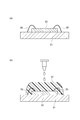
- a glass substrate is disposed above the microlens via an adhesive layer and a cavity.
- a wiring layer is disposed on the other surface of the semiconductor substrate. According to this back-illuminated structure, the light incident on the microlens is received by the light receiving unit without passing through the wiring layer, so that attenuation of light by the wiring layer is avoided and the light receiving sensitivity is increased.
- an adhesive layer disposed on the outer peripheral side so as not to cover the microlens is surrounded by the adhesive layer on a silicon substrate including the microlens.
- a structure in which a glass substrate is arranged through a low refractive index layer filled in a cavity see, for example, Patent Document 3 below.
- the adhesive composition when manufacturing a semiconductor device such as an optical component, various properties are required for the adhesive composition depending on a construction method or a package structure. For example, from the viewpoint of reducing optical loss, the cured product of the adhesive composition is required to have excellent transparency. In addition, in order to apply the adhesive composition at a high speed only in a limited narrow area, an excellent viscosity (thixotropic property) that can be applied to a dispensing method or the like is required.
- the present invention has been made in view of the above circumstances, and an object of the present invention is to provide an adhesive composition having excellent viscosity while being able to obtain a cured product having excellent transparency. Another object of the present invention is to provide a cured product having excellent transparency. Furthermore, an object of this invention is to provide the semiconductor device using the said adhesive composition, and its manufacturing method.
- the present invention contains (a) a (meth) acrylic polymer, (b) a compound having at least two (meth) acryloyl groups, (c) a polymerization initiator, and (d) a filler.
- An adhesive composition is provided.
- the adhesive composition according to the present invention a cured product having excellent transparency can be obtained.
- the adhesive composition according to the present invention has an excellent viscosity and has thixotropic properties suitable for the dispensing method and the like.
- the adhesive composition according to the present invention is excellent in reflow peel resistance (for example, 260 ° C.).
- the refractive index of the cured product can be arbitrarily adjusted within a suitable range.
- the content of the component (d) is preferably 0.1 to 40 parts by mass with respect to 100 parts by mass as a total of the components (a) and (b).
- the average particle size of the component (d) is preferably 5 to 10,000 nm.
- the component (a) preferably has an alicyclic structure.
- the amorphous component in a (meth) acryl polymer increases, it exists in the tendency for transparency to become still higher. Further, compared with an aliphatic structure having the same carbon number (such as an aliphatic structural unit), the glass transition temperature (Tg) is improved and the heat resistance tends to be increased.
- the component preferably has an epoxy group. Thereby, the adhesiveness to the board
- the component (a) may have a structural unit represented by the following general formula (I).
- R 1a represents a hydrogen atom or a methyl group
- X a represents a group containing an epoxy group.
- the adhesive composition according to the present invention can further contain an antioxidant. Thereby, the coloring by the deterioration at the time of heat
- the adhesive composition according to the present invention may be used for optical parts. Since the adhesive composition according to this embodiment is excellent in transparency and viscosity, it can be suitably used as a potting material.
- the adhesive composition according to the present invention tends to have a refractive index larger than that of air, has high transparency after curing, and is excellent in reflow peel resistance, and therefore is preferably used for optical parts. Is possible, and in that case, a particularly excellent effect is exhibited. Moreover, it can use suitably as a sealing member of a light emitting element (LED element etc.) or a light receiving element (CMOS element etc.).
- the present invention also provides a cured product of the above-described adhesive composition.
- the present invention provides a step of forming an adhesive layer containing the above-described adhesive composition on a semiconductor substrate, and the bonding in a state where the adhesive layer is disposed between the semiconductor substrate and a transparent substrate. And a step of curing the agent layer.
- the above-described adhesive composition has an excellent function as an adhesive, and has high transparency even after curing. Therefore, an excellent effect is exhibited by using the adhesive composition in the manufacturing process of a semiconductor device. In addition, the characteristics of the obtained semiconductor device are also improved.
- the present invention comprises a semiconductor substrate, an adhesive layer disposed on the semiconductor substrate, and a transparent base material bonded to the semiconductor substrate via the adhesive layer, wherein the adhesive layer is A semiconductor device comprising the above-described adhesive composition or a cured product thereof is provided.
- the above-described adhesive composition has an excellent function as an adhesive and has high transparency even after curing. Therefore, particularly excellent effects are exhibited by using the adhesive composition. Will also be good.
- a cured product having excellent transparency can be obtained, and an adhesive composition having excellent viscosity can be provided.
- cured material which has the outstanding transparency can be provided.
- the semiconductor device for example, optical components, such as a solid-state image sensor using the said adhesive composition, and its manufacturing method can be provided.
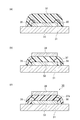
- the adhesive composition and the cured product thereof according to the present invention have an adhesive layer disposed on the outer peripheral side of the substrate so as not to cover the microlens, and are surrounded by a cavity (cavity) surrounded by the adhesive layer ) In which the adhesive composition or the cured product thereof is filled, and a configuration in which an adhesive layer formed of the adhesive composition is formed on the entire surface of the substrate.
- a semiconductor composition or a resin composition (adhesive composition) for manufacturing the semiconductor device can be provided.
- ADVANTAGE OF THE INVENTION use of the resin composition (adhesive composition) for an optical component or its manufacture can be provided.
- ADVANTAGE OF THE INVENTION use of the resin composition (adhesive composition) for a solid-state image sensor or its manufacture can be provided.
- ADVANTAGE OF THE INVENTION use of the hardened
- ADVANTAGE OF THE INVENTION use of the hardened
- ADVANTAGE OF THE INVENTION use of the hardened
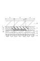
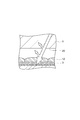
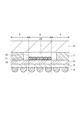
- FIG. 4 is a sectional view taken along line A-A ′ shown in FIG. 3. It is sectional drawing which shows the other example of a semiconductor device. It is sectional drawing which shows an example of a noncavity structure. It is sectional drawing which shows an example of a cavity structure. It is drawing for contrasting the manufacturing method of a semiconductor device. It is sectional drawing which shows an example of the conventional back irradiation type solid-state image sensor which has a cavity structure.
- (meth) acryloyl group means at least one of “acryloyl group” and “methacryloyl group” corresponding thereto. The same applies to other similar expressions such as “(meth) acrylate”.
- a high “transparency” means that the visible light transmittance in the cured product of the adhesive composition is good, and an interaction occurs between the adhesive composition and the visible light. It means that absorption and scattering of electromagnetic waves are difficult to occur.
- the lower limit of the wavelength of electromagnetic waves corresponding to visible light is approximately 400 nm, and the upper limit is approximately 760 nm.
- a transmittance representing the intensity ratio of incident light and transmitted light as a percentage can be used.
- “Refractive index” means a relative refractive index when the refractive index of air is 1.000.
- a numerical range indicated by using “to” indicates a range including the numerical values described before and after “to” as the minimum value and the maximum value, respectively.
- the upper limit value or lower limit value of a numerical range of a certain step may be replaced with the upper limit value or lower limit value of the numerical range of another step.
- the upper limit value or the lower limit value of the numerical range may be replaced with the values shown in the examples.
- the terms “layer” and “film” include not only a structure formed on the entire surface but also a structure formed on a part when observed as a plan view.
- process is not limited to an independent process, and is included in the term if the intended purpose of the process is achieved even if it cannot be clearly distinguished from other processes.
- a or B only needs to include either A or B, and may include both.
- the content of each component in the composition is the total amount of the plurality of substances present in the composition unless there is a specific notice when there are a plurality of substances corresponding to each component in the composition. Means.
- the adhesive composition according to this embodiment includes (a) a (meth) acrylic polymer (hereinafter sometimes referred to as “component (a)”) and (b) a compound having at least two (meth) acryloyl groups ( Hereinafter, sometimes referred to as “(b) component”), (c) polymerization initiator (hereinafter, sometimes referred to as “(c) component”), and (d) filler (hereinafter, sometimes referred to as “(d) component”). And).
- the cured product according to the present embodiment is a cured product of the adhesive composition according to the present embodiment.
- the adhesive composition according to this embodiment may be liquid (varnish-like) or film-like.
- the adhesive composition according to the present embodiment can be used as an adhesive composition for semiconductor devices, and for example, can be used as an adhesive composition for optical components.
- the thixotropic property suitable for the dispensing method or the like is obtained by using the filler as the component (d) together with the component (a), the component (b) and the component (c). Can be obtained.
- a (meth) acrylic polymer is a material that is expected to relieve stress because it has rubber elasticity, but the heat resistance of the (meth) acrylic polymer itself is low, and an adhesive for a semiconductor device obtained through a reflow process It is thought that it is unsuitable for.
- the adhesive composition according to the present embodiment the combined use of a (meth) acrylic polymer and a compound having at least two (meth) acryloyl groups can sufficiently suppress a decrease in heat resistance. it can. This is considered to be because heat resistance can be improved by forming a three-dimensional bridge with a compound having at least two (meth) acryloyl groups.
- the compatibility between the (meth) acrylic polymer and the compound having at least two (meth) acryloyl groups is high, and these refractive indexes tend to be close to each other. Excellent transparency that can ensure visibility after curing can be obtained. Furthermore, since the compatibility is high as described above, phase separation hardly occurs in a varnish state or a semi-cured state, and the storage stability is also excellent. Further, even when phase separation occurs due to the heat of curing after radical curing, only micro phase separation is achieved, and variations in cured properties such as visibility and adhesive strength can be suppressed. The problem of light loss can also be solved by filling the cavity with the adhesive composition according to this embodiment.
- the “(meth) acrylic polymer” is a polymer having a structural unit derived from a monomer having a (meth) acryloyl group ((meth) acrylic monomer).
- the monomer copolymerizable with the (meth) acrylic monomer a compound having two or more (meth) acryloyl groups in one molecule; one polymerizable unsaturated bond in one molecule, And a polymerizable compound having no (meth) acryloyl group (for example, (meth) acrylonitrile, styrene, vinyl acetate and alkene (ethylene, propylene, etc.)); two or more polymerizable unsaturated bonds in one molecule And a polymerizable compound (divinylbenzene, etc.) having a (meth) acryloyl group.
- a component can be used individually by 1 type or in combination of 2 or more types.
- the component (a) is derived from a (meth) acrylic monomer having one (meth) acryloyl group in one molecule based on the total amount of the component (a).
- the structural unit is preferably 30 to 100% by mass, and more preferably 50 to 100% by mass.
- the component (a) preferably has a functional group, for example, preferably has a structural unit having a functional group. In these cases, excellent stress relaxation, reflow peel resistance, crack resistance, adhesion and heat resistance associated with a low elastic modulus can be easily expressed.
- the functional group at least one selected from the group consisting of a carboxyl group, an acid anhydride group, a hydroxyl group, an amino group, an amide group, a phosphoric acid group, a cyano group, a maleimide group, and an epoxy group can be used.
- an epoxy group is preferable.
- the method for introducing the functional group into the (meth) acrylic polymer is not particularly limited.
- a functional group is introduced into the (meth) acrylic polymer by random polymerization of a functional group-containing monomer having a functional group, for example, as described in International Publication No. 2015/115537. be able to. Of these, suspension polymerization is preferable from the viewpoint of high molecular weight at low cost.
- Suspension polymerization is performed by adding a suspending agent in an aqueous solvent.
- a suspending agent it is preferable to use a nonionic water-soluble polymer from the viewpoint that ionic impurities are less likely to remain in the resulting (meth) acrylic polymer.
- the amount of the water-soluble polymer used is preferably 0.01 to 1 part by mass with respect to 100 parts by mass of the total amount of monomers.
- polymerization initiators In the polymerization reaction, commonly used polymerization initiators, chain transfer agents and the like may be used.
- the polymerization initiator include the same compounds as the (c) polymerization initiator described later.
- the chain transfer agent include thiols such as n-octyl mercaptan.
- the functional group-containing monomer is at least one selected from the group consisting of a carboxyl group, an acid anhydride group, a hydroxyl group, an amino group, an amide group, a phosphoric acid group, a cyano group, a maleimide group, and an epoxy group in one molecule. And at least one polymerizable carbon-carbon double bond.
- the functional group is an amino group, an amide group, a phosphate group, a cyano group, from the viewpoint of easily avoiding problems such as gelation in a varnish state, nozzles during use, that is, pinhole generation during spin coating, and the like. It is preferably at least one selected from the group consisting of a maleimide group and an epoxy group. In addition, the functional group is preferably at least one selected from the group consisting of a carboxyl group, an acid anhydride group, a hydroxyl group, a phosphoric acid group, and an epoxy group from the viewpoint of preventing coloring more highly. Furthermore, from both these viewpoints, the functional group is preferably at least one selected from the group consisting of a phosphate group and an epoxy group, and more preferably an epoxy group.
- Examples of the functional group-containing monomer include a carboxyl group-containing monomer, an acid anhydride group-containing monomer, a hydroxyl group-containing monomer, and an amino group-containing monomer as exemplified in International Publication No. 2015/115537.
- Phosphoric acid group-containing monomers vinyl cyanide compounds; N-substituted maleimides; epoxy group-containing monomers, and the like.
- a functional group containing monomer can be used individually by 1 type or in combination of 2 or more types.
- an epoxy group-containing monomer such as glycidyl (meth) acrylate.
- the (meth) acrylic polymer obtained by using such a monomer is compatible with the (meth) acrylic monomer or oligomer.
- the glycidyl group-containing (meth) acrylic polymer may be synthesized by a conventional method, or a commercially available product may be obtained. Examples of commercially available products include HTR-860P-3 (Nagase ChemteX Corporation, trade name).
- Such a (meth) acrylic polymer is preferable from the viewpoint of further exhibiting excellent crack resistance, adhesion, and heat resistance, and from the viewpoint of easily ensuring excellent storage stability.
- the content of the structural unit having the functional group is preferably in the following range based on the total amount of the component (a) from the viewpoint of easily securing adhesive force and easily preventing gelation.
- the content of the structural unit having a functional group is preferably 0.5% by mass or more, more preferably 0.8% by mass or more, further preferably 1.0% by mass or more, and particularly preferably 2.0% by mass or more. 3.0% by mass or more is extremely preferable.
- the content of the structural unit having a functional group is preferably 20% by mass or less, more preferably 10% by mass or less, still more preferably 6.0% by mass or less, and particularly preferably 5.0% by mass or less.
- the content of the structural unit having a functional group is preferably 0.5 to 20% by mass, more preferably 0.5 to 10% by mass, and further preferably 0.5 to 6.0% by mass.
- 0.5 to 5.0% by weight is particularly preferable, 0.8 to 5.0% by weight is very preferable, 1.0 to 5.0% by weight is very preferable, and 2.0 to 5.0% by weight. Is more preferable, and 3.0 to 5.0% by mass is even more preferable.
- the component may have a structural unit having a nitrogen atom-containing group.
- the content of the structural unit having a nitrogen atom-containing group in the component (a) is preferably 5% by mass or less, more preferably 3% by mass or less, still more preferably 1% by mass or less, based on the total amount of the component (a). . It is particularly preferable that the component (a) does not contain a structural unit having a nitrogen atom-containing group.
- the nitrogen atom-containing group include an amino group, an amide group, a cyano group, and a maleimide group.
- Examples of the structural unit having a nitrogen atom-containing group include structural units derived from monomers containing a nitrogen atom among the functional group-containing monomers listed above, and cyanation of (meth) acrylonitrile and the like. Examples include structural units derived from vinyl compounds.
- Examples of monomers other than the functional group-containing monomer that can be used in the synthesis of the component (a) include (meth) acrylic acid esters as exemplified in International Publication No. 2015/115537; Group vinyl compounds; alicyclic monomers and the like. Monomers other than the functional group-containing monomer can be used singly or in combination of two or more.
- (meth) acrylic acid esters are preferable from the viewpoint of easily synthesizing a (meth) acrylic polymer (for example, a (meth) acrylic polymer having a weight average molecular weight of 100,000 or more) without gelation.
- a (meth) acrylic acid esters from the viewpoint of excellent copolymerizability with a functional group-containing monomer, ethyl (meth) acrylate, butyl (meth) acrylate, and 2-ethylhexyl (meth) acrylate More preferred is at least one selected from the group consisting of
- the component (a) preferably has at least one selected from the group consisting of an alicyclic structure and a heterocyclic structure, and more preferably has an alicyclic structure.
- the component (a) preferably has a structural unit having at least one selected from the group consisting of an alicyclic structure and a heterocyclic structure, and more preferably has a structural unit having an alicyclic structure.
- Examples of the monomer having an alicyclic structure or a heterocyclic structure used in producing a (meth) acrylic polymer having a structural unit having an alicyclic structure or a heterocyclic structure include, for example, the following general The compound represented by Formula (1) is mentioned.
- R 1 represents a hydrogen atom or a methyl group
- R 2 represents an alicyclic group or a heterocyclic group
- X represents an alkylene group having 1 to 6 carbon atoms
- n represents 0 to 10 Indicates an integer.
- n is an integer of 2 or more, a plurality of Xs may be the same or different from each other.
- the “alicyclic group” is a group having a structure in which carbon atoms are bonded cyclically
- the “heterocyclic group” is a group having a structure in which a carbon atom and one or more heteroatoms are bonded cyclically. is there.
- R 2 examples include groups represented by the following formulas (2a) to (2h).
- R 3 , R 4 , R 5 , R 6 , R 7 , R 8 , R 9 and R 10 each independently represents a hydrogen atom or an alkyl group having 1 to 4 carbon atoms
- R 11 represents hydrogen An atom, an alkyl group having 1 to 4 carbon atoms, or a structure represented by OR 11a is shown, and R 11a represents a hydrogen atom or an alkyl group having 1 to 8 carbon atoms.
- Examples of the compound represented by the formula (1) include cyclohexyl (meth) acrylate (also known as cyclohexyl (meth) acrylate), isobornyl (meth) acrylate (also known as isobornyl (meth) acrylate), and (meth) ) Acrylic acid tricyclo [5.2.1.0 2,6 ] dec-8-yl (also known as: tricyclo [5.2.1.0 2,6 ] decyl (meth) acrylate).
- the content of these monomers other than the functional group-containing monomer is not particularly limited, but is preferably adjusted so that the Tg of the component (a) is in the range of ⁇ 50 to 50 ° C.
- the Tg of the component (a) is in the range of ⁇ 50 to 50 ° C.
- 2.5% by mass of glycidyl methacrylate, 43.5% by mass of methyl methacrylate, 18.5% by mass of ethyl acrylate, and 35.5% by mass of butyl acrylate are used as monomers.
- the component (a) which is an epoxy group-containing (meth) acrylic polymer having a Tg of 12 ° C. and a weight average molecular weight of 100,000 or more can be synthesized.
- the mixing ratio is determined in consideration of the Tg of the (meth) acrylic polymer, and the Tg of the component (a) is preferably ⁇ 50 ° C. or higher. This is because when the Tg is ⁇ 50 ° C. or higher, the tackiness of the adhesive composition in the B-stage state is appropriate, and the handleability is excellent.
- the mixing ratio of the functional group-containing monomer and the monomer other than the functional group-containing monomer is 100: 0 to 0.1: 99.9, preferably 100: 0 to 1:99, more preferably 50:50 to 1:99, 30:70 to A ratio of 1:99 is particularly preferred, and a ratio of 20:80 to 1:99 is very particularly preferred.
- the component (a) is composed of a structural unit represented by the following general formula (I), a structural unit represented by the following general formula (II), and a structural unit represented by the following general formula (III). You may have at least 1 sort chosen.
- R 1a represents a hydrogen atom or a methyl group
- X a represents a group containing an epoxy group
- R 2a represents a hydrogen atom or a methyl group
- Y a represents an alicyclic group having 5 to 22 carbon atoms which may have a substituent (corresponding to X in the formula (I) The group to be excluded).
- R 3a represents a hydrogen atom or a methyl group
- Z a represents a linear or branched alkyl group having 1 to 10 carbon atoms which may have a substituent
- Formula (I) The group corresponding to X is excluded).
- the polymerization method is not particularly limited, and solution polymerization, The above-mentioned methods such as suspension polymerization (pearl polymerization) can be used.
- the weight average molecular weight of the component (a) is appropriate in terms of strength, flexibility and tackiness after film formation, and appropriate flowability. The range of is preferable.
- the weight average molecular weight of the component (a) is preferably 100,000 or more, more preferably 120,000 or more, and further preferably 200,000 or more, from the viewpoint of maintaining a sufficient elastic modulus (for example, an elastic modulus of 260 ° C.). 300,000 or more is particularly preferable, 400,000 or more is extremely preferable, and 450,000 or more is very preferable.
- the weight average molecular weight of the component (a) is preferably 3 million or less, more preferably 2 million or less, still more preferably 1 million or less, and particularly preferably 800,000 or less.
- the weight average molecular weight of the component (a) is preferably 100,000 or more, more preferably 120,000 to 3,000,000, further preferably 120,000 to 2,000,000, particularly preferably 200,000 to 1,000,000, and 300,000. ⁇ 1 million is very preferable, 400,000 to 800,000 is even more preferable, and 450,000 to 800,000 is still more preferable.
- the weight average molecular weight is a value measured by gel permeation chromatography (GPC) and converted using a standard polystyrene calibration curve as described in Examples.
- the content of the component (a) shows a good storage elastic modulus, can suppress the flow at the time of molding, and from the viewpoint that the handleability at high temperature is sufficiently obtained, the total amount of the component (b) is 100 parts by mass. On the other hand, the following ranges are preferable.
- the content of the component (a) is preferably 10 parts by mass or more, more preferably 15 parts by mass or more, further preferably 20 parts by mass or more, particularly preferably 50 parts by mass or more, particularly preferably 75 parts by mass or more, and 100 parts by mass. Part or more is highly preferred.
- the content of the component (a) is preferably 10 to 400 parts by mass, more preferably 15 to 350 parts by mass, further preferably 20 to 300 parts by mass, particularly preferably 50 to 200 parts by mass, and 75 ⁇ 150 parts by mass is very preferable, and 100 to 150 parts by mass is very preferable.
- ((B) Compound having at least two (meth) acryloyl groups examples include (meth) acrylic monomers and oligomers thereof (excluding compounds corresponding to the component (a)).
- the molecular weight (for example, weight average molecular weight) of the component (b) may be, for example, 20,000 or less or 10,000 or less.
- the monomer having at least two (meth) acryloyl groups is not particularly limited, and a polyfunctional (meth) acrylic monomer having an alicyclic structure, a polyfunctional (meth) acrylic monomer having an aliphatic structure.
- Body a polyfunctional (meth) acrylic monomer having a dioxane glycol structure, a polyfunctional (meth) acrylic monomer having a functional group (excluding a (meth) acryloyl group), and the like.
- the polyfunctional (meth) acrylic monomer having a functional group a polyfunctional (meth) acrylic monomer having an alicyclic structure, an aliphatic structure or a dioxane glycol structure is excluded.
- polyfunctional refers to a (meth) acryloyl group, and means that the compound has at least two (meth) acryloyl groups.
- a component can be used individually by 1 type or in combination of 2 or more types.
- Component (b) is a polyfunctional (meth) acrylic monomer having an alicyclic structure and a polyfunctional (meth) acrylic monomer having a dioxane glycol structure from the viewpoint of further improving the transparency of the cured product. At least one selected from the group consisting of The component (b) is preferably a polyfunctional (meth) acrylic monomer having an aliphatic structure from the viewpoint of easily preventing cracks in the cured product and peeling from the substrate.
- polyfunctional (meth) acrylic monomers include (meth) acrylic monomers having two (meth) acryloyl groups.
- Examples of the (meth) acrylic monomer having two (meth) acryloyl groups include cyclohexane-1,4-dimethanol di (meth) acrylate, cyclohexane-1,3-dimethanol di (meth) acrylate, tricyclodecane dimethylol di ( (Meth) acrylate (for example, Nippon Kayaku Co., Ltd., KAYARAD R-684, tricyclodecane dimethylol diacrylate), tricyclodecane dimethanol di (meth) acrylate (for example, Shin-Nakamura Chemical Co., Ltd., A-DCP, Tricyclodecane dimethanol diacrylate), dioxane glycol di (meth) acrylate (for example, Shin-Nakamura Chemical Co., Ltd., A-DOG, dioxane glycol diacrylate), nonanediol di (meth) acrylate, neopentylglycol Di (meth)
- At least one selected from the group consisting of dioxane glycol di (meth) acrylate and tricyclodecane dimethanol di (meth) acrylate is preferable, and dioxane glycol diacrylate. And at least one selected from the group consisting of tricyclodecane dimethanol diacrylate is more preferable.
- Examples of other polyfunctional (meth) acrylic monomers include three (meth) acryloyl groups such as pentaerythritol tri (meth) acrylate and ethylene oxide-modified isocyanuric acid tri (meth) acrylate (meth). An acrylic monomer can be mentioned.
- the content of the component (b) is preferably 20 parts by mass or more, more preferably 30 parts by mass or more, and still more preferably 40 parts by mass or more with respect to 100 parts by mass of the total amount of the components (a) and (b).
- the content of the component (b) is preferably 80 parts by mass or less, more preferably 70 parts by mass or less, still more preferably 60 parts by mass or less, with respect to 100 parts by mass of the total amount of the components (a) and (b). 50 parts by mass or less is particularly preferable.
- the content of the component (b) is preferably 20 to 80 parts by weight, more preferably 30 to 70 parts by weight, and more preferably 40 to 60 parts by weight with respect to 100 parts by weight as the total of the components (a) and (b).
- the content of the component (b) is within the above ranges, three-dimensional crosslinking is easily performed, and thus heat resistance tends to be further improved. Even if phase separation occurs after curing, the phase separation range can be kept on a microscale. Therefore, variations in cured product characteristics such as visibility and adhesive strength can be easily suppressed, and warpage or cracks in the manufacturing process of a semiconductor or electronic component can be easily suppressed.
- (c) polymerization initiator examples include (c1) a thermal polymerization initiator (hereinafter, sometimes referred to as “(c1) component”) and / or (c2) a photopolymerization initiator (hereinafter, sometimes referred to as “(c2)”. Component)).
- (C1) examples of the component include organic peroxides; azo compounds as exemplified in International Publication No. 2015/115537.
- (C1) A component can be used individually by 1 type or in combination of 2 or more types.
- an organic peroxide is preferable from the viewpoint of a large effect of improving the properties of the cured product, and a good balance between the handleability of the adhesive composition (shelf life, pot life, etc.) and curability. From the viewpoint of maintaining, an organic peroxide having a 10-hour half-life temperature of 90 to 150 ° C. is more preferable. The half-life temperature of the organic peroxide can be measured by the method described in International Publication No. 2015/115537.
- dicumyl peroxide for example, trade name: Park Mill D, manufactured by NOF Corporation
- n-butyl 4,4-bis (t-butylperoxy) valerate for example, NOF Corporation, trade name: Perhexa V
- the component (c1) improves the reliability of semiconductor devices (optical components, etc.) by exhibiting superior heat resistance, peel resistance and stress relaxation in combination with the components (a) and (b). Can be made.
- the content of the component (c1) is in the following range with respect to 100 parts by mass of the total amount of the component (a) and the component (b), from the viewpoint of further improving the transparency and the viewpoint of easily suppressing the generation of outgas. Is preferred.
- the content of the component (c1) is preferably 0.1 parts by mass or more, more preferably 0.2 parts by mass or more, further preferably 0.5 parts by mass or more, and particularly preferably 1 part by mass or more.
- the content of the component (c1) is preferably 30 parts by mass or less, more preferably 20 parts by mass or less, further preferably 10 parts by mass or less, particularly preferably 5 parts by mass or less, and extremely preferably 3 parts by mass or less.
- the content of the component (c1) is preferably 0.1 to 30 parts by mass, more preferably 0.2 to 20 parts by mass, still more preferably 0.5 to 10 parts by mass, and particularly preferably 0.5 to 5 parts by mass. It is preferably 1 to 3 parts by mass.
- component (c2) acylphosphine oxides, oxime esters, aromatic ketones, quinones, benzoin ether compounds, benzyl derivatives, 2,4,5-triarylimidazole dimers, acridine derivatives, coumarin compounds, N-phenylglycine, N-phenylglycine derivatives and the like can be mentioned.
- C2 A component may be synthesize
- acylphosphine oxides and oxime esters from the viewpoints of improving photocurability, improving sensitivity, and further improving the transparency of cured products (cured films, etc.). At least one is preferred.
- a component can be used individually by 1 type or in combination of 2 or more types.
- acylphosphine oxide examples include bis (2,4,6-trimethylbenzoyl) -phenylphosphine oxide (for example, IRGACURE-819, trade name of BASF), 2,4,6-trimethylbenzoyl-diphenylphosphine oxide. (For example, LUCIRIN TPO, BASF, trade name) and the like.
- oxime esters examples include 1,2-octanedione-1- [4- (phenylthio) phenyl-2- (O-benzoyloxime)] (for example, IRGACURE-OXE01, trade name of BASF Corporation), 1- [9 -Ethyl-6- (2-methylbenzoyl) -9H-carbazol-3-yl] ethanone-1- (O-acetyloxime) (for example, IRGACURE-OXE02, BASF, trade name), 1-phenyl-1, 2-propanedione-2- [o- (ethoxycarbonyl) oxime] (for example, Quantacure-PDO, Nippon Kayaku Co., Ltd., trade name) and the like.
- IRGACURE-OXE01 trade name of BASF Corporation
- aromatic ketones examples include compounds described in International Publication No. 2015/115537.
- quinones examples include compounds described in International Publication No. 2015/115537.
- benzoin ether compound examples include benzoin methyl ether, benzoin ethyl ether, and benzoin phenyl ether.
- benzyl derivative examples include benzoin compounds such as benzoin, methylbenzoin, and ethylbenzoin; benzyldimethyl ketal and the like.
- 2,4,5-triarylimidazole dimer examples include compounds described in International Publication No. 2015/115537.
- acridine derivative examples include 9-phenylacridine, 1,7-bis (9,9'-acridinyl) heptane and the like.
- Examples of the coumarin compound include compounds described in International Publication No. 2015/115537.
- N-phenylglycine derivatives include N-phenylglycine butyl ester, Np-methylphenylglycine, Np-methylphenylglycine methyl ester, N- (2,4-dimethylphenyl) glycine, N-methoxyphenylglycine Etc.
- the content of the component (c2) is preferably 0.1 to 20 parts by mass, more preferably 0.5 to 10 parts by mass with respect to 100 parts by mass of the total amount of the components (a) and (b). More preferred is 75-5 parts by mass.
- content of the component (c2) is within these ranges, foaming, turbidity, coloring and cracking of the cured product can be further prevented.
- (D) filler) As a filler which is a component, an inorganic filler, an organic filler, etc. are mentioned. As the component (d), an inorganic filler is preferable from the viewpoint of further improving the heat resistance or thermal conductivity, the viewpoint of suitably adjusting the melt viscosity, or the viewpoint of further suitably imparting thixotropic properties.
- a component can be used individually by 1 type or in combination of 2 or more types.
- the inorganic filler content is not particularly limited, and includes aluminum hydroxide, magnesium hydroxide, calcium carbonate, magnesium carbonate, calcium silicate, magnesium silicate, calcium oxide, magnesium oxide, aluminum oxide, aluminum nitride, titanium oxide, Examples thereof include zirconium oxide, cerium oxide, zinc oxide, aluminum borate whisker, boron nitride, silica (crystalline silica, amorphous silica, etc.), antimony oxide, metal (silver, etc.), and the like.
- a glass filler can be used as the component (d).
- the glass filler contains silica (SiO 2 ) and may contain ZrO 2 , B 2 O 3 , Na 2 O, F 2 , Al 2 O 3 , CaO, MgO, SrO and the like at a certain ratio.
- the inorganic filler component is at least one selected from the group consisting of aluminum oxide, aluminum nitride, boron nitride and silica (silicon oxide, crystalline silica, amorphous silica, etc.) from the viewpoint of further improving thermal conductivity. Species are preferred.
- silica silicon oxide, crystalline silica, amorphous silica, etc.
- aluminum hydroxide, magnesium hydroxide, calcium carbonate, magnesium carbonate, calcium silicate, magnesium silicate, calcium oxide At least one selected from the group consisting of magnesium oxide, aluminum oxide and silica (crystalline silica, amorphous silica, etc.) is preferred.
- the component containing the inorganic filler is preferably at least one selected from the group consisting of zirconium oxide, titanium oxide, silver and glass from the viewpoint of easy adjustment of the refractive index.
- silica is preferable and amorphous silica is more preferable from the viewpoint of obtaining further excellent transparency, refractive index, and workability.
- the refractive index of the component (d) is preferably 1.46 to 1.60, more preferably 1.48 to 1.54, from the viewpoint of further improving the transparency when the components (a) and (b) are combined.
- the preferred range is 1.49 to 1.52.
- the average particle size of the component (d) is preferably 5 nm or more, more preferably 10 nm or more, still more preferably 12 nm or more, and further preferably 15 nm from the viewpoint of excellent dispersibility and workability and further excellent thixotropic properties. The above is particularly preferable.
- the average particle diameter of the component (d) is preferably 10,000 nm or less, more preferably 5000 nm or less, and more preferably 1000 nm from the viewpoint of further excellent transparency and excellent workability in filtration of the resin composition (adhesive composition).
- the average particle size of the component (d) is preferably from 5 to 10,000 nm, more preferably from 10 to 5000 nm, still more preferably from 10 to 1000 nm, from the viewpoint of more suitably imparting thixotropic properties while maintaining transparency.
- 500 nm is particularly preferable, 12 to 300 nm is very preferable, 15 to 100 nm is very preferable, and 15 to 50 nm is even more preferable.
- the average particle diameter of a component is an average particle diameter of the filler in the state disperse
- a solvent such as methyl ethyl ketone
- the particle diameter at the integrated value 99.9% (volume basis) in the particle size distribution is defined as the maximum particle diameter.
- the adhesive resin layer (uncured) arrange
- the content of the component (d) is preferably in the following range with respect to 100 parts by mass of the total amount of the component (a) and the component (b) from the viewpoint of obtaining further excellent transparency, refractive index and workability.
- the content of the component (d) is preferably 0.1 parts by mass or more, more preferably 0.2 parts by mass or more, further preferably 0.3 parts by mass or more, particularly preferably 0.5 parts by mass or more, and 1 part by mass. Is more preferably 2 parts by mass or more, still more preferably 5 parts by mass or more, still more preferably 7.5 parts by mass or more, and particularly preferably 10 parts by mass or more.
- component (D) As for content of a component, 40 mass parts or less are preferable, 30 mass parts or less are more preferable, and 20 mass parts or less are still more preferable. From these viewpoints, the content of component (d) is preferably 0.1 to 40 parts by weight, more preferably 0.2 to 30 parts by weight, still more preferably 0.3 to 20 parts by weight, 20 parts by weight are particularly preferable, 1 to 20 parts by weight are very preferable, 2 to 20 parts by weight are very preferable, 5 to 20 parts by weight are even more preferable, 7.5 to 20 parts by weight are still more preferable, and Part by mass is particularly preferred.
- the content of SiO 2 in the component (d) is preferably 50 to 100% by mass on the basis of the entire component (d) from the viewpoint of further improving the transparency.
- SiO 2 content means the content of SiO 2 in the total amount of filler components.
- the adhesive composition according to the present embodiment can contain an antioxidant as necessary.
- the antioxidant include phenolic antioxidants, thioether antioxidants, and thiol antioxidants.
- Antioxidant can be used individually by 1 type or in combination of 2 or more types.
- phenolic antioxidants include hindered phenolic compounds.
- hindered phenol compound examples include compounds described in International Publication No. 2015/046422. Specifically, bis [3- (3-tert-butyl-4-hydroxy-5-methylphenyl) is exemplified. ) Propionic acid] (2,4,8,10-tetraoxaspiro [5.5] undecane-3,9-diyl) bis (2,2-dimethyl-2,1-ethanediyl).
- Examples of the thioether-based antioxidant include ditridecyl 3,3-thiobispropionate (for example, “ADEKA STAB AO-503” (ADEKA)).
- Examples of the thiol-based antioxidant include compounds having a thiol group.
- Examples of the compound having a thiol group include 1,3,5-tris (3-mercaptobutyryloxyethyl) -1,3,5-triazine-2,4,6 (1H, 3H, 5H) -trione (for example, "Karenz MT-NR1" (Kyoeisha Chemical Co., Ltd.)).
- the content of the antioxidant is 100 parts by mass of the total amount of the component (a), the component (b) and the component (c) from the viewpoint of further improving the transmittance and from the viewpoint of hardly adversely affecting the radical polymerization reactivity.
- the content of the antioxidant is preferably 0.01 parts by mass or more, more preferably 0.1 parts by mass or more, further preferably 1 part by mass or more, and particularly preferably 2 parts by mass or more. 10 mass parts or less are preferable, as for content of antioxidant, 8 mass parts or less are more preferable, 5 mass parts or less are still more preferable, and 4 mass parts or less are especially preferable. From these viewpoints, the content of the antioxidant is preferably 0.01 to 10 parts by mass, more preferably 0.1 to 8 parts by mass, still more preferably 1 to 5 parts by mass, and particularly preferably 2 to 4 parts by mass. preferable.
- the adhesive composition according to the present embodiment can contain a coupling agent.
- the coupling agent is not particularly limited, and various coupling agents such as a silane coupling agent, a titanate coupling agent, an aluminum coupling agent, a zirconate coupling agent, and a zircoaluminate coupling agent are used. be able to.
- a coupling agent can be used individually by 1 type or in combination of 2 or more types.
- the silane coupling agent may be an alkoxysilane.
- the silane coupling agent is, for example, at least one selected from the group consisting of a vinyl group, an epoxy group, a styryl group, a (meth) acryl group, an amino group, an isocyanurate group, a ureido group, a mercapto group, and an isocyanate group. It may be an alkoxysilane having a functional group.
- Specific examples of the silane coupling agent include compounds exemplified in International Publication No. 2015/115537.
- titanate coupling agents examples include compounds exemplified in International Publication No. 2015/115537.
- Examples of the aluminum coupling agent include acetoalkoxyaluminum diisopropionate.
- zirconate coupling agent examples include tetrapropyl zirconate, tetrabutyl zirconate, tetra (triethanolamine) zirconate, tetraisopropyl zirconate, zirconium acetylacetonate acetylacetone zirconium butyrate, and zirconium stearate butyrate.
- R 12 represents a carboxyl group or an amino group.
- Examples of the compound in which R 12 is a carboxyl group include Mansheim CPG-carboxyzircoaluminate.
- Examples of the compound in which R 12 is an amino group include Mansheim APO-X-amino zircoaluminate solution. Each is available from Rhône Poulenc.
- a silane coupling agent is preferable, a silane coupling agent having a (meth) acryl group is more preferable, and ⁇ - At least one selected from the group consisting of methacryloxypropyltrimethoxysilane (also known as 3- (trimethoxysilyl) propyl methacrylate), ⁇ -methacryloxypropylmethyldimethoxysilane, and ⁇ -acryloxypropyltrimethoxysilane; Further preferred.
- the content of the coupling agent is preferably in the following range with respect to 100 parts by mass of the total amount of the components (a), (b) and (c).
- the content of the coupling agent is preferably 0.1 parts by mass or more, more preferably 0.5 parts by mass or more, and even more preferably 0.8 parts by mass or more from the viewpoint that the effect of improving the adhesive strength tends to be obtained.
- the content of the coupling agent is preferably 20 parts by mass or less, more preferably 15 parts by mass or less, and more preferably 10 parts by mass from the viewpoint that the volatile content is small and generation of voids in the cured product tends to be easily suppressed.
- the content of the coupling agent is preferably 0.1 to 20 parts by mass, more preferably 0.5 to 15 parts by mass, still more preferably 0.8 to 10 parts by mass, and 0.8 to 5 parts by mass.
- Part by mass is particularly preferred, 0.8 to 3 parts by mass is very particularly preferred and 0.8 to 1 part by mass is very particularly preferred.
- the adhesive composition according to this embodiment may contain an epoxy curing agent.
- the epoxy curing agent can be used together with a compound having an epoxy group.
- curing agent What is necessary is just a compound which can react with the compound which has an epoxy group.
- the molecular weight of the epoxy curing agent is preferably about 100 to 400.
- the epoxy curing agent is preferably colorless or relatively uncolored (for example, light yellow). Examples of the epoxy curing agent include an acid anhydride curing agent, an isocyanuric acid derivative, and a phenol curing agent.
- curing agent can be used individually by 1 type or in combination of 2 or more types.
- acid anhydride curing agents include phthalic anhydride, maleic anhydride, trimellitic anhydride, pyromellitic anhydride, hexahydrophthalic anhydride, tetrahydrophthalic anhydride, methyl nadic anhydride, nadic anhydride, glutaric anhydride, Examples thereof include dimethyl glutaric anhydride, diethyl glutaric anhydride, succinic anhydride, methyl hexahydrophthalic anhydride, methyl tetrahydrophthalic anhydride, and derivatives thereof.
- acid anhydride curing agents examples include 3or4-methyl-1,2,3,6-tetrahydrophthalic anhydride, 3or4-methyl-hexahydrophthalic anhydride, methyl-3,6 endomethylene- Examples include 1,2,3,6-tetrahydrophthalic anhydride.
- Isocyanuric acid derivatives include 1,3,5-tris (1-carboxymethyl) isocyanurate, 1,3,5-tris (2-carboxyethyl) isocyanurate, 1,3,5-tris (3-carboxypropyl) ) Isocyanurate, 1,3-bis (2-carboxyethyl) isocyanurate and the like.
- a novolak type phenol resin obtained by condensation or cocondensation of phenols and / or naphthols and a compound having an aldehyde group (formaldehyde, benzaldehyde, salicylaldehyde, etc.) under an acidic catalyst; phenol And / or naphthols and phenol / aralkyl resins synthesized from dimethoxyparaxylene or bis (methoxymethyl) biphenyl; aralkyl type phenol resins such as biphenylene type phenol / aralkyl resins and naphthol / aralkyl resins; phenols and / or Or dicyclopentadiene type phenol resin synthesized by copolymerization of naphthols and dicyclopentadiene (dicyclopentadiene type phenol novolac resin, dicyclopentadiene type) Futol novolac resin, etc.
- phenols include phenol, cresol, resorcin, catechol, bisphenol A, bisphenol F, phenylphenol, and aminophenol.
- naphthols include ⁇ -naphthol, ⁇ -naphthol, dihydroxynaphthalene and the like.
- epoxy curing agents since it is a liquid curing agent, it is easy to mix with a compound having an epoxy group, has low toxicity compared to amine curing agents, and has a long pot life and stability. From the viewpoint of easily obtaining a cured product which is colorless and transparent and excellent in weather resistance and heat resistance, a phthalic anhydride-based epoxy curing agent (for example, 3or4-methyl-hexahydrophthalic anhydride (trade name: HN-5500 ( Hitachi Chemical Co., Ltd.) is preferred.
- a phthalic anhydride-based epoxy curing agent for example, 3or4-methyl-hexahydrophthalic anhydride (trade name: HN-5500 ( Hitachi Chemical Co., Ltd.) is preferred.
- the active group (an acid anhydride group) in the epoxy curing agent capable of reacting with the epoxy group is equivalent to 1 equivalent of the epoxy group in the compound having an epoxy group.
- Hydroxyl group, etc. is preferably 0.4 to 1.6 equivalents, more preferably 0.5 to 1.5 equivalents.
- the ratio of the active groups is 0.4 equivalent or more, the curing rate of the adhesive composition is sufficiently high, and the glass transition temperature of the obtained cured product is sufficiently high, so that a sufficient elastic modulus can be obtained.
- the ratio of the active group is 1.6 equivalents or less, the strength after curing is sufficiently high.
- Epoxy curing accelerator The adhesive composition according to the present embodiment may contain an epoxy curing accelerator as necessary.
- Epoxy curing accelerators include tertiary amines such as 1,8-diaza-bicyclo (5,4,0) undecene-7, triethylenediamine, tri-2,4,6-dimethylaminomethylphenol; 2-ethyl Imidazoles such as -4 methylimidazole and 2-methylimidazole; triphenylphosphine, tetraphenylphosphonium tetraphenylborate, tetra-n-butylphosphonium-o, o-diethylphosphorodithioate, tetra-n-butylphosphonium-tetra Phosphorus compounds such as fluoroborate, tetra-n-butylphosphonium-tetraphenylborate, and methyltributylphosphonium dimethyl phosphate; quaternary ammonium salts; organometallic salts
- the content of the epoxy curing accelerator is preferably in the following range based on the whole epoxy curing agent.
- the content of the epoxy curing accelerator is preferably 0.01% by mass or more, more preferably 0.1% by mass or more, and still more preferably 1.0% by mass or more from the viewpoint that a sufficient curing acceleration effect can be easily obtained.
- the content of the epoxy curing accelerator is preferably 8.0% by mass or less, more preferably 3.0% by mass or less, and more preferably 2.0% by mass or less from the viewpoint of easily suppressing discoloration of the obtained cured product. Further preferred. From these viewpoints, the content of the epoxy curing accelerator is preferably 0.01 to 8.0% by mass, more preferably 0.1 to 3.0% by mass, and further 1.0 to 2.0% by mass. preferable.
- the adhesive composition according to the present embodiment can contain an organic solvent as necessary. Thereby, a varnish-like adhesive composition can be obtained by melt
- the varnish-like adhesive composition has improved workability and improved workability on the substrate.
- the organic solvent is not particularly limited as long as it can uniformly stir, mix, dissolve, knead, or disperse the components contained in the adhesive composition, and a conventionally known solvent can be used.
- the organic solvent is not particularly limited, and examples thereof include alcohol solvents, ether solvents, ketone solvents, amide solvents, aromatic hydrocarbon solvents, ester solvents, and nitrile solvents. Specific examples include low boiling point solvents (diethyl ether, acetone, methanol, tetrahydrofuran, hexane, ethyl acetate, ethanol, methyl ethyl ketone, 2-propanol, etc.) from the viewpoint of easily suppressing volatilization at low temperatures.
- a high boiling point solvent toluene, methyl isobutyl ketone, 1-butanol, 2-methoxyethanol, 2-ethoxyethanol, xylene, N, N-dimethylacetamide, N, N-dimethylformamide Cyclohexanone, dimethylacetamide, butyl cellosolve, dimethyl sulfoxide, propylene glycol monomethyl ether acetate, N-methyl-2-pyrrolidone, ⁇ -butyrolactone, etc.).
- An organic solvent can be used individually by 1 type or in combination of 2 or more types.
- At least one selected from the group consisting of methyl ethyl ketone, cyclohexanone and propylene glycol monomethyl ether acetate is preferable from the viewpoint of excellent solubility and fast drying speed.
- the content of the organic solvent is determined by the viscosity when it is in a varnish state.
- the content of the organic solvent is not particularly limited, but is preferably 5 to 95% by mass, more preferably 10 to 90% by mass based on the entire adhesive composition.
- the adhesive composition according to this embodiment may contain a monofunctional (meth) acrylic monomer (a compound having one (meth) acryloyl group) separately from the component (b).
- a monofunctional (meth) acrylic monomer include the (meth) acrylic monomer exemplified by the component (a) (such as glycidyl (meth) acrylate).
- a monofunctional (meth) acryl monomer can be used individually by 1 type or in combination of 2 or more types.
- the adhesive composition according to the present embodiment includes, as necessary, a fluorosurfactant, a nonionic surfactant, a wetness improving agent such as a higher fatty acid; an antifoaming agent such as silicone oil; an inorganic ion exchanger, and the like.
- a fluorosurfactant such as a fluorosurfactant, a nonionic surfactant, a wetness improving agent such as a higher fatty acid; an antifoaming agent such as silicone oil; an inorganic ion exchanger, and the like.
- An ion trapping agent; a refractive index adjusting agent or a light absorber (UV absorber, IR absorber, etc.) can be contained. These can be used alone or in combination of two or more.
- the thixotropic property (also referred to as “thixotropic index”) of the adhesive composition according to the present embodiment is less likely to cause stringing and from the viewpoint of improving handling properties by facilitating liquid discharge. 1.3 or more is preferable, and 1.4 or more is more preferable.
- the upper limit of thixotropic property is preferably 5.0 or less, and more preferably 4.0 or less.
- the viscosity (TI) of the adhesive composition according to the present embodiment is measured by, for example, measuring the viscosity at low speed rotation (25 ° C.) and the viscosity at high speed rotation (25 ° C.) under the following conditions. Is calculated by T. T. et al.
- V2 / V1 V1 Viscosity at high speed (P)
- V2 Viscosity at low speed (P)
- the conditions are as follows, for example. (1) Viscometer: EHD type viscometer (Toki Sangyo Co., Ltd.) (2) Cone: 3 ° cone (3) High-speed rotation: 5.0 rpm / 3 min (4) Low speed rotation: 0.5 rpm / 3 min
- the adhesive composition according to this embodiment can be obtained by mixing each of the above-described components.
- a physical shearing force is applied by a lykai machine, three rolls, a ball mill, a bead mill, etc. It is preferably used after being sufficiently dispersed so that it does not exist.
- the above dispersion methods can be used in combination of two or more.
- the mixing time can be shortened by blending the high molecular weight material after the filler and the low molecular weight material are mixed in advance.
- the method for uniformly stirring and mixing each component is not particularly limited.
- a dissolver a static mixer, a homogenizer, an ultrasonic homogenizer, a paint shaker, a ball mill, a planetary mixer, a mix rotor, a universal agitator, etc.
- examples include a method using a rotation and revolution type stirrer; a laika machine, a kneading apparatus such as a three-roller. These methods can be appropriately used in combination of two or more.
- the rotation and revolution type stirrer is preferably used because it can perform mixing and dissolution and removal of bubbles at the same time.
- the manufacturing method of the semiconductor device according to the present embodiment includes a step of curing the adhesive layer in a state where the adhesive layer including the adhesive composition according to the present embodiment is disposed between the semiconductor substrate and the transparent substrate.
- the method for manufacturing a semiconductor device according to the present embodiment includes a step of forming an adhesive layer (adhesive resin layer) containing the adhesive composition according to the present embodiment on a semiconductor substrate (adhesive layer forming step), A step of curing the adhesive layer in a state where the adhesive layer is disposed between the semiconductor substrate and the transparent substrate (cured material forming step).
- the adhesive layer is made of, for example, an adhesive composition according to this embodiment.
- a transparent substrate (glass substrate etc.) is a transparent substrate (glass substrate etc.), for example.
- the cured product forming step includes sandwiching the adhesive layer between the semiconductor substrate and the transparent base material, crimping the semiconductor substrate and the transparent base material (crimping step), and curing the adhesive layer (curing step). You may have.
- the crimping process and the curing process are not necessarily independent processes, and curing may be performed simultaneously while performing the crimping.
- FIGS. 1 and 2 are process diagrams illustrating an example of a method for manufacturing a semiconductor device (optical component) according to this embodiment, and are process diagrams illustrating a manufacturing method using a dispensing method. Since the adhesive composition according to the present embodiment has thixotropic properties, even in the dispensing method, the coating operation can be performed while securing shape retention without being affected by dripping or stringing.
- the laminated body provided with the support base material 31 and the semiconductor substrate 33 mounted on the support base material 31 is prepared. Terminals (not shown) of the support base 31 and the semiconductor substrate 33 are electrically connected by a wire 35.
- the semiconductor device is a solid-state image sensor, for example, a light receiving unit is disposed on the semiconductor substrate 33.
- the adhesive layer 37 is formed by heating and drying as shown in FIG. 33 is formed.
- the adhesive layer 37 is formed so as to cover the light receiving portion of the semiconductor substrate 33.
- a transparent base material 39 is pressure-bonded onto the adhesive layer 37.
- the adhesive layer 37 is cured to form an adhesive layer (cured product) 37a, whereby the semiconductor device 30 is obtained.
- Adhesive layer forming process for example, a method of applying the adhesive composition according to the present embodiment on a semiconductor substrate or a method of attaching a film-like adhesive composition to a semiconductor substrate can be employed.
- the semiconductor substrate may be either a semiconductor wafer or a semiconductor element (semiconductor chip).
- Examples of methods for applying the adhesive composition include methods such as a dispensing method (syringe dispensing method, etc.), a spin coating method, a die coating method, and a knife coating method.
- a dispensing method spin dispensing method, etc.
- a spin coating method a die coating method
- a knife coating method a spin coating method or a die coating method suitable for application of a composition containing a high molecular weight compound is preferable, but as described above, the adhesive composition according to the present embodiment is also sag or stringing even in the dispensing method.
- the coating operation can be performed while ensuring the shape retention.
- the adhesive composition according to this embodiment is applied uniformly on a support film and heated under conditions that allow the solvent used to be sufficiently volatilized (eg, at a temperature of 60 to 200 ° C. for 0.1 to 30 minutes). By doing so, a film-like adhesive composition is formed. At this time, so that the film-like adhesive composition has a desired thickness, the solvent amount of the adhesive composition, the viscosity, and the initial coating thickness (when a coater such as a die coater or a comma coater is used, Adjusting the gap between the substrate and the support film), adjusting the drying temperature, air flow, etc.
- a coater such as a die coater or a comma coater
- the support film preferably has flatness.
- a smoothing agent may be used in order to improve workability. Depending on the type and temperature of the smoothing agent, fine unevenness may be transferred to the adhesive and the flatness may be lowered. Therefore, it is preferable to use a support film that does not use a smoothing agent, or a support film that contains few smoothing agents.
- a support film such as a polyethylene film is preferable from the viewpoint of excellent flexibility, but it is preferable to appropriately select the thickness and density of the support film so that roll marks and the like are not transferred to the adhesive layer surface during lamination.
- the drying temperature is not particularly limited, but when the varnish-like adhesive composition is used by dissolving or dispersing the components in a solvent, the drying temperature is likely to suppress the generation of bubbles due to foaming of the solvent during drying. From the viewpoint, it is preferably 10 to 50 ° C. lower than the boiling point of the solvent used. From the same viewpoint, the drying temperature is more preferably 15 to 45 ° C. lower than the boiling point of the solvent used, and further preferably 20 to 40 ° C. lower than the boiling point of the solvent used.
- the residual amount of the solvent is as small as possible, particularly from the viewpoint of easily suppressing the generation of bubbles due to foaming of the solvent after curing. It is preferable to do.
- the conditions for performing the heat drying are not particularly limited as long as the solvent used is sufficiently volatilized and the component (c) does not substantially generate radicals, but usually at 40 to 100 ° C., Heat for 0.1 to 90 minutes.
- substantially no radicals means that radicals are not generated at all, or very little if any, and thus the polymerization reaction does not proceed or proceeds temporarily.
- the conditions are such that the physical properties of the adhesive layer are not affected.
- Volatile components residual solvent, low molecular weight impurities, reaction product
- Volatile components present inside or on the surface of the adhesive layer from the viewpoint of easily preventing the adhesive layer from peeling off during solder reflow due to foaming during heat curing of the adhesive layer It is preferable to sufficiently reduce the product, decomposition products, moisture derived from the material, surface adsorbed water, etc.).
- the cured product is formed by curing the adhesive layer.
- the curing method include a method of curing with heat and / or light, and it is particularly preferable to cure with heat.
- the thermal curing (curing) for 1 to 2 hours while selecting the temperature and gradually increasing the temperature.
- Heat curing is preferably performed at 100 to 200 ° C.
- the glass transition temperature (Tg) of the cured product of the adhesive layer according to this embodiment is preferably ⁇ 10 ° C. or higher, and more preferably 0 ° C. or higher.
- the elastic modulus at 25 ° C. of the cured product of the adhesive layer according to this embodiment is preferably 0.01 GPa or more, more preferably 0.1 GPa or more, and further preferably 0.5 GPa or more.
- the upper limit of the elastic modulus at 25 ° C. is not particularly limited, but is preferably 10 GPa or less from a practical viewpoint.
- the refractive index at 25 ° C. of the cured product of the adhesive layer according to this embodiment is preferably 1.48 to 1.52, and more preferably 1.48 to 1.50.
- the semiconductor device includes a semiconductor substrate, an adhesive layer disposed on the semiconductor substrate, and a transparent base material bonded to the semiconductor substrate via the adhesive layer.
- the adhesive layer includes the adhesive composition according to the present embodiment or a cured product thereof.
- the said transparent base material is arrange
- the semiconductor device include an optical component.
- the optical component include an optical device such as a solid-state image sensor.
- the solid-state imaging device include a CCD image sensor and a CMOS image sensor.
- the solid-state imaging device includes a semiconductor substrate having a light receiving portion disposed on an upper surface, an adhesive layer disposed on the semiconductor substrate so as to cover the light receiving portion, and the semiconductor substrate via the adhesive layer. And a bonded transparent substrate.
- the semiconductor device according to the present embodiment has, for example, a non-cavity structure using the adhesive composition according to the present embodiment.
- a CMOS image sensor that is a back-illuminated solid-state imaging element will be described with reference to the drawings as the case may be.
- FIG. 3 is a plan view showing an example of the semiconductor device (first embodiment, CMOS image sensor).
- the CMOS image sensor 1 has a sensor unit (light receiving unit) 3 in which a plurality of microlenses 12 are arranged in a central region.
- the sensor unit 3 Around the sensor unit 3, there is a peripheral circuit unit 4 in which a circuit is formed.
- the glass substrate 5 is arrange
- FIG. 4 is a cross-sectional view taken along line A-A ′ shown in FIG.
- a plurality of photodiodes 10 are arranged on one surface of the silicon substrate 2.
- a color filter 11 is disposed on the upper surface of the photodiode 10 so as to cover at least the photodiode 10, and a microlens 12 is disposed on the upper surface of the color filter 11.
- the color filter 11 is disposed for each photodiode 10, and each microlens 12 is disposed at a position corresponding to each color filter 11.
- the adhesive layer 6 containing the adhesive composition according to the present embodiment or a cured product thereof is formed on the entire surface of the silicon substrate 2 on the area where the microlenses 12 are disposed.
- a glass substrate 5 is disposed on the layer 6.
- the CMOS image sensor 1 has a structure without a cavity (non-cavity structure).
- the wiring layer 8 is disposed on the other surface side of the silicon substrate 2, and the solder balls 9 are disposed on the lower surface of the wiring layer 8.
- FIG. 5 is a cross-sectional view showing another example of the semiconductor device (second embodiment, CMOS image sensor).
- the frame-like adhesive layer 7 is arranged on the outer peripheral side portion of the microlens 12 so as not to cover the microlens 12 arranged on the silicon substrate 2, and the transparent glass substrate 5 is attached to the frame-like adhesive. It is arranged on the upper surface of the agent layer 7.
- the portion surrounded by the silicon substrate 2, the frame-like adhesive layer 7 and the glass substrate 5 is filled with the adhesive composition 6 according to the present embodiment or the cured product thereof, and has a non-cavity structure. Is formed.
- the adhesive layer 6 serves as an adhesive for bonding the silicon substrate 2 and the glass substrate 5, fills the cavity, and includes the microlens 12, the color filter 11, and the photodiode 10. It also plays a role as a sealing material for sealing.
- a sealing having transparency so as to seal the light receiving portion.
- the material was filled and a transparent substrate (for example, a glass substrate) was bonded.
- the adhesive layer 6 is formed by filling the cavity with an adhesive composition after forming an adhesive rib (frame-shaped adhesive layer 7).
- the non-cavity structure produced in this way can sufficiently provide adhesion even at portions other than the ribs, and a more reliable non-cavity structure can be obtained.
- the silicon substrate 2 and the glass substrate 5 are bonded via the adhesive layer 6 including the adhesive composition according to the present embodiment or a cured product thereof without providing ribs. is doing.
- the adhesive composition according to this embodiment and the cured product thereof can function as an adhesive and a sealing material.
- the non-cavity structure (first embodiment) shown in FIG. Can do.
- facilities such as a printing machine, an exposure machine, and a developing machine necessary for forming the rib are not necessary.
- FIG. 6 and FIG. 7 are diagrams for explaining the reflection of the interface due to the difference in the refractive index of the cavity in the non-cavity structure and the cavity structure, respectively.
- FIG. 6 is a cross-sectional view showing an example of a non-cavity structure.
- FIG. 7 is a cross-sectional view showing an example of the cavity structure.
- a structure having a cavity cavity
- incident light is reflected at the interface and light loss occurs.
- FIG. 8 is a drawing for comparing semiconductor device manufacturing methods.
- FIG. 8A shows a conventional semiconductor device manufacturing method (rib forming process).
- FIG. 8B shows the semiconductor device manufacturing method (entire sealing process) according to the first embodiment.
- a conventional method for manufacturing a semiconductor device (a) resin formation (lamination, spin coating, etc.), (b) exposure, (c) development, (d) glass sealing, (e) resin curing, and (f) Each process of dicing is required.
- the method for manufacturing a semiconductor device according to the first embodiment since the formation of a rib (frame-shaped adhesive) is unnecessary by using the adhesive composition according to the present embodiment, (b) exposure. And (c) no development step is required. Thereby, it can seal with a transparent base material (glass base material etc.) immediately after forming an adhesive bond layer on a semiconductor substrate. Then, it can be separated into pieces by dicing or the like.
- FIG. 9 is a cross-sectional view showing an example of a conventional back-illuminated solid-state imaging device having a cavity structure.
- a cavity (cavity) 20 surrounded by the frame-like adhesive layer 7 and the glass substrate 5 exists on the silicon substrate 2.
- the cavity structure does not require a sealing material as in the present embodiment, but requires a frame-like adhesive.
- the non-cavity structure using the adhesive composition according to the present embodiment has the following merits compared to the conventional cavity structure.
- the image quality may be degraded due to light scattering, reflection, diffraction, etc.
- the interface refractive index difference is reduced, and light scattering, reflection, diffraction, and the like are suppressed, thereby improving image quality degradation due to scratches on the glass substrate. be able to.
- the adhesive layer needs to be transparent, but the adhesive area between the adhesive layer and the glass substrate is wide. Therefore, in the non-cavity structure of the present embodiment, compared with the cavity structure in which the glass substrate is bonded only by the frame-like adhesive layer, there is less variation in the stress in the element due to the adhesive, and the adhesive is peeled and deformed. Etc. are reduced.
- the non-cavity structure of the present embodiment has an advantage that an inexpensive glass can be used because ⁇ -rays can be absorbed in the adhesive layer.
- the CMOS image sensor which is an example of the semiconductor device according to the present embodiment is built in, for example, a mobile phone.
- the CMOS image sensor is mounted on the motherboard of the mobile phone via a solder ball, and an optical lens is disposed above the sensor (that is, on the glass substrate side).
- this invention is not limited to this, If it is a transparent base material which comprises required intensity
- the weight average molecular weight of component (a) was converted from a calibration curve using standard polystyrene by gel permeation chromatography (GPC).
- the calibration curve was approximated by a cubic equation using a standard polystyrene kit PStQuick series C (Tosoh Corporation, trade name).
- PStQuick series C Tosoh Corporation, trade name.
- the “glass filler” contains SiO 2 and contains ZrO 2 , B 2 O 3 , Na 2 O, F 2 , Al 2 O 3 , CaO, MgO, S
- ADK STAB AO-80 (trade name, ADEKA Corporation, hindered phenol antioxidant, bis [3- (3-tert-butyl-4-hydroxy-5-methylphenyl) propionic acid] (2, 4, 8, 10-tetraoxaspiro [5.5] undecane-3,9-diyl) bis (2,2-dimethyl-2,1-ethanediyl) ADK STAB AO-503 (trade name, ADEKA Corporation, thioether antioxidant, ditridecyl 3,3-thiobispropionate) Karenz MT-NR1 (trade name, Kyoeisha Chemical Co., Ltd., 1,3,5-tris (3-mercaptobutyryloxyethyl) -1,3,5-triazine-2,4,6 (1H, 3H, 5H) -Trion)
- Coupling agent (adhesion aid): 3- (trimethoxysilyl) propyl methacrylate (silane coupling agent, Shin-Etsu Chemical Co., Ltd., trade name: KBM-503)
- Epoxy curing agent 3or4-methyl-hexahydrophthalic anhydride (Hitachi Chemical Co., Ltd., trade name: HN-5500)
- Epoxy curing accelerator methyltributylphosphonium dimethyl phosphate (Nippon Chemical Industry Co., Ltd., trade name: Hishicolin PX-4MP)
- Solvent PGMEA (Kanto Chemical Co., Inc., chemical name: propylene glycol 1-monomethyl ether 2-acetate)
- the film-like cured film was peeled off from the PET film to obtain a single film cured film.
- the transmittance of the cured film at 25 ° C. was measured. Specifically, using a spectrophotometer U4100 (trade name, Hitachi, Ltd., start 800 nm, end 300 nm, scan speed 600 nm / min, sampling interval 1.0 nm), transmittance is measured in the wavelength range of 800 to 300 nm. It was measured. The baseline was Air. The measurement results were evaluated according to the following criteria. The evaluation results are shown in Tables 1 and 2.
- B The transmittance at a wavelength of 400 nm is 85% or more and less than 90%.
- C The transmittance at a wavelength of 400 nm is less than 85%.
- the adhesive composition of the example was applied to a release PET film using an applicator and then dried at 100 ° C./10 minutes to prepare a film-like resin film having a thickness of 100 ⁇ m.
- a laminate having a three-layer structure of PET film / resin film / PET film was obtained by attaching a release PET film at 90 ° C. using a roll laminator.
- a film binder 38E-0010GC manufactured by Fujimori Kogyo Co., Ltd. was used as the release PET film.
- the resin film was cured at 150 ° C. for 1 hour and at 180 ° C. for 1 hour.
- the film-like cured film was peeled off from the PET film to obtain a single film cured film.
- the refractive index of the cured film was measured. Specifically, the cured film is placed on the main prism of a multi-wavelength Abbe refractometer (manufactured by Atago Co., Ltd., DR-M2 (trade name)), and is obtained using a daylighting glass and a monobromonaphthalene solution (interference liquid). The refractive index (wavelength 589.3 nm (sodium D line)) at 0 ° C. was measured. The measurement was performed by a transmission method. The temperature of the constant temperature water tank attached to the refractometer was adjusted to adjust the temperature of the cured film.
- the “Abbe refractometer” is a refractometer that obtains the refractive index by capturing the position of the critical angle. The refractive indexes were all 1.49 to 1.50.
- a test substrate provided with an adhesive layer having a thickness of 50 ⁇ m by uniformly applying the adhesive composition of the example onto a 400 ⁇ m-thick silicon wafer using a spin coater and then drying it on a hot plate at 100 ° C. for 10 minutes. was made.
- a glass substrate of 4.0 cm ⁇ 5.0 cm ⁇ 120 to 170 ⁇ m (actual measurement 140 to 160 ⁇ m)
- MATSANAMI MICRO COVER GLASS 40 mm ⁇ 50 mm TICHKNESS No. 1: Matsunami Glass Industrial Co., Ltd., (Product name) was pasted using a roll laminator, and then cured by heating at 150 ° C.
- test substrate was allowed to stand on a hot plate at 260 ° C. for 30 seconds, and then returned to room temperature (25 ° C.) and held for 5 minutes. And the external appearance of the test board
- the adhesive compositions of the examples have excellent viscosity (thixotropic properties) and transparency. Moreover, according to the adhesive composition of an Example, the hardened
- SYMBOLS 1 CMOS image sensor, 2 ... Silicon substrate, 3 ... Sensor part, 4 ... Peripheral circuit part, 5 ... Glass substrate, 6, 37, 37a ... Adhesive layer, 7 ... Frame-like adhesive layer, 8 ... Wiring layer, DESCRIPTION OF SYMBOLS 9 ... Solder ball, 10 ... Photodiode, 11 ... Color filter, 12 ... Micro lens, 20 ... Cavity, 30 ... Semiconductor device, 31 ... Support base material, 33 ... Semiconductor substrate, 35 ... Wire, 39 ... Transparent base material.
Abstract
Description

本実施形態に係る接着剤組成物は、(a)(メタ)アクリル重合体(以下、場合により「(a)成分」という)と、(b)少なくとも2つの(メタ)アクリロイル基を有する化合物(以下、場合により「(b)成分」という)と、(c)重合開始剤(以下、場合により「(c)成分」という)と、(d)フィラー(以下、場合により「(d)成分」という)と、を含有する。本実施形態に係る硬化物は、本実施形態に係る接着剤組成物の硬化物である。本実施形態に係る接着剤組成物は、液状(ワニス状)であってもよく、フィルム状であってもよい。本実施形態に係る接着剤組成物は、半導体装置用の接着剤組成物として用いることが可能であり、例えば、光学部品用の接着剤組成物として用いることができる。 <Adhesive composition and cured product>
The adhesive composition according to this embodiment includes (a) a (meth) acrylic polymer (hereinafter sometimes referred to as “component (a)”) and (b) a compound having at least two (meth) acryloyl groups ( Hereinafter, sometimes referred to as “(b) component”), (c) polymerization initiator (hereinafter, sometimes referred to as “(c) component”), and (d) filler (hereinafter, sometimes referred to as “(d) component”). And). The cured product according to the present embodiment is a cured product of the adhesive composition according to the present embodiment. The adhesive composition according to this embodiment may be liquid (varnish-like) or film-like. The adhesive composition according to the present embodiment can be used as an adhesive composition for semiconductor devices, and for example, can be used as an adhesive composition for optical components.
「(メタ)アクリル重合体」とは、(メタ)アクリロイル基を有する単量体((メタ)アクリル単量体)由来の構造単位を有する重合体であり、例えば、(メタ)アクリロイル基を一分子内に1つ有する(メタ)アクリル単量体を1種で重合させて得られる構造を有する重合体(単独重合体)、前記(メタ)アクリル単量体を2種以上組み合わせて共重合させて得られる構造を有する重合体(共重合体)、及び、前記(メタ)アクリル単量体と他の単量体とを共重合させて得られる構造を有する重合体(共重合体)が挙げられる。前記(メタ)アクリル単量体と共重合可能な単量体としては、(メタ)アクリロイル基を一分子内に2つ以上有する化合物;重合性不飽和結合を一分子内に1つ有し、且つ、(メタ)アクリロイル基を有していない重合性化合物(例えば、(メタ)アクリロニトリル、スチレン、酢酸ビニル及びアルケン(エチレン、プロピレン等));重合性不飽和結合を一分子内に2つ以上有し、且つ、(メタ)アクリロイル基を有していない重合性化合物(ジビニルベンゼン等)などが挙げられる。(a)成分は、1種を単独で又は2種以上を組み合わせて使用することができる。 ((A) (meth) acrylic polymer)
The “(meth) acrylic polymer” is a polymer having a structural unit derived from a monomer having a (meth) acryloyl group ((meth) acrylic monomer). A polymer (homopolymer) having a structure obtained by polymerizing one (meth) acrylic monomer having one in the molecule, and copolymerizing a combination of two or more (meth) acrylic monomers. And a polymer (copolymer) having a structure obtained by copolymerization, and a polymer (copolymer) having a structure obtained by copolymerizing the (meth) acrylic monomer and another monomer. It is done. As the monomer copolymerizable with the (meth) acrylic monomer, a compound having two or more (meth) acryloyl groups in one molecule; one polymerizable unsaturated bond in one molecule, And a polymerizable compound having no (meth) acryloyl group (for example, (meth) acrylonitrile, styrene, vinyl acetate and alkene (ethylene, propylene, etc.)); two or more polymerizable unsaturated bonds in one molecule And a polymerizable compound (divinylbenzene, etc.) having a (meth) acryloyl group. (A) A component can be used individually by 1 type or in combination of 2 or more types.
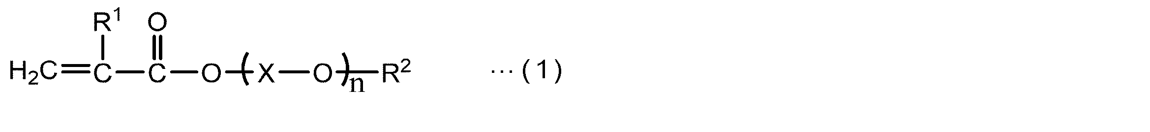


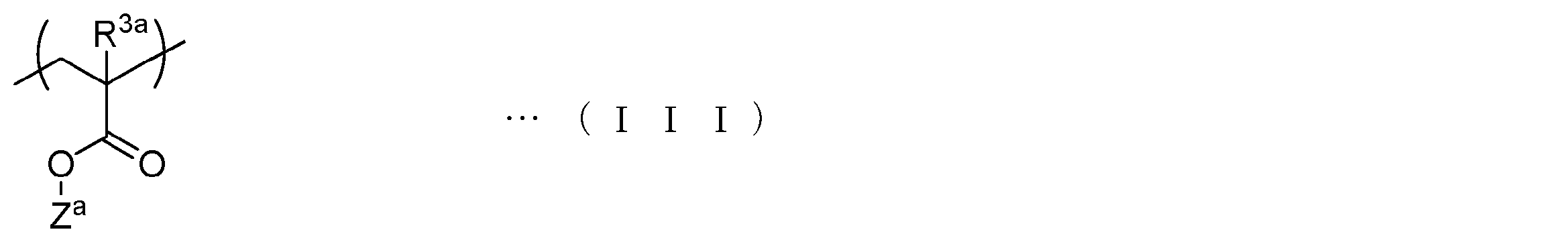
少なくとも2つの(メタ)アクリロイル基を有する化合物としては、例えば、(メタ)アクリル単量体及びそのオリゴマー((a)成分に該当する化合物を除く)が挙げられる。(b)成分の分子量(例えば、重量平均分子量)は、例えば、2万以下であってもよく、1万以下であってもよい。 ((B) Compound having at least two (meth) acryloyl groups)
Examples of the compound having at least two (meth) acryloyl groups include (meth) acrylic monomers and oligomers thereof (excluding compounds corresponding to the component (a)). The molecular weight (for example, weight average molecular weight) of the component (b) may be, for example, 20,000 or less or 10,000 or less.
(c)重合開始剤としては、例えば、(c1)熱重合開始剤(以下、場合により「(c1)成分」という)及び/又は(c2)光重合開始剤(以下、場合により「(c2)成分」という)を用いることができる。 ((C) polymerization initiator)
Examples of the (c) polymerization initiator include (c1) a thermal polymerization initiator (hereinafter, sometimes referred to as “(c1) component”) and / or (c2) a photopolymerization initiator (hereinafter, sometimes referred to as “(c2)”. Component)).
(d)成分であるフィラーとしては、無機フィラー、有機フィラー等が挙げられる。(d)成分としては、耐熱性若しくは熱伝導性を更に向上させる観点、溶融粘度を好適に調整する観点、又は、チキソトロピックック性を更に好適に付与する観点から、無機フィラーが好ましい。(d)成分は、1種を単独で又は2種以上を組み合わせて使用することができる。 ((D) filler)
(D) As a filler which is a component, an inorganic filler, an organic filler, etc. are mentioned. As the component (d), an inorganic filler is preferable from the viewpoint of further improving the heat resistance or thermal conductivity, the viewpoint of suitably adjusting the melt viscosity, or the viewpoint of further suitably imparting thixotropic properties. (D) A component can be used individually by 1 type or in combination of 2 or more types.
本実施形態に係る接着剤組成物は、必要に応じて、酸化防止剤を含有することができる。酸化防止剤としては、フェノール系酸化防止剤、チオエーテル系酸化防止剤、チオール系酸化防止剤等が挙げられる。酸化防止剤は、1種を単独で又は2種以上を組み合わせて使用することができる。 ((E) Antioxidant)
The adhesive composition according to the present embodiment can contain an antioxidant as necessary. Examples of the antioxidant include phenolic antioxidants, thioether antioxidants, and thiol antioxidants. Antioxidant can be used individually by 1 type or in combination of 2 or more types.
本実施形態に係る接着剤組成物は、カップリング剤を含有することができる。カップリング剤としては、特に制限はなく、シランカップリング剤、チタネート系カップリング剤、アルミニウム系カップリング剤、ジルコネート系カップリング剤、ジルコアルミネート系カップリング剤等の各種のカップリング剤を用いることができる。カップリング剤は、1種を単独で又は2種以上を組み合わせて使用することができる。 (Coupling agent)
The adhesive composition according to the present embodiment can contain a coupling agent. The coupling agent is not particularly limited, and various coupling agents such as a silane coupling agent, a titanate coupling agent, an aluminum coupling agent, a zirconate coupling agent, and a zircoaluminate coupling agent are used. be able to. A coupling agent can be used individually by 1 type or in combination of 2 or more types.
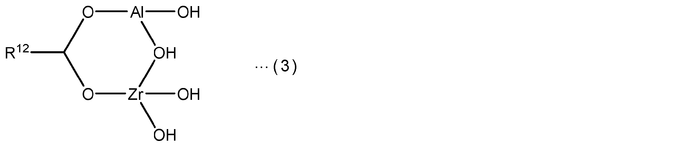
本実施形態に係る接着剤組成物は、エポキシ硬化剤を含有してもよい。エポキシ硬化剤は、エポキシ基を有する化合物と共に用いることができる。エポキシ硬化剤としては、特に制限はなく、エポキシ基を有する化合物と反応可能な化合物であればよい。エポキシ硬化剤の分子量は、100~400程度が好ましい。エポキシ硬化剤は、無色であること、又は、比較的着色していないこと(例えば、淡黄色であること)が好ましい。エポキシ硬化剤としては、酸無水物系硬化剤、イソシアヌル酸誘導体、フェノール系硬化剤等が挙げられる。エポキシ硬化剤は、1種を単独で又は2種以上を組み合わせて使用することができる。 (Epoxy curing agent)
The adhesive composition according to this embodiment may contain an epoxy curing agent. The epoxy curing agent can be used together with a compound having an epoxy group. There is no restriction | limiting in particular as an epoxy hardening | curing agent, What is necessary is just a compound which can react with the compound which has an epoxy group. The molecular weight of the epoxy curing agent is preferably about 100 to 400. The epoxy curing agent is preferably colorless or relatively uncolored (for example, light yellow). Examples of the epoxy curing agent include an acid anhydride curing agent, an isocyanuric acid derivative, and a phenol curing agent. An epoxy hardening | curing agent can be used individually by 1 type or in combination of 2 or more types.
本実施形態に係る接着剤組成物は、必要に応じて、エポキシ硬化促進剤を含有してもよい。エポキシ硬化促進剤としては、1,8-ジアザ-ビシクロ(5,4,0)ウンデセン-7、トリエチレンジアミン、トリ-2,4,6-ジメチルアミノメチルフェノール等の3級アミン類; 2-エチル-4メチルイミダゾール、2-メチルイミダゾール等のイミダゾール類; トリフェニルホスフィン、テトラフェニルホスホニウムテトラフェニルボレート、テトラ-n-ブチルホスホニウム-o,o-ジエチルホスホロジチオエート、テトラ-n-ブチルホスホニウム-テトラフルオロボレート、テトラ-n-ブチルホスホニウム-テトラフェニルボレート、メチルトリブチルホスホニウムジメチルホスフェート等のリン化合物; 4級アンモニウム塩; 有機金属塩類; これらの誘導体などを使用することができる。この中でも、接着剤組成物の安定性、透明性、及び、混合の容易さに更に優れる観点から、リン化合物が好ましい。エポキシ硬化促進剤は、1種を単独で又は2種以上を組み合わせて使用することができる。 (Epoxy curing accelerator)
The adhesive composition according to the present embodiment may contain an epoxy curing accelerator as necessary. Epoxy curing accelerators include tertiary amines such as 1,8-diaza-bicyclo (5,4,0) undecene-7, triethylenediamine, tri-2,4,6-dimethylaminomethylphenol; 2-ethyl Imidazoles such as -4 methylimidazole and 2-methylimidazole; triphenylphosphine, tetraphenylphosphonium tetraphenylborate, tetra-n-butylphosphonium-o, o-diethylphosphorodithioate, tetra-n-butylphosphonium-tetra Phosphorus compounds such as fluoroborate, tetra-n-butylphosphonium-tetraphenylborate, and methyltributylphosphonium dimethyl phosphate; quaternary ammonium salts; organometallic salts; and derivatives thereof can be used. Among these, a phosphorus compound is preferable from the viewpoint of further excellent stability, transparency, and ease of mixing of the adhesive composition. An epoxy hardening accelerator can be used individually by 1 type or in combination of 2 or more types.
本実施形態に係る接着剤組成物は、必要に応じて、有機溶媒を含有することができる。これにより、含有成分を有機溶媒に溶解又は分散させることによりワニス状の接着剤組成物を得ることができる。ワニス状の接着剤組成物は、基材への塗布性が向上し、作業性が良好である。 (Organic solvent)
The adhesive composition according to the present embodiment can contain an organic solvent as necessary. Thereby, a varnish-like adhesive composition can be obtained by melt | dissolving or disperse | distributing a component in an organic solvent. The varnish-like adhesive composition has improved workability and improved workability on the substrate.
本実施形態に係る接着剤組成物は、(b)成分とは別に、単官能(メタ)アクリル単量体(1つの(メタ)アクリロイル基を有する化合物)を含有してもよい。単官能(メタ)アクリル単量体としては、例えば、前記(a)成分で例示した(メタ)アクリル単量体((メタ)アクリル酸グリシジル等)が挙げられる。単官能(メタ)アクリル単量体は、1種を単独で又は2種以上を組み合わせて使用することができる。 (Other ingredients)
The adhesive composition according to this embodiment may contain a monofunctional (meth) acrylic monomer (a compound having one (meth) acryloyl group) separately from the component (b). Examples of the monofunctional (meth) acrylic monomer include the (meth) acrylic monomer exemplified by the component (a) (such as glycidyl (meth) acrylate). A monofunctional (meth) acryl monomer can be used individually by 1 type or in combination of 2 or more types.
本実施形態に係る接着剤組成物のチキソトロピック性(Thixotropic Index、「揺変度」ともいう)は、糸引きが発生しにくく、液の吐き出しが容易になることによりハンドリング性が向上する観点から、1.3以上が好ましく、1.4以上がより好ましい。チキソトロピック性の上限は、5.0以下が好ましく、4.0以下がより好ましい。本実施形態に係る接着剤組成物の粘性(T.I)は、例えば、以下に示す条件で、低速回転における粘度(25℃)及び高速回転における粘度(25℃)を測定し、次の式により算出される。
T.I=V2/V1
V1:高速回転時の粘度(P)
V2:低速回転時の粘度(P)
条件は、例えば、以下のとおりである。
(1)粘度計:EHD型粘度計(東機産業株式会社)
(2)コーン:3°コーン
(3)高速回転:5.0rpm/3min
(4)低速回転:0.5rpm/3min (Thixotropic (viscosity))
The thixotropic property (also referred to as “thixotropic index”) of the adhesive composition according to the present embodiment is less likely to cause stringing and from the viewpoint of improving handling properties by facilitating liquid discharge. 1.3 or more is preferable, and 1.4 or more is more preferable. The upper limit of thixotropic property is preferably 5.0 or less, and more preferably 4.0 or less. The viscosity (TI) of the adhesive composition according to the present embodiment is measured by, for example, measuring the viscosity at low speed rotation (25 ° C.) and the viscosity at high speed rotation (25 ° C.) under the following conditions. Is calculated by
T. T. et al. I = V2 / V1
V1: Viscosity at high speed (P)
V2: Viscosity at low speed (P)
The conditions are as follows, for example.
(1) Viscometer: EHD type viscometer (Toki Sangyo Co., Ltd.)
(2) Cone: 3 ° cone (3) High-speed rotation: 5.0 rpm / 3 min
(4) Low speed rotation: 0.5 rpm / 3 min
本実施形態に係る接着剤組成物は、前記の各含有成分を混合することにより得ることができる。フィラーを含有するワニス状の接着剤組成物を用いる場合、フィラーの分散性を考慮して、ライカイ機、3本ロール、ボールミル、ビーズミル等によって物理的なせん断力を与え、二次凝集した粒子が存在しないように充分に分散させた後に使用することが好ましい。前記の分散方法は、2種以上を組み合わせて使用することができる。 (Preparation of adhesive composition)
The adhesive composition according to this embodiment can be obtained by mixing each of the above-described components. When using a varnish-like adhesive composition containing a filler, in consideration of the dispersibility of the filler, a physical shearing force is applied by a lykai machine, three rolls, a ball mill, a bead mill, etc. It is preferably used after being sufficiently dispersed so that it does not exist. The above dispersion methods can be used in combination of two or more.
本実施形態に係る半導体装置の製造方法は、本実施形態に係る接着剤組成物を含む接着剤層が半導体基板と透明基材との間に配置された状態で前記接着剤層を硬化する工程を備える。例えば、本実施形態に係る半導体装置の製造方法は、本実施形態に係る接着剤組成物を含む接着剤層(接着樹脂層)を半導体基板上に形成する工程(接着剤層形成工程)と、前記接着剤層が前記半導体基板と透明基材との間に配置された状態で前記接着剤層を硬化する工程(硬化物形成工程)と、を備える。接着剤層は、例えば、本実施形態に係る接着剤組成物からなる。透明基材(ガラス基材等)は、例えば、透明基板(ガラス基板等)である。硬化物形成工程は、接着剤層を半導体基板と透明基材とで挟み、前記半導体基板及び前記透明基材を圧着する工程(圧着工程)と、接着剤層を硬化する工程(硬化工程)とを有していてもよい。圧着工程及び硬化工程は、必ずしも独立した工程である必要はなく、圧着を行いながら同時に硬化を行ってもよい。 <Method for Manufacturing Semiconductor Device>
The manufacturing method of the semiconductor device according to the present embodiment includes a step of curing the adhesive layer in a state where the adhesive layer including the adhesive composition according to the present embodiment is disposed between the semiconductor substrate and the transparent substrate. Is provided. For example, the method for manufacturing a semiconductor device according to the present embodiment includes a step of forming an adhesive layer (adhesive resin layer) containing the adhesive composition according to the present embodiment on a semiconductor substrate (adhesive layer forming step), A step of curing the adhesive layer in a state where the adhesive layer is disposed between the semiconductor substrate and the transparent substrate (cured material forming step). The adhesive layer is made of, for example, an adhesive composition according to this embodiment. A transparent substrate (glass substrate etc.) is a transparent substrate (glass substrate etc.), for example. The cured product forming step includes sandwiching the adhesive layer between the semiconductor substrate and the transparent base material, crimping the semiconductor substrate and the transparent base material (crimping step), and curing the adhesive layer (curing step). You may have. The crimping process and the curing process are not necessarily independent processes, and curing may be performed simultaneously while performing the crimping.
接着剤層形成工程としては、例えば、本実施形態に係る接着剤組成物を半導体基板上に塗布する方法、又は、フィルム状の接着剤組成物を半導体基板に貼り付ける方法を採用することができる。半導体基板は、半導体ウェハ、及び、半導体素子(半導体チップ)のいずれであってもよい。 (Adhesive layer forming process)
As the adhesive layer forming step, for example, a method of applying the adhesive composition according to the present embodiment on a semiconductor substrate or a method of attaching a film-like adhesive composition to a semiconductor substrate can be employed. . The semiconductor substrate may be either a semiconductor wafer or a semiconductor element (semiconductor chip).
続いて、半導体基板上に形成された接着剤層を、必要に応じて加熱乾燥する。乾燥する温度に特に制限はないが、含有成分を溶媒に溶解又は分散させてワニス状の接着剤組成物を用いる場合、乾燥温度は、溶媒の発泡により気泡が発生することを乾燥時に抑制しやすい観点から、使用した溶媒の沸点よりも10~50℃低いことが好ましい。同様の観点から、乾燥温度は、使用した溶媒の沸点よりも15~45℃低いことがより好ましく、使用した溶媒の沸点よりも20~40℃低いことが更に好ましい。 (Crimping process)
Subsequently, the adhesive layer formed on the semiconductor substrate is heat-dried as necessary. The drying temperature is not particularly limited, but when the varnish-like adhesive composition is used by dissolving or dispersing the components in a solvent, the drying temperature is likely to suppress the generation of bubbles due to foaming of the solvent during drying. From the viewpoint, it is preferably 10 to 50 ° C. lower than the boiling point of the solvent used. From the same viewpoint, the drying temperature is more preferably 15 to 45 ° C. lower than the boiling point of the solvent used, and further preferably 20 to 40 ° C. lower than the boiling point of the solvent used.
接着剤層を介して半導体基板と透明基材とを圧着した後、接着剤層を硬化させることにより硬化物を形成する。硬化方法としては、例えば、熱及び/又は光により硬化させる方法が挙げられ、特に、熱により硬化させることが好ましい。 (Curing process)
After pressure-bonding the semiconductor substrate and the transparent substrate via the adhesive layer, the cured product is formed by curing the adhesive layer. Examples of the curing method include a method of curing with heat and / or light, and it is particularly preferable to cure with heat.
本実施形態に係る接着剤層の硬化物のガラス転移温度(Tg)は、-10℃以上が好ましく、0℃以上がより好ましい。 <Physical properties of the cured adhesive layer>
The glass transition temperature (Tg) of the cured product of the adhesive layer according to this embodiment is preferably −10 ° C. or higher, and more preferably 0 ° C. or higher.
本実施形態に係る半導体装置は、半導体基板と、前記半導体基板上に配置された接着剤層と、前記接着剤層を介して前記半導体基板に接着された透明基材と、を備える。前記接着剤層は、本実施形態に係る接着剤組成物又はその硬化物を含む。前記透明基材は、例えば、接着剤層を介して半導体基板上に配置されている。半導体装置としては、例えば、光学部品が挙げられる。光学部品としては、例えば、固体撮像素子等の光デバイスが挙げられる。固体撮像素子としては、CCDイメージセンサ、CMOSイメージセンサ等が挙げられる。固体撮像素子は、例えば、上面に受光部が配置された半導体基板と、前記受光部を覆うように前記半導体基板上に配置された接着剤層と、前記接着剤層を介して前記半導体基板に接着された透明基材と、を備える。 <Semiconductor device>
The semiconductor device according to the present embodiment includes a semiconductor substrate, an adhesive layer disposed on the semiconductor substrate, and a transparent base material bonded to the semiconductor substrate via the adhesive layer. The adhesive layer includes the adhesive composition according to the present embodiment or a cured product thereof. The said transparent base material is arrange | positioned on the semiconductor substrate through the adhesive bond layer, for example. Examples of the semiconductor device include an optical component. Examples of the optical component include an optical device such as a solid-state image sensor. Examples of the solid-state imaging device include a CCD image sensor and a CMOS image sensor. For example, the solid-state imaging device includes a semiconductor substrate having a light receiving portion disposed on an upper surface, an adhesive layer disposed on the semiconductor substrate so as to cover the light receiving portion, and the semiconductor substrate via the adhesive layer. And a bonded transparent substrate.
表1,2の成分を表1,2の配合割合(質量部)で混合し、実施例1~18及び比較例1~2の接着剤組成物の溶液を得た。表1,2中の各成分は、以下に示すものである。 <Preparation of adhesive composition>
The components shown in Tables 1 and 2 were mixed in the mixing ratios (parts by mass) shown in Tables 1 and 2 to obtain solutions of the adhesive compositions of Examples 1 to 18 and Comparative Examples 1 and 2. Each component in Tables 1 and 2 is shown below.
(a)成分である(メタ)アクリル重合体(a-1)及び(メタ)アクリル重合体(a-2)は、下記の手順で合成した。 ((Meth) acrylic polymer)
The component (a) (meth) acrylic polymer (a-1) and (meth) acrylic polymer (a-2) were synthesized by the following procedure.
アクリル酸トリシクロ[5.2.1.02,6]デカ-8-イル(FA-513A、日立化成株式会社、商品名)300g、アクリル酸ブチル(BA)350g、メタクリル酸ブチル(BMA)300g、メタクリル酸グリシジル(GMA)50g及びメタクリル酸2-エチルヘキシル(2EHMA)50gを混合して単量体混合物を得た。得られた単量体混合物にジラウロイルパーオキサイド5g及びn-オクチルメルカプタン(連鎖移動剤)0.45gを溶解させて、混合液を得た。 [(Meth) acrylic polymer (a-1)]
Tricyclo [5.2.1.0 2,6 ] dec-8-yl acrylate (FA-513A, Hitachi Chemical Co., Ltd., trade name) 300 g, butyl acrylate (BA) 350 g, butyl methacrylate (BMA) 300 g Then, 50 g of glycidyl methacrylate (GMA) and 50 g of 2-ethylhexyl methacrylate (2EHMA) were mixed to obtain a monomer mixture. Dilauroyl peroxide (5 g) and n-octyl mercaptan (chain transfer agent) (0.45 g) were dissolved in the obtained monomer mixture to obtain a mixed solution.
アクリル酸トリシクロ[5.2.1.02,6]デカ-8-イル(FA-513A、日立化成株式会社、商品名)220g、アクリル酸ブチル(BA)165g、メタクリル酸ブチル(BMA)250g、メタクリル酸グリシジル(GMA)200g及びメタクリル酸2-エチルヘキシル(2EHMA)165gを混合した以外は(メタ)アクリル重合体(a-1)と同様の方法によって(メタ)アクリル重合体(a-2)を得た。得られた(メタ)アクリル重合体(a-2)の重量平均分子量は52万であった。 [(Meth) acrylic polymer (a-2)]
Tricyclo [5.2.1.0 2,6 ] dec-8-yl acrylate (FA-513A, Hitachi Chemical Co., Ltd., trade name) 220 g, butyl acrylate (BA) 165 g, butyl methacrylate (BMA) 250 g (Meth) acrylic polymer (a-2) by the same method as (meth) acrylic polymer (a-1) except that 200 g of glycidyl methacrylate (GMA) and 165 g of 2-ethylhexyl methacrylate (2EHMA) were mixed Got. The obtained (meth) acrylic polymer (a-2) had a weight average molecular weight of 520,000.
ポンプ:L6000 Pump(株式会社日立製作所)
検出器:L3300 RI Monitor(株式会社日立製作所)
カラム:Gelpack GL-S300MDT-5(計2本)(日立化成株式会社、商品名)
カラムサイズ:直径8mm×300mm
溶離液:DMF/THF(質量比1/1)+LiBr・H2O 0.03mol/L+H3PO4 0.06mol/L
試料濃度:0.1質量%
流量:1mL/min
測定温度:40℃ The weight average molecular weight of component (a) was converted from a calibration curve using standard polystyrene by gel permeation chromatography (GPC). The calibration curve was approximated by a cubic equation using a standard polystyrene kit PStQuick series C (Tosoh Corporation, trade name). The GPC conditions are shown below.
Pump: L6000 Pump (Hitachi, Ltd.)
Detector: L3300 RI Monitor (Hitachi, Ltd.)
Column: Gelpack GL-S300MDT-5 (2 in total) (Hitachi Chemical Co., Ltd., trade name)
Column size: Diameter 8mm x 300mm
Eluent: DMF / THF (
Sample concentration: 0.1% by mass
Flow rate: 1 mL / min
Measurement temperature: 40 ° C
ジオキサングリコールジアクリレート(商品名:「A-DOG」(新中村化学工業株式会社))
トリシクロデカンジメタノールジアクリレート(商品名:「A-DCP」(新中村化学工業株式会社))
メタクリル酸グリシジル(GMA、市販品:シグマアルドリッチ社) ((Meth) acrylic monomer)
Dioxane glycol diacrylate (trade name: “A-DOG” (Shin Nakamura Chemical Co., Ltd.))
Tricyclodecane dimethanol diacrylate (trade name: “A-DCP” (Shin Nakamura Chemical Co., Ltd.))
Glycidyl methacrylate (GMA, commercial product: Sigma-Aldrich)
パークミルD(商品名、日油株式会社、熱重合開始剤、ジクミルパーオキサイド、1時間半減期温度135.7℃、10時間半減期温度116.4℃) (Polymerization initiator)
Park Mill D (trade name, NOF Corporation, thermal polymerization initiator, dicumyl peroxide, 1 hour half-life temperature 135.7 ° C., 10 hour half-life temperature 116.4 ° C.)
RY200(商品名、日本アエロジル株式会社製、ナノシリカフィラー(非晶性シリカ)、平均粒子径12nm)
R972(商品名、日本アエロジル株式会社製、ナノシリカフィラー(非晶性シリカ)、平均粒子径16nm)
SE-2050-SMJ(商品名、株式会社アドマテックス製、シリカフィラー(非晶性シリカ)、平均粒子径500nm、最大粒子径3000nm)
CF0093(商品名、日本フリット株式会社製、ガラスフィラー、平均粒子径3000nm)
CF0023(商品名、日本フリット株式会社製、ガラスフィラー、平均粒子径10000nm)
前記「ガラスフィラー」は、SiO2を含み、ZrO2、B2O3、Na2O、F2、Al2O3、CaO、MgO、SrO等を一定の割合で含む。 (Filler)
RY200 (trade name, manufactured by Nippon Aerosil Co., Ltd., nano silica filler (amorphous silica),
R972 (trade name, manufactured by Nippon Aerosil Co., Ltd., nano silica filler (amorphous silica), average particle size 16 nm)
SE-2050-SMJ (trade name, manufactured by Admatechs Co., Ltd., silica filler (amorphous silica), average particle size 500 nm, maximum particle size 3000 nm)
CF0093 (trade name, manufactured by Nippon Frit Co., Ltd., glass filler, average particle size 3000 nm)
CF0023 (trade name, manufactured by Nippon Frit Co., Ltd., glass filler, average particle size 10,000 nm)
The “glass filler” contains SiO 2 and contains ZrO 2 , B 2 O 3 , Na 2 O, F 2 , Al 2 O 3 , CaO, MgO, SrO and the like at a certain ratio.
アデカスタブAO-80(商品名、株式会社ADEKA、ヒンダードフェノール系酸化防止剤、ビス[3-(3-tert-ブチル-4-ヒドロキシ-5-メチルフェニル)プロピオン酸](2,4,8,10-テトラオキサスピロ[5.5]ウンデカン-3,9-ジイル)ビス(2,2-ジメチル-2,1-エタンジイル)
アデカスタブAO-503(商品名、株式会社ADEKA、チオエーテル系酸化防止剤、3,3-チオビスプロピオン酸ジトリデシル)
カレンズMT-NR1(商品名、共栄社化学株式会社、1,3,5-トリス(3-メルカプトブチリルオキシエチル)-1,3,5-トリアジン-2,4,6(1H,3H,5H)-トリオン) (Antioxidant)
ADK STAB AO-80 (trade name, ADEKA Corporation, hindered phenol antioxidant, bis [3- (3-tert-butyl-4-hydroxy-5-methylphenyl) propionic acid] (2, 4, 8, 10-tetraoxaspiro [5.5] undecane-3,9-diyl) bis (2,2-dimethyl-2,1-ethanediyl)
ADK STAB AO-503 (trade name, ADEKA Corporation, thioether antioxidant,
Karenz MT-NR1 (trade name, Kyoeisha Chemical Co., Ltd., 1,3,5-tris (3-mercaptobutyryloxyethyl) -1,3,5-triazine-2,4,6 (1H, 3H, 5H) -Trion)
カップリング剤(密着助剤):メタクリル酸3-(トリメトキシシリル)プロピル(シランカップリング剤、信越化学工業株式会社、商品名:KBM-503)
エポキシ硬化剤:3or4-メチル-ヘキサヒドロ無水フタル酸(日立化成株式会社、商品名:HN-5500)
エポキシ硬化促進剤:メチルトリブチルホスホニウムジメチルホスフェート(日本化学工業株式会社、商品名:ヒシコーリンPX-4MP)
溶媒:PGMEA(関東化学株式会社、化学物質名:プロピレングリコール1-モノメチルエーテル2-アセテート) (Other)
Coupling agent (adhesion aid): 3- (trimethoxysilyl) propyl methacrylate (silane coupling agent, Shin-Etsu Chemical Co., Ltd., trade name: KBM-503)
Epoxy curing agent: 3or4-methyl-hexahydrophthalic anhydride (Hitachi Chemical Co., Ltd., trade name: HN-5500)
Epoxy curing accelerator: methyltributylphosphonium dimethyl phosphate (Nippon Chemical Industry Co., Ltd., trade name: Hishicolin PX-4MP)
Solvent: PGMEA (Kanto Chemical Co., Inc., chemical name: propylene glycol 1-monomethyl ether 2-acetate)
(チキソトロピック性)
チキソトロピック性(Thixotropic Index、「揺変度」ともいう)とは、所定の粘度計及びコーンにより高速回転と低速回転とにおける試料の粘度を測定し、高速回転時の粘度と低速回転時の粘度との比をいう。以下に示す条件で低速回転における粘度及び高速回転における粘度を測定し、次の式によりチキソトロピック性(T.I)を算出した。
T.I=V2/V1
V1:高速回転時の粘度(P)
V2:低速回転時の粘度(P)
以下の測定条件を採用した。
(1)粘度計:EHD型粘度計(東機産業株式会社)
(2)コーン:3°コーン
(3)高速回転:5.0rpm/3min
(4)低速回転:0.5rpm/3min
チキソトロピック性が1.3以上である場合を「A」と評価し、1.3未満である場合を「B」と評価した。評価結果を表1,2に示す。 <Evaluation>
(Thixotropic properties)
Thixotropic index (also referred to as “thickness”) is a measurement of the viscosity of a sample at high speed and low speed using a predetermined viscometer and cone, and the viscosity at high speed and low speed. And the ratio. The viscosity at low speed rotation and the viscosity at high speed rotation were measured under the following conditions, and thixotropic property (TI) was calculated by the following equation.
T. T. et al. I = V2 / V1
V1: Viscosity at high speed (P)
V2: Viscosity at low speed (P)
The following measurement conditions were adopted.
(1) Viscometer: EHD type viscometer (Toki Sangyo Co., Ltd.)
(2) Cone: 3 ° cone (3) High-speed rotation: 5.0 rpm / 3 min
(4) Low speed rotation: 0.5 rpm / 3 min
The case where the thixotropic property was 1.3 or more was evaluated as “A”, and the case where it was less than 1.3 was evaluated as “B”. The evaluation results are shown in Tables 1 and 2.
アプリケーターを用いて実施例及び比較例の接着剤組成物を離型PETフィルムに塗布した後に100℃/10分で乾燥させることにより、膜厚100μmのフィルム状の樹脂膜を作製した。次に、ロールラミネーターを使用して90℃で離型PETフィルムを貼り付けることにより、PETフィルム/樹脂膜/PETフィルムの3層構造の積層体を得た。離型PETフィルムとしては、藤森工業株式会社製のフィルムバイナ38E-0010GCを用いた。その後、樹脂膜を150℃で1時間、180℃で1時間硬化した。フィルム状の硬化膜をPETフィルムから剥がして単膜の硬化膜を得た。25℃における硬化膜の透過率を測定した。具体的には、分光光度計U4100(商品名、株式会社日立製作所、開始800nm、終了300nm、スキャンスピード600nm/min、サンプリング間隔1.0nm)を用いて、波長800~300nmの範囲で透過率を測定した。なお、ベースラインはAirとした。測定結果を下記の判定基準に従って評価した。評価結果を表1,2に示す。
A:波長400nmにおける透過率が90%以上。
B:波長400nmにおける透過率が85%以上90%未満。
C:波長400nmにおける透過率が85%未満。 (Transmittance)
The adhesive compositions of Examples and Comparative Examples were applied to a release PET film using an applicator and then dried at 100 ° C./10 minutes to prepare a film-like resin film having a thickness of 100 μm. Next, a laminate having a three-layer structure of PET film / resin film / PET film was obtained by attaching a release PET film at 90 ° C. using a roll laminator. A film binder 38E-0010GC manufactured by Fujimori Kogyo Co., Ltd. was used as the release PET film. Thereafter, the resin film was cured at 150 ° C. for 1 hour and at 180 ° C. for 1 hour. The film-like cured film was peeled off from the PET film to obtain a single film cured film. The transmittance of the cured film at 25 ° C. was measured. Specifically, using a spectrophotometer U4100 (trade name, Hitachi, Ltd., start 800 nm, end 300 nm, scan speed 600 nm / min, sampling interval 1.0 nm), transmittance is measured in the wavelength range of 800 to 300 nm. It was measured. The baseline was Air. The measurement results were evaluated according to the following criteria. The evaluation results are shown in Tables 1 and 2.
A: The transmittance at a wavelength of 400 nm is 90% or more.
B: The transmittance at a wavelength of 400 nm is 85% or more and less than 90%.
C: The transmittance at a wavelength of 400 nm is less than 85%.
アプリケーターを用いて実施例の接着剤組成物を離型PETフィルムに塗布した後に100℃/10分で乾燥させることにより、膜厚100μmのフィルム状の樹脂膜を作製した。次に、ロールラミネーターを使用して90℃で離型PETフィルムを貼り付けることにより、PETフィルム/樹脂膜/PETフィルムの3層構造の積層体を得た。離型PETフィルムとしては、藤森工業株式会社製のフィルムバイナ38E-0010GCを用いた。その後、樹脂膜を150℃で1時間、180℃で1時間硬化した。フィルム状の硬化膜をPETフィルムから剥がして単膜の硬化膜を得た。硬化膜の屈折率を測定した。具体的には、硬化膜を多波長アッベ屈折計(株式会社アタゴ製、DR-M2(商品名))の主プリズム上に置き、採光ガラス及びモノブロモナフタレン溶液(干渉液)を用いて、25℃における屈折率(波長589.3nm(ナトリウムのD線))を測定した。測定は透過式で行った。屈折計に付属の恒温水槽の温度を調整して硬化膜の温度を調整した。「アッベ屈折計」は、臨界角の位置をとらえて屈折率を求める屈折計である。屈折率は、いずれも1.49~1.50であった。 (Refractive index)
The adhesive composition of the example was applied to a release PET film using an applicator and then dried at 100 ° C./10 minutes to prepare a film-like resin film having a thickness of 100 μm. Next, a laminate having a three-layer structure of PET film / resin film / PET film was obtained by attaching a release PET film at 90 ° C. using a roll laminator. A film binder 38E-0010GC manufactured by Fujimori Kogyo Co., Ltd. was used as the release PET film. Thereafter, the resin film was cured at 150 ° C. for 1 hour and at 180 ° C. for 1 hour. The film-like cured film was peeled off from the PET film to obtain a single film cured film. The refractive index of the cured film was measured. Specifically, the cured film is placed on the main prism of a multi-wavelength Abbe refractometer (manufactured by Atago Co., Ltd., DR-M2 (trade name)), and is obtained using a daylighting glass and a monobromonaphthalene solution (interference liquid). The refractive index (wavelength 589.3 nm (sodium D line)) at 0 ° C. was measured. The measurement was performed by a transmission method. The temperature of the constant temperature water tank attached to the refractometer was adjusted to adjust the temperature of the cured film. The “Abbe refractometer” is a refractometer that obtains the refractive index by capturing the position of the critical angle. The refractive indexes were all 1.49 to 1.50.
スピンコーターを用いて実施例の接着剤組成物を厚さ400μmのシリコンウエハ上に均一に塗布した後に100℃のホットプレートで10分間乾燥させることにより、膜厚50μmの接着剤層を備える試験基板を作製した。得られた試験基板の接着剤層に、4.0cm×5.0cm×120~170μm(実測140~160μm)のガラス基板(MATSUNAMI MICRO COVER GLASS 40mm×50mm THICKNESS No.1:松浪硝子工業株式会社、商品名)を、ロールラミネーターを用いて貼り付けた後、150℃で1時間、180℃で1時間加熱して硬化させた。この試験基板を260℃の熱板上で30秒間放置した後、室温(25℃)に戻して5分間保持する操作を行った。そして、試験基板の外観を目視にて観察した。いずれも外観異常は確認されなかった。 (Reflow resistance)
A test substrate provided with an adhesive layer having a thickness of 50 μm by uniformly applying the adhesive composition of the example onto a 400 μm-thick silicon wafer using a spin coater and then drying it on a hot plate at 100 ° C. for 10 minutes. Was made. To the adhesive layer of the obtained test substrate, a glass substrate of 4.0 cm × 5.0 cm × 120 to 170 μm (actual measurement 140 to 160 μm) (MATSANAMI MICRO COVER GLASS 40 mm × 50 mm TICHKNESS No. 1: Matsunami Glass Industrial Co., Ltd., (Product name) was pasted using a roll laminator, and then cured by heating at 150 ° C. for 1 hour and at 180 ° C. for 1 hour. The test substrate was allowed to stand on a hot plate at 260 ° C. for 30 seconds, and then returned to room temperature (25 ° C.) and held for 5 minutes. And the external appearance of the test board | substrate was observed visually. None of the appearance abnormalities were confirmed.
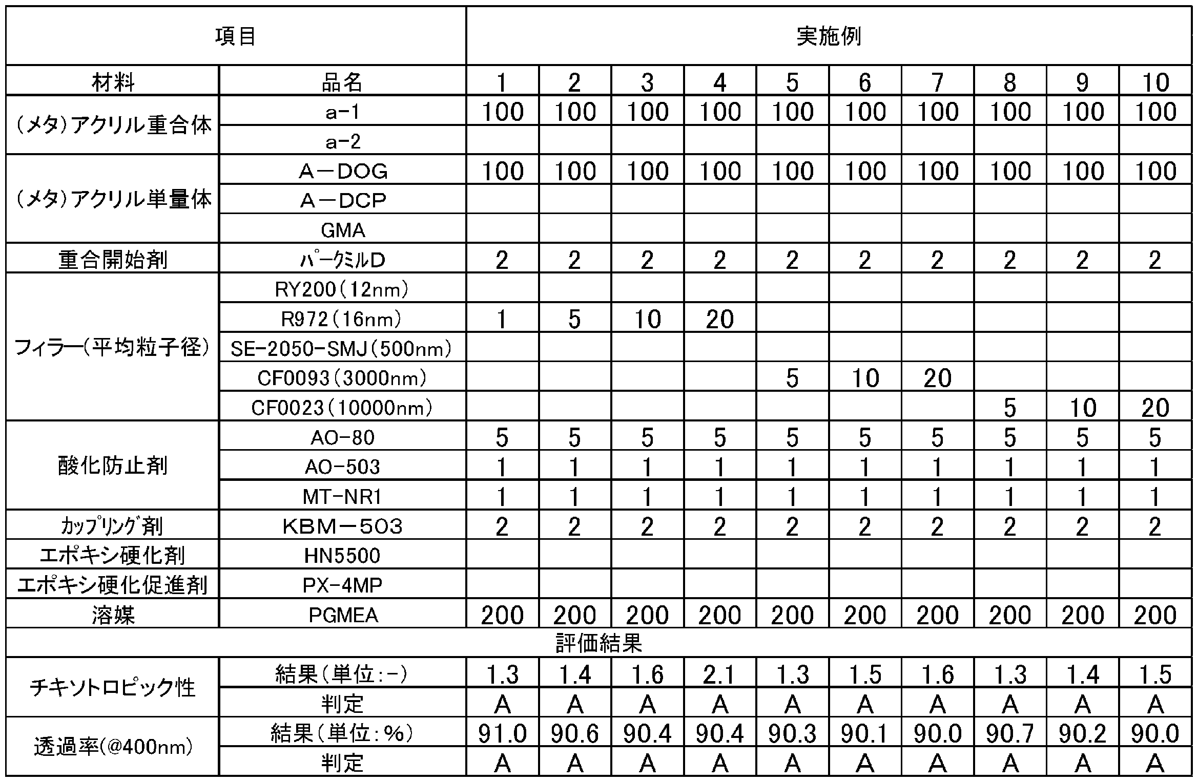
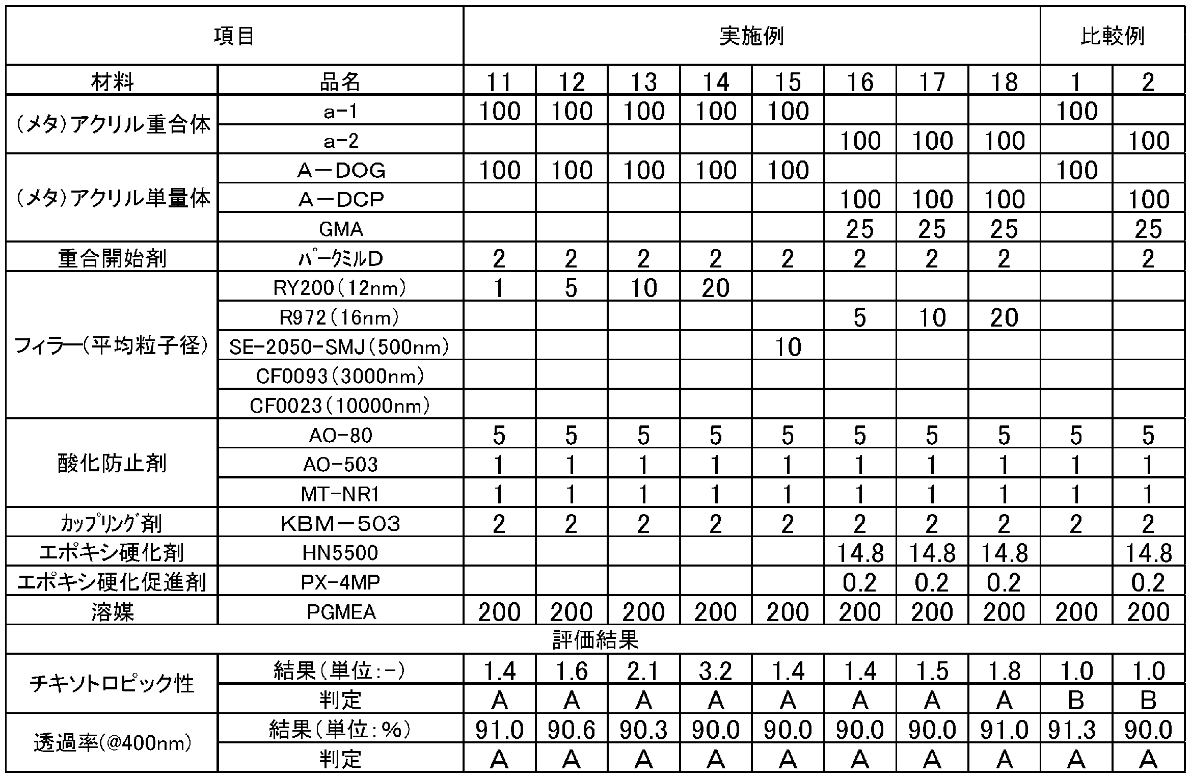
Claims (11)
- (a)(メタ)アクリル重合体と、(b)少なくとも2つの(メタ)アクリロイル基を有する化合物と、(c)重合開始剤と、(d)フィラーと、を含有する、接着剤組成物。 An adhesive composition comprising (a) a (meth) acrylic polymer, (b) a compound having at least two (meth) acryloyl groups, (c) a polymerization initiator, and (d) a filler.
- 前記(d)成分の含有量が、前記(a)成分及び前記(b)成分の総量100質量部に対して0.1~40質量部である、請求項1に記載の接着剤組成物。 The adhesive composition according to claim 1, wherein the content of the component (d) is 0.1 to 40 parts by mass with respect to 100 parts by mass of the total amount of the component (a) and the component (b).
- 前記(d)成分の平均粒子径が5~10000nmである、請求項1又は2に記載の接着剤組成物。 The adhesive composition according to claim 1 or 2, wherein the component (d) has an average particle size of 5 to 10,000 nm.
- 前記(a)成分が脂環式構造を有する、請求項1~3のいずれか一項に記載の接着剤組成物。 The adhesive composition according to any one of claims 1 to 3, wherein the component (a) has an alicyclic structure.
- 前記(a)成分がエポキシ基を有する、請求項1~4のいずれか一項に記載の接着剤組成物。 The adhesive composition according to any one of claims 1 to 4, wherein the component (a) has an epoxy group.
- 前記(a)成分が、下記一般式(I)で表される構造単位を有する、請求項1~5のいずれか一項に記載の接着剤組成物。
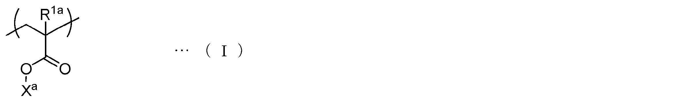
- 酸化防止剤を更に含有する、請求項1~6のいずれか一項に記載の接着剤組成物。 The adhesive composition according to any one of claims 1 to 6, further comprising an antioxidant.
- 光学部品用である、請求項1~7のいずれか一項に記載の接着剤組成物。 The adhesive composition according to any one of claims 1 to 7, which is used for optical parts.
- 請求項1~8のいずれか一項に記載の接着剤組成物の硬化物。 A cured product of the adhesive composition according to any one of claims 1 to 8.
- 請求項1~8のいずれか一項に記載の接着剤組成物を含む接着剤層を半導体基板上に形成する工程と、
前記接着剤層が前記半導体基板と透明基材との間に配置された状態で前記接着剤層を硬化する工程と、を備える、半導体装置の製造方法。 Forming an adhesive layer comprising the adhesive composition according to any one of claims 1 to 8 on a semiconductor substrate;
And a step of curing the adhesive layer in a state where the adhesive layer is disposed between the semiconductor substrate and the transparent base material. - 半導体基板と、
前記半導体基板上に配置された接着剤層と、
前記接着剤層を介して前記半導体基板に接着された透明基材と、を備え、
前記接着剤層が、請求項1~8のいずれか一項に記載の接着剤組成物又はその硬化物を含む、半導体装置。 A semiconductor substrate;
An adhesive layer disposed on the semiconductor substrate;
A transparent base material bonded to the semiconductor substrate via the adhesive layer,
A semiconductor device, wherein the adhesive layer comprises the adhesive composition according to any one of claims 1 to 8 or a cured product thereof.
Priority Applications (4)
| Application Number | Priority Date | Filing Date | Title |
|---|---|---|---|
| KR1020187003647A KR102479906B1 (en) | 2015-07-29 | 2016-07-27 | Adhesive composition, cured product, semiconductor device and manufacturing method thereof |
| US15/747,967 US10947326B2 (en) | 2015-07-29 | 2016-07-27 | Adhesive composition, cured article, semiconductor device, and production method for same |
| JP2017530906A JP6809461B2 (en) | 2015-07-29 | 2016-07-27 | Adhesive composition, cured product, semiconductor device and its manufacturing method |
| CN201680043964.1A CN107849417B (en) | 2015-07-29 | 2016-07-27 | Adhesive composition, cured product, semiconductor device, and method for producing same |
Applications Claiming Priority (2)
| Application Number | Priority Date | Filing Date | Title |
|---|---|---|---|
| JP2015-150041 | 2015-07-29 | ||
| JP2015150041 | 2015-07-29 |
Publications (1)
| Publication Number | Publication Date |
|---|---|
| WO2017018459A1 true WO2017018459A1 (en) | 2017-02-02 |
Family
ID=57884703
Family Applications (1)
| Application Number | Title | Priority Date | Filing Date |
|---|---|---|---|
| PCT/JP2016/072060 WO2017018459A1 (en) | 2015-07-29 | 2016-07-27 | Adhesive composition, cured article, semiconductor device, and production method for same |
Country Status (6)
| Country | Link |
|---|---|
| US (1) | US10947326B2 (en) |
| JP (1) | JP6809461B2 (en) |
| KR (1) | KR102479906B1 (en) |
| CN (1) | CN107849417B (en) |
| TW (1) | TWI716426B (en) |
| WO (1) | WO2017018459A1 (en) |
Cited By (2)
| Publication number | Priority date | Publication date | Assignee | Title |
|---|---|---|---|---|
| JP2020041108A (en) * | 2018-09-13 | 2020-03-19 | 東洋インキScホールディングス株式会社 | Active energy ray-polymerizable adhesive for optical use, and optical laminate |
| WO2023127551A1 (en) * | 2021-12-28 | 2023-07-06 | 東洋紡株式会社 | Curable resin composition and hot melt adhesive |
Families Citing this family (3)
| Publication number | Priority date | Publication date | Assignee | Title |
|---|---|---|---|---|
| US11114483B2 (en) * | 2018-08-10 | 2021-09-07 | Omnivision Technologies, Inc. | Cavityless chip-scale image-sensor package |
| JP7163221B2 (en) * | 2019-03-11 | 2022-10-31 | キオクシア株式会社 | Polymer material, composition and method for manufacturing semiconductor device |
| CN117511426B (en) * | 2024-01-05 | 2024-04-12 | 深圳市长松科技有限公司 | Film for packaging and blocking water vapor, semiconductor film packaging method and structure |
Citations (7)
| Publication number | Priority date | Publication date | Assignee | Title |
|---|---|---|---|---|
| JP2008277806A (en) * | 2007-04-05 | 2008-11-13 | Hitachi Chem Co Ltd | Adhesive member for semiconductor, semiconductor device and method for manufacturing the semiconductor device |
| JP2009015309A (en) * | 2007-05-25 | 2009-01-22 | Sumitomo Bakelite Co Ltd | Resin composition, resin spacer film, and semiconductor device |
| JP2010254869A (en) * | 2009-04-28 | 2010-11-11 | Bridgestone Corp | Photocurable self-adhesive sheet and method for forming photocurable self-adhesive layer by using the same |
| JP2013028733A (en) * | 2011-07-29 | 2013-02-07 | Sumitomo Bakelite Co Ltd | Liquid resin composition, and semiconductor device |
| JP2013118230A (en) * | 2011-12-01 | 2013-06-13 | Canon Inc | Solid-state imaging device |
| JP2014156585A (en) * | 2013-01-16 | 2014-08-28 | Cemedine Co Ltd | Photocurable composition |
| WO2015115553A1 (en) * | 2014-01-29 | 2015-08-06 | 日立化成株式会社 | Adhesive composition, method for manufacturing semiconductor device using adhesive composition, and solid-state imaging element |
Family Cites Families (28)
| Publication number | Priority date | Publication date | Assignee | Title |
|---|---|---|---|---|
| US4968559A (en) * | 1985-02-14 | 1990-11-06 | Bando Chemical Industries. Ltd. | Pressure sensitive adhesive film with barrier layer |
| US20020156144A1 (en) * | 2001-02-09 | 2002-10-24 | Williams Kevin Alan | UV-curable, non-chlorinated adhesion promoters |
| JP2005120206A (en) * | 2003-10-16 | 2005-05-12 | Sumitomo Bakelite Co Ltd | Adhesive film for semiconductor, dicing film, and semiconductor device |
| JP4046067B2 (en) | 2003-11-04 | 2008-02-13 | ソニー株式会社 | Manufacturing method of solid-state imaging device |
| JP2005327789A (en) * | 2004-05-12 | 2005-11-24 | Sharp Corp | Pressure-sensitive adhesive sheet for both dicing and die-bonding, and method of manufacturing semiconductor device using the same |
| KR100657896B1 (en) * | 2004-08-20 | 2006-12-14 | 삼성전자주식회사 | A method of storing substrate having immobilized reactive groups or probe molecules method of producing microarray using the UV film and a substrate having attached UV film |
| US7297370B2 (en) * | 2004-12-22 | 2007-11-20 | General Electric Company | Curable encapsulant composition, device including same, and associated method |
| JP4466397B2 (en) * | 2005-02-10 | 2010-05-26 | 住友ベークライト株式会社 | Adhesive film for semiconductor and semiconductor device using the same |
| JP2008003541A (en) * | 2006-01-27 | 2008-01-10 | Fujifilm Corp | Polarizer protective film, and polarizer and liquid crystal display using the same |
| JP4923689B2 (en) | 2006-04-11 | 2012-04-25 | ソニー株式会社 | Solid-state imaging device and method for manufacturing solid-state imaging device |
| US8194210B2 (en) * | 2006-10-26 | 2012-06-05 | Fujifilm Corporation | Polarizing plate protective film, polarizing plate and liquid crystal display device |
| JP2011513995A (en) * | 2008-03-07 | 2011-04-28 | スリーエム イノベイティブ プロパティズ カンパニー | Dicing tape and die attach adhesive with patterned backing |
| JP5342174B2 (en) * | 2008-05-23 | 2013-11-13 | 日東電工株式会社 | Adhesive composition and use thereof |
| JP2010040621A (en) | 2008-08-01 | 2010-02-18 | Toshiba Corp | Solid-state imaging device, and method of manufacturing the same |
| JP6124111B2 (en) * | 2010-02-26 | 2017-05-10 | エルジー・ケム・リミテッド | Optical member protective film, optical member, and liquid crystal display device |
| SG187719A1 (en) * | 2010-09-30 | 2013-03-28 | Sumitomo Bakelite Co | Liquid resin composition and semiconductor device |
| JP5377595B2 (en) * | 2011-03-25 | 2013-12-25 | 富士フイルム株式会社 | Colored radiation-sensitive composition, color filter, method for producing colored pattern, method for producing color filter, solid-state imaging device, and liquid crystal display device |
| JP2013036024A (en) * | 2011-07-11 | 2013-02-21 | Sanyo Chem Ind Ltd | Photosensitive resin composition |
| US20130078463A1 (en) * | 2011-09-22 | 2013-03-28 | Nitto Denko Corporation | Acrylic pressure-sensitive adhesive composition, acrylic pressure-sensitive adhesive layer, and acrylic pressure-sensitive adhesive tape |
| EP2755624B1 (en) * | 2011-12-06 | 2018-11-14 | Ivoclar Vivadent AG | Dental material based on strongly acidic polymerisable bisphosphonic acids |
| US20150050432A1 (en) * | 2012-03-28 | 2015-02-19 | Showa Denko K.K. | Polymerizable composition, polymerization product, adhesive sheet, method for manufacturing an image display device, and image display device |
| EP2644634A1 (en) * | 2012-03-30 | 2013-10-02 | Cytec Surface Specialties, S.A. | Radiation curable (meth)acrylated compounds |
| JP2014156858A (en) | 2013-01-15 | 2014-08-28 | Lens Co Ltd | Hydraulic power generation device and installation method for the same |
| CN103926795A (en) * | 2013-01-16 | 2014-07-16 | 施敏打硬株式会社 | Photocurable Composition |
| JP6143515B2 (en) * | 2013-03-26 | 2017-06-07 | 大阪有機化学工業株式会社 | Resin composition |
| JP6155778B2 (en) * | 2013-04-08 | 2017-07-05 | 日立化成株式会社 | Adhesive composition |
| WO2015046422A1 (en) | 2013-09-30 | 2015-04-02 | 日立化成株式会社 | Photocurable resin composition, image display device and method for manufacturing image display device |
| CN105934478B (en) | 2014-01-29 | 2020-01-14 | 日立化成株式会社 | Resin composition, method for manufacturing semiconductor device using resin composition, and solid-state imaging element |
-
2016
- 2016-07-27 JP JP2017530906A patent/JP6809461B2/en active Active
- 2016-07-27 US US15/747,967 patent/US10947326B2/en active Active
- 2016-07-27 WO PCT/JP2016/072060 patent/WO2017018459A1/en active Application Filing
- 2016-07-27 CN CN201680043964.1A patent/CN107849417B/en active Active
- 2016-07-27 KR KR1020187003647A patent/KR102479906B1/en active IP Right Grant
- 2016-07-29 TW TW105124119A patent/TWI716426B/en active
Patent Citations (7)
| Publication number | Priority date | Publication date | Assignee | Title |
|---|---|---|---|---|
| JP2008277806A (en) * | 2007-04-05 | 2008-11-13 | Hitachi Chem Co Ltd | Adhesive member for semiconductor, semiconductor device and method for manufacturing the semiconductor device |
| JP2009015309A (en) * | 2007-05-25 | 2009-01-22 | Sumitomo Bakelite Co Ltd | Resin composition, resin spacer film, and semiconductor device |
| JP2010254869A (en) * | 2009-04-28 | 2010-11-11 | Bridgestone Corp | Photocurable self-adhesive sheet and method for forming photocurable self-adhesive layer by using the same |
| JP2013028733A (en) * | 2011-07-29 | 2013-02-07 | Sumitomo Bakelite Co Ltd | Liquid resin composition, and semiconductor device |
| JP2013118230A (en) * | 2011-12-01 | 2013-06-13 | Canon Inc | Solid-state imaging device |
| JP2014156585A (en) * | 2013-01-16 | 2014-08-28 | Cemedine Co Ltd | Photocurable composition |
| WO2015115553A1 (en) * | 2014-01-29 | 2015-08-06 | 日立化成株式会社 | Adhesive composition, method for manufacturing semiconductor device using adhesive composition, and solid-state imaging element |
Cited By (3)
| Publication number | Priority date | Publication date | Assignee | Title |
|---|---|---|---|---|
| JP2020041108A (en) * | 2018-09-13 | 2020-03-19 | 東洋インキScホールディングス株式会社 | Active energy ray-polymerizable adhesive for optical use, and optical laminate |
| JP7081411B2 (en) | 2018-09-13 | 2022-06-07 | 東洋インキScホールディングス株式会社 | Active energy ray-polymerizable adhesive for optics and laminate for optics |
| WO2023127551A1 (en) * | 2021-12-28 | 2023-07-06 | 東洋紡株式会社 | Curable resin composition and hot melt adhesive |
Also Published As
| Publication number | Publication date |
|---|---|
| US10947326B2 (en) | 2021-03-16 |
| CN107849417A (en) | 2018-03-27 |
| US20180215842A1 (en) | 2018-08-02 |
| KR102479906B1 (en) | 2022-12-20 |
| JPWO2017018459A1 (en) | 2018-06-07 |
| JP6809461B2 (en) | 2021-01-06 |
| TWI716426B (en) | 2021-01-21 |
| CN107849417B (en) | 2021-06-29 |
| KR20180030992A (en) | 2018-03-27 |
| TW201710447A (en) | 2017-03-16 |
Similar Documents
| Publication | Publication Date | Title |
|---|---|---|
| KR102272146B1 (en) | Resin composition, method for manufacturing semiconductor device using resin composition, and solid-state imaging element | |
| JP6477504B2 (en) | Adhesive composition, method for manufacturing semiconductor device using adhesive composition, and solid-state imaging device | |
| WO2017018459A1 (en) | Adhesive composition, cured article, semiconductor device, and production method for same | |
| JP6547632B2 (en) | Adhesive composition, resin cured product obtained from adhesive composition, method of manufacturing semiconductor device using adhesive composition, and solid-state imaging device | |
| JP7176229B2 (en) | Resin composition, cured product, semiconductor device and manufacturing method thereof | |
| JP7192249B2 (en) | Resin composition, cured product, semiconductor device and manufacturing method thereof | |
| JP7119578B2 (en) | Resin composition, cured product, semiconductor device and manufacturing method thereof | |
| JP2021085938A (en) | Semiconductor device, manufacturing method therefor, resin composition set, and resin compositions | |
| JP2021086886A (en) | Semiconductor device | |
| JP2018016757A (en) | Resin composition, method for producing semiconductor device and solid state image sensor | |
| JP2018002948A (en) | Resin composition, cured product, semiconductor device and method for producing the same | |
| JP2016092299A (en) | Method for manufacturing electronic component, film-like curable resin composition for sealing optical semiconductor device, and electronic component |
Legal Events
| Date | Code | Title | Description |
|---|---|---|---|
| 121 | Ep: the epo has been informed by wipo that ep was designated in this application |
Ref document number: 16830564 Country of ref document: EP Kind code of ref document: A1 |
|
| ENP | Entry into the national phase |
Ref document number: 2017530906 Country of ref document: JP Kind code of ref document: A |
|
| WWE | Wipo information: entry into national phase |
Ref document number: 15747967 Country of ref document: US |
|
| NENP | Non-entry into the national phase |
Ref country code: DE |
|
| ENP | Entry into the national phase |
Ref document number: 20187003647 Country of ref document: KR Kind code of ref document: A |
|
| 122 | Ep: pct application non-entry in european phase |
Ref document number: 16830564 Country of ref document: EP Kind code of ref document: A1 |