WO2017018152A1 - 投受光装置及びこれを備えるレーザーレーダー装置 - Google Patents
投受光装置及びこれを備えるレーザーレーダー装置 Download PDFInfo
- Publication number
- WO2017018152A1 WO2017018152A1 PCT/JP2016/070099 JP2016070099W WO2017018152A1 WO 2017018152 A1 WO2017018152 A1 WO 2017018152A1 JP 2016070099 W JP2016070099 W JP 2016070099W WO 2017018152 A1 WO2017018152 A1 WO 2017018152A1
- Authority
- WO
- WIPO (PCT)
- Prior art keywords
- light
- light receiving
- optical system
- receiving surfaces
- reflected
- Prior art date
Links
Images


Classifications
-
- G—PHYSICS
- G01—MEASURING; TESTING
- G01S—RADIO DIRECTION-FINDING; RADIO NAVIGATION; DETERMINING DISTANCE OR VELOCITY BY USE OF RADIO WAVES; LOCATING OR PRESENCE-DETECTING BY USE OF THE REFLECTION OR RERADIATION OF RADIO WAVES; ANALOGOUS ARRANGEMENTS USING OTHER WAVES
- G01S7/00—Details of systems according to groups G01S13/00, G01S15/00, G01S17/00
- G01S7/48—Details of systems according to groups G01S13/00, G01S15/00, G01S17/00 of systems according to group G01S17/00
- G01S7/481—Constructional features, e.g. arrangements of optical elements
- G01S7/4817—Constructional features, e.g. arrangements of optical elements relating to scanning
-
- G—PHYSICS
- G01—MEASURING; TESTING
- G01S—RADIO DIRECTION-FINDING; RADIO NAVIGATION; DETERMINING DISTANCE OR VELOCITY BY USE OF RADIO WAVES; LOCATING OR PRESENCE-DETECTING BY USE OF THE REFLECTION OR RERADIATION OF RADIO WAVES; ANALOGOUS ARRANGEMENTS USING OTHER WAVES
- G01S17/00—Systems using the reflection or reradiation of electromagnetic waves other than radio waves, e.g. lidar systems
- G01S17/88—Lidar systems specially adapted for specific applications
- G01S17/89—Lidar systems specially adapted for specific applications for mapping or imaging
-
- G—PHYSICS
- G01—MEASURING; TESTING
- G01S—RADIO DIRECTION-FINDING; RADIO NAVIGATION; DETERMINING DISTANCE OR VELOCITY BY USE OF RADIO WAVES; LOCATING OR PRESENCE-DETECTING BY USE OF THE REFLECTION OR RERADIATION OF RADIO WAVES; ANALOGOUS ARRANGEMENTS USING OTHER WAVES
- G01S17/00—Systems using the reflection or reradiation of electromagnetic waves other than radio waves, e.g. lidar systems
- G01S17/88—Lidar systems specially adapted for specific applications
- G01S17/93—Lidar systems specially adapted for specific applications for anti-collision purposes
- G01S17/931—Lidar systems specially adapted for specific applications for anti-collision purposes of land vehicles
-
- G—PHYSICS
- G01—MEASURING; TESTING
- G01S—RADIO DIRECTION-FINDING; RADIO NAVIGATION; DETERMINING DISTANCE OR VELOCITY BY USE OF RADIO WAVES; LOCATING OR PRESENCE-DETECTING BY USE OF THE REFLECTION OR RERADIATION OF RADIO WAVES; ANALOGOUS ARRANGEMENTS USING OTHER WAVES
- G01S7/00—Details of systems according to groups G01S13/00, G01S15/00, G01S17/00
- G01S7/48—Details of systems according to groups G01S13/00, G01S15/00, G01S17/00 of systems according to group G01S17/00
- G01S7/481—Constructional features, e.g. arrangements of optical elements
- G01S7/4816—Constructional features, e.g. arrangements of optical elements of receivers alone
Definitions
- the present invention relates to a light projecting / receiving device using an avalanche photodiode as a light receiving unit and a laser radar device including the same.
- the laser radar device provided with the scanning device detects an object using the laser light scanned by the scanning device, the measurement range can be widened in the scanning direction.
- This laser radar device is currently applied in various fields. For example, for the purpose of preventing collision between a moving body such as an automobile and an obstacle, the laser radar apparatus is mounted on the moving body. Is done.
- Patent Document 1 discloses a technique for measuring the distance of a detected object using pulsed laser light deflected by a rotating deflecting unit.
- a laser diode that emits laser light having an elongated cross section when viewed from the traveling direction of the laser light. If this laser diode is used in a laser radar device equipped with a scanning device, the laser light can be scanned in the scanning direction by making the direction in which the elongated shape of the laser light extends perpendicular to the scanning direction. Thereby, the measurement region can be expanded in the direction in which the elongated shape extends.
- an avalanche photodiode may be used as a light receiving portion.
- a light receiving unit having a structure in which a plurality of avalanche photodiodes are arranged in a line and formed on a semiconductor substrate. If the light receiving part is arranged so that the direction in which the elongated shape of the laser beam extends matches the direction in which multiple avalanche photodiodes are aligned (the direction in which multiple light receiving surfaces are aligned), the viewing angle is widened and the resolution is improved. Can be made.
- the light receiving unit can receive the light beam.
- the light beam of the reflected light is located in the region between the adjacent light receiving surfaces but not on the light receiving surface, the light receiving unit cannot receive the light beam. In this case, the image indicated by the luminous flux cannot be detected (occurrence of missing information). If the interval between adjacent light receiving surfaces is reduced, it is possible to prevent information loss.
- the APD array it is difficult to reduce the interval between adjacent light receiving surfaces due to the nature of the avalanche photodiode. For example, an interval of about 0.1 mm is often required.
- JP 2010-190759 A paragraph 0031, paragraphs 0055 to 0058
- the present invention includes a plurality of avalanche photodiodes, and a light receiving unit having a structure in which the light receiving surfaces of the diodes are arranged in a row with a predetermined interval, without reducing the interval between adjacent light receiving surfaces.
- An object of the present invention is to provide a light projecting / receiving device capable of improving the ability to receive light and a laser radar device including the same.
- a light projecting / receiving device that achieves the above object includes a light source that emits light having a cross-sectional shape when viewed from the traveling direction of light, and light emitted from the light source is irradiated onto a measurement region.
- a light source that emits light having a cross-sectional shape when viewed from the traveling direction of light
- light emitted from the light source is irradiated onto a measurement region.
- the light receiving surfaces are arranged in a row with a predetermined interval in the direction in which the elongated shape extends.
- a structure and a light receiving part having a surface including a region between the light receiving surface and the adjacent light receiving surface, and a direction orthogonal to both the direction in which the light receiving surfaces are arranged and the traveling direction of the reflected light are defined as orthogonal directions.
- An optical system that guides the reflected light to the light receiving unit by aligning the focal position in the direction in which the light receiving surfaces are aligned with the front or the rear of the surface and aligning the focal position in the orthogonal direction with the surface.
- a 2nd comparative example it is an optical path figure which shows that reflected light is guide
- FIG. 1 is a block diagram showing a configuration of a laser radar device 1 according to the present embodiment.
- the laser radar device 1 includes a laser unit 2, a controller 3, a collimator lens 4, a scanning unit 5, a motor controller 6, an optical system 7, and a light receiving unit 8.
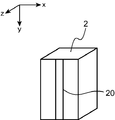
- FIG. 2 is a schematic diagram showing a state in which the laser unit 2 emits the laser beam 10.
- the z direction is the traveling direction of the laser light 10.
- the laser unit 2 is an example of a light source, and is a semiconductor laser including a light emitting unit 20 that emits a pulsed laser beam 10.
- the front surface (that is, the light emitting surface) of the light emitting unit 20 has an elongated rectangular shape with the short side in the x direction and the long side in the y direction. Therefore, when viewed from the traveling direction of the laser beam 10, the laser beam 10 has an elongated shape along the y direction.
- a plurality of single-mode semiconductor lasers or a plurality of fiber lasers may be used to form the laser beam 10 having an elongated rectangular shape with the short side in the x direction and the long side in the y direction.
- the controller 3 controls the entire operation of the laser radar device 1, and includes a CPU (Central Processing Unit), a RAM (Random Access Memory), a ROM (Read Only Memory), and an LD (Laser Diode). Consists of a driver and the like.
- the LD driver is a driver circuit that drives the laser unit 2.
- the controller 3 includes an emission control unit 30 as a functional block.
- the emission control unit 30 repeats the control for causing the laser unit 2 to emit the laser beam 10 periodically (for example, 16.7 ⁇ s).
- the emission of the laser beam 10 is not limited periodically and may be intermittent.
- the collimator lens 4 collimates the laser beam 10 periodically emitted from the laser unit 2 into parallel light.
- the laser beam 10 collimated by the collimator lens 4 is sent to the scanning unit 5.
- the scanning unit 5 is an optical device that scans the laser beam 10 having an elongated shape along the y direction shown in FIG. 2 along the scanning direction.
- the scanning direction is the x direction.
- the scanning unit 5 will be described by taking a polygon mirror 50 and a motor 51 that rotates the polygon mirror 50 as an example.
- the scanning part 5 is not limited to this, A galvanometer mirror, a MEMS mirror, etc. can also be used.
- the motor controller 6 controls the motor 51 and the rotation of the polygon mirror 50 according to the command of the controller 3.
- the laser beam 10 scanned by the polygon mirror 50 is applied to the measurement region R in a state where the cross section has an elongated shape when viewed from the traveling direction of the laser beam 10. Since the laser beam 10 is scanned along the scanning direction (x direction) and the measurement region R is irradiated with the laser beam 10, the measurement region R can be expanded in the scanning direction.
- the reflected light 11 generated when the measurement region R is irradiated with the laser light 10 enters the polygon mirror 50, is reflected by the polygon mirror 50, and is received by the optical system 7.
- the optical system 7 guides the received reflected light 11 to the light receiving unit 8.
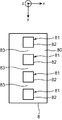
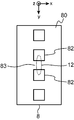
- FIG. 3 is a plan view of the light receiving unit 8.
- the light receiving unit 8 includes a semiconductor substrate and four avalanche photodiodes 81 formed on the semiconductor substrate.
- four avalanche photodiodes 81 will be described as an example, but the number of avalanche photodiodes 81 may be plural.
- Each of the four avalanche photodiodes 81 has a light receiving surface 82 that receives the reflected light 11. Since the four avalanche photodiodes 81 are formed on the semiconductor substrate in a line at a predetermined interval, the four light receiving surfaces 82 are arranged in a line at a predetermined interval. The interval may be constant or may not be constant (for example, the interval may be random).
- the surface 80 of the light receiving unit 8 includes four light receiving surfaces 82 and a region 83 between adjacent light receiving surfaces 82. The light receiving unit 8 is arranged with the direction in which the light receiving surfaces 82 are arranged in the y direction (the direction in which the elongated shape of the reflected light 11 extends).
- FIG. 4 is a perspective view showing an appearance of the laser radar device 1 according to the present embodiment.
- the laser radar device 1 includes a housing 9 that houses the laser unit 2, the controller 3, the collimator lens 4, the scanning unit 5, the motor controller 6, the optical system 7, and the light receiving unit 8 shown in FIG.
- the housing 9 includes a bottomed semicylindrical lower member 90 and a lidded semiconical upper member 91 connected to the upper portion of the lower member 90. A side surface of the upper member 91 having an obliquely curved surface is opened, and a window 92 is provided in the opening.
- FIG. 5 is an explanatory diagram for explaining a state in which the laser beam 10 from the laser radar device 1 irradiates the measurement region R.
- FIG. The reflected light 11 reflected by the measurement region R passes through the window portion 92 and is received by the light receiving portion 8 via the polygon mirror 50 and the optical system 7.
- the optical system 7 when the direction orthogonal to both the direction in which the light receiving surfaces 82 are arranged (y direction) and the traveling direction of the reflected light 11 (z direction) is an orthogonal direction (x direction), the optical system 7 is The reflected light 11 is guided to the light receiving unit 8 with the focal position in the direction in which the light receiving surfaces 82 are aligned aligned with the front or back of the surface 80 of the light receiving unit 8 and with the focal position in the orthogonal direction aligned with the surface 80. This will be described in comparison with the first comparative example and the second comparative example.
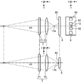
- FIG. 6 is an optical path diagram showing that the reflected light 11 is guided to the light receiving unit 8 through the optical system 7 in the first comparative example.
- the reflected light 11 is the laser light 10 reflected by the measurement region R shown in FIG.
- the reflected light 11 enters the polygon mirror 50 shown in FIG. 1, is reflected by the polygon mirror 50, and is sent to the optical system 7.
- AX indicates the optical axis.
- the optical system 7 of the first comparative example is a light receiving lens.
- the light receiving lens aligns the focal position 13 a in the y direction and the focal position 13 b in the x direction with the surface 80 of the light receiving unit 8. For this reason, since the diameter of the light beam 12 is reduced on the surface 80, the light beam 12 positioned in the region 83 between the adjacent light receiving surfaces 82 cannot be received by the light receiving surface 82.
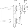
- FIG. 7 is an optical path diagram showing that the reflected light 11 is guided to the light receiving unit 8 through the optical system 7 in the second comparative example.
- the optical system 7 of the second comparative example is a light receiving lens.
- the light receiving lens aligns the focal position 13 a in the y direction and the focal position 13 b in the x direction in front of the surface 80 of the light receiving unit 8. Thereby, since the diameter of the light beam 12 is increased on the surface 80, the light beam 12 positioned in the region 83 between the adjacent light receiving surfaces 82 can reach the light receiving surface 82.
- the focal positions 13a and 13b move in front of (or behind) the surface 80 of the light receiving unit 8 as viewed from the traveling direction of the reflected light 11, that is, when defocused, the light enters the surface 80.
- the diameter of the light beam 12 of the reflected light 11 is increased.
- the light beam 12 of the reflected light 11 located in the region 83 between the adjacent light receiving surfaces 82 can reach the light receiving surface 82, and the light beam 12 can be detected by the light receiving surface 82.
- FIG. 8 is an optical path diagram showing that the reflected light 11 is guided to the light receiving unit 8 through the optical system 7 in the present embodiment.
- the optical system 7 aligns the focal position 13a in the y direction (the direction in which the light receiving surfaces 82 are arranged) with the front (or the rear) of the surface 80 of the light receiving unit 8, and sets the focal position 13b in the x direction (orthogonal direction) to the light receiving unit.
- 8 has a function of guiding the reflected light 11 to the light receiving unit 8 according to the surface 80 of the light.
- the size in the y direction can be made larger than the size in the x direction with respect to the light beam 12 of the reflected light 11 on the surface 80 of the light receiving unit 8 (in other words, the light beam 12 of the reflected light 11 is longer in the y direction). It can be an ellipse with an axis and a minor axis in the x direction).
- the focal position 13a in the y direction is aligned with the front (or the back) of the surface 80 of the light receiving unit 8, so that the reflected light 11 on the surface 80 of the light receiving unit 8 is reflected.
- the size of the light beam 12 in the y direction can be increased.
- the focal position 13b in the x direction is aligned with the surface 80 of the light receiving unit 8, the size of the light beam 12 of the reflected light 11 on the surface 80 of the light receiving unit 8 can be prevented from being increased. .
- the light beam 12 of the reflected light 11 on the surface 80 of the light receiving unit 8 has a large size in the y direction.
- the light beam 12 located in the region 83 can reach the light receiving surface 82.
- the light beam 12 exceeds the light receiving surface 82 in the x direction. If the light receiving surface 82 is enlarged, the light beam 12 can be received by the light receiving surface 82 without exceeding the light receiving surface 82. However, by increasing the light receiving surface 82, the light receiving field is widened, so that noise increases, and as a result, the S / N ratio decreases. Therefore, on the surface 80 of the light receiving unit 8, the luminous flux 12 of the reflected light 11 is not increased in size in the x direction.
- the light receiving unit 8 having a plurality of avalanche photodiodes 81 and having a structure in which the light receiving surfaces 82 of the avalanche photodiodes 81 are arranged in a row at a predetermined interval.
- the ability to receive the reflected light 11 can be improved without reducing the interval between the matching light receiving surfaces 82.
- FIG. 9 is an optical path diagram showing that the reflected light 11 is guided to the light receiving unit 8 through the optical system 7 in the first mode of the optical system 7 provided in the present embodiment.
- the optical system 7 includes a light receiving lens 70 and an optical element 71.
- the light receiving lens 70 is a circular lens that receives the reflected light 11 and focuses it on the light receiving unit 8.
- the light receiving lens 70 aligns the focal position 13 a in the y direction and the focal position 13 b in the x direction with the surface 80 of the light receiving unit 8, receives the reflected light 11, and guides it to the light receiving unit 8.
- the optical element 71 is disposed in front of the light receiving lens 70 when viewed from the z direction (the traveling direction of the reflected light 11), transmits the reflected light 11, and has positive power (also referred to as optical power) only in the y direction.
- Positive power also referred to as optical power
- Have. Power is the reciprocal of the focal length.
- the optical element 71 is, for example, a cylinder lens or a diffraction grating.
- the optical element 71 may be disposed behind the light receiving lens 70. About these, it can say also about a 2nd aspect, a 3rd aspect, and a 4th aspect.
- the optical element 71 provided in the first aspect of the optical system 7 transmits the reflected light 11 and has a positive power only in the y direction. Accordingly, the focal position 13a in the y direction of the optical system 7 is moved from the surface 80 of the light receiving section 8 to the front of the surface 80 in a state where the focal position 13b in the x direction of the optical system 7 is aligned with the surface 80 of the light receiving section 8. (In other words, only the y direction is defocused and the x direction is not defocused).
- FIG. 10 is an optical path diagram showing that the reflected light 11 is guided to the light receiving unit 8 through the optical system 7 in the second mode of the optical system 7 provided in the present embodiment.
- the optical system 7 includes a light receiving lens 70 and an optical element 71.
- the second aspect is different from the first aspect as follows. In the first aspect, an optical element 71 that transmits the reflected light 11 and has a positive power only in the y direction is used. On the other hand, in the second mode, an optical element 71 that transmits the reflected light 11 and has negative power only in the y direction is used.
- the optical element 71 provided in the second aspect of the optical system 7 transmits the reflected light 11 and has negative power only in the y direction. Accordingly, the focal position 13a in the y direction of the optical system 7 is moved from the surface 80 of the light receiving section 8 to the rear of the surface 80 in a state where the focal position 13b in the x direction of the optical system 7 is aligned with the surface 80 of the light receiving section 8. (In other words, only the y direction is defocused and the x direction is not defocused).
- FIG. 11 is an optical path diagram showing that the reflected light 11 is guided to the light receiving unit 8 through the optical system 7 in the third mode of the optical system 7 provided in the present embodiment.
- the optical system 7 includes a light receiving lens 70 and an optical element 71.
- the light receiving lens 70 is a circular lens that receives the reflected light 11 and focuses it on the light receiving unit 8.
- the light receiving lens 70 aligns the focal position 13 a in the y direction and the focal position 13 b in the x direction behind the surface 80 of the light receiving unit 8, receives the reflected light 11, and guides it to the light receiving unit 8.
- the optical element 71 is disposed in front of the light receiving lens 70 when viewed from the z direction (the traveling direction of the reflected light 11), transmits the reflected light 11, and has a positive power only in the x direction.
- the optical element 71 provided in the third aspect of the optical system 7 transmits the reflected light 11 and has a positive power only in the x direction.
- the focal position 13b in the x direction of the optical system 7 is aligned from the rear side of the surface 80 of the light receiving unit 8 with the focal position 13a in the y direction of the optical system 7 aligned with the rear side of the surface 80 of the light receiving unit 8. (In other words, only the y direction is defocused and the x direction is not defocused).
- FIG. 12 is an optical path diagram showing that the reflected light 11 is guided to the light receiving unit 8 through the optical system 7 in the fourth aspect of the optical system 7 provided in the present embodiment.
- the optical system 7 includes a light receiving lens 70 and an optical element 71.
- the fourth aspect differs from the third aspect in the following points.
- the light receiving lens 70 that matches the focal position 13a in the y direction and the focal position 13b in the x direction to the front of the surface 80 of the light receiving unit 8 is used.
- the optical element 71 that transmits the reflected light 11 and has negative power only in the x direction is used.
- the optical element 71 provided in the fourth aspect of the optical system 7 transmits the reflected light 11 and has negative power only in the x direction.
- the focal position 13b in the x direction of the optical system 7 is aligned from the front of the surface 80 of the light receiving section 8 to the front surface 80 in a state where the focal position 13a in the y direction of the optical system 7 is aligned with the front of the surface 80 of the light receiving section 8. (In other words, only the y direction is defocused and the x direction is not defocused).
- an anamorphic lens is used as the optical system 7.
- the anamorphic lens is a lens that compresses the light beam 12 only in one direction.
- FIG. 13 shows the luminous flux 12 positioned in the region 83 between the adjacent light receiving surfaces 82 when the focal position of the anamorphic lens (the focal position in the x direction and the focal position in the y direction) is matched with the surface 80 of the light receiving unit 8.
- the shape of the light beam 12 of the reflected light 11 is an elliptical shape having the major axis in the y direction and the minor axis in the x direction.
- FIG. 14 is a schematic diagram showing a light beam 12 positioned in a region 83 between adjacent light receiving surfaces 82 in the optical system 7 provided in the modification of the present embodiment. Since the anamorphic lens has the focal position in the y direction (the direction in which the light receiving surfaces 82 are arranged) aligned with the front or back of the surface 80 of the light receiving unit 8 and the focal position in the x direction (orthogonal direction) aligned with the surface 80. The surface 80 of the light receiving unit 8 is defocused. For this reason, the elliptical luminous flux 12 shown in FIG. 13 is expanded into the elliptical luminous flux 12 shown in FIG.
- the size of the reflected light 11 in the y direction can be increased on the surface 80 of the light receiving unit 8.
- the size of the reflected light 11 in the x direction can be prevented from being increased.
- the light receiving device has a structure in which a plurality of avalanche photodiodes 81 are provided and the light receiving surfaces 82 of the avalanche photodiodes 81 are arranged in a row at a predetermined interval.
- the ability to receive the reflected light 11 can be improved without reducing the interval between the adjacent light receiving surfaces 82.
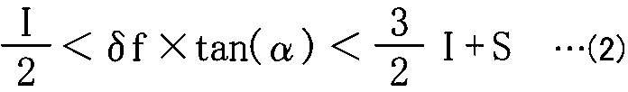
- FIG. 15 is an explanatory diagram illustrating a lower limit value and an upper limit value for the size of the light beam 12 in the y direction.
- the lower limit value and the upper limit value are defined by Expression (1).
- I indicates the interval between adjacent light receiving surfaces 82.
- ⁇ f represents the difference between the back focus bf of the light receiving lens 70 in the y direction (the direction in which the light receiving surfaces 82 are arranged) and the back focus bf of the light receiving lens 70 in the x direction (the orthogonal direction).
- Back focus refers to the distance from the end of the lens system to the focal point.
- ⁇ indicates the opening angle of the light receiving lens 70 in the y direction.
- S indicates the size of the light receiving surface 82 in the y direction.
- ⁇ f ⁇ tan ( ⁇ ) indicates a half value of the size of the light beam 12 in the y direction on the surface 80 of the light receiving unit 8. By making this half value larger than I / 2, the light flux 12 of the reflected light 11 located in the region 83 between the adjacent light receiving surfaces 82 can reach at least one of the light receiving surfaces 82.
- the half value is made smaller than I ⁇ 3/2 + S. Thereby, the light flux 12 of the reflected light 11 positioned in the region 83 between the adjacent light receiving surfaces 82 reaches the light receiving surfaces 82 a and 82 b positioned adjacent to these light receiving surfaces 82 beyond the adjacent light receiving surfaces 82. I can not.
- the half value is I / 2 ⁇ f ⁇ tan ( ⁇ ) ⁇ I / 2 + S
- the luminous flux 12 of the reflected light 11 located in the region 83 between the adjacent light receiving surfaces 82 is adjacent. Since it can prevent exceeding the light-receiving surface 82, the fall of the light quantity which can be received by the light-receiving surface 82 can be suppressed.
- the light receiving lens 70 is read as an anamorphic lens.
- the present invention can be applied to any light projecting / receiving device without being limited to the laser radar device 1.
- the light projecting / receiving device includes a light source that emits light having a long and narrow cross section when viewed from the traveling direction of light, and the measurement region is irradiated with the light emitted from the light source.
- a plurality of avalanche photodiodes having a light receiving surface for receiving reflected light reflected by the measurement region, a structure in which the light receiving surfaces are arranged in a row with a predetermined interval in a direction in which the elongated shape extends, and
- the light receiving surface having a light receiving surface having a surface including a region between the light receiving surface and the adjacent light receiving surface, and a direction orthogonal to both the direction in which the light receiving surfaces are arranged and the traveling direction of the reflected light are orthogonal.
- an optical system that guides the reflected light to the light receiving unit with the focal position in the direction in which the lines are aligned in front of or behind the surface and the focal position in the orthogonal direction is aligned with the surface.
- the optical system has a function of guiding the reflected light to the light receiving unit by aligning the focal position in the direction in which the light receiving surfaces are aligned with the front or back of the surface of the light receiving unit and aligning the focal position in the orthogonal direction with the surface of the light receiving unit.
- the focal position in the direction in which the light receiving surfaces are arranged is aligned with the front or back of the surface of the light receiving unit, so that the size of the reflected light beam on the surface of the light receiving unit is increased in the direction in which the light receiving surfaces are arranged. it can.
- the focal position in the orthogonal direction is aligned with the surface of the light receiving unit, the size of the reflected light beam on the surface of the light receiving unit can be prevented from increasing.
- the reflected light beam on the surface of the light receiving portion has a larger size in the direction in which the light receiving surfaces are arranged, so that the light beam positioned in the region between the adjacent light receiving surfaces is used as the light receiving surface. Can reach.
- the light beam passes the light receiving surface in the orthogonal direction. If the light receiving surface is enlarged, the light beam can be received by the light receiving surface without exceeding the light receiving surface. However, by increasing the light receiving surface, the light receiving field is widened, so that noise increases, and as a result, the S / N ratio decreases. Thus, the light flux of the reflected light on the surface of the light receiving unit is not increased in size in the orthogonal direction.
- the light receiving unit includes a plurality of avalanche photodiodes, and the light receiving surfaces of the avalanche photodiodes are arranged in a row at a predetermined interval.
- the ability to receive reflected light can be improved without reducing the interval between adjacent light receiving surfaces.
- the optical system has a light receiving lens that receives the reflected light and guides the reflected light to the light receiving unit, in which the light receiving surface is aligned and the focal position in the orthogonal direction is aligned with the surface, and the reflected light And an optical element that is disposed in front of or behind the light receiving lens and has a positive or negative power only in a direction in which the light receiving surfaces are arranged.
- This configuration includes the first and second aspects of the optical system.
- the optical element provided in the first aspect transmits reflected light and has a positive power only in the direction in which the light receiving surfaces are arranged.
- the focal position in the direction in which the light receiving surfaces of the optical system are arranged can be moved from the surface of the light receiving section to the front of the surface in a state where the orthogonal position of the optical system is aligned with the surface of the light receiving section.
- the optical element provided in the second aspect transmits reflected light and has negative power only in the direction in which the light receiving surfaces are arranged.
- the focal position in the direction in which the light receiving surfaces of the optical system are arranged can be moved from the surface of the light receiving section to the rear of the surface in a state in which the focal position in the orthogonal direction of the optical system is aligned with the surface of the light receiving section.
- the optical system has a light receiving lens in which the light receiving surface is aligned and the focal position in the orthogonal direction is adjusted to the rear of the surface, and the reflected light is received and guided to the light receiving unit;
- An optical element that is disposed in front of or behind the light receiving lens when viewed from the traveling direction of the reflected light and has a positive power only in the orthogonal direction with respect to the reflected light.
- This configuration is the third aspect of the optical system.
- the focal position in the orthogonal direction of the optical system is moved from the rear of the surface of the light receiving section to this surface in a state where the focal position in the direction in which the light receiving surfaces of the optical system are aligned is aligned with the rear of the surface of the light receiving section. Can do.
- the optical system has a light receiving lens in which the light receiving surface is aligned and the focal position in the orthogonal direction is aligned with the front of the surface, and the reflected light is received and guided to the light receiving unit; And an optical element that is disposed in front of or behind the light receiving lens as viewed from the traveling direction of the reflected light and has a negative power only in the orthogonal direction with respect to the reflected light.
- This configuration is the fourth aspect of the optical system.
- the focal position in the orthogonal direction of the optical system is moved from the front of the surface of the light receiving section to this surface. Can do.
- the optical system includes an anamorphic lens that guides the reflected light to the light receiving unit with a focal position in front of or behind the surface, and with the orthogonal focal position on the surface.
- the functions of the optical system described above can be realized with a single optical element.
- the optical system satisfies the following formula (1).
- I indicates the interval between the adjacent light receiving surfaces
- ⁇ f indicates the difference between the back focus of the light receiving lens in the direction in which the light receiving surfaces are aligned and the back focus of the light receiving lens in the orthogonal direction
- ⁇ represents the aperture angle of the light receiving lens in the direction in which the light receiving surfaces are arranged
- S represents the size of the light receiving surface in the direction in which the light receiving surfaces are arranged.
- the optical system increases the size of the reflected light beam on the surface of the light receiving unit in the direction in which the light receiving surfaces are arranged.
- ⁇ f ⁇ tan ( ⁇ ) indicates a half value of the size of the light beam in the direction in which the light receiving surfaces are arranged on the surface of the light receiving unit. By making this half value larger than I / 2, the light flux of reflected light positioned between adjacent light receiving surfaces can reach at least one light receiving surface.
- the half value is made smaller than I ⁇ 3/2 + S.
- the optical system satisfies the following formula (2).
- I indicates the interval between the adjacent light receiving surfaces
- ⁇ f indicates the difference between the back focus of the anamorphic lens in the direction in which the light receiving surfaces are aligned and the back focus of the anamorphic lens in the orthogonal direction
- ⁇ represents the opening angle of the anamorphic lens in the direction in which the light receiving surfaces are arranged
- S represents the size of the light receiving surface in the direction in which the light receiving surfaces are arranged.
- Another aspect of the embodiment is a laser radar device including the light projecting and receiving device according to one aspect of the embodiment, wherein the light source includes the laser light having a long and narrow cross section when viewed from the traveling direction of the laser light.
- the light a laser unit that emits light is provided, and the laser radar device includes a scanning unit that scans the laser light emitted by the laser unit along a scanning direction and irradiates the scanned laser light on the measurement region.
- the laser beam is scanned along the scanning direction and the measurement region is irradiated with the laser beam, so that the measurement region can be expanded in the scanning direction.
Landscapes
- Engineering & Computer Science (AREA)
- Physics & Mathematics (AREA)
- Computer Networks & Wireless Communication (AREA)
- General Physics & Mathematics (AREA)
- Radar, Positioning & Navigation (AREA)
- Remote Sensing (AREA)
- Electromagnetism (AREA)
- Optical Radar Systems And Details Thereof (AREA)
Abstract
Description

実施形態の一局面に係る投受光装置は、光の進行方向から見て断面が細長形状を有する光を出射する光源と、前記光源から出射された光が測定領域に照射されることにより、前記測定領域で反射された反射光を受光する受光面を有するアバランシェフォトダイオードを複数備え、前記細長形状が延びる方向に所定の間隔を設けて、前記受光面が一列に並べられた構造、並びに、前記受光面及び隣り合う前記受光面の間の領域を含む表面を有する受光部と、前記受光面が並ぶ方向及び前記反射光の進行方向の両方と直交する方向を直交方向としたとき、前記受光面が並ぶ方向の焦点位置を前記表面の前方又は後方に合わせ、かつ、前記直交方向の焦点位置を前記表面に合わせて、前記反射光を前記受光部に導く光学系と、を備える。

Claims (8)
- 光の進行方向から見て断面が細長形状を有する光を出射する光源と、
前記光源から出射された光が測定領域に照射されることにより、前記測定領域で反射された反射光を受光する受光面を有するアバランシェフォトダイオードを複数備え、前記細長形状が延びる方向に所定の間隔を設けて、前記受光面が一列に並べられた構造、並びに、前記受光面及び隣り合う前記受光面の間の領域を含む表面を有する受光部と、
前記受光面が並ぶ方向及び前記反射光の進行方向の両方と直交する方向を直交方向としたとき、前記受光面が並ぶ方向の焦点位置を前記表面の前方又は後方に合わせ、かつ、前記直交方向の焦点位置を前記表面に合わせて、前記反射光を前記受光部に導く光学系と、を備える投受光装置。 - 前記光学系は、
前記受光面が並ぶ方向及び前記直交方向の焦点位置を、前記表面に合わせており、前記反射光を受光して前記受光部に導く受光レンズと、
前記反射光の進行方向から見て、前記受光レンズの前方又は後方に配置され、前記反射光を透過させ、前記受光面が並ぶ方向にのみ正又は負のパワーを有する光学素子と、を備える請求項1に記載の投受光装置。 - 前記光学系は、
前記受光面が並ぶ方向及び前記直交方向の焦点位置を、前記表面の後方に合わせており、前記反射光を受光して前記受光部に導く受光レンズと、
前記反射光の進行方向から見て、前記受光レンズの前方又は後方に配置され、前記反射光を透過させ、前記直交方向にのみ正のパワーを有する光学素子と、を備える請求項1に記載の投受光装置。 - 前記光学系は、
前記受光面が並ぶ方向及び前記直交方向の焦点位置を、前記表面の前方に合わせており、前記反射光を受光して前記受光部に導く受光レンズと、
前記反射光の進行方向から見て、前記受光レンズの前方又は後方に配置され、前記反射光を透過させ、前記直交方向にのみ負のパワーを有する光学素子と、を備える請求項1に記載の投受光装置。 - 前記光学系は、前記表面の前方又は後方に焦点位置を合わせ、かつ、前記直交方向の焦点位置を前記表面に合わせて、前記反射光を前記受光部に導くアナモフィックレンズを備える請求項1に記載の投受光装置。
- 前記光学系は、下記式(1)を満たす請求項2~4のいずれか一項に記載の投受光装置。

- 前記光学系は、下記式(2)を満たす請求項5に記載の投受光装置。

- 請求項1~7のいずれか一項に記載の投受光装置を備えるレーザーレーダー装置であって、
前記光源は、レーザー光の進行方向から見て、断面が細長形状を有する前記レーザー光を前記光として、出射するレーザー部を備え、
前記レーザーレーダー装置は、
前記レーザー部が出射した前記レーザー光を走査方向に沿って走査し、走査したレーザー光を前記測定領域に照射する走査部を備えるレーザーレーダー装置。
Priority Applications (3)
| Application Number | Priority Date | Filing Date | Title |
|---|---|---|---|
| JP2017531114A JP6575596B2 (ja) | 2015-07-24 | 2016-07-07 | 投受光装置及びこれを備えるレーザーレーダー装置 |
| US15/745,943 US10802115B2 (en) | 2015-07-24 | 2016-07-07 | Light projecting and receiving device, and laser radar device provided with same |
| EP16830257.8A EP3312628A4 (en) | 2015-07-24 | 2016-07-07 | Light projecting and receiving device, and laser radar device provided with same |
Applications Claiming Priority (2)
| Application Number | Priority Date | Filing Date | Title |
|---|---|---|---|
| JP2015-146987 | 2015-07-24 | ||
| JP2015146987 | 2015-07-24 |
Publications (1)
| Publication Number | Publication Date |
|---|---|
| WO2017018152A1 true WO2017018152A1 (ja) | 2017-02-02 |
Family
ID=57885183
Family Applications (1)
| Application Number | Title | Priority Date | Filing Date |
|---|---|---|---|
| PCT/JP2016/070099 WO2017018152A1 (ja) | 2015-07-24 | 2016-07-07 | 投受光装置及びこれを備えるレーザーレーダー装置 |
Country Status (4)
| Country | Link |
|---|---|
| US (1) | US10802115B2 (ja) |
| EP (1) | EP3312628A4 (ja) |
| JP (1) | JP6575596B2 (ja) |
| WO (1) | WO2017018152A1 (ja) |
Cited By (3)
| Publication number | Priority date | Publication date | Assignee | Title |
|---|---|---|---|---|
| JP2018132524A (ja) * | 2017-02-14 | 2018-08-23 | バイドゥ・ユーエスエイ・リミテッド・ライアビリティ・カンパニーBaidu USA LLC | Lidar装置及びlidar装置を操作するための方法 |
| WO2018206422A1 (de) * | 2017-05-11 | 2018-11-15 | Robert Bosch Gmbh | Laserscanner für ein lidar-system und verfahren zum betreiben eines laserscanners |
| US11550038B2 (en) * | 2018-09-26 | 2023-01-10 | Apple Inc. | LIDAR system with anamorphic objective lens |
Families Citing this family (3)
| Publication number | Priority date | Publication date | Assignee | Title |
|---|---|---|---|---|
| US10955531B2 (en) | 2017-06-21 | 2021-03-23 | Apple Inc. | Focal region optical elements for high-performance optical scanners |
| US10775485B2 (en) * | 2017-10-20 | 2020-09-15 | Korea Electronics Technology Institute | LIDAR device and system comprising the same |
| JP7113669B2 (ja) * | 2018-06-08 | 2022-08-05 | 株式会社クボタ | 作業車に搭載されるレーザレーダ |
Citations (3)
| Publication number | Priority date | Publication date | Assignee | Title |
|---|---|---|---|---|
| JP2000180133A (ja) * | 1998-12-10 | 2000-06-30 | Toshiba Corp | 形状検知装置 |
| JP2008076390A (ja) * | 2006-09-15 | 2008-04-03 | Triple-In Holding Ag | 距離撮像 |
| JP2008256539A (ja) * | 2007-04-05 | 2008-10-23 | Konica Minolta Holdings Inc | 光学的測定装置及び光学的測定方法 |
Family Cites Families (9)
| Publication number | Priority date | Publication date | Assignee | Title |
|---|---|---|---|---|
| SE407976B (sv) * | 1973-03-13 | 1979-04-30 | Bofors Ab | Forfarande och anordning for malfoljning |
| DE3412076A1 (de) | 1984-03-31 | 1985-10-03 | Isco-Optic GmbH, 3400 Göttingen | Vorrichtung zur zweidimensionalen vermessung von lichtpunkten |
| US4916536A (en) * | 1988-11-07 | 1990-04-10 | Flir Systems, Inc. | Imaging range finder and method |
| JP3288523B2 (ja) * | 1994-02-22 | 2002-06-04 | 株式会社ワコム | 光点位置計測装置及び光点位置計測方法 |
| JPH1164518A (ja) * | 1997-08-12 | 1999-03-05 | Mitsubishi Electric Corp | 車両用光レーダ装置 |
| DE202006005876U1 (de) * | 2006-04-11 | 2007-08-16 | Leuze Electronic Gmbh & Co Kg | Optischer Sensor |
| JP5177003B2 (ja) | 2009-02-19 | 2013-04-03 | 株式会社デンソーウェーブ | レーザ距離測定装置 |
| LU91714B1 (en) * | 2010-07-29 | 2012-01-30 | Iee Sarl | Active illumination scanning imager |
| NO335488B1 (no) * | 2013-03-22 | 2014-12-22 | Kongsberg Seatex As | Posisjonsreferansesystem og fremgangsmåte for posisjonering og sporing av ett eller flere objekter |
-
2016
- 2016-07-07 EP EP16830257.8A patent/EP3312628A4/en active Pending
- 2016-07-07 JP JP2017531114A patent/JP6575596B2/ja active Active
- 2016-07-07 WO PCT/JP2016/070099 patent/WO2017018152A1/ja active Application Filing
- 2016-07-07 US US15/745,943 patent/US10802115B2/en active Active
Patent Citations (3)
| Publication number | Priority date | Publication date | Assignee | Title |
|---|---|---|---|---|
| JP2000180133A (ja) * | 1998-12-10 | 2000-06-30 | Toshiba Corp | 形状検知装置 |
| JP2008076390A (ja) * | 2006-09-15 | 2008-04-03 | Triple-In Holding Ag | 距離撮像 |
| JP2008256539A (ja) * | 2007-04-05 | 2008-10-23 | Konica Minolta Holdings Inc | 光学的測定装置及び光学的測定方法 |
Non-Patent Citations (1)
| Title |
|---|
| See also references of EP3312628A4 * |
Cited By (5)
| Publication number | Priority date | Publication date | Assignee | Title |
|---|---|---|---|---|
| JP2018132524A (ja) * | 2017-02-14 | 2018-08-23 | バイドゥ・ユーエスエイ・リミテッド・ライアビリティ・カンパニーBaidu USA LLC | Lidar装置及びlidar装置を操作するための方法 |
| US10976413B2 (en) | 2017-02-14 | 2021-04-13 | Baidu Usa Llc | LIDAR system with synchronized MEMS mirrors |
| WO2018206422A1 (de) * | 2017-05-11 | 2018-11-15 | Robert Bosch Gmbh | Laserscanner für ein lidar-system und verfahren zum betreiben eines laserscanners |
| US11561302B2 (en) | 2017-05-11 | 2023-01-24 | Robert Bosch Gmbh | Laser scanner for a LIDAR system and method for operating a laser scanner |
| US11550038B2 (en) * | 2018-09-26 | 2023-01-10 | Apple Inc. | LIDAR system with anamorphic objective lens |
Also Published As
| Publication number | Publication date |
|---|---|
| US20180224530A1 (en) | 2018-08-09 |
| US10802115B2 (en) | 2020-10-13 |
| JPWO2017018152A1 (ja) | 2018-05-10 |
| EP3312628A4 (en) | 2018-08-15 |
| EP3312628A1 (en) | 2018-04-25 |
| JP6575596B2 (ja) | 2019-09-18 |
Similar Documents
| Publication | Publication Date | Title |
|---|---|---|
| JP6575596B2 (ja) | 投受光装置及びこれを備えるレーザーレーダー装置 | |
| US9568358B2 (en) | Optical measurement device and vehicle | |
| US9285266B2 (en) | Object detector including a light source with light emitting region of a first size in a first direction and a second size in a second direction | |
| US11119194B2 (en) | Laser radar device | |
| EP2940489B1 (en) | Object detection device and sensing apparatus | |
| KR102020037B1 (ko) | 하이브리드 라이다 스캐너 | |
| US11585902B2 (en) | Optical designs using cylindrical lenses for improved resolution in lidar systems | |
| KR102210101B1 (ko) | 광학계 모듈 및 그를 갖는 스캐닝 라이다 | |
| JP6737296B2 (ja) | 対象物検出装置 | |
| CN111656215A (zh) | 激光雷达装置、驾驶辅助系统以及车辆 | |
| CN111670377A (zh) | 激光雷达装置 | |
| JP2014059222A (ja) | 光レーダ装置 | |
| US10162171B2 (en) | Scanning optical system and light projecting and receiving apparatus | |
| JP2018100880A (ja) | 物体検出装置 | |
| JP6594282B2 (ja) | レーザレーダ装置 | |
| JP2018151286A (ja) | 物体検出装置 | |
| JP7473067B2 (ja) | 光走査装置、物体検出装置及びセンシング装置 | |
| US20230305113A1 (en) | Light detection device | |
| EP3761056B1 (en) | Optical scanner, object detector, and sensing apparatus | |
| WO2017130729A1 (ja) | レーザレーダ装置 | |
| JP2017125765A (ja) | 対象物検出装置 | |
| JP6663156B2 (ja) | 物体検出装置 | |
| CN111656214A (zh) | 光学雷达装置 | |
| JP2023073072A (ja) | 光学装置 | |
| US20190196016A1 (en) | Asymmetric optical sensor device |
Legal Events
| Date | Code | Title | Description |
|---|---|---|---|
| 121 | Ep: the epo has been informed by wipo that ep was designated in this application |
Ref document number: 16830257 Country of ref document: EP Kind code of ref document: A1 |
|
| ENP | Entry into the national phase |
Ref document number: 2017531114 Country of ref document: JP Kind code of ref document: A |
|
| WWE | Wipo information: entry into national phase |
Ref document number: 15745943 Country of ref document: US |
|
| NENP | Non-entry into the national phase |
Ref country code: DE |
|
| WWE | Wipo information: entry into national phase |
Ref document number: 2016830257 Country of ref document: EP |