WO2017006728A1 - 巻回型フィルムコンデンサ - Google Patents
巻回型フィルムコンデンサ Download PDFInfo
- Publication number
- WO2017006728A1 WO2017006728A1 PCT/JP2016/067861 JP2016067861W WO2017006728A1 WO 2017006728 A1 WO2017006728 A1 WO 2017006728A1 JP 2016067861 W JP2016067861 W JP 2016067861W WO 2017006728 A1 WO2017006728 A1 WO 2017006728A1
- Authority
- WO
- WIPO (PCT)
- Prior art keywords
- film
- wound
- glass
- width direction
- conductive layer
- Prior art date
- Legal status (The legal status is an assumption and is not a legal conclusion. Google has not performed a legal analysis and makes no representation as to the accuracy of the status listed.)
- Ceased
Links
Images



Classifications
-
- H—ELECTRICITY
- H01—ELECTRIC ELEMENTS
- H01G—CAPACITORS; CAPACITORS, RECTIFIERS, DETECTORS, SWITCHING DEVICES, LIGHT-SENSITIVE OR TEMPERATURE-SENSITIVE DEVICES OF THE ELECTROLYTIC TYPE
- H01G4/00—Fixed capacitors; Processes of their manufacture
- H01G4/002—Details
- H01G4/018—Dielectrics
- H01G4/06—Solid dielectrics
- H01G4/08—Inorganic dielectrics
-
- H—ELECTRICITY
- H01—ELECTRIC ELEMENTS
- H01G—CAPACITORS; CAPACITORS, RECTIFIERS, DETECTORS, SWITCHING DEVICES, LIGHT-SENSITIVE OR TEMPERATURE-SENSITIVE DEVICES OF THE ELECTROLYTIC TYPE
- H01G4/00—Fixed capacitors; Processes of their manufacture
- H01G4/002—Details
- H01G4/018—Dielectrics
- H01G4/06—Solid dielectrics
- H01G4/14—Organic dielectrics
- H01G4/18—Organic dielectrics of synthetic material, e.g. derivatives of cellulose
-
- H—ELECTRICITY
- H01—ELECTRIC ELEMENTS
- H01G—CAPACITORS; CAPACITORS, RECTIFIERS, DETECTORS, SWITCHING DEVICES, LIGHT-SENSITIVE OR TEMPERATURE-SENSITIVE DEVICES OF THE ELECTROLYTIC TYPE
- H01G4/00—Fixed capacitors; Processes of their manufacture
- H01G4/32—Wound capacitors
Definitions
- the present invention relates to a wound film capacitor, and more specifically, relates to a wound film capacitor in which a glass film as an insulating film is wound.
- an inverter In an electric vehicle (EV) and a hybrid electric vehicle (HEV), an inverter is used to drive the AC motor by converting the DC power of the battery into AC power.
- a DC power supply circuit (converter, battery, etc.) connected to the inverter switching circuit is generally called a DC link, and the DC power supply voltage is called a DC link voltage.
- a large-capacitance capacitor called a DC link capacitor is connected in parallel with the DC power source in the DC link of the inverter, and these capacitors compensate for instantaneous load fluctuations caused by the switching circuit.
- Capacitors used for this purpose are required to have the following characteristics. (1) A large amount of energy can be released / stored instantaneously to compensate for instantaneous load fluctuations, and (2) the temperature dependence of the dielectric constant to prevent the circuit from operating properly due to temperature changes. The nature is small.
- ceramic capacitors using BaTiO 3 are mainly used as capacitors for this purpose.
- this ceramic capacitor has a problem that dielectric breakdown occurs when a high voltage is applied. The reason is that when the convex portions of the crystal grains present in the ceramic capacitor are in contact with the electrode and a high voltage is applied to the contact portion, electric field concentration occurs and a short circuit is likely to occur.
- a ceramic capacitor using BaTiO 3 has a large temperature dependence of dielectric constant, and the dielectric constant is likely to change due to temperature change. Therefore, in order to reduce the temperature dependence of the dielectric constant, it has been considered to be doped with Mg or Mn or the like during BaTiO 3.
- Mg, Mn, or the like when Mg, Mn, or the like is doped, a relative charge of ⁇ 2 is induced in the crystal lattice of BaTiO 3 . This may cause oxygen defects in BaTiO 3 . This oxygen defect may cause a decrease in dielectric constant under a DC voltage. Therefore, in a ceramic capacitor using BaTiO 3 , it is difficult to reduce the temperature dependence of the dielectric constant while increasing the dielectric constant.
- the present invention should solve the problem of improving the capacitance per unit volume and providing a capacitor that can exhibit a high dielectric constant without being affected by the ambient temperature at low cost.
- the wound film capacitor according to the present invention. That is, in this capacitor, the first and second conductive layers and the first and second insulating films are the first conductive layer, the first insulating film, the second conductive layer, and the second insulating film.
- the wound film capacitor is provided with a wound body that is wound into a roll shape in the state of being overlapped in the above order, and is characterized in that at least the first insulating film is a glass film.
- the first and second insulating films and the first and second conductive layers are alternately wound in a roll shape with the first and second conductive layers overlapping each other.
- at least the first insulating film was a glass film. Since glass is unlikely to generate oxygen vacancies, the temperature dependence of the dielectric constant can be reduced without reducing the dielectric constant. Therefore, by configuring the capacitor with a wound body in the form of a roll of a film made of glass and a conductive layer, while increasing the capacitance per unit volume of the capacitor, due to temperature changes, The situation where the circuit does not operate properly can be effectively prevented. Therefore, a capacitor capable of storing a large amount of energy and excellent in high temperature environmental characteristics can be manufactured in a relatively small size.
- the second insulating film is a glass film
- the first and second conductive layers are both metal films
- the first glass film has one thickness direction.
- a first surface oriented and a second surface oriented in the other thickness direction, the first metal film is formed on the first surface
- the second glass film is one in the thickness direction.
- a fourth surface directed to the other in the thickness direction, and a second metal film may be formed on the third surface.
- the first glass film and the second glass film are overlapped and wound so that the first metal film and the second metal film do not come into contact with each other. can do.
- the bending stress of the glass film may be excessive, leading to damage.
- one metal film is integrally formed on one glass film and wound together, compared to the case where a metal film is formed on each of the first and second surfaces. Since the bending stress of the glass film is reduced, the probability of breakage can be kept low, and stable production becomes possible.
- the second insulating film is a resin film
- the first and second conductive layers are both metal films
- the thickness dimension of the glass film is 50 ⁇ m or less
- the glass film has a first surface and a second surface oriented in opposite directions in the thickness direction, a first metal film is formed on the first surface, and a second surface is formed on the second surface.
- a metal film may be formed.
- the thickness dimension of the glass film As described above, by setting the thickness dimension of the glass film to 50 ⁇ m or less, the surface area per unit volume (area of the first and second surfaces) increases, so that it is easy to store a large amount of energy. Moreover, since the flexibility improves as the glass film becomes thinner (at 50 ⁇ m or less), the minimum radius of curvature of the glass film can be reduced. Therefore, it is easy to reduce the size of the capacitor.
- the glass film by winding the glass film on the resin film and forming a wound body, it is possible to effectively avoid contact between the metal films. Furthermore, according to this structure, since the bending stress of the glass film produced when winding up a glass film is relieved with a resin film, the failure probability of a glass film can be reduced. In addition, even when the glass film in a state where the metal film is formed on the first and second surfaces and the glass film alone having no metal film on the first and second surfaces are overlapped and wound, although it is possible to avoid contact between the films, depending on the winding condition, the bending stress of the glass film may be excessive, leading to damage.
- the glass film when a single glass film having no metal film is used as a resin film, the glass film has a metal film as well as a case where a glass film having a metal film is wound to form a wound body. Bending stress is reduced. Therefore, the probability that the glass film is damaged can be kept low, and stable production is possible.
- the second insulating film may be a glass film, and both the first and second conductive layers may be metal films.
- the two metal films and the two glass films are wound in a state where the first metal film, the first glass film, the second metal film, and the second glass film are overlapped in this order.
- contact between the metal films can be effectively avoided.
- the bending stress of the glass film which arises at the time of winding can be relieve
- the wound film capacitor according to the present invention includes a first side end face in which the first conductive layer is oriented in one width direction of the wound body, and a second side in which the other width direction of the wound body is oriented.
- the second conductive layer has a third end surface that faces one side in the width direction, and a fourth end surface that faces the other side in the width direction, and the second side end surface is the fourth side end surface.
- the third side end face may be offset to the other side in the width direction than the first side end face.
- the width direction of a wound body here shall mean the direction orthogonal to both the longitudinal direction of the insulating film in the state which comprised the wound body, and the thickness direction (it is the same in this specification hereafter).
- the conductive layer (metal film) on the side to be connected can be easily identified. Further, it is possible to reliably avoid contact with the conductive layer on the side that should not be connected, and to easily and safely perform electrical connection between each electrode and the conductive layer on the side that should be connected to each electrode.
- the wound film capacitor according to the present invention is such that the first glass film is oriented in one width direction of the wound body.
- the second glass film has one side end face and a second side end face that faces the other in the width direction of the wound body, and the second glass film points to the other side in the width direction.
- the first metal film is offset to one side in the width direction from the second side end face and the fourth side end face, and the second metal film is the first side end face. It may be offset to the other side in the width direction from the side end surface and the third side end surface.
- the metal film (conductive layer) on the side to be connected can be easily identified. Further, it is possible to reliably avoid contact with the metal film on the side that should not be connected, and to easily and safely perform electrical connection between each electrode and the metal film on the side that should be connected to each electrode.
- the first electrode that is in contact with the first conductive layer and separated from the second conductive layer is formed on one side in the width direction of the wound body.
- a second electrode that is in contact with the second conductive layer and is separated from the first conductive layer may be formed on the other side in the width direction of the wound body.
- each conductive layer is arranged in an offset (shifted) direction different from each other in the width direction of the wound body, so that the gap between the electrode and the conductive layer on the non-connecting side that does not correspond to this electrode.
- a state having a predetermined gap in the width direction Therefore, it is possible to easily form a state in which only the conductive layer on the side to be connected is in contact with, without particularly making the electrode in a complicated shape (such as a partially protruding shape).
- the action as an inductor is suppressed, and thus it becomes easy to suppress resistance particularly in a high frequency region.
- the wound film capacitor according to the present invention is the first The metal film protrudes from the first and third side end faces to one side in the width direction of the wound body, and the first protrusion is bent and adjacent in the radial direction of the wound body.
- the second metal film is in contact with the first metal film and protrudes to the other side in the width direction of the wound body from the second and fourth side end faces.
- the part may be bent and in contact with the second metal film adjacent in the radial direction of the wound body.
- the protruding portion from the glass film of each metal film is bent to be in contact with the adjacent metal film, whereby the protruding portion can function as an electrode.
- the manufacturing cost since it is not necessary to provide the wound body with an electrode separate from the metal film, the manufacturing cost can be reduced.
- the wound film capacitor according to the present invention may be one in which a core in contact with the inner peripheral surface of the wound body is disposed at the center of the wound body.
- the wound film capacitor according to the present invention may be provided with a through-hole penetrating the wound body in the width direction at the center of the wound body.
- a hollow space exists in the center of the capacitor over the entire width direction.
- Inductance may increase due to the influence.
- This kind of increase in inductance is not preferable because it causes an increase in impedance particularly in a high frequency range.
- air as an insulator exists inside the wound body, so that an increase in inductance as described above is suppressed. It is possible to avoid as much as possible an increase in impedance in the high frequency range.
- the minimum curvature radius of one of the first insulating film and the second insulating film that is located on the innermost radial direction of the wound body is 50 mm or less. There may be something.
- the minimum curvature radius here means the curvature radius of the insulating film located in the radial direction innermost among the 1st and 2nd insulating films which have comprised the form wound up by roll shape.
- the wound film capacitor according to the present invention may have a glass film having a thickness dimension of 50 ⁇ m or less.
- the thickness dimension of the insulating film By setting the thickness dimension of the insulating film in this way, the area of the insulating film per unit volume is increased, so that the capacitance of the capacitor can be increased. Further, since the flexibility of the insulating film is improved, the minimum radius of curvature can be reduced accordingly. Therefore, this also makes it possible to increase the area of the insulating film per unit volume and improve the capacitance. In other words, it is possible to reduce the size of the capacitor while ensuring a predetermined capacitance.
- wound film capacitor according to the present invention may be one in which the length dimension of the glass film is 0.05 m or more.
- the area (surface area) of the conductive layer that is usually set to the same size as the glass film or slightly smaller (length dimension) is ensured. be able to. Therefore, it is possible to impart a capacitance having a size corresponding to the area of the conductive layer to the capacitor.
- a value obtained by dividing the width dimension of the glass film by the thickness dimension of the glass film may be 1000 or more.
- the capacitance of the capacitor increases as the area (surface area) of the glass film as the insulating film increases and the thickness dimension decreases. Therefore, by setting the ratio of the dimension in the width direction to the thickness dimension of the glass film to be 1000 or more, it is possible to ensure the level of capacitance required for this type of capacitor.
- the wound film capacitor according to the present invention may have a glass film having a relative dielectric constant of 5 or more.
- the relative dielectric constant refers to a value measured by a method based on ASTM D150 at a temperature of 25 ° C.
- the wound film capacitor according to the present invention has an arithmetic average roughness Ra of 5 nm or less of the first surface oriented in the thickness direction of the glass film or the second surface oriented in the thickness direction of the glass film. There may be something.
- the glass film is, by mass%, SiO 2 : 20 to 70%, Al 2 O 3 : 0 to 20%, B 2 O 3 : 0 to 17%, MgO : 0-10%, CaO: 0-15%, SrO: 0-15%, BaO: 0-40%.
- At least one of the first conductive layer and the second conductive layer may be formed of Al.
- Various materials can be used for the conductive layer.
- one or two or more metal materials selected from the group consisting of Al, Pt, Ni, Cu, Ag, and an Ag alloy are preferable.
- Al is preferable.
- At least one of the first conductive layer and the second conductive layer may have a heat resistance of 50 ° C.
- the conductive layer has a heat resistance of 50 ° C.” means that the insulating film in which the conductive layer is formed into a film, for example, is heat-treated in the atmosphere at 50 ° C. for 1 hour, and the resistance value after the heat treatment Means that it does not exceed twice the resistance value before heat treatment.
- the conductive layer is not easily oxidized or denatured even in a high temperature environment, so that the performance of the capacitor can be exhibited without depending on the temperature of the surrounding environment. Further, it is not necessary to install a cooling device or the like, and the capacitor device as a whole including peripheral devices can be downsized.
- At least one of the first conductive layer and the second conductive layer may be formed of an Ag alloy.
- At least one of the first electrode and the second electrode may have a heat resistance of 50 ° C.
- the electrode has a heat resistance of 50 ° C.” means that no damage such as cracks has occurred when visually confirmed after heat treatment in the atmosphere at 50 ° C. for 1 hour. Shall.
- the conductive paste there is an organic conductive paste that is relatively easy to handle.
- the organic conductive paste for example, there is a type in which the resin containing the metal powder is cured by mixing two liquids, for example. .
- the formed electrode contains an organic component. Therefore, when the electrode is exposed to a high temperature environment, the organic component volatilizes, and the electrode may shrink in volume.
- At least one of the first electrode and the second electrode may be composed only of an inorganic substance containing a metal powder.
- the electrode by constituting the electrode only with an inorganic substance containing metal powder, not only can the electrode be easily formed on both sides in the width direction of the wound body, but also excellent heat resistance for the wound film capacitor. Can be given.
- wound film capacitor according to the present invention may be one in which at least one of the first electrode and the second electrode is made of Ag.
- ⁇ ⁇ ⁇ Ag exhibits good heat resistance among the above-mentioned metal group. Therefore, it is preferable to form the electrode from Ag in view of cost and conductivity.
- the present invention it is possible to improve the capacitance per unit volume and provide a capacitor that can exhibit a high dielectric constant without being affected by the ambient temperature as much as possible at low cost.
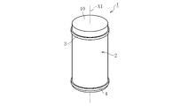
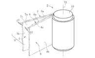
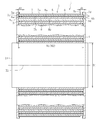
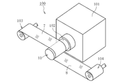
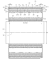
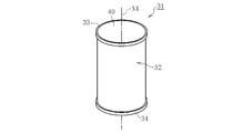
- FIG. 1 is a perspective view of a wound film capacitor according to a first embodiment of the present invention. It is a perspective view which shows the state which expanded a part of winding body shown in FIG. 1 virtually. It is sectional drawing of the winding type film capacitor shown in FIG. 1 is a perspective view showing an overall configuration of a wound body forming apparatus according to a first embodiment of the present invention. It is a figure for demonstrating an example of the winding aspect of a laminated
- FIG. 4 It is a figure for demonstrating an example of the winding aspect of a laminated
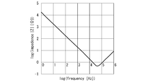
- FIG. 10 It is a perspective view which shows the state which expanded a part of winding body shown in FIG. 10 virtually. It is sectional drawing of the winding type film capacitor shown in FIG. It is a perspective view of the winding type film capacitor which concerns on 4th embodiment of this invention. It is sectional drawing of the winding type film capacitor shown in FIG. Sample No. 1 of Example 1 2 is a graph showing measurement results of impedance of a wound film capacitor according to 1;
- FIG. 1 is a perspective view of a wound film capacitor 1 according to a first embodiment of the present invention.
- the capacitor 1 includes a wound body 2 and positive and negative electrodes 3 and 4 that are in contact with the wound body 2 in the width direction (here, the direction is along the center line X1 of the wound body 2).
- Lead electrodes (not shown) are attached to the electrodes 3 and 4 so that a predetermined voltage can be applied between the electrodes 3 and 4.
- the configuration of the wound body 2 will be mainly described.
- the wound body 2 includes first and second conductive layers 5 and 6 and first and second insulating films 7 and 8.
- the conductive layers 5 and 6 and the first and second insulating films 7 and 8 are stacked in the order of the first conductive layer 5, the first insulating film 7, the second conductive layer 6, and the second insulating film 8. In the combined state, it is wound into a roll.
- the first and second conductive layers 5 and 6 are both metal films.
- the first and second insulating films 7 and 8 are both glass films.
- the first insulating film 7 has a first surface 7a oriented in one thickness direction and a second surface 7b oriented in the other thickness direction, and the first conductive layer 5 is on the first surface 7a. Is formed.
- the second insulating film 8 has a third surface 8a oriented in one thickness direction and a fourth surface 8b oriented in the other thickness direction, and a second conductive layer is formed on the third surface 8a. 6 is formed. Thereby, the first conductive layer 5 is integrated with the first insulating film 7, and the second conductive layer 6 is integrated with the second insulating film 8.
- the thickness t1 (see FIG. 2) of the glass film as the first insulating film 7 is set to 50 ⁇ m or less, preferably 40 ⁇ m or less, more preferably 30 ⁇ m or less, and further 20 ⁇ m or less. It is suitably set in the order of 10 ⁇ m or less, 8 ⁇ m or less, 6 ⁇ m or less, 5 ⁇ m or less, 3 ⁇ m or less, and particularly preferably 1 ⁇ m or less.
- the flexibility of the 1st insulating film 7 improves, so that the thickness dimension t1 is small, the minimum curvature radius of the said insulating film 7 can be made small to the level mentioned later.
- the thickness dimension t2 (refer FIG. 2) of the glass film as the 2nd insulating film 8 is set to 50 micrometers or less similarly to the glass film as the 1st insulating film 7, Preferably it sets to 40 micrometers or less. More preferably, it is set to 30 ⁇ m or less, more preferably 20 ⁇ m or less, 10 ⁇ m or less, 8 ⁇ m or less, 6 ⁇ m or less, 5 ⁇ m or less, 3 ⁇ m or less, and particularly preferably 1 ⁇ m or less.
- the first conductive layer 5 is directed to the first side end face 5a that faces one side in the width direction of the wound body 2 (left direction in FIG. 3) and the other side in the width direction (right direction in FIG. 3).
- the second conductive layer 6 has a third side end face 6 a that faces one side in the width direction of the wound body 2 and a fourth side end face 6 b that faces the other side in the width direction.
- the second side end face 5b of the first conductive layer 5 is offset to one side in the width direction from the fourth side end face 6b of the second conductive layer 6, and the second side end face 5b is offset.
- the third side end face 6 a of the conductive layer 6 is offset to the other side in the width direction from the first side end face 5 a of the first conductive layer 5.
- the offset amount of the first conductive layer 5, that is, the width direction dimension d1 of the region where the first conductive layer 5 is not formed on the first surface 7a of the first insulating film 7 is set to, for example, 1 mm or more. It is preferably set to 2 mm or more, more preferably 3 mm or more.
- the width direction dimension d2 of the region where the second conductive layer 6 is not formed in the third surface 8a of the second insulating film 8 which is the offset amount of the second conductive layer 6 is 1 mm or more.
- each conductive layer 5, 6 is not formed on the first surface 7 a of the first insulating film 7 and the third surface 8 a of the second insulating film 8.
- An insulating film having a thickness dimension equivalent to that of the layers 5 and 6 may be formed.
- the conductive layers 5 and 6 can be used for various materials.
- one or two or more metals selected from the group consisting of Al, Pt, Ni, Cu, Ag, and an Ag alloy can be suitably used, and among these, Ag is good
- an Ag alloy exhibits better heat resistance than Ag alone.
- the heat resistance is at least 50 ° C., preferably the heat resistance is 80 ° C., more preferably the heat resistance is 100 ° C.
- the first conductive layer 5 and the second conductive layer 6 are formed so as to have suitable heat resistance in the order of 200 ° C., 300 ° C., and 400 ° C., and particularly preferably 500 ° C. It is good.
- the heat resistance of each conductive layer 5 and 6 (metal film) can be evaluated by measuring the resistance value before and after the above-described heat treatment using a digital multimeter (M-04 manufactured by Custom Inc.). .
- the width direction dimension W2 of the 2nd insulating film 8 is equal to the width direction dimension W1 of the 1st insulating film 7, as shown in FIG.
- the first side end face 7c directed to one side in the width direction of the first insulating film 7, the third side end face 8c directed to one side in the width direction of the second insulating film 8, and the first The width direction positions of the second side end surface 7d directed to the other width direction of the one insulating film 7 and the fourth side end surface 8d directed to the other width direction of the second insulating film 8 can be aligned. Therefore, the electrodes 3 and 4 can be easily formed on both sides in the axial direction of the wound body 2.
- the first electrode 3 serving as a positive electrode or a negative electrode is disposed on one side in the width direction of the wound body 2.
- the first electrode 3 is electrically connected to the first conductive layer 5 adjacent in the thickness direction (vertical direction in FIG. 3) through the first insulating film 7 in the wound body 2.
- the second electrode 4 is disposed on the other side in the width direction of the wound body 2, is electrically connected to the second conductive layer 6, and is insulated from the first conductive layer 5. It is in contact with the fourth side end face 6b of the second conductive layer 6 (not in contact with the second side end face 5b of the first conductive layer 5).
- the electrodes 3 and 4 various materials can be used.
- one or two or more metals selected from the group consisting of Al, Pt, Ni, Cu, Ag, and an Ag alloy can be suitably used, and among these, Ag is good In particular, an Ag alloy exhibits better heat resistance than Ag alone.
- the first electrode 3 and the second electrode 4 should be formed so as to have suitable heat resistance in the order of 200 ° C., 300 ° C., and 400 ° C., and particularly preferably 500 ° C. .
- the electrodes 3 and 4 are formed, for example, by applying a conductive paste containing the above metal powder (a paste-like conductive material having a predetermined viscosity) on both sides in the axial direction of the wound body 2 and solidifying. It is possible.
- the conductive paste containing the metal powder may be made of only an inorganic material for the purpose of imparting heat resistance of at least 50 ° C. to the electrodes 3 and 4.
- the form that can be taken in this case is not particularly limited, and may be annular as shown in FIG. 1, or may be layered as shown in FIG. Of course, as shown in FIG. 1 and FIG. 3, it may be annular and layered.
- the minimum curvature radius of the first insulating film 7 in the wound body 2 is set to, for example, 100 mm or less, preferably 80 mm or less, more preferably 75 mm or less, and more specifically 50 mm or less, 30 mm or less, 20 mm or less, 10 mm or less. It is suitably set in the order of 5 mm or less, particularly preferably 3 mm or less.
- the outer diameter dimension of the wound body 2 is constant, the smaller the minimum winding diameter, the larger the area per unit volume, which is suitable for applications that require storage of a large amount of energy.
- the total length (longitudinal dimension) of the first insulating film 7 is set to, for example, 0.05 m or more, preferably set to 0.5 m or more, more preferably set to 1 m or more, and further to 3 m or more, It is suitably set in the order of 5 m or more, 10 m or more, 30 m or more, 50 m or more, 70 m or more, and particularly preferably 100 m or more.
- the width direction dimension W1 and the thickness dimension t1 are set such that the value obtained by dividing the width direction dimension W1 of the first insulating film 7 by the thickness dimension t1 is, for example, 1000 or more, and preferably 1200 or more.
- the width direction dimension W1 and the thickness dimension t1 are preferably set in order of preferably 1400 or more, more preferably 1600 or more, 1800 or more, and 2000 or more, and particularly preferably the width direction dimension W1 is 2400 or more.
- a thickness dimension t1 is set.
- the relative dielectric constant of the glass constituting the first insulating film 7 is set to, for example, 5 or more, preferably 5.5 or more, more preferably 6 or more, and further 7 or more. It is suitably set in the order of 8 or more, 9 or more, 10 or more, and particularly preferably 11 or more.
- the arithmetic average roughness Ra of the first surface 7a (second surface 7b) of the first insulating film 7 is set to, for example, 5 nm or less, preferably 3 nm or less, more preferably 1 nm or less, Furthermore, it is preferably set in the order of 0.8 nm or less, 0.4 nm or less, and 0.3 nm or less, and particularly preferably 0.2 nm or less.
- the maximum height Rmax of the first surface 7a (second surface 7b) of the first insulating film 7 is set to, for example, 10 nm or less, preferably 5 nm or less, and more preferably 3 nm or less.
- the maximum height Rmax of the first surface 7a (second surface 7b) of the first insulating film 7 refers to the value measured by the method based on JIS B0601: 2001.
- the first insulating film 7 has a glass composition in mass%, for example, SiO 2 : 20 to 70%, Al 2 O 3 : 0 to 20%, B 2 O 3 : 0 to 17%, MgO: 0 to 10%, CaO: 0 to 15%, SrO: 0 to 15%, BaO: 0 to 40%.
- the content of SiO 2 exceeds the appropriate range and increases, the meltability and moldability may be reduced.
- the content of SiO 2 is set to 70% or less, preferably 65% or less, more preferably 60% or less, and further 58% or less, 55% or less, 50%. It is suitably set in the following order, particularly preferably 45% or less.
- the content of SiO 2 falls outside the proper range, it becomes difficult to form a glass network structure, and vitrification may become difficult.
- the content of SiO 2 is set to 20% or more, preferably 25% or more, particularly preferably 30% or more.
- the content of Al 2 O 3 is set to 20% or less, preferably set to 18% or less, more preferably set to 15% or less, and further preferably set to 12% or less. Preferably, it is set to 10% or less.
- the content of Al 2 O 3 falls outside the appropriate range and decreases, the component balance of the glass composition is impaired and the glass tends to be devitrified, depending on the relationship with other components.
- the content of Al 2 O 3 is set to 0% or more, preferably 1% or more, more preferably 3% or more, and particularly preferably 5% or more.
- the content of B 2 O 3 When the content of B 2 O 3 increases outside the proper range, the dielectric constant tends to decrease, the heat resistance decreases, and the reliability of the wound film capacitor 1 in a high temperature environment may decrease. Arise.
- the content of B 2 O 3 is set to 17% or less, preferably set to 15% or less, more preferably set to 13% or less, more specifically 11% or less, 7% or less. It is preferably set in order, and particularly preferably 5% or less.
- MgO is a component that increases the strain point and decreases the high-temperature viscosity.
- the content of MgO increases outside the appropriate range, the liquidus temperature, density, and thermal expansion coefficient tend to be excessively high.
- the content of MgO is set to 10% or less, preferably 5% or less, more preferably 3% or less, more specifically 2% or less, 1.5% or less, 1 % Is preferably set in the order of% or less, and particularly preferably 0.5% or less.
- the CaO content is set to 15% or less, preferably 12% or less, more preferably 10% or less, still more preferably 9% or less, and particularly preferably 8%. Set to less than 5%.
- the content of CaO is set to 0% or more, preferably 0.5% or more, more preferably 1% or more, and further 2% to 3% in this order. And is preferably set to 5% or more.
- the SrO content is set to 15% or less, preferably 12% or less.
- the SrO content is set to 0% or more, preferably set to 0.5% or more, more preferably set to 1% or more, still more preferably set to 3% or more, particularly preferably. Is set to 5% or more.
- the BaO content is set to 40% or less, preferably 35% or less.
- the content of BaO is set to 0% or more, preferably 0.5% or more, more preferably 1% or more, and further 2% or more, 5% or more, 10% % Or more, 15% or more, and 20% or more in order, particularly preferably 25% or more.
- Each component of MgO, CaO, SrO, and BaO is a component that increases the dielectric constant, devitrification resistance, meltability, and moldability.
- the content of MgO + CaO + SrO + BaO (total amount of MgO, CaO, SrO, BaO) decreases outside the appropriate range, it becomes difficult to increase the dielectric constant, and the function as a flux cannot be sufficiently exhibited. , The meltability tends to decrease.
- the content of MgO + CaO + SrO + BaO is set to 5% or more, preferably 10% or more, more preferably 15% or more, and more preferably 20% or more and 25% or more in this order. And particularly preferably 30% or more.
- the content of MgO + CaO + SrO + BaO increases outside the appropriate range, the density tends to increase, and the balance of the glass composition component is impaired, and conversely, devitrification resistance tends to decrease.
- the content of MgO + CaO + SrO + BaO is set to 60% or less, preferably 55% or less, and more preferably 50% or less.
- the following components can be added to the glass composition within a range of appropriate content ratios.
- Each component of Li 2 O, Na 2 O, and K 2 O is a component that reduces the viscosity and adjusts the thermal expansion coefficient. However, if it is included in a large amount outside the appropriate range, a voltage that causes dielectric breakdown. Tends to decrease. In addition, the temperature characteristics of dielectric constant tend to decrease. For these reasons, when these components are added, the total amount is set to 15% or less, preferably 10% or less, more preferably 5% or less, and further to 2% or less, It is preferably set in the order of 1% or less and 0.5% or less, particularly preferably 1000 ppm or less.
- the ZnO is a component that increases the dielectric constant and also increases the meltability. However, if it is included in a large amount outside the appropriate range, devitrification of the glass tends to occur and the density tends to increase. For these reasons, the ZnO content is set to 0 to 40%, preferably 0 to 30%, more preferably 0 to 20%, and even more preferably 0.5 to 15%. Particularly preferably, it is set to 1 to 10%.
- ZrO 2 is a component that increases the dielectric constant. However, if the ZrO 2 is included outside the proper range and contained in a large amount, the liquidus temperature rises abruptly and zircon devitrified foreign matter tends to precipitate. For the above reasons, the content of ZrO 2 is set to 20% or less, preferably 15% or less, and more preferably 10% or less. Further, the content of ZrO 2 is set to 0.1% or more, preferably set to 0.5% or more, more preferably set to 1% or more, still more preferably set to 2% or more, and particularly preferably Is set to 3% or more.
- Each component of Y 2 O 3 , Nb 2 O 3 , and La 2 O 3 is a component that increases the dielectric constant and the like. However, if it is included in a large amount outside the appropriate range, the density tends to increase. For the above reasons, when adding Y 2 O 3 , Nb 2 O 3 , La 2 O 3 , the content of each component is preferably set to 20% or less.
- the glass composition of the first insulating film 7 includes one or two selected from the group consisting of As 2 O 3 , Sb 2 O 3, CeO 2 , SnO 2 , F, Cl, and SO 3 as a fining agent.
- the above can be added in the range of 0 to 3%. However, it is preferable to refrain from using As 2 O 3 , Sb 2 O 3 , and F as much as possible from the environmental viewpoint, and the content of each component is preferably set to less than 0.1%. From the environmental point of view, SnO 2 , Cl and SO 3 are preferable as the fining agent.
- the content of SnO 2 + Cl + SO 3 (the total amount of SnO 2 , Cl and SO 3 ) is set to 0.001 to 1%, preferably set to 0.01 to 0.5%, more preferably 0.00. It is set to 01 to 0.3%. Further, the SnO 2 content is set to 0 to 1%, preferably set to 0.01 to 0.5%, particularly preferably set to 0.05 to 0.4%.
- components other than those described above can be added to the glass composition of the first insulating film 7 in a range of, for example, up to 20%, preferably up to 10%.
- the liquidus temperature of the glass which comprises the 1st insulating film 7 is set to 1200 degrees C or less, for example, Preferably it is set to 1150 degrees C or less, More preferably, it is set to 1090 degrees C or less, Furthermore, it is 1050 degrees C or less, 1030 It is suitably set in the order of °C or less, particularly preferably 1000 °C or less. If the liquid phase temperature of the first insulating film 7 is too high, the glass tends to be devitrified during molding, and it becomes difficult to improve the surface accuracy (surface roughness, etc.) of the first insulating film 7. is there.
- the liquid phase viscosity of the first insulating film 7 is set to, for example, 10 3.5 dPa ⁇ s or more, preferably 10 4.0 dPa ⁇ s or more, and more preferably 10 4.5 dPa ⁇ s. It is set as described above, more preferably 10 4.8 dPa ⁇ s or more, and particularly preferably 10 5.0 dPa ⁇ s or more. This is because if the liquid phase viscosity of the first insulating film 7 is too low, devitrification of the glass tends to occur during molding, and it becomes difficult to increase the surface accuracy of the first insulating film 7.
- the liquid phase viscosity refers to a value obtained by measuring the viscosity of glass at the liquid phase temperature by a platinum ball pulling method.
- the liquid phase temperature passes through a standard sieve 30 mesh (about 500 ⁇ m), the glass powder remaining in 50 mesh (about 300 ⁇ m) is placed in a platinum boat and held in a temperature gradient furnace for 24 hours, and crystals precipitate. Refers to the value measured temperature.
- the density of the glass which comprises the 1st insulating film 7 is set to 4.5 g / cm ⁇ 3 > or less, for example, Preferably it is set to 4.0 g / cm ⁇ 3 > or less, More preferably, it sets to 3.6 g / cm ⁇ 3 > or less. Further, 3.3 g / cm 3 or less, 3.0 g / cm 3 or less, preferably 2.8 g / cm 3 or less, and particularly preferably 2.5 g / cm 3 or less. . The smaller the density, the easier it is to reduce the weight of the wound film capacitor 1. In addition, the density here refers to the value measured by the well-known Archimedes method.
- the coefficient of thermal expansion of the glass constituting the first insulating film 7 is set to, for example, 25 ⁇ 10 ⁇ 7 to 120 ⁇ 10 ⁇ 7 / ° C., preferably 30 ⁇ 10 ⁇ 7 to 120 ⁇ 10 ⁇ 7 / ° C. More preferably, it is set to 40 ⁇ 10 ⁇ 7 to 110 ⁇ 10 ⁇ 7 / ° C., more preferably 60 ⁇ 10 ⁇ 7 to 100 ⁇ 10 ⁇ 7 / ° C., and particularly preferably 70 ⁇ 10 ⁇ 7. It is set to ⁇ 95 ⁇ 10 ⁇ 7 / ° C.
- the coefficient of thermal expansion of the first insulating film 7 is set in the above range, the coefficient of thermal expansion of the first insulating film 7 and the surfaces 7a and 7b of the first insulating film 7 are formed by film formation or the like. Since the thermal expansion coefficients of the conductive layers 5 and 6 can be matched (approached), deformation of the conductive layers 5 and 6 such as warpage can be prevented.
- the coefficient of thermal expansion here refers to an average value measured with a dilatometer in the range of 30 to 380 ° C.
- the temperature at 10 2.5 dPa ⁇ s of the glass constituting the first insulating film 7 is set to, for example, 1550 ° C. or lower, preferably 1450 ° C. or lower, more preferably 1350 ° C. or lower, More specifically, it is suitably set in the order of 1250 ° C. or lower, 1200 ° C. or lower, 1170 ° C. or lower, and particularly preferably 1150 ° C. or lower.
- the lower the temperature of the first insulating film 7 at 10 2.5 dPa ⁇ s the easier it is to melt the glass at a lower temperature, so the manufacturing cost of the glass film can be reduced.
- the temperature at 10 2.5 dPa ⁇ s refers to a value measured by a platinum ball pulling method.
- At least part of the first surface 7a (second surface 7b) of the first insulating film 7 may be in an unpolished state. Moreover, in that case, it is preferable that all of the first surface 7a and the second surface 7b directed in opposite directions are unpolished.
- the theoretical strength of glass is very high, in fact, it often breaks at much lower stresses than the theoretical strength. This is because a small defect called Griffith flow is generated on the surface of the glass in a post-molding process such as a polishing process. Therefore, if the first surface 7a (second surface 7b) of the first insulating film 7 which is a glass film is unpolished, in other words, the surface 7a (7b) is called a molding surface (fire-making surface).
- the mechanical strength of the glass can be brought close to the original strength, thereby preventing the glass film from being broken as much as possible.
- the insulating film 7 having the first surface 7a (second surface 7b) that is unpolished and excellent in surface accuracy is formed by molding a glass film by a redraw method or an overflow downdraw method described later. Can be obtained.
- the thickness dimension t1 of the first insulating film 7 can be easily reduced. Further, the surface quality of the first insulating film 7 can be improved. Furthermore, the 1st and 2nd side end surface 7c, the 1st insulating film 7 makes the 1st and 2nd side end surface 7c, 7d (refer FIG. 3) of the 1st insulating film 7 into a shaping
- the redraw method is a method in which a molded glass is heated again to a temperature near the softening point and stretched to form the glass into a predetermined shape (in the case of this embodiment, a long film). Say.
- glass film forming means other than redraw such as an overflow down draw method or a slot down draw method
- the overflow down-draw method is a forming method called fusion method, in which molten glass overflows from both sides of the heat-resistant bowl-like structure, and the overflowing molten glass is joined at the lower end of the bowl-like structure.
- this is a method of obtaining glass having a predetermined shape (long glass film in the case of the present embodiment) by stretching downward. Surface quality can also be improved by forming a glass film by the overflow downdraw method.
- the second insulating film 8 is a glass film
- at least one of the glass composition, physical properties, molding conditions, and the like of the first insulating film 7 described above can be made the same.
- glass films having different glass compositions, physical properties, molding conditions, and the like may be used for the second insulating film 8 as long as there is no particular problem in terms of cost and productivity.
- the material (glass composition) of both the insulating films 7 and 8 was described, as long as it can wind up without generating a crack, not only the glass composition mentioned above but various materials are also employable. It is. Specific examples include alkali-free glass, soda glass, and alkali-containing glass.
- the thickness dimension t2 of the 2nd insulating film 8 is arbitrary, when the 2nd insulating film 8 is used as a glass film, relative of the 2nd insulating film 8 with respect to the thickness dimension t1 of the 1st insulating film 7
- the thickness dimension t2 is set so that the thickness dimension (a value obtained by dividing the thickness dimension t2 of the second insulating film 8 by the thickness dimension t1 of the first insulating film 7) is, for example, 0.3 or more, and preferably is set to a value of about 0.1.
- the thickness dimension t2 is suitably set in the order of 0.6 or more, 0.7 or more, and 0.8 or more so as to be 4 or more, more preferably 0.5 or more, and particularly preferably 0.
- the thickness dimension t2 is set to be 9 or more.
- the thickness dimension t2 of the second insulating film 8 is set so that the ratio of the thickness dimensions t1 and t2 is, for example, 3.0 or less, preferably 2.5 or less. More preferably, the thickness dimension t2 is suitably set in the order of 1.8 or less, 1.5 or less, 1.3 or less, 1.2 or less, 1.1 or less, more preferably 2.0 or less. Particularly preferably, the thickness dimension t2 is set to be 1.05 or less.
- the center of the wound body 2 it extends in the direction along the width direction of the wound body 2, in the direction along the center line X ⁇ b> 1 of the wound body 2 in FIG. 2, and the inner peripheral surface of the wound body 2 A contacting core 10 is provided.
- the center line of the core 10 is equal to the center line X1 of the wound body 2 (see FIGS. 1 and 2).
- the outer diameter D1 of the core 10 is substantially equal to the minimum radius of curvature of any of the above-described insulating films. In this embodiment, as shown in FIG.
- the core 10 has a form that protrudes (projects) from both end surfaces in the width direction of the wound body 2. As long as it can be formed accurately, it is possible to take a form that protrudes only to one side in the width direction of the wound body 2 or does not protrude from the end face in the width direction of the wound body 2 (winding). It is also possible that the width direction end face of the body 2 and the end face of the core 10 are on the same plane level.
- FIG. 4 is a perspective view showing the entire configuration of the wound body forming apparatus 100 used for forming the wound body 2.
- This wound body forming apparatus 100 is connected to a drive device 101 such as a motor and a rotation drive shaft 102 of the drive device 101 and rotates integrally with the rotation drive shaft 102, that is, a wound body forming core, that is, FIG.
- a roll body 103 of the first insulating film 7 and a roll body 104 of the second insulating film 8 are disposed around the rotary drive shaft 102 and the core 10.
- the first insulating film 7 and the second insulating film 8 can be pulled out to different positions (circumferential positions) on the outer peripheral surface of the core 10, specifically, the outer periphery of the core 10.
- Both roll bodies 103 and 104 are disposed at positions where the drawing positions on the surface can be drawn at positions that are 180 degrees different in the circumferential direction (the phase is shifted by 180 degrees).
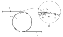
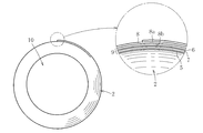
- the winding of the laminated film 9 using the wound body forming apparatus 100 having the above configuration is performed as follows, for example. First, as shown in FIG. 5, one end 8e in the longitudinal direction of the second insulating film 8 serving as the winding start side end is brought into close contact with the outer peripheral surface of the core 10 serving as the winding surface, and the rotation drive shaft 102 is disposed. By rotating around the axis, the core 10 (see FIG. 4) connected to the rotation drive shaft 102 is rotated, and winding of the second insulating film 8 is started. Then, when the second insulating film 8 is wound, for example, about 0.5 turn (1/2 turn) to about 3 turns (about 2 turns in FIG. 5), the first insulating film 7 is turned into the second insulation film.
- Winding of the laminated film 9 formed on the film 8 is started.
- the winding of the second insulating film 8 is started.
- the outer surface (third surface 8a) and the inner surface (fourth surface 8b) of the second insulating film 8 are in close contact with each other.
- the formation region of the second conductive layer 6 is preferably set.
- the inner surface (second surface 7b) of the first insulating film 7 and the second insulating film 8 at the one end portion 7e in the longitudinal direction that is the winding start side end portion of the first insulating film 7 is preferably set so that the outer surface (third surface 8a) is in direct contact with the outer surface.
- the amount of preceding winding of the 2nd insulating film 8 is not restricted to the said illustration, For example, 0.1 rounds, 0.25 rounds, 1 round, 1.5 rounds, 5 rounds, etc. arbitrary The amount of winding can be set.
- the fixing means for the first and second insulating films 7 and 8 is arbitrary.
- the second insulating film 8 is continuously moved to 0, for example. .5 rounds (1/2 round) to about 3 rounds (about 2 rounds in FIG. 6) are wound, so that the outer surface (third surface 8a) and the inner surface (second surface) of the second insulating film 8 are wound.
- the four surfaces 8b) are fixed to each other by direct contact.
- the wound body 2 in the state in which the winding form of both the insulating films 7 and 8 is maintained can be obtained.
- the additional winding amount on the winding end side of the second insulating film 8 is not limited to the above-described example, and for example, 0.1 turn, 0.25 turn, 1 turn, 1.5 turn, An arbitrary winding amount such as 5 laps can be used.
- both positive and negative electrodes 3 and 4 are formed on both sides of the wound body 2 in the axial direction.
- the first electrode 3 is in contact with the first side end face 5a of the first conductive layer 5 and the third side end face 6a of the second conductive layer 6 as shown in FIG. Not formed.
- the second electrode 4 is formed so as to be in contact with the fourth side end face 6 b of the second conductive layer 6 and not in contact with the second side end face 5 b of the first conductive layer 5.
- both the positive and negative electrodes 3 and 4 are formed so as to cover both ends in the width direction of the wound body 2, and only the corresponding conductive layers 5 and 6 are electrically connected.
- the wound film capacitor 1 is completed.
- the formation means of the electrodes 3 and 4 is arbitrary, from a viewpoint which implement
- the first and second insulating films 7 and 8 and the first and second conductive layers 5 and 6 are wound in a roll shape in a state where the first and second conductive layers 5 and 6 are alternately overlapped.
- the revolving body 2 constitutes the capacitor 1 and at least the first insulating film 7 is a glass film. Since glass is unlikely to generate oxygen vacancies, the temperature dependence of the dielectric constant can be reduced without reducing the dielectric constant. Therefore, the electrostatic capacity per unit volume of the capacitor 1 is increased by configuring the capacitor 1 with the wound body 2 in a form in which the insulating film 7 made of glass is rolled up with the conductive layers 5 and 6. However, a situation in which the circuit does not operate properly due to a temperature change can be effectively prevented. Therefore, the capacitor 1 that can store a large amount of energy and has excellent high-temperature environment characteristics can be manufactured in a relatively small size.
- the first insulating film 7 and the second insulating film 8 are glass films, and the first and second conductive layers 5 and 6 are both metal films. And while forming the 1st conductive layer 5 in the 1st surface 7a which faces the thickness direction one side of the 1st insulating film 7, the 3rd surface 8a which faces the thickness direction one side of the 2nd insulating film 8 The 2nd conductive layer 6 was formed in this, and what wound these 2 sheets of insulation films 7 and 8 on each other was wound up in roll shape, and the wound body 2 was formed.
- the first insulating film 7 and the second insulating film 8 are overlapped and wound so that the first conductive layer 5 and the second conductive layer 6 do not come into contact with each other.
- the function of can be demonstrated appropriately.
- one metal film is integrally formed for one glass film (the first conductive layer 5 is integrally formed on the first insulating film 7 and the second conductive layer 6 is integrally formed on the second insulating film 8.
- the bending stress of the glass film is reduced compared to the case where a metal film is formed on both surfaces of one glass film, so the probability of breakage is reduced. It can be kept low and stable production becomes possible.
- the 1st and 2nd insulating film 7 and 8 can be wound around the core 10 to easily maintain the state in which the wound body 2 is formed. Therefore, it is possible to obtain a high-performance wound film capacitor 1 while maintaining the shape accuracy when winding the wound body 2.
- wound film capacitor according to the present invention is not limited to the above embodiment, and can take various forms within the scope of the present invention. It is.
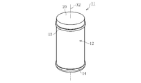
- FIG. 7 is a perspective view of a wound film capacitor 11 according to the second embodiment of the present invention.
- This capacitor 11 has a wound body 12, and positive and negative electrodes 13, 14 that are in contact with the wound body 12 in the width direction (here, coincides with the direction along the center line X 2 of the wound body 12).
- a lead wire (not shown) is attached to each of the electrodes 13 and 14 so that a predetermined voltage can be applied between the electrodes 13 and 14.
- the difference from the first embodiment will be mainly described.
- the wound body 12 includes first and second conductive layers 15 and 16 and first and second insulating films 17 and 18, and these two conductive layers 15 and 16. And the two insulating films 17 and 18 are laminated in the order of the first conductive layer 15, the first insulating film 17, the second conductive layer 16, and the second insulating film 18 (as a laminated film 19). Formed in the form of a roll.
- the first and second conductive layers 15 and 16 are both metal films, and the first surface 17 a and the second surface are oriented in opposite directions in the thickness direction of the first insulating film 17. 17b is formed. Thereby, both the first and second conductive layers 15 and 16 are integrated with the first insulating film 17.
- the first insulating film 17 is a glass film.
- the two conductive layers 15 and 16 are integrated with this glass film.
- the thickness t3 (see FIG. 8) of the glass film as the first insulating film 17 is set to 50 ⁇ m or less, preferably 40 ⁇ m or less, more preferably 30 ⁇ m or less, and further 20 ⁇ m or less. It is suitably set in the order of 10 ⁇ m or less, 8 ⁇ m or less, 6 ⁇ m or less, 5 ⁇ m or less, 3 ⁇ m or less, and particularly preferably 1 ⁇ m or less.
- the second insulating film 18 is a resin film.
- Various materials can be used as the resin film.
- one or more selected from the group of PET (polyethylene terephthalate), PEN (polyethylene naphthalate), PP (polypropylene), polycarbonate, polyimide, polyphenylene sulfide are preferable.
- PET polyethylene terephthalate
- PEN polyethylene naphthalate
- PP polypropylene
- PET is preferred.
- the thickness dimension t4 of the second insulating film 18 is arbitrary, but for example, it is set to an appropriate size so as to be extremely thin or not thicker than the thickness dimension t3 of the first insulating film 17. .
- the width direction dimension W4 of the 2nd insulating film 18 (resin film) in which the conductive layers 15 and 16 are not formed is the width direction of the 1st insulating film 17, as shown in FIG.
- the first insulating film 17 is smaller than the dimension W3 and is disposed so as to protrude from the second insulating film 18 to the outside in the width direction. In this way, it is possible to avoid the state in which the second insulating film 18 protrudes in the axial direction of the wound body 12 rather than the conductive layers 15 and 16, so that the electrodes 13 and 14 are disposed on both sides in the axial direction of the wound body 12. Can be easily formed.
- the arrangement form including the offset aspects of the first and second conductive layers 15 and 16 (the positional relationship in the width direction of the side end faces 15a, 15b, 16a and 16b, the magnitude of the offset amounts d3 and d4) is as follows. Since it is the same as 1st embodiment, description is abbreviate
- the materials of the conductive layers 15 and 16 are the same as those in the first embodiment, the description thereof is omitted here.
- first and second electrodes 13 and 14 including the form of contact with the respective conductive layers 15 and 16
- material are the same as those in the first embodiment, so the description thereof is omitted here.
- the minimum curvature radius, the total length, the ratio of the thickness dimension t3 to the width direction dimension W3, the relative dielectric constant, the arithmetic average roughness Ra of the first surface 17a (second surface 17b), the maximum The height Rmax, the glass composition, the liquidus temperature, the thermal expansion coefficient, the viscosity, the surface properties, and the molding means are also the same as those in the first embodiment, and thus description thereof is omitted here.
- the winding body 12 extends in the direction along the width direction of the wound body 12, that is, the direction along the center line X ⁇ b> 2 of the wound body 12 in FIG. 9.
- a core 20 in contact with the inner peripheral surface of the body 12 is provided.
- the center line of the core 20 is equal to the center line X2 of the wound body 12 (see FIGS. 8 and 9).
- the outer peripheral surface of the core 20 is in contact with the innermost insulating film of the first insulating film 17 and the second insulating film 18 (see FIG. 9).
- the outer diameter D2 of the core 20 is substantially equal to the minimum radius of curvature of any of the insulating films described above.
- the presence or absence of protrusion from the wound body 12 of the core 20 is arbitrary.
- the wound film capacitor 11 having the above-described configuration can be manufactured by, for example, the same method as in the first embodiment.
- the first insulating film 17 is a glass film
- the second insulating film 18 is a resin film.
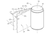
- FIG. 10 is a perspective view of a wound film capacitor 21 according to the third embodiment of the present invention.
- the capacitor 21 has a wound body 22 and positive and negative electrodes (described later) that are in contact with the wound body 22 in the width direction (here, coincides with the direction along the center line X3 of the wound body 22).
- Each electrode is provided with a lead wire (not shown) so that a predetermined voltage can be applied between the electrodes.
- the difference from the first and second embodiments will be mainly described.
- the wound body 22 includes metal films 25 and 26 as first and second conductive layers and first and second insulating films 27 and 28.
- the metal films 25 and 26 and the two insulating films 27 and 28 are superposed in the order of the first metal film 25, the first insulating film 27, the second metal film 26, and the second insulating film 28 ( As a laminated film 29), the film is wound into a roll.
- the first and second metal films 25 and 26 are sandwiched between the insulating films 27 and 28 independently of the first and second insulating films 27 and 28. .
- the first metal film 25 protrudes to one side in the width direction of the wound body 22 from the first and third side end faces 27c, 28c of the insulating films 27, 28.
- the first protruding portion 23 is bent and is in contact with the first metal film 25 adjacent in the radial direction of the wound body 22.
- the second metal film 26 protrudes to the other side in the width direction of the wound body 22 from the second and fourth side end faces 27d, 28d of the respective insulating films 27, 28, and this second The protruding portion 24 is bent and is in contact with the second metal film 26 adjacent in the radial direction of the wound body 22.
- the first protruding portion 23 is a first electrode that contacts the wound body 2 on one side in the width direction
- the second protruding portion 24 is a second electrode that contacts the wound body 22 on the other side in the width direction.
- the arrangement form including the offset forms of the first and second conductive layers (metal films) 25, 26 (the positional relationship in the width direction of each side end face 25a, 25b, 26a, 26b, the magnitude of the offset amounts d5, d6) ) Is the same as in the first and second embodiments, the description thereof is omitted here.
- metal films 25 and 26 having the above-described configuration.
- metal films 25 and 26 having the above-described configuration.
- an aluminum film is preferable.
- the two insulating films 27 and 28 are both glass films.
- the width-direction dimensions W5 and W6 (see FIG. 12) of the two insulating films 27 and 28 (glass film) are the same.
- the thickness dimensions t5 and t6 (see FIG. 11) of the first and second insulating films 27 and 28 are the same as those in the first embodiment, description thereof is omitted here.
- the height Rmax, the glass composition, the liquidus temperature, the thermal expansion coefficient, the viscosity, the surface properties, and the molding means are also the same as those in the first and second embodiments, and thus the description thereof is omitted here.
- the center of the wound body 22 extends in the direction along the width direction of the wound body 22, that is, in the direction along the center line X3 of the wound body 22 in FIG.
- a core 30 that contacts the inner peripheral surface of the wound body 22 is provided.
- the center line of the core 30 is equal to the center line X3 of the wound body 22 (see FIGS. 11 and 12).
- the outer peripheral surface of the core 30 is in contact with the insulating film located on the innermost side of the first insulating film 27 and the second insulating film 28 (see FIG. 12).
- the outer diameter D3 of the core 30 is substantially equal to the minimum radius of curvature of any of the insulating films described above.
- the presence or absence of protrusion from the wound body 22 of the core 30 is arbitrary.
- the wound film capacitor 21 having the above-described configuration can be manufactured by, for example, the same method as in the first embodiment.
- the two metal films 25 and 26 and the two insulating films (glass films) 27 and 28 are divided into the first metal film 25, the first insulating film 27, the second metal film 26, and the second one.
- the wound body 22 was formed by winding in the state of overlapping the two insulating films 28 in order. According to this configuration, contact between the metal films 25 and 26 can be effectively avoided.
- the bending stress of the glass film which arises at the time of winding can be relieve
- the wound body 22 includes a laminated unit in the order of the first metal film 25, the first insulating film 27, the second metal film 26, and the second insulating film 28.
- a glass film and a metal film may be further laminated.
- the first metal film 25 may be wound as the outermost layer, or the first metal film 25 may be wound as the innermost layer.
- FIG. 13 is a perspective view of a wound film capacitor 31 according to the fourth embodiment of the present invention.
- the capacitor 31 has a wound body 32, and positive and negative electrodes 33 and 34 that are in contact with the wound body 32 in the width direction (here, coincide with the direction along the center line X4 of the wound body 32).
- a lead wire (not shown) is attached to each electrode 33, 34 so that a predetermined voltage can be applied between the electrodes 33, 34.
- the description will focus on differences from the first to third embodiments.
- the wound body 32 includes first and second conductive layers 35 and 36 and first and second insulating films 37 and 38, and these two conductive layers 35 and 36. And the two insulating films 37 and 38 are laminated in the order of the first conductive layer 35, the first insulating film 37, the second conductive layer 36, and the second insulating film 38 (as a laminated film 39). Formed in the form of a roll.
- the first and second conductive layers 35 and 36 are both metal films, and the first surface 37a and the second surface are oriented in opposite directions in the thickness direction of the first insulating film 37. 37b, respectively. Thereby, both the first and second conductive layers 35 and 36 are integrated with the first insulating film 37.
- the first insulating film 37 is a glass film.
- the two conductive layers 35 and 36 are integrated with this glass film.
- the thickness t3 (see FIG. 8) of the glass film as the first insulating film 37 is set to 50 ⁇ m or less, preferably set to 40 ⁇ m or less, more preferably set to 30 ⁇ m or less, and more specifically 20 ⁇ m or less. It is suitably set in the order of 10 ⁇ m or less, 8 ⁇ m or less, 6 ⁇ m or less, 5 ⁇ m or less, 3 ⁇ m or less, and particularly preferably 1 ⁇ m or less.
- the second insulating film 38 for example, a resin, paper, or glass film can be used, and among these, a glass film (that is, a glass film) can be suitably used.
- a glass film for the second insulating film 38 as well, it is possible to eliminate the so-called organic matter and form the wound body 32 with only the inorganic material, so that the heat resistance of the wound film capacitor 31 is improved. It can be easily increased.
- the thickness dimension t4 (see FIG. 8) of the glass film (second insulating film 38) is the same as the glass film as the first insulating film 37.
- it is set to 50 ⁇ m or less, preferably set to 40 ⁇ m or less, more preferably set to 30 ⁇ m or less, more preferably 20 ⁇ m or less, 10 ⁇ m or less, 8 ⁇ m or less, 6 ⁇ m or less, 5 ⁇ m or less, 3 ⁇ m or less. And particularly preferably 1 ⁇ m or less.
- the width direction dimension W8 of the 2nd insulating film 38 (resin film) in which the conductive layers 35 and 36 are not formed is the width direction of the 1st insulating film 37, as shown in FIG.
- the first insulating film 37 is smaller than the dimension W7 and is disposed so as to protrude from the second insulating film 38 to the outside in the width direction.
- the arrangement form including the offset aspects of the first and second conductive layers 35 and 36 (the positional relationship in the width direction of each side end face 35a, 35b, 36a, 36b, the magnitude of the offset amounts d7, d8) is as follows. Since this is the same as in the first to third embodiments, description thereof is omitted here.
- the materials of the conductive layers 35 and 36 are the same as those in the first to third embodiments, the description thereof is omitted here.
- the first and second electrodes 33 and 34 (including the form of contact with the respective conductive layers 35 and 36) and materials are also the same as those in the first to third embodiments. Omitted.
- the minimum curvature radius, the total length, the ratio of the thickness dimension t3 to the width direction dimension W7, the relative dielectric constant, the arithmetic average roughness Ra of the first surface 37a (second surface 37b), the maximum The height Rmax, the glass composition, the liquidus temperature, the thermal expansion coefficient, the viscosity, the surface properties, and the molding means are also the same as those in the first to third embodiments, and thus the description thereof is omitted here.
- the second insulating film 38 is a glass film
- at least one of the glass composition, physical properties, shape, surface properties, dimensions, molding conditions, etc. of the first insulating film 37 described above can be made the same. It is.
- glass films having different glass compositions, physical properties, shapes, surface properties, dimensions, molding conditions, etc. may be used for the second insulating film 38. .
- the through hole 40 penetrates the wound body 32 in the direction along the width direction of the wound body 32, that is, in the direction along the center line X4 of the wound body 32 in FIG. Is provided.
- the through hole 40 penetrates not only the wound body 32 but also the electrodes 33 and 34 attached to both sides in the width direction. Therefore, as shown in FIG. 13, the through hole 40 penetrates the wound film capacitor 31 in the direction along the center line at the center of the wound film capacitor 31.
- the center line of the wound film capacitor 31 is equal to the center line X4 of the wound body 32 (see FIGS. 13 and 14).
- the internal diameter dimension D4 of the through hole 40 in this case Is approximately equal to the minimum radius of curvature of the insulating film 38 described above.
- the wound film capacitor 31 having the above-described configuration forms, for example, a wound body 32 integrally with a core (not shown) as shown in FIG. 1 in the same manner as in the first embodiment. And the electrodes 33 and 34 are provided on both sides in the width direction.
- a through hole 40 penetrating the wound body 32 in the width direction is provided at the center of the wound body 32 constituting the wound film capacitor 31.
- a hollow space that is, air as an insulator exists in the center of the wound film capacitor 31 over the entire width direction.
- the winding body 32 may be affected by the core when operated like a kind of coil. Inductance may increase. This kind of increase in inductance is not preferable because it causes an increase in impedance particularly in a high frequency range.
- the through hole 40 at the center of the wound body 32 as described above, air as an insulator exists inside the wound body 32, so that the increase in inductance as described above is achieved. It is possible to suppress the increase in impedance in the high frequency region as much as possible.
- the center of the wound body 32 is a hollow space, the wound film capacitor 31 can be reduced in weight by that amount, which is also suitable for general use of the capacitor 31.
- the first insulating films 7, 17, 27, 37 and the second insulating film are used as the wound bodies 2, 12, 22, 32 of the wound film capacitors 1, 11, 21, 31.
- 8, 18, 28, and 38 are wound into a true cylinder
- other shapes may be used as a matter of course.
- the first insulating films 7, 17, such as an elliptical winding body and a flat winding body including a straight portion when viewed from the direction along the center line, As long as 27, 37 and the second insulating films 8, 18, 28, 38 are wound up in a roll shape, various forms can be taken.
- Example 1 of the present invention will be described.
- the density was measured by the well-known Archimedes method.
- strain point and annealing point were measured by a method based on ASTM C336-71.
- the softening point was measured by a method based on ASTM C338-93.
- the high temperature viscosity 10 4.0 dPa ⁇ s, 10 3.0 dPa ⁇ s, and the temperature at 10 2.5 dPa ⁇ s, was measured by a platinum ball pulling method.
- the thermal expansion coefficient was measured with a dilatometer in the range of 30 to 380 ° C.
- the glass powder that passes through a standard sieve 30 mesh (about 500 ⁇ m) and remains in 50 mesh (about 300 ⁇ m) is placed in a platinum board and held in a temperature gradient furnace for 24 hours, and the temperature at which crystals precipitate. was measured.
- the viscosity of the glass at the liquid phase temperature was measured by a platinum ball pulling method.
- the dielectric constant was measured by a method based on ASTM D150.
- the thickness dimension is 45 nm.
- a Cu film was formed by film formation. At the time of film formation, a region (width direction dimension d1 in FIG. 3) from one side surface up to 3 mm from the second side end face was masked so that a Cu film was not formed on the masking portion. Further, a region (width direction dimension d2 in FIG. 3) from the first side end surface of the other surface to 3 mm was masked to prevent the Cu film from being formed on the masking portion. In this way, after the Cu film was formed, the masking portion was removed.
- the substrate glass film and the interposed glass film were overlapped, and the overlapped body was wound around the outer peripheral surface of an insulating tube as a core having an outer diameter of 50 mm, thereby forming a wound body.
- an electrode layer was formed by applying and solidifying a conductive paste on both sides of the wound body in the width direction. Specifically, the entire first side end face of the Cu film formed on one surface of the base glass film is electrically connected, and the first side end face of the Cu film formed on the other surface The entire region was not in contact with the electrode layer (not electrically connected). Further, the entire second side end face of the Cu film formed on the other surface of the base glass film is electrically connected, and the entire second side end face of the Cu film formed on one surface is an electrode. The layer was not in contact (not electrically connected).
- CW2400 manufactured by ITW Chemtronics was used as the conductive paste. As described above, sample No. 1-No. A wound film capacitor according to 9 was produced.
- Example 1 the sample No. 1-No. A glass plate according to 9 was prepared. And after heating each glass plate to the softening point vicinity, it stretch-molded by the redraw method, and obtained the glass film of the length direction dimension 60m, the width dimension 25mm, and the thickness dimension 10 micrometers.
- the glass film arithmetic average roughness Ra was 0.2 nm.
- an Al film having a thickness of 45 nm was formed on one surface and the other surface of the obtained glass film by film formation.
- a region (width direction dimension d3 in FIG. 9) of one surface up to 6 mm from the second side end face was masked so that an Al film was not formed on the masking portion.
- a region (width direction dimension d4 in FIG. 9) from the first side end surface of the other surface up to 6 mm was masked so that no Al film was formed on the masking portion.
- the portions where the Al film was not formed were not opposed to each other when viewed from the thickness direction of the glass film.
- the masking portion was removed.
- a glass film and a resin film are overlapped, and the overlapped material is wound around the outer peripheral surface of an insulating tube as a core having an outer diameter dimension of 6 mm.
- a gyrus was formed.
- Lumirror S-10 manufactured by Toray Industries, Inc. was used as the resin film.
- an electrode layer was formed by applying and solidifying a conductive paste on both sides of the wound body in the width direction. Specifically, the entire first side end surface of the Al film formed on one surface of the glass film is electrically connected, and the entire first side end surface of the Al film formed on the other surface is The electrode layer was not in contact (not electrically connected). In addition, the entire area of the second side end face of the Al film formed on the other surface of the glass film is electrically connected, and the entire area of the second side end face of the Al film formed on one surface is the electrode layer. It was made not to touch (it is not electrically connected).
- CW2400 manufactured by ITW Chemtronics was used as the conductive paste. In this way, sample no. 1-No. A wound film capacitor according to 9 was produced.
- Example 1 ⁇ Production of capacitor> As in Example 1, the above sample No. 1-No. The glass plate which concerns on No. 9 was created, and after heating each glass plate to the softening point vicinity, it stretch-molded by the redraw method, and obtained the glass film of the longitudinal direction dimension 60m, the width dimension 50mm, and the thickness dimension 20 micrometers. The arithmetic average roughness Ra of this glass film was 0.2 nm. And using this glass film and resin film, sample No. 1-No. A wound film capacitor according to 9 was produced. All conditions other than the dimensions described above are the same as those in the second embodiment.
- Example 1 the sample No. 1-No. A glass plate according to 9 was prepared. And after heating each glass plate to the softening point vicinity, it stretch-molded by the redraw method, and obtained the glass film of the length direction dimension 60m, the width dimension 25mm, and the thickness dimension 10 micrometers.
- the glass film arithmetic average roughness Ra was 0.2 nm.
- an aluminum film having a longitudinal dimension of 50 mm, a width dimension of 30 mm, and a thickness dimension of 25 ⁇ m was prepared.
- aluminum film (corresponding to the first metal film), glass film (corresponding to the first glass film), aluminum film (corresponding to the second metal film), glass film (corresponding to the second glass film) In this order, a four-layer laminate was obtained.
- the first-layer aluminum film protrudes to one end surface side (corresponding to the first end surface) of the second-layer glass film, and the other end surface (first-layer glass film) It was arranged so as to be 6 mm away from the second end surface).
- the third-layer aluminum film is spaced 6 mm from one end face (corresponding to the third end face) of the fourth-layer glass film, and the other end face (corresponding to the fourth end face) of the fourth-layer glass film. Arranged to protrude to the side.
- the obtained laminate was wound around the outer periphery of an insulating tube as a core having an outer diameter of 6 mm with the first-layer metal film facing outward, thereby forming a wound body.
- the thickness direction of the laminated wound body is obtained by folding the first-layer metal film protruding from the edge of the second-layer glass film along the end surface into the second-layer glass film. In contact with the adjacent metal film of the first layer, electrical connection was made.
- the third-layer metal film protruding from the edge of the fourth-layer glass film is bent along the end surface of the fourth-layer glass film, thereby adjoining each other in the thickness direction of the laminated wound body. It was brought into contact with the third layer metal film and electrically connected. In this way, sample no. 1-No. A wound film capacitor according to 9 was produced.
- Example 4 the above sample No. 1 was prepared, and the glass plate was heated to near the softening point, and then stretch-molded by the redraw method to obtain a glass film having a longitudinal dimension of 60 m, a width dimension of 50 mm, and a thickness dimension of 20 ⁇ m. The arithmetic average roughness Ra of this glass film was 0.2 nm. And using this glass film and the metal film mentioned above, sample No. 1 was produced. All conditions other than the dimensions described above are the same as those in the fourth embodiment.
Landscapes
- Engineering & Computer Science (AREA)
- Power Engineering (AREA)
- Manufacturing & Machinery (AREA)
- Microelectronics & Electronic Packaging (AREA)
- Chemical & Material Sciences (AREA)
- Inorganic Chemistry (AREA)
- Fixed Capacitors And Capacitor Manufacturing Machines (AREA)
Abstract
本発明に係る巻回型フィルムコンデンサは、第一及び第二の導電層と、第一及び第二の絶縁フィルムとが、第一の導電層、第一の絶縁フィルム、第二の導電層、第二の絶縁フィルムの順に重なり合った状態でロール状に巻き取られた形態をなす巻回体を備えたもので、少なくとも第一の絶縁フィルムはガラスフィルムであることを特徴とする。
Description
本発明は、巻回型フィルムコンデンサに関し、具体的には、絶縁フィルムとしてのガラスフィルムが巻き取られた形態をなす巻回型フィルムコンデンサに関する。
電気自動車(EV)やハイブリッド電気自動車(HEV)には、バッテリーの直流電力を交流電力に変換して交流モーターを駆動するために、インバーターが用いられる。また、インバーターのスイッチング回路へ接続される直流電源回路(コンバーター、バッテリー等)は、一般的にDCリンクと呼ばれており、その直流電源電圧はDCリンク電圧と呼ばれている。インバーターのDCリンクには、DCリンクコンデンサと呼ばれる大容量のコンデンサが直流電源と並列に接続されており、これらのコンデンサがスイッチング回路による瞬間的な負荷変動を補償している。
この用途に用いられるコンデンサには、以下のような特徴が求められる。
(1)瞬間的な負荷変動を補償するために、大容量のエネルギーを瞬時に放出/蓄積できること、(2)温度変化により回路が適正に作動しない事態を防止するために、誘電率の温度依存性が小さいこと。
(1)瞬間的な負荷変動を補償するために、大容量のエネルギーを瞬時に放出/蓄積できること、(2)温度変化により回路が適正に作動しない事態を防止するために、誘電率の温度依存性が小さいこと。
この用途に用いられるコンデンサは、現在のところ、BaTiO3を使用したセラミックコンデンサが主流である。しかし、このセラミックコンデンサは、高い電圧を印加した場合に絶縁破壊が起こることが問題になっている。その理由は、セラミックコンデンサに存在する結晶粒の凸部が電極と接触し、その接触部分に高電圧が印加されると、電界集中が起こり、短絡が生じやすくなるためである。
また、BaTiO3を使用したセラミックコンデンサは、誘電率の温度依存性が大きく、温度変化により誘電率が変化し易いことが知られている。このため、誘電率の温度依存性を低下させるために、BaTiO3中にMgやMn等をドープすることが検討されている。しかし、MgやMn等をドープすると、BaTiO3の結晶格子中に相対的に-2の電荷が誘起される。これによってBaTiO3中に酸素欠陥が発生する場合がある。この酸素欠陥は、直流電圧下において誘電率の低下を招くおそれがある。従って、BaTiO3を使用したセラミックコンデンサでは、誘電率を高めつつ、誘電率の温度依存性を低下させることが困難であった。
また、コンデンサに大容量のエネルギーを蓄えるためには、単位体積当たりで大きな面積を確保する必要がある。例えば板状のセラミック材を積層した構造をとることで大きな面積を確保できるが、この方法だと部品点数の増大化と共に工程の煩雑化を招き、コストアップの要因になる。
以上の事情に鑑み、本発明では、単位体積当たりの静電容量を向上させると共に、雰囲気温度になるべく影響を受けることなく高い誘電率を示し得るコンデンサを低コストに提供することを、解決すべき技術的課題とする。
前記課題の解決は、本発明に係る巻回型フィルムコンデンサにより達成される。すなわち、このコンデンサは、第一及び第二の導電層と、第一及び第二の絶縁フィルムとが、第一の導電層、第一の絶縁フィルム、第二の導電層、第二の絶縁フィルムの順に重なり合った状態でロール状に巻き取られた形態をなす巻回体を備えた巻回型フィルムコンデンサであって、少なくとも第一の絶縁フィルムはガラスフィルムである点をもって特徴付けられる。
このように、本発明では、第一及び第二の絶縁フィルムと第一及び第二の導電層とが交互に重なり合った状態でロール状に巻き取られた形態をなす巻回体でコンデンサを構成すると共に、少なくとも第一の絶縁フィルムをガラスフィルムとした。ガラスであれば酸素欠損が発生し難いため、誘電率を低下させることなく誘電率の温度依存性を小さくすることができる。よって、ガラスで作製したフィルムを導電層とともにロール状に巻き取った形態をなす巻回体でコンデンサを構成することにより、コンデンサの単位体積当たりの静電容量を大きくしつつも、温度変化により、回路が適正に作動しない事態を有効に防止することができる。従って、大容量のエネルギーを蓄積可能でかつ高温環境特性にも優れたコンデンサを比較的小型に製造することが可能となる。
また、本発明に係る巻回型フィルムコンデンサは、第二の絶縁フィルムがガラスフィルムで、かつ第一及び第二の導電層がともに金属膜であり、第一のガラスフィルムがその厚み方向一方を指向する第一の表面と、厚み方向他方を指向する第二の表面とを有し、第一の表面に第一の金属膜が形成されていると共に、第二のガラスフィルムがその厚み方向一方を指向する第三の表面と、厚み方向他方を指向する第四の表面とを有し、第三の表面に第二の金属膜が形成されているものであってもよい。
このように第一の金属膜と第二の金属膜が接触しないように、第一のガラスフィルムと第二のガラスフィルムを重ね合わせて巻き取ることで、上述したコンデンサとしての機能を適正に発揮することができる。なお、第一及び第二の表面に金属膜を成膜した状態のガラスフィルムと、第一及び第二の表面に金属膜を有しないガラスフィルム単体とを重ねて巻き取った場合においても、金属膜同士の接触を回避することは可能であるが、巻き取り条件によっては、ガラスフィルムの曲げ応力が過大となり破損につながるおそれがある。これに対して、一つのガラスフィルムにつき一つの金属膜を一体的に形成したもの同士を重ね合せて巻き取る場合には、第一及び第二の表面にそれぞれ金属膜を形成する場合と比べて、ガラスフィルムの曲げ応力が低減されるため、破損の発生確率を低く抑えることができ、安定した生産が可能となる。
あるいは、本発明に係る巻回型フィルムコンデンサは、第二の絶縁フィルムが樹脂フィルムで、かつ第一及び第二の導電層がともに金属膜であり、ガラスフィルムの厚み寸法が50μm以下であり、ガラスフィルムがその厚み方向で相反する向きを指向する第一の表面と第二の表面とを有し、第一の表面に第一の金属膜が形成され、かつ第二の表面に第二の金属膜が形成されているものであってもよい。
このようにガラスフィルムの厚み寸法を50μm以下にすることによって、単位体積当たりの表面積(第一及び第二の表面の面積)が増加するため、大容量のエネルギーを蓄えやすくなる。またガラスフィルムが薄くなるほど(50μm以下では)その可撓性が向上するため、ガラスフィルムの最小曲率半径を小さくすることができる。従って、コンデンサの小型化を図りやすくなる。
また、ガラスフィルムを樹脂フィルムに重ね合せた状態で巻き取って巻回体を形成することにより、金属膜同士の接触を有効に回避することができる。さらに、この構成によれば、ガラスフィルムを巻き取る際に生じるガラスフィルムの曲げ応力が樹脂フィルムにより緩和されるので、ガラスフィルムの破損確率を低下させることができる。なお、第一及び第二の表面に金属膜を成膜した状態のガラスフィルムと、第一及び第二の表面に金属膜を有しないガラスフィルム単体とを重ねて巻き取った場合においても、金属膜同士の接触を回避することは可能であるが、巻き取り条件によっては、ガラスフィルムの曲げ応力が過大となり破損につながるおそれがある。これに対して、金属膜を有しないガラスフィルム単体を樹脂フィルムとした場合には、ガラスフィルム単体と共に金属膜を有するガラスフィルムを巻き取って巻回体を形成する場合と比べて、ガラスフィルムの曲げ応力が低減される。よって、ガラスフィルムに破損が発生する確率を低く抑えることができ、安定した生産が可能となる。
あるいは、本発明に係る巻回型フィルムコンデンサは、第二の絶縁フィルムがガラスフィルムで、かつ第一及び第二の導電層がともに金属フィルムであるものであってもよい。
このように、二枚の金属フィルムと二枚のガラスフィルムを、第一の金属フィルム、第一のガラスフィルム、第二の金属フィルム、第二のガラスフィルムの順に重ね合せた状態で巻き取って巻回体を形成することにより、金属フィルム同士の接触を有効に回避することができる。加えて、この構成によれば、表面に金属膜を形成してなるガラスフィルムを巻き取って巻回体を形成する場合よりも、巻き取り時に生じるガラスフィルムの曲げ応力を緩和することができる。従って、巻き取り時又は巻き取り後のガラスフィルムの破損確率を低下させることができる。
また、本発明に係る巻回型フィルムコンデンサは、第一の導電層が巻回体の幅方向一方を指向する第一の側端面と、巻回体の幅方向他方を指向する第二の側端面とを有し、第二の導電層が幅方向一方を指向する第三の端面と、幅方向他方を指向する第四の端面とを有し、第二の側端面が第四の側端面よりも幅方向一方の側にオフセットしていると共に、第三の側端面が第一の側端面よりも幅方向他方の側にオフセットしているものであってもよい。なお、ここでいう巻回体の幅方向とは、巻回体を構成した状態における絶縁フィルムの長手方向と厚み方向の何れとも直交する向きをいうものとする(以下、本明細書において同じ。)
このように構成することで、巻回体の幅方向両側に電極(正極、負極)を設けた場合に、接続すべき側の導電層(金属膜)を容易に識別できる。また、接続すべきでない側の導電層との接触を確実に回避して、各電極と、各電極と接続すべき側の導電層との電気的な接続を簡易かつ安全に行うことができる。
あるいは、巻回体が二枚の金属フィルムと二枚のガラスフィルムとを有する場合、本発明に係る巻回型フィルムコンデンサは、第一のガラスフィルムが巻回体の幅方向一方を指向する第一の側端面と、巻回体の幅方向他方を指向する第二の側端面とを有すると共に、第二のガラスフィルムが幅方向一方を指向する第三の側端面と、幅方向他方を指向する第四の側端面とを有し、第一の金属フィルムが第二の側端面及び第四の側端面よりも幅方向一方の側にオフセットしていると共に、第二の金属フィルムが第一の側端面及び第三の側端面よりも幅方向他方の側にオフセットしているものであってもよい。
このように構成することによっても、巻回体の幅方向両側に電極(正極、負極)を設けた場合に、接続すべき側の金属フィルム(導電層)を容易に識別できる。また、接続すべきでない側の金属フィルムとの接触を確実に回避して、各電極と、各電極と接続すべき側の金属フィルムとの電気的な接続を簡易かつ安全に行うことができる。
また、本発明に係る巻回型フィルムコンデンサは、巻回体の幅方向一方の側に、第一の導電層と接しかつ第二の導電層と離れている第一の電極が形成されており、巻回体の幅方向他方の側に、第二の導電層と接しかつ第一の導電層と離れている第二の電極が形成されているものであってもよい。
このように電極を配置することにより、簡易な構造で、対応する導電層との間においてのみ電極との電気的な接続を行うことができる。特に、上述のように各導電層を巻回体の幅方向で互いに異なる向きにオフセットして(ずらして)配置することにより、電極と、この電極に対応しない非接続側の導電層との間に所定の幅方向隙間を有する状態となる。よって、特に電極を複雑な形状(部分的に突出している形状など)にせずとも、接続すべき側の導電層とのみ接触する状態を容易に形成することができる。また、このように構成すれば、インダクタとしての作用が抑制されるため、特に高周波域での抵抗を抑制し易くなる。
また、巻回体が二枚の金属フィルムと二枚のガラスフィルムとを有し、各金属フィルムがそれぞれ上述の如くオフセットしている場合、本発明に係る巻回型フィルムコンデンサは、第一の金属フィルムが、第一及び第三の側端面よりも巻回体の幅方向一方の側に食み出すと共に、この第一の食み出し部が屈曲して巻回体の半径方向で隣り合う第一の金属フィルムと接しており、かつ第二の金属フィルムが、第二及び第四の側端面よりも巻回体の幅方向他方の側に食み出すと共に、この第二の食み出し部が屈曲して巻回体の半径方向で隣り合う第二の金属フィルムと接しているものであってもよい。
このように各金属フィルムのガラスフィルムからの食み出し部を屈曲させて隣り合う金属フィルムと接する構成をとることにより、上記食み出し部を電極として機能させることができる。この場合、巻回体に金属フィルムとは別個の電極を巻回体に設けずに済むため、その分の製造コストを低減することができる。
また、本発明に係る巻回型フィルムコンデンサは、巻回体の中心に、巻回体の内周面と接するコアが配設されているものであってもよい。
このようにコアが巻回体の内周面と接する構成をとることによって、第一及び第二の絶縁フィルムをコアまわりに巻き取って巻回体を形成したままの状態が維持されることになる。従って、巻回体の巻き取り時の形状精度を維持して高性能な巻回型フィルムコンデンサを得ることが可能となる。
あるいは、本発明に係る巻回型フィルムコンデンサは、巻回体の中心に、巻回体をその幅方向に貫通する貫通穴が設けられているものであってもよい。
このように巻回体に貫通穴を設けることで、コンデンサの中心には、その幅方向全域にわたって中空の空間が存在した状態となる。例えば、巻回体の中心に、絶縁フィルムを巻き取る際に使用するコアなどが残った状態だと、コアの材質によっては、巻回体が一種のコイルのように作動した際に当該コアの影響でインダクタンスが増加するおそれがある。この種のインダクタンスの増加は、特に高周波域におけるインピーダンスの上昇を招くことから好ましいものではない。この点、上述のように巻回体の中心に貫通穴を設けることで、巻回体の内側には絶縁体としての空気が存在することになるため、上述の如きインダクタンスの増加を抑制して、高周波域におけるインピーダンスの上昇を可及的に回避することが可能となる。
また、本発明に係る巻回型フィルムコンデンサは、第一の絶縁フィルムと第二の絶縁フィルムのうち、巻回体の最も半径方向内側に位置する一方の絶縁フィルムの最小曲率半径が50mm以下であるものであってもよい。なお、ここでいう最小曲率半径とは、ロール状に巻き取られた形態をなしている第一及び第二の絶縁フィルムのうち最も半径方向内側に位置する絶縁フィルムの曲率半径を意味する。
このように、上記絶縁フィルムを、その最小曲率半径が一定以下の大きさとなるように巻き取ることで、コンデンサの小型化を効果的に図ることが可能となる。
また、本発明に係る巻回型フィルムコンデンサは、ガラスフィルムの厚み寸法が50μm以下であるものであってもよい。
このように上記絶縁フィルムの厚み寸法を設定することにより、単位体積当たりの上記絶縁フィルムの面積が大きくなるため、コンデンサの静電容量を高めることができる。また、上記絶縁フィルムの可撓性が向上するので、その分最小曲率半径を小さくすることができる。従って、このことによっても単位体積当たりの上記絶縁フィルムの面積を大きくして静電容量の向上を図ることが可能となる。言い換えると、所定の静電容量を確保しつつコンデンサの小型化を図ることが可能となる。
また、本発明に係る巻回型フィルムコンデンサは、ガラスフィルムの長さ寸法が0.05m以上であるものであってもよい。
このように、ガラスフィルムの長さ寸法を規定することで、通常、上記ガラスフィルムと同程度又はそれより少し小さい大きさ(長さ寸法)に設定される導電層の面積(表面積)を確保することができる。よって、この導電層の面積に応じた大きさの静電容量をコンデンサに付与することが可能となる。
また、本発明に係る巻回型フィルムコンデンサは、ガラスフィルムの幅方向寸法をガラスフィルムの厚み寸法で除した値が1000以上であるものであってもよい。
コンデンサの静電容量は、上述と同様の理由で、上記絶縁フィルムとしてのガラスフィルムの面積(表面積)が大きく、厚み寸法が小さいほど大きくなる。よって、上記ガラスフィルムの厚み寸法に対する幅方向寸法の比を1000以上とすることで、この種のコンデンサに要求されるレベルの静電容量を確保することが可能となる。
また、本発明に係る巻回型フィルムコンデンサは、ガラスフィルムの比誘電率が5以上であるものであってもよい。なお、ここでいう比誘電率は、温度25℃においてASTM D150に準拠した方法により測定した値を指す。
上述の範囲の比誘電率を示すガラスフィルムを第一の絶縁フィルムとして使用することにより、例えば電流回路用に必要とされるレベルの静電容量を確保することが可能となる。
また、本発明に係る巻回型フィルムコンデンサは、ガラスフィルムの厚み方向一方を指向する第一の表面又はガラスフィルムの厚み方向他方を指向する第二の表面の算術平均粗さRaが5nm以下であるものであってもよい。
ガラスフィルムの第一の表面(又は第二の表面)の算術平均粗さRaを上述の範囲に設定することで、高電圧を印加した際に絶縁破壊を生じる電圧を上昇させることができる。
また、本発明に係る巻回型フィルムコンデンサは、ガラスフィルムが、質量%で、SiO2:20~70%、Al2O3:0~20%、B2O3:0~17%、MgO:0~10%、CaO:0~15%、SrO:0~15%、BaO:0~40%を含有するガラス組成をなすものであってもよい。
このようにガラス組成を設定することにより、成形時に失透が生じ難くなるため、幅方向寸法及び長尺方向寸法が大きい絶縁フィルム(ガラスフィルム)を容易に成形することができる。従って、結果的に大容量のエネルギーを蓄積可能なコンデンサを効率よく製造することが可能となる。
また、本発明に係る巻回型フィルムコンデンサは、第一の導電層と第二の導電層のうち少なくとも一方の導電層がAlで形成されているものであってもよい。
導電層には種々の材料が使用可能であり、例えばAl、Pt、Ni、Cu、Ag、Ag合金からなる群から選ばれる一種又は二種以上の金属材料が好適であるが、その中でも例えばコストと導電性の観点からはAlが好適である。
また、本発明に係る巻回型フィルムコンデンサは、第一の導電層と第二の導電層のうち少なくとも一方の導電層が50℃の耐熱性を有するものであってもよい。なお、ここでいう、「導電層が50℃の耐熱性を有する」とは、導電層を例えば膜状に形成した絶縁フィルムを50℃の大気中にて1時間熱処理し、熱処理後の抵抗値が熱処理前の抵抗値の2倍を越えないことを意味するものとする。
このように導電層を形成することにより、高温環境下でも導電層が酸化、変質しにくいため、周辺環境の温度に依存することなくコンデンサの性能を発揮することができる。また、冷却装置等の設置が不要となり、周辺機器を含めたコンデンサ装置全体としての小型化が可能になる。
また、本発明に係る巻回型フィルムコンデンサは、第一の導電層と第二の導電層のうち少なくとも一方の導電層がAg合金で形成されているものであってもよい。
上述した金属群の中でもAgは良好な耐熱性を示し、特にAg合金はAg単体に比べても良好な耐熱性を示す。従って、コスト面、導電性の観点を含めると、導電層又は電極をAg合金で形成するのが好ましい。
また、本発明に係る巻回型フィルムコンデンサは、第一の電極と第二の電極のうち少なくとも一方の電極が50℃の耐熱性を有するものであってもよい。なお、ここでいう、「電極が50℃の耐熱性を有する」とは、50℃の大気中で1時間熱処理した後、目視で確認した時に、亀裂等の破損が生じていないことを意味するものとする。
電極の形成には、例えばAl、Pt、Ni、Cu、Ag、Ag合金からなる群から選ばれる一種又は二種以上の金属粉末を含む導電性ペースト(所定の粘性を有するペースト状の導電性材料)を使用することが考えられる。導電性ペーストとして、取扱いが比較的容易な有機系の導電性ペーストがあり、有機系の導電性ペーストとして、例えば二液を混合することで上記金属粉末を含む樹脂を硬化させるタイプのものがある。しかしながら、この種のペーストを使用した場合、形成した電極には有機成分が含まれることになるため、電極を高温環境下に曝すと有機成分が揮発し、電極に体積収縮が生じることがある。その結果、目視確認できる程度の大きな亀裂を生じ、コンデンサの破損につながる可能性がある。これに対して、電極に、50℃の耐熱性をもたせることにより、上記のような事態を可及的に回避することができる。従って、周辺環境の温度に依存することなくコンデンサの性能を発揮することができる。
また、本発明に係る巻回型フィルムコンデンサは、第一の電極と第二の電極のうち少なくとも一方の電極が金属粉末を含む無機物のみで構成されているものであってもよい。
このように、電極を、金属粉末を含む無機物のみで構成することにより、巻回体の幅方向両側に容易に電極を形成することができるのみならず、巻回型フィルムコンデンサに優れた耐熱性を付与することが可能となる。
また、本発明に係る巻回型フィルムコンデンサは、第一の電極と第二の電極のうち少なくとも一方の電極がAgで形成されているものであってもよい。
上述した金属群の中でもAgは良好な耐熱性を示す。従って、コスト面、導電性の観点を含めると、電極をAgで形成するのが好ましい。
以上のように、本発明によれば、単位体積当たりの静電容量を向上させると共に、雰囲気温度になるべく影響を受けることなく高い誘電率を示し得るコンデンサを低コストに提供することができる。
≪本発明の第一実施形態≫
以下、本発明の第一実施形態を図1~図6に基づいて説明する。
以下、本発明の第一実施形態を図1~図6に基づいて説明する。
図1は、本発明の第一実施形態に係る巻回型フィルムコンデンサ1の斜視図である。このコンデンサ1は、巻回体2と、巻回体2にその幅方向(ここでは、巻回体2の中心線X1に沿った向きに一致している。)で接する正負の電極3,4とを備える。各電極3,4には、図示しないリード線が取り付けられており、両電極3,4間に所定の電圧を印加できるようになっている。以下、巻回体2の構成を中心に説明する。
巻回体2は、図2に示すように、第一及び第二の導電層5,6と、第一及び第二の絶縁フィルム7,8とを有するもので、これら第一及び第二の導電層5,6と第一及び第二の絶縁フィルム7,8とを、第一の導電層5、第一の絶縁フィルム7、第二の導電層6、第二の絶縁フィルム8の順に重ね合わせた状態でロール状に巻き取った形状をなす。ここでは、上述した順に第一及び第二の導電層5,6と第一及び第二の絶縁フィルム7,8とを重ね合せたものを積層フィルム9と称する。本実施形態では、第一及び第二の導電層5,6はともに金属膜である。また、第一及び第二の絶縁フィルム7,8はともにガラスフィルムである。第一の絶縁フィルム7はその厚み方向一方を指向する第一の表面7aと、厚み方向他方を指向する第二の表面7bとを有し、第一の表面7aに第一の導電層5が形成されている。また、第二の絶縁フィルム8はその厚み方向一方を指向する第三の表面8aと、厚み方向他方を指向する第四の表面8bとを有し、第三の表面8aに第二の導電層6が形成されている。これにより第一の導電層5は第一の絶縁フィルム7と一体化され、第二の導電層6は第二の絶縁フィルム8と一体化された状態となっている。
第一の絶縁フィルム7としてのガラスフィルムの厚み寸法t1(図2を参照)は、50μm以下に設定され、好ましくは40μm以下に設定され、より好ましくは30μm以下に設定され、さらにいえば20μm以下、10μm以下、8μm以下、6μm以下、5μm以下、3μm以下の順で好適に設定され、特に好ましくは1μm以下に設定される。第一の絶縁フィルム7の厚み寸法t1が小さいほど、この絶縁フィルム7を巻き取った状態における単位体積当たりの面積が大きくなるため、大容量のエネルギーを容易に蓄えることが可能となる。また、厚み寸法t1が小さいほど第一の絶縁フィルム7の可撓性が向上するため、当該絶縁フィルム7の最小曲率半径を後述するレベルにまで小さくすることができる。
また、第二の絶縁フィルム8としてのガラスフィルムの厚み寸法t2(図2を参照)は、第一の絶縁フィルム7としてのガラスフィルムと同様に、50μm以下に設定され、好ましくは40μm以下に設定され、より好ましくは30μm以下に設定され、さらにいえば20μm以下、10μm以下、8μm以下、6μm以下、5μm以下、3μm以下の順で好適に設定され、特に好ましくは1μm以下に設定される。
第一の導電層5は、巻回体2の幅方向一方(図3でいえば左方向)を指向する第一の側端面5aと、幅方向他方(図3でいえば右方向)を指向する第二の側端面5bとを有する。また、第二の導電層6は、巻回体2の幅方向一方を指向する第三の側端面6aと、幅方向他方を指向する第四の側端面6bとを有する。本実施形態では、第一の導電層5の第二の側端面5bは、第二の導電層6の第四の側端面6bよりも幅方向一方の側にオフセットしており、かつ第二の導電層6の第三の側端面6aは、第一の導電層5の第一の側端面5aよりも幅方向他方の側にオフセットしている。また、第一の導電層5のオフセット量、すなわち第一の絶縁フィルム7の第一の表面7aのうち第一の導電層5が形成されていない領域の幅方向寸法d1は例えば1mm以上に設定され、好ましくは2mm以上に設定され、より好ましくは3mm以上に設定されている。同様に、第二の導電層6のオフセット量となる、第二の絶縁フィルム8の第三の表面8aのうち第二の導電層6が形成されていない領域の幅方向寸法d2は1mm以上に設定され、好ましくは2mm以上に設定され、より好ましくは3mm以上に設定されている。このようにすれば、後述する積層フィルム9の巻き取り態様によって、積層フィルム9が巻回体2の軸方向にずれを生じる場合であっても、第一の導電層5と第二の電極4、第二の導電層6と第一の電極3とが電気的に接続される事態を有効に回避し得る。もちろん、図示は省略するが、第一の絶縁フィルム7の第一の表面7a及び第二の絶縁フィルム8の第三の表面8aにおいて、各導電層5,6が形成されていない領域に各導電層5,6と同等の厚み寸法を有する絶縁膜を形成してもかまわない。
なお、これら導電層5,6(金属膜)としては、種々の材料が使用可能である。例えば、コストと導電性の観点からは、Al、Pt、Ni、Cu、Ag、Ag合金からなる群から選択される一種又は二種以上の金属が好適に使用可能であり、この中でもAgは良好な耐熱性を示し、特にAg合金はAg単体に比べても良好な耐熱性を示す。また、耐熱性の観点からは、少なくとも50℃の耐熱性を有するように、好ましくは80℃の耐熱性を有するように、より好ましくは100℃の耐熱性を有するように、さらにいえば150℃、200℃、300℃、400℃の順で好適な耐熱性を有するように、特に好ましくは500℃の耐熱性を有するように、第一の導電層5と第二の導電層6を形成するのがよい。なお、各導電層5,6(金属膜)の耐熱性は、デジタルマルチメーター(カスタム社製M‐04)を用いて上述した熱処理前後の抵抗値を測定することにより評価することが可能である。
また、本実施形態では、第二の絶縁フィルム8の幅方向寸法W2は、図3に示すように、第一の絶縁フィルム7の幅方向寸法W1と等しい。このようにすれば、第一の絶縁フィルム7の幅方向一方の側を指向する第一の側端面7cと第二の絶縁フィルム8の幅方向一方を指向する第三の側端面8c、及び第一の絶縁フィルム7の幅方向他方を指向する第二の側端面7dと第二の絶縁フィルム8の幅方向他方を指向する第四の側端面8dの幅方向位置をそれぞれ揃えることができる。よって、巻回体2の軸方向両側に電極3,4を容易に形成することが可能となる。
正極又は負極となる第一の電極3は、巻回体2の幅方向一方の側に配設されている。この際、第一の電極3は、巻回体2内で第一の絶縁フィルム7を介して厚み方向(図3でいえば上下方向)で隣り合う第一の導電層5と電気的に接続され、第二の導電層6と絶縁された状態となるよう、第一の導電層5の第一の側端面5aと接している(第二の導電層6の第三の側端面6aとは接していない)。また、第二の電極4は、巻回体2の幅方向他方の側に配設されており、第二の導電層6と電気的に接続され、第一の導電層5と絶縁された状態となるよう、第二の導電層6の第四の側端面6bと接している(第一の導電層5の第二の側端面5bとは接していない)。
電極3,4としては、種々の材料が使用可能である。例えば、コストと導電性の観点からは、Al、Pt、Ni、Cu、Ag、Ag合金からなる群から選択される一種又は二種以上の金属が好適に使用可能であり、この中でもAgは良好な耐熱性を示し、特にAg合金はAg単体と比べても良好な耐熱性を示す。また、耐熱性の観点からは、50℃の耐熱性を有するように、好ましくは80℃の耐熱性を有するように、より好ましくは100℃の耐熱性を有するように、さらにいえば150℃、200℃、300℃、400℃の順で好適な耐熱性を有するように、特に好ましくは500℃の耐熱性を有するように、第一の電極3と第二の電極4を形成するのがよい。なお、電極3,4は、例えば上記金属の粉末を含む導電性ペースト(所定の粘性を有するペースト状の導電性材料)を巻回体2の軸方向両側に塗布し、固化させることにより形成することが可能である。また、この場合、各電極3,4に少なくとも50℃の耐熱性を付与する目的で、上記金属の粉末を含む導電性ペーストを無機物のみで構成することも可能である。また、この際とり得る形態も特に制限されず、図1に示すように環状であってもよく、図3に示すように層状であってもよい。もちろん、図1及び図3に示すように環状でかつ層状をなすものであってもよい。
また、巻回体2における第一の絶縁フィルム7の最小曲率半径は例えば100mm以下に設定され、好ましくは80mm以下、より好ましくは75mm以下、さらにいえば50mm以下、30mm以下、20mm以下、10mm以下、5mm以下の順で好適に設定され、特に好ましくは3mm以下に設定される。巻回体2の外径寸法が一定の場合、最小巻き取り径が小さいほど、単位体積当たりの面積が大きくなるため、大容量のエネルギーを蓄えることが求められる用途に好適である。
第一の絶縁フィルム7の全長(長尺方向寸法)は、例えば0.05m以上に設定され、好ましくは0.5m以上に設定され、より好ましくは1m以上に設定され、さらにいえば3m以上、5m以上、10m以上、30m以上、50m以上、70m以上の順で好適に設定され、特に好ましくは100m以上に設定される。このように第一の絶縁フィルム7の長尺方向寸法の大きさを設定することで、例えば電流回路用に必要とされるレベルの静電容量を確保することが可能となる。
また、第一の絶縁フィルム7の幅方向寸法W1を厚み寸法t1で除した値が例えば1000以上となるよう、幅方向寸法W1と厚み寸法t1が設定され、好ましくは1200以上となるよう、より好ましくは1400以上となるよう、さらにいえば1600以上、1800以上、2000以上の順で好適に幅方向寸法W1と厚み寸法t1が設定され、特に好ましくは2400以上となるよう、幅方向寸法W1と厚み寸法t1が設定される。幅方向寸法W1と厚み寸法t1との比が上述の範囲となるよう、両寸法W1,t1を設定することで、例えば電流回路用に必要とされるレベルの静電容量を確保することが可能となる。
また、第一の絶縁フィルム7を構成するガラスの比誘電率は、例えば5以上に設定され、好ましくは5.5以上に設定され、より好ましくは6以上に設定され、さらにいえば7以上、8以上、9以上、10以上の順で好適に設定され、特に好ましくは11以上に設定される。上述の範囲の比誘電率を示す第一の絶縁フィルム7(ガラスフィルム)を使用することで、例えば電流回路用に必要とされるレベルの静電容量を確保することが可能となる。
第一の絶縁フィルム7の第一の表面7a(第二の表面7b)の算術平均粗さRaは例えば5nm以下に設定され、好ましくは3nm以下に設定され、より好ましくは1nm以下に設定され、さらにいえば0.8nm以下、0.4nm以下、0.3nm以下の順で好適に設定され、特に好ましくは0.2nm以下に設定される。第一の絶縁フィルム7の第一の表面7a(第二の表面7b)の算術平均粗さRaを上述の範囲に設定することで、高電圧を印加した際に絶縁破壊を生じる電圧を上昇させることができる。
また、第一の絶縁フィルム7の第一の表面7a(第二の表面7b)の最大高さRmaxは例えば10nm以下に設定され、好ましくは5nm以下に設定され、より好ましくは3nm以下に設定される。第一の絶縁フィルム7の第一の表面7a(第二の表面7b)の最大高さRmaxを上述の範囲に設定することによっても、高電圧を印加した際に絶縁破壊を生じる電圧を上昇させることができる。なお、ここでいう最大高さRmaxは、JIS B0601:2001に準拠した方法で測定した値を指す。
第一の絶縁フィルム7は、本実施形態では、ガラス組成として、質量%で、例えばSiO2:20~70%、Al2O3:0~20%、B2O3:0~17%、MgO:0~10%、CaO:0~15%、SrO:0~15%、BaO:0~40%を含有する。
以下、上述の範囲に各成分の含有量を規定した理由を説明する。
SiO2の含有量が適正な範囲を外れて多くなると、溶融性、成形性が低下するおそれが生じる。以上の理由から、SiO2の含有量は70%以下に設定され、好ましくは65%以下に設定され、より好ましくは60%以下に設定され、さらにいえば58%以下、55%以下、50%以下の順で好適に設定され、特に好ましくは45%以下に設定される。一方、SiO2の含有量が適正な範囲を外れて少なくなると、ガラス網目構造を形成し難くなって、ガラス化が困難になるおそれが生じる。以上の理由から、SiO2の含有量は20%以上に設定され、好ましくは25%以上に設定され、特に好ましくは30%以上に設定される。
Al2O3の含有量が適正な範囲を外れて多くなると、ガラスに失透結晶が析出しやすくなり、液相粘度が低下しやすくなる。以上の理由から、Al2O3の含有量は20%以下に設定され、好ましくは18%以下に設定され、より好ましくは15%以下に設定され、さらに好ましくは12%以下に設定され、特に好ましくは10%以下に設定される。一方、Al2O3の含有量が適正な範囲を外れて少なくなると、他の成分との関係にもよるが、ガラス組成の成分バランスが損なわれて、ガラスの失透が生じやすくなる。以上の理由から、Al2O3の含有量は0%以上に設定され、好ましくは1%以上に設定され、より好ましくは3%以上に設定され、特に好ましくは5%以上に設定される。
B2O3の含有量が適正な範囲を外れて多くなると、誘電率が低下しやすくなり、また耐熱性が低下し、高温環境下における巻回型フィルムコンデンサ1の信頼性が低下するおそれが生じる。以上の理由から、B2O3の含有量は17%以下に設定され、好ましくは15%以下に設定され、より好ましくは13%以下に設定され、さらにいえば11%以下、7%以下の順で好適に設定され、特に好ましくは5%以下に設定される。
MgOは、歪点を高め、また高温粘度を低下させる成分である。しかし、MgOの含有量が適正な範囲を外れて多くなると、液相温度、密度、熱膨張係数が過剰に高くなりやすい。以上の理由から、MgOの含有量は10%以下に設定され、好ましくは5%以下に設定され、より好ましくは3%以下に設定され、さらにいえば2%以下、1.5%以下、1%以下の順で好適に設定され、特に好ましくは0.5%以下に設定される。
CaOの含有量が適正な範囲を外れて多くなると、密度、熱膨張係数が高くなり、またガラス組成の成分バランスが損なわれて、ガラスの失透が生じやすくなる。以上の理由から、CaOの含有量は15%以下に設定され、好ましくは12%以下に設定され、より好ましくは10%以下に設定され、さらに好ましくは9%以下に設定され、特に好ましくは8.5%以下に設定される。一方、CaOの含有量が適正な範囲を外れて少なくなると、誘電率、溶融性が低下しやすくなる。以上の理由から、CaOの含有量は0%以上に設定され、好ましくは0.5%以上に設定され、より好ましくは1%以上に設定され、さらにいえば2%以上、3%以上の順で好適に設定され、特に好ましくは5%以上に設定される。
SrOの含有量が適正な範囲を外れて多くなると、密度、熱膨張係数が高くなりやすい。以上の理由から、SrOの含有量は15%以下に設定され、好ましくは12%以下に設定される。一方、SrOの含有量が適正な範囲を外れて少なくなると、誘電率、溶融性が低下しやすくなる。以上の理由から、SrOの含有量は0%以上に設定され、好ましくは0.5%以上に設定され、より好ましくは1%以上に設定され、さらに好ましくは3%以上に設定され、特に好ましくは5%以上に設定される。
BaOの含有量が適正な範囲を外れて多くなると、密度、熱膨張係数が高くなりやすい。以上の理由から、BaOの含有量は40%以下に設定され、好ましくは35%以下に設定される。一方、BaOの含有量が適正な範囲を外れて少なくなると、誘電率が低下し、また失透の抑制が困難になる。以上の理由から、BaOの含有量は0%以上に設定され、好ましくは0.5%以上に設定され、より好ましくは1%以上に設定され、さらにいえば2%以上、5%以上、10%以上、15%以上、20%以上の順で好適に設定され、特に好ましくは25%以上に設定される。
MgO、CaO、SrO、BaOの各成分は、誘電率、耐失透性、溶融性、成形性を高める成分である。しかし、MgO+CaO+SrO+BaOの含有量(MgO、CaO、SrO、BaOの合量)が適正な範囲を外れて少なくなると、誘電率を高め難くなることに加えて、融剤としての機能を十分に発揮できず、溶融性が低下しやすくなる。以上の理由から、MgO+CaO+SrO+BaOの含有量は5%以上に設定され、好ましくは10%以上に設定され、より好ましくは15%以上に設定され、さらにいえば20%以上、25%以上の順で好適に設定され、特に好ましくは30%以上に設定される。一方、MgO+CaO+SrO+BaOの含有量が適正な範囲を外れて多くなると、密度が上昇しやすくなる上、ガラス組成の成分バランスが損なわれて、逆に耐失透性が低下する傾向にある。以上の理由から、MgO+CaO+SrO+BaOの含有量は60%以下に設定され、好ましくは55%以下に設定され、より好ましくは50%以下に設定される。
上記の成分以外にも、例えば以下の成分をそれぞれ適正な含有比の範囲内でガラス組成中に添加することができる。
Li2O、Na2O、K2Oの各成分は、粘性を低下させて、熱膨張係数を調整する成分であるが、適正な範囲を外れて多量に含有させると、絶縁破壊を起こす電圧が低下しやすくなる。また誘電率の温度特性が低下する傾向にある。以上の理由から、これらの成分を添加する場合、その合量は15%以下に設定され、好ましくは10%以下に設定され、より好ましくは5%以下に設定され、さらにいえば2%以下、1%以下、0.5%以下の順で好適に設定され、特に好ましくは1000ppm以下に設定される。
ZnOは、誘電率を高める成分であり、また溶融性を高める成分であるが、適正な範囲を外れて多量に含有させると、ガラスの失透が生じやすくなり、また密度が上昇しやすくなる。以上の理由から、ZnOの含有量は0~40%に設定され、好ましくは0~30%に設定され、より好ましくは0~20%に設定され、さらに好ましくは0.5~15%に設定され、特に好ましくは1~10%に設定される。
ZrO2は、誘電率を高める成分であるが、適正な範囲を外れて多量に含有させると、液相温度が急激に上昇し、ジルコンの失透異物が析出しやすくなる。以上の理由から、ZrO2の含有量は20%以下に設定され、好ましくは15%以下に設定され、より好ましくは10%以下に設定される。また、ZrO2の含有量は0.1%以上に設定され、好ましくは0.5%以上に設定され、より好ましくは1%以上に設定され、さらに好ましくは2%以上に設定され、特に好ましくは3%以上に設定される。
Y2O3、Nb2O3、La2O3の各成分は、誘電率等を高める成分であるが、適正な範囲を外れて多量に含有させると、密度が上昇しやすくなる。以上の理由から、Y2O3、Nb2O3、La2O3を添加する場合、各成分の含有量は20%以下に設定されるのがよい。
また、第一の絶縁フィルム7のガラス組成には、清澄剤として、As2O3、Sb2O3、CeO2、SnO2、F、Cl、SO3からなる群から選択される一種または二種以上を0~3%の範囲で添加することができる。ただし、As2O3、Sb2O3、Fは、環境的観点から、その使用を極力控えることが好ましく、各成分の含有量は0.1%未満に設定することが好ましい。環境的観点から、清澄剤としては、SnO2、Cl、SO3が好ましい。SnO2+Cl+SO3(SnO2、Cl、SO3の合量)の含有量は、0.001~1%に設定され、好ましくは0.01~0.5%に設定され、より好ましくは0.01~0.3%に設定される。また、SnO2の含有量は0~1%に設定され、好ましくは0.01~0.5%に設定され、特に好ましくは0.05~0.4%に設定される。
もちろん、第一の絶縁フィルム7のガラス組成には、上記以外の成分を例えば20%まで、好ましくは10%までの範囲で添加することも可能である。
第一の絶縁フィルム7を構成するガラスの液相温度は例えば1200℃以下に設定され、好ましくは1150℃以下に設定され、より好ましくは1090℃以下に設定され、さらにいえば1050℃以下、1030℃以下の順で好適に設定され、特に好ましくは1000℃以下に設定される。第一の絶縁フィルム7の液相温度が高すぎると、成形時にガラスの失透が生じやすくなり、第一の絶縁フィルム7の表面精度(表面粗さなど)を高めることが困難になるためである。また、第一の絶縁フィルム7の液相粘度は例えば103.5dPa・s以上に設定され、好ましくは104.0dPa・s以上に設定され、より好ましくは104.5dPa・s以上に設定され、さらに好ましくは104.8dPa・s以上に設定され、特に好ましくは105.0dPa・s以上に設定される。第一の絶縁フィルム7の液相粘度が低すぎると、成形時にガラスの失透が生じやすくなり、第一の絶縁フィルム7の表面精度を高めることが困難になるためである。なお、ここでいう液相粘度は、液相温度におけるガラスの粘度を白金球引き上げ法により測定した値を指す。また、液相温度は、標準篩30メッシュ(約500μm)を通過し、50メッシュ(約300μm)に残るガラス粉末を白金ボートに入れ、温度勾配炉中で24時間保持して、結晶が析出する温度を測定した値を指す。
第一の絶縁フィルム7を構成するガラスの密度は例えば4.5g/cm3以下に設定され、好ましくは4.0g/cm3以下に設定され、より好ましくは3.6g/cm3以下に設定され、さらにいえば3.3g/cm3以下、3.0g/cm3以下、2.8g/cm3以下の順で好適に設定され、特に好ましくは2.5g/cm3以下に設定される。密度が小さいほど、巻回型フィルムコンデンサ1を軽量化しやすくなる。なお、ここでいう密度は、周知のアルキメデス法により測定した値を指す。
第一の絶縁フィルム7を構成するガラスの熱膨張係数は例えば25×10-7~120×10-7/℃に設定され、好ましくは30×10-7~120×10-7/℃に設定され、より好ましくは40×10-7~110×10-7/℃に設定され、さらに好ましくは60×10-7~100×10-7/℃に設定され、特に好ましくは70×10-7~95×10-7/℃に設定される。第一の絶縁フィルム7の熱膨張係数を上記範囲に設定すれば、第一の絶縁フィルム7の熱膨張係数と、第一の絶縁フィルム7の双方の表面7a,7bに成膜等で形成される導電層5,6の熱膨張係数とを整合させる(近づける)ことができるので、導電層5,6の反り等の変形を防止することが可能となる。なお、ここでいう熱膨張係数は、30~380℃の範囲において、ディラトメーターにより測定した平均値を指す。
また、第一の絶縁フィルム7を構成するガラスの102.5dPa・sにおける温度は例えば1550℃以下に設定され、好ましくは1450℃以下に設定され、より好ましくは1350℃以下に設定され、さらにいえば1250℃以下、1200℃以下、1170℃以下の順で好適に設定され、特に好ましくは1150℃以下に設定される。第一の絶縁フィルム7の102.5dPa・sにおける温度が低いほど、低温でガラスを溶融しやすくなるため、ガラスフィルムの製造コストを低廉化することができる。なお、ここでいう102.5dPa・sにおける温度は、白金球引き上げ法により測定した値を指す。
第一の絶縁フィルム7の第一の表面7a(第二の表面7b)の少なくとも一部は未研磨の状態であってもよい。また、その場合、互いに相反する向きを指向する第一の表面7aと第二の表面7bの全てが未研磨であることが好ましい。ガラスの理論強度は非常に高いが、実際は理論強度よりもはるかに低い応力で破壊に至ることが多い。これは、ガラスの表面にグリフィスフローと呼ばれる小さな欠陥が成形後の工程、例えば研磨工程等で生じるからである。そこで、ガラスフィルムである第一の絶縁フィルム7の第一の表面7a(第二の表面7b)を未研磨にすれば、言い換えると、当該表面7a(7b)を成形面(火造り面と呼ぶこともある)とすれば、ガラスの機械的強度を本来の強度に近づけることができ、これによりガラスフィルムの破壊を可及的に防止し得る。具体的には、後述するリドロー法又はオーバーフローダウンドロー法でガラスフィルムを成形することにより、未研磨で表面精度に優れた第一の表面7a(第二の表面7b)を有する上記絶縁フィルム7を得ることが可能となる。
第一の絶縁フィルム7の成形手段として、例えばリドロー法を採用することができる。この方法によれば、第一の絶縁フィルム7の厚み寸法t1を小さくしやすい。また、第一の絶縁フィルム7の表面品位を高めることができる。さらに第一の絶縁フィルム7の第一及び第二の側端面7c,7d(図3を参照)を成形面とすることで、第一の絶縁フィルム7が第一及び第二の側端面7c,7dから破損し難くなる利点を有する。なお、リドロー法とは、成形済みのガラスを再び軟化点付近の温度にまで加熱し、延伸成形してガラスを所定の形状(本実施形態であれば長尺のフィルム状)に成形する方法をいう。
もちろん、第一の絶縁フィルム7の成形手段として、例えばオーバーフローダウンドロー法、スロットダウンドロー法など、リドロー以外のガラスフィルムの成形手段を採用することも可能である。なお、オーバーフローダウンドロー法とは、フュージョン法とも称される成形手段で、溶融ガラスを耐熱性の桶状構造物の両側から溢れさせて、溢れた溶融ガラスを桶状構造物の下端で合流させながら、下方に延伸成形することで、所定形状のガラス(本実施形態であれば長尺のガラスフィルム)を得る方法である。オーバーフローダウンドロー法でガラスフィルムを成形することによっても、表面品位を高めることができる。
第二の絶縁フィルム8をガラスフィルムとする場合、上述した第一の絶縁フィルム7のガラス組成、物性、成形条件などの少なくとも1つを同一にすることが可能である。もちろん、コスト面や生産性の面で特に問題ないようであれば、ガラス組成、物性、成形条件などが異なるガラスフィルムを第二の絶縁フィルム8に用いてもかまわない。
以上、双方の絶縁フィルム7,8の材質(ガラス組成)について述べたが、割れを生じることなく巻き取り可能なものであれば上述したガラス組成に限らず、種々の材質を採用することも可能である。具体例として、無アルカリガラス、ソーダガラス、アルカリ含有ガラス等が挙げられる。
また、第二の絶縁フィルム8の厚み寸法t2は任意であるが、第二の絶縁フィルム8をガラスフィルムとする場合、第一の絶縁フィルム7の厚み寸法t1に対する第二の絶縁フィルム8の相対厚み寸法(第二の絶縁フィルム8の厚み寸法t2を第一の絶縁フィルム7の厚み寸法t1で除した値)が例えば0.3以上になるように厚み寸法t2が設定され、好ましくは0.4以上となるよう、より好ましくは0.5以上となるよう、さらにいえば0.6以上、0.7以上、0.8以上の順で好適に厚み寸法t2が設定され、特に好ましくは0.9以上となるよう厚み寸法t2が設定される。一方、上限値の観点から、第二の絶縁フィルム8の厚み寸法t2は、上記厚み寸法t1,t2の比が例えば3.0以下となるように設定され、好ましくは2.5以下となるよう、より好ましくは2.0以下となるよう、さらにいえば1.8以下、1.5以下、1.3以下、1.2以下、1.1以下の順で好適に厚み寸法t2が設定され、特に好ましくは1.05以下となるよう厚み寸法t2が設定される。
巻回体2の中心には、巻回体2の幅方向に沿った向き、図2でいえば巻回体2の中心線X1に沿った向きに伸び、巻回体2の内周面と接するコア10が設けられている。この場合、コア10の中心線は、巻回体2の中心線X1に等しい(図1及び図2を参照)。また、本実施形態では、コア10の外周面は第一の絶縁フィルム7と第二の絶縁フィルム8のうち最も内側に位置する絶縁フィルムと接しているので(図3を参照)、この際のコア10の外径寸法D1は、上述した何れかの絶縁フィルムの最小曲率半径に略等しくなる。なお、本実施形態では、コア10は、図3に示すように、巻回体2の幅方向両端面よりも食み出た(突出した)形態をなしているが、もちろん巻回体2を精度よく形成可能な限りにおいて、巻回体2の幅方向一方の側のみに食み出た形態をとることも可能であり、あるいは巻回体2の幅方向端面から食み出ない(巻回体2の幅方向端面とコア10の端面とが同一平面レベルにある)形態をとることも可能である。
次に、上記構成の巻回型フィルムコンデンサ1の製造方法の一例を、主に図4~図6に基づいて説明する。
図4は、巻回体2の形成に使用する巻回体形成装置100の全体構成を示す斜視図を示している。この巻回体形成装置100は、モーターなどの駆動装置101と、駆動装置101の回転駆動軸102に連結されて回転駆動軸102と一体的に回転する巻回体形成用のコア、すなわち図1に示すコア10とを主に備える。
回転駆動軸102及びコア10の周囲には、例えば第一の絶縁フィルム7のロール体103と、第二の絶縁フィルム8のロール体104が配設される。本実施形態では、第一の絶縁フィルム7及び第二の絶縁フィルム8がコア10の外周面上で互いに異なる位置(円周方向位置)に引き出すことのできる位置、具体的にはコア10の外周面上への引き出し位置が円周方向で180度異なる(位相が180度ずれた)位置にそれぞれ引き出し可能な位置に、双方のロール体103,104が配設されている。
上記構成の巻回体形成装置100を用いた積層フィルム9の巻き取りは例えば以下のようにして行われる。まず図5に示すように、巻き始め側端部となる第二の絶縁フィルム8の長尺方向一端部8eを、巻き取り面となるコア10の外周面に密着させると共に、回転駆動軸102をその軸線まわりに回転駆動させることで、回転駆動軸102に連結された状態のコア10(図4を参照)を軸回転させて、第二の絶縁フィルム8の巻き取りを開始する。そして、第二の絶縁フィルム8を例えば0.5周(2分の1周)~3周程度(図5では約2周)巻き取った時点で、第一の絶縁フィルム7を第二の絶縁フィルム8上に重ね合せてなる積層フィルム9の巻き取りを開始する。なお、上述のように他方の絶縁フィルム8を2周巻き取った時点で、積層フィルム9の巻き取りを開始する場合(図5中の拡大部分を参照)、第二の絶縁フィルム8の巻き始め側端部(長尺方向一端部8e)において、第二の絶縁フィルム8の外側の表面(第三の表面8a)と内側の表面(第四の表面8b)とが互いに密着するように、第二の導電層6の形成領域を設定するのがよい。同様に、第一の絶縁フィルム7の巻き始め側端部となる長尺方向一端部7eにおいて、第一の絶縁フィルム7の内側の表面(第二の表面7b)と第二の絶縁フィルム8の外側の表面(第三の表面8a)とが直接的に密着するように、第一の導電層5の形成領域を設定するのがよい。なお、第二の絶縁フィルム8の先行した巻き取り量は、当然に上記例示に限るものではなく、例えば0.1周、0.25周、1周、1.5周、5周など任意の巻き取り量とすることが可能である。
このように、第一の絶縁フィルム7に先行して第二の絶縁フィルム8の巻き取りを開始することで、第二の絶縁フィルム8の外側の表面(第三の表面8a)と内側の表面(第四の表面8b)とが直接的に密着(いわゆるオプティカルコンタクト)した状態となる。これにより、第二の絶縁フィルム8の巻き始め側において第二の絶縁フィルム8同士が強固に固定された状態となるので、絶縁フィルム7,8の巻き取り時の形態を確実に維持することが可能となる。
また、上述のように、二枚の絶縁フィルム7,8を互いに重ね合せた状態で巻き取る際には、各絶縁フィルム7,8の巻き取り速度や巻き取り角度、巻き取り方向などの条件を適切に管理するのがよい。このように巻き取り条件を適切に管理することにより、絶縁フィルム7,8同士の摺接や不当な応力集中を回避でき、ガラスフィルム(絶縁フィルム7,8)の破壊確率を低下させ得る。
このようにして、第一及び第二の絶縁フィルム7,8(すなわち積層フィルム9)をコア10まわりに巻き取っていくことで、図6に示すように、コア10を一体に有する巻回体2が形成される。この際、第一及び第二の絶縁フィルム7,8の固定手段は任意であり、例えば巻き始めと同様、第一の絶縁フィルム7を巻き終えた後も引き続き第二の絶縁フィルム8を例えば0.5周(2分の1周)~3周程度(図6では約2周)巻き取ることで、第二の絶縁フィルム8の外側の表面(第三の表面8a)と内側の表面(第四の表面8b)とが直接的に密着することにより相互に固定される。これにより、双方の絶縁フィルム7,8の巻き取り形態が維持された状態の巻回体2を得ることができる。もちろん、この場合も、上述のように双方の表面8a,8bが直接的に密着するよう、巻き終わり側における第二の導電層6の形成領域を設定するのがよい。なお、第二の絶縁フィルム8の巻き終わり側の追加の巻き取り量についても、当然に上記例示に限るものではなく、例えば0.1周、0.25周、1周、1.5周、5周など任意の巻き取り量とすることが可能である。
このようにして巻回体2を形成した後、巻回体2の軸方向両側に正負双方の電極3,4を形成する。この際、第一の電極3は、図3等に示すように、第一の導電層5の第一の側端面5aと接し、第二の導電層6の第三の側端面6aとは接しないように形成される。また、第二の電極4は、第二の導電層6の第四の側端面6bと接し、第一の導電層5の第二の側端面5bとは接しないように形成される。これにより正負双方の電極3,4が巻回体2の幅方向両端部を覆うように形成されると共に、対応する導電層5,6とのみ電気的に接続された状態となり、図1に示す巻回型フィルムコンデンサ1が完成する。
なお、電極3,4の形成手段は任意であるが、上述した電気的接続を容易に実現する観点からは、上述した金属の粉末を含む導電性ペーストを巻回体2の軸方向両側に塗布し、固化させることにより形成することが好ましい。すなわち、二枚の絶縁フィルム7,8をロール状に巻き取る作業の特性上、それぞれの側端面7c,7d,8c,8dの位置(図3を参照)を正確に揃えることは難しく、軸方向位置のばらつきも不可避的に生じる。よって例えば電極3,4が板状だと、導電層5,6の側端面5a,5b,6a,6bの全域に当接させることは極めて難しい。これに対してペースト状の導電性材料であれば、側端面5a,5b,6a,6bの位置に倣って密着するため、例えば部分的にずれた部分があっても当該ずれた部分に倣って電極3,4が密着する。また、はんだ等など供給時に低粘度の液状になるものだと、各絶縁フィルム7,8の間に流れ込んで、絶縁すべき側の導電層5(6)に付着するおそれがある。これに対してペースト状の導電性材料であれば、各絶縁フィルム7,8の間に流れ込む事態を回避できるため、絶縁すべき側の導電層5(6)への付着を避けて、必要な側の導電層6(5)との間でのみ電気的な接続を得ることが可能となる。
このように、本発明では、第一及び第二の絶縁フィルム7,8と第一及び第二の導電層5,6とが交互に重なり合った状態でロール状に巻き取られた形態をなす巻回体2でコンデンサ1を構成すると共に、少なくとも第一の絶縁フィルム7をガラスフィルムとした。ガラスであれば酸素欠損が発生し難いため、誘電率を低下させることなく誘電率の温度依存性を小さくすることができる。よって、ガラスで作製した絶縁フィルム7を導電層5,6とともにロール状に巻き取った形態をなす巻回体2でコンデンサ1を構成することにより、コンデンサ1の単位体積当たりの静電容量を大きくしつつも、温度変化により、回路が適正に作動しない事態を有効に防止することができる。従って、大容量のエネルギーエネルギーを蓄積可能でかつ高温環境特性にも優れたコンデンサ1を比較的小型に製造することが可能となる。
また、本実施形態では、第一の絶縁フィルム7と共に第二の絶縁フィルム8をガラスフィルムとし、かつ第一及び第二の導電層5,6を共に金属膜とした。そして、第一の絶縁フィルム7の厚み方向一方を指向する第一の表面7aに第一の導電層5を形成すると共に、第二の絶縁フィルム8の厚み方向一方を指向する第三の表面8aに第二の導電層6を形成して、これら二枚の絶縁フィルム7,8を重ね合せたものをロール状に巻き取って巻回体2を形成した。
このように第一の導電層5と第二の導電層6とが接触しないように、第一の絶縁フィルム7と第二の絶縁フィルム8を重ね合わせて巻き取ることで、上述したコンデンサ1としての機能を適正に発揮することができる。また、一つのガラスフィルムにつき一つの金属膜を一体的に形成(第一の絶縁フィルム7に第一の導電層5を一体形成し、第二の絶縁フィルム8に第二の導電層6を一体形成)したもの同士を重ね合せて巻き取る場合には、一つのガラスフィルムの両表面にそれぞれ金属膜を形成する場合と比べて、ガラスフィルムの曲げ応力が低減されるため、破損の発生確率を低く抑えることができ、安定した生産が可能となる。
また、本実施形態のように、巻回体2の成形用に使用したコア10が巻回体2の形成後もその内周面と接する構成をとることによって、第一及び第二の絶縁フィルム7,8をコア10まわりに巻き取って巻回体2を形成したままの状態を容易に維持することができる。従って、巻回体2の巻き取り時の形状精度を維持して高性能な巻回型フィルムコンデンサ1を得ることが可能となる。
以上、本発明の第一実施形態を説明したが、本発明に係る巻回型フィルムコンデンサは、上記実施形態には限定されることなく、本発明の範囲内で種々の形態を採ることが可能である。
≪本発明の第二実施形態≫
図7は、本発明の第二実施形態に係る巻回型フィルムコンデンサ11の斜視図である。このコンデンサ11は、巻回体12と、巻回体12にその幅方向(ここでは、巻回体12の中心線X2に沿った向きに一致している。)で接する正負の電極13,14とを備える。各電極13,14には、図示しないリード線が取り付けられており、両電極13,14間に所定の電圧を印加できるようになっている。以下、第一実施形態との相違点を中心に説明する。
図7は、本発明の第二実施形態に係る巻回型フィルムコンデンサ11の斜視図である。このコンデンサ11は、巻回体12と、巻回体12にその幅方向(ここでは、巻回体12の中心線X2に沿った向きに一致している。)で接する正負の電極13,14とを備える。各電極13,14には、図示しないリード線が取り付けられており、両電極13,14間に所定の電圧を印加できるようになっている。以下、第一実施形態との相違点を中心に説明する。
巻回体12は、図8に示すように、第一及び第二の導電層15,16と第一及び第二の絶縁フィルム17,18とを有するもので、これら二つの導電層15,16と二枚の絶縁フィルム17,18とを、第一の導電層15、第一の絶縁フィルム17、第二の導電層16、第二の絶縁フィルム18の順に重ね合せて(積層フィルム19として)ロール状に巻き取った形状をなす。本実施形態では、第一及び第二の導電層15,16はともに金属膜であって、第一の絶縁フィルム17の厚み方向で相反する向きを指向する第一の表面17aと第二の表面17bにそれぞれ形成されている。これにより第一及び第二の導電層15,16はともに第一の絶縁フィルム17と一体化された状態となっている。
また、二枚の絶縁フィルム17,18のうち、第一の絶縁フィルム17はガラスフィルムである。本実施形態では、このガラスフィルムに二つの導電層15,16が一体化されている。
第一の絶縁フィルム17としてのガラスフィルムの厚み寸法t3(図8を参照)は、50μm以下に設定され、好ましくは40μm以下に設定され、より好ましくは30μm以下に設定され、さらにいえば20μm以下、10μm以下、8μm以下、6μm以下、5μm以下、3μm以下の順で好適に設定され、特に好ましくは1μm以下に設定される。
第二の絶縁フィルム18は樹脂フィルムである。樹脂フィルムとしては種々の材料が使用可能である。例えばコストと耐電圧性の観点からは、PET(ポリエチレンテレフタレート)、PEN(ポリエチレンナフタレート)、PP(ポリプロピレン)、ポリカーボネート、ポリイミド、ポリフェニレンサルファイド、の群から選ばれる一種又は二種以上が好適であり、特にPETが好適である。
また、第二の絶縁フィルム18の厚み寸法t4は任意であるが、例えば第一の絶縁フィルム17の厚み寸法t3と比べて極端に薄くなり、あるいは厚くならないように適宜の大きさに設定される。
また、本実施形態では、導電層15,16が形成されていない第二の絶縁フィルム18(樹脂フィルム)の幅方向寸法W4は、図9に示すように、第一の絶縁フィルム17の幅方向寸法W3よりも小さく、かつ第一の絶縁フィルム17が第二の絶縁フィルム18から幅方向の外側に食み出した状態となるように配設されている。このようにすれば、各導電層15,16よりも第二の絶縁フィルム18が巻回体12の軸方向に突出した状態を回避できるので、巻回体12の軸方向両側に電極13,14を容易に形成することが可能となる。
なお、第一及び第二の導電層15,16のオフセット態様を含めた配置形態(各側端面15a,15b,16a,16bの幅方向の位置関係、オフセット量d3,d4の大きさ)は、第一実施形態と同じであるので、ここでは説明を省略する。
また、これら導電層15,16の材料についても第一実施形態と同じであるので、ここでは説明を省略する。
また、第一及び第二の電極13,14の形態(各導電層15,16との接触態様を含む)及び材料についても、第一実施形態と同じであるので、ここでは説明を省略する。
また、第一の絶縁フィルム17の最小曲率半径、全長、幅方向寸法W3に対する厚み寸法t3の比、比誘電率、第一の表面17a(第二の表面17b)の算術平均粗さRa、最大高さRmax、ガラス組成、液相温度、熱膨張係数、粘性、表面性状、及び成形手段についても、第一実施形態と同じであるので、ここでは説明を省略する。
巻回体12の中心には、第一実施形態と同様、巻回体12の幅方向に沿った向き、図9でいえば巻回体12の中心線X2に沿った向きに伸び、巻回体12の内周面と接するコア20が設けられている。この場合、コア20の中心線は、巻回体12の中心線X2に等しい(図8及び図9を参照)。また、本実施形態では、コア20の外周面は第一の絶縁フィルム17と第二の絶縁フィルム18のうち最も内側に位置する絶縁フィルムと接しているので(図9を参照)、この際のコア20の外径寸法D2は、上述した何れかの絶縁フィルムの最小曲率半径に略等しくなる。なお、本実施形態においても、コア20の巻回体12からの食み出しの有無は任意である。
上記構成の巻回型フィルムコンデンサ11は、例えば第一実施形態と同じ方法で製造することが可能である。
本実施形態では、第一の絶縁フィルム17をガラスフィルムとし、かつ第二の絶縁フィルム18を樹脂フィルムとした。このように、ガラスフィルムを樹脂フィルムに重ね合せた状態で巻き取って巻回体12を形成することにより、導電層15,16同士の接触を有効に回避することができる。さらに、この構成によれば、ガラスフィルムを巻き取る際に生じるガラスフィルムの曲げ応力が樹脂フィルムにより緩和されるので、ガラスフィルムの破損確率を低下させることができる。
≪本発明の第三実施形態≫
図10は、本発明の第三実施形態に係る巻回型フィルムコンデンサ21の斜視図である。このコンデンサ21は、巻回体22と、巻回体22にその幅方向(ここでは、巻回体22の中心線X3に沿った向きに一致している。)で接する正負の電極(後述する食み出し部23,24)とを備える。各電極には、図示しないリード線が取り付けられており、両電極間に所定の電圧を印加できるようになっている。以下、第一及び第二実施形態との相違点を中心に説明する。
図10は、本発明の第三実施形態に係る巻回型フィルムコンデンサ21の斜視図である。このコンデンサ21は、巻回体22と、巻回体22にその幅方向(ここでは、巻回体22の中心線X3に沿った向きに一致している。)で接する正負の電極(後述する食み出し部23,24)とを備える。各電極には、図示しないリード線が取り付けられており、両電極間に所定の電圧を印加できるようになっている。以下、第一及び第二実施形態との相違点を中心に説明する。
巻回体22は、図11に示すように、第一及び第二の導電層としての金属フィルム25,26と第一及び第二の絶縁フィルム27,28とを有するもので、これら二枚の金属フィルム25,26と二枚の絶縁フィルム27,28とを、第一の金属フィルム25、第一の絶縁フィルム27、第二の金属フィルム26、第二の絶縁フィルム28の順に重ね合せて(積層フィルム29として)ロール状に巻き取った形状をなす。本実施形態では、第一及び第二の金属フィルム25,26は、第一及び第二の絶縁フィルム27,28とは独立して、これら絶縁フィルム27,28の間に挟み込まれた状態にある。
第一の金属フィルム25は、図12に示すように、各絶縁フィルム27,28の第一及び第三の側端面27c,28cよりも巻回体22の幅方向一方の側に食み出すと共に、この第一の食み出し部23は屈曲して巻回体22の半径方向で隣り合う第一の金属フィルム25と接している。また、第二の金属フィルム26は、各絶縁フィルム27,28の第二及び第四の側端面27d,28dよりも巻回体22の幅方向他方の側に食み出すと共に、この第二の食み出し部24は屈曲して巻回体22の半径方向で隣り合う第二の金属フィルム26と接している。この場合、第一の食み出し部23は巻回体2とその幅方向一方で接する第一の電極、第二の食み出し部24は巻回体22とその幅方向他方で接する第二の電極としてそれぞれ機能する。
また、第一及び第二の導電層(金属フィルム)25,26のオフセット態様を含めた配置形態(各側端面25a,25b,26a,26bの幅方向の位置関係、オフセット量d5,d6の大きさ)は、第一及び第二実施形態と同じであるので、ここでは説明を省略する。
上記構成の金属フィルム25,26としては、種々の材料が使用可能であり、例えば、アルミフィルム、金フィルム、銀フィルム、銅フィルム、ステンレスフィルム、チタンフィルム、タンタルフィルム、モリブデンフィルム、ニオブフィルム、ジルコニウムフィルム、タングステンフィルム、ベリリウム銅フィルム、燐青銅フィルム、黄銅フィルム、洋白フィルム、錫フィルム、鉛フィルム、亜鉛フィルム、半田フィルム、イリジウムフィルム、鉄フィルム、ニッケルフィルム、パーマロイフィルム、ニクロムフィルムが挙げられるが、コストの観点から、アルミフィルムが好ましい。
二枚の絶縁フィルム27,28はともにガラスフィルムである。ここで、二枚の絶縁フィルム27,28(ガラスフィルム)の幅方向寸法W5,W6(図12を参照)は共に等しい。なお、第一及び第二の絶縁フィルム27,28の厚み寸法t5,t6(図11を参照)は第一実施形態と同じであるので、ここでは説明を省略する。
また、第一の絶縁フィルム27の最小曲率半径、全長、幅方向寸法W5に対する厚み寸法t5の比、比誘電率、第一の表面27a(第二の表面27b)の算術平均粗さRa、最大高さRmax、ガラス組成、液相温度、熱膨張係数、粘性、表面性状、及び成形手段についても、第一及び第二実施形態と同じであるので、ここでは説明を省略する。
巻回体22の中心には、第一及び第二実施形態と同様、巻回体22の幅方向に沿った向き、図12でいえば巻回体22の中心線X3に沿った向きに伸び、巻回体22の内周面と接するコア30が設けられている。この場合、コア30の中心線は、巻回体22の中心線X3に等しい(図11及び図12を参照)。また、本実施形態では、コア30の外周面は第一の絶縁フィルム27と第二の絶縁フィルム28のうち最も内側に位置する絶縁フィルムと接しているので(図12を参照)、この際のコア30の外径寸法D3は、上述した何れかの絶縁フィルムの最小曲率半径に略等しくなる。なお、本実施形態においても、コア30の巻回体22からの食み出しの有無は任意である。
上記構成の巻回型フィルムコンデンサ21は、例えば第一実施形態と同じ方法で製造することが可能である。
本実施形態では、二枚の金属フィルム25,26と二枚の絶縁フィルム(ガラスフィルム)27,28を、第一の金属フィルム25、第一の絶縁フィルム27、第二の金属フィルム26、第二の絶縁フィルム28の順に重ね合せた状態で巻き取って巻回体22を形成するようにした。この構成によれば、金属フィルム25,26同士の接触を有効に回避することができる。加えて、この構成によれば、表面に金属膜を形成してなるガラスフィルムを巻き取って巻回体を形成する場合よりも、巻き取り時に生じるガラスフィルムの曲げ応力を緩和することができる。従って、巻き取り時又は巻き取り後のガラスフィルムの破損確率を低下させることができる。
なお、本実施形態に係る巻回体22は、第一の金属フィルム25、第一の絶縁フィルム27、第二の金属フィルム26、第二の絶縁フィルム28の順の積層単位を有していればよく、この積層単位に加えて、更にガラスフィルムと金属フィルムを積層させてもよい。また、第一の金属フィルム25を最外層にして巻き取ってもよいし、第一の金属フィルム25を最内層として巻き取ってもよい。
≪本発明の第四実施形態≫
図13は、本発明の第四実施形態に係る巻回型フィルムコンデンサ31の斜視図である。このコンデンサ31は、巻回体32と、巻回体32にその幅方向(ここでは、巻回体32の中心線X4に沿った向きに一致している。)で接する正負の電極33,34とを備える。各電極33,34には、図示しないリード線が取り付けられており、両電極33,34間に所定の電圧を印加できるようになっている。以下、第一~第三実施形態との相違点を中心に説明する。
図13は、本発明の第四実施形態に係る巻回型フィルムコンデンサ31の斜視図である。このコンデンサ31は、巻回体32と、巻回体32にその幅方向(ここでは、巻回体32の中心線X4に沿った向きに一致している。)で接する正負の電極33,34とを備える。各電極33,34には、図示しないリード線が取り付けられており、両電極33,34間に所定の電圧を印加できるようになっている。以下、第一~第三実施形態との相違点を中心に説明する。
巻回体32は、図14に示すように、第一及び第二の導電層35,36と第一及び第二の絶縁フィルム37,38とを有するもので、これら二つの導電層35,36と二枚の絶縁フィルム37,38とを、第一の導電層35、第一の絶縁フィルム37、第二の導電層36、第二の絶縁フィルム38の順に重ね合せて(積層フィルム39として)ロール状に巻き取った形状をなす。本実施形態では、第一及び第二の導電層35,36はともに金属膜であって、第一の絶縁フィルム37の厚み方向で相反する向きを指向する第一の表面37aと第二の表面37bにそれぞれ形成されている。これにより第一及び第二の導電層35,36はともに第一の絶縁フィルム37と一体化された状態となっている。
また、二枚の絶縁フィルム37,38のうち、少なくとも第一の絶縁フィルム37はガラスフィルムである。本実施形態では、このガラスフィルムに二つの導電層35,36が一体化されている。
第一の絶縁フィルム37としてのガラスフィルムの厚み寸法t3(図8を参照)は、50μm以下に設定され、好ましくは40μm以下に設定され、より好ましくは30μm以下に設定され、さらにいえば20μm以下、10μm以下、8μm以下、6μm以下、5μm以下、3μm以下の順で好適に設定され、特に好ましくは1μm以下に設定される。
第二の絶縁フィルム38としては、例えば樹脂製、紙製、ガラス製のものが使用可能であり、この中でもガラス製(すなわちガラスフィルム)が好適に使用可能である。第二の絶縁フィルム38についてもガラスフィルムを使用することで、いわゆる有機物を排除して、無機物のみで巻回体32を形成することが可能になるので、巻回型フィルムコンデンサ31の耐熱性を容易に高めることが可能となる。ここで、第二の絶縁フィルム38にガラスフィルムを用いる場合、当該ガラスフィルム(第二の絶縁フィルム38)の厚み寸法t4(図8を参照)は、第一の絶縁フィルム37としてのガラスフィルムと同様に、50μm以下に設定され、好ましくは40μm以下に設定され、より好ましくは30μm以下に設定され、さらにいえば20μm以下、10μm以下、8μm以下、6μm以下、5μm以下、3μm以下の順で好適に設定され、特に好ましくは1μm以下に設定される。
また、本実施形態では、導電層35,36が形成されていない第二の絶縁フィルム38(樹脂フィルム)の幅方向寸法W8は、図14に示すように、第一の絶縁フィルム37の幅方向寸法W7よりも小さく、かつ第一の絶縁フィルム37が第二の絶縁フィルム38から幅方向の外側に食み出した状態となるように配設されている。
なお、第一及び第二の導電層35,36のオフセット態様を含めた配置形態(各側端面35a,35b,36a,36bの幅方向の位置関係、オフセット量d7,d8の大きさ)は、第一~第三実施形態と同じであるので、ここでは説明を省略する。
また、これら導電層35,36の材料についても第一~第三実施形態と同じであるので、ここでは説明を省略する。
また、第一及び第二の電極33,34の形態(各導電層35,36との接触態様を含む)及び材料についても、第一~第三実施形態と同じであるので、ここでは説明を省略する。
また、第一の絶縁フィルム37の最小曲率半径、全長、幅方向寸法W7に対する厚み寸法t3の比、比誘電率、第一の表面37a(第二の表面37b)の算術平均粗さRa、最大高さRmax、ガラス組成、液相温度、熱膨張係数、粘性、表面性状、及び成形手段についても、第一~第三実施形態と同じであるので、ここでは説明を省略する。
また、第二の絶縁フィルム38をガラスフィルムとする場合、上述した第一の絶縁フィルム37のガラス組成、物性、形状、表面性状、寸法、成形条件などの少なくとも1つを同一にすることが可能である。もちろん、コスト面や生産性の面で特に問題ないようであれば、ガラス組成、物性、形状、表面性状、寸法、成形条件などが異なるガラスフィルムを第二の絶縁フィルム38に用いてもかまわない。
巻回体32の中心には、巻回体32の幅方向に沿った向き、図13でいえば巻回体32の中心線X4に沿った向きに巻回体32を貫通する貫通穴40が設けられている。本実施形態では、貫通穴40は、巻回体32だけでなくその幅方向両側に取り付けられる電極33,34をも貫通している。そのため、この貫通穴40は、図13に示すように、巻回型フィルムコンデンサ31の中心において、巻回型フィルムコンデンサ31をその中心線に沿った向きに貫通している。この場合、巻回型フィルムコンデンサ31の中心線は、巻回体32の中心線X4に等しい(図13及び図14を参照)。また、本実施形態では、貫通穴40の内周面は第二の絶縁フィルム38の第四の表面8bで構成されているので(図14を参照)、この際の貫通穴40の内径寸法D4は、上述した絶縁フィルム38の最小曲率半径に略等しくなる。
上記構成の巻回型フィルムコンデンサ31は、例えば第一実施形態と同じ方法で、図1に示す如くコア(図示は省略)と一体に巻回体32を形成し、このコア一体型巻回体からコアを除去して幅方向両側に電極33,34を設けることにより製造される。
本実施形態では、巻回型フィルムコンデンサ31を構成する巻回体32の中心に、巻回体32をその幅方向に貫通する貫通穴40が設けるようにした。このように貫通穴40を設けることで、巻回型フィルムコンデンサ31の中心には、その幅方向全域にわたって中空の空間、すなわち絶縁体としての空気が存在した状態となる。例えば、巻回体32の中心に巻回体を形成するためのコアが残った状態だと、コアの材質によっては、巻回体32が一種のコイルのように作動した際にコアの影響でインダクタンスが増加するおそれがある。この種のインダクタンスの増加は、特に高周波域におけるインピーダンスの上昇を招くことから好ましいものではない。この点、上述のように巻回体32の中心に貫通穴40を設けることで、巻回体32の内側には絶縁体としての空気が存在することになるため、上述の如きインダクタンスの増加を抑制して、高周波域におけるインピーダンスの上昇を可及的に回避することが可能となる。もちろん、巻回体32の中心が中空の空間であれば、その分だけ巻回型フィルムコンデンサ31を軽量化できるので、当該コンデンサ31の汎用化にとっても好適である。
なお、以上の説明では、巻回型フィルムコンデンサ1,11,21,31の巻回体2,12,22,32として、第一の絶縁フィルム7,17,27,37と第二の絶縁フィルム8,18,28,38が真円筒状に巻き取られた形態をなすものを例示したが(図6等を参照)、もちろんこれ以外の形状をなすものであってもよい。例えば図示は省略するが、その中心線に沿った向きから見て、だ円形状をなす巻回体や、直線部分を含む扁平形状をなす巻回体など、第一の絶縁フィルム7,17,27,37と第二の絶縁フィルム8,18,28,38がロール状に巻き取られた形態をなす限りにおいて、種々の形態をとり得る。
以下、本発明の実施例1を説明する。
<ガラス板の作製>
まず、表1に記載されたガラス組成となるように、9種類のガラス原料(試料No.1~No.9)を調合した後、得られたガラスバッチをガラス溶融炉に供給して1500~1600℃で溶融した。次に、得られた溶融ガラスをカーボン板の上に流し出し、平板形状に成形した後、歪点から室温に至るまで10時間をかけて徐冷処理を行った。最後に、得られたガラス板に対して加工を施し、以下に示す種々の特性(密度、歪点、徐冷点、軟化点、高温粘度、熱膨張係数、液相温度、液相粘度、誘電率)を評価した。その結果を表1に示す。
まず、表1に記載されたガラス組成となるように、9種類のガラス原料(試料No.1~No.9)を調合した後、得られたガラスバッチをガラス溶融炉に供給して1500~1600℃で溶融した。次に、得られた溶融ガラスをカーボン板の上に流し出し、平板形状に成形した後、歪点から室温に至るまで10時間をかけて徐冷処理を行った。最後に、得られたガラス板に対して加工を施し、以下に示す種々の特性(密度、歪点、徐冷点、軟化点、高温粘度、熱膨張係数、液相温度、液相粘度、誘電率)を評価した。その結果を表1に示す。

なお、密度については、周知のアルキメデス法により測定した。
歪点と徐冷点については、ASTM C336-71に準拠した方法により測定した。
軟化点については、ASTM C338-93に準拠した方法により測定した。
高温粘度については、104.0dPa・s、103.0dPa・s、及び102.5dPa・sにおける温度を、白金球引き上げ法により測定した。
熱膨張係数については、30~380℃の範囲において、ディラトメーターにより測定した。
液相温度については、標準篩30メッシュ(約500μm)を通過し、50メッシュ(約300μm)に残るガラス粉末を白金ボードに入れ、温度勾配炉中に24時間保持して、結晶が析出する温度を測定した。
液相粘度については、上記液相温度におけるガラスの粘度を白金球引き上げ法により測定した。
誘電率については、ASTM D150に準拠した方法により測定した。
<コンデンサの作製>
上記試料No.1~No.9に係るガラス板を軟化点付近まで加熱した後、リドロー法により延伸成形して、長尺方向寸法50m、幅寸法25mm、厚み寸法10μmのガラスフィルム(以下、基材ガラスフィルムと称する。)と、長尺方向寸法50m、幅方向寸法25mm、厚み寸法9μmのガラスフィルム(以下、介装ガラスフィルムと称する。)をそれぞれ得た。何れのガラスフィルムについても材質は同一である。また、算術平均粗さRaはともに0.2nmであった。
上記試料No.1~No.9に係るガラス板を軟化点付近まで加熱した後、リドロー法により延伸成形して、長尺方向寸法50m、幅寸法25mm、厚み寸法10μmのガラスフィルム(以下、基材ガラスフィルムと称する。)と、長尺方向寸法50m、幅方向寸法25mm、厚み寸法9μmのガラスフィルム(以下、介装ガラスフィルムと称する。)をそれぞれ得た。何れのガラスフィルムについても材質は同一である。また、算術平均粗さRaはともに0.2nmであった。
次に、得られた基材ガラスフィルムの一方の表面と他方の表面(本発明でいう第一の絶縁フィルム7の第一の表面7aと第二の表面7b)に対して、厚み寸法45nmのCu膜を成膜により形成した。成膜に際し、一方の表面のうち第二の側端面から3mmまでの領域(図3でいう幅方向寸法d1)をマスキングし、マスキング部分についてCu膜が形成されないようにした。また、他方の表面のうち第一の側端面から3mmまでの領域(図3でいう幅方向寸法d2)をマスキングし、マスキング部分についてCu膜が形成されないようにした。このようにして、Cu膜を形成した後、マスキング部を除去した。
続いて、基材ガラスフィルムと介装ガラスフィルムを重ね合せて、重ね合せたものを外径寸法50mmのコアとしての絶縁管の外周面に巻き付けることで、巻回体を形成した。
このようにして巻回体を形成した後、巻回体の幅方向両側に導電性ペーストを塗布して固化させることにより、電極層を形成した。具体的には、基材ガラスフィルムの一方の表面に形成したCu膜の第一の側端面全域が電気的に接続された状態とし、かつ他方の表面に形成したCu膜の第一の側端面全域が電極層と接しない(電気的に接続されない)ようにした。また、基材ガラスフィルムの他方の表面に形成したCu膜の第二の側端面全域が電気的に接続された状態とし、かつ一方の表面に形成したCu膜の第二の側端面全域が電極層と接しない(電気的に接続されない)ようにした。ここで、導電性ペーストとしては、ITWChemtronics社製CW2400を使用した。以上のようにして、試料No.1~No.9に係る巻回型フィルムコンデンサを作製した。
試料No.1に係る巻回型フィルムコンデンサのインピーダンスを、インピーダンスアナライザ(ソーラトロン社製1260型、測定条件:周波数1Hz~32MHz、印加電圧100mV)により測定した。測定結果を図15に示す。1Hzにおけるインピーダンスから静電容量を算出したところ、9.5μFであった。
<コンデンサの作製>
まず実施例1と同様に、上記試料No.1~No.9に係るガラス板を作成した。そして各ガラス板を軟化点付近まで加熱した後、リドロー法により延伸成形して、長尺方向寸法60m、幅寸法25mm、厚み寸法10μmのガラスフィルムを得た。このガラスフィルム算術平均粗さRaは0.2nmであった。
まず実施例1と同様に、上記試料No.1~No.9に係るガラス板を作成した。そして各ガラス板を軟化点付近まで加熱した後、リドロー法により延伸成形して、長尺方向寸法60m、幅寸法25mm、厚み寸法10μmのガラスフィルムを得た。このガラスフィルム算術平均粗さRaは0.2nmであった。
次に、得られたガラスフィルムの一方の表面と他方の表面に対して、厚み寸法45nm厚のAl膜を成膜により形成した。成膜に際し、一方の表面のうち第二の側端面から6mmまでの領域(図9でいう幅方向寸法d3)をマスキングし、マスキング部分についてAl膜が形成されないようにした。また、他方の表面のうち第一の側端面から6mmまでの領域(図9でいう幅方向寸法d4)をマスキングし、マスキング部分についてAl膜が形成されないようにした。ここで、Al膜が形成されていない部分は、ガラスフィルムの厚み方向から見て、互いに相対しないようにした。そして、Al膜を形成した後、マスキング部を除去した。
続いて、ガラスフィルムと樹脂フィルム(長さ寸法100mm、幅寸法20mm、厚み38μm)を重ね合せて、重ね合せたものを外径寸法6mmのコアとしての絶縁管の外周面に巻き付けることで、巻回体を形成した。ここで、樹脂フィルムには、東レ社製ルミラーS-10を用いた。
このようにして巻回体を形成した後、巻回体の幅方向両側に導電性ペーストを塗布して固化させることにより、電極層を形成した。具体的には、ガラスフィルムの一方の表面に形成したAl膜の第一の側端面全域が電気的に接続された状態とし、かつ他方の表面に形成したAl膜の第一の側端面全域が電極層と接しない(電気的に接続されない)ようにした。また、ガラスフィルムの他方の表面に形成したAl膜の第二の側端面全域が電気的に接続された状態とし、かつ一方の表面に形成したAl膜の第二の側端面全域が電極層と接しない(電気的に接続されない)ようにした。ここで、導電性ペーストとしては、ITWChemtronics社製CW2400を用いた。このようにして、試料No.1~No.9に係る巻回型フィルムコンデンサを作製した。
<コンデンサの作製>
また、実施例1と同様に、上記試料No.1~No.9に係るガラス板を作成し、各ガラス板を軟化点付近まで加熱した後、リドロー法により延伸成形して、長尺方向寸法60m、幅寸法50mm、厚み寸法20μmのガラスフィルムを得た。このガラスフィルムの算術平均粗さRaは0.2nmであった。そして、このガラスフィルムと樹脂フィルムとを用いて、試料No.1~No.9に係る巻回型フィルムコンデンサを作製した。上述した寸法以外の条件は全て実施例2と同じである。
また、実施例1と同様に、上記試料No.1~No.9に係るガラス板を作成し、各ガラス板を軟化点付近まで加熱した後、リドロー法により延伸成形して、長尺方向寸法60m、幅寸法50mm、厚み寸法20μmのガラスフィルムを得た。このガラスフィルムの算術平均粗さRaは0.2nmであった。そして、このガラスフィルムと樹脂フィルムとを用いて、試料No.1~No.9に係る巻回型フィルムコンデンサを作製した。上述した寸法以外の条件は全て実施例2と同じである。
<コンデンサの作製>
まず実施例1と同様に、上記試料No.1~No.9に係るガラス板を作成した。そして各ガラス板を軟化点付近まで加熱した後、リドロー法により延伸成形して、長尺方向寸法60m、幅寸法25mm、厚み寸法10μmのガラスフィルムを得た。このガラスフィルム算術平均粗さRaは0.2nmであった。
まず実施例1と同様に、上記試料No.1~No.9に係るガラス板を作成した。そして各ガラス板を軟化点付近まで加熱した後、リドロー法により延伸成形して、長尺方向寸法60m、幅寸法25mm、厚み寸法10μmのガラスフィルムを得た。このガラスフィルム算術平均粗さRaは0.2nmであった。
また、長尺方向寸法50mm、幅寸法30mm、厚み寸法25μmのアルミフィルムを用意した。次に、アルミフィルム(第一の金属フィルムに相当)、ガラスフィルム(第一のガラスフィルムに相当)、アルミフィルム(第二の金属フィルムに相当)、ガラスフィルム(第二のガラスフィルムに相当)の順に積層して4層の積層体を得た。積層体を作製する際に、一層目のアルミフィルムを二層目のガラスフィルムの一方の端面側(第一の端面に相当)に食み出し、二層目のガラスフィルムの他方の端面(第二の端面に相当)から6mm離間するように配置した。また、三層目のアルミフィルムを四層目のガラスフィルムの一方の端面(第三の端面に相当)から6mm離間し、四層目のガラスフィルムの他方の端面(第四の端面に相当)側に食み出すように配置した。
続いて、得られた積層体を一層目の金属フィルムを外側にして外径寸法6mmのコアとしての絶縁管の外周に巻き付けることで巻回体を形成した。巻回体を形成した後、二層目のガラスフィルムの端縁から食み出した一層目の金属フィルムを二層目のガラスフィルムに端面に沿って折り曲げることにより、積層巻回体の厚み方向で隣り合う一層目の金属フィルムと接触させて、電気的に接続した。同様にして、四層目のガラスフィルムの端縁から食み出した三層目の金属フィルムを四層目のガラスフィルムに端面に沿って折り曲げることにより、積層巻回体の厚み方向で隣り合う三層目の金属フィルムと接触させて、電気的に接続した。このようにして、試料No.1~No.9に係る巻回型フィルムコンデンサを作製した。
<コンデンサの作製>
また、実施例4と同様に、上記試料No.1に係るガラス板を作成し、このガラス板を軟化点付近まで加熱した後、リドロー法により延伸成形して、長尺方向寸法60m、幅寸法50mm、厚み寸法20μmのガラスフィルムを得た。このガラスフィルムの算術平均粗さRaは0.2nmであった。そして、このガラスフィルムと上述した金属フィルムとを用いて、試料No.1に係る巻回型フィルムコンデンサを作製した。上述した寸法以外の条件は全て実施例4と同じである。
また、実施例4と同様に、上記試料No.1に係るガラス板を作成し、このガラス板を軟化点付近まで加熱した後、リドロー法により延伸成形して、長尺方向寸法60m、幅寸法50mm、厚み寸法20μmのガラスフィルムを得た。このガラスフィルムの算術平均粗さRaは0.2nmであった。そして、このガラスフィルムと上述した金属フィルムとを用いて、試料No.1に係る巻回型フィルムコンデンサを作製した。上述した寸法以外の条件は全て実施例4と同じである。
1,11,21,31 巻回型フィルムコンデンサ
2,12,22,32 巻回体
3,13,23,33 第一の電極
4,14,24,34 第二の電極
5,15,35 第一の導電層
6,16,36 第二の導電層
25,26 金属フィルム
7,17,27,37 第一の絶縁フィルム(ガラスフィルム)
8,18,28,38 第二の絶縁フィルム
10,20,30 コア
40 貫通穴
2,12,22,32 巻回体
3,13,23,33 第一の電極
4,14,24,34 第二の電極
5,15,35 第一の導電層
6,16,36 第二の導電層
25,26 金属フィルム
7,17,27,37 第一の絶縁フィルム(ガラスフィルム)
8,18,28,38 第二の絶縁フィルム
10,20,30 コア
40 貫通穴
Claims (23)
- 第一及び第二の導電層と、第一及び第二の絶縁フィルムとが、前記第一の導電層、前記第一の絶縁フィルム、前記第二の導電層、前記第二の絶縁フィルムの順に重なり合った状態でロール状に巻き取られた形態をなす巻回体を備えた巻回型フィルムコンデンサであって、
少なくとも前記第一の絶縁フィルムはガラスフィルムである巻回型フィルムコンデンサ。 - 前記第二の絶縁フィルムはガラスフィルムで、かつ前記第一及び第二の導電層はともに金属膜であり、
前記第一のガラスフィルムはその厚み方向一方を指向する第一の表面と、厚み方向他方を指向する第二の表面とを有し、前記第一の表面に前記第一の金属膜が形成されていると共に、
前記第二のガラスフィルムはその厚み方向一方を指向する第三の表面と、厚み方向他方を指向する第四の表面とを有し、前記第三の表面に前記第二の金属膜が形成されている請求項1に記載の巻回型フィルムコンデンサ。 - 前記第二の絶縁フィルムは樹脂フィルムで、かつ前記第一及び第二の導電層はともに金属膜であり、
前記ガラスフィルムの厚み寸法は50μm以下であり、
前記ガラスフィルムはその厚み方向で相反する向きを指向する第一の表面と第二の表面とを有し、前記第一の表面に前記第一の金属膜が形成され、かつ前記第二の表面に前記第二の金属膜が形成されている請求項1に記載の巻回型フィルムコンデンサ。 - 前記第二の絶縁フィルムはガラスフィルムで、かつ前記第一及び第二の導電層はともに金属フィルムである請求項1に記載の巻回型フィルムコンデンサ。
- 前記第一の導電層は前記巻回体の幅方向一方を指向する第一の側端面と、前記巻回体の幅方向他方を指向する第二の側端面とを有し、前記第二の導電層は前記幅方向一方を指向する第三の端面と、前記幅方向他方を指向する第四の端面とを有し、
前記第二の側端面は前記第四の側端面よりも前記幅方向一方の側にオフセットしていると共に、前記第三の側端面は前記第一の側端面よりも前記幅方向他方の側にオフセットしている請求項1~3の何れかに記載の巻回型フィルムコンデンサ。 - 前記第一のガラスフィルムは前記巻回体の幅方向一方を指向する第一の側端面と、前記巻回体の幅方向他方を指向する第二の側端面とを有すると共に、前記第二のガラスフィルムは前記幅方向一方を指向する第三の側端面と、前記幅方向他方を指向する第四の側端面とを有し、
前記第一の金属フィルムは前記第二の側端面及び前記第四の側端面よりも前記幅方向一方の側にオフセットしていると共に、前記第二の金属フィルムは前記第一の側端面及び前記第三の側端面よりも前記幅方向他方の側にオフセットしている請求項4に記載の巻回型フィルムコンデンサ。 - 前記巻回体の幅方向一方の側に、前記第一の導電層と接しかつ前記第二の導電層と離れている第一の電極が形成されており、
前記巻回体の幅方向他方の側に、前記第二の導電層と接しかつ前記第一の導電層と離れている第二の電極が形成されている請求項1~6の何れかに記載の巻回型フィルムコンデンサ。 - 前記第一の金属フィルムは、前記第一及び第三の側端面よりも前記巻回体の幅方向一方の側に食み出すと共に、この第一の食み出し部は屈曲して前記巻回体の半径方向で隣り合う前記第一の金属フィルムと接しており、かつ
前記第二の金属フィルムは、前記第二及び第四の側端面よりも前記巻回体の幅方向他方の側に食み出すと共に、この第二の食み出し部は屈曲して前記巻回体の半径方向で隣り合う前記第二の金属フィルムと接している請求項6に記載の巻回型フィルムコンデンサ。 - 前記巻回体の中心には、前記巻回体の内周面と接するコアが配設されている請求項1~8の何れかに記載の巻回型フィルムコンデンサ。
- 前記巻回体の中心には、前記巻回体をその幅方向に貫通する貫通穴が設けられている請求項1~8の何れかに記載の巻回型フィルムコンデンサ。
- 前記第一の絶縁フィルムと前記第二の絶縁フィルムのうち、前記巻回体の最も半径方向内側に位置する一方の絶縁フィルムの最小曲率半径が50mm以下である請求項1~10の何れかに記載の巻回型フィルムコンデンサ。
- 前記ガラスフィルムの厚み寸法が50μm以下である請求項1~11の何れかに記載の巻回型フィルムコンデンサ。
- 前記ガラスフィルムの長さ寸法が0.05m以上である請求項1~12の何れかに記載の巻回型フィルムコンデンサ。
- 前記ガラスフィルムの幅方向寸法を前記ガラスフィルムの厚み寸法で除した値が1000以上である請求項1~13の何れかに記載の巻回型フィルムコンデンサ。
- 前記ガラスフィルムの比誘電率が5以上である請求項1~14の何れかに記載の巻回型フィルムコンデンサ。
- 前記ガラスフィルムの厚み方向一方を指向する第一の表面又は前記ガラスフィルムの厚み方向他方を指向する第二の表面の算術平均粗さRaが5nm以下である請求項1~15の何れかに記載の巻回型フィルムコンデンサ。
- 前記ガラスフィルムが、質量%で、SiO2:20~70%、Al2O3:0~20%、B2O3:0~17%、MgO:0~10%、CaO:0~15%、SrO:0~15%、BaO:0~40%を含有するガラス組成をなす請求項1~16の何れかに記載の巻回型フィルムコンデンサ。
- 前記第一の導電層と前記第二の導電層のうち少なくとも一方の導電層がAlで形成されている請求項1~17の何れかに記載の巻回型フィルムコンデンサ。
- 前記第一の導電層と前記第二の導電層のうち少なくとも一方の導電層が50℃の耐熱性を有する請求項1~18の何れかに記載の金属膜である巻回型フィルムコンデンサ。
- 前記第一の導電層と前記第二の導電層のうち少なくとも一方の導電層がAg合金で形成されている請求項1~19の何れかに記載の巻回型フィルムコンデンサ。
- 前記第一の電極と前記第二の電極のうち少なくとも一方の電極が50℃の耐熱性を有する請求項1~20の何れかに記載の巻回型フィルムコンデンサ。
- 前記第一の電極と前記第二の電極のうち少なくとも一方の電極が金属粉末を含む無機物のみで構成されている請求項1~21の何れかに記載の巻回型フィルムコンデンサ。
- 前記第一の電極と前記第二の電極のうち少なくとも一方の電極がAgで形成されている請求項1~22の何れかに記載の巻回型フィルムコンデンサ。
Priority Applications (1)
| Application Number | Priority Date | Filing Date | Title |
|---|---|---|---|
| JP2017527153A JPWO2017006728A1 (ja) | 2015-07-09 | 2016-06-15 | 巻回型フィルムコンデンサ |
Applications Claiming Priority (6)
| Application Number | Priority Date | Filing Date | Title |
|---|---|---|---|
| JP2015-137512 | 2015-07-09 | ||
| JP2015137514 | 2015-07-09 | ||
| JP2015-137514 | 2015-07-09 | ||
| JP2015137513 | 2015-07-09 | ||
| JP2015137512 | 2015-07-09 | ||
| JP2015-137513 | 2015-07-09 |
Publications (1)
| Publication Number | Publication Date |
|---|---|
| WO2017006728A1 true WO2017006728A1 (ja) | 2017-01-12 |
Family
ID=57685308
Family Applications (1)
| Application Number | Title | Priority Date | Filing Date |
|---|---|---|---|
| PCT/JP2016/067861 Ceased WO2017006728A1 (ja) | 2015-07-09 | 2016-06-15 | 巻回型フィルムコンデンサ |
Country Status (2)
| Country | Link |
|---|---|
| JP (1) | JPWO2017006728A1 (ja) |
| WO (1) | WO2017006728A1 (ja) |
Cited By (1)
| Publication number | Priority date | Publication date | Assignee | Title |
|---|---|---|---|---|
| CN118487490A (zh) * | 2024-07-12 | 2024-08-13 | 浙江华电器材检测研究院有限公司 | 一种高压螺旋线倍压器 |
Citations (7)
| Publication number | Priority date | Publication date | Assignee | Title |
|---|---|---|---|---|
| JPS5490560A (en) * | 1977-12-28 | 1979-07-18 | Shinei Kk | End treatment method of coil capacitor |
| JPS556826A (en) * | 1978-06-28 | 1980-01-18 | Matsushita Electric Industrial Co Ltd | Chip capacitor buried in circuit board and method of manufacturing same |
| JP2008042068A (ja) * | 2006-08-09 | 2008-02-21 | Matsushita Electric Ind Co Ltd | 積層コンデンサとその製造方法 |
| JP2011029294A (ja) * | 2009-07-23 | 2011-02-10 | Nippon Electric Glass Co Ltd | コンデンサー用ガラスフィルム |
| JP2012517692A (ja) * | 2009-02-10 | 2012-08-02 | ショット アクチエンゲゼルシャフト | キャパシタおよびその製造方法 |
| JP2013247264A (ja) * | 2012-05-28 | 2013-12-09 | Daikin Ind Ltd | フィルムコンデンサ |
| JP2014017476A (ja) * | 2012-06-12 | 2014-01-30 | Nippon Electric Glass Co Ltd | コンデンサ用材料及びこれを用いたコンデンサ |
-
2016
- 2016-06-15 WO PCT/JP2016/067861 patent/WO2017006728A1/ja not_active Ceased
- 2016-06-15 JP JP2017527153A patent/JPWO2017006728A1/ja active Pending
Patent Citations (7)
| Publication number | Priority date | Publication date | Assignee | Title |
|---|---|---|---|---|
| JPS5490560A (en) * | 1977-12-28 | 1979-07-18 | Shinei Kk | End treatment method of coil capacitor |
| JPS556826A (en) * | 1978-06-28 | 1980-01-18 | Matsushita Electric Industrial Co Ltd | Chip capacitor buried in circuit board and method of manufacturing same |
| JP2008042068A (ja) * | 2006-08-09 | 2008-02-21 | Matsushita Electric Ind Co Ltd | 積層コンデンサとその製造方法 |
| JP2012517692A (ja) * | 2009-02-10 | 2012-08-02 | ショット アクチエンゲゼルシャフト | キャパシタおよびその製造方法 |
| JP2011029294A (ja) * | 2009-07-23 | 2011-02-10 | Nippon Electric Glass Co Ltd | コンデンサー用ガラスフィルム |
| JP2013247264A (ja) * | 2012-05-28 | 2013-12-09 | Daikin Ind Ltd | フィルムコンデンサ |
| JP2014017476A (ja) * | 2012-06-12 | 2014-01-30 | Nippon Electric Glass Co Ltd | コンデンサ用材料及びこれを用いたコンデンサ |
Cited By (1)
| Publication number | Priority date | Publication date | Assignee | Title |
|---|---|---|---|---|
| CN118487490A (zh) * | 2024-07-12 | 2024-08-13 | 浙江华电器材检测研究院有限公司 | 一种高压螺旋线倍压器 |
Also Published As
| Publication number | Publication date |
|---|---|
| JPWO2017006728A1 (ja) | 2018-04-19 |
Similar Documents
| Publication | Publication Date | Title |
|---|---|---|
| JP7379899B2 (ja) | セラミック電子部品 | |
| JP6604610B2 (ja) | 積層セラミック電子部品 | |
| US9328014B2 (en) | Ceramic electronic component and glass paste | |
| JP5794222B2 (ja) | セラミック電子部品 | |
| JP2019145837A (ja) | 積層セラミック電子部品 | |
| JP5796568B2 (ja) | セラミック電子部品 | |
| JP5605053B2 (ja) | 積層セラミック電子部品の製造方法 | |
| JP2018078332A (ja) | 積層セラミック電子部品及びその製造方法 | |
| JP2013179269A (ja) | セラミック電子部品及びその製造方法 | |
| JP2018061008A (ja) | 電子部品 | |
| KR102858416B1 (ko) | 세라믹 전자 부품 | |
| JP2017228768A (ja) | コイル部品およびその製造方法 | |
| JP2015038914A (ja) | 積層セラミック電子部品 | |
| JP5773726B2 (ja) | 積層セラミックコンデンサ | |
| WO2017006728A1 (ja) | 巻回型フィルムコンデンサ | |
| US20250166912A1 (en) | Multilayer electronic component | |
| JP2013058722A (ja) | 外部電極用導電性ペースト、これを用いた積層セラミック電子部品及びその製造方法 | |
| WO2017150460A1 (ja) | 巻回型フィルムコンデンサ | |
| WO2017208610A1 (ja) | 巻回型フィルムコンデンサ及びその製造方法 | |
| JP2024095936A (ja) | 積層型電子部品 | |
| JP2019021868A (ja) | 巻回型フィルムコンデンサの製造方法、及び巻回型フィルムコンデンサ | |
| WO2017038606A1 (ja) | 積層型フィルムコンデンサ | |
| JP2023098566A (ja) | 積層セラミックキャパシタ | |
| JP2017224798A (ja) | 巻回型フィルムコンデンサ | |
| JP2017045921A (ja) | 積層型フィルムコンデンサ |
Legal Events
| Date | Code | Title | Description |
|---|---|---|---|
| 121 | Ep: the epo has been informed by wipo that ep was designated in this application |
Ref document number: 16821198 Country of ref document: EP Kind code of ref document: A1 |
|
| ENP | Entry into the national phase |
Ref document number: 2017527153 Country of ref document: JP Kind code of ref document: A |
|
| NENP | Non-entry into the national phase |
Ref country code: DE |
|
| 122 | Ep: pct application non-entry in european phase |
Ref document number: 16821198 Country of ref document: EP Kind code of ref document: A1 |