WO2017006552A1 - Printed board - Google Patents
Printed board Download PDFInfo
- Publication number
- WO2017006552A1 WO2017006552A1 PCT/JP2016/003168 JP2016003168W WO2017006552A1 WO 2017006552 A1 WO2017006552 A1 WO 2017006552A1 JP 2016003168 W JP2016003168 W JP 2016003168W WO 2017006552 A1 WO2017006552 A1 WO 2017006552A1
- Authority
- WO
- WIPO (PCT)
- Prior art keywords
- power supply
- circuit board
- printed circuit
- gnd
- layers
- Prior art date
Links
Images


Classifications
-
- H—ELECTRICITY
- H05—ELECTRIC TECHNIQUES NOT OTHERWISE PROVIDED FOR
- H05K—PRINTED CIRCUITS; CASINGS OR CONSTRUCTIONAL DETAILS OF ELECTRIC APPARATUS; MANUFACTURE OF ASSEMBLAGES OF ELECTRICAL COMPONENTS
- H05K1/00—Printed circuits
- H05K1/02—Details
- H05K1/0213—Electrical arrangements not otherwise provided for
- H05K1/0216—Reduction of cross-talk, noise or electromagnetic interference
-
- H—ELECTRICITY
- H05—ELECTRIC TECHNIQUES NOT OTHERWISE PROVIDED FOR
- H05K—PRINTED CIRCUITS; CASINGS OR CONSTRUCTIONAL DETAILS OF ELECTRIC APPARATUS; MANUFACTURE OF ASSEMBLAGES OF ELECTRICAL COMPONENTS
- H05K9/00—Screening of apparatus or components against electric or magnetic fields
- H05K9/0064—Earth or grounding circuit
-
- H—ELECTRICITY
- H05—ELECTRIC TECHNIQUES NOT OTHERWISE PROVIDED FOR
- H05K—PRINTED CIRCUITS; CASINGS OR CONSTRUCTIONAL DETAILS OF ELECTRIC APPARATUS; MANUFACTURE OF ASSEMBLAGES OF ELECTRICAL COMPONENTS
- H05K1/00—Printed circuits
- H05K1/02—Details
- H05K1/0213—Electrical arrangements not otherwise provided for
- H05K1/0216—Reduction of cross-talk, noise or electromagnetic interference
- H05K1/0218—Reduction of cross-talk, noise or electromagnetic interference by printed shielding conductors, ground planes or power plane
-
- H—ELECTRICITY
- H05—ELECTRIC TECHNIQUES NOT OTHERWISE PROVIDED FOR
- H05K—PRINTED CIRCUITS; CASINGS OR CONSTRUCTIONAL DETAILS OF ELECTRIC APPARATUS; MANUFACTURE OF ASSEMBLAGES OF ELECTRICAL COMPONENTS
- H05K1/00—Printed circuits
- H05K1/02—Details
- H05K1/0213—Electrical arrangements not otherwise provided for
- H05K1/0237—High frequency adaptations
- H05K1/0243—Printed circuits associated with mounted high frequency components
-
- H—ELECTRICITY
- H05—ELECTRIC TECHNIQUES NOT OTHERWISE PROVIDED FOR
- H05K—PRINTED CIRCUITS; CASINGS OR CONSTRUCTIONAL DETAILS OF ELECTRIC APPARATUS; MANUFACTURE OF ASSEMBLAGES OF ELECTRICAL COMPONENTS
- H05K1/00—Printed circuits
- H05K1/02—Details
- H05K1/11—Printed elements for providing electric connections to or between printed circuits
-
- H—ELECTRICITY
- H05—ELECTRIC TECHNIQUES NOT OTHERWISE PROVIDED FOR
- H05K—PRINTED CIRCUITS; CASINGS OR CONSTRUCTIONAL DETAILS OF ELECTRIC APPARATUS; MANUFACTURE OF ASSEMBLAGES OF ELECTRICAL COMPONENTS
- H05K3/00—Apparatus or processes for manufacturing printed circuits
- H05K3/46—Manufacturing multilayer circuits
-
- H—ELECTRICITY
- H05—ELECTRIC TECHNIQUES NOT OTHERWISE PROVIDED FOR
- H05K—PRINTED CIRCUITS; CASINGS OR CONSTRUCTIONAL DETAILS OF ELECTRIC APPARATUS; MANUFACTURE OF ASSEMBLAGES OF ELECTRICAL COMPONENTS
- H05K2201/00—Indexing scheme relating to printed circuits covered by H05K1/00
- H05K2201/09—Shape and layout
- H05K2201/09209—Shape and layout details of conductors
- H05K2201/0929—Conductive planes
- H05K2201/09309—Core having two or more power planes; Capacitive laminate of two power planes
-
- H—ELECTRICITY
- H05—ELECTRIC TECHNIQUES NOT OTHERWISE PROVIDED FOR
- H05K—PRINTED CIRCUITS; CASINGS OR CONSTRUCTIONAL DETAILS OF ELECTRIC APPARATUS; MANUFACTURE OF ASSEMBLAGES OF ELECTRICAL COMPONENTS
- H05K2201/00—Indexing scheme relating to printed circuits covered by H05K1/00
- H05K2201/09—Shape and layout
- H05K2201/09209—Shape and layout details of conductors
- H05K2201/0929—Conductive planes
- H05K2201/09327—Special sequence of power, ground and signal layers in multilayer PCB
-
- H—ELECTRICITY
- H05—ELECTRIC TECHNIQUES NOT OTHERWISE PROVIDED FOR
- H05K—PRINTED CIRCUITS; CASINGS OR CONSTRUCTIONAL DETAILS OF ELECTRIC APPARATUS; MANUFACTURE OF ASSEMBLAGES OF ELECTRICAL COMPONENTS
- H05K2201/00—Indexing scheme relating to printed circuits covered by H05K1/00
- H05K2201/09—Shape and layout
- H05K2201/09209—Shape and layout details of conductors
- H05K2201/095—Conductive through-holes or vias
- H05K2201/09609—Via grid, i.e. two-dimensional array of vias or holes in a single plane
-
- H—ELECTRICITY
- H05—ELECTRIC TECHNIQUES NOT OTHERWISE PROVIDED FOR
- H05K—PRINTED CIRCUITS; CASINGS OR CONSTRUCTIONAL DETAILS OF ELECTRIC APPARATUS; MANUFACTURE OF ASSEMBLAGES OF ELECTRICAL COMPONENTS
- H05K2201/00—Indexing scheme relating to printed circuits covered by H05K1/00
- H05K2201/10—Details of components or other objects attached to or integrated in a printed circuit board
Definitions
- the present invention relates to a printed circuit board that suppresses EMI (Electro-Magnetic Interference), and more particularly to a printed circuit board that suppresses EMI caused by power supply noise.
- EMI Electro-Magnetic Interference
- Patent Document 1 Japanese Patent Laid-Open No. 2013-254759 discloses a technique in which GND wirings are arranged in a ring shape on the outer periphery of a circuit board and are connected to a GND layer inside the board via a plurality of GND vias. (Paragraphs [0014] to [0019], FIG. 1, etc.). Although the GND vias are arranged, there is an effect of suppressing EMI to some extent. However, since the GND wiring has a ring shape with a large gap and electromagnetic waves leak from the gap, the effect of blocking electromagnetic waves is poor.
- Patent Document 2 Japanese Patent Laid-Open No. 10-270862
- Patent Document 3 Japanese Patent Laid-Open No. 2001-53449
- an LSI (Large Scale Integration) power supply wiring is provided with an inductor to increase impedance with an external power source.
- Patent Document 2 in [0023] and [0025] paragraphs, FIGS. 2 and 3.
- Patent Document 3 in [0036] to [0037] paragraphs and FIG. 3).
- the power noise causes a transmission line between the power source and GND to propagate electromagnetic waves around, it is difficult to fundamentally suppress EMI.
- Patent Document 4 Japanese Patent Laid-Open No. 11-220263 describes a printed wiring board that reduces electromagnetic noise.
- the printed wiring board 1 has a signal layer 3 wired with a signal pattern 2 and a power supply layer 5 wired with a power supply pattern 4 disposed in an intermediate layer.
- the signal layer 3 and the power supply layer 5 are embedded in the insulator 6.
- Ground patterns 7 and 8 are disposed on the front surface (upper surface) and back surface (lower surface) of the printed wiring board 1.
- the ground patterns on the front surface and the back surface are connected by the through holes 11 over the entire printed wiring board 1.
- Patent Document 5 Japanese Patent Laid-Open No. 2007-234500 describes a technique for blocking electromagnetic waves from signal wirings formed on a flexible substrate.
- a ground pattern is formed on both the front surface and the back surface of the base 11 on which a plurality of high-speed transmission lines (signal wirings) are arranged, and these two ground patterns are connected by a plurality of through holes 1s ([0048] to [0053]. ]
- Paragraph, Figures 1, 3, 5 It is also described that an electromagnetic wave having a wavelength equal to or greater than the specific electromagnetic wave is blocked by setting the interval between the plurality of through holes 1s to be equal to or less than 1 ⁇ 2 wavelength of the specific electromagnetic wave (paragraph [0063]).
- Patent Document 4 Japanese Patent Laid-Open No. 11-220263
- Patent document 5 Japanese Patent Laid-Open No. 2007-234500
- Patent Document 4 Japanese Patent Laid-Open No. 11-220263
- Patent document 5 Japanese Patent Laid-Open No. 2007-234500
- Patent Documents 4 and 5 are all intended to suppress electromagnetic waves from signal lines.
- the propagation of energy in the signal line is almost in the transmission direction (the length direction of the wiring), and the flow of electromagnetic waves in the lateral direction (the width direction and the thickness direction of the wiring) with respect to the signal wiring is Very small.
- This electromagnetic wave is called an evanescent wave, but the energy of the evanescent wave is small and lasts only in a narrow area. From such an event, the main factor of EMI is the power supply wiring.
- An object of the present invention is to solve the above-described problems and provide a printed circuit board capable of suppressing EMI radiation from a power supply line.
- the present invention provides a printed circuit board having a plurality of ground layers, sandwiching a power supply layer between the plurality of ground layers, and providing at least an outer periphery of the printed board with a through hole connecting the plurality of ground layers.
- a printed board characterized in that it is provided at intervals corresponding to the wavelength corresponding to the maximum frequency of the electromagnetic wave to be suppressed.
- the power supply layer provided on the printed circuit board is sandwiched between the upper and lower ground layers, and a plurality of through holes are connected between the upper and lower ground layers.
- the printed circuit board is characterized by being provided with an interval corresponding to the wavelength corresponding to the maximum frequency.
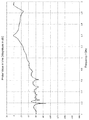
- FIG. 6 shows the result of analyzing the relationship between the frequency and the electric field intensity at the observation point outside the substrate when the GND through hole of FIG. 5 is not formed.
- FIG. 10 is an analysis of the case of FIG. 9 in the same manner as FIG. It is a figure which shows the analysis result of the electric field strength inside and outside a printed circuit board at the time of forming a GND through hole 2 times (2 rows) on the board outer periphery.
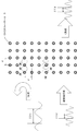
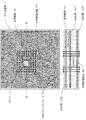
- FIG. 1 is a plan view and a cross-sectional view showing a printed circuit board 1 according to a first embodiment of the present invention.
- the cross-sectional view shows a cross section taken along the alternate long and short dash line AA ′ shown in the plan view.
- the cross section is not a straight line, but a cross section of the folded line is displayed so as to pass through a place including the power supply layer.
- the printed circuit board 1 is a multilayer printed circuit board, and a power supply layer 5 and a signal line 6 are formed with an insulating layer interposed therebetween.
- GND layers 41, 42, and 43 are formed as the entire substrate ground surface (solid ground) at least immediately below the component surface (the front surface side where the LSI 2 is located in FIG. 1) and directly above the solder surface (the back surface opposite to the component surface). . In FIG. 1, solder is not shown.
- the GND through holes 3 are arranged in a lattice pattern at intervals d (described later) on the entire surface of the substrate, and at least two GND layers (GND layers 41 and 42) are connected. In the present embodiment, the GND through hole 3 penetrates and connects all the GND layers 41, 42, and 43.
- the power supply lines 51, 52 and 53 are formed in the same layer in the printed circuit board 1 and are sandwiched between the GND layers 41 and 42.
- the power supply lines 51, 52, and 53 may be collectively referred to as the power supply layer 5.
- the GND through hole 3 may not be provided at a place where components such as the LSI 2 are mounted. There is a place where the GND through hole 3 penetrates the power supply layer 5. There is a gap (clearance) between the GND through hole 3 and the power supply layer 5 at this penetrating location, and this gap is filled with an insulator. (Description of operation) The mechanism of EMI radiation generated from the printed circuit board 1 will be described with reference to FIG.
- the substrate configuration applied in this embodiment is a power supply layer 5 (corresponding to power supply lines 51, 52, 53) sandwiched between GND layers 4 (corresponding to GND layers 41, 42).
- Electromagnetic waves are generated by changing the electric potential between the power supply layer 5 and the GND layer 3 so that the power supply current changes due to the operation of the IC (Integrated Circuit) and follows the power supply current. In FIG. 2, this is expressed by a noise source 90.
- the generated electromagnetic wave is propagated in all directions by turning the power source layer 5 to the GND layer 4 into a transmission path. Even in the region where the power supply layer 5 does not exist, the spread electromagnetic wave spreads, for example, between the GND layer 42 and the GND layer 43, another power supply layer-GND layer, or a power supply layer-power supply layer as a transmission path, and further spreads to the edge of the substrate.
- the electromagnetic wave propagated from the substrate end to the outside of the substrate is EMI radiation.
- FIG. 3 shows the electromagnetic wave blocking mechanism of the GND through hole 3.
- the GND through hole 3 ideally has an impedance of 0 and cannot pass through anything that becomes a node of electromagnetic waves.
- the impedance of the GND through hole 3 is not 0 and the traveling wave travels while being attenuated. .
- it is displayed as a noise traveling wave.
- an electromagnetic wave having a wavelength ⁇ 1 smaller than the lattice spacing d can propagate (transmit) through the lattice formed by the plurality of GND through holes 3.
- an electromagnetic wave having a wavelength ⁇ 2 longer than the grating interval d behaves as if it collides with a metal plate (impedance 0) and cannot be propagated through the grating and is reflected.
- an electromagnetic wave having a wavelength longer than ⁇ / 2 cannot pass through the grid of the GND through hole 3.
- the GND through hole 3 is a perfect conductor, it may be defined by ⁇ / 2.
- an analysis model for electromagnetic field analysis as shown in FIG. 4 was created, and the effects were confirmed by electromagnetic field analysis.
- the analysis model is as follows. Two GND layers 4 are formed on the printed circuit board 1, and the power supply layer 5 is sandwiched between the two GND layers 4, and noise is applied by a noise source 90 provided between the power supply layer 5 and the GND layer 4. Then, the electric field strength of the electromagnetic wave was analyzed.
- FIGS. 5 to 10 show the results of these analyses.
- 5 and 6 show that there is no GND through hole on the printed circuit board
- FIGS. 7 and 8 show that the GND through hole is arranged only on the outer periphery of the printed circuit board
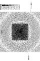
- FIGS. 9 and 10 show the condition that the GND through hole is arranged on the entire surface of the printed circuit board.
- the actual power supply layer has a long and narrow shape, but is analyzed here as a square in order to simplify the analysis.
- the scales in the upper right of FIGS. 5, 7, and 9 are scales from zero to minus, with the electric field strength decreasing toward minus and increasing the electric field strength toward zero.
- the unit is dB ⁇ V / m, but in the figure the plotted energy is plotted as a relative value with max (0 dB or 1). is doing.
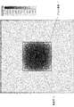
- FIG. 5 shows the analysis result of the electric field strength inside and outside the printed circuit board when no through hole is formed.
- the electric field from the power supply line leaks out of the substrate, and EMI radiation is generated.
- FIG. 6 is a diagram showing the relationship between the frequency and the electric field intensity at the observation point outside the substrate (indicated by a cross in the figure) in the case of FIG. 5 where no through hole is formed.
- the horizontal axis represents frequency (GHz), and the vertical axis represents electric field strength (dB ⁇ V / m) expressed in dB.
- the electric field strength exceeds -40 dB ⁇ V / m at 1 GHz or more and reaches 0 dB ⁇ V / m at the maximum.
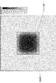
- FIG. 7 shows the analysis result of the electric field strength inside and outside the printed board 1 when only one layer (one row) of the GND through holes 3 is formed on the outer circumference of the printed board. Although improved from FIG. 5, it can be seen that EMI radiation is still generated outside the substrate 1.
- FIG. 8 shows an analysis of the case of FIG. 7 in the same manner as FIG. 6. However, although there is improvement, the electric field strength is still high and EMI radiation is generated outside the substrate.
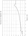
- FIG. 9 shows the analysis result of the electric field strength inside and outside the substrate when through holes are formed in the entire printed circuit board 1. It can be seen that EMI radiation to the outside of the substrate 1 is not seen, and that the electromagnetic wave stays around the power supply layer 5 even in the substrate 1.
- FIG. 10 is an analysis of the case of FIG. 9 in the same manner as in FIG. 6, but it can be seen that the electric field strength is less than ⁇ 80 dB ⁇ V / m over the entire measurement frequency, which is greatly improved. (Explanation of effect) Providing grid-like GND through holes on the entire surface of the substrate in this way makes it possible to suppress propagation of power supply noise around the printed circuit board and to suppress EMI radiation.
- the three power supply lines 51, 52 and 53 are all located in the same layer. However, even if some power supply lines are in different layers in the substrate or all power supply layers are in different layers in the substrate, the upper and lower sides of each power supply line are sandwiched between the GND layers, and the GND through hole 3 Just connect.
- the GND layers 42 and 43 and the GND through hole connecting them are provided from the power supply line 51. Suppresses external radiation of electromagnetic waves.
- the power supply line 53 is not located between the GND layers 41 and 42 but between the GND layer 41 and the surface of the LSI, a new GND layer is provided between the GND layer 41 and the surface.
- the lattice spacing d is 37.5 mm or less.
- Patent Document 4 Japanese Patent Laid-Open No. 11-220263
- the interval between through holes is described as 20 mm square (paragraph [0011]).
- Patent Document 4 it is necessary to make it relatively narrow as 20 mm, and in this embodiment, the difference that the lattice spacing may be relatively large as 37.5 mm is that Patent Document 4 aims to prevent EMI of both the power supply wiring and the signal wiring.
- the present embodiment is aimed at preventing EMI of the power supply line.
- the condition analyzed in FIG. 7 is that the GND through hole 3 is arranged only once around the outer periphery of the substrate, but EMI radiation is generated outside the substrate 1.
- EMI radiation is generated outside the substrate 1.
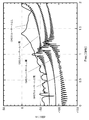
- FIG. 11 shows the analysis result of the electric field strength inside and outside the printed circuit board 1 when the GND through hole 3 is arranged twice, and FIG. 11 and 12, no EMI radiation to the outside of the substrate is seen.
- FIG. 13 shows the result of analyzing the relationship between the frequency and the electric field strength at the observation point outside the substrate in the case of FIGS. For comparison, a case where there is no GND through hole (FIGS. 5 and 6) and a case where there is only one round (FIGS. 7 and 8) are also shown.
- FIG. 14 is a plan view showing a third embodiment of the present invention and a sectional view taken along line BB ′. IC is omitted in the BB 'cross-sectional view.
- the propagation of power supply noise to the outside of the printed circuit board is suppressed.
- the propagation of power supply noise to the periphery of the power supply layer in the circuit board is suppressed.
- a power supply layer that is, an IC power supply wiring 54 runs in the printed circuit board 1 in the vertical direction in the figure below the IC 21.
- a GND layer 401 and a GND layer 402 are formed above and below the IC power supply wiring 54, and the GND through hole 3 is provided only around the IC power supply wiring 54 which is a source of power supply noise.
- the GND through hole 3 includes one that penetrates the IC power supply wiring 54 and one that is formed on both sides.
- three rows are formed on the left side of the IC power supply wiring 54 and four columns on the right side (three columns on the left and right sides of the IC 21), but at least two rows on both sides for the same reason as in the case of the outer periphery of the substrate described above. Just arrange them one by one.
- the GND layers 401 and 402 are both grounded. However, one of the two GND layers only needs to be formed in a region overlapping with the power supply layer and a region in which the GND through hole 3 is formed on both sides thereof.
- FIG. 15 is a plan view in that case and a sectional view taken along the line C-C ′. IC21 is omitted in the C-C 'sectional view.
- the GND layer 404 above the power supply layer is formed only in a region overlapping with the IC power supply wiring 54 in a plan view and a region where the GND through hole 3 is formed.
- a printed circuit board often has a plurality of power layers. If there are a plurality of power supply layers for which EMI radiation suppression is to be performed, the GND layer 404 is also formed for each power supply layer.
- the GND layer 403 disposed in the uppermost layer in FIG. 14 does not sandwich the power supply layer and is mainly used for impedance control of the signal wiring 61. If there is a power supply layer in the same layer as the signal layer, the GND layer 403 has an EMI suppression function.
- the GND layer and the GND through hole are formed above and below and around the power supply layer.
- the EMI suppression structure described in the second embodiment in which several GND through holes are formed on the outer periphery of the printed board may be combined.
- the GND through holes are arranged in parallel to the outer periphery of the printed circuit board or the power supply layer. However, they may be arranged in a zigzag manner, that is, staggered with respect to the outer periphery of the substrate. This arrangement can narrow the interval between the through holes. Therefore, the area of the region where the through hole is formed can be reduced.
- the present invention can be used for electronic circuit design and manufacture of information communication equipment and the like.
Abstract
Description
また特許文献5(特開2007-234500号公報)にはフレキシブル基板に形成した信号配線からの電磁波を遮断する技術が記載されている。複数の高速伝送路(信号配線)を配列するベース11の表面と裏面の両方にグランドパターンを形成し、この2つのグラウンドパターンを複数のスルーホール1sで接続している([0048]~[0053]段落、図1、3、5)。また複数のスルーホール1sの間隔は特定電磁波の1/2波長以下にすることで特定電磁波以上の波長を持つ電磁波を遮断することも記載されている([0063]段落)。 Patent Document 4 (Japanese Patent Laid-Open No. 11-220263) describes a printed wiring board that reduces electromagnetic noise. The printed
Patent Document 5 (Japanese Patent Laid-Open No. 2007-234500) describes a technique for blocking electromagnetic waves from signal wirings formed on a flexible substrate. A ground pattern is formed on both the front surface and the back surface of the base 11 on which a plurality of high-speed transmission lines (signal wirings) are arranged, and these two ground patterns are connected by a plurality of through holes 1s ([0048] to [0053]. ] Paragraph, Figures 1, 3, 5). It is also described that an electromagnetic wave having a wavelength equal to or greater than the specific electromagnetic wave is blocked by setting the interval between the plurality of through holes 1s to be equal to or less than ½ wavelength of the specific electromagnetic wave (paragraph [0063]).
図1~図5を用いて本発明の第1の実施形態を説明する。
(構成の説明)
図1は本発明の第1の実施形態のプリント基板1を示す平面図及び断面図である。断面図は平面図に示した一点鎖線A-A’の箇所の断面を示す。分かり易いように、断面は直線で切るのではなく電源層を含む場所を通るように、折り曲げた線における断面を表示している。プリント基板1は多層プリント基板であり、絶縁層を間に挟んで電源層5、信号線6が形成されている。
少なくとも部品面(図1ではLSI2のある表面側)直下と半田面(部品面と反対の裏面側)直上には、GND層41,42,43が基板全面グラウンド(ベタグラウンド)として形成されている。なお図1では半田の表示を省略している。基板全面に間隔d(後述)で格子状にGNDスルーホール3を配し、少なくとも2枚のGND層(GND層41,42)を接続する。本実施形態ではGNDスルーホール3はGND層41,42,43全てを貫通して接続している。電源線51,52,53はプリント基板1中の同層に形成されGND層41,42に挟まれている。以下電源線51,52,53をまとめて電源層5と呼称することがある。LSI2など部品が実装されている箇所ではGNDスルーホール3はなくてもよい。GNDスルーホール3が電源層5を貫通している箇所がある。この貫通箇所ではGNDスルーホール3と電源層5の間にギャップ(クリアランス)があり、絶縁体でこのギャップを埋めている。
(動作の説明)
図2を用いて、プリント基板1から発生するEMI放射のメカニズムを説明する。本実施形態で適用する基板構成はGND層4(GND層41,42に対応)で挟まれた電源層5(電源線51,52,53に対応)である。IC(Integrated Circuit)の動作により電源電流が変化しそれに追従するように電源層5-GND層3間電位の変化、すなわち電界が変化することにより、電磁波が発生する。図2ではこれを雑音源90で表現している。発生した電磁波は電源層5-GND層4間を伝送路と化し四方八方へと伝搬される。広がった電磁波は電源層5がない領域でも、例えばGND層42-GND層43間あるいは他の電源層-GND層間、あるいは、電源層-電源層間を伝送路と化し更に基板端まで広がっていく。基板端から基板外部へ伝搬した電磁波がEMI放射である。 (First embodiment)
A first embodiment of the present invention will be described with reference to FIGS.
(Description of configuration)
FIG. 1 is a plan view and a cross-sectional view showing a printed
GND layers 41, 42, and 43 are formed as the entire substrate ground surface (solid ground) at least immediately below the component surface (the front surface side where the
(Description of operation)
The mechanism of EMI radiation generated from the printed
d≦λ/4=C0/(4・fmax・√εr)・・・(式1)
となる条件を導くことが出来る。 Using this property, if a grating interval sufficiently smaller than the wavelength of the frequency to be suppressed as EMI is arranged, it becomes possible to suppress electromagnetic waves, and this is set to an interval smaller than a quarter wavelength (node to antinode). . Suppose that the upper limit of the frequency at which EMI is to be suppressed is f max , the relative permittivity of the printed circuit board is ε r , and the speed of light is C 0 , d ≦ λ / 4 = C 0 / (4 · f max · √ε r ) ( Formula 1)
The following conditions can be derived.
(効果の説明)
このように基板全面に格子状のGNDスルーホールを設けることで、電源雑音のプリント基板周囲への伝搬を抑制し、EMI放射を抑え込むことが可能となる。 FIG. 10 is an analysis of the case of FIG. 9 in the same manner as in FIG. 6, but it can be seen that the electric field strength is less than −80 dB · V / m over the entire measurement frequency, which is greatly improved.
(Explanation of effect)
Providing grid-like GND through holes on the entire surface of the substrate in this way makes it possible to suppress propagation of power supply noise around the printed circuit board and to suppress EMI radiation.
(第2の実施形態)
図7で解析した条件は基板外周にGNDスルーホール3を一周だけ配したものであるが、基板1外にEMI放射が生じている。GNDスルーホール3を二周、三周あるいはそれ以上配することで、基板全面に配さなくても電磁波の進行を妨げる効果がある。 As described above, if the relative permittivity of the printed circuit board is 4 and the maximum frequency fmax to be suppressed is 1 GHz and calculation is performed according to the above (Equation 1), the lattice spacing d is 37.5 mm or less. However, in Patent Document 4 (Japanese Patent Laid-Open No. 11-220263), in the case of electromagnetic noise of 1 GHz, the interval between through holes is described as 20 mm square (paragraph [0011]). In Patent Document 4, it is necessary to make it relatively narrow as 20 mm, and in this embodiment, the difference that the lattice spacing may be relatively large as 37.5 mm is that Patent Document 4 aims to prevent EMI of both the power supply wiring and the signal wiring. On the other hand, it is considered that the present embodiment is aimed at preventing EMI of the power supply line.
(Second Embodiment)
The condition analyzed in FIG. 7 is that the GND through hole 3 is arranged only once around the outer periphery of the substrate, but EMI radiation is generated outside the
(第3の実施形態)
図14は本発明の第3の実施形態を示す平面図とそのB-B’における断面図である。B-B’断面図ではICを省略している。第1,第2の実施形態ではプリント基板外への電源雑音の伝搬を抑制したが、本実施形態は基板内の電源層の周囲への電源雑音の伝搬を抑制するものである。 Also in Patent Document 4 (Japanese Patent Laid-Open No. 11-220263), an annular ground pattern is formed around the signal layer and the power supply layer, but it is formed only on the outer peripheral layer of the printed wiring board, and is outside the substrate. Is insufficient to suppress EMI emissions. The reason is that, as described in the explanation of (Formula 1), the through hole is not a perfect conductor but has a certain impedance. Increasing the number of through-hole rows two or three times can sufficiently contain electromagnetic waves.
(Third embodiment)
FIG. 14 is a plan view showing a third embodiment of the present invention and a sectional view taken along line BB ′. IC is omitted in the BB 'cross-sectional view. In the first and second embodiments, the propagation of power supply noise to the outside of the printed circuit board is suppressed. However, in the present embodiment, the propagation of power supply noise to the periphery of the power supply layer in the circuit board is suppressed.
(第4の実施形態)
前述の第3の実施形態では電源層の上下と周囲にGND層とGNDスルーホールを形成した。しかしそれに加えて、第2の実施形態で述べた、プリント基板外周に数周のGNDスルーホールを形成したEMI抑制構造を組合せても良い。このようにすると、基板内での電源層の周囲へのEMI放射を抑制でき、しかも仮に想定以上の強度のEMI放射によって電源層外にEMI放射されたとしても、プリント基板外へEMI放射されるのを抑制できる。
(第5の実施形態)
上述の第1~4の実施形態ではGNDスルーホールはプリント基板または電源層の外周と平行に配列しているが、基板外周に対してジグザグにつまり千鳥状に配列しても良い。このように配置するとスルーホールの間隔を狭くできる。そのためスルーホールを形成する領域の面積を狭くできる。 Note that the GND layer 403 disposed in the uppermost layer in FIG. 14 does not sandwich the power supply layer and is mainly used for impedance control of the signal wiring 61. If there is a power supply layer in the same layer as the signal layer, the GND layer 403 has an EMI suppression function.
(Fourth embodiment)
In the third embodiment described above, the GND layer and the GND through hole are formed above and below and around the power supply layer. However, in addition to that, the EMI suppression structure described in the second embodiment in which several GND through holes are formed on the outer periphery of the printed board may be combined. In this way, EMI radiation to the periphery of the power supply layer in the substrate can be suppressed, and even if EMI is emitted outside the power supply layer by EMI radiation having an intensity higher than expected, it is emitted to the outside of the printed circuit board. Can be suppressed.
(Fifth embodiment)
In the first to fourth embodiments described above, the GND through holes are arranged in parallel to the outer periphery of the printed circuit board or the power supply layer. However, they may be arranged in a zigzag manner, that is, staggered with respect to the outer periphery of the substrate. This arrangement can narrow the interval between the through holes. Therefore, the area of the region where the through hole is formed can be reduced.
2 LSI
3 GNDスルーホール
41、42、43、401、402、403、404 GND層
5 電源層
51、52、53 電源線
6 信号線
21 IC 1 Printed
3 GND through hole 41, 42, 43, 401, 402, 403, 404 GND layer 5 Power supply layer 51, 52, 53 Power supply line 6
Claims (9)
- プリント基板にグランド層を複数層設け、前記複数層のグランド層で電源層を挟み、少なくとも前記プリント基板の外周に前記複数層のグランド層を接続するスルーホールを設け、前記スルーホールは抑制したい電磁波の最大周波数に対応する波長に応じた間隔で設けることを特徴とするプリント基板。 A plurality of ground layers are provided on a printed circuit board, a power supply layer is sandwiched between the plurality of ground layers, and at least an outer periphery of the printed circuit board is provided with a through hole that connects the plurality of ground layers. A printed circuit board characterized by being provided at an interval corresponding to a wavelength corresponding to the maximum frequency of.
- プリント基板に設けた電源層の上下をグランド層で挟み、前記上下のグランド層を複数のスルーホールで接続し、前記スルーホールは前記電源層とその近傍に、抑制したい電磁波の最大周波数に対応する波長に応じた間隔を開けて設けることを特徴とするプリント基板。 The power supply layer provided on the printed circuit board is sandwiched between ground layers, and the upper and lower ground layers are connected by a plurality of through holes, and the through holes correspond to the maximum frequency of electromagnetic waves to be suppressed in the power supply layer and the vicinity thereof. A printed circuit board provided with an interval corresponding to a wavelength.
- 前記プリント基板の外周に前記複数層のグランド層を接続するスルーホールを設け、前記スルーホールは抑制したい電磁波の最大周波数に対応する波長に応じた間隔で設けた請求項2のプリント基板。 The printed circuit board according to claim 2, wherein through holes for connecting the plurality of ground layers are provided on an outer periphery of the printed circuit board, and the through holes are provided at intervals according to a wavelength corresponding to a maximum frequency of an electromagnetic wave to be suppressed.
- 前記間隔は前記抑制したい電磁波の最大周波数に対応する波長の1/4以下である請求項1から3のいずれか一項に記載のプリント基板。 The printed circuit board according to any one of claims 1 to 3, wherein the interval is ¼ or less of a wavelength corresponding to a maximum frequency of the electromagnetic wave to be suppressed.
- 前記スルーホールは少なくとも2列に設ける請求項1から4のいずれか一項に記載のプリント基板。 The printed circuit board according to any one of claims 1 to 4, wherein the through holes are provided in at least two rows.
- 前記複数層のグランド層は全面グランド層である請求項1から5のいずれか一項に記載のプリント基板。 The printed circuit board according to any one of claims 1 to 5, wherein the plurality of ground layers are whole ground layers.
- 前記上下のグランド層のどちらかは、前記電源層と重なる領域とその両側に前記スルーホールを形成する領域に形成されている請求項2または3に記載のプリント基板。 4. The printed circuit board according to claim 2, wherein one of the upper and lower ground layers is formed in a region overlapping with the power supply layer and a region in which the through hole is formed on both sides thereof.
- 前記電源層を複数備え、そのうちの少なくとも一つの電源層が他の電源層とは別の層に形成されている場合、前記別の層に形成された電源層についてもその上下をグランド層で挟む請求項1から7のいずれか1項に記載のプリント基板。 When a plurality of the power supply layers are provided and at least one of the power supply layers is formed in a layer different from the other power supply layers, the power supply layers formed in the other layers are also sandwiched between ground layers The printed circuit board according to any one of claims 1 to 7.
- 前記スルーホールは前記プリント基板または前記電源層の外周と平行または斜めに配列されている請求項1から8のいずれか一項に記載のプリント基板。 The printed circuit board according to any one of claims 1 to 8, wherein the through holes are arranged parallel to or obliquely with an outer periphery of the printed circuit board or the power supply layer.
Priority Applications (3)
| Application Number | Priority Date | Filing Date | Title |
|---|---|---|---|
| CN201680040215.3A CN107852829A (en) | 2015-07-08 | 2016-07-04 | Printed circuit board (PCB) |
| US15/737,876 US10375818B2 (en) | 2015-07-08 | 2016-07-04 | Printed board |
| JP2017527078A JPWO2017006552A1 (en) | 2015-07-08 | 2016-07-04 | Printed board |
Applications Claiming Priority (2)
| Application Number | Priority Date | Filing Date | Title |
|---|---|---|---|
| JP2015137091 | 2015-07-08 | ||
| JP2015-137091 | 2015-07-08 |
Publications (1)
| Publication Number | Publication Date |
|---|---|
| WO2017006552A1 true WO2017006552A1 (en) | 2017-01-12 |
Family
ID=57684965
Family Applications (1)
| Application Number | Title | Priority Date | Filing Date |
|---|---|---|---|
| PCT/JP2016/003168 WO2017006552A1 (en) | 2015-07-08 | 2016-07-04 | Printed board |
Country Status (4)
| Country | Link |
|---|---|
| US (1) | US10375818B2 (en) |
| JP (1) | JPWO2017006552A1 (en) |
| CN (1) | CN107852829A (en) |
| WO (1) | WO2017006552A1 (en) |
Cited By (3)
| Publication number | Priority date | Publication date | Assignee | Title |
|---|---|---|---|---|
| JP2019186332A (en) * | 2018-04-06 | 2019-10-24 | 三菱電機株式会社 | Print circuit board |
| JP2020202255A (en) * | 2019-06-07 | 2020-12-17 | 株式会社デンソー | Electronic apparatus |
| GB2618320A (en) * | 2022-04-28 | 2023-11-08 | Energy Res Lab Ltd | Electronic device with an embedded HFAC power distribution bus |
Families Citing this family (3)
| Publication number | Priority date | Publication date | Assignee | Title |
|---|---|---|---|---|
| CN213522492U (en) * | 2017-11-16 | 2021-06-22 | 株式会社村田制作所 | Resin multilayer substrate, electronic component, and mounting structure thereof |
| WO2019098011A1 (en) * | 2017-11-16 | 2019-05-23 | 株式会社村田製作所 | Resin multilayer substrate, electronic component, and mounting structure for electronic component |
| CN111586960B (en) | 2019-02-15 | 2021-09-14 | 华为技术有限公司 | Anti-interference circuit board and terminal |
Citations (4)
| Publication number | Priority date | Publication date | Assignee | Title |
|---|---|---|---|---|
| JP2001068801A (en) * | 1999-08-27 | 2001-03-16 | Sony Corp | Printed wiring board |
| JP2007088102A (en) * | 2005-09-20 | 2007-04-05 | Fuji Xerox Co Ltd | Printed circuit board |
| JP2009224566A (en) * | 2008-03-17 | 2009-10-01 | Nec Corp | Circuit and semiconductor circuit |
| WO2011111314A1 (en) * | 2010-03-08 | 2011-09-15 | 日本電気株式会社 | Wiring substrate, electronic device, and noise shielding method |
Family Cites Families (7)
| Publication number | Priority date | Publication date | Assignee | Title |
|---|---|---|---|---|
| JP2988421B2 (en) | 1997-03-24 | 1999-12-13 | 日本電気株式会社 | EMI suppression multilayer printed circuit board |
| JPH11220263A (en) | 1998-01-29 | 1999-08-10 | Oki Electric Ind Co Ltd | Printed wiring board |
| JP3784188B2 (en) | 1999-01-21 | 2006-06-07 | 京セラ株式会社 | Wiring board for mounting electronic components |
| JP3267274B2 (en) | 1999-08-13 | 2002-03-18 | 日本電気株式会社 | Multilayer printed circuit board |
| JP2003133814A (en) * | 2001-10-24 | 2003-05-09 | Kyocera Corp | Wiring board for high frequency |
| JP2007234500A (en) | 2006-03-03 | 2007-09-13 | Jst Mfg Co Ltd | High-speed transmission fpc and printed circuit board to be connected to the fpc |
| JP2013254759A (en) | 2012-06-05 | 2013-12-19 | Hitachi Ltd | Circuit substrate and electronic apparatus |
-
2016
- 2016-07-04 CN CN201680040215.3A patent/CN107852829A/en active Pending
- 2016-07-04 JP JP2017527078A patent/JPWO2017006552A1/en active Pending
- 2016-07-04 WO PCT/JP2016/003168 patent/WO2017006552A1/en active Application Filing
- 2016-07-04 US US15/737,876 patent/US10375818B2/en not_active Expired - Fee Related
Patent Citations (4)
| Publication number | Priority date | Publication date | Assignee | Title |
|---|---|---|---|---|
| JP2001068801A (en) * | 1999-08-27 | 2001-03-16 | Sony Corp | Printed wiring board |
| JP2007088102A (en) * | 2005-09-20 | 2007-04-05 | Fuji Xerox Co Ltd | Printed circuit board |
| JP2009224566A (en) * | 2008-03-17 | 2009-10-01 | Nec Corp | Circuit and semiconductor circuit |
| WO2011111314A1 (en) * | 2010-03-08 | 2011-09-15 | 日本電気株式会社 | Wiring substrate, electronic device, and noise shielding method |
Cited By (3)
| Publication number | Priority date | Publication date | Assignee | Title |
|---|---|---|---|---|
| JP2019186332A (en) * | 2018-04-06 | 2019-10-24 | 三菱電機株式会社 | Print circuit board |
| JP2020202255A (en) * | 2019-06-07 | 2020-12-17 | 株式会社デンソー | Electronic apparatus |
| GB2618320A (en) * | 2022-04-28 | 2023-11-08 | Energy Res Lab Ltd | Electronic device with an embedded HFAC power distribution bus |
Also Published As
| Publication number | Publication date |
|---|---|
| US20180235076A1 (en) | 2018-08-16 |
| JPWO2017006552A1 (en) | 2018-04-05 |
| CN107852829A (en) | 2018-03-27 |
| US10375818B2 (en) | 2019-08-06 |
Similar Documents
| Publication | Publication Date | Title |
|---|---|---|
| WO2017006552A1 (en) | Printed board | |
| JP4930590B2 (en) | Multilayer board | |
| US20130215587A1 (en) | Multilayer wiring board and electronic device | |
| US8779874B2 (en) | Waveguide structure and printed-circuit board | |
| US20120325537A1 (en) | Circuit board, electronic apparatus, and noise blocking method | |
| KR101072591B1 (en) | Electromagnetic interference noise reduction board using electromagnetic bandgap structure | |
| JP5725013B2 (en) | Structure, wiring board, and method of manufacturing wiring board | |
| WO2011111313A1 (en) | Electronic device, wiring substrate, and noise shielding method | |
| US9386689B2 (en) | Circuit board | |
| JP2008028218A (en) | Multilayer printed board | |
| JP6810001B2 (en) | High frequency transmission line | |
| JP5863801B2 (en) | Multi-plane printed wiring board for use in high frequency | |
| US8331105B2 (en) | Circuit board and semiconductor device | |
| JP2013539218A5 (en) | ||
| WO2017006553A1 (en) | Printed wiring board | |
| JP5353042B2 (en) | Printed wiring board | |
| WO2012042711A1 (en) | Wiring substrate and electronic device | |
| KR20110032601A (en) | Printed circuit board having electromagnetic bandgap structure | |
| JP6013296B2 (en) | High frequency transmission line | |
| KR101021552B1 (en) | Electromagnetic interference noise reduction board using electromagnetic bandgap structure | |
| JP5686624B2 (en) | High-frequency signal connection structure | |
| JP2019075444A (en) | Circuit board | |
| JP2005302799A (en) | Multilayered printed wiring board | |
| JP6131600B2 (en) | Printed circuit board having interlayer connection hole and arrangement method | |
| JP5673874B2 (en) | Periodic structure and wiring board |
Legal Events
| Date | Code | Title | Description |
|---|---|---|---|
| 121 | Ep: the epo has been informed by wipo that ep was designated in this application |
Ref document number: 16821028 Country of ref document: EP Kind code of ref document: A1 |
|
| ENP | Entry into the national phase |
Ref document number: 2017527078 Country of ref document: JP Kind code of ref document: A |
|
| WWE | Wipo information: entry into national phase |
Ref document number: 15737876 Country of ref document: US |
|
| NENP | Non-entry into the national phase |
Ref country code: DE |
|
| 122 | Ep: pct application non-entry in european phase |
Ref document number: 16821028 Country of ref document: EP Kind code of ref document: A1 |