WO2016208732A1 - 光導波路素子 - Google Patents
光導波路素子 Download PDFInfo
- Publication number
- WO2016208732A1 WO2016208732A1 PCT/JP2016/068864 JP2016068864W WO2016208732A1 WO 2016208732 A1 WO2016208732 A1 WO 2016208732A1 JP 2016068864 W JP2016068864 W JP 2016068864W WO 2016208732 A1 WO2016208732 A1 WO 2016208732A1
- Authority
- WO
- WIPO (PCT)
- Prior art keywords
- region
- core
- optical waveguide
- depletion layer
- waveguide device
- Prior art date
- Legal status (The legal status is an assumption and is not a legal conclusion. Google has not performed a legal analysis and makes no representation as to the accuracy of the status listed.)
- Ceased
Links
Images




Classifications
-
- G—PHYSICS
- G02—OPTICS
- G02F—OPTICAL DEVICES OR ARRANGEMENTS FOR THE CONTROL OF LIGHT BY MODIFICATION OF THE OPTICAL PROPERTIES OF THE MEDIA OF THE ELEMENTS INVOLVED THEREIN; NON-LINEAR OPTICS; FREQUENCY-CHANGING OF LIGHT; OPTICAL LOGIC ELEMENTS; OPTICAL ANALOGUE/DIGITAL CONVERTERS
- G02F1/00—Devices or arrangements for the control of the intensity, colour, phase, polarisation or direction of light arriving from an independent light source, e.g. switching, gating or modulating; Non-linear optics
- G02F1/01—Devices or arrangements for the control of the intensity, colour, phase, polarisation or direction of light arriving from an independent light source, e.g. switching, gating or modulating; Non-linear optics for the control of the intensity, phase, polarisation or colour
- G02F1/015—Devices or arrangements for the control of the intensity, colour, phase, polarisation or direction of light arriving from an independent light source, e.g. switching, gating or modulating; Non-linear optics for the control of the intensity, phase, polarisation or colour based on semiconductor elements having potential barriers, e.g. having a PN or PIN junction
- G02F1/025—Devices or arrangements for the control of the intensity, colour, phase, polarisation or direction of light arriving from an independent light source, e.g. switching, gating or modulating; Non-linear optics for the control of the intensity, phase, polarisation or colour based on semiconductor elements having potential barriers, e.g. having a PN or PIN junction in an optical waveguide structure
-
- G—PHYSICS
- G02—OPTICS
- G02F—OPTICAL DEVICES OR ARRANGEMENTS FOR THE CONTROL OF LIGHT BY MODIFICATION OF THE OPTICAL PROPERTIES OF THE MEDIA OF THE ELEMENTS INVOLVED THEREIN; NON-LINEAR OPTICS; FREQUENCY-CHANGING OF LIGHT; OPTICAL LOGIC ELEMENTS; OPTICAL ANALOGUE/DIGITAL CONVERTERS
- G02F1/00—Devices or arrangements for the control of the intensity, colour, phase, polarisation or direction of light arriving from an independent light source, e.g. switching, gating or modulating; Non-linear optics
- G02F1/01—Devices or arrangements for the control of the intensity, colour, phase, polarisation or direction of light arriving from an independent light source, e.g. switching, gating or modulating; Non-linear optics for the control of the intensity, phase, polarisation or colour
- G02F1/21—Devices or arrangements for the control of the intensity, colour, phase, polarisation or direction of light arriving from an independent light source, e.g. switching, gating or modulating; Non-linear optics for the control of the intensity, phase, polarisation or colour by interference
- G02F1/225—Devices or arrangements for the control of the intensity, colour, phase, polarisation or direction of light arriving from an independent light source, e.g. switching, gating or modulating; Non-linear optics for the control of the intensity, phase, polarisation or colour by interference in an optical waveguide structure
- G02F1/2257—Devices or arrangements for the control of the intensity, colour, phase, polarisation or direction of light arriving from an independent light source, e.g. switching, gating or modulating; Non-linear optics for the control of the intensity, phase, polarisation or colour by interference in an optical waveguide structure the optical waveguides being made of semiconducting material
-
- G—PHYSICS
- G02—OPTICS
- G02B—OPTICAL ELEMENTS, SYSTEMS OR APPARATUS
- G02B6/00—Light guides; Structural details of arrangements comprising light guides and other optical elements, e.g. couplings
- G02B6/10—Light guides; Structural details of arrangements comprising light guides and other optical elements, e.g. couplings of the optical waveguide type
- G02B6/12—Light guides; Structural details of arrangements comprising light guides and other optical elements, e.g. couplings of the optical waveguide type of the integrated circuit kind
- G02B2006/12083—Constructional arrangements
- G02B2006/12097—Ridge, rib or the like
-
- G—PHYSICS
- G02—OPTICS
- G02B—OPTICAL ELEMENTS, SYSTEMS OR APPARATUS
- G02B6/00—Light guides; Structural details of arrangements comprising light guides and other optical elements, e.g. couplings
- G02B6/10—Light guides; Structural details of arrangements comprising light guides and other optical elements, e.g. couplings of the optical waveguide type
- G02B6/12—Light guides; Structural details of arrangements comprising light guides and other optical elements, e.g. couplings of the optical waveguide type of the integrated circuit kind
- G02B6/122—Basic optical elements, e.g. light-guiding paths
- G02B6/1228—Tapered waveguides, e.g. integrated spot-size transformers
-
- G—PHYSICS
- G02—OPTICS
- G02F—OPTICAL DEVICES OR ARRANGEMENTS FOR THE CONTROL OF LIGHT BY MODIFICATION OF THE OPTICAL PROPERTIES OF THE MEDIA OF THE ELEMENTS INVOLVED THEREIN; NON-LINEAR OPTICS; FREQUENCY-CHANGING OF LIGHT; OPTICAL LOGIC ELEMENTS; OPTICAL ANALOGUE/DIGITAL CONVERTERS
- G02F1/00—Devices or arrangements for the control of the intensity, colour, phase, polarisation or direction of light arriving from an independent light source, e.g. switching, gating or modulating; Non-linear optics
- G02F1/01—Devices or arrangements for the control of the intensity, colour, phase, polarisation or direction of light arriving from an independent light source, e.g. switching, gating or modulating; Non-linear optics for the control of the intensity, phase, polarisation or colour
- G02F1/21—Devices or arrangements for the control of the intensity, colour, phase, polarisation or direction of light arriving from an independent light source, e.g. switching, gating or modulating; Non-linear optics for the control of the intensity, phase, polarisation or colour by interference
- G02F1/212—Mach-Zehnder type
-
- G—PHYSICS
- G02—OPTICS
- G02F—OPTICAL DEVICES OR ARRANGEMENTS FOR THE CONTROL OF LIGHT BY MODIFICATION OF THE OPTICAL PROPERTIES OF THE MEDIA OF THE ELEMENTS INVOLVED THEREIN; NON-LINEAR OPTICS; FREQUENCY-CHANGING OF LIGHT; OPTICAL LOGIC ELEMENTS; OPTICAL ANALOGUE/DIGITAL CONVERTERS
- G02F2201/00—Constructional arrangements not provided for in groups G02F1/00 - G02F7/00
- G02F2201/06—Constructional arrangements not provided for in groups G02F1/00 - G02F7/00 integrated waveguide
- G02F2201/063—Constructional arrangements not provided for in groups G02F1/00 - G02F7/00 integrated waveguide ridge; rib; strip loaded
Definitions
- the present invention relates to an optical waveguide element used in an optical integrated circuit.
- optical fiber communication device examples include an optical transport device used in long-distance / metro-type wavelength division multiplexing optical fiber communication, an optical interconnect device used in a data center, and the like.
- Patent Document 1 As an optical waveguide element used in an optical integrated circuit, Patent Document 1 includes a core having two silicon layers having different conductivity and a dielectric layer sandwiched between these two silicon layers. It is disclosed.
- the optical waveguide element described in Patent Document 1 employs a so-called SISCAP (silicon capacitor) structure in which a P-type silicon layer and an N-type silicon layer are used as two silicon layers, and silicon dioxide is used as a dielectric layer. Yes.
- SISCAP silicon capacitor
- Patent Document 1 discloses a SISCAP structure in which either a P-type silicon layer or an L-type silicon layer is bent into an L-shape. By adopting such a structure, the region where the carrier density changes can be extended not only in the direction parallel to the surface of the substrate but also in the direction perpendicular to the surface of the substrate.
- the region where the carrier density changes is limited to the central portion of the core where the two silicon layers overlap through the dielectric layer. It does not reach the entire region where the electric field of the guided light is distributed. Therefore, in order to increase the efficiency of refractive index modulation and reduce the drive voltage, it is necessary to (1) increase the doping density of each silicon layer or (2) increase the element length.
- the doping density of each silicon layer is increased, the carrier absorbs more light, resulting in a problem that the optical loss increases.
- the element length is increased, there arises a problem that the optical waveguide element is increased in size.
- the manufacturing process is complicated because the process of laminating the silicon layer on the dielectric layer is special among the manufacturing processes. Become.
- the optical waveguide element described in Patent Document 1 is difficult to manufacture, and it is also difficult to unify design rules with other optical circuits, so that it can be integrated with other optical circuits.
- the problem of difficulty arises. For example, in order to reduce optical loss and suppress variations in optical characteristics, a technique for reducing the variation of the laminated film thickness to 1 nm (nanometer) or less is required.
- the electric field of light guided through the core is distributed so as to spread in each silicon layer.
- the profile of the light guided through the core is asymmetric in the direction parallel to the substrate surface, and the light guided through the core has a transverse electric field (TE) component and a transverse magnetic field (TM) component as polarization components.
- TE transverse electric field
- TM transverse magnetic field
- the present invention has been made in view of the above problems, and an object of the present invention is to provide an optical waveguide element that can reduce optical loss, drive voltage, and size.
- an optical waveguide element of the present invention includes a protrusion and two non-flat members arranged so as to sandwich the protrusion along the first direction.
- a rib waveguide having a protruding portion is included as a core portion, and the core portion is disposed so as to overlap with each other in a second direction perpendicular to the first direction.
- a depletion layer extending from the projecting portion to at least one of the two non-projecting portions is formed between the first core region and the second core region. The position in the second direction of the depletion layer in each of the two non-projections is lower than the position in the second direction of the depletion layer in the protrusion.
- the guided light (light guided through the core portion) is localized in the projecting portion and the vicinity thereof, and the electric field distribution is the side wall (non-projecting) of the core portion. Does not reach the tip of the part). For this reason, even if the side wall of the core portion is rough, light scattering due to the roughness of the side wall is reduced, and as a result, light loss is reduced. Further, according to the above configuration, a depletion layer extending from the projecting portion to at least one of the two non-projecting portions is formed between the first core region and the second core region.
- the drive voltage can be reduced without increasing the optical loss and increasing the size of the optical waveguide device.
- the spatial overlap between the electric field profile of the guided light and the depletion layer can be increased in the entire region of the core portion.
- the efficiency of changing the carrier density is increased, and the drive voltage can be further reduced.
- an optical waveguide element of the present invention includes a protrusion and two non-flat members arranged so as to sandwich the protrusion along the first direction.
- a rib waveguide having a protruding portion is included as a core portion, and the core portion is disposed so as to overlap with each other in a second direction perpendicular to the first direction.
- a depletion layer extending from the projecting portion to at least one of the two non-projecting portions is formed between the first core region and the second core region.
- the height of the upper surface of the second core region in the projecting portion based on the height of the lower surface of the core portion is hr / 2 + hs / It is characterized by 2.
- the guided light (light guided through the core portion) is localized in the projecting portion and the vicinity thereof, and the electric field distribution is the side wall (non-projecting) of the core portion. Does not reach the tip of the part). For this reason, even if the side wall of the core portion is rough, light scattering due to the roughness of the side wall is reduced, and as a result, light loss is reduced. Further, according to the above configuration, a depletion layer extending from the projecting portion to at least one of the two non-projecting portions is formed between the first core region and the second core region.
- the drive voltage can be reduced without increasing the optical loss and increasing the size of the optical waveguide device.
- the overlap between the profile of the electric field of the guided light in the entire core portion and the depletion layer can be further increased, and the optical loss can be reduced.
- light loss can be reduced, drive voltage can be reduced, the size can be reduced, and the manufacturing process can be simplified.
- FIG. 1 It is sectional drawing of the optical waveguide element which concerns on Embodiment 1 of this invention. It is an electric field profile of the waveguide light in the cross section shown in FIG. (A) is a block diagram of a Mach-Zehnder interferometer, and (b) is a perspective view of an optical modulator equipped with a Mach-Zehnder interferometer. It is a top view of the optical waveguide device concerning Embodiment 2 of the present invention. It is an electric field profile of guided light in a depletion layer. It is another electric field profile of the guided light in a depletion layer.
- FIG. 1 is a sectional view of an optical waveguide device 100 according to the first embodiment of the present invention.
- the horizontal direction (first direction) and the vertical direction (second direction) are also shown.
- the optical waveguide device 100 includes a rib waveguide core (core part) 101, a substrate 102, a lower clad 103, and an upper clad 104.
- the lower clad 103 is formed on the substrate 102.
- the rib waveguide core 101 is formed on the lower clad 103.
- the upper clad 104 is formed on the rib waveguide core 101.
- the interface between the substrate 102 and the lower clad 103 is flat.
- the horizontal direction shown in FIG. 1 is a direction parallel to the interface, and the vertical direction shown in FIG. 1 is a direction orthogonal to the interface.
- the upper clad 104 side is on the upper side and the substrate 102 side is on the lower side.
- the rib waveguide core 101 includes a rib region (projecting portion) 101r formed at the center portion in the horizontal direction of the cross section shown in FIG. 1 and two slab regions arranged so as to sandwich the rib region 101r along the horizontal direction. (Non-projecting part) 101s.
- the width (length in the horizontal direction) of the rib region 101r is wr
- the thickness of the rib region 101r is hr
- the thickness of both slab regions 101s is hs.
- the region above the two slab regions 101s in the rib region 101r is referred to as a convex portion. That is, the rib region 101r is a region including a convex portion and a portion of the rib waveguide core 101 immediately below the convex portion.
- the rib waveguide core 101 is axisymmetric with respect to an axis (dotted line AA ′) extending in the vertical direction through the midpoint 101 rc in the horizontal direction of the rib region 101 r. Further, the convex side wall 101rs extends substantially in the vertical direction.
- Guided light (light guided through the rib waveguide core 101) is localized in the rib region 101r and its vicinity, and propagates in a direction (third direction) orthogonal to the cross section shown in FIG.
- the optical waveguide device 100 is designed so that the mode of guided light propagating through the rib waveguide core 101 is only the fundamental mode of the TE component.
- the wavelength of the guided light is in a wavelength band applied in optical communication and optical interconnect, and is in the range of 1200 nm to 1700 nm.
- the material of the rib waveguide core 101 and the substrate 102 is, for example, crystalline silicon.
- the material of the lower cladding 103 and the upper cladding 104 is, for example, silicon dioxide (silica). If the materials of the rib waveguide core 101, the substrate 102, the lower clad 103, and the upper clad 104 are as described above, the optical waveguide device 100 can be configured using an SOI (Silicon-on-insulator) wafer. .
- SOI Silicon-on-insulator
- a buried silica (BOX) layer can be used for the lower cladding 103.
- the upper cladding 104 can be formed by depositing silica on the rib waveguide core 101.
- hr is 220 nm.
- hs is preferably 150 nm or more.
- wr is 450 nm or more. It is preferable. If wr is 450 nm or more, it is also suitable for reducing the optical loss due to the roughness of the side wall 101rs.
- PN junction is formed in the rib waveguide core 101 in order to perform refractive index modulation based on carrier plasma dispersion caused by free carrier absorption. That is, in the optical waveguide device 100, the refractive index is changed by changing the carrier density at the PN junction.
- the inventor of the present application has newly devised a layout of a conductive region (including a depletion layer) in the rib waveguide core 101, and this new layout reduces optical loss, drive voltage, and modulation. Increased frequency.
- the rib waveguide core 101 includes a central region (a part of the first core region) 105, side regions (a part of the first core region) 106 and 107, and a connection region (a first core region). 108).
- the central region 105, the side regions 106 and 107, and the connection region 108 all have first conductivity, are electrically connected to each other, and form a first core region as a whole. .
- the central region 105 is provided immediately below the convex portion in the rib region 101r. All of the central region 105, the side region 106, and the side region 107 have their both sides extending in the vertical direction. The right side of the side region 106 is in contact with the left side of the central region 105, and the left side of the side region 107 is in contact with the right side of the central region 105. In each of the side regions 106 and 107, a part of the lower side of the corresponding central region 105 is in contact with a part of the upper side of the corresponding side region 106 and 107. Both side regions 106 and 107 have a thickness of approximately hs / 2.
- the left side of the side region 106 is in contact with an undoped region where dopant is not intentionally implanted.
- the right side of the side region 107 is in contact with the connection region 108.
- the thickness of the connection region 108 is hs.
- the width of the central region 105 is wr
- the width of the side region 106 is wd2
- the width of the side region 107 is wd1.
- the rib waveguide core 101 includes a central region (a part of the second core region) 109, side regions (a part of the second core region) 110 and 111, and a connection region (the second region). 112 (part of the core region).
- the central region 109, the side regions 110 and 111, and the connection region 112 all have the second conductivity, are electrically connected to each other, and form the second core region as a whole. .
- the central region 109 is partially included in the convex portion in the rib region 101 r and is provided immediately above the central region 105. All of the central region 109, the side region 110, and the side region 111 have their both sides extending in the vertical direction.
- the left side of the lateral region 110 is in contact with the right side of the central region 109, and the right side of the lateral region 111 is in contact with the left side of the central region 109.
- a part of the lower side of the corresponding central region 109 is in contact with a part of the upper side of the corresponding side region 110 and 111.
- Both the side regions 110 and 111 have a thickness of about hs / 2, which is equal to the thickness of the side regions 106 and 107.
- the right side of the side region 110 is in contact with an undoped region where dopant is not intentionally implanted.
- the left side portion of the side region 111 is in contact with the connection region 112.
- the thickness of the connection region 112 is hs.
- the width of the central region 109 is wr
- the width of the side region 110 is wd2
- the width of the side region 111 is wd1.
- the central region 109 does not reach the top of the convex portion.
- the central region 109 may be formed so as to reach the top of the convex portion.
- connection regions 108 and 112 and the rib region 101r are spaced apart from each other in the horizontal direction.
- the reason why such an arrangement is adopted is to reduce optical loss due to free carrier absorption.
- the distance from the midpoint 101 rc to the connection region 108 and the distance from the midpoint 101 rc to the connection region 112 are both the degree of light loss required in the optical waveguide device 100 and / or the operating frequency of the optical waveguide device 100. It can be set to an arbitrary length according to the above.
- the central region 105 and the central region 109 are arranged so as to overlap each other in the vertical direction.
- the side region 106 and the side region 111 are arranged so as to overlap each other in the vertical direction.
- the side region 107 and the side region 110 are arranged so as to overlap each other in the vertical direction.
- the first conductivity of the central region 105, the lateral regions 106 and 107, and the connection region 108 is P-type
- the conductivity of the N-type is N-type.
- a PN junction is formed by each region having the first conductivity (P-type) and each region having the second conductivity (N-type).
- a depletion layer 113 is formed at the boundary of the PN junction by applying a predetermined reverse bias voltage to the portion where the PN junction is formed. Depletion layer 113 is formed to extend from rib region 101r to both slab regions 101s.
- the vertical position of the PN junction between the lateral region 106 and the lateral region 111 is lower than the vertical position of the PN junction between the central region 105 and the central region 109.
- the vertical position of the PN junction between the lateral region 107 and the lateral region 110 is also lower than the vertical position of the PN junction between the central region 105 and the central region 109.
- the vertical position of the depletion layer 113 in both slab regions 101s is lower than the vertical position of the depletion layer 113 in the rib region 101r.
- the right side portion of the central region 105 and the left side portion of the side region 110 are arranged side by side in the horizontal direction, whereby a PN junction is formed. Yes.
- the left side portion of the central region 105 and the right side portion of the side region 111 are arranged side by side in the horizontal direction, thereby forming a PN junction.
- the depletion layer 113 is formed by applying the reverse bias voltage described above.
- Each of the depletion layer 113 formed between the central region 105 and the side region 110 and the depletion layer 113 formed between the central region 105 and the side region 111 has a corresponding rib region 101r and slab. It extends in the vertical direction at the boundary with the region 101s.
- FIG. 2 is an electric field profile of guided light in the cross section shown in FIG. As shown in FIG. 2, the electric field profile in the fundamental mode of the TE component of the guided light is also localized in both slab regions 101s.
- the electric field of the guided light is displayed on a linear scale.
- the profile is derived on the assumption that wr is 650 nm, hr is 220 nm, hs is 160 nm, and the wavelength of the guided light is 1550 nm.
- the depletion layer 113 is bent by 90 °.
- the bent portion may be rounded by being affected by the implantation profile of the dopant element during ion implantation and thermal diffusion during annealing. The rounding of the bent portion does not significantly affect the effect of the depletion layer 113.
- the horizontal spread (width) in the depletion layer 113 is substantially constant.
- the vertical extent (vertical position or thickness) of the depletion layer 113 changes at this time. According to the profile of the guided light localized in the rib waveguide core 101, the vertical spread is as small as approximately half or less of the horizontal spread. Therefore, it is easier to change the thickness of the depletion layer 113 than to change the width of the depletion layer 113 to improve the efficiency of refractive index modulation and reduce the drive voltage of the optical waveguide device 100.
- the optical waveguide device 100 has the following effects.
- each of the above-described regions having the first conductivity and each of the regions having the second conductivity are optimized so as to reduce the driving voltage. At this time, since the optical loss is reduced and the driving voltage is reduced by means different from the enlargement of the optical waveguide element 100, the enlargement of the optical waveguide element 100 can be avoided.
- the depletion layer 113 is extended to both slab regions 101s.
- the vertical position of the depletion layer 113 in both slab regions 101s is different from the vertical position of the depletion layer 113 in the rib region 101r (specifically, the vertical direction of the depletion layer 113 in the rib region 101r). Lower than position).
- the spatial overlap between the electric field profile of the guided light and the depletion layer 113 can be increased in the entire region of the rib waveguide core 101.
- the efficiency of changing the carrier density is increased, and the drive voltage can be further reduced.
- each of the connection regions 108 and 112 is hs, which is the thickness of the corresponding slab region 101s itself. This reduces series resistance (resistance from a low resistance region 114 to be described later to a boundary with the side region 107 and resistance from a low resistance region 115 to be described later to a boundary to the side region 111). For this reason, the RC time constant determined from this series resistance and the capacitance by the PN junction can be reduced. As a result, the optical waveguide device 100 can increase the modulation frequency.
- the electric field profile of the guided light is optimized by the cross-sectional shape of the rib waveguide core 101 shown in FIG.
- the shape of the depletion layer 113 is optimized by the arrangement of the regions having the first conductivity and the regions having the second conductivity, and the dopant distribution, independently of the electric field profile of the guided light. The Therefore, in the optical waveguide device 100, it is easy to reduce optical loss and drive voltage.
- wr is 650 nm
- hr is 220 nm
- hs is 160 nm.
- the values of wr, hr, and hs are not limited thereto. . That is, various dimensions of the optical waveguide device 100 can be changed as appropriate as long as the guided light propagating through the rib waveguide core 101 is ideally only in a single mode and the depletion layer 113 is appropriately formed. it can.
- the first conductivity is P-type and the second conductivity is N-type.
- the first conductivity is N-type and the second conductivity is P type may be sufficient.
- hs is preferably 100 nm or more.
- Each region having the first conductivity and each region having the second conductivity are formed by doping.
- a method for performing this doping for example, ion implantation can be employed.
- ion implantation can be employed.
- the distance that the ions enter the rib region 101r is approximately equal to the distance that the ions enter the two slab regions 101s. Therefore, the depletion layer 113 can be formed at a desired position by adjusting the vertical position of the depletion layer 113 between the upper surface of the rib region 101r and the upper surfaces of both slab regions 101s.
- the side region 106, the side region 107, the side region 110, and the side region 111 have the same thickness in the vertical direction.
- the vertical center of the depletion layer 113 in each slab region 101s coincides with the vertical center of the corresponding slab region 101s.
- the thickness of each of the side region 106, the side region 107, the side region 110, and the side region 111 varies within about 5%, the optical characteristics and electrical characteristics of the optical waveguide device 100 are not affected. Has little effect. Therefore, the side region 106, the side region 107, the side region 110, and the side region 111 can be regarded as having the same thickness within the range of variation.
- the vertical positions of the upper surface of the rib region 101r and the upper surfaces of both slab regions 101s are generally compatible with the formation of the PN junction by simultaneously performing ion implantation into the rib region 101r and both slab regions 101s.
- ion implantation the manufacturing process of the optical waveguide device 100 can be simplified, and the manufacturing accuracy of the optical waveguide device 100 is improved. Therefore, it becomes easy to integrate the optical waveguide device 100 together with other circuits.
- the vertical center of the depletion layer 113 in the rib region 101r and the vertical center of the depletion layer 113 in each slab region 101s are individually set. Think about when you need to adjust to.
- ion implantation for the rib region 101r and ion implantation for each slab region 101s may be performed separately.
- annealing treatment may be performed in each ion implantation step as necessary.
- the first conductivity and the second conductivity may be a combination of P-type and N-type, or may be a combination of N-type and P-type. . Which of these combinations is adopted may be determined according to characteristics such as the diffusion coefficient of the element to be implanted.
- the central region 105, the side region 106, and the side region 107 can be formed by one ion implantation by self-alignment.
- the material of the rib waveguide core 101 is crystalline silicon, for example, boron can be used as the P-type ions to be implanted.
- the central region 105 is formed in the rib region 101r, and the side regions 106 and 107 are formed in the lower half of the corresponding slab region 101s.
- connection region 108 in order to form the connection region 108, two-stage ion implantation is required.
- the first-stage ion implantation is common to the above-described self-alignment ion implantation.
- the connection region 108 is formed substantially in the lower half of the right slab region 101s.
- the ion implantation region is limited to a direction perpendicular to the connection region 108 by using an optical mask or the like, the acceleration voltage is reduced, and the connection region 108 is roughly aligned with the right slab region 101s. Form in the upper half.
- ion implantation is performed with increasing the dose amount in the region including the upper surface in the connection region 108, and the low resistance region 114 having the first conductivity is formed in the connection region 108 in the slab region 101s. To do.
- the optical waveguide device 100 includes vertical through-wirings 116 and 117 provided in the horizontal direction with respect to the upper clad 104, a surface electrode 118 provided above the vertical through-wiring 116, and the vertical through-wiring 117. And a surface electrode 119 provided.
- one end of the vertical through wiring 116 is connected to the upper surface of the low resistance region 114, and the surface electrode 118 is connected to the other end of the vertical through wiring 116.
- the central region 109, the side region 110, and the side region 111 can be formed by self-alignment.
- arsenic can be used as the N-type ions to be implanted.
- the central region 109 is formed above the central region 105 in the rib region 101r, and the side regions 110 and 111 are formed in approximately the upper half of the corresponding slab region 101s. .
- connection region 112 two-stage ion implantation is required as in the formation of the connection region 108.
- the first-stage ion implantation is common to the above-described self-alignment ion implantation.
- the connection region 112 is formed substantially in the lower half of the left slab region 101s.
- an ion implantation region is limited to a direction perpendicular to the connection region 112 by using an optical mask or the like, the acceleration voltage is reduced, and the connection region 112 is substantially the same as the left slab region 101s. Form in the upper half.
- connection region 112 ion implantation is performed with increasing the dose amount in a region including the upper surface in the connection region 112, and a low resistance region 115 having second conductivity is formed inside the connection region 112 in the slab region 101s. To do.
- one end of the vertical through wiring 117 is connected to the upper surface of the low resistance region 115, and the surface electrode 119 is connected to the other end of the vertical through wiring 117.
- the surface electrodes 118 and 119 are part of a high-frequency electrode.
- the material of the vertical through wiring 116, the vertical through wiring 117, the surface electrode 118, and the surface electrode 119 is, for example, metallic aluminum or metallic copper.
- a high-frequency electric signal is applied to at least one of the surface electrodes 118 and 119 via a capacitor (not shown) that functions as a DC (Direct current) block.
- a capacitor not shown
- high-speed optical modulation is possible by applying a DC reverse bias voltage through an inductor (not shown) functioning as an AC (Alternating Current) block.
- the width of the depletion layer 113 is set to a value that covers substantially all of the spread of the guided light in the horizontal direction.
- wd2 becomes about 300 nm or more.
- the both ends of the depletion layer 113 in the horizontal direction are points where the electric field by the guided light attenuates by about 13 dB with respect to the peak value of the electric field by the guided light in the rib waveguide core 101. It is preferable to be located at.
- the end of the depletion layer 113 in the horizontal direction.
- Wd1 is preferably 700 nm to 1200 nm.
- the horizontal distance between the midpoint 101 rc and the connection region 108 and the horizontal distance between the midpoint 101 rc and the connection region 112 are both approximately 1000 nm to 1500 nm.
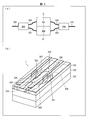
- FIG. 3A is a block diagram of the Mach-Zehnder interferometer
- FIG. 3B is a perspective view of the optical modulator 1 including the Mach-Zehnder interferometer.
- Mach-Zehnder interferometers are widely used in optical modulators for optical communications because they have advantages such as being less susceptible to external noise and having high stability of modulation operation against temperature changes. .
- the Mach-Zehnder interferometer shown in FIG. 3A has the following configuration.
- the incident end of the incident side waveguide 305 is used for optical coupling with an incident side optical fiber (not shown).
- the exit end of the incident-side waveguide 305 is connected to the incident end of the optical branching unit 303.
- One outgoing end of the optical branching section 303 is connected to the incident end of the arm waveguide 306, and the other outgoing end of the optical branching section 303 is connected to the incident end of the arm waveguide 307.
- the exit end of the arm waveguide 306 is connected to the entrance end of the phase modulation unit 301.
- the exit end of the arm waveguide 307 is connected to the entrance end of the phase modulation unit 302.
- the exit end of the phase modulation unit 301 is connected to the entrance end of the arm waveguide 308.
- the exit end of the phase modulation unit 302 is connected to the entrance end of the arm waveguide 309.
- the exit end of the arm waveguide 308 is connected to one incident end of the optical multiplexing unit 304.
- the exit end of the arm waveguide 309 is connected to the other entrance end of the optical multiplexing unit 304.
- the exit end of the optical multiplexing unit 304 is connected to the entrance end of the exit side waveguide 310.
- the exit end of the exit side waveguide 310 is used for optical coupling with an exit side optical fiber (not shown).
- the arm waveguide 306, the phase modulation unit 301, and the arm waveguide 308 form a first arm unit
- the arm waveguide 307, the phase modulation unit 302, and the arm waveguide 309 form a second arm unit. Is forming.
- Each of the phase modulation section 301 and the phase modulation section 302 includes one optical waveguide device 100 shown in FIG. More specifically, the DD ′ cross section shown in FIG. 3A is equal to the cross section shown in FIG.
- the optical modulator 1 is an optical modulator that can be used for optical communication, and applies a modulation electric field corresponding to a modulation signal to a PN junction based on silicon (Si).
- This is a silicon light modulator that modulates incident light.
- the optical modulator 1 has a layered structure in which a substrate 102, a lower clad 103, and an upper clad 104 are laminated in that order.
- each member shown in FIG. 3A is provided between the lower clad 103 and the upper clad 104 as an optical waveguide constituting the Mach-Zehnder interferometer.
- the incident side waveguide 305, the arm waveguide 306, the arm waveguide 307, the arm waveguide 308, the arm waveguide 309, and the emission side waveguide 310 are rectangular waveguides having a rectangular core.
- the material of the rectangular core is, for example, crystalline silicon.
- the width and thickness of this rectangular core are wi and hr, respectively.
- wi is 500 nm
- the fundamental mode of the TE component is waveguided light.
- 310 is propagated.
- the optical branching unit 303 and the optical multiplexing unit 304 are configured by, for example, a 1 ⁇ 2 multimode interferometer and a 2 ⁇ 2 multimode interferometer, respectively.
- the thickness of each of these multimode interferometers is hr.
- Each of these members is configured using an SOI wafer.
- phase modulators 301 and 302 By inputting a high-frequency electric signal to at least one of the phase modulators 301 and 302, light intensity modulation can be performed.
- optical phase modulation can be performed by inputting mutually complementary high-frequency electrical signals to the phase modulation units 301 and 302 and performing push-pull driving.
- the symbol rate of the high frequency electrical signal is 10 Gbaud or higher.
- the width of the rib region 101 r and both slab regions 101 s in the optical waveguide device 100 portion is avoided in order to avoid an increase in optical loss and higher-order mode excitation. It is preferable to form a tapered shape that gradually changes. The same applies to the connection between the arm waveguide 307, the phase modulation unit 302, and the arm waveguide 309.
- FIG. 4 is a top view of the optical waveguide device 100 ′ according to the second embodiment of the present invention.
- the horizontal direction and the guided light propagation direction are shown together.
- the guided light propagation direction is a direction perpendicular to both the horizontal direction and the vertical direction (see FIG. 1).
- the optical waveguide device 100 ′ is the same as the optical waveguide device 100 shown in FIG. 1 except that the horizontal width of the rib region 101r and both slab regions 101s varies depending on the position in the guided light propagation direction. It has a configuration.
- the cross section DD ′ of the optical waveguide device 100 ′ shown in FIG. 4 is equal to the cross section of the optical waveguide device 100 shown in FIG.
- the optical waveguide device 100 ′ On the incident end side in the phase modulation unit 301, the optical waveguide device 100 ′ has a first taper portion 401 along the guided light propagation direction for connection with the arm waveguide 306.
- the first taper portion 401 has a tapered shape such that the width of both slab regions 101s along the horizontal direction becomes smaller as closer to the guided light incident side, and the width of both slab regions 101s at the incident end is as follows. It is almost zero.
- the horizontal width of the rib region 101 r in the first taper portion 401 is wi in the entire area of the first taper portion 401.
- the cross-sectional shape of the rib region 101 r in the first taper portion 401 is substantially the same as the cross-sectional shape of the rectangular core of the arm waveguide 306.
- the length la of the first tapered portion 401 in the guided light propagation direction is 30 ⁇ m (micrometer).
- the outgoing end of the first tapered portion 401 is connected to the incident end of the second tapered portion 402. That is, the second taper portion 402 is disposed adjacent to the end portion of the first taper portion 401 on the guided light emission side.
- the second tapered portion 402 has a tapered shape such that the closer to the guided light incident side, the smaller the width of the rib region 101r along the horizontal direction.
- the horizontal width of the rib region 101r at the incident end of the second tapered portion 402 is the same wi as the same width of the first tapered portion 401, and the horizontal width of the rib region 101r at the outgoing end of the second tapered portion 402 is wr.
- the length lb of the second tapered portion 402 in the guided light propagation direction is 30 ⁇ m.
- both la and lb are not limited to 30 ⁇ m, and may be as short as possible to prevent an increase in optical loss and higher-order mode excitation in the optical waveguide device 100 ′.
- the width (wi) of the rectangular core of the arm waveguide 306 is larger than 500 nm, there is a high possibility that higher-order mode excitation occurs.
- higher-order mode excitation occurs, the extinction ratio in light intensity modulation or the Q value in optical phase modulation decreases.
- regions 101s is expanded gradually.
- the horizontal width of the rib region 101r is gradually increased from wi (500 nm) to wr (650 nm). In this way, it is possible to configure an optical modulation element with a small optical loss and a high extinction ratio or Q value. Further, when the optical waveguide device 100 ′ is used as the phase modulation unit 301 of the Mach-Zehnder interferometer, it is possible to prevent an increase in optical loss and high-order mode excitation.
- connection between the arm waveguide 306 and the phase modulation unit 301 has been described as an example.
- connection between the arm waveguide 307 and the phase modulation unit 302 also includes the configuration of the optical waveguide element 100 ′. Can be applied.
- the configuration of the optical waveguide element 100 ′ can also be applied to the connection between the phase modulation unit 301 and the arm waveguide 308 and the connection between the phase modulation unit 302 and the arm waveguide 309.
- the input end and the output end may be reversed with respect to the connection example between the arm waveguide 306 and the phase modulation unit 301.
- the length of the phase modulation units 301 and 302 in the guided light propagation direction is, for example, 3 mm (millimeters).
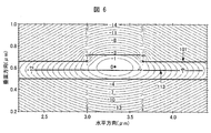
- FIGS. 5 and 6 are electric field profiles of guided light in the depletion layer 113, respectively.
- an example of the profile of the depletion layer 113 is displayed together with contour lines of the electric field absolute value of the guided light (TE mode) and the outline of the rib waveguide core 101.
- the contour lines are standardized to 1 in the peak of the electric field absolute value of the guided light, and the electric field absolute values are drawn at 1 dB intervals.
- the point indicated as “0” indicates the peak (0 dB) of the electric field absolute value.
- the depletion layer 113 having the profile shown in FIG. 5 maximizes the overlap between the waveguide optical field profile and the depletion layer 113, thereby maximizing the effect of reducing the driving voltage of the optical waveguide device 100.
- the positions of both ends in the horizontal direction of the depletion layer 113 are approximately at points where the absolute value of the guided light electric field is attenuated by 13 dB from the peak value.
- the spread in the horizontal direction of the depletion layer 113 is about 1 ⁇ m on both sides in the horizontal direction around the position of the peak value.
- the electric capacity due to the above-described PN junction is about 12 pF. Since the series electric resistance connected to the PN junction is about 8 ohms in total for both sides of the PN junction, the RC time constant is about 100 ps.
- the RC time constant is required to be approximately 100 ps or less, and the electric capacity by this PN junction is preferably 12 pF. Since the capacitance is substantially proportional to the horizontal spread of the depletion layer 113, the positions of both ends of the depletion layer 113 in the horizontal direction are more depleted than the point where the absolute value of the guided light electric field is attenuated by about 13 dB from the peak value. It is preferable to exist on the center side of 113. The same can be said even when the profile of the depletion layer 113 is different from that shown in FIG.
- the vertical position (height) of the depletion layer 113 is a half of the thickness of both slab regions 101 s with respect to the lower surface of the rib waveguide core 101, that is, hs. / 2. This maximizes the overlap between the electric field profile of the guided light and the depletion layer 113 in both slab regions 101s. Therefore, the height of the depletion layer 113 in both slab regions 101s with respect to the height of the lower surface of the rib waveguide core 101 is preferably hs / 2 (where hs is the thickness of both slab regions 101s). .
- the lower surface of both the slab regions 101s and the lower surface of the rib region 101r have the same vertical position, and the lower surface of the rib waveguide core 101 is flat.
- the side region 106 and the side region 107 are formed in the lower half, and the side region 110 and the side region 111 are formed in the upper half. Resistance has been reduced.
- the thickness of the side region 106, the side region 107, the side region 110, and the side region 111 is hs / 2.
- the height of the depletion layer 113 in the rib region 101r with reference to the height of the lower surface of the rib waveguide core 101. Is hr / 2.
- the central region 105 thicker than the side regions 106 and 107 and the central region 109 thicker than the side regions 110 and 111 can be formed from the viewpoint of reducing the series electric resistance.
- the thickness of the central region 105 is the same as that of the side regions 106 and 107
- the thickness of the central region 109 is the same as that of the side regions 110 and 111.
- the height of the lower surface of the rib waveguide core 101 is hr / 2 ⁇ hs / 2, and the height of the upper surface of the central region 109 in the rib region 101r.
- the height is hr / 2 + hs / 2.
- rib region 101r has an undoped region in which P-type or N-type dopant is not intentionally implanted immediately above central regions 105 and 109 and at least one of right under central regions 105 and 109. Yes.
- the undoped region there may be a case where the dopant distribution is slightly caused by diffusion, but this case hardly affects the optical characteristics of the optical waveguide device 100.
- the rib waveguide core 101 is formed by optical lithography and dry etching, and then ion implantation is separately performed in the rib region 101r and both slab regions 101s. Either ion implantation in the rib region 101r or ion implantation in both slab regions 101s may be performed first. If the series resistance needs to be reduced, the thickness of the central regions 105 and 109 may be increased.
- the depletion layer 113 extends in the vertical direction at the boundary between the rib region 101r and both slab regions 101s.
- at least one of the electrical resistances associated with the connection between the central region 109 and the side region 111 is increased. This may increase the series electric resistance.
- the depletion layer 113 may be formed in a straight line in the horizontal direction (so that there is no portion extending in the vertical direction) as shown in FIG.
- the height of the depletion layer 113 in the rib region 101r is set to hs / 2, which is the same as the height of the depletion layer 113 in both slab regions 101s.
- the height of the upper surface of the central region 109 in the rib region 101r is hs.
- ion implantation is simultaneously performed on the rib region 101r and both slab regions 101s.
- the thickness of the rib waveguide core 101 at the position where it will later become both slab regions 101s is equal to the thickness of the rib region 101r and is hr.
- the rib waveguide core 101 is formed by optical lithography and dry etching, and the height of both slab regions 101s becomes hs.
- the rib waveguide core 101 is formed by optical lithography and dry etching before ion implantation, and ion implantation is simultaneously performed on the rib region 101r and both slab regions 101s in order to simplify the ion implantation process.
- the depletion layer 113 is formed.
- the profile of the depletion layer 113 is different from that shown in FIGS.
- the vertical position of the depletion layer 113 is hr-hs / 2
- the height of the lower surface of the central region 105 is hr-hs.
- the first priority is to reduce the driving voltage by increasing the overlap between the electric field profile of the guided light and the depletion layer 113, high-speed refractive index modulation by reducing the series electrical resistance, and simplifying the processing process for integration.
- the profile of the depletion layer 113 is different.
- the vertical position (height) of the depletion layer 113 in the rib region 101r is measured from the height of the lower surface of the rib waveguide core 101 in the direction away from the substrate 102 (upward). It is in the range of hs / 2 or more and hr-hs / 2 or less.
- hs is the thickness of both slab regions 101s
- hr is the thickness of the rib region 101r.
- the optical waveguide element 100 has been described above, the same applies to the optical waveguide element 100 ′.
- the above description is valid even if the first conductivity / second conductivity is a combination of P-type and N-type, and also a combination of N-type and P-type.
- the optical waveguide element according to the present invention includes a rib guide having a protruding portion and two non-projecting portions that are arranged so as to sandwich the protruding portion along the first direction.
- a core is included as a core portion, and the core portion includes a first core region and a second core region that form a PN junction and are stacked in a second direction perpendicular to the first direction.
- a depletion layer extending from the projecting portion to at least one of the two non-projecting portions may be formed between the first core region and the second core region.
- the guided light (light guided through the core portion) is localized in the projecting portion and the vicinity thereof, and the electric field distribution is the side wall (non-projecting) of the core portion. Does not reach the tip of the part). For this reason, even if the side wall of the core portion is rough, light scattering due to the roughness of the side wall is reduced, and as a result, light loss is reduced. Further, according to the above configuration, a depletion layer extending from the projecting portion to at least one of the two non-projecting portions is formed between the first core region and the second core region.
- the drive voltage can be reduced without increasing the optical loss and increasing the size of the optical waveguide device.
- the depletion layer may extend from the protruding portion to both of the two non-projecting portions.
- the spatial overlap between the electric field profile of the guided light and the depletion layer can be increased in the non-projecting portion.
- the efficiency of changing the carrier density is increased, and the drive voltage can be further reduced.
- the optical waveguide element of the present invention has an end in the first direction of the depletion layer so that the attenuation factor of the electric field of the guided light is within 13 dB with respect to the electric field peak value of the guided light in the core portion. May be defined.
- the thickness of the first core region in the second direction and the thickness of the second core region in the second direction are equal in at least one non-projecting portion. Good.
- the position in the second direction of the depletion layer in the at least one non-projecting part may be different from the position in the second direction of the depletion layer in the projecting part.
- the position of the depletion layer in the second direction of the depletion layer in at least one non-projection may be lower than the position of the depletion layer in the projection in the second direction.
- the optical waveguide element has a tapered shape such that the width of each non-projecting portion along the first direction becomes smaller as it is closer to one of the incident side and the outgoing side of light.
- a first taper portion having the first taper portion and the other end portion on the light incident side and the light emission side of the first taper portion, the first direction being closer to one of the light incident side and the light emission side.
- a second tapered portion having a tapered shape such that the width of the projecting portion along the width is reduced.
- the optical waveguide element of the present invention when used as a phase modulation unit of each arm of a Mach-Zehnder interferometer, it is possible to prevent an increase in optical loss and high-order mode excitation. it can.
- the height of the depletion layer in the at least one non-projecting portion with respect to the height in the second direction with respect to the height of the lower surface of the core portion is hs / 2 (however, Hs: thickness of the non-projecting portion).
- the overlap between the profile of the electric field of the guided light at the non-projecting portion and the depletion layer is maximized.
- the height of the depletion layer in the projecting portion is greater than or equal to hs / 2 and hr ⁇ with respect to the height of the lower surface of the core portion in the second direction. It may be hs / 2 or less (where hs is the thickness of at least one non-projecting portion, and hr is the thickness of the projecting portion).
- the overlap between the profile of the electric field of the guided light at the protrusion and the depletion layer is maximized.
- the protrusion in the projecting portion with respect to the height of the lower surface of the core portion in the second direction is used.
- the height of the lower surface of the first core region is hr / 2 ⁇ hs / 2
- the height of the upper surface of the second core region in the protruding portion is based on the height of the lower surface of the core portion. Hr / 2 + hs / 2.
- the protrusion is at least one of the first core region and the second core region, and the first core region and the second core region. It may have an undoped region where dopant is not intentionally implanted.
- the overlap between the profile of the electric field of the guided light and the depletion layer in the entire core portion can be further increased, and the optical loss can be reduced.
- the present invention can be used for an optical waveguide device used in an optical integrated circuit.
Landscapes
- Physics & Mathematics (AREA)
- Nonlinear Science (AREA)
- General Physics & Mathematics (AREA)
- Optics & Photonics (AREA)
- Optical Integrated Circuits (AREA)
- Optical Modulation, Optical Deflection, Nonlinear Optics, Optical Demodulation, Optical Logic Elements (AREA)
Abstract
光損失の低減、駆動電圧の低減、小型化、および製造工程の簡易化を可能とする。リブ領域(101r)と、両スラブ領域(101s)とを有しているリブ導波路コア(101)を備えており、リブ領域(101r)から2つのスラブ領域(101s)にまで延伸する空乏層(113)が形成される。
Description
本発明は、光集積回路に用いられる光導波路素子に関する。
近年、光導波路素子を含む光集積回路を、光ファイバ通信用の各種デバイスに応用することが検討されている。光ファイバ通信用のデバイスとしては、例えば、長距離・メトロ系の波長多重光ファイバ通信で用いられる光トランスポート装置や、データセンタ等で用いられる光インタコネクト装置等が挙げられる。
光集積回路に用いられる光導波路素子として、特許文献1には、相異なる導電性を有する2つのシリコン層と、これら2つのシリコン層に挟まれた誘電体層とを有するコアを備えたものが開示されている。特許文献1に記載の光導波路素子においては、2つのシリコン層としてP型シリコン層およびN型シリコン層を用い、誘電体層として二酸化シリコンを用いた、いわゆるSISCAP(シリコンキャパシタ)構造が採用されている。
特許文献1に記載の光導波路素子では、各シリコン層の側壁(基板の面に沿う方向における該シリコン層の終端)とクラッドとの屈折率の差により光の閉じ込めが実現されており、コアを導波する光の電界は、上記2つのシリコン層と上記誘電体層とに拡がるように分布する。このため、上記2つのシリコン層のキャリア密度を変化させることにより、上記誘電体層を介して上記2つのシリコン層が重なりあったコアの中央部分において、コアを導波する光に対する屈折率を変化させることができる。
また、特許文献1には、P型シリコン層またはL型シリコン層のいずれかをL字型に折り曲げたSISCAP構造が開示されている。このような構造を採用することにより、キャリア密度が変化する領域を、基板の面に対して平行な方向のみならず、基板の面に対して垂直な方向にも延設することができる。
特許文献1に記載の光導波路素子では、上述したように、各シリコン層の側壁(基板の面に沿う方向における該シリコン層の終端)とクラッドとの屈折率の差により光の閉じ込めが実現される。このため、各シリコン層の側壁が荒れていると、その側壁にてコアを導波する光が散乱されてしまい、光損失が大きくなるという問題が発生する。
また、特許文献1に記載の光導波路素子では、上述したように、キャリア密度が変化する領域が、誘電体層を介して2つのシリコン層が重なりあったコアの中央部分に限定され、コアを導波する光の電界が分布する領域全体には及ばない。したがって、屈折率変調の効率を高めて駆動電圧を低下させるためには、(1)各シリコン層のドーピング密度を高くするか、または、(2)素子長を長くする必要がある。各シリコン層のドーピング密度を高くした場合、キャリアがより多くの光を吸収してしまい、結果、光損失が大きくなるという問題が発生する。一方、素子長を長くした場合、光導波路素子の大型化を招くという問題が発生する。
さらに、副次的な問題として、特許文献1に記載の光導波路素子では、その製造工程のうち、誘電体層にシリコン層を積層する工程が特殊なものとなるため、その製造工程が複雑となる。この結果、特許文献1に記載の光導波路素子は、その製造が難しく、また、他の光回路との間でデザインルールを統一することも困難であるため、他の光回路と共に集積することが困難であるという問題が発生する。例えば、光損失低減および光学特性のバラつきを抑えるため、積層膜厚の変動を1nm(ナノメートル)以下に低減する技術が必要になる。
さらに、別の副次的な問題として、特許文献1に記載の光導波路素子では、各シリコン層に拡がるように、コアを導波する光の電界が分布する。このため、コアを導波する光のプロファイルは、基板面と平行な方向において非対称となり、コアを導波する光は、横電界(TE)成分と横磁界(TM)成分とを偏波成分として含むこととなる。この結果、特許文献1に開示されている光導波路素子と偏波多重光回路とを集積化すると偏波クロストークが生じ、偏波多重光信号伝送が困難になるという問題が発生する。
本発明は、上記の課題に鑑みて為されたものであり、その目的は、光損失の低減、駆動電圧の低減、および小型化を可能とする光導波路素子を提供することにある。
上記の課題を解決するために、本発明の光導波路素子は、突出部と、第1方向に沿って該突出部を挟むように配置された、該突出部よりも高さの低い2つの非突出部とを有するリブ導波路をコア部として含み、上記コア部は、互いに上記第1方向に対して垂直な第2方向に重ねて配置された、PN接合を形成する第1コア領域および第2コア領域を有しており、上記第1コア領域と上記第2コア領域との間に、上記突出部から2つの上記非突出部の少なくとも何れか一方にまで延伸する空乏層が形成され、上記2つの非突出部のそれぞれにおける上記空乏層の上記第2方向の位置は、上記突出部における上記空乏層の上記第2方向の位置より低いことを特徴としている。
上記の構成によれば、リブ導波路をコア部としているため、導波光(コア部を導波する光)が突出部およびその近傍に局在し、その電界分布がコア部の側壁(非突出部の先端)にまで至らない。このため、コア部の側壁に荒れがあっても、側壁の粗さに起因する光の散乱が低減され、その結果、光損失が低減される。また、上記の構成によれば、第1コア領域と第2コア領域との間に、突出部から2つの非突出部の少なくとも何れか一方にまで延伸する空乏層が形成されているので、(1)第1コア領域および第2コア領域のドーピング密度を高くしたり、(2)素子長を長くしたりせずとも、屈折率変調の効率を高めて駆動電圧を低下させることが可能になる。すなわち、光損失の増大および光導波路素子の大型化を招来することなく、駆動電圧の低減を実現することができる。
また、上記の構成によれば、コア部の全領域において、導波光の電界プロファイルと空乏層との空間的重なりを増すことができる。これにより、キャリア密度を変化させる効率を高め、さらなる駆動電圧の低減が可能となる。
上記の課題を解決するために、本発明の光導波路素子は、突出部と、第1方向に沿って該突出部を挟むように配置された、該突出部よりも高さの低い2つの非突出部とを有するリブ導波路をコア部として含み、上記コア部は、互いに上記第1方向に対して垂直な第2方向に重ねて配置された、PN接合を形成する第1コア領域および第2コア領域を有しており、上記第1コア領域と上記第2コア領域との間に、上記突出部から2つの上記非突出部の少なくとも何れか一方にまで延伸する空乏層が形成され、上記空乏層と導波光の電界との重なりが最大となる場合、上記第2方向に関し、上記コア部の下面の高さを基準とした、上記突出部における上記第1コア領域の下面の高さは、hr/2-hs/2 (但し、hs:少なくとも1つの上記非突出部の厚み、hr:上記突出部の厚み)であり、上記コア部の下面の高さを基準とした、上記突出部における上記第2コア領域の上面の高さは、hr/2+hs/2であることを特徴としている。
上記の構成によれば、リブ導波路をコア部としているため、導波光(コア部を導波する光)が突出部およびその近傍に局在し、その電界分布がコア部の側壁(非突出部の先端)にまで至らない。このため、コア部の側壁に荒れがあっても、側壁の粗さに起因する光の散乱が低減され、その結果、光損失が低減される。また、上記の構成によれば、第1コア領域と第2コア領域との間に、突出部から2つの非突出部の少なくとも何れか一方にまで延伸する空乏層が形成されているので、(1)第1コア領域および第2コア領域のドーピング密度を高くしたり、(2)素子長を長くしたりせずとも、屈折率変調の効率を高めて駆動電圧を低下させることが可能になる。すなわち、光損失の増大および光導波路素子の大型化を招来することなく、駆動電圧の低減を実現することができる。
また、上記の構成によれば、コア部全体での導波光の電界のプロファイルと空乏層との重なりをさらに増すことができるとともに、光損失の低減が可能である。
本発明によれば、光損失の低減、駆動電圧の低減、小型化、および製造工程の簡易化が可能となる。
以下、本発明を実施するための形態について、図1~図6を参照して詳細に説明する。
〔実施の形態1〕
図1は、本発明の第1の実施の形態に係る光導波路素子100の断面図である。なお、図1では、水平方向(第1方向)および垂直方向(第2方向)を併せて示している。
図1は、本発明の第1の実施の形態に係る光導波路素子100の断面図である。なお、図1では、水平方向(第1方向)および垂直方向(第2方向)を併せて示している。
光導波路素子100は、リブ導波路コア(コア部)101、基板102、下部クラッド103、および上部クラッド104を備えている。下部クラッド103は、基板102上に形成されている。リブ導波路コア101は、下部クラッド103上に形成されている。上部クラッド104は、リブ導波路コア101上に形成されている。
光導波路素子100において、基板102と下部クラッド103との界面は平坦である。図1に示す水平方向は、この界面と平行な方向であり、図1に示す垂直方向は、この界面と直交する方向であると言える。また、垂直方向に関し、上部クラッド104側が上であり、基板102側が下である。
リブ導波路コア101は、図1に示す断面の水平方向における中央部分に形成されたリブ領域(突出部)101rと、水平方向に沿ってリブ領域101rを挟むように配置された2つのスラブ領域(非突出部)101sとを有している。図1では、リブ領域101rの幅(水平方向の長さ)をwrとし、リブ領域101rの厚み(垂直方向の長さ)をhrとし、両スラブ領域101sの厚みをhsとしている。
以下、リブ領域101rにおける、両スラブ領域101sを以て上の領域を、凸部と称する。つまり、リブ領域101rは、凸部と、この凸部の直下のリブ導波路コア101部分とを含む領域である。
図1に示す断面において、リブ導波路コア101は、リブ領域101rの水平方向における中点101rcを通り垂直方向に伸びる軸(一点鎖線A-A´)に対して線対称である。また、凸部の側壁101rsは、概ね垂直方向に延伸している。
導波光(リブ導波路コア101を導波する光)は、リブ領域101rおよびその近傍に局在し、図1に示す断面と直交する方向(第3方向)に伝搬する。リブ導波路コア101を伝搬する導波光のモードがTE成分の基本モードのみとなるように、光導波路素子100は設計されている。ここで、導波光の波長は、光通信および光インタコネクトにおいて適用される波長帯にあり、1200nm~1700nmの範囲にある。
リブ導波路コア101および基板102の材質は例えば、結晶性シリコンである。一方、下部クラッド103および上部クラッド104の材質は例えば、二酸化シリコン(シリカ)である。リブ導波路コア101、基板102、下部クラッド103、および上部クラッド104の材質を以上のようにすれば、SOI(Silicon-on-insulator)ウエファを用いて、光導波路素子100を構成することができる。リブ導波路コア101には、結晶性シリコンからなるSOI層を用いることができる。下部クラッド103には、埋め込みシリカ(BOX)層を用いることができる。上部クラッド104は、リブ導波路コア101にシリカを堆積することによって形成することができる。
近年、厚みが概ね220nmであるSOI層を含むSOIウエファが普及している。そこで、光導波路素子100では、このSOIウエファを用いた構成を想定し、hrが220nmである。TE成分の高次モードの導波光およびTM成分の導波光の伝搬を避けるためには、hsが150nm以上であることが好ましい。また、TE成分の基本モードの導波光がリブ導波路コア101外へ放射され、導波光が減衰してしまうことを避けるためには、hsが180nm以下であり、かつ、wrが450nm以上であることが好ましい。wrが450nm以上であれば、側壁101rsの粗さに起因する光損失を低減することにおいても好適である。
自由キャリア吸収により生じるキャリアプラズマ分散に基づいた屈折率変調を行うために、リブ導波路コア101にはPN接合が形成されている。つまり、光導波路素子100では、このPN接合においてキャリア密度を変化させることによって、屈折率を変化させている。本願発明者は、リブ導波路コア101内における、導電性を有する領域(空乏層を含む)のレイアウトを新たに案出し、この新たなレイアウトにより、光損失の低減、駆動電圧の低減、および変調周波数の上昇を実現した。
図1に示すとおり、リブ導波路コア101は、中央領域(第1コア領域の一部)105、側方領域(第1コア領域の一部)106および107、ならびに接続領域(第1コア領域の一部)108を備えている。中央領域105、側方領域106および107、ならびに接続領域108は、いずれも第1の導電性を有しており、互いに電気的に接続されており、全体として第1コア領域を形成している。
中央領域105は、リブ領域101rにおける凸部の直下に設けられている。中央領域105、側方領域106、および側方領域107はいずれも、それらの両側部が、垂直方向に延伸している。側方領域106の右側の側部は、中央領域105の左側の側部と接しており、側方領域107の左側の側部は、中央領域105の右側の側部と接している。側方領域106および107はいずれも、対応する中央領域105の側部における下方の一部と、対応する側方領域106および107の側部における上方の一部とが接している。側方領域106および107はいずれも、その厚みがおよそhs/2である。側方領域106の左側の側部は、ドーパントが意図的に注入されていないアンドープ領域と接している。側方領域107の右側の側部は、接続領域108と接している。接続領域108の厚みはhsである。中央領域105の幅はwrであり、側方領域106の幅はwd2であり、側方領域107の幅はwd1である。
また、図1に示すとおり、リブ導波路コア101は、中央領域(第2コア領域の一部)109、側方領域(第2コア領域の一部)110および111、ならびに接続領域(第2コア領域の一部)112を備えている。中央領域109、側方領域110および111、ならびに接続領域112は、いずれも第2の導電性を有しており、互いに電気的に接続されており、全体として第2コア領域を形成している。
中央領域109は、部分的にリブ領域101rにおける凸部に含まれており、中央領域105の直上に設けられている。中央領域109、側方領域110、および側方領域111はいずれも、それらの両側部が、垂直方向に延伸している。側方領域110の左側の側部は、中央領域109の右側の側部と接しており、側方領域111の右側の側部は、中央領域109の左側の側部と接している。側方領域110および111はいずれも、対応する中央領域109の側部における下方の一部と、対応する側方領域110および111の側部における上方の一部とが接している。側方領域110および111はいずれも、その厚みがおよそhs/2であり、側方領域106および107の厚みと等しくなっている。側方領域110の右側の側部は、ドーパントが意図的に注入されていないアンドープ領域と接している。側方領域111の左側の側部は、接続領域112と接している。接続領域112の厚みはhsである。中央領域109の幅はwrであり、側方領域110の幅はwd2であり、側方領域111の幅はwd1である。
なお、光導波路素子100において、中央領域109は、凸部の頂上にまで達していない。しかしながら、光導波路素子における光損失の増大を招くことなく屈折率変調の効率をさらに向上させることができる場合等においては、中央領域109を、凸部の頂上にまで達するように形成してもよい。
光導波路素子100では、水平方向において、接続領域108および112とリブ領域101rとが離間されて配置されている。このような配置を採用した理由は、自由キャリア吸収による光損失を低減するためである。中点101rcから接続領域108までの距離と、中点101rcから接続領域112までの距離とはいずれも、光導波路素子100において要求される光損失の程度、および/または光導波路素子100の動作周波数等に応じて任意の長さに設定可能である。
リブ導波路コア101において、中央領域105と中央領域109とが、互いに垂直方向に重ねて配置されている。また、リブ導波路コア101において、側方領域106と側方領域111とが、互いに垂直方向に重ねて配置されている。さらに、リブ導波路コア101において、側方領域107と側方領域110とが、互いに垂直方向に重ねて配置されている。
ここで、中央領域105、側方領域106および107、ならびに接続領域108が有する第1の導電性がP型であり、中央領域109、側方領域110および111、ならびに接続領域112が有する第2の導電性がN型である場合を考える。この場合、第1の導電性(P型)を有する各領域と、第2の導電性(N型)を有する各領域とによりPN接合が形成される。そして、このPN接合が形成された部分に対して、所定の逆バイアス電圧を印加することによって、このPN接合の境界には空乏層113が形成される。空乏層113は、リブ領域101rから両スラブ領域101sに延伸するように形成される。
また、リブ導波路コア101において、側方領域106と側方領域111とによるPN接合の垂直方向の位置は、中央領域105と中央領域109とによるPN接合の垂直方向の位置に比べて低い。また、リブ導波路コア101において、側方領域107と側方領域110とによるPN接合の垂直方向の位置も、中央領域105と中央領域109とによるPN接合の垂直方向の位置に比べて低い。このため、両スラブ領域101sにおける空乏層113の垂直方向の位置は、リブ領域101rにおける空乏層113の垂直方向の位置より低くなる。これにより、リブ導波路コア101において、導波光の電界プロファイルと空乏層113との空間的重なりを増すことができる。これにより、キャリア密度を変化させる効率を高め、さらなる駆動電圧の低減が可能となる。
さらに、リブ導波路コア101では、中央領域105の右側の側部と側方領域110の左側の側部とが、互いに水平方向に並んで配置されており、これにより、PN接合が形成されている。同様に、リブ導波路コア101では、中央領域105の左側の側部と側方領域111の右側の側部とが、互いに水平方向に並んで配置されており、これにより、PN接合が形成されている。これらのPN接合についても、上述した逆バイアス電圧の印加によって空乏層113が形成される。中央領域105と側方領域110との間に形成される空乏層113、および、中央領域105と側方領域111との間に形成される空乏層113はいずれも、対応するリブ領域101rとスラブ領域101sとの境界にて、垂直方向に延伸している。
図2は、図1に示す断面における導波光の電界プロファイルである。図2に示すとおり、導波光のTE成分の基本モードにおける電界プロファイルは、両スラブ領域101sにも局在することとなる。
なお、図2において、導波光の電界は線形スケールによって表示されている。また、図2では、wrが650nmであり、hrが220nmであり、hsが160nmであり、導波光の波長が1550nmであるものとしてプロファイルを導出している。両スラブ領域101sにおける空乏層113の垂直方向の位置を、リブ領域101rにおける空乏層113の垂直方向の位置より低くすることによって、リブ導波路コア101において、導波光の電界プロファイルと空乏層113との空間的重なりを増すことができる。
光導波路素子100では、空乏層113が90°折れ曲がっている部分が存在している。但し、実際は、イオン注入時のドーパント元素の注入プロファイル、および、アニーリング時の熱拡散に影響されることによって、この折れ曲がり部分が丸みを帯びる場合がある。この折れ曲がり部分が丸みを帯びることは、空乏層113による効果にさほど影響を及ぼさない。
上記PN接合が形成された部分に対する逆バイアス電圧が変化したとき、空乏層113における水平方向の拡がり(幅)は実質的に一定である。一方、このとき、空乏層113における垂直方向の拡がり(垂直方向の位置、または厚み)は変化する。リブ導波路コア101に局在する導波光のプロファイルによれば、この垂直方向の拡がりは、この水平方向の拡がりの概ね半分以下と小さい。従って、空乏層113の厚みを変化させるほうが、空乏層113の幅を変化させるよりも、屈折率変調の効率を向上させ、光導波路素子100の駆動電圧を低減することが容易である。
以上の構成およびメカニズムによって、光導波路素子100により、下記の効果を奏する。
凸部の存在のみにより、導波光がリブ領域101rおよびその近傍に局在されるため、側壁の粗さに起因する光の散乱が低減され、これにより、光導波路素子100では光損失が低減される。また、光導波路素子100では、その駆動電圧の低減を実現するように、上述した第1の導電性を有する各領域および第2の導電性を有する各領域を最適化している。このとき、光導波路素子100の大型化とは異なる手段で、上記光損失の低減、および駆動電圧の低減を図っているため、光導波路素子100の大型化を避けることができる。
また、空乏層113が両スラブ領域101sに延伸されている。そして、両スラブ領域101sにおける空乏層113の垂直方向の位置は、リブ領域101rにおける空乏層113の垂直方向の位置と異なっている(具体的には、リブ領域101rにおける空乏層113の垂直方向の位置より低い)。これにより、リブ導波路コア101の全領域において、導波光の電界プロファイルと空乏層113との空間的重なりを増すことができる。これにより、キャリア密度を変化させる効率を高め、さらなる駆動電圧の低減が可能となる。
また、接続領域108および112の厚みはいずれもhsであり、対応するスラブ領域101sの厚みそのものである。これにより、直列抵抗(後述する低抵抗領域114から側方領域107との境界までの抵抗、および後述する低抵抗領域115から側方領域111との境界までの抵抗)が低減される。このため、この直列抵抗と、上記PN接合による容量とから決まるRC時定数を小さくすることができる。この結果、光導波路素子100では、変調周波数の上昇を図ることができる。
光導波路素子100では、図1に示したリブ導波路コア101の断面形状によって、導波光の電界プロファイルが最適化される。一方、空乏層113の形状は、導波光の電界プロファイルと独立して、上述した第1の導電性を有する各領域および第2の導電性を有する各領域の配置、ひいてはドーパント分布によって最適化される。従って、光導波路素子100では、光損失の低減、および駆動電圧の低減が容易である。
なお、図2では、光導波路素子100において、wrが650nmであり、hrが220nmであり、hsが160nmであるものとして説明を行ったが、wr、hr、およびhsの値はこれらに限定されない。すなわち、リブ導波路コア101を伝搬する導波光が理想的に単一のモードのみであり、かつ空乏層113が適切に形成される範囲で、光導波路素子100の各種寸法は適宜変更することができる。
また、光導波路素子100では、第1の導電性がP型であり、第2の導電性がN型であるとしたが、第1の導電性がN型であり、第2の導電性がP型であってもよい。
ここからは、光導波路素子100における上記PN接合の形成方法、および高周波電極が設けられた高速光変調素子について説明を行う。第1の導電性を有する各領域と、第2の導電性を有する各領域とを、互いに垂直方向に重ねて配置するためには、hsが100nm以上であることが好ましい。
第1の導電性を有する各領域および第2の導電性を有する各領域は、ドーピングによって形成される。このドーピングを行う方法として例えば、イオン注入を採用することができる。光導波路素子100の上方から垂直方向に沿ってイオン注入を行う場合であって、リブ領域101rと両スラブ領域101sとに同時にイオン注入を行う場合を考える。この場合、リブ領域101rに対してイオンが侵入する距離と、両スラブ領域101sに対してイオンが侵入する距離とが概ね等しくなる。従って、リブ領域101rの上面と両スラブ領域101sの上面との空乏層113の垂直方向の位置を調節することによって、空乏層113を所望の位置に形成することが可能となる。また、リブ領域101rと両スラブ領域101sとに同時にイオン注入を行うことを可能とするためには、導波光の高次モードの伝搬を避けること、かつ、導波光の放射損失が増大しないことを条件として、hrおよびhsを最適値に調節することが必要である。
ここで、図2に示した導波光の電界プロファイルより、リブ領域101rでは、凸部の頂上から80nm~100nm程度下方に、空乏層113の垂直方向の中心を配置すると、導波光の電界が最大となる位置と垂直方向に概ね一致する。このため、導波光の電界プロファイルと空乏層113との重なりが概ね最大となる。また、各スラブ領域101sでは、対応するスラブ領域101sの垂直方向の中心付近に、空乏層113の垂直方向の中心を配置すると、導波光の電界が最大となる位置と垂直方向に概ね一致する。このため、導波光の電界プロファイルと空乏層113との重なりが概ね最大となる。
側方領域106、側方領域107、側方領域110、および側方領域111は、垂直方向に互いに同じ厚みを有している。その結果、各スラブ領域101sにおける空乏層113の垂直方向の中心は、対応するスラブ領域101sの垂直方向の中心と一致する。側方領域106、側方領域107、側方領域110、および側方領域111の各々の厚みにおよそ5%以内のバラつきがあったとしても、光導波路素子100の光学特性および電気特性に対してほとんど影響を及ぼさない。よって、このバラつきの範囲内で、側方領域106、側方領域107、側方領域110、および側方領域111は同じ厚みとみなすことができる。
リブ領域101rの上面と両スラブ領域101sの上面とのそれぞれの垂直方向の位置は、リブ領域101rと両スラブ領域101sとに同時にイオン注入を行うことによる上記PN接合の形成に概ね適合する。このようなイオン注入によって、光導波路素子100の製造プロセスを簡易化することができ、光導波路素子100の製造精度が向上する。従って、光導波路素子100を、他の回路と共に集積することが容易となる。このようなイオン注入に適合する条件を達成することが困難である場合、もしくは、リブ領域101rにおける空乏層113の垂直方向の中心と各スラブ領域101sにおける空乏層113の垂直方向の中心とを個別に調節する必要がある場合を考える。この場合、リブ領域101rに対するイオン注入と、各スラブ領域101sに対するイオン注入とを個別に行えばよい。イオン注入された元素を活性化して導電性を向上させるため、必要に応じて各イオン注入段階において、アニール処理を行ってもよい。
なお、光導波路素子100では、第1の導電性・第2の導電性が、P型・N型の組み合わせであってもよいし、N型・P型の組み合わせであってもよい旨上述した。これらの組み合わせのいずれを採用するかについては、注入する元素の拡散係数等の特性に応じて決定すればよい。
中央領域105、側方領域106、および側方領域107は、セルフアラインメントによって、1回のイオン注入により形成することができる。ここで、リブ導波路コア101の材質が結晶性シリコンであれば、注入するP型イオンとして例えば、ホウ素を用いることができる。イオン注入の加速電圧を調節することによって、中央領域105がリブ領域101rに形成され、側方領域106および107は、それぞれ対応するスラブ領域101sの概ね下半分に形成される。
また、接続領域108を形成するためには、2段階のイオン注入が必要である。第1段階のイオン注入は、上述したセルフアラインメントによるイオン注入と共通である。これにより、接続領域108は、右側のスラブ領域101sの概ね下半分に形成される。また、第2段階のイオン注入では、光学マスク等を用いてイオンの注入領域を接続領域108の垂直方向に制限し、加速電圧を低減して、接続領域108を、右側のスラブ領域101sの概ね上半分に形成する。
また、接続領域108におけるその上面を含む領域に対して、ドーズ量を増加させてイオン注入を行い、スラブ領域101sにおける接続領域108の内部に、第1の導電性を有する低抵抗領域114を形成する。
また、光導波路素子100は、上部クラッド104に対して水平方向に設けられた垂直貫通配線116および117と、垂直貫通配線116の上方に設けられた表面電極118と、垂直貫通配線117の上方に設けられた表面電極119とをさらに備えている。ここでは、低抵抗領域114の上面に、垂直貫通配線116の一端を接続し、垂直貫通配線116の他端に、表面電極118を接続する。
中央領域109、側方領域110、および側方領域111は、セルフアラインメントによって、形成することができる。注入するN型イオンとして例えば、ヒ素を用いることができる。イオン注入の加速電圧を調節することによって、中央領域109がリブ領域101rにおける中央領域105の上方に形成され、側方領域110および111は、それぞれ対応するスラブ領域101sの概ね上半分に形成される。
また、接続領域112を形成するためには、接続領域108の形成と同様に、2段階のイオン注入が必要である。第1段階のイオン注入は、上述したセルフアラインメントによるイオン注入と共通である。これにより、接続領域112は、左側のスラブ領域101sの概ね下半分に形成される。また、第2段階のイオン注入では、光学マスク等を用いてイオンの注入領域を接続領域112の垂直方向に制限し、加速電圧を低減して、接続領域112を、左側のスラブ領域101sの概ね上半分に形成する。
また、接続領域112におけるその上面を含む領域に対して、ドーズ量を増加させてイオン注入を行い、スラブ領域101sにおける接続領域112の内部に、第2の導電性を有する低抵抗領域115を形成する。
ここでは、低抵抗領域115の上面に、垂直貫通配線117の一端を接続し、垂直貫通配線117の他端に、表面電極119を接続する。
表面電極118および119は、高周波電極の一部である。垂直貫通配線116、垂直貫通配線117、表面電極118、および表面電極119の材質は例えば、金属アルミニウムまたは金属銅である。表面電極118および119の少なくとも一方に対して、DC(Direct current)ブロックとして機能するキャパシタ(図示しない)を介して、高周波電気信号を印加する。当該印加と同時に、AC(Alternating current)ブロックとして機能するインダクタ(図示しない)を介して、DC逆バイアス電圧を印加することによって、高速光変調が可能である。
ここで、空乏層113の幅は、導波光の水平方向における拡がりを実質的に全てカバーするような値に設定する。これにより、wd2は約300nm以上となる。導波光の水平方向における拡がりをカバーすることに関し、空乏層113の水平方向における両端は、リブ導波路コア101における導波光による電界のピーク値に対して、導波光による電界が約13dB減衰した点に位置することが好ましい。すなわち、空乏層113の水平方向の拡がりが導波光の電界ピーク値に対して約13dB減衰した点を越えると、上記PN接合による容量が増大し、RC時定数に起因する速度制限が顕著になる。これを避けるように、空乏層113の水平方向における端を配置することが好ましい。
wd1は、700nm~1200nmであることが好ましい。これにより、中点101rcと接続領域108との水平方向の距離、および、中点101rcと接続領域112との水平方向の距離はいずれも、概ね1000nm~1500nmとなる。
〔実施の形態2〕
図3の(a)はマッハ-ツェンダー干渉計のブロック図であり、図3の(b)はマッハ-ツェンダー干渉計を備えた光変調器1の斜視図である。マッハ-ツェンダー干渉計は、外部からのノイズの影響を受けにくい、温度変化に対して変調動作の安定性が高い等の利点を有することから、光通信用の光変調器に多く採用されている。
図3の(a)はマッハ-ツェンダー干渉計のブロック図であり、図3の(b)はマッハ-ツェンダー干渉計を備えた光変調器1の斜視図である。マッハ-ツェンダー干渉計は、外部からのノイズの影響を受けにくい、温度変化に対して変調動作の安定性が高い等の利点を有することから、光通信用の光変調器に多く採用されている。
図3の(a)に示すマッハ-ツェンダー干渉計は、下記の構成を有している。入射側導波路305の入射端は、入射側の光ファイバ(図示しない)との光結合に用いられる。入射側導波路305の出射端は、光分岐部303の入射端と接続されている。光分岐部303の一方の出射端は、アーム導波路306の入射端と接続されており、光分岐部303の他方の出射端は、アーム導波路307の入射端と接続されている。アーム導波路306の出射端は、位相変調部301の入射端と接続されている。アーム導波路307の出射端は、位相変調部302の入射端と接続されている。位相変調部301の出射端は、アーム導波路308の入射端と接続されている。位相変調部302の出射端は、アーム導波路309の入射端と接続されている。アーム導波路308の出射端は、光合波部304の一方の入射端と接続されている。アーム導波路309の出射端は、光合波部304の他方の入射端と接続されている。光合波部304の出射端は、出射側導波路310の入射端と接続されている。出射側導波路310の出射端は、出射側の光ファイバ(図示しない)との光結合に用いられる。
アーム導波路306、位相変調部301、およびアーム導波路308が、第1のアーム部を形成しており、アーム導波路307、位相変調部302、およびアーム導波路309が、第2のアーム部を形成している。
位相変調部301および位相変調部302はそれぞれ、図1に示した光導波路素子100を1つ含んでいる。より具体的に、図3の(a)に示すD-D´断面が、図1に示した断面と等しい。
図3の(b)に示すとおり、光変調器1は、光通信に利用可能な光変調器であって、シリコン(Si)をベースとするPN接合に変調信号に応じた変調電界を印加することによって、入射した光を変調するシリコン光変調器である。光変調器1は、基板102と、下部クラッド103と、上部クラッド104とが、その順で積層された層状構造を有している。
光変調器1には、マッハ-ツェンダー干渉計を構成する光導波路として、図3の(a)に示した各部材が、下部クラッド103と上部クラッド104とに挟まれて設けられている。
入射側導波路305、アーム導波路306、アーム導波路307、アーム導波路308、アーム導波路309、および出射側導波路310は、矩形コアを有する矩形導波路である。この矩形コアの材質は例えば、結晶性シリコンである。この矩形コアの幅および厚みは、それぞれwiおよびhrである。ここで、wiは500nmであり、TE成分の基本モードが導波光として、入射側導波路305、アーム導波路306、アーム導波路307、アーム導波路308、アーム導波路309、および出射側導波路310を伝搬する。光分岐部303および光合波部304は例えば、それぞれ、1×2多モード干渉計および2×2多モード干渉計によって構成されている。これらの各多モード干渉計の厚みはhrである。これらの各部材は、SOIウエファを用いて構成されている。
位相変調部301および302の少なくとも一方に高周波電気信号を入力することによって、光強度変調が可能となる。また、位相変調部301および302に互いに相補的な高周波電気信号を入力し、プッシュプル駆動を行うことによって、光位相変調が可能となる。なお、高周波電気信号のシンボルレートは、10Gbaud以上である。
アーム導波路306、位相変調部301、およびアーム導波路308間の接続では、光損失の増大および高次モード励起を避けるため、光導波路素子100部分において、リブ領域101rおよび両スラブ領域101sの幅を徐々に変化させるテーパ形状を形成することが好ましい。アーム導波路307、位相変調部302、およびアーム導波路309間の接続についても同様である。
図4は、本発明の第2の実施の形態に係る光導波路素子100´の上面図である。なお、図4では、水平方向および導波光伝搬方向を併せて示している。図4において、導波光伝搬方向は、水平方向および垂直方向(図1参照)の両方に対して垂直な方向である。
光導波路素子100´は、リブ領域101rおよび両スラブ領域101sの水平方向の幅が、導波光伝搬方向の位置に依存して変化する点を除けば、図1に示した光導波路素子100と同じ構成を有している。図4に示す光導波路素子100´のD-D´断面が、図1に示した光導波路素子100の断面と等しい。
位相変調部301における入射端側において、光導波路素子100´は、アーム導波路306との接続のため、導波光伝搬方向に沿って、第1テーパ部401を有している。第1テーパ部401は、導波光の入射側に近いほど水平方向に沿った両スラブ領域101sの幅が小さくなるようなテーパ形状を有しており、その入射端における両スラブ領域101sの幅は概ね0である。第1テーパ部401におけるリブ領域101rの水平方向の幅は、第1テーパ部401の全域においてwiである。また、第1テーパ部401におけるリブ領域101rの断面形状は、アーム導波路306の矩形コアの断面形状と概ね合同である。第1テーパ部401の導波光伝搬方向における長さlaは、30μm(マイクロメートル)である。第1テーパ部401の出射端は、第2テーパ部402の入射端と接続されている。すなわち、第2テーパ部402は、第1テーパ部401における導波光の出射側の端部と隣接して配置されている。
第2テーパ部402は、導波光の入射側に近いほど水平方向に沿ったリブ領域101rの幅が小さくなるようなテーパ形状を有している。第2テーパ部402の入射端におけるリブ領域101rの水平方向の幅は第1テーパ部401の同幅と同じwiであり、第2テーパ部402の出射端におけるリブ領域101rの水平方向の幅はwrである。第2テーパ部402の導波光伝搬方向における長さlbは、30μmである。
なお、laおよびlbはいずれも、30μmに限定されず、光導波路素子100´における光損失の増大および高次モード励起を防ぐことができる限り短くしてもよい。
アーム導波路306の矩形コアの幅(wi)が500nmより大きくなると、高次モード励起が生じる虞が高くなる。高次モード励起が生じると、光強度変調における消光比または光位相変調におけるQ値が低下する。
一方、光導波路素子100´では、リブ領域101rの幅(wr)が700nm以上に大きくならない限りは、高次モード励起が生じない。よって、第1テーパ部401において、矩形コアと合同の断面形状を有しているリブ領域101rに両スラブ領域101sを追加すると共に、両スラブ領域101sの水平方向の幅を徐々に拡げる。また、第2テーパ部402において、リブ領域101rの水平方向の幅をwi(500nm)からwr(650nm)に徐々に拡げる。こうして、光損失が小さく、消光比またはQ値が高い光変調素子を構成することができる。そして、光導波路素子100´を、マッハ-ツェンダー干渉計の位相変調部301として用いた場合に、光損失の増大および高次モード励起が引き起こされることを防ぐことができる。
なお、図4では、アーム導波路306と位相変調部301との接続を例に説明を行ったが、アーム導波路307と位相変調部302との接続についても、光導波路素子100´の構成を適用することができる。
さらに、位相変調部301とアーム導波路308との接続、ならびに、位相変調部302とアーム導波路309との接続についても、光導波路素子100´の構成を適用することができる。この場合、アーム導波路306と位相変調部301との接続の例に対して、入射端と出射端とを反対にすればよい。
位相変調部301および302の、導波光伝搬方向における長さは例えば、3mm(ミリメートル)である。
(空乏層および導電性を有する各領域のプロファイル)
図5および図6はそれぞれ、空乏層113における導波光の電界プロファイルである。図5および図6には、空乏層113のプロファイルの一例が、導波光(TEモード)の電界絶対値の等高線およびリブ導波路コア101の輪郭と共に表示されている。なお、この等高線は、導波光の電界絶対値のピークを1に規格化し、電界絶対値が1dB間隔で描かれている。図5および図6において“0”と表示された点が、電界絶対値のピーク(0dB)を示している。図5に示されたプロファイルを有する空乏層113によって、導波光電界プロファイルと空乏層113との重なりが最大となり、光導波路素子100の駆動電圧を低減するという効果が最大となる。
図5および図6はそれぞれ、空乏層113における導波光の電界プロファイルである。図5および図6には、空乏層113のプロファイルの一例が、導波光(TEモード)の電界絶対値の等高線およびリブ導波路コア101の輪郭と共に表示されている。なお、この等高線は、導波光の電界絶対値のピークを1に規格化し、電界絶対値が1dB間隔で描かれている。図5および図6において“0”と表示された点が、電界絶対値のピーク(0dB)を示している。図5に示されたプロファイルを有する空乏層113によって、導波光電界プロファイルと空乏層113との重なりが最大となり、光導波路素子100の駆動電圧を低減するという効果が最大となる。
図5および図6において、空乏層113の水平方向の両端の位置は概ね、導波光電界の絶対値がピーク値より13dB減衰する点にある。この場合、空乏層113の水平方向の拡がりは、当該ピーク値の位置を中心として水平方向両側にそれぞれ約1μmである。この場合、図3の(a)等に示した位相変調部301および302(それぞれ、長さ3mm)では、上述したPN接合による電気容量は約12pFである。このPN接合に接続される直列電気抵抗は、PN接合の両側に対して合計して約8オームであるので、RC時定数は約100psとなる。10Gbaud以上のシンボルレートで駆動するには、RC時定数が概ね100ps以下であることが必要とされ、このPN接合による電気容量は12pFであることが好ましい。電気容量は、空乏層113の水平方向の拡がりに概ね比例するので、空乏層113の水平方向における両端の位置は、導波光電界の絶対値がピーク値より概ね13dB減衰する点よりも、空乏層113の中心側に存在することが好ましい。図5または図6と異なる空乏層113のプロファイルを呈する場合であっても、同様のことが言える。
リブ導波路コア101の両スラブ領域101sでは、空乏層113の垂直方向の位置(高さ)は、リブ導波路コア101の下面を基準として両スラブ領域101sの厚みの半分の位置、すなわち、hs/2とする。これにより、両スラブ領域101sでの導波光の電界プロファイルと空乏層113との重なりが最大となる。従って、リブ導波路コア101の下面の高さを基準とした、両スラブ領域101sにおける空乏層113の高さは、hs/2(但し、hs:両スラブ領域101sの厚み)であることが好ましい。
ここで、リブ導波路コア101において、両スラブ領域101sの下面とリブ領域101rの下面とはいずれも、垂直方向の位置が同じであり、リブ導波路コア101の下面は平坦である。両スラブ領域101sでは、垂直方向に関し、下半分に側方領域106および側方領域107が形成されており、上半分に側方領域110および側方領域111が形成されていることにより、直列電気抵抗が低減されている。両スラブ領域101sにおいて、側方領域106、側方領域107、側方領域110、および側方領域111の厚みはそれぞれ、hs/2である。
リブ領域101rにおいて、導波光の電界プロファイルと空乏層113との重なりを最大とするためには、リブ導波路コア101の下面の高さを基準とした、リブ領域101rにおける空乏層113の高さを、hr/2とする。
リブ領域101rでは、直列電気抵抗を低減するという観点から、側方領域106および107より厚い中央領域105、ならびに、側方領域110および111より厚い中央領域109を形成することができる。一方、この場合、キャリア吸収による光損失は大きくなる。そこで、光導波路素子100では、中央領域105の厚みを側方領域106および107と同じとし、中央領域109の厚みを側方領域110および111と同じとする。リブ導波路コア101の下面の高さを基準とした場合、リブ領域101rにおける中央領域105の下面の高さは、hr/2-hs/2であり、リブ領域101rにおける中央領域109の上面の高さは、hr/2+hs/2である。
また、リブ領域101rは、中央領域105および109の直上、ならびに、中央領域105および109の直下のうち少なくとも一方に、P型またはN型ドーパントが意図的に注入されていないアンドープ領域を有している。当該アンドープ領域では、わずかに拡散によるドーパント分布が生じるケースもあり得るが、このケースは光導波路素子100の光学的特性にほとんど影響を与えない。
このような空乏層113を形成するためには、光学リソグラフィとドライエッチングとにより、リブ導波路コア101を形成し、その後、リブ領域101rと両スラブ領域101sとに、別々にイオン注入を行う。リブ領域101rにおけるイオン注入と両スラブ領域101sにおけるイオン注入とは、どちらを先に行っても構わない。直列抵抗の低減が必要である場合、中央領域105および109の厚みを大きくすればよい。
図5に示したプロファイルでは、リブ領域101rと両スラブ領域101sとの境界において、空乏層113が垂直方向に延伸している。これにより、中央領域105と側方領域106との接続に伴う電気抵抗、中央領域105と側方領域107との接続に伴う電気抵抗、中央領域109と側方領域110との接続に伴う電気抵抗、ならびに、中央領域109と側方領域111との接続に伴う電気抵抗のうち少なくとも1つが大きくなる。これにより直列電気抵抗が大きくなる虞がある。これを避けるために、空乏層113は、図6に示すように、水平方向に一直線に(垂直方向に延伸する部分が無いように)形成されてもよい。この場合、リブ領域101rにおける空乏層113の高さは、両スラブ領域101sにおける空乏層113の高さと同じくhs/2とする。またこのとき、リブ領域101rにおける中央領域109の上面の高さは、hsとなる。
このような空乏層113を形成するためには、まず、リブ領域101rと両スラブ領域101sとに、同時にイオン注入を行う。この段階では、エッチング後において、リブ導波路コア101における後に両スラブ領域101sとなる位置の厚みは、リブ領域101rの厚みと等しく、hrである。その後、光学リソグラフィとドライエッチングとによりリブ導波路コア101が形成され、両スラブ領域101sの高さがhsとなる。
他の回路との集積化を行うという目的のため、下記のことが可能である。すなわち、光学リソグラフィとドライエッチングとによるリブ導波路コア101の形成をイオン注入前に行い、かつ、イオン注入工程の簡便化のために、リブ領域101rと両スラブ領域101sとに同時にイオン注入を行い、空乏層113を形成する。この場合、空乏層113のプロファイルは、図5および図6に示したものとは異なる。リブ領域101rにおいて、空乏層113の垂直方向の位置はhr-hs/2であり、中央領域105の下面の高さはhr-hsである。
以上より、導波光の電界プロファイルと空乏層113との重なりの増大による駆動電圧の低減、直列電気抵抗低減による高速屈折率変調、集積化のための加工プロセスの簡便化のいずれを第一優先に選択するかに応じて、空乏層113のプロファイルが異なる。これらに対して、リブ領域101rにおける空乏層113の垂直方向の位置(高さ)は、リブ導波路コア101の下面の高さから測って、基板102から離れる方向(上方向)に向かって、hs/2以上、かつ、hr-hs/2以下の範囲となる。但し、hs:両スラブ領域101sの厚み、hr:リブ領域101rの厚みである。
なお、以上では、光導波路素子100について説明を行ったが、光導波路素子100´においても同様のことが言える。また、以上の説明は、第1の導電性・第2の導電性が、P型・N型の組み合わせであっても成立するし、N型・P型の組み合わせであっても成立する。
(付記事項)
また、本発明の光導波路素子は、突出部と、第1方向に沿って該突出部を挟むように配置された、該突出部よりも高さの低い2つの非突出部とを有するリブ導波路をコア部として含み、上記コア部は、互いに上記第1方向に対して垂直な第2方向に重ねて配置された、PN接合を形成する第1コア領域および第2コア領域を有しており、上記第1コア領域と上記第2コア領域との間に、上記突出部から2つの上記非突出部の少なくとも何れか一方にまで延伸する空乏層が形成されていてもよい。
また、本発明の光導波路素子は、突出部と、第1方向に沿って該突出部を挟むように配置された、該突出部よりも高さの低い2つの非突出部とを有するリブ導波路をコア部として含み、上記コア部は、互いに上記第1方向に対して垂直な第2方向に重ねて配置された、PN接合を形成する第1コア領域および第2コア領域を有しており、上記第1コア領域と上記第2コア領域との間に、上記突出部から2つの上記非突出部の少なくとも何れか一方にまで延伸する空乏層が形成されていてもよい。
上記の構成によれば、リブ導波路をコア部としているため、導波光(コア部を導波する光)が突出部およびその近傍に局在し、その電界分布がコア部の側壁(非突出部の先端)にまで至らない。このため、コア部の側壁に荒れがあっても、側壁の粗さに起因する光の散乱が低減され、その結果、光損失が低減される。また、上記の構成によれば、第1コア領域と第2コア領域との間に、突出部から2つの非突出部の少なくとも何れか一方にまで延伸する空乏層が形成されているので、(1)第1コア領域および第2コア領域のドーピング密度を高くしたり、(2)素子長を長くしたりせずとも、屈折率変調の効率を高めて駆動電圧を低下させることが可能になる。すなわち、光損失の増大および光導波路素子の大型化を招来することなく、駆動電圧の低減を実現することができる。
また、本発明の光導波路素子において、上記空乏層は、上記突出部から2つの上記非突出部のうち両方にまで延伸していてもよい。
上記の構成によれば、非突出部において、導波光の電界プロファイルと空乏層との空間的重なりを増すことができる。これにより、キャリア密度を変化させる効率を高め、さらなる駆動電圧の低減が可能となる。
また、本発明の光導波路素子は、上記コア部における導波光の電界ピーク値に対して、上記導波光の電界の減衰率が13dB以内になるように、上記空乏層の上記第1方向における端が定められていてもよい。
空乏層の第1方向の拡がりが導波光の電界ピーク値に対して約13dB減衰した点を越えると、第1コア領域および第2コア領域によるPN接合容量が増大し、RC時定数に起因する速度制限が顕著になる。これを避けるように、空乏層の第1方向における端を配置することが好ましい。
また、本発明の光導波路素子は、少なくとも1つの上記非突出部において、上記第1コア領域の上記第2方向の厚みと、上記第2コア領域の上記第2方向の厚みとが等しくてもよい。
また、本発明の光導波路素子において、少なくとも1つの上記非突出部における上記空乏層の上記第2方向の位置は、上記突出部における上記空乏層の上記第2方向の位置と異なっていてもよい。
そして、本発明の光導波路素子において、少なくとも1つの上記非突出部における上記空乏層の上記第2方向の位置は、上記突出部における上記空乏層の上記第2方向の位置より低くてもよい。
上記の構成によれば、コア部の全領域において、導波光の電界プロファイルと空乏層との空間的重なりを増すことができる。これにより、キャリア密度を変化させる効率を高め、さらなる駆動電圧の低減が可能となる。
また、本発明の光導波路素子において、上記光導波路素子は、光の入射側および出射側の一方に近いほど上記第1方向に沿った各上記非突出部の幅が小さくなるようなテーパ形状を有する第1テーパ部と、上記第1テーパ部における光の入射側および出射側の他方の端部と隣接して配置されており、光の入射側および出射側の一方に近いほど上記第1方向に沿った上記突出部の幅が小さくなるようなテーパ形状を有する第2テーパ部とを有していてもよい。
上記の構成によれば、本発明の光導波路素子を、マッハ-ツェンダー干渉計の各アームの位相変調部として用いた場合に、光損失の増大および高次モード励起が引き起こされることを防ぐことができる。
また、本発明の光導波路素子は、上記第2方向に関し、上記コア部の下面の高さを基準とした、少なくとも1つの上記非突出部における上記空乏層の高さは、hs/2(但し、hs:該非突出部の厚み)であってもよい。
上記の構成によれば、非突出部での導波光の電界のプロファイルと空乏層との重なりが最大となる。
また、本発明の光導波路素子は、上記第2方向に関し、上記コア部の下面の高さを基準とした、上記突出部における上記空乏層の高さは、hs/2以上、かつ、hr-hs/2以下(但し、hs:少なくとも1つの上記非突出部の厚み、hr:上記突出部の厚み)であってもよい。
上記の構成によれば、突出部での導波光の電界のプロファイルと空乏層との重なりが最大となる。
また、本発明の光導波路素子は、上記空乏層と導波光の電界との重なりが最大となる場合、上記第2方向に関し、上記コア部の下面の高さを基準とした、上記突出部における上記第1コア領域の下面の高さは、hr/2-hs/2であり、上記コア部の下面の高さを基準とした、上記突出部における上記第2コア領域の上面の高さは、hr/2+hs/2であってもよい。
また、本発明の光導波路素子において、上記突出部は、上記第1コア領域および上記第2コア領域の直上、ならびに、上記第1コア領域および上記第2コア領域の直下のうち少なくとも一方に、ドーパントが意図的に注入されていないアンドープ領域を有していてもよい。
上記の各構成によれば、コア部全体での導波光の電界のプロファイルと空乏層との重なりをさらに増すことができるとともに、光損失の低減が可能である。
本発明は上述した各実施形態に限定されるものではなく、請求項に示した範囲で種々の変更が可能であり、異なる実施形態にそれぞれ開示された技術的手段を適宜組み合わせて得られる実施形態についても本発明の技術的範囲に含まれる。
本発明は、光集積回路に用いられる光導波路素子に利用することができる。
100および100´ 光導波路素子
101 リブ導波路コア(コア部)
101r リブ領域(突出部)
101s スラブ領域(非突出部)
105 中央領域(第1コア領域の一部)
106 側方領域(第1コア領域の一部)
107 側方領域(第1コア領域の一部)
108 接続領域(第1コア領域の一部)
109 中央領域(第2コア領域の一部)
110 側方領域(第2コア領域の一部)
111 側方領域(第2コア領域の一部)
112 接続領域(第2コア領域の一部)
113 空乏層
401 第1テーパ部
402 第2テーパ部
101 リブ導波路コア(コア部)
101r リブ領域(突出部)
101s スラブ領域(非突出部)
105 中央領域(第1コア領域の一部)
106 側方領域(第1コア領域の一部)
107 側方領域(第1コア領域の一部)
108 接続領域(第1コア領域の一部)
109 中央領域(第2コア領域の一部)
110 側方領域(第2コア領域の一部)
111 側方領域(第2コア領域の一部)
112 接続領域(第2コア領域の一部)
113 空乏層
401 第1テーパ部
402 第2テーパ部
Claims (10)
- 突出部と、第1方向に沿って該突出部を挟むように配置された、該突出部よりも高さの低い2つの非突出部とを有するリブ導波路をコア部として含み、
上記コア部は、互いに上記第1方向に対して垂直な第2方向に重ねて配置された、PN接合を形成する第1コア領域および第2コア領域を有しており、
上記第1コア領域と上記第2コア領域との間に、上記突出部から2つの上記非突出部の少なくとも何れか一方にまで延伸する空乏層が形成され、
上記2つの非突出部のそれぞれにおける上記空乏層の上記第2方向の位置は、上記突出部における上記空乏層の上記第2方向の位置より低いことを特徴とする光導波路素子。 - 上記空乏層は、上記突出部から2つの上記非突出部のうち両方にまで延伸していることを特徴とする請求項1に記載の光導波路素子。
- 上記コア部における導波光の電界ピーク値に対して、上記導波光の電界の減衰率が13dB以内になるように、上記空乏層の上記第1方向における端が定められていることを特徴とする請求項1または2に記載の光導波路素子。
- 少なくとも1つの上記非突出部において、上記第1コア領域の上記第2方向の厚みと、上記第2コア領域の上記第2方向の厚みとが等しいことを特徴とする請求項1から3のいずれか1項に記載の光導波路素子。
- 上記光導波路素子は、
光の入射側および出射側の一方に近いほど上記第1方向に沿った各上記非突出部の幅が小さくなるようなテーパ形状を有する第1テーパ部と、
上記第1テーパ部における光の入射側および出射側の他方の端部と隣接して配置されており、光の入射側および出射側の一方に近いほど上記第1方向に沿った上記突出部の幅が小さくなるようなテーパ形状を有する第2テーパ部とを有していることを特徴とする請求項1から4のいずれか1項に記載の光導波路素子。 - 上記第2方向に関し、
上記コア部の下面の高さを基準とした、少なくとも1つの上記非突出部における上記空乏層の高さは、
hs/2 (但し、hs:該非突出部の厚み)
であることを特徴とする請求項1から5のいずれか1項に記載の光導波路素子。 - 上記第2方向に関し、
上記コア部の下面の高さを基準とした、上記突出部における上記空乏層の高さは、
hs/2以上、かつ、hr-hs/2以下 (但し、hs:少なくとも1つの上記非突出部の厚み、hr:上記突出部の厚み)
であることを特徴とする請求項1から6のいずれか1項に記載の光導波路素子。 - 上記空乏層と導波光の電界との重なりが最大となる場合、
上記第2方向に関し、
上記コア部の下面の高さを基準とした、上記突出部における上記第1コア領域の下面の高さは、
hr/2-hs/2
であり、
上記コア部の下面の高さを基準とした、上記突出部における上記第2コア領域の上面の高さは、
hr/2+hs/2
であることを特徴とする請求項7に記載の光導波路素子。 - 上記突出部は、上記第1コア領域および上記第2コア領域の直上、ならびに、上記第1コア領域および上記第2コア領域の直下のうち少なくとも一方に、ドーパントが意図的に注入されていないアンドープ領域を有していることを特徴とする請求項7に記載の光導波路素子。
- 突出部と、第1方向に沿って該突出部を挟むように配置された、該突出部よりも高さの低い2つの非突出部とを有するリブ導波路をコア部として含み、
上記コア部は、互いに上記第1方向に対して垂直な第2方向に重ねて配置された、PN接合を形成する第1コア領域および第2コア領域を有しており、
上記第1コア領域と上記第2コア領域との間に、上記突出部から2つの上記非突出部の少なくとも何れか一方にまで延伸する空乏層が形成され、
上記空乏層と導波光の電界との重なりが最大となる場合、
上記第2方向に関し、
上記コア部の下面の高さを基準とした、上記突出部における上記第1コア領域の下面の高さは、
hr/2-hs/2 (但し、hs:少なくとも1つの上記非突出部の厚み、hr:上記突出部の厚み)
であり、
上記コア部の下面の高さを基準とした、上記突出部における上記第2コア領域の上面の高さは、
hr/2+hs/2
であることを特徴とする光導波路素子。
Priority Applications (1)
| Application Number | Priority Date | Filing Date | Title |
|---|---|---|---|
| US15/446,452 US9927637B2 (en) | 2015-06-26 | 2017-03-01 | Optical waveguide element |
Applications Claiming Priority (2)
| Application Number | Priority Date | Filing Date | Title |
|---|---|---|---|
| JP2015129099A JP6062496B1 (ja) | 2015-06-26 | 2015-06-26 | 光導波路素子 |
| JP2015-129099 | 2015-06-26 |
Related Child Applications (1)
| Application Number | Title | Priority Date | Filing Date |
|---|---|---|---|
| US15/446,452 Continuation US9927637B2 (en) | 2015-06-26 | 2017-03-01 | Optical waveguide element |
Publications (1)
| Publication Number | Publication Date |
|---|---|
| WO2016208732A1 true WO2016208732A1 (ja) | 2016-12-29 |
Family
ID=57585557
Family Applications (1)
| Application Number | Title | Priority Date | Filing Date |
|---|---|---|---|
| PCT/JP2016/068864 Ceased WO2016208732A1 (ja) | 2015-06-26 | 2016-06-24 | 光導波路素子 |
Country Status (3)
| Country | Link |
|---|---|
| US (1) | US9927637B2 (ja) |
| JP (1) | JP6062496B1 (ja) |
| WO (1) | WO2016208732A1 (ja) |
Cited By (1)
| Publication number | Priority date | Publication date | Assignee | Title |
|---|---|---|---|---|
| US20180348430A1 (en) * | 2017-06-01 | 2018-12-06 | Fujikura Ltd. | Optical waveguide element |
Families Citing this family (7)
| Publication number | Priority date | Publication date | Assignee | Title |
|---|---|---|---|---|
| EP3163359B1 (en) * | 2014-07-31 | 2020-04-22 | Huawei Technologies Co. Ltd. | Germanium-silicon electroabsorption modulator |
| US10162200B1 (en) * | 2017-06-19 | 2018-12-25 | Taiwan Semiconductor Manufacturing Company Ltd. | Electro-optic phase modulator and method of manufacturing the same |
| JP2019109447A (ja) * | 2017-12-20 | 2019-07-04 | ルネサスエレクトロニクス株式会社 | 半導体装置 |
| US11022825B2 (en) * | 2018-09-03 | 2021-06-01 | Ciena Corporation | Silicon photonics modulator using TM mode and with a modified rib geometry |
| US11112624B2 (en) * | 2019-10-14 | 2021-09-07 | Renesas Electronics Corporation | Semiconductor device and manufacturing method thereof |
| US11067749B2 (en) * | 2019-11-21 | 2021-07-20 | Globalfoundries U.S. Inc. | Waveguides with cladding layers of gradated refractive index |
| EP3832381B1 (en) * | 2019-12-05 | 2025-07-23 | Fundació Institut de Ciències Fotòniques | An electro-optical modulator and a method for obtaining an electro-optical modulator. |
Citations (8)
| Publication number | Priority date | Publication date | Assignee | Title |
|---|---|---|---|---|
| US20060133754A1 (en) * | 2004-12-21 | 2006-06-22 | Vipulkumar Patel | Ultra low-loss CMOS compatible silicon waveguides |
| US20100060970A1 (en) * | 2008-09-06 | 2010-03-11 | Sifotonics Technologies (Usa) Inc. | Electro-optic silicon modulator |
| US20110206313A1 (en) * | 2010-02-19 | 2011-08-25 | Po Dong | Reducing optical loss in an optical modulator using depletion region |
| JP2012118402A (ja) * | 2010-12-02 | 2012-06-21 | Fujikura Ltd | 光導波路素子 |
| JP2013190492A (ja) * | 2012-03-12 | 2013-09-26 | Fujitsu Ltd | 半導体光変調素子及び半導体光変調素子の製造方法 |
| US20140127842A1 (en) * | 2012-11-05 | 2014-05-08 | Agency For Science, Technology And Research | Method for forming an optical modulator |
| JP2014126728A (ja) * | 2012-12-27 | 2014-07-07 | Fujikura Ltd | 光導波路素子及び光変調器 |
| US20160004104A1 (en) * | 2014-07-01 | 2016-01-07 | Laxense Inc. | Silicon optical modulator using asymmetric shallow waveguide and the method to make the same |
Family Cites Families (19)
| Publication number | Priority date | Publication date | Assignee | Title |
|---|---|---|---|---|
| US4974923A (en) * | 1989-11-30 | 1990-12-04 | North American Philips Corporation | Gap tuned optical waveguide device |
| US6845198B2 (en) * | 2003-03-25 | 2005-01-18 | Sioptical, Inc. | High-speed silicon-based electro-optic modulator |
| KR100825723B1 (ko) * | 2006-07-28 | 2008-04-29 | 한국전자통신연구원 | 에지효과를 갖는 게이트절연막을 포함하는 광소자 |
| KR100779091B1 (ko) * | 2006-07-28 | 2007-11-27 | 한국전자통신연구원 | 변조된 두께의 게이트절연막을 포함하는 광소자 |
| US7880201B2 (en) * | 2006-11-09 | 2011-02-01 | International Business Machines Corporation | Optical modulator using a serpentine dielectric layer between silicon layers |
| JP5321598B2 (ja) * | 2008-11-13 | 2013-10-23 | 日本電気株式会社 | 光変調器とその製造方法 |
| US8014636B2 (en) * | 2009-02-20 | 2011-09-06 | Oracle America | Electrical contacts on top of waveguide structures for efficient optical modulation in silicon photonic devices |
| WO2010103891A1 (ja) * | 2009-03-13 | 2010-09-16 | 日本電気株式会社 | 光変調器とその製造方法 |
| JP5429579B2 (ja) * | 2009-09-10 | 2014-02-26 | 日本電気株式会社 | 電気光学変調器 |
| US8450186B2 (en) * | 2009-09-25 | 2013-05-28 | Intel Corporation | Optical modulator utilizing wafer bonding technology |
| GB2477131A (en) * | 2010-01-22 | 2011-07-27 | Univ Surrey | Electro-optic device |
| US20120043527A1 (en) * | 2010-08-19 | 2012-02-23 | Agency For Science, Technology And Research | Light emitting device |
| JP2013029826A (ja) * | 2011-06-22 | 2013-02-07 | Citizen Holdings Co Ltd | 光デバイス及び光デバイスの製造方法 |
| WO2013040138A1 (en) * | 2011-09-13 | 2013-03-21 | Massachusetts Institute Of Technology | Background-free balanced optical cross correlator |
| KR101871295B1 (ko) * | 2011-10-19 | 2018-08-03 | 삼성전자 주식회사 | 그래핀을 이용한 광 변조기 |
| US9128308B1 (en) * | 2012-03-26 | 2015-09-08 | Sandia Corporation | Low-voltage differentially-signaled modulators |
| US8889447B2 (en) * | 2012-06-21 | 2014-11-18 | International Business Machines Corporation | Double layer interleaved p-n diode modulator |
| CN103439807A (zh) * | 2013-08-28 | 2013-12-11 | 中国科学院半导体研究所 | 石墨烯的低折射率差波导调制器及制备方法 |
| US10133098B2 (en) * | 2014-04-18 | 2018-11-20 | Futurewei Technologies, Inc. | MOS capacitor optical modulator with transparent conductive and low-refractive-index gate |
-
2015
- 2015-06-26 JP JP2015129099A patent/JP6062496B1/ja not_active Expired - Fee Related
-
2016
- 2016-06-24 WO PCT/JP2016/068864 patent/WO2016208732A1/ja not_active Ceased
-
2017
- 2017-03-01 US US15/446,452 patent/US9927637B2/en active Active
Patent Citations (8)
| Publication number | Priority date | Publication date | Assignee | Title |
|---|---|---|---|---|
| US20060133754A1 (en) * | 2004-12-21 | 2006-06-22 | Vipulkumar Patel | Ultra low-loss CMOS compatible silicon waveguides |
| US20100060970A1 (en) * | 2008-09-06 | 2010-03-11 | Sifotonics Technologies (Usa) Inc. | Electro-optic silicon modulator |
| US20110206313A1 (en) * | 2010-02-19 | 2011-08-25 | Po Dong | Reducing optical loss in an optical modulator using depletion region |
| JP2012118402A (ja) * | 2010-12-02 | 2012-06-21 | Fujikura Ltd | 光導波路素子 |
| JP2013190492A (ja) * | 2012-03-12 | 2013-09-26 | Fujitsu Ltd | 半導体光変調素子及び半導体光変調素子の製造方法 |
| US20140127842A1 (en) * | 2012-11-05 | 2014-05-08 | Agency For Science, Technology And Research | Method for forming an optical modulator |
| JP2014126728A (ja) * | 2012-12-27 | 2014-07-07 | Fujikura Ltd | 光導波路素子及び光変調器 |
| US20160004104A1 (en) * | 2014-07-01 | 2016-01-07 | Laxense Inc. | Silicon optical modulator using asymmetric shallow waveguide and the method to make the same |
Non-Patent Citations (1)
| Title |
|---|
| MICHAEL R. WATTS ET AL.: "Low-Voltage, Compact, Depletion-Mode, Silicon Mach-Zehnder Modulator", IEEE JOURNAL OF SELECTED TOPICS IN QUANTUM ELECTRONICS, vol. 16, no. 1, 22 January 2010 (2010-01-22), pages 159 - 164, XP011344353 * |
Cited By (4)
| Publication number | Priority date | Publication date | Assignee | Title |
|---|---|---|---|---|
| US20180348430A1 (en) * | 2017-06-01 | 2018-12-06 | Fujikura Ltd. | Optical waveguide element |
| JP2018205459A (ja) * | 2017-06-01 | 2018-12-27 | 株式会社フジクラ | 光導波路素子 |
| US10627572B2 (en) * | 2017-06-01 | 2020-04-21 | Fujikura Ltd. | Optical waveguide element |
| JP7037287B2 (ja) | 2017-06-01 | 2022-03-16 | 株式会社フジクラ | 光導波路素子 |
Also Published As
| Publication number | Publication date |
|---|---|
| JP2017015773A (ja) | 2017-01-19 |
| US20170168326A1 (en) | 2017-06-15 |
| US9927637B2 (en) | 2018-03-27 |
| JP6062496B1 (ja) | 2017-01-18 |
Similar Documents
| Publication | Publication Date | Title |
|---|---|---|
| JP6062496B1 (ja) | 光導波路素子 | |
| JP7037287B2 (ja) | 光導波路素子 | |
| US10261254B2 (en) | Integrated on-chip polarizer | |
| US9880404B2 (en) | Optical waveguide device and method of manufacturing the same | |
| US10921517B2 (en) | Electro-optic waveguide device and optical module | |
| US9448425B2 (en) | Optical waveguide element and optical modulator | |
| CN108474973B (zh) | 光电子部件 | |
| CN114815046B (zh) | 光子芯片的后段工艺堆叠中的边缘耦合器 | |
| WO2013062096A1 (ja) | 光学素子及びマッハツェンダ型光導波路素子 | |
| US10488732B2 (en) | Multimode interference based VPIN diode waveguides | |
| JP2017011209A (ja) | グラフェン受光素子、およびグラフェン光変調器 | |
| US8676017B2 (en) | Light control element and optical waveguide circuit | |
| US10802214B2 (en) | Adiabatically coupled photonic systems with vertically tapered waveguides | |
| US11275261B2 (en) | Optical modulator | |
| JP2018054934A (ja) | 光導波路素子 | |
| JP5658895B2 (ja) | 光学素子 | |
| WO2014076813A1 (ja) | 光変調器および光導波路素子 | |
| JP2011070176A (ja) | グレーティング構造を有する基板型光導波路デバイス |
Legal Events
| Date | Code | Title | Description |
|---|---|---|---|
| 121 | Ep: the epo has been informed by wipo that ep was designated in this application |
Ref document number: 16814501 Country of ref document: EP Kind code of ref document: A1 |
|
| NENP | Non-entry into the national phase |
Ref country code: DE |
|
| 122 | Ep: pct application non-entry in european phase |
Ref document number: 16814501 Country of ref document: EP Kind code of ref document: A1 |