WO2016208395A1 - 光走査装置及び画像形成装置 - Google Patents
光走査装置及び画像形成装置 Download PDFInfo
- Publication number
- WO2016208395A1 WO2016208395A1 PCT/JP2016/067079 JP2016067079W WO2016208395A1 WO 2016208395 A1 WO2016208395 A1 WO 2016208395A1 JP 2016067079 W JP2016067079 W JP 2016067079W WO 2016208395 A1 WO2016208395 A1 WO 2016208395A1
- Authority
- WO
- WIPO (PCT)
- Prior art keywords
- optical
- polygon mirror
- scanning device
- optical scanning
- housing
- Prior art date
- Legal status (The legal status is an assumption and is not a legal conclusion. Google has not performed a legal analysis and makes no representation as to the accuracy of the status listed.)
- Ceased
Links
Images

Classifications
-
- B—PERFORMING OPERATIONS; TRANSPORTING
- B41—PRINTING; LINING MACHINES; TYPEWRITERS; STAMPS
- B41J—TYPEWRITERS; SELECTIVE PRINTING MECHANISMS, i.e. MECHANISMS PRINTING OTHERWISE THAN FROM A FORME; CORRECTION OF TYPOGRAPHICAL ERRORS
- B41J2/00—Typewriters or selective printing mechanisms characterised by the printing or marking process for which they are designed
- B41J2/435—Typewriters or selective printing mechanisms characterised by the printing or marking process for which they are designed characterised by selective application of radiation to a printing material or impression-transfer material
- B41J2/47—Typewriters or selective printing mechanisms characterised by the printing or marking process for which they are designed characterised by selective application of radiation to a printing material or impression-transfer material using the combination of scanning and modulation of light
-
- G—PHYSICS
- G02—OPTICS
- G02B—OPTICAL ELEMENTS, SYSTEMS OR APPARATUS
- G02B26/00—Optical devices or arrangements for the control of light using movable or deformable optical elements
- G02B26/08—Optical devices or arrangements for the control of light using movable or deformable optical elements for controlling the direction of light
- G02B26/10—Scanning systems
-
- G—PHYSICS
- G02—OPTICS
- G02B—OPTICAL ELEMENTS, SYSTEMS OR APPARATUS
- G02B26/00—Optical devices or arrangements for the control of light using movable or deformable optical elements
- G02B26/08—Optical devices or arrangements for the control of light using movable or deformable optical elements for controlling the direction of light
- G02B26/10—Scanning systems
- G02B26/12—Scanning systems using multifaceted mirrors
-
- H—ELECTRICITY
- H04—ELECTRIC COMMUNICATION TECHNIQUE
- H04N—PICTORIAL COMMUNICATION, e.g. TELEVISION
- H04N1/00—Scanning, transmission or reproduction of documents or the like, e.g. facsimile transmission; Details thereof
- H04N1/04—Scanning arrangements, i.e. arrangements for the displacement of active reading or reproducing elements relative to the original or reproducing medium, or vice versa
- H04N1/113—Scanning arrangements, i.e. arrangements for the displacement of active reading or reproducing elements relative to the original or reproducing medium, or vice versa using oscillating or rotating mirrors
Definitions
- the present invention relates to an optical scanning device that scans and exposes a photosensitive drum with laser light, and an image forming apparatus including the optical scanning device.
- an electrostatic latent image is formed by exposing a photosensitive drum to laser light from an optical scanning device constituted by a laser scanning unit (LSU).
- An image is formed by developing the image with toner.
- Patent Documents 1 to 8 In order to improve the deformation of the optical housing due to heat generated by the polygon motor and the control board, various countermeasures have been proposed as described in Patent Documents 1 to 8.
- the optical housing In the optical scanning device described in Patent Document 1, the optical housing is rotatably and slidably supported with respect to the apparatus main body of the image forming apparatus, and the optical housing is freely expanded so that the relative positions of the optical components are increased. The change of is reduced.
- the optical housing In the optical scanning device described in Patent Document 2, the optical housing is fixed to the apparatus main body of the image forming apparatus at a relatively low rigidity portion so that the thermal deformation of each part of the optical housing is made uniform.
- a flow path is formed in the optical housing, a control board is disposed in the flow path, and other optical components are disposed outside the flow path. Air heated by the control board is circulated to reduce the temperature gradient of the optical housing.
- the control board is cooled by forming a notch hole in the bottom plate of the optical housing to expose the back surface of the control board.
- a duct penetrating vertically is formed in the vicinity of the polygon motor, and cooling air is sent to the duct to suppress the temperature rise of the optical housing.
- the temperature in the optical housing is made uniform by arranging the polygon motor and the light source unit, which is a heat generation source, symmetrically in the optical housing.
- the optical scanning device described in Patent Document 7 is configured to prevent the temperature rise of the bottom plate of the optical housing by separating the control board from the polygon motor and disposing it on the outer surface of the side plate of the optical housing.
- Patent Document 8 in an optical scanning device in which optical element groups are arranged symmetrically with respect to a polygon mirror, ribs are formed on the upper and lower surfaces of the bottom plate so as to be symmetric with respect to the polygon motor, and the ribs are expanded. The optical axis is shifted in the same direction on the photosensitive drum.
- Patent Document 4 Patent Document 5, and Patent Document 7
- Patent Document 1 Patent Document 1
- Patent Document 8 a method of making the temperature distribution in the optical housing constant
- the optical components supported in the optical housing are closely arranged with a short distance therebetween.
- the optical housing not only the optical housing itself is heated by the heat generated from the polygon motor and the control board, but also the high-temperature air heated in the vicinity of the polygon motor and the control board generates air currents generated from the polygon mirror that rotates at high speed. And the temperature inside the optical housing rises.
- the internal temperature distribution becomes non-uniform because the air current is blocked by these optical components. In other words, the temperature is high in a place where the air current is distributed, and the temperature is low in a place where the air current is not distributed.
- Such a non-uniform temperature distribution causes a problem that the optical housing is deformed non-uniformly and the posture and position of the optical component fluctuate.
- the present invention provides an optical scanning device and an image forming apparatus in which the influence of heat generation is reduced by deforming the optical housing in a similar manner even when the temperature distribution inside the optical housing is not uniform. With the goal.
- the optical scanning device of the present invention includes a polygon mirror that deflects light emitted from a light source in a predetermined scanning direction by rotating, an optical element that forms an image of the light deflected by the polygon mirror, and the polygon mirror.
- a drive source that rotates; a control board that controls the drive of the drive source; an optical housing that houses the polygon mirror, the optical element, the drive source, and the control board; Reinforcing ribs are provided so as to stand from both ends of the optical element in the scanning direction to the downstream side in the traveling direction of the light deflected by the polygon mirror.
- An image forming apparatus includes the optical scanning device described above.
- the reinforcing rib is formed in a portion where the temperature is substantially equal at the boundary between the low temperature portion and the high temperature portion generated by blocking the air flow generated by the rotation of the polygon mirror, the reinforcing rib itself is isothermal, When heated, it is uniformly deformed in all directions, and the optical housing can be deformed similarly. Therefore, it is possible to prevent image defects due to uneven thermal deformation of the optical housing.
- 1 is a schematic diagram illustrating an outline of a configuration of a printer according to an embodiment of the present invention.
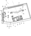
- 1 is a perspective view of an optical scanning device according to an embodiment of the present invention. It is a top view of the optical scanning device concerning one embodiment of the present invention. It is a bottom view of the optical scanning device concerning one embodiment of the present invention. It is a bottom view which shows the modification of the optical scanning device which concerns on one Embodiment of this invention.
- FIG. 1 is a schematic diagram showing an outline of a printer according to an embodiment of the present invention.
- the front side of the page in FIG. 1 is the front side (front side) of the printer 1, and the left and right directions are the printer. The direction when 1 is viewed from the front is used as a reference.
- the printer 1 includes a substantially rectangular parallelepiped housing 2 having a hollow portion. Below the inside of the housing 2, a cassette 3 containing paper is detachably mounted. A paper feed unit 4 that feeds paper from the paper feed cassette 3 is provided on the upper right side of the paper feed cassette 3.
- An image forming unit 5 is provided above the paper feeding unit 4.
- a photosensitive drum 6 is rotatably provided in the image forming unit 5, and a charging device 7, a developing device 8, a transfer roller 9, and a cleaning device 10 are disposed around the photosensitive drum 6. It arrange
- FIG. The developing device 8 is connected to the toner container 11.
- an optical scanning device 12 including a laser scanning unit (LSU) is provided on the left side of the image forming unit 5.
- a fixing device 14 is provided above the image forming unit 5, and a paper discharge unit 15 is provided on the left side of the fixing device 14.
- the paper discharge unit 15 faces a paper discharge tray 16 formed on the upper surface of the housing 2.
- paper is conveyed from the paper feeding unit 4 to the paper discharge unit 15 through the transfer nip 18 and the fixing device 14 formed between the photosensitive drum 6 and the transfer roller 9.
- a path 19 is provided.
- the sheet fed from the sheet feeding cassette 3 by the sheet feeding unit 4 is transported along the transport path 19 and transported to the transfer nip 18 in synchronization with the image forming operation described above.
- the toner image on the drum 6 is transferred to the paper.
- the sheet on which the toner image has been transferred is conveyed downstream in the conveyance path 19 and enters the fixing device 14 where the toner image is fixed on the sheet.
- the paper on which the toner image is fixed is discharged from the paper discharge unit 15 to the paper discharge tray 16.
- FIGS. 2 is a perspective view of the optical scanning device
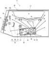
- FIG. 3 is a plan view of the optical scanning device
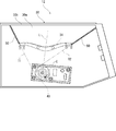
- FIG. 4 is a bottom view of the optical scanning device.
- the optical scanning device 12 includes an optical housing 30. Inside the optical housing 30 are a laser light source 31 that emits laser light, an optical component group 32 that shapes the emitted laser light, a deflector 33 that deflects the shaped laser light, and the deflected laser light. And an f ⁇ lens 34 as an optical element that forms an image on the photosensitive drum 6 are arranged along the path of the laser beam (see the two-dot chain line in FIG. 2). Further, the optical housing 30 houses a reflection mirror 35 for beam detection.
- the optical housing 30 is a pentagonal flat box-like member in plan view, and is formed by a bottom plate 30a and a side plate 30b erected from the outer periphery of the bottom plate 30a. A slit 37 is formed in one side plate 30b.
- the optical housing 30 is made of a resin having a low linear expansion coefficient.
- a laser light source 31 is supported on the other side plate 30 b of the optical housing 30 so as to emit laser light toward the inside of the optical housing 30.
- an optical component group 32 including a collimating lens 39, an aperture plate 40, and a cylindrical lens 41 is disposed in order along the traveling direction of the laser light.
- the laser light emitted from the laser light source 31 is converted into parallel light by the collimating lens 39, and then shaped into a desired beam shape by passing through the aperture plate 40, and is a line extending in the main scanning direction by the cylindrical lens 41.
- An image is formed and incident on the deflector 33.
- the deflector 33 includes a pentagonal polygon mirror 43 in plan view, a polygon motor 44 that is a driving source for rotating the polygon mirror 43, and a control board 45 on which the polygon motor 44 is supported.
- the control board 45 supports an electronic component such as an IC chip 46 for controlling the driving of the polygon motor 44 and a connector 47.
- the polygon mirror 43 is rotationally driven in the counterclockwise direction of FIGS. 2 and 3 by the polygon motor 44, so that the laser light that has passed through the cylindrical lens 41 is deflected in the scanning direction.
- the f ⁇ lens 34 has an entrance surface 34 a and an exit surface 34 b, and is disposed inside the side plate 30 b where the slit 37 is formed, along the scanning direction of the laser light deflected by the polygon mirror 43. Yes. Both ends of the f ⁇ lens 34 are supported on the bottom plate 30 a by the support member 48. The laser beam deflected by the polygon mirror 43 enters the incident surface 34 a, is emitted from the output surface 34 b, and forms an image on the photosensitive drum 6 through the slit 37.
- the beam detection reflecting mirror 35 is supported on the side of the f ⁇ lens 34 on the bottom plate 30 a of the optical housing 30. A part of the scanning light reflected by the polygon mirror 43 is incident on the beam detection reflecting mirror 35 and reflected toward the BD sensor (not shown). When the BD sensor detects the scanning light, it outputs a scanning start signal, and the laser light source 31 starts image writing.
- the bearings of the polygon motor 44 and the IC chip 46 generate heat, and the air around the control board 45 is heated.
- the heated air is diffused in the optical housing 30 along with the airflow generated with the rotation of the polygon mirror 43, and the air in the optical housing 30 becomes high temperature.
- this region has a lower temperature than the other regions. That is, the region R between the emission surface 34b of the f ⁇ lens 34 and the side plate 30b of the optical housing 30 between both ends of the f ⁇ lens 34 in the scanning direction of the laser light deflected by the deflector 33 is larger than the other regions. The temperature goes down.
- reinforcing ribs 50 are erected on the back surface of the bottom plate 30 a of the optical housing 30.
- the reinforcing rib 50 is formed on the back surface of the bottom plate 30a of the optical housing 30 so as to extend from both ends of the f ⁇ lens 34 in the scanning direction to the downstream side in the laser beam traveling direction. ing. More specifically, the reinforcing rib 50 reaches the side plate 30b from both ends of the f ⁇ lens 34 in the scanning direction on the tangent lines T1 and T2 along the rotation direction of the polygon mirror 43 from the outer circumferential circle C of the rotation locus of the polygon mirror 43. Is formed.
- the temperatures on the boundary between the high temperature portion and the low temperature portion indicated by these tangent lines T1 and T2 are expected to be substantially equal, and the reinforcing rib 50 is formed on this boundary (isothermal line).
- the reinforcing rib 50 is formed asymmetrically with respect to the line L connecting the rotation axis of the polygon mirror 43 and the center of the f ⁇ lens 34.
- the reinforcing rib 50 formed on the back surface of the optical housing 30 is almost equal to the isotherm at the boundary between the high temperature portion and the low temperature portion inside the optical housing 30. Therefore, the reinforcing rib 50 itself is isothermal. For this reason, when heated, the optical housing 30 can be uniformly deformed in all directions, and the optical housing 30 can be similarly deformed. Therefore, when the optical housing 30 is thermally deformed by heat generated by the polygon motor 44 or the control board 45, the relative positional relationship among the optical component group 32, the deflector 33, and the f ⁇ lens 34 does not change. The irradiation position of the laser beam to the lens does not change, and image defects can be suppressed.
- the reinforcing rib 50 is erected on the back surface of the bottom plate 30 a of the optical housing 30, it is possible to prevent interference between the optical component and the like accommodated in the optical housing 30 and the reinforcing rib 50.
- the reinforcing rib 50 may be formed on the upper surface of the bottom plate 30 a of the optical housing 30 when the arrangement of the optical component group 32 is not restricted.
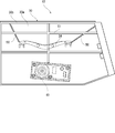
- FIG. 5 is a view showing a modification of the reinforcing rib 50.
- FIG. 5 is a rear view of the optical housing.
- lattice-like ribs 51 are provided on the back surface of the bottom plate 30 a of the optical housing 30 so as to be integrated with the reinforcing ribs 50 to give rigidity against vibration caused by rotation of the polygon mirror 43.
- the grid-like ribs 51 are continuously formed in the high-temperature part and the low-temperature part, the grid-like ribs 51 themselves have a temperature distribution and cause non-uniform deformation. There is a possibility that the deformation of the optical housing 30 may be promoted.
- the reinforcing ribs 50 for suppressing deformation of the optical housing 30 integrally with the grid-like ribs 51 by providing the reinforcing ribs 50 for suppressing deformation of the optical housing 30 integrally with the grid-like ribs 51, the thermal deformation of the grid-like ribs 51 can be reduced.
- the layout of the reinforcing ribs 50 and the grid ribs 51 for suppressing deformation in consideration of the balance between ensuring the rigidity of the optical housing 30 and suppressing thermal deformation.
- the grid-like ribs 51 may be formed independently in the high temperature part and the low temperature part (so as not to be continuous with the high temperature part and the low temperature part).
- the optical scanning device has a configuration in which the laser light emitted from the f ⁇ lens 34 travels straight toward the photosensitive drum 6, but has a configuration in which the photosensitive drum 6 is irradiated via a folding mirror. You can also Further, the present invention can also be applied to a counter scanning optical scanning device in which the pair of optical component groups 32 and the f ⁇ lens 34 are arranged symmetrically with respect to the deflector 33.
- the present invention is applied to an image forming apparatus other than the printer 1 such as a copying machine, a facsimile machine, and a multifunction machine. You may apply the structure of invention.
Landscapes
- Physics & Mathematics (AREA)
- General Physics & Mathematics (AREA)
- Optics & Photonics (AREA)
- Engineering & Computer Science (AREA)
- Multimedia (AREA)
- Signal Processing (AREA)
- Mechanical Optical Scanning Systems (AREA)
- Facsimile Scanning Arrangements (AREA)
- Laser Beam Printer (AREA)
Abstract
光走査装置(12)は、回転することで光源(31)から射出された光を所定の走査方向に偏向するポリゴンミラー(43)と、該ポリゴンミラー(43)で偏向された光を結像する光学素子(34)と、前記ポリゴンミラー(43)を回転させる駆動源(44)と、該駆動源(44)の駆動を制御する制御基板(45)と、前記ポリゴンミラー(43)と前記光学素子(34)と前記駆動源(44)と前記制御基板(45)とが収容される光学ハウジング(30)と、を備える。前記光学ハウジング(30)は、前記走査方向における前記光学素子(34)の両端部から前記ポリゴンミラー(43)で偏向された前記光の進行方向下流側に向かうように立設される補強リブ(50)を有している。
Description
本発明は、感光体ドラムにレーザー光を走査して露光する光走査装置及びこの光走査装置を備えた画像形成装置に関する。
プリンターや複写機等の画像形成装置では、レーザー・スキャンニング・ユニット(LSU)で構成される光走査装置から感光体ドラムにレーザー光を露光して静電潜像を形成し、この静電潜像をトナーで現像することで画像が形成されている。
近年では画像形成装置の高画質化や高速化が進んでおり、光走査装置においても、レーザー光を偏向するポリゴンミラーの回転速度の高速化が要求されている。ただし、ポリゴンミラーの回転速度を高速化すると、ポリゴンミラーを回転させるポリゴンモーターやポリゴンモーターの駆動を制御する制御基板からの発熱量が増える。その結果、光走査装置の光学ハウジングが熱変形し、光学ハウジングに支持される光学部品の位置や姿勢が変動して、レーザー光が適切な位置に走査されず、画像不良が生じるという問題が生じる。
ポリゴンモーターや制御基板の発熱による光学ハウジングの変形を改善するために、特許文献1~特許文献8に記載されているように、様々な対策が提案されている。特許文献1に記載されている光走査装置では、光学ハウジングを画像形成装置の装置本体に対して、回動可能且つスライド可能に支持させて、光学ハウジングを自由膨張させることで光学部品の相対位置の変化を低減させている。特許文献2に記載されている光走査装置では、光学ハウジングを、比較的剛性の低い部分で画像形成装置の装置本体に固定することで、光学ハウジングの各部の熱変形を均一化させている。
また、特許文献3に記載されている光走査装置では、光学ハウジング内に流路を形成し、この流路内に制御基板が配置され、流路外に他の光学部品を配置することで、制御基板によって加熱された空気を循環させて、光学ハウジングの温度勾配と少なくさせている。特許文献4に記載されている光走査装置では、光学ハウジングの底板に制御基板の裏面を露出させる切り欠き穴を形成することで、制御基板の冷却を図っている。
さらに、特許文献5に記載されている光走査装置では、ポリゴンモーターの近傍に上下に貫通するダクトを形成し、ダクトに冷却風を送ることで光学ハウジングの温度上昇を抑えている。特許文献6に記載されている光走査装置では、ポリゴンモーターと、発熱源である光源ユニットとを、光学ハウジング内に対称に配置することで、光学ハウジング内の温度を均一化させている。
特許文献7に記載されている光走査装置は、制御基板をポリゴンモーターと分離させて、光学ハウジングの側板の外面に配置することで、光学ハウジングの底板の温度上昇を防ぐように構成されている。また、特許文献8は、光学素子群がポリゴンミラーに対して対称に配置された光走査装置において、ポリゴンモーターを中心として対称として、底板の上面と下面とにリブを形成し、リブの膨張による光軸のずれ方向が感光体ドラム上で同じ方向となるように構成されている。
このように、ポリゴンモーターや制御基板からの発熱量を減少させる方法(特許文献4、特許文献5、特許文献7)や、光学ハウジングを相似的に変形可能に構成する方法(特許文献1、特許文献8)、光学ハウジング内の温度分布を一定にする方法(特許文献2、特許文献3、特許文献6)等が提案されている。
ところで、画像形成装置では、高画質化及び高速化と共に省スペース化も進んでいる。画像形成装置の省スペース化に対応して光走査装置を小型化するために、光学ハウジング内に支持される光学部品は、互いの間隔を短くして密接に配置されている。
光学ハウジングにおいては、ポリゴンモーターと制御基板からの発熱で光学ハウジング自体が加熱されるだけではなく、ポリゴンモーターと制御基板の近傍で加熱された高温の空気が、高速回転するポリゴンミラーから発生する気流に沿って光学ハウジング内に拡散されることで内部の温度が上昇する。ただし、前述のように、光学ハウジング内には光学部品が密接に配置されているので、気流がこれらの光学部品で遮られることで内部の温度分布は不均一となる。つまり、気流が行き渡る場所では高温になり、気流が行き渡らない場所では低温になる。このような不均一な温度分布によって、光学ハウジングが不均一に変形し、光学部品の姿勢や位置が変動してしまう問題が生じる。
しかしながら、上記の特許文献に記載された光走査装置では、このような光学ハウジング内の不均一な気流に起因する熱変形は考慮されていない。特許文献3には、ポリゴンミラーの回転によって生じる気流を循環させるための流路が光学ハウジングに形成されているが、このような流路を形成する場合には、光学部品を避けて形成する必要があるために、流路の形状が複雑になって、気流がスムーズに流れなくなったり、光学ハウジングが大型化したりするという問題がある。また、ポリゴンミラーによるレーザー光の走査方向の範囲には流路を形成することができないので、この範囲内では特に温度が上昇してしまう虞がある。
本発明は上記事情を考慮し、光学ハウジングの内部の温度分布が不均一な場合でも、光学ハウジングを相似的に変形させることで発熱の影響を低減した光走査装置及び画像形成装置を提供することを目的とする。
本発明の光走査装置は、回転することで光源から射出された光を所定の走査方向に偏向するポリゴンミラーと、該ポリゴンミラーで偏向された光を結像する光学素子と、前記ポリゴンミラーを回転させる駆動源と、該駆動源の駆動を制御する制御基板と、前記ポリゴンミラーと前記光学素子と前記駆動源と前記制御基板とが収容される光学ハウジングと、を備え、前記光学ハウジングは、前記走査方向における前記光学素子の両端部から前記ポリゴンミラーで偏向された前記光の進行方向下流側に向かうように立設される補強リブを有していることを特徴とする。
本発明の画像形成装置は、前記に記載の光走査装置を備えていることを特徴とする。
本発明によれば、ポリゴンミラーの回転によって発生する気流が遮られることで生じる低温部と高温部との境界のほぼ温度の等しい部分に補強リブが形成されるので、補強リブ自体は等温となり、加熱された際には全方向に均等に変形し、光学ハウジングを相似的に変形させることができる。したがって、光学ハウジングの不均一な熱変形による画像不良を防止できる。
以下、図面を参照しつつ、本発明の一実施形態に係る光走査装置及び画像形成装置について説明する。
まず、図1を参照して、画像形成装置としてのプリンター1の全体の構成について説明する。図1は、本発明の一実施形態に係るプリンターの概略を示す模式図であり、以下の説明では、図1における紙面手前側を、プリンター1の正面側(前側)とし、左右の向きはプリンター1を正面から見た方向を基準とする。
プリンター1は、中空部を有する略直方体形状の筐体2を備えている。筐体2の内部の下方には、用紙を収納したカセット3が着脱自在に装着されている。給紙カセット3の右上方には、給紙カセット3から用紙を給紙する給紙部4が設けられている。
給紙部4の上方には、画像形成部5が設けられている。画像形成部5には、感光体ドラム6が回転可能に設けられ、感光体ドラム6の周囲には、帯電装置7と、現像装置8と、転写ローラー9と、クリーニング装置10とが、感光体ドラム6の回転方向(図1の矢印X参照)に沿って配置されている。現像装置8は、トナーコンテナ11と接続している。画像形成部5の左方には、レーザー・スキャニング・ユニット(LSU)で構成される光走査装置12が備えられている。
画像形成部5の上方には、定着装置14が備えられており、定着装置14の左方には排紙部15が設けられている。排紙部15は筐体2の上面に形成された排紙トレイ16に面している。
また、筐体2の内部には、給紙部4から、感光体ドラム6と転写ローラー9との間に形成される転写ニップ18と定着装置14を通って排紙部15へ向かう用紙の搬送経路19が設けられている。
次に、このような構成を備えたプリンター1の画像形成動作について説明する。帯電装置7によって感光体ドラム6の表面が帯電された後、光走査装置12からのレーザー光(矢印P参照)により感光体ドラム6に対して画像データに対応した露光が行われ、感光体ドラム6の表面に静電潜像が形成される。静電潜像は現像装置8によりトナー像に現像される。感光体ドラム6上に残留したトナーはクリーニング装置10によって除去される。
一方、給紙カセット3から給紙部4によって送り出された用紙は搬送経路19に沿って搬送され、上記した画像形成動作とタイミングを合わせて転写ニップ18へ搬送され、転写ニップ18において、感光体ドラム6上のトナー像が用紙に転写される。トナー像を転写された用紙は、搬送経路19を下流側へと搬送されて定着装置14に進入し、定着装置14において用紙にトナー像が定着される。トナー像が定着された用紙は、排紙部15から排紙トレイ16に排出される。
次に、図2~図4を参照して、光走査装置12について説明する。図2は光走査装置の斜視図、図3は光走査装置の平面図、図4は光走査装置の底面図である。
光走査装置12は、光学ハウジング30を備える。光学ハウジング30の内部には、レーザー光を出射するレーザー光源31と、出射されたレーザー光を整形する光学部品群32と、整形されたレーザー光を偏向する偏向器33と、偏向されたレーザー光を感光体ドラム6上に結像する光学素子としてのfθレンズ34と、がレーザー光の進路(図2の二点鎖線参照)に沿って配置されている。さらに、光学ハウジング30には、ビーム検出用反射ミラー35が収容されている。
光学ハウジング30は、平面視にて五角形状の扁平な箱状の部材であり、底板30aと、底板30aの外周縁から立設された側板30bと、によって形成されている。一つの側板30bには、スリット37が形成されている。光学ハウジング30は、線膨張係数の低い樹脂等で形成されている。
光学ハウジング30の他の側板30bには、光学ハウジング30の内部に向かってレーザー光を出射するように、レーザー光源31が支持されている。光学ハウジング30の底板30a上には、レーザー光の進行方向に沿って順に、コリメートレンズ39と、アパーチャー板40と、シリンドリカルレンズ41、を有する光学部品群32が配置されている。レーザー光源31から出射されたレーザー光は、コリメートレンズ39によって平行光に変換された後、アパーチャー板40を通過することで所望のビーム形状に成形され、シリンドリカルレンズ41によって、主走査方向に延びる線像に結像されて偏向器33に入射する。
偏向器33は、平面視にて五角形状のポリゴンミラー43と、ポリゴンミラー43を回転させる駆動源であるポリゴンモーター44と、ポリゴンモーター44が支持される制御基板45と、を有する。制御基板45には、ポリゴンモーター44の駆動を制御するICチップ46等の電子部品やコネクタ47が支持されている。ポリゴンミラー43がポリゴンモーター44によって図2、図3の反時計回り方向に回転駆動されることで、シリンドリカルレンズ41を通過したレーザー光が、走査方向に偏向される。
fθレンズ34は、入射面34aと出射面34bとを有しており、スリット37が形成された側板30bの内側に、ポリゴンミラー43で偏向されたレーザー光の走査方向に沿うように配置されている。fθレンズ34の両端は支持部材48によって底板30aに支持されている。ポリゴンミラー43で偏向されたレーザー光は入射面34aに入射し、出射面34bから出射されて、スリット37を通して感光体ドラム6上に結像する。
ビーム検出用反射ミラー35は、光学ハウジング30の底板30a上の、fθレンズ34の側方に支持されている。ビーム検出用反射ミラー35には、ポリゴンミラー43で反射した走査光の一部が入射し、BDセンサー(図示省略)に向かって反射する。BDセンサーは走査光を検知すると、走査開始信号を出力して、レーザー光源31が画像書き込みを開始する。
次に、上記の光走査装置12における光学ハウジング30内の温度分布について、図3を参照して説明する。ポリゴンミラー43が高速で回転すると、ポリゴンミラー43を中心にして回転方向(図3の反時計回り方向)に沿うように気流(図3の矢印参照)が発生する。この気流は、ポリゴンミラー43の周辺から光学ハウジング30の側板30bの方向に拡散する。しかし、fθレンズ34の方向に向かう気流はfθレンズ34で遮られるので、fθレンズ34の出射面34bの側の領域には気流が達しない。
また、ポリゴンミラー43が高速で回転すると、ポリゴンモーター44の軸受やICチップ46が発熱し、制御基板45の周囲の空気が加熱される。加熱された空気は、ポリゴンミラー43の回転に伴って発生する気流に乗って光学ハウジング30内に拡散され、光学ハウジング30内の空気が高温になる。しかし、前述のように、fθレンズ34の出射面34b側の領域には気流が達しないので、この領域は他の領域よりも低温となる。つまり、偏向器33で偏向されたレーザー光の走査方向におけるfθレンズ34の両端間の、fθレンズ34の出射面34bと光学ハウジング30の側板30bとの間の領域Rは、他の領域よりも温度が低くなる。
このような光学ハウジング30の温度分布を考慮して、図4に示されるように、光学ハウジング30の底板30aの裏面には、補強リブ50が立設されている。
本実施形態の光走査装置12においては、補強リブ50は、光学ハウジング30の底板30aの裏面に、走査方向におけるfθレンズ34の両端から、レーザー光の進行方向の下流側に延びるように形成されている。詳細には、補強リブ50は、ポリゴンミラー43の回転軌跡の外周円Cからポリゴンミラー43の回転方向に沿った接線T1、T2上において、走査方向におけるfθレンズ34の両端から側板30bに達するように形成されている。つまり、これらの接線T1、T2で示される高温部と低温部との境界上の温度はほぼ等しいと予想され、この境界(等温線)上に補強リブ50が形成されることになる。なお、このようにポリゴンミラー43の回転によって生じる気流に沿わせることで、補強リブ50はポリゴンミラー43の回転軸とfθレンズ34の中心とを結ぶ線Lに対しては非対称に形成される。
上記説明したように本発明の光走査装置12によれば、光学ハウジング30の裏面に形成された補強リブ50は、光学ハウジング30の内部における高温部と低温部との境界の等温線にほぼ一致しているので、補強リブ50自体は等温となる。このため、加熱された際には全方向に均等に変形し、光学ハウジング30を相似的に変形させることができる。したがって、ポリゴンモーター44や制御基板45の発熱によって光学ハウジング30が熱変形する際に、光学部品群32や偏向器33、fθレンズ34の相対的な位置関係は変化しないので、感光体ドラム6上へのレーザー光の照射位置は変化せず、画像不良を抑制できる。
また、補強リブ50を光学ハウジング30の底板30aの裏面に立設したので、光学ハウジング30内に収容される光学部品等と補強リブ50との干渉を防止できる。なお、光学部品群32の配置の制約を受けない場合は、補強リブ50は光学ハウジング30の底板30aの上面に形成してもよい。
図5は、補強リブ50の変形例を示す図である。図5は光学ハウジングの裏面図である。この変形例では、光学ハウジング30の底板30aの裏面に、ポリゴンミラー43の回転による振動に対する剛性を与えるための格子状のリブ51が補強リブ50と一体に立設されている。図3に示される温度分布を考慮すると、格子状リブ51は高温部と低温部とに連続して形成されているので、格子状リブ51自体が温度分布を持ち、不均一な変形を起こして光学ハウジング30の変形を助長してしまう虞がある。
そこで、本実施形態のように、光学ハウジング30の変形抑制用の補強リブ50を格子状リブ51に一体に設けることで、格子状リブ51の熱変形を低減することができる。ただし、このような格子状リブ51を設けずに、変形抑制用の補強リブ50のみを設けた場合の方が、光学ハウジング30の熱変形の抑制には効果がある。このため、光学ハウジング30の剛性確保と熱変形抑制とのバランスを考慮して変形抑制用の補強リブ50と格子状リブ51のレイアウトを設定することが好ましい。例えば、格子状リブ51を高温部と低温部とにそれぞれ独立して(高温部と低温部とに連続しないように)形成してもよい。
なお、本実施形態の光走査装置は、fθレンズ34から出射されたレーザー光が感光体ドラム6に向かって直進する構成を有するが、折り返しミラーを介して感光体ドラム6に照射される構成とすることもできる。また、一対の光学部品群32及びfθレンズ34が偏向器33に対して対称に配置された対向走査方式の光走査装置にも適用することができる。
さらに、本発明の実施形態では、プリンター1に本発明の構成を適用した場合について説明したが、他の異なる実施形態では、複写機、ファクシミリ、複合機等のプリンター1以外の画像形成装置に本発明の構成を適用しても良い。
さらに、上記した本発明の実施形態の説明は、本発明に係る光走査装置及び画像形成装置における好適な実施の形態を説明しているため、技術的に好ましい種々の限定を付している場合もあるが、本発明の技術範囲は、特に本発明を限定する記載がない限り、これらの態様に限定されるものではない。すなわち、上記した本発明の実施の形態における構成要素は適宜、既存の構成要素等との置き換えが可能であり、かつ、他の既存の構成要素との組合せを含む様々なバリエーションが可能であり、上記した本発明の実施の形態の記載をもって、特許請求の範囲に記載された発明の内容を限定するものではない。
Claims (7)
- 回転することで光源から射出された光を所定の走査方向に偏向するポリゴンミラーと、
該ポリゴンミラーで偏向された光を結像する光学素子と、
前記ポリゴンミラーを回転させる駆動源と、
該駆動源の駆動を制御する制御基板と、
前記ポリゴンミラーと前記光学素子と前記駆動源と前記制御基板とが収容される光学ハウジングと、を備え、
前記光学ハウジングは、前記走査方向における前記光学素子の両端部から前記ポリゴンミラーで偏向された前記光の進行方向下流側に向かうように立設される補強リブを有していることを特徴とする光走査装置。 - 前記光学ハウジングは、
前記ポリゴンミラーと前記光学素子と前記駆動源と前記制御部とが支持される底板と、
該底板の外周縁から立設された側板と、を有し、
前記補強リブは、前記ポリゴンミラーの回転軌跡の外周円から前記ポリゴンミラーの回転方向下流側に向かう接線上において、前記走査方向における前記光学素子の両端部から前記側板に向かうように前記底板に立設されていることを特徴とする請求項1に記載の光走査装置。 - 前記補強リブは、前記ポリゴンミラーの回転によって発生する気流の拡散方向における前記光学素子の両端部から、前記拡散方向下流側に向かうように立設されることを特徴とする請求項1に記載の光走査装置。
- 前記補強リブは、前記光学ハウジングの前記底板の裏面に形成されていることを特徴とする請求項2に記載の光走査装置。
- 前記光学ハウジングは、剛性付与用のリブを有し、前記補強リブは前記剛性付与用リブと一体に形成されていることを特徴とする請求項1に記載の光走査装置。
- 前記光学素子はfθレンズであることを特徴とする請求項1に記載の光走査装置。
- 請求項1に記載の光走査装置を備えていることを特徴とする画像形成装置。
Priority Applications (1)
| Application Number | Priority Date | Filing Date | Title |
|---|---|---|---|
| JP2017525167A JP6493528B2 (ja) | 2015-06-23 | 2016-06-08 | 光走査装置及び画像形成装置 |
Applications Claiming Priority (2)
| Application Number | Priority Date | Filing Date | Title |
|---|---|---|---|
| JP2015125728 | 2015-06-23 | ||
| JP2015-125728 | 2015-06-23 |
Publications (1)
| Publication Number | Publication Date |
|---|---|
| WO2016208395A1 true WO2016208395A1 (ja) | 2016-12-29 |
Family
ID=57585071
Family Applications (1)
| Application Number | Title | Priority Date | Filing Date |
|---|---|---|---|
| PCT/JP2016/067079 Ceased WO2016208395A1 (ja) | 2015-06-23 | 2016-06-08 | 光走査装置及び画像形成装置 |
Country Status (2)
| Country | Link |
|---|---|
| JP (1) | JP6493528B2 (ja) |
| WO (1) | WO2016208395A1 (ja) |
Citations (3)
| Publication number | Priority date | Publication date | Assignee | Title |
|---|---|---|---|---|
| JP2005122021A (ja) * | 2003-10-20 | 2005-05-12 | Ricoh Co Ltd | 光学ビーム走査装置およびそれを備えた画像形成装置 |
| JP2010224269A (ja) * | 2009-03-24 | 2010-10-07 | Kyocera Mita Corp | 光走査装置及び画像形成装置 |
| JP2011186420A (ja) * | 2010-02-15 | 2011-09-22 | Ricoh Co Ltd | 光走査装置および画像形成装置 |
-
2016
- 2016-06-08 JP JP2017525167A patent/JP6493528B2/ja not_active Expired - Fee Related
- 2016-06-08 WO PCT/JP2016/067079 patent/WO2016208395A1/ja not_active Ceased
Patent Citations (3)
| Publication number | Priority date | Publication date | Assignee | Title |
|---|---|---|---|---|
| JP2005122021A (ja) * | 2003-10-20 | 2005-05-12 | Ricoh Co Ltd | 光学ビーム走査装置およびそれを備えた画像形成装置 |
| JP2010224269A (ja) * | 2009-03-24 | 2010-10-07 | Kyocera Mita Corp | 光走査装置及び画像形成装置 |
| JP2011186420A (ja) * | 2010-02-15 | 2011-09-22 | Ricoh Co Ltd | 光走査装置および画像形成装置 |
Also Published As
| Publication number | Publication date |
|---|---|
| JPWO2016208395A1 (ja) | 2018-02-22 |
| JP6493528B2 (ja) | 2019-04-03 |
Similar Documents
| Publication | Publication Date | Title |
|---|---|---|
| US20150029284A1 (en) | Light scanning apparatus | |
| JP2009251308A (ja) | 光学走査装置及びカラー画像形成装置 | |
| JP6349896B2 (ja) | 画像形成装置 | |
| JP6493528B2 (ja) | 光走査装置及び画像形成装置 | |
| JP2010128359A (ja) | 光走査装置、この光走査装置を備えた画像形成装置 | |
| JP4884035B2 (ja) | 光書き込み装置 | |
| JP5061178B2 (ja) | 光走査装置及び画像形成装置 | |
| US20170227882A1 (en) | Light scanning device that ensures improved flexible location of component for regulating expanded widths of light beam | |
| JP2023087631A (ja) | 光走査装置および画像形成装置 | |
| US9304471B2 (en) | Image forming apparatus, discharge tray used in image forming apparatus | |
| JP5589108B2 (ja) | 光走査装置及び画像形成装置 | |
| JP5255795B2 (ja) | 画像形成装置 | |
| JP5238732B2 (ja) | 光走査装置及び画像形成装置 | |
| US12372894B2 (en) | Optical scanning apparatus and image forming apparatus | |
| JP2015200852A (ja) | 光走査装置及び該光走査装置を備えた画像形成装置 | |
| JP6269070B2 (ja) | 定着装置および画像形成装置 | |
| JP2010049042A (ja) | 画像形成装置 | |
| JP5219950B2 (ja) | 光走査装置 | |
| JP5996142B1 (ja) | 画像形成装置 | |
| JP2010224268A (ja) | 光走査装置及び画像形成装置 | |
| JP5151899B2 (ja) | 走査装置および画像形成装置 | |
| JP2006003503A (ja) | 画像形成装置 | |
| JP5297597B2 (ja) | 走査光学装置及びこれを搭載した画像形成装置 | |
| JP2010217240A (ja) | 光源装置、光走査装置およびそれを備えた画像形成装置 | |
| JP2001242672A (ja) | 画像形成装置 |
Legal Events
| Date | Code | Title | Description |
|---|---|---|---|
| 121 | Ep: the epo has been informed by wipo that ep was designated in this application |
Ref document number: 16814166 Country of ref document: EP Kind code of ref document: A1 |
|
| ENP | Entry into the national phase |
Ref document number: 2017525167 Country of ref document: JP Kind code of ref document: A |
|
| NENP | Non-entry into the national phase |
Ref country code: DE |
|
| 122 | Ep: pct application non-entry in european phase |
Ref document number: 16814166 Country of ref document: EP Kind code of ref document: A1 |