WO2016204122A1 - 半導体装置 - Google Patents
半導体装置 Download PDFInfo
- Publication number
- WO2016204122A1 WO2016204122A1 PCT/JP2016/067584 JP2016067584W WO2016204122A1 WO 2016204122 A1 WO2016204122 A1 WO 2016204122A1 JP 2016067584 W JP2016067584 W JP 2016067584W WO 2016204122 A1 WO2016204122 A1 WO 2016204122A1
- Authority
- WO
- WIPO (PCT)
- Prior art keywords
- circuit
- signal
- overcurrent detection
- output
- potential
- Prior art date
- Legal status (The legal status is an assumption and is not a legal conclusion. Google has not performed a legal analysis and makes no representation as to the accuracy of the status listed.)
- Ceased
Links
Images



Classifications
-
- H—ELECTRICITY
- H02—GENERATION; CONVERSION OR DISTRIBUTION OF ELECTRIC POWER
- H02M—APPARATUS FOR CONVERSION BETWEEN AC AND AC, BETWEEN AC AND DC, OR BETWEEN DC AND DC, AND FOR USE WITH MAINS OR SIMILAR POWER SUPPLY SYSTEMS; CONVERSION OF DC OR AC INPUT POWER INTO SURGE OUTPUT POWER; CONTROL OR REGULATION THEREOF
- H02M1/00—Details of apparatus for conversion
- H02M1/08—Circuits specially adapted for the generation of control voltages for semiconductor devices incorporated in static converters
- H02M1/084—Circuits specially adapted for the generation of control voltages for semiconductor devices incorporated in static converters using a control circuit common to several phases of a multi-phase system
-
- G—PHYSICS
- G11—INFORMATION STORAGE
- G11C—STATIC STORES
- G11C11/00—Digital stores characterised by the use of particular electric or magnetic storage elements; Storage elements therefor
- G11C11/21—Digital stores characterised by the use of particular electric or magnetic storage elements; Storage elements therefor using electric elements
- G11C11/34—Digital stores characterised by the use of particular electric or magnetic storage elements; Storage elements therefor using electric elements using semiconductor devices
- G11C11/40—Digital stores characterised by the use of particular electric or magnetic storage elements; Storage elements therefor using electric elements using semiconductor devices using transistors
- G11C11/401—Digital stores characterised by the use of particular electric or magnetic storage elements; Storage elements therefor using electric elements using semiconductor devices using transistors forming cells needing refreshing or charge regeneration, i.e. dynamic cells
- G11C11/4063—Auxiliary circuits, e.g. for addressing, decoding, driving, writing, sensing or timing
- G11C11/407—Auxiliary circuits, e.g. for addressing, decoding, driving, writing, sensing or timing for memory cells of the field-effect type
- G11C11/409—Read-write [R-W] circuits
- G11C11/4091—Sense or sense/refresh amplifiers, or associated sense circuitry, e.g. for coupled bit-line precharging, equalising or isolating
-
- H—ELECTRICITY
- H02—GENERATION; CONVERSION OR DISTRIBUTION OF ELECTRIC POWER
- H02M—APPARATUS FOR CONVERSION BETWEEN AC AND AC, BETWEEN AC AND DC, OR BETWEEN DC AND DC, AND FOR USE WITH MAINS OR SIMILAR POWER SUPPLY SYSTEMS; CONVERSION OF DC OR AC INPUT POWER INTO SURGE OUTPUT POWER; CONTROL OR REGULATION THEREOF
- H02M1/00—Details of apparatus for conversion
- H02M1/32—Means for protecting converters other than automatic disconnection
-
- H—ELECTRICITY
- H02—GENERATION; CONVERSION OR DISTRIBUTION OF ELECTRIC POWER
- H02M—APPARATUS FOR CONVERSION BETWEEN AC AND AC, BETWEEN AC AND DC, OR BETWEEN DC AND DC, AND FOR USE WITH MAINS OR SIMILAR POWER SUPPLY SYSTEMS; CONVERSION OF DC OR AC INPUT POWER INTO SURGE OUTPUT POWER; CONTROL OR REGULATION THEREOF
- H02M7/00—Conversion of AC power input into DC power output; Conversion of DC power input into AC power output
- H02M7/42—Conversion of DC power input into AC power output without possibility of reversal
- H02M7/44—Conversion of DC power input into AC power output without possibility of reversal by static converters
- H02M7/48—Conversion of DC power input into AC power output without possibility of reversal by static converters using discharge tubes with control electrode or semiconductor devices with control electrode
-
- H—ELECTRICITY
- H03—ELECTRONIC CIRCUITRY
- H03K—PULSE TECHNIQUE
- H03K17/00—Electronic switching or gating, i.e. not by contact-making and –breaking
- H03K17/08—Modifications for protecting switching circuit against overcurrent or overvoltage
- H03K17/081—Modifications for protecting switching circuit against overcurrent or overvoltage without feedback from the output circuit to the control circuit
- H03K17/0812—Modifications for protecting switching circuit against overcurrent or overvoltage without feedback from the output circuit to the control circuit by measures taken in the control circuit
- H03K17/08122—Modifications for protecting switching circuit against overcurrent or overvoltage without feedback from the output circuit to the control circuit by measures taken in the control circuit in field-effect transistor switches
-
- H—ELECTRICITY
- H03—ELECTRONIC CIRCUITRY
- H03K—PULSE TECHNIQUE
- H03K17/00—Electronic switching or gating, i.e. not by contact-making and –breaking
- H03K17/08—Modifications for protecting switching circuit against overcurrent or overvoltage
- H03K17/082—Modifications for protecting switching circuit against overcurrent or overvoltage by feedback from the output to the control circuit
- H03K17/0822—Modifications for protecting switching circuit against overcurrent or overvoltage by feedback from the output to the control circuit in field-effect transistor switches
-
- H—ELECTRICITY
- H03—ELECTRONIC CIRCUITRY
- H03K—PULSE TECHNIQUE
- H03K17/00—Electronic switching or gating, i.e. not by contact-making and –breaking
- H03K17/51—Electronic switching or gating, i.e. not by contact-making and –breaking characterised by the components used
- H03K17/56—Electronic switching or gating, i.e. not by contact-making and –breaking characterised by the components used by the use, as active elements, of semiconductor devices
- H03K17/687—Electronic switching or gating, i.e. not by contact-making and –breaking characterised by the components used by the use, as active elements, of semiconductor devices the devices being field-effect transistors
-
- H—ELECTRICITY
- H10—SEMICONDUCTOR DEVICES; ELECTRIC SOLID-STATE DEVICES NOT OTHERWISE PROVIDED FOR
- H10D—INORGANIC ELECTRIC SEMICONDUCTOR DEVICES
- H10D30/00—Field-effect transistors [FET]
-
- H—ELECTRICITY
- H10—SEMICONDUCTOR DEVICES; ELECTRIC SOLID-STATE DEVICES NOT OTHERWISE PROVIDED FOR
- H10D—INORGANIC ELECTRIC SEMICONDUCTOR DEVICES
- H10D30/00—Field-effect transistors [FET]
- H10D30/60—Insulated-gate field-effect transistors [IGFET]
- H10D30/64—Double-diffused metal-oxide semiconductor [DMOS] FETs
- H10D30/66—Vertical DMOS [VDMOS] FETs
-
- H—ELECTRICITY
- H10—SEMICONDUCTOR DEVICES; ELECTRIC SOLID-STATE DEVICES NOT OTHERWISE PROVIDED FOR
- H10D—INORGANIC ELECTRIC SEMICONDUCTOR DEVICES
- H10D62/00—Semiconductor bodies, or regions thereof, of devices having potential barriers
- H10D62/10—Shapes, relative sizes or dispositions of the regions of the semiconductor bodies; Shapes of the semiconductor bodies
-
- G—PHYSICS
- G11—INFORMATION STORAGE
- G11C—STATIC STORES
- G11C2211/00—Indexing scheme relating to digital stores characterized by the use of particular electric or magnetic storage elements; Storage elements therefor
- G11C2211/401—Indexing scheme relating to cells needing refreshing or charge regeneration, i.e. dynamic cells
- G11C2211/4013—Memory devices with multiple cells per bit, e.g. twin-cells
-
- H—ELECTRICITY
- H02—GENERATION; CONVERSION OR DISTRIBUTION OF ELECTRIC POWER
- H02M—APPARATUS FOR CONVERSION BETWEEN AC AND AC, BETWEEN AC AND DC, OR BETWEEN DC AND DC, AND FOR USE WITH MAINS OR SIMILAR POWER SUPPLY SYSTEMS; CONVERSION OF DC OR AC INPUT POWER INTO SURGE OUTPUT POWER; CONTROL OR REGULATION THEREOF
- H02M7/00—Conversion of AC power input into DC power output; Conversion of DC power input into AC power output
- H02M7/42—Conversion of DC power input into AC power output without possibility of reversal
- H02M7/44—Conversion of DC power input into AC power output without possibility of reversal by static converters
- H02M7/48—Conversion of DC power input into AC power output without possibility of reversal by static converters using discharge tubes with control electrode or semiconductor devices with control electrode
- H02M7/53—Conversion of DC power input into AC power output without possibility of reversal by static converters using discharge tubes with control electrode or semiconductor devices with control electrode using devices of a triode or transistor type requiring continuous application of a control signal
- H02M7/537—Conversion of DC power input into AC power output without possibility of reversal by static converters using discharge tubes with control electrode or semiconductor devices with control electrode using devices of a triode or transistor type requiring continuous application of a control signal using semiconductor devices only, e.g. single switched pulse inverters
- H02M7/5387—Conversion of DC power input into AC power output without possibility of reversal by static converters using discharge tubes with control electrode or semiconductor devices with control electrode using devices of a triode or transistor type requiring continuous application of a control signal using semiconductor devices only, e.g. single switched pulse inverters in a bridge configuration
-
- H—ELECTRICITY
- H03—ELECTRONIC CIRCUITRY
- H03K—PULSE TECHNIQUE
- H03K2217/00—Indexing scheme related to electronic switching or gating, i.e. not by contact-making or -breaking covered by H03K17/00
- H03K2217/0063—High side switches, i.e. the higher potential [DC] or life wire [AC] being directly connected to the switch and not via the load
-
- H—ELECTRICITY
- H03—ELECTRONIC CIRCUITRY
- H03K—PULSE TECHNIQUE
- H03K2217/00—Indexing scheme related to electronic switching or gating, i.e. not by contact-making or -breaking covered by H03K17/00
- H03K2217/0072—Low side switches, i.e. the lower potential [DC] or neutral wire [AC] being directly connected to the switch and not via the load
Definitions
- the present invention relates to a semiconductor device having an overcurrent protection function for detecting that an overcurrent has flowed through two power devices connected in a totem pole connection.
- the inverter or converter a circuit configuration is adopted in which the power devices are connected by totem pole connection, and the high-side and low-side power devices are driven by drive circuits, respectively. That is, on the high side, the signal generated with reference to the ground potential by the pulse generation circuit is level-shifted by the level shift circuit and then transmitted to the high-side drive circuit, thereby driving the high-side power device on / off. On the other hand, on the low side, a signal generated with reference to the ground potential is transmitted to the low side drive circuit, and the low side power device is driven on and off.
- the midpoint of the totem pole which is the connection point between the low-side power device and the high-side power device, is connected to an inductive load such as a motor. Therefore, external noise due to inductive load, parasitic inductance, etc. may be superimposed on the midpoint of the totem pole. In such a case, the midpoint potential of the totem pole becomes an overshoot or undershoot state depending on the magnitude of noise, timing, and the like. In other words, the midpoint potential of the totem pole becomes a potential higher than the high voltage potential of the high-side power device or a potential lower than the ground potential.
- an off signal may be output from the pulse generation circuit to the high-side power device.
- the level shift circuit cannot normally transmit the signal to the high side drive circuit. Then, the high-side power device cannot be turned off at the timing to be turned off and remains on, and the original switching function cannot be maintained.
- Patent Document 1 there is known a technique (for example, see Patent Document 1) that copes with being unable to be turned off at the timing to be turned off.
- the second off signal is output after a predetermined time has elapsed since the first off signal was output.
- the second off signal can be normally transmitted to the level shift circuit, thereby avoiding a functional malfunction. Yes.
- the level shift circuit determines that the reset signal for turning off the high-side power device is not normally transmitted and regenerates the second reset signal (for example, Patent Documents). 2).
- a semiconductor device described in Patent Document 2 includes a high-side potential detection circuit that detects a high-side potential, and a high-side potential determination circuit that outputs an event signal based on a change in the high-side potential detected by the high-side potential detection circuit. I have.
- the pulse generation circuit regenerates the reset signal in accordance with the event signal output from the high side potential determination circuit and the logical input signal input from the outside.
- the high-side potential determination circuit monitors the high-side potential (reference potential or power supply potential) detected by the high-side potential detection circuit, and the fluctuation of the high-side potential inhibits the transmission of the reset signal in the level shift circuit. If it is determined that there is, an event signal is output.
- the pulse generation circuit regenerates the reset signal when the timing at which the event signal is received from the high-side potential determination circuit overlaps with the generation timing of the reset signal. As described above, when the transmission of the reset signal is hindered by the external noise, the reset signal is regenerated, so that the high-side power device is reliably turned off.
- the present invention has been made in view of these points, and operates as a system even if a signal for turning off the high-side power device is delayed from the normal timing, causing a short circuit between the upper and lower arms.
- An object is to provide a semiconductor device capable of continuing the above.
- a high-side drive circuit that drives a high-side power device having a totem pole connection based on a high-side logic signal, a high-side potential detection circuit that detects a high-side potential, A high-side potential determination circuit that outputs an event signal based on a change in the high-side potential detected by a high-side potential detection circuit; a low-side drive circuit that drives a low-side power device connected to a totem pole based on a low-side logic signal; An overcurrent detection circuit that outputs an overcurrent detection signal for turning off the low-side power device when an overcurrent is detected by inputting a current signal indicating a current value of a main current of the low-side power device; and the high-side logic The overcurrent detection signal based on the signal and the event signal.
- An overcurrent detection determination circuit for determining whether to transmit to the low side drive circuit, wherein the overcurrent detection determination circuit is detected by turning on the low side power device before outputting the event
- the low-side power device when the dead time setting of the high-side power device and the low-side power device connected to the totem pole is short, the low-side power device is output before the output of the event signal for surely turning off the high-side. Is turned on and the upper and lower arms are short-circuited. As a result, even if an overcurrent is detected within a predetermined period, the low-side drive circuit is not stopped.
- FIG. 1 is a circuit diagram showing a semiconductor device according to a first embodiment. It is a circuit diagram which shows an example of a pulse generation circuit. It is a circuit diagram showing an example of a rising edge trigger circuit. It is a circuit diagram which shows an example of a high side electric potential determination circuit.
- 2 is a circuit diagram showing an example of an overcurrent detection circuit and an overcurrent detection determination circuit of the semiconductor device according to the first embodiment.
- FIG. 4 is a timing chart showing main part waveforms during a switching operation of a semiconductor device. It is a circuit diagram which shows the semiconductor device which concerns on 2nd Embodiment. It is a circuit diagram which shows an example of the overcurrent detection circuit and overcurrent detection determination circuit of the semiconductor device which concern on 2nd Embodiment.
- FIG. 1 is a circuit diagram showing a semiconductor device according to the first embodiment
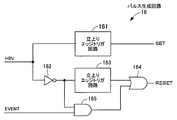
- FIG. 2 is a circuit diagram showing an example of a pulse generation circuit
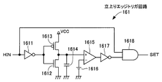
- FIG. 3 is a circuit diagram showing an example of a rising edge trigger circuit
- FIG. It is a circuit diagram which shows an example of an electric potential determination circuit.
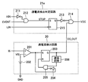
- FIG. 5 is a circuit diagram illustrating an example of an overcurrent detection circuit and an overcurrent detection determination circuit of the semiconductor device according to the first embodiment
- FIG. 6 is a timing chart illustrating a main part waveform during the switching operation of the semiconductor device. .
- the same symbol may be used for the terminal name and the voltage and signal at the terminal.
- the semiconductor device according to the first embodiment controls and drives the motor 10, and the semiconductor device shown in FIG. 1 uses AC power for one phase when the motor 10 is, for example, a three-phase induction motor. Only the output part is shown.
- This semiconductor device has a high-side power device HQ and a low-side power device LQ that are totem-pole connected.
- each of the high-side power device HQ and the low-side power device LQ is composed of an N-channel power MOSFET (Metal Oxide Semiconductor Field Effect Transistor).
- the high-side power device HQ and the low-side power device LQ may be other power devices such as IGBT (Insulated Gate Bipolar Transistor).
- the drain of the high-side power device HQ is connected to the positive terminal of the high-voltage power supply 11, and the negative terminal of the high-voltage power supply 11 is connected to the ground GND.
- the source of the low-side power device LQ is connected to the ground GND via a resistor RLQ.
- a connection point between the source of the high-side power device HQ and the drain of the low-side power device LQ, that is, the midpoint of the totem pole is connected to the motor 10.
- the gate of the high side power device HQ is connected to the output terminal HO of the high side drive circuit 12, and the gate of the low side power device LQ is connected to the output terminal LO of the low side drive circuit 13.
- the high-side drive circuit 12 has a reference potential terminal connected to the midpoint of the totem pole and the negative terminal of the high-side power supply 14, and a power supply terminal connected to the positive terminal of the high-side power supply 14.
- the reference potential terminal of the low-side drive circuit 13 is connected to the ground GND and the negative terminal of the low-side power supply 15, and the power supply terminal is connected to the positive terminal of the low-side power supply 15.
- the low side power supply potential is indicated by VCC with reference to the ground GND
- the high side reference potential and the high side power supply potential are indicated by VS and VB with respect to the ground GND, respectively.
- the semiconductor device also includes a pulse generation circuit 16, a level shift circuit 17, a high side potential detection circuit 18, a high side potential determination circuit 19, an overcurrent detection circuit 20, and an overcurrent detection determination circuit 21. ing.
- the pulse generation circuit 16 receives a logic input signal (high side logic signal) HIN for high side control from the outside, and generates a set signal SET and a reset signal RESET. Specifically, as shown in FIG. 2, the pulse generation circuit 16 includes a rising edge trigger circuit 161 that inputs a logic input signal HIN and outputs a set signal SET. The pulse generation circuit 16 also includes an inverter 162, a rising edge trigger circuit 163, an OR circuit 164, and an AND circuit 165. The input of the inverter 162 is connected to the input terminal of the logic input signal HIN, and the output of the inverter 162 is connected to the input of the rising edge trigger circuit 163 and one input of the AND circuit 165.
- the output of the rising edge trigger circuit 163 is connected to one input of the OR circuit 164, and the output of the OR circuit 164 constitutes the output terminal RESET of the reset signal RESET.
- the other input of the AND circuit 165 is connected to the input terminal of the event signal EVENT output from the high side potential determination circuit 19, and the output of the AND circuit 165 is connected to the other input of the OR circuit 164.
- the rising edge trigger circuit 161 includes an inverter 1611 whose input is connected to the input terminal of the logic input signal HIN.
- the output of the inverter 1611 is connected to the gates of the nMOS transistor 1612 and the pMOS transistor 1613.
- the source of the nMOS transistor 1612 is connected to the ground GND, and the drain of the nMOS transistor 1612 is connected to the drain of the pMOS transistor 1613.
- the source of the pMOS transistor 1613 is connected to the positive terminal of the low-side power supply 15 that supplies the low-side power supply potential VCC.
- the output of the inverter circuit composed of the nMOS transistor 1612 and the pMOS transistor 1613 is connected to one end of a capacitor 1614, and the other end of the capacitor 1614 is connected to the ground GND.
- the output of the inverter circuit is also connected to the non-inverting input of the comparator 1615.
- the inverting input of the comparator 1615 is connected to the positive terminal of the reference voltage source 1616, and the negative terminal of the reference voltage source 1616 is connected to the ground GND.
- the output of the comparator 1615 is connected to the input of the inverter 1617, the output of the inverter 1617 is connected to one input of the AND circuit 1618, and the other input of the AND circuit 1618 is connected to the input terminal of the logic input signal HIN. Has been.
- the output of the AND circuit 1618 constitutes an output terminal that outputs a set signal SET.
- the rising edge trigger circuit 163 has the same configuration. Accordingly, FIG. 3 will be referred to in the following description of the operation of the rising edge trigger circuit 163.
- the input of the rising edge trigger circuit 163 is a signal obtained by logically inverting the logic input signal HIN, and the output is a reset signal RESET via the OR circuit 164.
- the level shift circuit 17 has high breakdown voltage nMOS transistors HVN1 and HVN2, resistors LSR1 and LSR2, and clamping diodes D1 and D2.
- the gates of the nMOS transistors HVN1 and HVN2 are connected to the set signal output terminal SET and the reset signal output terminal RESET of the pulse generation circuit 16, respectively.
- the drains of the nMOS transistors HVN1 and HVN2 are connected to one ends of the resistors LSR1 and LSR2, respectively, and the other ends of the resistors LSR1 and LSR2 are connected to the high side power supply potential VB of the high side drive circuit 12.
- connection point between the drains of the nMOS transistors HVN1 and HVN2 and the resistors LSR1 and LSR2 is connected to the input terminal of the high-side drive circuit 12 and to the cathode terminals of the diodes D1 and D2.
- the anode terminals of the diodes D1 and D2 are connected to the high-side reference potential VS of the high-side drive circuit 12, that is, the midpoint of the totem pole.
- the sources of the nMOS transistors HVN1 and HVN2 are connected to the ground GND.
- the high-side potential detection circuit 18 detects a high-side potential, in the illustrated example, a high-side reference potential VS.
- a resistive field plate (RFP: Resistant Field Field Plate) is used as detection means. ).
- This resistive field plate is formed for the purpose of electric field relaxation in a high-voltage region HVJT (High Voltage-Junction-Terminal) in a high-voltage circuit device of a high-side circuit (for example, see International Publication No. 2013/0669408). ).
- One terminal of the resistive field plate is connected to the midpoint of the totem pole, and the other terminal is connected to the ground GND.
- the high-side potential detection circuit 18 divides the resistive field plate into two resistors RFP1 and RFP2 by providing a branch point in the resistive field plate, and the branch point of the resistive field plate is connected to the input terminal of the high-side potential determination circuit 19.
- a detection signal SENSE representing a change in the high side reference potential VS is output.
- the high side potential determination circuit 19 receives the detection signal SENSE detected by the high side potential detection circuit 18 and generates an event signal EVENT according to the change of the high side reference potential VS. As shown in FIG. 4, the high-side potential determination circuit 19 includes two protection diodes 191 and 192, a comparator 193, a reference voltage source 194, an inverter 195, and a rising edge trigger circuit 196. ing. The high side potential determination circuit 19 is installed on the low side potential side with respect to the potential of the ground GND together with the high side potential detection circuit 18.
- the input terminal of the detection signal SENSE is connected to the cathode of the protection diode 191, the anode of the protection diode 192, and the inverting input of the comparator 193.
- the anode of the protection diode 191 is connected to the ground GND, and the cathode of the protection diode 192 is connected to the low side power supply potential VCC.
- the non-inverting input of the comparator 193 is connected to the positive terminal of the reference voltage source 194, and the negative terminal of the reference voltage source 194 is connected to the ground GND.
- the output of the comparator 193 is connected to the input of the rising edge trigger circuit 196 via the inverter 195, and the output of the rising edge trigger circuit 196 constitutes an output terminal for outputting the event signal EVENT.
- the rising edge trigger circuit 196 has the same circuit configuration as that of the rising edge trigger circuit 161 shown in FIG. 3, and therefore, the following description of the operation of the rising edge trigger circuit 196 will be made with reference to FIG. .
- the input of the rising edge trigger circuit 196 becomes an inverted signal of the output signal MPLS of the comparator 193, and the output becomes the event signal EVENT.
- the overcurrent detection circuit 20 receives the current signal IS indicating the current value of the main current flowing through the low-side power device LQ, and outputs the overcurrent detection signal OC_OUT when the current signal IS exceeds a predetermined current value.
- the overcurrent detection circuit 20 includes a comparator 201, a reference voltage source 202, an RS flip-flop 203, an inverter 204, an AND circuit 205, and a delay circuit 206. .
- the comparator 201 has its non-inverting input connected to the connection point between the source of the low-side power device LQ and the resistor RLQ, and receives the current signal IS.
- the inverting input of the comparator 201 is connected to the positive terminal of the reference voltage source 202, and the negative terminal of the reference voltage source 202 is connected to the ground GND.
- the output of the comparator 201 is connected to the set terminal of the RS flip-flop 203 and the input of the inverter 204.
- the output of the inverter 204 is connected to one input of the AND circuit 205, and the output of the AND circuit 205 is connected to the reset terminal of the RS flip-flop 203.
- the output terminal of the RS flip-flop 203 is connected to the input of the delay circuit 206, and the output of the delay circuit 206 is connected to the other input of the AND circuit 205.
- the output terminal of the RS flip-flop 203 constitutes the output terminal of the overcurrent detection circuit 20 that outputs the overcurrent detection signal OC_OUT, and is connected to the overcurrent detection determination circuit 21.
- the overcurrent detection determination circuit 21 has input terminals for an overcurrent detection signal OC_OUT, an event signal EVENT, and a logic input signal HIN for high side control, and an output terminal for the overcurrent signal VOC. .
- the overcurrent detection determination circuit 21 includes an inverter 211, an AND circuit 212, an inverter 213, and an AND circuit 214 as shown in FIG.
- the inverter 211 receives a logic input signal HIN for high side control at its input, and the output of the inverter 211 is connected to one input of the AND circuit 212.
- the event signal EVENT is input to the other input of the AND circuit 212, and the signal STOP is output from the output of the AND circuit 212.
- the output of the AND circuit 212 is connected to the input of the inverter 213, and the output of the inverter 213 is connected to one input of the AND circuit 214.
- the other input of the AND circuit 214 receives the overcurrent detection signal OC_OUT from the overcurrent detection circuit 20, and the output of the AND circuit 214 constitutes the output terminal of the overcurrent detection determination circuit 21 to output the overcurrent signal VOC. To do.
- the output of the overcurrent detection determination circuit 21 is connected to the low side drive circuit 13.
- the low side drive circuit 13 outputs a low side output signal LO to the output terminal LO based on an external logic input signal (low side logic signal) LIN and an overcurrent signal VOC from the overcurrent detection determination circuit 21.
- a logic input signal HIN for high side control is input to the pulse generation circuit 16 and the overcurrent detection determination circuit 21, and a logic input signal LIN for low side control is input to the low side drive circuit 13.
- the logic input signal HIN and the logic input signal LIN are set with dead time so that the high-side power device HQ and the low-side power device LQ are not turned on at the same time.
- the rising edge trigger circuit 161 When the logic input signal HIN is input, in the pulse generation circuit 16, the rising edge trigger circuit 161 outputs the set signal SET triggered by the rising edge of the logic input signal HIN (high (H on the rising edge of HIN in FIG. 6). ) See SET for level). That is, in the rising edge trigger circuit 161 of FIG. 3, when the logic input signal HIN is at the low (L) level, the output of the inverter 1611 is at the H level, and the nMOS transistor 1612 is turned on (the pMOS transistor 1613 is turned off). ing. Thereby, since the electric charge of the capacitor 1614 is discharged, the output of the comparator 1615 becomes L level and the output of the inverter 1617 becomes H level.
- the AND circuit 1618 since the logic input signal HIN is L level, the AND circuit 1618 becomes L level.
- the set signal SET is output.
- the AND circuit 1618 receiving the H level from the inverter 1617 outputs an H level set signal SET.
- the output of the inverter 1611 becomes L level
- the pMOS transistor 1613 is turned on (the nMOS transistor 1612 is turned off), and the capacitor 1614 is charged.
- the output of the comparator 1615 becomes H level and the output of the inverter 1617 becomes L level.
- the AND circuit 1618 blocks the logic input signal HIN at the H level and outputs the set signal SET at the L level. That is, the set signal SET is output as a pulse signal having a predetermined time width.
- the nMOS transistor HVN1 of the level shift circuit 17 When the H level set signal SET is output, the nMOS transistor HVN1 of the level shift circuit 17 is turned on, and the connection point between the resistor LSR1 and the nMOS transistor HVN1 is lowered to the level of the ground GND.
- the high-side drive circuit 12 detects the level drop, the high-side output signal HO enters a high potential state with the high-side reference potential VS as a reference.
- the high side power device HQ transitions to an on state (at this time, the low side power device LQ is in an off state), and the high side reference potential VS is increased to supply current to the motor 10.
- an H level detection signal SENSE is input from the high side potential detection circuit 18 to the high side potential determination circuit 19 and the output signal MPLS of the comparator 193 becomes L level.
- the output of inverter 195 transitions to the H level. This transition is detected by the rising edge trigger circuit 196, and an event signal EVENT having a pulse width of a predetermined time is output.
- the event signal EVENT generated while the logic input signal HIN is at the H level since the output of the inverter 162 in FIG. 2 is at the L level, it is not involved in the control of the high side power device HQ.
- the pulse generation circuit 16 resets the rising edge trigger circuit 163 triggered by the rising edge of the inverted signal of the logic input signal HIN output from the inverter 162.
- the signal RESET is output. That is, the pulse generation circuit 16 generates the reset signal RESET indicated by a broken line in FIG. 6 using the falling edge of the logic input signal HIN as a trigger.
- the reset signal RESET is changed to the high-side drive circuit 12.
- the reset signal RESET indicated by a broken line. The broken line indicates that it was not actually generated).
- the output signal MPLS of the comparator 193 once becomes H level.
- the rising edge trigger circuit 196 outputs an H level event signal EVENT having a pulse width of a predetermined time. Since the logic input signal HIN is L level and the output of the inverter 162 is H level, the pulse generation circuit 16 receives the H level event signal EVENT, so that the output of the AND circuit 165 becomes H level.
- the H level reset signal RESET is output from the OR circuit 164.
- the high-side output signal HO of the high-side drive circuit 12 changes to the L level at time t2, and the high-side power device HQ is turned off.
- the high side reference potential VS becomes the level of the ground GND, and the output signal MPLS of the comparator 193 of the high side potential determination circuit 19 becomes the H level.
- the logic input signal HIN has transitioned to the L level
- the high side output signal HO has transitioned to the L level at the time t2 with a delay from the time t1, but during that time, the set dead time
- the logic input signal LIN may be input.
- FIG. 6 shows exactly that case. At this time, the high-side power device HQ and the low-side power device LQ are simultaneously turned on, and an overcurrent flows.
- the current ILQ that is the main current flowing through the low-side power device LQ is monitored by the overcurrent detection circuit 20.
- the overcurrent detection circuit 20 when the current signal IS corresponding to the current ILQ exceeds an overcurrent detection threshold determined by the voltage VIS of the reference voltage source 202, the comparator 201 outputs an H-level overcurrent detection state signal.
- the signal is held by the RS flip-flop 203 and becomes an overcurrent detection signal OC_OUT.
- the overcurrent detection signal OC_OUT is sent to the overcurrent detection determination circuit 21.
- the overcurrent detection signal OC_OUT is also input to the delay circuit 206, and the delay circuit 206 outputs an H level signal after a predetermined delay time has elapsed. Thereby, after the RS flip-flop 203 holds the overcurrent detection state, even when the overcurrent detection state is canceled (the output of the comparator 201 is at L level), until a predetermined delay time elapses, The overcurrent detection state is maintained.
- the logical input signal HIN and the event signal EVENT inverted by the inverter 211 are input to the AND circuit 212. Since the logic input signal HIN after the low side output signal LO is H level is L level and the event signal EVENT is H level, the signal STOP output from the AND circuit 212 becomes H level. Therefore, an L level signal obtained by inverting the signal STOP by the inverter 213 is input to the AND circuit 214.
- the AND circuit 214 receives the overcurrent detection signal OC_OUT from the overcurrent detection circuit 20, but the overcurrent detection signal OC_OUT is blocked by the signal STOP and is invalid. Therefore, the overcurrent signal VOC that is the output of the AND circuit 214 is held at the L level without becoming the H level.
- the AND circuit 214 passes the overcurrent detection signal OC_OUT from the overcurrent detection circuit 20. As a result, the overcurrent signal VOC becomes H level, and the generation of the overcurrent is transmitted to the low side drive circuit 13.
- the overcurrent detection signal OC_OUT is invalidated. That is, even if the overcurrent detection circuit 20 detects an overcurrent, the overcurrent detection determination circuit 21 invalidates the overcurrent detection signal OC_OUT and maintains the L level of the overcurrent signal VOC.
- FIG. 7 is a circuit diagram showing a semiconductor device according to the second embodiment
- FIG. 8 is a circuit diagram showing an example of an overcurrent detection circuit and an overcurrent detection determination circuit of the semiconductor device according to the second embodiment.
- FIGS. 1 and 5 are denoted by the same reference numerals, and detailed description thereof is omitted.
- the high side potential detection circuit 18 and the overcurrent detection determination circuit 21 of the semiconductor device according to the first embodiment are detected by high side potential detection.
- the circuit 18a and the overcurrent detection determination circuit 21a are changed.
- the high-side potential detection circuit 18a detects the high-side power supply potential VB as the high-side potential.
- the high-side power supply potential VB is obtained by shifting the high-side reference potential VS by the potential of the high-side power supply 14, and changes in the same manner following the high-side reference potential VS. Therefore, even if the high side potential detection circuit 18a monitors the high side power supply potential VB, the high side reference potential VS is monitored.
- the high-side potential detection circuit 18a has an NPN-type bipolar transistor 181, and its emitter is connected to the line of the high-side power supply potential VB.
- the base of the bipolar transistor 181 is connected to the positive terminal of the voltage source 182, and the negative terminal of the voltage source 182 is connected to the ground GND.
- the collector of the bipolar transistor 181 is connected to one end of the resistor 183, the other end of the resistor 183 is connected to the positive terminal of the voltage source 184, and the negative terminal of the voltage source 184 is connected to the ground GND.
- the collector of the bipolar transistor 181 constitutes the output of the high side potential detection circuit 18a and outputs a detection signal SENSE.
- the bipolar transistor 181 has a reverse breakdown voltage between the base and emitter corresponding to the high breakdown voltage of the high side circuit.
- the bipolar transistor 181 detects it. That is, normally, the potential of the high-side power supply 14 higher than the potential of the voltage source 182 is applied to the emitter of the bipolar transistor 181 even if the high-side power supply potential VB is the lowest. Therefore, the bipolar transistor 181 is in an off state, and a signal having a potential level of the voltage source 184 is output as the detection signal SENSE.
- the bipolar transistor 181 When the high-side reference potential VS fluctuates and the high-side power supply potential VB further falls below the potential obtained by subtracting the forward potential between the base and emitter of the bipolar transistor 181 from the potential of the voltage source 182, the bipolar transistor 181 is turned on. Transition to. As a result, the high side potential detection circuit 18a outputs an L level detection signal SENSE. Thereafter, when the high-side power supply potential VB returns to normal, the detection signal SENSE becomes the potential level of the voltage source 184 again.
- the overcurrent detection determination circuit 21a has input terminals for an overcurrent detection signal OC_OUT, an event signal EVENT, and logic input signals HIN and LIN, and an output terminal for the overcurrent signal VOC.
- the overcurrent detection determination circuit 21a has an RS flip-flop 215 added to the overcurrent detection determination circuit 21 of FIG. That is, the RS flip-flop 215 is arranged between the AND circuit 212 and the inverter 213, the set terminal is connected to the output of the AND circuit 212, and the reset terminal receives the logic input signal LIN for low side control. It is configured.
- the overcurrent detection determination circuit 21 a holds the signal STOP output from the AND circuit 212 by the RS flip-flop 215, and the RS flip-flop 215 outputs an H level signal to the inverter 213 during that time.
- the inverter 213 outputs an L level signal to one input of the AND circuit 214, so that the AND circuit 214 invalidates the overcurrent detection signal OC_OUT from the overcurrent detection circuit 20. That is, the AND circuit 214 blocks the passage of the overcurrent detection signal OC_OUT and outputs the L-level overcurrent signal VOC to the low side drive circuit 13.
- the signal STOP is held by the RS flip-flop 215 until the timing when the logic input signal LIN next becomes L level. That is, when the RS flip-flop 215 is reset by the fall of the logic input signal LIN for low side control, the RS flip-flop 215 outputs an L level signal to the inverter 213. As a result, the inverter 213 outputs an H level signal to one input of the AND circuit 214, so that the AND circuit 214 validates the overcurrent detection signal OC_OUT from the overcurrent detection circuit 20. That is, the AND circuit 214 can output the H-level overcurrent signal VOC to the low-side drive circuit 13.
- the overcurrent detection determination circuit 21a outputs an H-level overcurrent signal VOC, and the protection function of the low-side drive circuit 13 is activated, and the low-side power device LQ is activated. It returns to a state where it can be turned off.
- overcurrent detection is disabled during the half cycle of the logic input signal LIN for low side control, but the reset signal RESET generated by the high side power device HQ by the event signal EVENT is used. Therefore, the upper and lower arm short circuit currents do not continue to flow.
- the overcurrent detection determination circuit 21a generates a pulse when the delay time of the delay circuit 206 is long to some extent (for example, longer than the pulse width of the event signal EVENT) or when external noise is generated again after the end of the signal STOP. This is particularly useful in applications where there may be situations where the generator circuit 16 generates the reset signal RESET again.
Landscapes
- Engineering & Computer Science (AREA)
- Power Engineering (AREA)
- Microelectronics & Electronic Packaging (AREA)
- Computer Hardware Design (AREA)
- Electronic Switches (AREA)
- Inverter Devices (AREA)
Abstract
ハイサイドのパワーデバイスをオフ状態にするタイミングが遅れることで上下アーム短絡が発生するようなことがあっても、システムとして動作を継続できるようにする。 ハイサイド電位検出回路(18)により検出されたハイサイド基準電位(VS)が立上るとハイサイド電位判定回路(19)がイベント信号(EVENT)を出力し、そのとき論理入力信号(HIN)がLレベルであるとパルス生成回路(16)がハイサイド駆動回路(12)に対するリセット信号(RESET)を再生成する。過電流検出判定回路(21)は、ハイサイド制御用の論理入力信号(HIN)がLレベルのとき、イベント信号(EVENT)が入力されると過電流検出回路(20)からの過電流検出信号(OC_OUT)を無効にした過電流信号(VOC)を出力し、イベント信号(EVENT)が入力されていないと過電流検出信号(OC_OUT)を有効とする。
Description
本発明は、トーテムポール接続された2つのパワーデバイスに過電流が流れたことを検出する過電流保護機能を備えた半導体装置に関する。
インバータまたはコンバータにおいては、パワーデバイスをトーテムポール接続し、ハイサイドおよびローサイドのパワーデバイスをそれぞれ駆動回路によって駆動する回路構成が採られている。すなわち、ハイサイドでは、パルス生成回路によってグランド電位を基準に生成された信号は、レベルシフト回路でレベルシフトされてからハイサイド駆動回路に伝達され、ハイサイドのパワーデバイスをオン・オフ駆動する。一方、ローサイドでは、グランド電位を基準に生成された信号がローサイド駆動回路に伝達され、ローサイドのパワーデバイスをオン・オフ駆動する。
ローサイドのパワーデバイスとハイサイドのパワーデバイスとの接続点であるトーテムポールの中点は、モータ等の誘導性負荷に接続される。そのため、そのトーテムポールの中点に誘導性負荷、寄生インダクタンス等に起因する外来ノイズが重畳されてしまうことがある。このようなとき、ノイズの大きさやタイミング等によっては、トーテムポールの中点電位がオーバーシュートやアンダーシュート状態となる。すなわち、トーテムポールの中点電位は、ハイサイドのパワーデバイスの高圧電位以上の電位になったり、グランド電位以下の電位になったりする。
トーテムポールの中点電位がグランド電位よりも低くなるタイミングのときに、パルス生成回路からハイサイドのパワーデバイスにオフ信号が出力されるようなことがある。その場合、ハイサイドでは、レベルシフト回路がその信号を正常にハイサイド駆動回路に伝達することができなくなってしまう。すると、ハイサイドのパワーデバイスは、オフすべきタイミングのときにオフできずにオンのままとなり、本来のスイッチング機能を維持することができなくなってしまう。
ここで、オフすべきタイミングにオフすることができなくなることに対処した技術(たとえば、特許文献1参照)が知られている。特許文献1の技術によれば、第1のオフ信号を出力してから所定時間経過後に第2のオフ信号を出力するようにしている。これにより、第1のオフ信号がレベルシフト回路を正常に伝達することができなかったとしても、第2のオフ信号がレベルシフト回路を正常に伝達することにより、機能的な誤動作を回避している。
ただし、この特許文献1の技術では、第1および第2のオフ信号を単に一定の間隔で機械的に出力しているだけである。そのため、所定時間経過した時点でも新たな外来ノイズが発生する可能性はあるので、本質的に誤動作を完全に回避することはできない。
そこで、レベルシフト回路がハイサイドのパワーデバイスをオフ状態にするリセット信号を正常に伝達していないことを判定して第2のリセット信号を再生成することが提案されている(たとえば、特許文献2参照)。特許文献2に記載の半導体装置は、ハイサイド電位を検出するハイサイド電位検出回路と、ハイサイド電位検出回路が検出したハイサイド電位の変化に基づきイベント信号を出力するハイサイド電位判定回路とを備えている。この半導体装置では、ハイサイド電位判定回路が出力したイベント信号と外部から入力された論理入力信号とに応じて、パルス生成回路がリセット信号を再生成するようにしている。すなわち、ハイサイド電位判定回路は、ハイサイド電位検出回路が検出したハイサイド電位(基準電位または電源電位)を監視し、レベルシフト回路におけるリセット信号の伝達を阻害するようなハイサイド電位の変動であると判定すると、イベント信号を出力する。ここで、パルス生成回路は、ハイサイド電位判定回路からイベント信号を受けているタイミングとリセット信号の生成のタイミングとが重なった場合、リセット信号を再生成する。このように、外来ノイズによりリセット信号の伝達が阻害されるようなことがあると、リセット信号を再生成することになるので、ハイサイドのパワーデバイスは、確実にオフされる。
特許文献2に記載の半導体装置では、ハイサイドのパワーデバイスをオフするリセットのタイミングのときに、リセット信号の伝達が阻害され得ることを示すイベント信号が出力されているとリセット信号を再生成する。これにより、ハイサイドのパワーデバイスを確実にオフさせる。しかしながら、トーテムポール接続しているパワーデバイスのデッドタイム(上下アーム短絡を防止するためにある、一方がオフしてから他方がオンするまでの遅延時間)が短い場合、また、外来ノイズの影響が無視できない場合やハイサイド電位の変動期間が長い場合等、正規のタイミングから遅れてオフ信号が出力されることがある。このような場合、ハイサイドをオフするまでにローサイドのパワーデバイスがオンすることになる。この結果、上下アーム短絡が発生し、パワーデバイスに過電流が流れ、ローサイドの制御として過電流が検出されるので、意図していない動作停止を引き起こすという問題があった。
本発明はこのような点に鑑みてなされたものであり、ハイサイドのパワーデバイスをオフ状態にする信号が正規のタイミングから遅れることで上下アーム短絡が発生することがあっても、システムとして動作を継続できる半導体装置を提供することを目的とする。
本発明では上記の課題を解決するために、ハイサイド論理信号に基づいてトーテムポール接続のハイサイドパワーデバイスを駆動するハイサイド駆動回路と、ハイサイド電位を検出するハイサイド電位検出回路と、前記ハイサイド電位検出回路が検出した前記ハイサイド電位の変化に基づきイベント信号を出力するハイサイド電位判定回路と、ローサイド論理信号に基づいてトーテムポール接続のローサイドパワーデバイスを駆動するローサイド駆動回路と、前記ローサイドパワーデバイスの主電流の電流値を示す電流信号を入力して過電流を検出したときに前記ローサイドパワーデバイスをオフさせるための過電流検出信号を出力する過電流検出回路と、前記ハイサイド論理信号および前記イベント信号に基づいて前記過電流検出信号を前記ローサイド駆動回路に伝達するかどうかを判定する過電流検出判定回路と、を備え、前記過電流検出判定回路は、前記イベント信号の出力前に前記ローサイドパワーデバイスをオンすることで検出される前記過電流検出信号を無効にすることを特徴とする半導体装置が提供される。
このような半導体装置によれば、トーテムポール接続しているハイサイドパワーデバイスおよびローサイドパワーデバイスのデッドタイム設定が短い場合、ハイサイドを確実にオフするためのイベント信号の出力前に、ローサイドパワーデバイスがオンし、上下アーム短絡が発生した結果、所定期間内に過電流を検出しても、ローサイド駆動回路を動作停止しないようにした。
上記構成の半導体装置は、ハイサイドパワーデバイスの再リセットが必要なときにローサイドパワーデバイスの過電流を検出した場合、その検出を無効にしたので、不必要な動作停止およびアラーム信号を出すことなく動作を継続させることができるという利点がある。
本発明の上記および他の目的、特徴および利点は、本発明の例として好ましい実施の形態を表す添付の図面と関連した以下の説明により明らかになるであろう。
以下、本発明の実施の形態について、図面を参照して詳細に説明する。
<第1の実施の形態>
図1は第1の実施の形態に係る半導体装置を示す回路図、図2はパルス生成回路の一例を示す回路図、図3は立上りエッジトリガ回路の一例を示す回路図、図4はハイサイド電位判定回路の一例を示す回路図である。図5は第1の実施の形態に係る半導体装置の過電流検出回路および過電流検出判定回路の一例を示す回路図、図6は半導体装置のスイッチング動作時における要部波形を示すタイミングチャートである。なお、以下の説明において、端子名とその端子における電圧、信号等は、同じ符号を用いることがある。
<第1の実施の形態>
図1は第1の実施の形態に係る半導体装置を示す回路図、図2はパルス生成回路の一例を示す回路図、図3は立上りエッジトリガ回路の一例を示す回路図、図4はハイサイド電位判定回路の一例を示す回路図である。図5は第1の実施の形態に係る半導体装置の過電流検出回路および過電流検出判定回路の一例を示す回路図、図6は半導体装置のスイッチング動作時における要部波形を示すタイミングチャートである。なお、以下の説明において、端子名とその端子における電圧、信号等は、同じ符号を用いることがある。
第1の実施の形態に係る半導体装置は、モータ10を制御駆動するものであって、図1に示す半導体装置は、モータ10をたとえば三相誘導モータとしたときの一相分の交流電力を出力する部分のみを示している。
この半導体装置は、トーテムポール接続されたハイサイドパワーデバイスHQおよびローサイドパワーデバイスLQを有している。この実施の形態では、ハイサイドパワーデバイスHQおよびローサイドパワーデバイスLQは、それぞれNチャネルのパワーMOSFET(Metal Oxide Semiconductor Field Effect Transistor)で構成している。なお、ハイサイドパワーデバイスHQおよびローサイドパワーデバイスLQは、IGBT(Insulated Gate Bipolar Transistor)のような他のパワーデバイスであってもよい。
ハイサイドパワーデバイスHQのドレインは、高圧電源11の正極端子に接続され、高圧電源11の負極端子は、グランドGNDに接続されている。ローサイドパワーデバイスLQのソースは、抵抗RLQを介してグランドGNDに接続されている。ハイサイドパワーデバイスHQのソースとローサイドパワーデバイスLQのドレインとの接続点、すなわち、トーテムポールの中点は、モータ10に接続されている。
ハイサイドパワーデバイスHQのゲートは、ハイサイド駆動回路12の出力端子HOに接続され、ローサイドパワーデバイスLQのゲートは、ローサイド駆動回路13の出力端子LOに接続されている。ハイサイド駆動回路12は、その基準電位端子がトーテムポールの中点およびハイサイド電源14の負極端子に接続され、電源端子がハイサイド電源14の正極端子に接続されている。ローサイド駆動回路13は、その基準電位端子がグランドGNDおよびローサイド電源15の負極端子に接続され、電源端子がローサイド電源15の正極端子に接続されている。ここで、ローサイド電源電位は、グランドGNDを基準としたVCCで示され、ハイサイド基準電位およびハイサイド電源電位は、それぞれグランドGNDを基準としたVS,VBで示している。
半導体装置は、また、パルス生成回路16と、レベルシフト回路17と、ハイサイド電位検出回路18と、ハイサイド電位判定回路19と、過電流検出回路20と、過電流検出判定回路21とを備えている。
パルス生成回路16は、外部からハイサイド制御用の論理入力信号(ハイサイド論理信号)HINを入力し、セット信号SETおよびリセット信号RESETを生成する。具体的には、図2に示したように、パルス生成回路16は、論理入力信号HINを入力し、セット信号SETを出力する立上りエッジトリガ回路161を備えている。パルス生成回路16は、また、インバータ162と、立上りエッジトリガ回路163と、OR回路164と、AND回路165とを備えている。インバータ162の入力は、論理入力信号HINの入力端子に接続され、インバータ162の出力は、立上りエッジトリガ回路163の入力とAND回路165の一方の入力とに接続されている。立上りエッジトリガ回路163の出力は、OR回路164の一方の入力に接続され、OR回路164の出力は、リセット信号RESETの出力端子RESETを構成している。AND回路165の他方の入力は、ハイサイド電位判定回路19から出力されるイベント信号EVENTの入力端子に接続され、AND回路165の出力は、OR回路164の他方の入力に接続されている。
立上りエッジトリガ回路161は、図3に示したように、入力が論理入力信号HINの入力端子に接続されたインバータ1611を備えている。このインバータ1611の出力は、nMOSトランジスタ1612およびpMOSトランジスタ1613のゲートに接続されている。nMOSトランジスタ1612のソースは、グランドGNDに接続され、nMOSトランジスタ1612のドレインは、pMOSトランジスタ1613のドレインに接続されている。pMOSトランジスタ1613のソースは、ローサイド電源電位VCCを供給するローサイド電源15の正極端子に接続されている。nMOSトランジスタ1612およびpMOSトランジスタ1613からなるインバータ回路の出力は、コンデンサ1614の一端に接続され、コンデンサ1614の他端は、グランドGNDに接続されている。インバータ回路の出力は、また、比較器1615の非反転入力に接続されている。比較器1615の反転入力には、基準電圧源1616の正極端子が接続され、基準電圧源1616の負極端子は、グランドGNDに接続されている。比較器1615の出力は、インバータ1617の入力に接続され、インバータ1617の出力は、AND回路1618の一方の入力に接続され、AND回路1618の他方の入力は、論理入力信号HINの入力端子に接続されている。AND回路1618の出力は、セット信号SETを出力する出力端子を構成している。
なお、ここでは、立上りエッジトリガ回路161の具体例について説明したが、立上りエッジトリガ回路163においても、同じ構成を有している。したがって、以下の立上りエッジトリガ回路163の動作説明には、図3を参照することにする。立上りエッジトリガ回路163の入力は、論理入力信号HINを論理反転した信号となり、出力は、OR回路164を介してリセット信号RESETとなる。
レベルシフト回路17は、高耐圧のnMOSトランジスタHVN1,HVN2と、抵抗LSR1,LSR2と、クランプ用のダイオードD1,D2とを有している。nMOSトランジスタHVN1,HVN2のゲートは、それぞれパルス生成回路16のセット信号出力端子SETおよびリセット信号出力端子RESETに接続されている。nMOSトランジスタHVN1,HVN2のドレインは、それぞれ抵抗LSR1,LSR2の一端に接続され、抵抗LSR1,LSR2の他端は、ハイサイド駆動回路12のハイサイド電源電位VBに接続されている。nMOSトランジスタHVN1,HVN2のドレインと抵抗LSR1,LSR2との接続点は、それぞれハイサイド駆動回路12の入力端子に接続されるとともに、ダイオードD1,D2のカソード端子に接続されている。ダイオードD1,D2のアノード端子は、ハイサイド駆動回路12のハイサイド基準電位VS、すなわち、トーテムポールの中点に接続されている。nMOSトランジスタHVN1,HVN2のソースは、グランドGNDに接続されている。
ハイサイド電位検出回路18は、ハイサイドの電位、図示の例では、ハイサイド基準電位VSを検出するもので、第1の実施の形態では、検出手段として抵抗性フィールドプレート(RFP:Resistant Field Plate)を利用している。この抵抗性フィールドプレートは、ハイサイド回路の高耐圧領域デバイスにおいて、耐圧領域HVJT(High Voltage Junction Terminal)の電界緩和を目的に形成されているものである(たとえば、国際公開第2013/069408号参照)。抵抗性フィールドプレートの一方の端子は、トーテムポールの中点に接続され、他方の端子は、グランドGNDに接続されている。ハイサイド電位検出回路18は、抵抗性フィールドプレートに分岐点を設けて2つの抵抗RFP1,RFP2に分割し、抵抗性フィールドプレートの分岐点は、ハイサイド電位判定回路19の入力端子に接続され、ハイサイド基準電位VSの変化を表す検出信号SENSEを出力している。
ハイサイド電位判定回路19は、ハイサイド電位検出回路18が検出した検出信号SENSEを入力し、ハイサイド基準電位VSの変化に応じてイベント信号EVENTを生成する。このハイサイド電位判定回路19は、図4に示したように、2つの保護用ダイオード191,192と、比較器193と、基準電圧源194と、インバータ195と、立上りエッジトリガ回路196とを備えている。また、ハイサイド電位判定回路19は、ハイサイド電位検出回路18とともに、グランドGNDの電位を基準としたローサイドの電位側に設置されている。
ハイサイド電位判定回路19において、検出信号SENSEの入力端子は、保護用ダイオード191のカソードと、保護用ダイオード192のアノードと、比較器193の反転入力に接続されている。保護用ダイオード191のアノードは、グランドGNDに接続され、保護用ダイオード192のカソードは、ローサイド電源電位VCCに接続されている。比較器193の非反転入力は、基準電圧源194の正極端子に接続され、基準電圧源194の負極端子は、グランドGNDに接続されている。比較器193の出力は、インバータ195を介して立上りエッジトリガ回路196の入力に接続され、立上りエッジトリガ回路196の出力は、イベント信号EVENTを出力する出力端子を構成している。立上りエッジトリガ回路196は、図3に示した立上りエッジトリガ回路161と同じ回路構成を有しており、したがって、以下の立上りエッジトリガ回路196の動作説明には、図3を参照することにする。このとき、立上りエッジトリガ回路196の入力は、比較器193の出力信号MPLSの反転信号となり、出力は、イベント信号EVENTとなる。
過電流検出回路20は、ローサイドパワーデバイスLQに流れる主電流の電流値を示す電流信号ISを入力し、電流信号ISが所定の電流値を超えたときには、過電流検出信号OC_OUTを出力する。電流信号ISは、ローサイドパワーデバイスLQのソースとグランドGNDとの間に接続された抵抗RLQにより主電流の電流値を電圧に変換した信号(=電流値×抵抗RLQの抵抗値)で、過電流検出回路20に入力される。この過電流検出回路20は、図5に示したように、比較器201と、基準電圧源202と、RSフリップフロップ203と、インバータ204と、AND回路205と、遅延回路206とを備えている。
過電流検出回路20において、比較器201は、その非反転入力がローサイドパワーデバイスLQのソースと抵抗RLQとの接続点に接続されて、電流信号ISが入力される。比較器201の反転入力には、基準電圧源202の正極端子が接続され、基準電圧源202の負極端子は、グランドGNDに接続されている。比較器201の出力は、RSフリップフロップ203のセット端子およびインバータ204の入力に接続されている。インバータ204の出力は、AND回路205の一方の入力に接続され、AND回路205の出力は、RSフリップフロップ203のリセット端子に接続されている。RSフリップフロップ203の出力端子は、遅延回路206の入力に接続され、遅延回路206の出力は、AND回路205の他方の入力に接続されている。RSフリップフロップ203の出力端子は、また、過電流検出信号OC_OUTを出力する過電流検出回路20の出力端子を構成していて、過電流検出判定回路21に接続されている。
過電流検出判定回路21は、過電流検出信号OC_OUT、イベント信号EVENTおよびハイサイド制御用の論理入力信号HINのための入力端子を有し、過電流信号VOCのための出力端子を有している。
過電流検出判定回路21は、図5に示したように、インバータ211と、AND回路212と、インバータ213と、AND回路214とを備えている。インバータ211は、その入力にハイサイド制御用の論理入力信号HINを受け、インバータ211の出力は、AND回路212の一方の入力に接続されている。AND回路212の他方の入力には、イベント信号EVENTが入力され、AND回路212の出力から信号STOPが出力される。AND回路212の出力は、インバータ213の入力に接続され、インバータ213の出力は、AND回路214の一方の入力に接続されている。AND回路214の他方の入力は、過電流検出回路20からの過電流検出信号OC_OUTを受け、AND回路214の出力は過電流検出判定回路21の出力端子を構成して、過電流信号VOCを出力する。
過電流検出判定回路21の出力は、ローサイド駆動回路13に接続される。ローサイド駆動回路13は、外部からの論理入力信号(ローサイド論理信号)LINと過電流検出判定回路21からの過電流信号VOCとに基づいて出力端子LOにローサイド出力信号LOを出力する。
次に、以上の構成を有する半導体装置の動作について、図6のタイミングチャートを参照しながら説明する。まず、パルス生成回路16および過電流検出判定回路21には、ハイサイド制御用の論理入力信号HINが入力され、ローサイド駆動回路13には、ローサイド制御用の論理入力信号LINが入力されている。論理入力信号HINおよび論理入力信号LINは、ハイサイドパワーデバイスHQおよびローサイドパワーデバイスLQが同時にオン状態になることがないようにデッドタイムが設定されている。
論理入力信号HINが入力されると、パルス生成回路16では、立上りエッジトリガ回路161が論理入力信号HINの立上りエッジをトリガとしてセット信号SETを出力する(図6のHINの立上りエッジでハイ(H)レベルとなるSETを参照)。すなわち、図3の立上りエッジトリガ回路161では、論理入力信号HINがロー(L)レベルのとき、インバータ1611の出力がHレベルとなり、nMOSトランジスタ1612がオン状態(pMOSトランジスタ1613はオフ状態)になっている。これにより、コンデンサ1614の電荷が放電されているので、比較器1615の出力はLレベル、インバータ1617の出力はHレベルとなるが、論理入力信号HINがLレベルなので、AND回路1618は、Lレベルのセット信号SETを出力する。論理入力信号HINがHレベルになると、インバータ1617からHレベルを受けているAND回路1618は、Hレベルのセット信号SETを出力する。このとき、インバータ1611の出力がLレベルとなり、pMOSトランジスタ1613がオン状態(nMOSトランジスタ1612がオフ状態)になって、コンデンサ1614を充電する。コンデンサ1614の容量等によって決まる所定時間後にコンデンサ1614の充電電位が基準電圧源1616の電位を超えると、比較器1615の出力はHレベル、インバータ1617の出力はLレベルとなる。これにより、AND回路1618は、Hレベルの論理入力信号HINをブロックし、Lレベルのセット信号SETを出力する。つまり、セット信号SETは、所定時間幅を有するパルス信号で出力される。
Hレベルのセット信号SETが出力されると、レベルシフト回路17のnMOSトランジスタHVN1がオン状態となり、抵抗LSR1とnMOSトランジスタHVN1との接続点は、グランドGNDのレベルに低下する。ハイサイド駆動回路12がそのレベル低下を検出すると、ハイサイド出力信号HOは、ハイサイド基準電位VSを基準とする高電位状態になる。これにより、ハイサイドパワーデバイスHQは、オン状態(このとき、ローサイドパワーデバイスLQは、オフ状態にある)に遷移し、ハイサイド基準電位VSが高くなってモータ10に電流が供給される。このハイサイド基準電位VSが立上ると、Hレベルの検出信号SENSEがハイサイド電位検出回路18からハイサイド電位判定回路19に入力され、比較器193の出力信号MPLSは、Lレベルになる。これにより、インバータ195の出力は、Hレベルに遷移する。この遷移は、立上りエッジトリガ回路196によって検出され、所定時間のパルス幅を有するイベント信号EVENTが出力される。ただし、この論理入力信号HINがHレベルの期間に生成されるイベント信号EVENTに関しては、図2のインバータ162の出力がLレベルとなっているので、ハイサイドパワーデバイスHQの制御に何ら関与しない。
次に、論理入力信号HINがHレベルからLレベルになると、パルス生成回路16では、立上りエッジトリガ回路163が、インバータ162から出力される論理入力信号HINの反転信号の立上りエッジでトリガされてリセット信号RESETを出力する。すなわち、パルス生成回路16は、論理入力信号HINの立下りエッジをトリガとして、図6に破線で示したリセット信号RESETを生成する。
このとき、リセット信号RESETが出力されたタイミング(時刻t0)に外来ノイズの侵入により、ハイサイド基準電位VSがグランドGNDのレベル以下に低下することがあると、リセット信号RESETがハイサイド駆動回路12に正常に伝達できなくなる(破線で示したリセット信号RESET。破線は、実際には生成されなかったことを示す。)。この場合、ハイサイド基準電位VSがグランドGNDのレベル以下に低下すると、ハイサイド電位判定回路19では、比較器193の出力信号MPLSは、一旦Hレベルになる。その後、ハイサイド基準電位VSが回復して検出信号SENSEが基準電圧源194の基準電圧REF1より高くなると、比較器193の出力信号MPLSは、再びLレベルになり、インバータ195の出力は、Hレベルに遷移する。これにより、立上りエッジトリガ回路196から、所定時間のパルス幅を有するHレベルのイベント信号EVENTが出力される。論理入力信号HINがLレベルでインバータ162の出力がHレベルとなっているので、パルス生成回路16では、Hレベルのイベント信号EVENTが入力されることで、AND回路165の出力がHレベルになり、OR回路164からHレベルのリセット信号RESETが出力される。これにより、ハイサイド駆動回路12のハイサイド出力信号HOは、時刻t2でLレベルに遷移し、ハイサイドパワーデバイスHQがオフする。この結果、ハイサイド基準電位VSがグランドGNDのレベルになり、ハイサイド電位判定回路19の比較器193の出力信号MPLSがHレベルになる。
ここで、論理入力信号HINがLレベルに遷移したにも拘わらず、ハイサイド出力信号HOが時刻t1から遅れて時刻t2でLレベルに遷移しているが、その間に、設定されているデッドタイムによっては、論理入力信号LINが入力されてしまうことがある。図6では、正にその場合を示している。このとき、ハイサイドパワーデバイスHQおよびローサイドパワーデバイスLQは、同時にオン状態となり、過電流が流れることになる。
ローサイドパワーデバイスLQを流れる主電流である電流ILQは、過電流検出回路20によって監視されている。過電流検出回路20では、電流ILQに対応する電流信号ISが基準電圧源202の電圧VISによって定まる過電流検出閾値を超えると、比較器201は、Hレベルの過電流検状態信号を出力する。その信号は、RSフリップフロップ203により保持され、過電流検出信号OC_OUTとなる。この過電流検出信号OC_OUTは、過電流検出判定回路21に送られる。なお、過電流検出信号OC_OUTは、遅延回路206にも入力されており、遅延回路206は、所定の遅延時間の経過後に、Hレベルの信号を出力する。これにより、RSフリップフロップ203が過電流検出状態を保持した後、過電流検出状態が解除(比較器201の出力がLレベルに)された場合においても、所定の遅延時間が経過するまでは、過電流検出状態を保持するようにしている。
過電流検出判定回路21では、AND回路212に対しインバータ211によって反転された論理入力信号HINとイベント信号EVENTとが入力されている。ローサイド出力信号LOがHレベル後の論理入力信号HINはLレベル、イベント信号EVENTはHレベルであるので、AND回路212が出力する信号STOPは、Hレベルとなる。このため、AND回路214には、信号STOPがインバータ213で反転されたLレベルの信号が入力されることになる。このAND回路214は、過電流検出回路20から過電流検出信号OC_OUTが入力されているが、その過電流検出信号OC_OUTは、信号STOPにより阻止されて無効となっている。このため、AND回路214の出力である過電流信号VOCは、HレベルになることなくLレベルを保持する。なお、信号STOPが出力されていない(信号STOPがLレベルである)と、AND回路214は、過電流検出回路20からの過電流検出信号OC_OUTを通過させる。これにより、過電流信号VOCがHレベルとなり、ローサイド駆動回路13には、過電流の発生が伝達される。
つまり、論理入力信号HINがLレベルでイベント信号EVENTがHレベルであるとき、2回目のリセット信号RESET(図6において実線で示されるHレベルのパルス)と同じタイミングで信号STOPがHレベルの期間、過電流検出信号OC_OUTが無効にされる。すなわち、過電流検出判定回路21は、過電流検出回路20が過電流を検出しても、過電流検出信号OC_OUTを無効にして、過電流信号VOCのLレベルを維持する。
これにより、ハイサイドパワーデバイスHQをオフするまでにローサイドパワーデバイスLQがオンして過電流が発生したとしても、半導体装置として動作停止信号およびアラーム信号を出力させず、システムとして動作を継続させることを可能にしている。
図7は第2の実施の形態に係る半導体装置を示す回路図、図8は第2の実施の形態に係る半導体装置の過電流検出回路および過電流検出判定回路の一例を示す回路図である。この図7および図8において、図1および図5に示した構成要素と同じまたは均等の構成要素については同じ符号を付してその詳細な説明は省略する。
この第2の実施の形態に係る半導体装置は、図7に示したように、第1の実施の形態に係る半導体装置のハイサイド電位検出回路18および過電流検出判定回路21をハイサイド電位検出回路18aおよび過電流検出判定回路21aに変更している。
ハイサイド電位検出回路18aは、ハイサイド電位としてハイサイド電源電位VBを検出対象としている。このハイサイド電源電位VBは、ハイサイド基準電位VSをハイサイド電源14の電位の分だけシフトしたものであり、ハイサイド基準電位VSに追随して同じ変化をする。したがって、ハイサイド電位検出回路18aがハイサイド電源電位VBを監視しても、ハイサイド基準電位VSを監視していることになる。
ハイサイド電位検出回路18aは、NPN型のバイポーラトランジスタ181を有しており、そのエミッタは、ハイサイド電源電位VBのラインに接続されている。バイポーラトランジスタ181のベースは、電圧源182の正極端子に接続され、電圧源182の負極端子は、グランドGNDに接続されている。バイポーラトランジスタ181のコレクタは、抵抗183の一端に接続され、抵抗183の他端は、電圧源184の正極端子に接続され、電圧源184の負極端子は、グランドGNDに接続されている。バイポーラトランジスタ181のコレクタは、このハイサイド電位検出回路18aの出力を構成し、検出信号SENSEを出力する。バイポーラトランジスタ181は、そのベース-エミッタ間がハイサイド回路の高耐圧に相当する逆耐圧を有しているものとしている。
以上の構成により、ハイサイド基準電位VSが変動すると、それに追従してハイサイド電源電位VBが変動し、それをバイポーラトランジスタ181が検出する。すなわち、通常は、ハイサイド電源電位VBが最も低下したとしても電圧源182の電位よりも高いハイサイド電源14の電位がバイポーラトランジスタ181のエミッタに印加されている。そのため、バイポーラトランジスタ181はオフ状態にあり、検出信号SENSEとして、電圧源184の電位のレベルの信号が出力されている。
ハイサイド基準電位VSが変動して、ハイサイド電源電位VBが電圧源182の電位からバイポーラトランジスタ181のベース-エミッタ間の順方向電位を差し引いた電位よりもさらに低下すると、バイポーラトランジスタ181はオン状態に遷移する。これによって、ハイサイド電位検出回路18aは、Lレベルの検出信号SENSEを出力する。その後、ハイサイド電源電位VBが正常に戻ると、検出信号SENSEは再び電圧源184の電位のレベルとなる。
過電流検出判定回路21aは、過電流検出信号OC_OUT、イベント信号EVENT、および論理入力信号HINおよびLINのための入力端子を有し、過電流信号VOCのための出力端子を有している。
過電流検出判定回路21aは、図8に示したように、図5の過電流検出判定回路21と比較してRSフリップフロップ215が追加されている。すなわち、RSフリップフロップ215は、AND回路212とインバータ213との間に配置され、セット端子は、AND回路212の出力に接続され、リセット端子は、ローサイド制御用の論理入力信号LINを受けるように構成されている。
この過電流検出判定回路21aは、AND回路212が出力する信号STOPをRSフリップフロップ215によって保持し、その間、RSフリップフロップ215がHレベルの信号をインバータ213に出力する。これにより、インバータ213は、Lレベルの信号をAND回路214の一方の入力に出力するので、AND回路214は、過電流検出回路20からの過電流検出信号OC_OUTを無効にする。すなわち、AND回路214は、過電流検出信号OC_OUTの通過を阻止し、Lレベルの過電流信号VOCをローサイド駆動回路13に出力する。
RSフリップフロップ215による信号STOPの保持は、論理入力信号LINが次にLレベルとなるタイミングまでである。すなわち、RSフリップフロップ215がローサイド制御用の論理入力信号LINの立下がりによりリセットされると、RSフリップフロップ215がLレベルの信号をインバータ213に出力する。これにより、インバータ213は、Hレベルの信号をAND回路214の一方の入力に出力するので、AND回路214は、過電流検出回路20からの過電流検出信号OC_OUTを有効にする。すなわち、AND回路214は、Hレベルの過電流信号VOCをローサイド駆動回路13に出力できるようになる。これにより、過電流検出回路20が過電流を検出すると、過電流検出判定回路21aがHレベルの過電流信号VOCを出力し、ローサイド駆動回路13の保護機能が有効となってローサイドパワーデバイスLQをオフすることができる状態に戻される。
なお、この過電流検出判定回路21aでは、ローサイド制御用の論理入力信号LINの半周期の間、過電流検出を無効にしているが、ハイサイドパワーデバイスHQがイベント信号EVENTにより発生するリセット信号RESETで確実にオフするため、上下アーム短絡電流が流れ続けてしまうことはない。
また、この過電流検出判定回路21aは、遅延回路206の遅延時間がある程度長い場合(たとえば、イベント信号EVENTのパルス幅より長い場合)や、信号STOPの終了後に再度外来ノイズが発生して、パルス生成回路16が再々リセット信号RESETを生成するような状況があり得るアプリケーションに特に有用である。
上記については単に本発明の原理を示すものである。さらに、多数の変形、変更が当業者にとって可能であり、本発明は上記に示し、説明した正確な構成および応用例に限定されるものではなく、対応するすべての変形例および均等物は、添付の請求項およびその均等物による本発明の範囲とみなされる。また、各実施の形態は、矛盾のない範囲で複数の実施の形態を適宜組み合わせて実施することができる。
10 モータ
11 高圧電源
12 ハイサイド駆動回路
13 ローサイド駆動回路
14 ハイサイド電源
15 ローサイド電源
16 パルス生成回路
17 レベルシフト回路
18,18a ハイサイド電位検出回路
19 ハイサイド電位判定回路
20 過電流検出回路
21,21a 過電流検出判定回路
161 立上りエッジトリガ回路
162 インバータ
163 立上りエッジトリガ回路
164 OR回路
165 AND回路
181 バイポーラトランジスタ
182 電圧源
183 抵抗
184 電圧源
191,192 保護用ダイオード
193 比較器
194 基準電圧源
195 インバータ
196 立上りエッジトリガ回路
201 比較器
202 基準電圧源
203 RSフリップフロップ
204 インバータ
205 AND回路
206 遅延回路
211 インバータ
212 AND回路
213 インバータ
214 AND回路
215 RSフリップフロップ
1611 インバータ
1612 nMOSトランジスタ
1613 pMOSトランジスタ
1614 コンデンサ
1615 比較器
1616 基準電圧源
1617 インバータ
1618 AND回路
D1,D2 ダイオード
EVENT イベント信号
GND グランド
HIN 論理入力信号(ハイサイド制御用)
HO ハイサイド出力信号
HQ ハイサイドパワーデバイス
HVN1,HVN2 nMOSトランジスタ
LIN 論理入力信号(ローサイド制御用)
ILQ 電流(ローサイドパワーデバイスの主電流)
IS 電流信号
LO ローサイド出力信号
LQ ローサイドパワーデバイス
LSR1,LSR2 抵抗
MPLS 出力信号
OC_OUT 過電流検出信号
REF1 基準電圧
RESET リセット信号
RFP1,RFP2,RLQ 抵抗
SENSE ハイサイド電位の検出信号
SET セット信号
STOP 信号(過電流検出信号OC_OUT阻止用)
VB ハイサイド電源電位
VCC ローサイド電源電位
VOC 過電流信号
VS ハイサイド基準電位
11 高圧電源
12 ハイサイド駆動回路
13 ローサイド駆動回路
14 ハイサイド電源
15 ローサイド電源
16 パルス生成回路
17 レベルシフト回路
18,18a ハイサイド電位検出回路
19 ハイサイド電位判定回路
20 過電流検出回路
21,21a 過電流検出判定回路
161 立上りエッジトリガ回路
162 インバータ
163 立上りエッジトリガ回路
164 OR回路
165 AND回路
181 バイポーラトランジスタ
182 電圧源
183 抵抗
184 電圧源
191,192 保護用ダイオード
193 比較器
194 基準電圧源
195 インバータ
196 立上りエッジトリガ回路
201 比較器
202 基準電圧源
203 RSフリップフロップ
204 インバータ
205 AND回路
206 遅延回路
211 インバータ
212 AND回路
213 インバータ
214 AND回路
215 RSフリップフロップ
1611 インバータ
1612 nMOSトランジスタ
1613 pMOSトランジスタ
1614 コンデンサ
1615 比較器
1616 基準電圧源
1617 インバータ
1618 AND回路
D1,D2 ダイオード
EVENT イベント信号
GND グランド
HIN 論理入力信号(ハイサイド制御用)
HO ハイサイド出力信号
HQ ハイサイドパワーデバイス
HVN1,HVN2 nMOSトランジスタ
LIN 論理入力信号(ローサイド制御用)
ILQ 電流(ローサイドパワーデバイスの主電流)
IS 電流信号
LO ローサイド出力信号
LQ ローサイドパワーデバイス
LSR1,LSR2 抵抗
MPLS 出力信号
OC_OUT 過電流検出信号
REF1 基準電圧
RESET リセット信号
RFP1,RFP2,RLQ 抵抗
SENSE ハイサイド電位の検出信号
SET セット信号
STOP 信号(過電流検出信号OC_OUT阻止用)
VB ハイサイド電源電位
VCC ローサイド電源電位
VOC 過電流信号
VS ハイサイド基準電位
Claims (6)
- ハイサイド論理信号に基づいてトーテムポール接続のハイサイドパワーデバイスを駆動するハイサイド駆動回路と、
ハイサイド電位を検出するハイサイド電位検出回路と、
前記ハイサイド電位検出回路が検出した前記ハイサイド電位の変化に基づきイベント信号を出力するハイサイド電位判定回路と、
ローサイド論理信号に基づいてトーテムポール接続のローサイドパワーデバイスを駆動するローサイド駆動回路と、
前記ローサイドパワーデバイスの主電流の電流値を示す電流信号を入力して過電流を検出したときに前記ローサイドパワーデバイスをオフさせるための過電流検出信号を出力する過電流検出回路と、
前記ハイサイド論理信号および前記イベント信号に基づいて前記過電流検出信号を前記ローサイド駆動回路に伝達するかどうかを判定する過電流検出判定回路と、
を備え、
前記過電流検出判定回路は、前記イベント信号の出力前に前記ローサイドパワーデバイスをオンすることで検出される前記過電流検出信号を無効にすることを特徴とする半導体装置。 - 前記過電流検出判定回路は、前記ハイサイド論理信号を入力する第1のインバータと、一方の入力に前記第1のインバータの出力が接続され、他方の入力に前記イベント信号を入力する第1のAND回路と、入力に前記第1のAND回路の出力が接続された第2のインバータと、一方の入力に前記第2のインバータの出力が接続され、他方の入力に前記過電流検出回路からの前記過電流検出信号を入力し、出力を前記ローサイド駆動回路に接続した第2のAND回路とを有していることを特徴とする請求項1記載の半導体装置。
- 前記過電流検出判定回路は、さらに、前記第1のAND回路と前記第2のインバータとの間に配置され、セット端子が前記第1のAND回路の出力に接続され、リセット端子が前記ローサイド論理信号を反転した信号を受けるように接続され、出力が前記第2のインバータの入力に接続されたRSフリップフロップを有していることを特徴とする請求項2記載の半導体装置。
- 前記過電流検出回路は、前記電流信号と過電流検出閾値とを比較する比較器と、前記電流信号が前記過電流検出閾値を超えたときに前記比較器が出力する過電流検出状態信号を保持して前記過電流検出信号を出力するRSフリップフロップと、前記過電流検出信号を所定時間だけ遅延させる遅延回路と、入力に前記比較器の出力が接続された第3のインバータと、一方の入力に前記遅延回路の出力が接続され、他方の入力に前記第3のインバータの出力が接続され、出力を前記RSフリップフロップのリセット端子に接続した第3のAND回路とを有していることを特徴とする請求項2または3記載の半導体装置。
- 前記ハイサイド電位検出回路は、前記ハイサイド電位としてハイサイド基準電位またはハイサイド電源電位を検出することを特徴とする請求項1記載の半導体装置。
- 前記イベント信号は、前記ハイサイド電位が立上るとトリガされる立上りエッジトリガ回路の出力信号であることを特徴とする請求項1ないし5のいずれか1項に記載の半導体装置。
Priority Applications (3)
| Application Number | Priority Date | Filing Date | Title |
|---|---|---|---|
| JP2017525228A JP6428939B2 (ja) | 2015-06-16 | 2016-06-13 | 半導体装置 |
| CN201680003911.7A CN107005234B (zh) | 2015-06-16 | 2016-06-13 | 半导体装置 |
| US15/608,582 US9979272B2 (en) | 2015-06-16 | 2017-05-30 | Semiconductor device |
Applications Claiming Priority (2)
| Application Number | Priority Date | Filing Date | Title |
|---|---|---|---|
| JP2015-120880 | 2015-06-16 | ||
| JP2015120880 | 2015-06-16 |
Related Child Applications (1)
| Application Number | Title | Priority Date | Filing Date |
|---|---|---|---|
| US15/608,582 Continuation US9979272B2 (en) | 2015-06-16 | 2017-05-30 | Semiconductor device |
Publications (1)
| Publication Number | Publication Date |
|---|---|
| WO2016204122A1 true WO2016204122A1 (ja) | 2016-12-22 |
Family
ID=57545870
Family Applications (1)
| Application Number | Title | Priority Date | Filing Date |
|---|---|---|---|
| PCT/JP2016/067584 Ceased WO2016204122A1 (ja) | 2015-06-16 | 2016-06-13 | 半導体装置 |
Country Status (4)
| Country | Link |
|---|---|
| US (1) | US9979272B2 (ja) |
| JP (1) | JP6428939B2 (ja) |
| CN (1) | CN107005234B (ja) |
| WO (1) | WO2016204122A1 (ja) |
Cited By (3)
| Publication number | Priority date | Publication date | Assignee | Title |
|---|---|---|---|---|
| CN110463039A (zh) * | 2017-03-29 | 2019-11-15 | 罗姆股份有限公司 | 负载驱动装置 |
| JP2020028031A (ja) * | 2018-08-13 | 2020-02-20 | 富士電機株式会社 | トーテムポール回路用駆動装置 |
| JP2023514090A (ja) * | 2020-02-19 | 2023-04-05 | エアロジェット ロケットダイン インコーポレイテッド | シュートスルー電流検出および保護回路 |
Families Citing this family (10)
| Publication number | Priority date | Publication date | Assignee | Title |
|---|---|---|---|---|
| JP6730835B2 (ja) * | 2016-04-06 | 2020-07-29 | ローム株式会社 | 過電流検出回路 |
| US10326370B2 (en) * | 2016-06-02 | 2019-06-18 | Semiconductor Components Industries, Llc | Controlling output voltage for power converter |
| CN111769730B (zh) * | 2016-07-13 | 2024-09-24 | 富士电机株式会社 | 功率模块 |
| US10187053B1 (en) * | 2017-07-24 | 2019-01-22 | Semiconductor Components Industries, Llc | Drive circuit for power semiconductor devices |
| CN107482585B (zh) * | 2017-10-02 | 2020-05-15 | 南通雄亚机电制造有限公司 | 基于脉冲驱动的冷端过流保护型驱动电路及电机驱动电路 |
| JP7095388B2 (ja) * | 2018-05-11 | 2022-07-05 | 富士電機株式会社 | トーテムポール回路用駆動装置 |
| JP7251412B2 (ja) * | 2019-08-30 | 2023-04-04 | 株式会社デンソー | 通信装置 |
| US11056590B1 (en) | 2020-02-04 | 2021-07-06 | Semiconductor Components Industries, Llc | Sensing device for high voltage applications |
| CN114450876B (zh) * | 2020-03-31 | 2026-03-13 | 富士电机株式会社 | 半导体装置 |
| US11509229B2 (en) * | 2020-08-08 | 2022-11-22 | Patrick Carden | Resonant core power supply |
Citations (2)
| Publication number | Priority date | Publication date | Assignee | Title |
|---|---|---|---|---|
| JP2005303969A (ja) * | 2004-03-17 | 2005-10-27 | Nec Electronics Corp | 過電流検出回路 |
| WO2015045534A1 (ja) * | 2013-09-27 | 2015-04-02 | 富士電機株式会社 | 駆動回路および半導体装置 |
Family Cites Families (11)
| Publication number | Priority date | Publication date | Assignee | Title |
|---|---|---|---|---|
| JP3469154B2 (ja) * | 2000-01-21 | 2003-11-25 | シャープ株式会社 | 直流安定化電源回路 |
| JP2003204676A (ja) * | 2002-01-09 | 2003-07-18 | Internatl Business Mach Corp <Ibm> | Acーdcアダプタとそのアダプタに接続する機器 |
| JP3863474B2 (ja) | 2002-09-25 | 2006-12-27 | 三菱電機株式会社 | 駆動回路及び半導体装置 |
| JP4157010B2 (ja) | 2003-10-27 | 2008-09-24 | 三菱電機株式会社 | 駆動回路及び半導体装置 |
| JP4685602B2 (ja) * | 2005-11-16 | 2011-05-18 | ローム株式会社 | 三角波発生回路、それを用いたインバータ、発光装置、液晶テレビ |
| CN101552539B (zh) * | 2009-01-05 | 2011-05-25 | 杭州浙大太阳电气有限公司 | 一种逆变器门极脉冲保护电路 |
| EP2696493B1 (en) * | 2011-04-08 | 2017-09-06 | Fuji Electric Co., Ltd. | Power converter controller |
| CN102354956B (zh) * | 2011-09-02 | 2014-08-27 | 聚辰半导体(上海)有限公司 | 开关电源控制器及其电流控制端短路保护方法 |
| JP2013062717A (ja) * | 2011-09-14 | 2013-04-04 | Mitsubishi Electric Corp | 半導体装置 |
| CN103151935B (zh) * | 2013-03-21 | 2015-02-25 | 南京微盟电子有限公司 | 一种超低待机功耗电源的控制电路 |
| US9344078B1 (en) * | 2015-01-22 | 2016-05-17 | Infineon Technologies Ag | Inverse current protection circuit sensed with vertical source follower |
-
2016
- 2016-06-13 JP JP2017525228A patent/JP6428939B2/ja active Active
- 2016-06-13 WO PCT/JP2016/067584 patent/WO2016204122A1/ja not_active Ceased
- 2016-06-13 CN CN201680003911.7A patent/CN107005234B/zh active Active
-
2017
- 2017-05-30 US US15/608,582 patent/US9979272B2/en active Active
Patent Citations (2)
| Publication number | Priority date | Publication date | Assignee | Title |
|---|---|---|---|---|
| JP2005303969A (ja) * | 2004-03-17 | 2005-10-27 | Nec Electronics Corp | 過電流検出回路 |
| WO2015045534A1 (ja) * | 2013-09-27 | 2015-04-02 | 富士電機株式会社 | 駆動回路および半導体装置 |
Cited By (9)
| Publication number | Priority date | Publication date | Assignee | Title |
|---|---|---|---|---|
| CN110463039A (zh) * | 2017-03-29 | 2019-11-15 | 罗姆股份有限公司 | 负载驱动装置 |
| CN110463039B (zh) * | 2017-03-29 | 2023-02-17 | 罗姆股份有限公司 | 负载驱动装置 |
| JP2020028031A (ja) * | 2018-08-13 | 2020-02-20 | 富士電機株式会社 | トーテムポール回路用駆動装置 |
| CN110829820A (zh) * | 2018-08-13 | 2020-02-21 | 富士电机株式会社 | 图腾柱电路用驱动装置 |
| JP7225601B2 (ja) | 2018-08-13 | 2023-02-21 | 富士電機株式会社 | トーテムポール回路用駆動装置 |
| CN110829820B (zh) * | 2018-08-13 | 2024-07-30 | 富士电机株式会社 | 图腾柱电路用驱动装置 |
| JP2023514090A (ja) * | 2020-02-19 | 2023-04-05 | エアロジェット ロケットダイン インコーポレイテッド | シュートスルー電流検出および保護回路 |
| US12027845B2 (en) | 2020-02-19 | 2024-07-02 | Aerojet Rocketdyne, Inc. | Shoot through current detection and protection circuit |
| JP7542631B2 (ja) | 2020-02-19 | 2024-08-30 | エアロジェット ロケットダイン インコーポレイテッド | シュートスルー電流検出および保護回路 |
Also Published As
| Publication number | Publication date |
|---|---|
| CN107005234A (zh) | 2017-08-01 |
| CN107005234B (zh) | 2020-09-22 |
| US20170264184A1 (en) | 2017-09-14 |
| JPWO2016204122A1 (ja) | 2017-11-09 |
| US9979272B2 (en) | 2018-05-22 |
| JP6428939B2 (ja) | 2018-11-28 |
Similar Documents
| Publication | Publication Date | Title |
|---|---|---|
| JP6428939B2 (ja) | 半導体装置 | |
| JP6194959B2 (ja) | 駆動回路および半導体装置 | |
| US8390341B2 (en) | Output circuit | |
| US9112344B2 (en) | Driver for switching element and control system for rotary machine using the same | |
| CN103944548B (zh) | 用于晶体管的栅极驱动电路 | |
| CN103064303B (zh) | 用于开关器件的控制装置 | |
| CN111490668B (zh) | 栅极驱动器、传送信息位的方法和集成电路 | |
| JP6086101B2 (ja) | 半導体装置 | |
| CN106688183A (zh) | 自灭弧式半导体元件的短路保护电路 | |
| CN110474627B (zh) | 图腾柱电路用驱动装置 | |
| JPWO2017208668A1 (ja) | 半導体素子の駆動装置 | |
| JP2015159471A (ja) | レベルダウン回路及びハイサイド側短絡保護回路 | |
| US8994437B2 (en) | Semiconductor device and circuit for controlling potential of gate of insulated gate type switching device | |
| JP6622405B2 (ja) | インバータ駆動装置 | |
| CN110829820B (zh) | 图腾柱电路用驱动装置 | |
| JP7694776B2 (ja) | 半導体装置 | |
| CN220492642U (zh) | 开关控制电路与电子设备 | |
| JP2016135047A (ja) | スイッチング回路 |
Legal Events
| Date | Code | Title | Description |
|---|---|---|---|
| 121 | Ep: the epo has been informed by wipo that ep was designated in this application |
Ref document number: 16811596 Country of ref document: EP Kind code of ref document: A1 |
|
| ENP | Entry into the national phase |
Ref document number: 2017525228 Country of ref document: JP Kind code of ref document: A |
|
| NENP | Non-entry into the national phase |
Ref country code: DE |
|
| 122 | Ep: pct application non-entry in european phase |
Ref document number: 16811596 Country of ref document: EP Kind code of ref document: A1 |