WO2016195065A1 - セラミック材料および抵抗素子 - Google Patents
セラミック材料および抵抗素子 Download PDFInfo
- Publication number
- WO2016195065A1 WO2016195065A1 PCT/JP2016/066560 JP2016066560W WO2016195065A1 WO 2016195065 A1 WO2016195065 A1 WO 2016195065A1 JP 2016066560 W JP2016066560 W JP 2016066560W WO 2016195065 A1 WO2016195065 A1 WO 2016195065A1
- Authority
- WO
- WIPO (PCT)
- Prior art keywords
- resistance
- ceramic material
- temperature
- inrush current
- constant
- Prior art date
- Legal status (The legal status is an assumption and is not a legal conclusion. Google has not performed a legal analysis and makes no representation as to the accuracy of the status listed.)
- Ceased
Links
Images


Classifications
-
- H—ELECTRICITY
- H01—ELECTRIC ELEMENTS
- H01C—RESISTORS
- H01C7/00—Non-adjustable resistors formed as one or more layers or coatings; Non-adjustable resistors made from powdered conducting material or powdered semi-conducting material with or without insulating material
- H01C7/04—Non-adjustable resistors formed as one or more layers or coatings; Non-adjustable resistors made from powdered conducting material or powdered semi-conducting material with or without insulating material having negative temperature coefficient
- H01C7/042—Non-adjustable resistors formed as one or more layers or coatings; Non-adjustable resistors made from powdered conducting material or powdered semi-conducting material with or without insulating material having negative temperature coefficient mainly consisting of inorganic non-metallic substances
- H01C7/043—Oxides or oxidic compounds
-
- H—ELECTRICITY
- H01—ELECTRIC ELEMENTS
- H01C—RESISTORS
- H01C7/00—Non-adjustable resistors formed as one or more layers or coatings; Non-adjustable resistors made from powdered conducting material or powdered semi-conducting material with or without insulating material
- H01C7/02—Non-adjustable resistors formed as one or more layers or coatings; Non-adjustable resistors made from powdered conducting material or powdered semi-conducting material with or without insulating material having positive temperature coefficient
- H01C7/022—Non-adjustable resistors formed as one or more layers or coatings; Non-adjustable resistors made from powdered conducting material or powdered semi-conducting material with or without insulating material having positive temperature coefficient mainly consisting of non-metallic substances
- H01C7/023—Non-adjustable resistors formed as one or more layers or coatings; Non-adjustable resistors made from powdered conducting material or powdered semi-conducting material with or without insulating material having positive temperature coefficient mainly consisting of non-metallic substances containing oxides or oxidic compounds, e.g. ferrites
-
- C—CHEMISTRY; METALLURGY
- C04—CEMENTS; CONCRETE; ARTIFICIAL STONE; CERAMICS; REFRACTORIES
- C04B—LIME, MAGNESIA; SLAG; CEMENTS; COMPOSITIONS THEREOF, e.g. MORTARS, CONCRETE OR LIKE BUILDING MATERIALS; ARTIFICIAL STONE; CERAMICS; REFRACTORIES; TREATMENT OF NATURAL STONE
- C04B35/00—Shaped ceramic products characterised by their composition; Ceramics compositions; Processing powders of inorganic compounds preparatory to the manufacturing of ceramic products
-
- C—CHEMISTRY; METALLURGY
- C04—CEMENTS; CONCRETE; ARTIFICIAL STONE; CERAMICS; REFRACTORIES
- C04B—LIME, MAGNESIA; SLAG; CEMENTS; COMPOSITIONS THEREOF, e.g. MORTARS, CONCRETE OR LIKE BUILDING MATERIALS; ARTIFICIAL STONE; CERAMICS; REFRACTORIES; TREATMENT OF NATURAL STONE
- C04B35/00—Shaped ceramic products characterised by their composition; Ceramics compositions; Processing powders of inorganic compounds preparatory to the manufacturing of ceramic products
- C04B35/01—Shaped ceramic products characterised by their composition; Ceramics compositions; Processing powders of inorganic compounds preparatory to the manufacturing of ceramic products based on oxide ceramics
- C04B35/016—Shaped ceramic products characterised by their composition; Ceramics compositions; Processing powders of inorganic compounds preparatory to the manufacturing of ceramic products based on oxide ceramics based on manganites
-
- C—CHEMISTRY; METALLURGY
- C04—CEMENTS; CONCRETE; ARTIFICIAL STONE; CERAMICS; REFRACTORIES
- C04B—LIME, MAGNESIA; SLAG; CEMENTS; COMPOSITIONS THEREOF, e.g. MORTARS, CONCRETE OR LIKE BUILDING MATERIALS; ARTIFICIAL STONE; CERAMICS; REFRACTORIES; TREATMENT OF NATURAL STONE
- C04B35/00—Shaped ceramic products characterised by their composition; Ceramics compositions; Processing powders of inorganic compounds preparatory to the manufacturing of ceramic products
- C04B35/622—Forming processes; Processing powders of inorganic compounds preparatory to the manufacturing of ceramic products
- C04B35/626—Preparing or treating the powders individually or as batches ; preparing or treating macroscopic reinforcing agents for ceramic products, e.g. fibres; mechanical aspects section B
- C04B35/62605—Treating the starting powders individually or as mixtures
- C04B35/62645—Thermal treatment of powders or mixtures thereof other than sintering
-
- C—CHEMISTRY; METALLURGY
- C04—CEMENTS; CONCRETE; ARTIFICIAL STONE; CERAMICS; REFRACTORIES
- C04B—LIME, MAGNESIA; SLAG; CEMENTS; COMPOSITIONS THEREOF, e.g. MORTARS, CONCRETE OR LIKE BUILDING MATERIALS; ARTIFICIAL STONE; CERAMICS; REFRACTORIES; TREATMENT OF NATURAL STONE
- C04B35/00—Shaped ceramic products characterised by their composition; Ceramics compositions; Processing powders of inorganic compounds preparatory to the manufacturing of ceramic products
- C04B35/622—Forming processes; Processing powders of inorganic compounds preparatory to the manufacturing of ceramic products
- C04B35/64—Burning or sintering processes
-
- H—ELECTRICITY
- H01—ELECTRIC ELEMENTS
- H01C—RESISTORS
- H01C7/00—Non-adjustable resistors formed as one or more layers or coatings; Non-adjustable resistors made from powdered conducting material or powdered semi-conducting material with or without insulating material
- H01C7/008—Thermistors
-
- C—CHEMISTRY; METALLURGY
- C04—CEMENTS; CONCRETE; ARTIFICIAL STONE; CERAMICS; REFRACTORIES
- C04B—LIME, MAGNESIA; SLAG; CEMENTS; COMPOSITIONS THEREOF, e.g. MORTARS, CONCRETE OR LIKE BUILDING MATERIALS; ARTIFICIAL STONE; CERAMICS; REFRACTORIES; TREATMENT OF NATURAL STONE
- C04B2235/00—Aspects relating to ceramic starting mixtures or sintered ceramic products
- C04B2235/02—Composition of constituents of the starting material or of secondary phases of the final product
- C04B2235/30—Constituents and secondary phases not being of a fibrous nature
- C04B2235/32—Metal oxides, mixed metal oxides, or oxide-forming salts thereof, e.g. carbonates, nitrates, (oxy)hydroxides, chlorides
- C04B2235/3201—Alkali metal oxides or oxide-forming salts thereof
-
- C—CHEMISTRY; METALLURGY
- C04—CEMENTS; CONCRETE; ARTIFICIAL STONE; CERAMICS; REFRACTORIES
- C04B—LIME, MAGNESIA; SLAG; CEMENTS; COMPOSITIONS THEREOF, e.g. MORTARS, CONCRETE OR LIKE BUILDING MATERIALS; ARTIFICIAL STONE; CERAMICS; REFRACTORIES; TREATMENT OF NATURAL STONE
- C04B2235/00—Aspects relating to ceramic starting mixtures or sintered ceramic products
- C04B2235/02—Composition of constituents of the starting material or of secondary phases of the final product
- C04B2235/30—Constituents and secondary phases not being of a fibrous nature
- C04B2235/32—Metal oxides, mixed metal oxides, or oxide-forming salts thereof, e.g. carbonates, nitrates, (oxy)hydroxides, chlorides
- C04B2235/3205—Alkaline earth oxides or oxide forming salts thereof, e.g. beryllium oxide
- C04B2235/3208—Calcium oxide or oxide-forming salts thereof, e.g. lime
-
- C—CHEMISTRY; METALLURGY
- C04—CEMENTS; CONCRETE; ARTIFICIAL STONE; CERAMICS; REFRACTORIES
- C04B—LIME, MAGNESIA; SLAG; CEMENTS; COMPOSITIONS THEREOF, e.g. MORTARS, CONCRETE OR LIKE BUILDING MATERIALS; ARTIFICIAL STONE; CERAMICS; REFRACTORIES; TREATMENT OF NATURAL STONE
- C04B2235/00—Aspects relating to ceramic starting mixtures or sintered ceramic products
- C04B2235/02—Composition of constituents of the starting material or of secondary phases of the final product
- C04B2235/30—Constituents and secondary phases not being of a fibrous nature
- C04B2235/32—Metal oxides, mixed metal oxides, or oxide-forming salts thereof, e.g. carbonates, nitrates, (oxy)hydroxides, chlorides
- C04B2235/3262—Manganese oxides, manganates, rhenium oxides or oxide-forming salts thereof, e.g. MnO
- C04B2235/3263—Mn3O4
-
- C—CHEMISTRY; METALLURGY
- C04—CEMENTS; CONCRETE; ARTIFICIAL STONE; CERAMICS; REFRACTORIES
- C04B—LIME, MAGNESIA; SLAG; CEMENTS; COMPOSITIONS THEREOF, e.g. MORTARS, CONCRETE OR LIKE BUILDING MATERIALS; ARTIFICIAL STONE; CERAMICS; REFRACTORIES; TREATMENT OF NATURAL STONE
- C04B2235/00—Aspects relating to ceramic starting mixtures or sintered ceramic products
- C04B2235/02—Composition of constituents of the starting material or of secondary phases of the final product
- C04B2235/30—Constituents and secondary phases not being of a fibrous nature
- C04B2235/32—Metal oxides, mixed metal oxides, or oxide-forming salts thereof, e.g. carbonates, nitrates, (oxy)hydroxides, chlorides
- C04B2235/327—Iron group oxides, their mixed metal oxides, or oxide-forming salts thereof
- C04B2235/3279—Nickel oxides, nickalates, or oxide-forming salts thereof
-
- C—CHEMISTRY; METALLURGY
- C04—CEMENTS; CONCRETE; ARTIFICIAL STONE; CERAMICS; REFRACTORIES
- C04B—LIME, MAGNESIA; SLAG; CEMENTS; COMPOSITIONS THEREOF, e.g. MORTARS, CONCRETE OR LIKE BUILDING MATERIALS; ARTIFICIAL STONE; CERAMICS; REFRACTORIES; TREATMENT OF NATURAL STONE
- C04B2235/00—Aspects relating to ceramic starting mixtures or sintered ceramic products
- C04B2235/02—Composition of constituents of the starting material or of secondary phases of the final product
- C04B2235/30—Constituents and secondary phases not being of a fibrous nature
- C04B2235/32—Metal oxides, mixed metal oxides, or oxide-forming salts thereof, e.g. carbonates, nitrates, (oxy)hydroxides, chlorides
- C04B2235/3281—Copper oxides, cuprates or oxide-forming salts thereof, e.g. CuO or Cu2O
-
- C—CHEMISTRY; METALLURGY
- C04—CEMENTS; CONCRETE; ARTIFICIAL STONE; CERAMICS; REFRACTORIES
- C04B—LIME, MAGNESIA; SLAG; CEMENTS; COMPOSITIONS THEREOF, e.g. MORTARS, CONCRETE OR LIKE BUILDING MATERIALS; ARTIFICIAL STONE; CERAMICS; REFRACTORIES; TREATMENT OF NATURAL STONE
- C04B2235/00—Aspects relating to ceramic starting mixtures or sintered ceramic products
- C04B2235/02—Composition of constituents of the starting material or of secondary phases of the final product
- C04B2235/30—Constituents and secondary phases not being of a fibrous nature
- C04B2235/44—Metal salt constituents or additives chosen for the nature of the anions, e.g. hydrides or acetylacetonate
- C04B2235/442—Carbonates
-
- C—CHEMISTRY; METALLURGY
- C04—CEMENTS; CONCRETE; ARTIFICIAL STONE; CERAMICS; REFRACTORIES
- C04B—LIME, MAGNESIA; SLAG; CEMENTS; COMPOSITIONS THEREOF, e.g. MORTARS, CONCRETE OR LIKE BUILDING MATERIALS; ARTIFICIAL STONE; CERAMICS; REFRACTORIES; TREATMENT OF NATURAL STONE
- C04B2235/00—Aspects relating to ceramic starting mixtures or sintered ceramic products
- C04B2235/60—Aspects relating to the preparation, properties or mechanical treatment of green bodies or pre-forms
- C04B2235/602—Making the green bodies or pre-forms by moulding
- C04B2235/6025—Tape casting, e.g. with a doctor blade
-
- C—CHEMISTRY; METALLURGY
- C04—CEMENTS; CONCRETE; ARTIFICIAL STONE; CERAMICS; REFRACTORIES
- C04B—LIME, MAGNESIA; SLAG; CEMENTS; COMPOSITIONS THEREOF, e.g. MORTARS, CONCRETE OR LIKE BUILDING MATERIALS; ARTIFICIAL STONE; CERAMICS; REFRACTORIES; TREATMENT OF NATURAL STONE
- C04B2235/00—Aspects relating to ceramic starting mixtures or sintered ceramic products
- C04B2235/65—Aspects relating to heat treatments of ceramic bodies such as green ceramics or pre-sintered ceramics, e.g. burning, sintering or melting processes
- C04B2235/656—Aspects relating to heat treatments of ceramic bodies such as green ceramics or pre-sintered ceramics, e.g. burning, sintering or melting processes characterised by specific heating conditions during heat treatment
- C04B2235/6567—Treatment time
Definitions
- the present invention relates to a ceramic material and a resistance element formed using the ceramic material.
- an NTC (Negative-Temperature-Coefficient) thermistor is known as an inrush current suppressing thermistor element.
- An NTC thermistor for controlling inrush current is generally an element having a room temperature resistance of about several hundred to several thousand ⁇ ⁇ cm and composed of an NTC thermistor material having a room temperature resistance of less than 10 ⁇ .
- the specific resistance is small, the resistance change between the low temperature state and the high temperature state (which can be evaluated by the B constant) is not sufficiently large, and due to the residual resistance while the steady current is flowing (on state, high temperature state). There are problems such as relatively large power loss.
- the resistance change (B constant) between a low temperature state and a high temperature state is large when the specific resistance is large, there is a problem that the element size becomes large in order to reduce the element resistance. This is because there is generally a positive correlation between the specific resistance of the conductive material and the B constant. When the specific resistance is reduced, the B constant is reduced, so that a low specific resistance and a high B constant are realized. It is difficult. This problem becomes more prominent in applications where lower resistance elements are required, and the conventionally known NTC thermistor material has a very large element size, making it difficult to use due to mounting problems.
- CTR Cosmetic Temperature Resistor
- the CTR has a characteristic (hereinafter simply referred to as “CTR characteristic”) that when the temperature is increased, the resistance decreases sharply (transition from an insulator to a metal state) in a certain temperature or temperature range.
- CTR characteristic a characteristic that when the temperature is increased, the resistance decreases sharply (transition from an insulator to a metal state) in a certain temperature or temperature range.
- CTR characteristic characteristic
- B constant as compared with an NTC thermistor whose resistance gradually decreases as the temperature rises.
- a ceramic material having CTR characteristics it has a structure represented by the chemical formula R1 1-x R2 x BaMn 2 O 6 (1)
- R1 is made of Nd and R2 is made of at least one of Sm, Eu, and Gd
- x is 0.05 ⁇ x ⁇ 1.0
- R1 is made of Nd and R2 is made of at least one of Tb, Dy, Ho, Er, and Y
- x is 0.05 ⁇ x ⁇ 0.8
- R1 consists of at least one of Sm, Eu and Gd
- R2 consists of at least one of Tb, Dy, Ho and Y
- x is 0 ⁇ x ⁇ 0.4
- (4) When R1 is composed of at least one of Sm, Eu, and Gd, and R2 is composed of at least one remaining that is not selected as R1 among Sm, Eu, and Gd, x is 0 ⁇ x ⁇
- Patent Document 1 A ceramic material characterized by 1.0 is proposed (Patent
- Patent Document 1 is an A-site aligned Mn compound in which rare earth elements and barium entering the A site of the perovskite structure are aligned, and exhibits CTR characteristics. Patent Document 1 describes that this ceramic material exhibits a steep resistance change near 100 ° C., for example, as shown in FIG. 2 of the same document, and is suitable for constituting a thermistor element for suppressing inrush current. Yes.
- the thermistor element for suppressing the inrush current particularly the thermistor element for high power use, has a lower room temperature resistivity than the element for suppressing the inrush current formed using the conventional NTC thermistor material. If the room temperature specific resistance of the ceramic material that constitutes the thermistor element for suppressing inrush current is too high, the element size will increase (the area will become larger and thinner) in order to achieve the required resistance level of the element, and the mechanical strength It becomes a big problem in practical use due to the decrease in the size and the increase in the mounting area. In order to function as an inrush current countermeasure element, self-heating occurs due to the inrush current, and it is necessary to reach a steady state temperature and be in an on state (low resistance). However, if the element size is large, the heat capacity is large. In addition, since the heat radiation area is increased, the response to inrush current is lowered, the temperature is not sufficiently increased, the on-state resistance is increased, and the power consumption is increased.
- the thermistor element for suppressing the inrush current effectively suppresses the inrush current over a relatively wide temperature range from the low temperature to the transition temperature, while minimizing the power consumption by the thermistor element while the steady current flows.
- the temperature change shows a steep resistance change (that is, a large B constant), and the temperature showing the steep resistance change (transition temperature) is in the range of 80 to 180 ° C.
- the ceramic material described in Patent Document 1 has a low room temperature specific resistance (to construct an inrush current suppressing thermistor element) and an abrupt resistance due to temperature rise. Despite the change (decrease), the heat cycle test revealed that the resistance increased.
- thermistor element When a thermistor element is used to suppress inrush power, the element rises due to self-heating and becomes low resistance when the power is turned on, which generates inrush current, and when the power is turned off, the temperature drops and becomes high resistance. The temperature history of transition between the low temperature state and the high temperature state is repeated. Therefore, the increase in the resistance value clarified by the heat cycle test can occur during actual use, and can cause a malfunction of the module.
- the ceramic material described in Patent Document 1 can be inferior in terms of reliability (heat cycle resistance), and is not necessarily satisfactory as a material constituting the inrush current suppressing thermistor element.
- the present invention provides a novel ceramic material having a CTR characteristic, which has a low room temperature resistivity to an acceptable level, shows a steep resistance change due to a temperature rise, and can realize excellent reliability.
- the purpose is to do.
- CaMn 7 O 12 which is one of ceramic materials having CTR characteristics.
- CaMn 7 O 12 transitions from an insulator to a metal state at around 180 ° C. and exhibits a steep resistance change (see sample number 1 in an experimental example described later and FIG. 2).
- CaMn 7 O 12 has a perovskite structure represented by ABO 3 , where Ca or Mn is located at the A site and Mn is located at the B site.
- CaMn 7 O 12 has higher specific resistance at room temperature than the ceramic material described in Patent Document 1, and Cu is added to control the transition temperature (low-temperature shift). Then, it has been found that there is a problem that the steepness of the resistance change is deteriorated (B constant is reduced). Furthermore, it became clear that the resistance of CaMn 7 O 12 is increased by a heat cycle test, like the ceramic material described in Patent Document 1. In addition, although CaMn 7 O 12 has unclear CTR characteristics when Cu is added, it has a low specific resistance and a high B constant as compared with the commonly used NTC thermistor materials of Mn-based spinel compounds. After all, there was a problem that the resistance increased by the heat cycle test, and it became clear that it could not be suitably used as a thermistor material having a low resistance and a high B constant.
- the present inventor has conducted extensive research on a ceramic material based on CaMn 7 O 12 , adding Na (more specifically, replacing a part of Ca with Na) and / or determining a composition ratio to a predetermined value. By adjusting it within the range, the specific resistance at room temperature is lowered to an acceptable level, the steepness of resistance change can be maintained, and furthermore, heat cycle resistance is improved, and further studies are made. As a result, the present invention has been completed.
- a ceramic material having a composition represented by:
- Such a ceramic material of the present invention exhibits a sufficiently low room temperature resistivity as compared with CaMn 7 O 12 . Further, such a ceramic material exhibits CTR characteristics, and also exhibits a steep resistance change (decrease) due to a temperature rise even when it contains Ni and / or Cu. Furthermore, even when such a ceramic material is subjected to a heat cycle test, an increase in resistance is effectively prevented, and excellent reliability (heat cycle resistance) can be realized.
- a resistance element comprising an element body and at least two electrodes formed with at least a part of the element body interposed therebetween, A resistance element is provided in which the element body is composed of any one of the above ceramic materials of the present invention.
- the resistance element can be used as a thermistor element for suppressing inrush current.
- the element body has a plate shape, and the two electrodes may be formed on each main surface of the plate-like element body so as to face each other. .
- the present invention is a novel ceramic material having CTR characteristics, the room temperature specific resistance is low to an acceptable level, exhibits a steep resistance change (decrease) due to temperature rise, and has excellent reliability (more In detail, a material capable of realizing heat cycle resistance) is provided.
- the ceramic material is a ceramic material composed of a composite oxide of Ca , Na, Mn and M (M represents at least one of Ni and Cu),
- M represents at least one of Ni and Cu
- the Ca-containing mole part is x ′
- the Na-containing mole part is x
- the Mn-containing mole part is y ′
- the M-containing mole part is y
- the above formula It may satisfy any of a), (b) and (c).
- composition of such a ceramic material can be identified by methods known in the art.
- the composition can be identified by inductively coupled plasma emission spectroscopy (ICP-AES), inductively coupled plasma mass spectrometry (ICP-MS), an X-ray fluorescence spectrometer (XRF), or the like.
- ICP-AES inductively coupled plasma emission spectroscopy
- ICP-MS inductively coupled plasma mass spectrometry
- XRF X-ray fluorescence spectrometer
- the ceramic material has CTR characteristics, and when it is raised in temperature, it changes from an insulator to a metal state in the range of 80 to 180 ° C., and exhibits a steep resistance change (decrease).
- This ceramic material has a perovskite structure represented by ABO 3 , more specifically, an A-site ordered perovskite structure, Ca, Na (if present) or Mn is located at the A site, and Mn or M (at the B site). Is located).
- Mn located at the A site is a trivalent manganese element, and Mn located at the B site is considered to be a state in which a trivalent manganese element and a tetravalent manganese element are mixed.
- Na and / or M are present, Na is understood as an element that substituted a part of Ca, and M is understood as an element that substituted a part of one or both of Mn at the A site and Mn at the B site. Can be done.
- the ceramic material has a room temperature specific resistance smaller than that of CaMn 7 O 12 .
- x / (X + Y) may be 0.03 / 8 or more and less than 0.3 / 8 with respect to x indicating the amount of Na.
- the lower limit is preferably 0.05 / 8 or more, particularly preferably 0.1 / 8 or more, and the upper limit is preferably 0.2 / 8 or less.
- X / Y may be in the range of 0.9 / 7.0 or more and 1.0 / 6.9 or less, excluding 1.0 / 7.0.
- the specific resistance at 28 ° C. of the ceramic material is, for example, 50 ⁇ ⁇ cm or less, preferably 10 ⁇ ⁇ cm or less.
- the degree of freedom in designing the element size (shape) is increased, and the element can be manufactured relatively easily.
- the responsiveness to the inrush current is improved and the inrush current can be effectively suppressed, but the present invention is not limited to such an application.
- the ceramic material exhibits a steep resistance change (decrease) due to a temperature change.
- the steepness of the resistance change due to the temperature change can be evaluated using the B constant calculated by the following equation as an index.
- B constant ln (R 1 / R 2 ) / (1 / T 1 ⁇ 1 / T 2 ) (1)
- R 1 and R 2 represent resistance values ( ⁇ ) at temperatures (K) of T 1 and T 2 , respectively.
- the maximum value of the B constant obtained based on the above formula is, for example, 2000 or more, preferably 10,000 or more, more preferably It is 20000 or more.
- the ceramic material transitions from an insulator to a metal state in the range of 80 to 180 ° C.
- X / Y 1.0 / 7.0
- x / (X + Y) may be 0 or more and 0.35 / 8 or less with respect to y indicating the M amount. .05 / 8 or more is preferable, particularly 0.1 / 8 or more is preferable, and the upper limit is preferably 0.2 / 8 or less.
- X / Y may be in the range of 0.9 / 7.0 or more and 1.0 / 6.9 or less, excluding 1.0 / 7.0.
- the transition temperature can be shifted at a low temperature by adding M, and can be, for example, 150 ° C. or lower.
- the ceramic material can effectively prevent resistance change before and after the heat cycle test, exhibits high heat cycle resistance, and can realize excellent reliability. More specifically, for example, even when subjected to a heat cycle test in the temperature range of ⁇ 25 ° C. to 180 ° C., the rate of change in resistance before and after can be reduced to 10% or less.
- the ceramic material can be produced by appropriately combining methods known in the technical field of composite oxides.
- materials that contain calcium and oxygen as the Ca source eg, oxides, carbonates, hydroxides, etc., and so on
- sodium and oxygen as the Na source.
- the material containing manganese and oxygen as the Mn source and the material containing nickel and / or copper and oxygen as the M source, if any, to a desired ratio, It can be produced by mixing and baking (with a binder as appropriate).
- the ceramic material can be used for any application, but can preferably be used to constitute a resistance element. More specifically, in a resistance element including an element body and at least two electrodes formed with at least a part of the element body interposed therebetween, it can be used to constitute the element body. Such a resistance element can be suitably used as a thermistor element for suppressing inrush current.
- the resistance element 1 may have any appropriate shape and structure.
- the resistance element 1 includes a plate-shaped element body 2 made of the above-described ceramic material (in the illustrated example, but not limited thereto), and an element body. And a pair of electrodes respectively formed on two opposing main surfaces.
- the resistance element 1 only one electrode 3 is shown.
- the other electrode (not shown) is formed to face the electrode 3 shown.
- a lead wire 6 can be connected to one electrode 3 shown in the drawing via solder 5
- a lead wire 7 can be connected to the other electrode (not shown) similarly via solder.
- Such a resistance element 1 can be mounted on a wiring board (not shown) via lead wires 6 and 7, and is suitably used as a thermistor element for suppressing an inrush current, that is, a power thermistor.
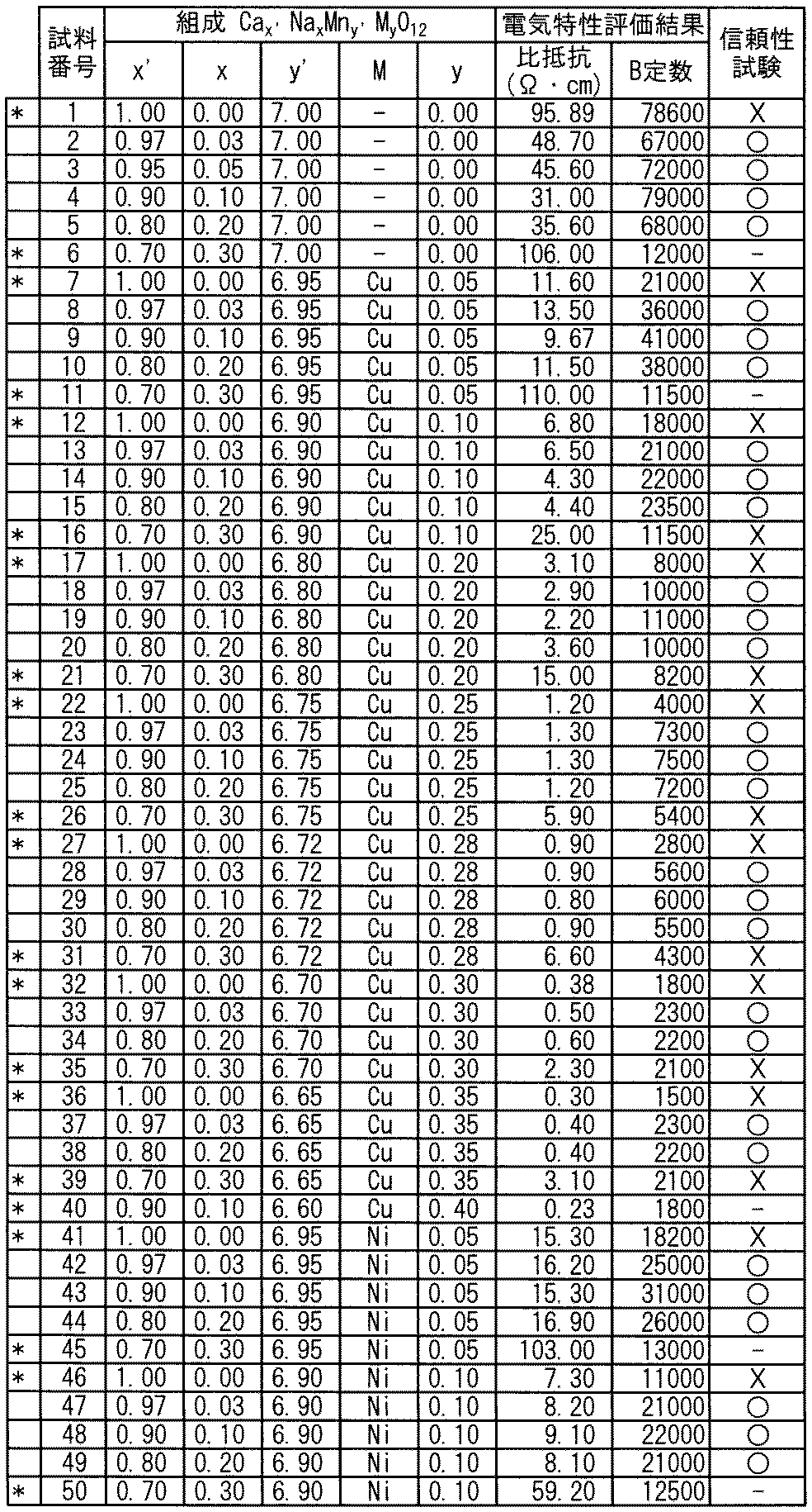
- sample preparation In order to evaluate electrical characteristics and reliability, a sample of a ceramic material was prepared by the following method. 99.9% or more of manganese oxide (Mn 3 O 4 ), calcium carbonate (CaCO 3 ), copper oxide (CuO), sodium carbonate (Na 2 CO 3 ), and nickel oxide (NiO) were used as raw materials. These raw materials are weighed so as to have the compositions shown in Tables 1 to 3 after firing, placed in a 500 ml pot container together with partially stabilized zirconium oxide (PSZ) balls having a diameter of 2 mm, pure water, and a dispersant, and pulverized and mixed for 16 hours. Went.
- PSZ partially stabilized zirconium oxide
- the slurry thus obtained was dried, granulated, and calcined at 900 ° C. for 4 hours in the air.
- An organic solvent and a dispersant are added to the calcined powder obtained in this manner, and the mixture is subjected to a pulverization and mixing treatment for 16 hours as a slurry using PSZ balls, and a plasticizer and an organic binder are added thereto and further mixed for 6 hours.
- a sheet forming slurry was prepared.
- the slurry thus prepared it was molded by a doctor blade method into a green sheet, cut into a strip shape, laminated and pressure-bonded, and a block (green body) was produced.
- the block is cut so as to have a size of about 5 mm ⁇ 5 mm ⁇ 0.8 mm, and is subjected to a binder removal treatment by heating at 450 ° C. in the atmosphere, and subsequently 950 to 980 in the atmosphere. Baked at 4 ° C. for 4 hours. An Ag paste was applied to the opposing main surfaces of the sintered body thus obtained and baked at 750 ° C. for 10 minutes to form an electrode. As described above, a sample provided with a pair of electrodes for electrical evaluation was obtained.
- the sample of sample number 1 (CaMn 7 O 12 ) has a room temperature specific resistance higher than 100 ⁇ ⁇ cm, and transitions from an insulator to a metal state around 180 ° C., showing a steep resistance change.
- the sample No. 4 within the scope of the present invention (the Ca site partially substituted with Na) is compared with the sample No. 1 sample.
- the steepness of the resistance change (B constant) is almost as high as that of sample No. 4, but the room temperature specific resistance is low and is 50 ⁇ ⁇ cm or less. In other words, it is understood that Sample No. 4 has a low room temperature specific resistance and realizes a steep resistance change (high B constant).
- the transition temperature can be shifted at a low temperature by adding Cu.
- the B constant tends to be smaller than in the case where Cu is not added.
- the effect of improving the B constant can be obtained by co-adding Na and Cu and adjusting the amount of these added.
- the Na amount x is 0.03 or more and less than 0.3 (particularly 0.2 or less)
- the Cu amount y is 0.35 or less (particularly 0.3 or less).
- the room temperature specific resistance is low and a steep resistance change (high B constant) is realized.
- the comparative samples of sample numbers 1 and 7 have a resistance change rate of more than 10% before and after the test, and the reliability is low. On the other hand, the resistance change rate was suppressed to 10% or less in the sample to which Na was added.
- the rapid resistance change seen in the CaMn 7 O 12 system is derived from the formation and collapse of the charge alignment state of Mn 3+ -Mn 4+. When the charge alignment state is inhibited, the rapid resistance change deteriorates (the B constant is low). Can be considered).
- the divalent Ca site with monovalent Na instead of the Mn site which greatly affects the charge alignment, holes can be injected without causing disturbance in the charge alignment of Mn. Thus, it is presumed that the specific resistance at room temperature was lowered and a high B constant could be maintained.
- the increase in room temperature resistance that occurs in the heat cycle may be affected by the generation of oxygen vacancies, and unstable oxygen is lost during the heat cycle test, resulting in a change in the amount of oxygen vacancies. Conceivable. In fact, the resistance tends to increase due to the heat cycle, and it is presumed that the oxygen deficiency is formed and the hole amount is decreased. On the other hand, by generating holes as in the present invention, even if the oxygen deficiency changes in the heat cycle, it is presumed that the charge was compensated and was not recognized as a significant resistance change. .
- the ceramic material of the present invention can be used as a material constituting the inrush current suppressing thermistor element, but is not limited to such an application.
Landscapes
- Engineering & Computer Science (AREA)
- Chemical & Material Sciences (AREA)
- Ceramic Engineering (AREA)
- Microelectronics & Electronic Packaging (AREA)
- Manufacturing & Machinery (AREA)
- Physics & Mathematics (AREA)
- Materials Engineering (AREA)
- Structural Engineering (AREA)
- Organic Chemistry (AREA)
- Electromagnetism (AREA)
- Inorganic Chemistry (AREA)
- Thermal Sciences (AREA)
- Thermistors And Varistors (AREA)
- Compositions Of Oxide Ceramics (AREA)
Abstract
Description
(1)R1がNdからなり、R2がSm、EuおよびGdのうちの少なくとも1種からなるとき、xが0.05≦x≦1.0であり、
(2)R1がNdからなり、R2がTb、Dy、Ho、ErおよびYのうちの少なくとも1種からなるとき、xが0.05≦x≦0.8であり、
(3)R1がSm、EuおよびGdのうちの少なくとも1種からなり、R2がTb、Dy、HoおよびYのうちの少なくとも1種からなるとき、xが0≦x≦0.4であり、
(4)R1がSm、EuおよびGdのうちの少なくとも1種からなり、R2がSm、EuおよびGdのうちのR1として選ばれなかった残りの少なくとも1種からなるとき、xが0≦x≦1.0である
ことを特徴とするセラミック材料が提案されている(特許文献1)。
Cax’NaxMny’MyO12
(式中、MはNiおよびCuの少なくとも一方を表し、
x’、x、y’およびyは、x’+x=X、およびy’+y=Yとして、以下の式(a)、(b)および(c)のいずれか:



で表される組成を有する、セラミック材料が提供される。
Ca含有モル部をx’、Na含有モル部をx、Mn含有モル部をy’、およびM含有モル部をyとし、x’+x=X、およびy’+y=Yとして、以下の式(a)、(b)および(c)のいずれか:



素子本体が本発明の上記いずれかのセラミック材料から構成される、抵抗素子が提供される。
Cax’NaxMny’MyO12
(式中、MはNiおよびCuの少なくとも一方を表し、
x’、xおよび、y’yは、x’+x=X、およびy’+y=Yとして、以下の式(a)、(b)および(c)のいずれか:



で表される組成を有する。
Ca含有モル部をx’、Na含有モル部をx、Mn含有モル部をy’、およびM含有モル部をyとし、x’+x=X、およびy’+y=Yとして、上記の式(a)、(b)および(c)のいずれかを満たすものであってもよい。
B定数=ln(R1/R2)/(1/T1-1/T2) ・・・(1)
式中、R1およびR2は、それぞれT1およびT2の温度(K)における抵抗値(Ω)を表す。
本実験例は、X=1.0およびY=7.0、よって、X/Y=1.0/7.0である場合、換言すれば、Ca1-xNaxMn7-yMyO12で表される組成(化学量論組成、言わば理想的な組成)を有するセラミック材料に関する。
電気的特性および信頼性を評価するため、セラミック材料の試料を下記の方法で作製した。
原料としてそれぞれ99.9%以上の酸化マンガン(Mn3O4)、炭酸カルシウム(CaCO3)、酸化銅(CuO)、炭酸ナトリウム(Na2CO3)、酸化ニッケル(NiO)を用いた。これら原料を焼成後に表1~3の組成になるように秤量し、500mlのポット容器に直径2mmの部分安定化酸化ジルコニウム(PSZ)ボール、純水、分散剤と一緒に入れ、16時間粉砕混合を行った。これにより得られたスラリーを乾燥させ、造粒して、大気中にて900℃で4時間仮焼した。これにより得られた仮焼粉に有機溶剤および分散剤を添加し、PSZボールを用いてスラリーとして16時間の粉砕混合処理に付し、これに可塑剤および有機バインダーを添加して更に6時間混合して、シート成形用スラリーを調製した。これにより調製したスラリーを用いて、ドクターブレード法により成形してグリーンシートとし、短冊状にカットし、これを積層して圧着し、ブロック(グリーンボディ)を作製した。その後、焼成後に約5mm×5mm×0.8mm程度のサイズになるようにブロックをカットし、大気中にて450℃で加熱することにより脱バインダー処理に付し、引き続き大気中にて950~980℃にて4時間焼成した。これにより得られた焼結体の相対向する主面にAgペーストを塗布し、750℃にて10分間の熱処理により焼き付けて電極を形成した。以上により、電気評価用に1対の電極を備える試料を得た。
上記のようにして作製した試料について、下記の通り電気特性を評価した。
抵抗測定器(ケースレー2430)と温度槽(Despatch製)とを使用して、4端子法で抵抗の温度依存性評価を行った。温度範囲は室温(28℃)~200℃とした。測定された抵抗値から比抵抗を算出し、また、5℃刻みで測定した抵抗値の温度依存性から、上述の式(1)に基づいてB定数を算出した。この実験例においては、室温(28℃)での比抵抗が50Ω・cm以下であり、かつ急激に抵抗変化が起きる温度領域でのB定数が2000以上の場合に、比抵抗が小さく、かつ抵抗変化の急峻性が高いと判断して、合格判定とした。室温(28℃)での比抵抗と、急激に抵抗変化が起きる温度領域でのB定数を表1~3に示す。
加えて、室温比抵抗とB定数が上記判断で合格判定となった試料と比較試料(試料番号1)においては、ヒートサイクル試験も行った。
この実験例においては、ヒートサイクル試験では-25℃~180℃の温度範囲で昇降温を1000回繰り返し、試験前後での抵抗変化率が10%以下の場合を合格判定とした。結果を表1~3に併せて示す。

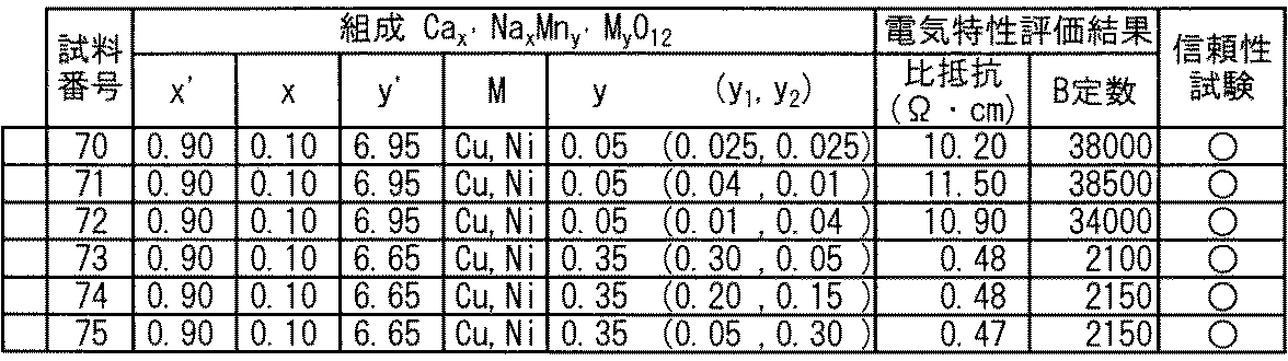
本実験例は、XおよびYが、X/Y=1.0/7.0を満たさない場合、換言すれば、セラミック材料の組成比率を、Ca1-xNaxMn7-yMyO12で表される理想的な組成から意図的にずらした場合に関するものであって、理想的な組成と比較して示すものである。


2 素子本体
3 電極
5 はんだ
6、7 リード線
Claims (5)
- 以下の式:
Cax’NaxMny’MyO12
(式中、MはNiおよびCuの少なくとも一方を表し、
x’、x、y’およびyは、x’+x=X、およびy’+y=Yとして、以下の式(a)、(b)および(c)のいずれか:


を満たす)
で表される組成を有する、セラミック材料。 - Ca、Na、MnおよびM(MはNiおよびCuの少なくとも一方を表す)の複合酸化物から構成されるセラミック材料であって、
Ca含有モル部をx’、Na含有モル部をx、Mn含有モル部をy’、およびM含有モル部をyとし、x’+x=X、およびy’+y=Yとして、以下の式(a)、(b)および(c)のいずれか:


を満たす、セラミック材料。
- 素子本体と、該素子本体の少なくとも一部を挟んで形成される少なくとも2つの電極とを備える、抵抗素子であって、
前記素子本体が請求項1または2に記載のセラミック材料から構成される、抵抗素子。 - 突入電流を抑制するためのサーミスタ素子として用いられる、請求項3に記載の抵抗素子。
- 前記素子本体は板状をなし、前記2つの電極は、互いに対向するように、板状の該素子本体の各主面上に形成される、請求項3または4に記載の抵抗素子。
Priority Applications (3)
| Application Number | Priority Date | Filing Date | Title |
|---|---|---|---|
| DE112016002459.2T DE112016002459B4 (de) | 2015-06-04 | 2016-06-03 | Widerstandselement |
| JP2017522274A JP6512289B2 (ja) | 2015-06-04 | 2016-06-03 | セラミック材料および抵抗素子 |
| US15/823,664 US10134512B2 (en) | 2015-06-04 | 2017-11-28 | Ceramic material and resistive element |
Applications Claiming Priority (2)
| Application Number | Priority Date | Filing Date | Title |
|---|---|---|---|
| JP2015114131 | 2015-06-04 | ||
| JP2015-114131 | 2015-06-04 |
Related Child Applications (1)
| Application Number | Title | Priority Date | Filing Date |
|---|---|---|---|
| US15/823,664 Continuation US10134512B2 (en) | 2015-06-04 | 2017-11-28 | Ceramic material and resistive element |
Publications (1)
| Publication Number | Publication Date |
|---|---|
| WO2016195065A1 true WO2016195065A1 (ja) | 2016-12-08 |
Family
ID=57441358
Family Applications (1)
| Application Number | Title | Priority Date | Filing Date |
|---|---|---|---|
| PCT/JP2016/066560 Ceased WO2016195065A1 (ja) | 2015-06-04 | 2016-06-03 | セラミック材料および抵抗素子 |
Country Status (4)
| Country | Link |
|---|---|
| US (1) | US10134512B2 (ja) |
| JP (1) | JP6512289B2 (ja) |
| DE (1) | DE112016002459B4 (ja) |
| WO (1) | WO2016195065A1 (ja) |
Citations (2)
| Publication number | Priority date | Publication date | Assignee | Title |
|---|---|---|---|---|
| JPH08198674A (ja) * | 1995-01-18 | 1996-08-06 | Murata Mfg Co Ltd | 負の抵抗温度特性を有する半導体セラミックとそれを用いた半導体セラミック部品 |
| JP2005051103A (ja) * | 2003-07-30 | 2005-02-24 | Japan Science & Technology Agency | n型熱電特性を有する複合酸化物 |
Family Cites Families (5)
| Publication number | Priority date | Publication date | Assignee | Title |
|---|---|---|---|---|
| JP3286906B2 (ja) * | 1997-10-21 | 2002-05-27 | 株式会社村田製作所 | 負の抵抗温度特性を有する半導体セラミック素子 |
| DE602007004871D1 (de) * | 2007-12-21 | 2010-04-01 | Vishay Resistors Belgium Bvba | Stabiler Thermistor |
| CN102224119B (zh) * | 2008-12-12 | 2014-03-26 | 株式会社村田制作所 | 半导体陶瓷以及正温度系数热敏电阻 |
| WO2012056797A1 (ja) | 2010-10-27 | 2012-05-03 | 株式会社村田製作所 | 半導体セラミックおよび抵抗素子 |
| JP2017143090A (ja) * | 2016-02-08 | 2017-08-17 | Tdk株式会社 | 半導体磁器組成物およびptcサーミスタ |
-
2016
- 2016-06-03 WO PCT/JP2016/066560 patent/WO2016195065A1/ja not_active Ceased
- 2016-06-03 DE DE112016002459.2T patent/DE112016002459B4/de active Active
- 2016-06-03 JP JP2017522274A patent/JP6512289B2/ja active Active
-
2017
- 2017-11-28 US US15/823,664 patent/US10134512B2/en active Active
Patent Citations (2)
| Publication number | Priority date | Publication date | Assignee | Title |
|---|---|---|---|---|
| JPH08198674A (ja) * | 1995-01-18 | 1996-08-06 | Murata Mfg Co Ltd | 負の抵抗温度特性を有する半導体セラミックとそれを用いた半導体セラミック部品 |
| JP2005051103A (ja) * | 2003-07-30 | 2005-02-24 | Japan Science & Technology Agency | n型熱電特性を有する複合酸化物 |
Also Published As
| Publication number | Publication date |
|---|---|
| DE112016002459T5 (de) | 2018-02-22 |
| DE112016002459B4 (de) | 2024-09-12 |
| JP6512289B2 (ja) | 2019-05-15 |
| US20180082770A1 (en) | 2018-03-22 |
| JPWO2016195065A1 (ja) | 2018-03-29 |
| US10134512B2 (en) | 2018-11-20 |
Similar Documents
| Publication | Publication Date | Title |
|---|---|---|
| US9472326B2 (en) | Semiconductor ceramic composition and PTC thermistor | |
| KR101793895B1 (ko) | Ptc 서미스터 자기 조성물 및 ptc 서미스터 소자 | |
| KR20170016805A (ko) | 반도체 자기 조성물 및 ptc 서미스터 | |
| KR20120093834A (ko) | 반도체 자기 조성물 및 그 제조 방법, ptc 소자 및 발열 모듈 | |
| JP5418323B2 (ja) | 誘電体磁器組成物および電子部品 | |
| JP5445689B2 (ja) | 半導体セラミックおよび抵抗素子 | |
| JP5765611B2 (ja) | Ptc素子および発熱モジュール | |
| JP6648825B2 (ja) | セラミック材料および抵抗素子 | |
| CN101528632B (zh) | 半导体陶瓷组合物及其制备方法 | |
| JP6897792B2 (ja) | セラミック部材 | |
| JP5626204B2 (ja) | 半導体磁器組成物、発熱体及び発熱モジュール | |
| WO2016195065A1 (ja) | セラミック材料および抵抗素子 | |
| WO2013065441A1 (ja) | Ptcサーミスタおよびptcサーミスタの製造方法 | |
| JP5605432B2 (ja) | 半導体セラミックおよび抵抗素子 | |
| JP5263668B2 (ja) | 半導体磁器組成物 | |
| US11387021B2 (en) | Ceramic member and electronic device | |
| JP2012046372A (ja) | Ptc素子および発熱モジュール | |
| JP3823876B2 (ja) | 電圧依存性非直線抵抗体 | |
| JP5737634B2 (ja) | 半導体磁器組成物の製造方法 |
Legal Events
| Date | Code | Title | Description |
|---|---|---|---|
| 121 | Ep: the epo has been informed by wipo that ep was designated in this application |
Ref document number: 16803496 Country of ref document: EP Kind code of ref document: A1 |
|
| ENP | Entry into the national phase |
Ref document number: 2017522274 Country of ref document: JP Kind code of ref document: A |
|
| WWE | Wipo information: entry into national phase |
Ref document number: 112016002459 Country of ref document: DE |
|
| 122 | Ep: pct application non-entry in european phase |
Ref document number: 16803496 Country of ref document: EP Kind code of ref document: A1 |