WO2016190224A1 - Blackening plating solution and conductive substrate - Google Patents
Blackening plating solution and conductive substrate Download PDFInfo
- Publication number
- WO2016190224A1 WO2016190224A1 PCT/JP2016/064936 JP2016064936W WO2016190224A1 WO 2016190224 A1 WO2016190224 A1 WO 2016190224A1 JP 2016064936 W JP2016064936 W JP 2016064936W WO 2016190224 A1 WO2016190224 A1 WO 2016190224A1
- Authority
- WO
- WIPO (PCT)
- Prior art keywords
- layer
- blackening
- metal
- plating solution
- conductive substrate
- Prior art date
Links
Images


Classifications
-
- C—CHEMISTRY; METALLURGY
- C25—ELECTROLYTIC OR ELECTROPHORETIC PROCESSES; APPARATUS THEREFOR
- C25D—PROCESSES FOR THE ELECTROLYTIC OR ELECTROPHORETIC PRODUCTION OF COATINGS; ELECTROFORMING; APPARATUS THEREFOR
- C25D7/00—Electroplating characterised by the article coated
-
- C—CHEMISTRY; METALLURGY
- C25—ELECTROLYTIC OR ELECTROPHORETIC PROCESSES; APPARATUS THEREFOR
- C25D—PROCESSES FOR THE ELECTROLYTIC OR ELECTROPHORETIC PRODUCTION OF COATINGS; ELECTROFORMING; APPARATUS THEREFOR
- C25D3/00—Electroplating: Baths therefor
- C25D3/02—Electroplating: Baths therefor from solutions
- C25D3/56—Electroplating: Baths therefor from solutions of alloys
-
- H—ELECTRICITY
- H01—ELECTRIC ELEMENTS
- H01B—CABLES; CONDUCTORS; INSULATORS; SELECTION OF MATERIALS FOR THEIR CONDUCTIVE, INSULATING OR DIELECTRIC PROPERTIES
- H01B5/00—Non-insulated conductors or conductive bodies characterised by their form
- H01B5/14—Non-insulated conductors or conductive bodies characterised by their form comprising conductive layers or films on insulating-supports
Definitions
- the present invention relates to a blackening plating solution and a conductive substrate.
- the capacitive touch panel converts information on the position of the adjacent object on the panel surface into an electrical signal by detecting a change in capacitance caused by the object in proximity to the panel surface. Since the conductive substrate used in the capacitive touch panel is disposed on the surface of the display, the material of the conductive layer of the conductive substrate is required to have a low reflectance and be hard to be recognized.
- a material of the conductive layer used in the capacitive touch panel a material having a low reflectance and which is hard to be recognized is used, and a wiring is formed on a transparent substrate or a transparent film.
- Patent Document 1 discloses a transparent conductive film including a polymer film and a transparent conductive film comprising a metal oxide provided thereon by a vapor deposition method, as a transparent conductive film comprising a metal oxide
- ITO indium oxide-tin oxide
- the screen size of a display provided with a touch panel has been increased, and correspondingly, the area of a conductive substrate such as a transparent conductive film for a touch panel is also required to be increased.
- ITO has a high electric resistance value, there is a problem that it can not cope with the increase in the area of the conductive substrate.
- the reflection of light on the surface of the conductive layer using a metal such as copper has not been sufficiently suppressed.
- an object of the present invention is to provide a blackening plating solution for forming a blackening layer capable of sufficiently suppressing the reflection of light on the surface of a metal layer.
- a blackening plating solution containing nickel sulfate, zinc sulfate and amidosulfuric acid and having a pH of 4.0 or more and 6.5 or less.
- a blackening plating solution for forming a blackening layer capable of sufficiently suppressing the reflection of light on the surface of a metal layer.
- FIG. 4 is a cross-sectional view taken along line AA ′ of FIG. 3;
- FIG. 4 is a cross-sectional view taken along line AA ′ of FIG. 3;
- the blackening plating solution of the present embodiment can contain nickel sulfate, zinc sulfate and amidosulfuric acid, and can have a pH of 4.0 or more and 6.5 or less.
- the inventors of the present invention conducted intensive studies on a method of forming a blackened layer capable of sufficiently suppressing the reflection of light on the surface of the metal layer with high productivity.
- the productivity was low. Therefore, in order to form the blackened layer with high productivity, the inventors of the present invention studied to form the blackened layer using a wet method. Therefore, a blackening plating solution suitable for forming a blackening layer was examined.
- the blackening plating solution is preferably a plating solution capable of forming a layer containing nickel and zinc.
- the blackening plating solution of the present embodiment can contain nickel sulfate and zinc sulfate. Furthermore, by containing the amidosulfuric acid which functions as a complexing agent, it can suppress that a color nonuniformity arises in the formed blackening layer.
- the pH of the blackening plating solution is less than 4.0, the formed blackening layer may not have a color capable of sufficiently suppressing the reflection of light, so the pH is preferably 4.0 or more.
- the pH of the blackening plating solution exceeds 6.5, some components of the components of the blackening plating solution may precipitate, etc., and when the blackening plating solution is used to form a blackening layer, Color unevenness may occur in the blackened layer. Therefore, the pH of the blackening plating solution is preferably 6.5 or less.
- the agent used to adjust the pH of the blackening plating solution is not particularly limited, but it is preferable to use an alkali containing no metal component so as not to affect the blackening layer to be formed. For this reason, for example, it is preferable that pH is adjusted with ammonia water. That is, the blackening plating solution can contain ammonia (ammonia water) as a pH adjuster.
- the blackening plating solution of the present embodiment can contain nickel sulfate, zinc sulfate, and amidosulfuric acid, but the content of each component is not particularly limited, and the formation is performed. It can be selected arbitrarily according to the degree of suppression of the reflectance required for the blackening layer to be used.
- nickel sulfate is considered to exist as nickel sulfate hexahydrate in the blackening plating solution, but the concentration of nickel sulfate hexahydrate in the blackening plating solution is preferably 30 g / L or more. This is because by setting the concentration of nickel sulfate hexahydrate to 30 g / L or more, sufficient nickel can be supplied to the blackened layer to be formed, and generation of color unevenness and the like in the blackened layer can be suppressed. .
- the upper limit of the concentration of nickel sulfate hexahydrate in the blackening plating solution is not particularly limited, and can be added, for example, so as to be equal to or less than the saturation concentration of nickel sulfate hexahydrate.
- the content is preferably 100 g / L or less.
- zinc sulfate is considered to exist as zinc sulfate heptahydrate in the blackening plating solution, but the concentration of zinc sulfate heptahydrate in the blackening plating solution is 1.0 g / L or more and 7.5 g / L or more It is preferable that it is the following. This is more suitable for suppressing the reflection of light formed on the surface of the metal layer, in particular, by setting the concentration of zinc sulfate heptahydrate in the blackening plating solution to 1.0 g / L or more. This is because the light reflectance of the conductive substrate can be particularly suppressed. If the concentration of zinc sulfate heptahydrate is higher than 7.5 g / L, color unevenness may occur in the blackened layer to be formed, and therefore it is preferably 7.5 g / L or less.
- the ratio of the content (content weight) of zinc as the metal component to the total content (content weight) of nickel and zinc as the metal component contained in the blackening plating solution is 2% by weight or more and 20% by weight or less Is preferred.
- the blackening layer By simultaneously containing nickel and zinc, the blackening layer can be made a color suitable for suppressing light reflection on the surface of the metal layer. And, when the ratio of zinc as the metal component to the total weight of nickel and zinc as the metal component contained in the blackening plating solution is 2% by weight or more, the light reflection on the surface of the metal layer is suppressed. This is because the color can be made particularly suitable for the above, and the reflectance of the conductive substrate can be suppressed.
- the ratio of zinc as the metal component to the total weight of nickel and zinc as the metal component contained in the blackening plating solution is preferably 20% by weight or less.
- the concentration of amidosulfuric acid in the blackening plating solution is not particularly limited, but is preferably 10 g / L or more and 30 g / L or less, for example.
- the blackening plating solution of the present embodiment may contain any component other than nickel sulfate, zinc sulfate and amidosulfuric acid.
- a molybdenum (Mo) compound and / or a tin (Sn) compound can be added as an additive.
- the blackening plating solution of the present embodiment described above can be suitably used when forming a blackening layer capable of sufficiently suppressing the reflection of light on the surface of the metal layer of the conductive substrate.
- the blackening layer can be formed by a wet method such as electrolytic plating, so that the blackening layer is compared to the blackening layer conventionally formed by dry method.
- the blackened layer can be formed with good productivity.
- the conductive substrate of the present embodiment includes a transparent substrate, a metal layer formed on at least one surface of the transparent substrate, and a blackening layer formed using a blackening plating solution on the metal layer. You can have
- the conductive substrate in the present embodiment means a substrate having a metal layer and a blackening layer on the surface of a transparent base before patterning a metal layer etc., and a substrate having a metal layer etc. patterned. And a wiring board.
- the transparent substrate is not particularly limited, and a transparent substrate such as a resin substrate (resin film) which transmits visible light or a glass substrate can be preferably used.
- a transparent substrate such as a resin substrate (resin film) which transmits visible light or a glass substrate can be preferably used.
- resins such as polyamide resin, polyethylene terephthalate resin, polyethylene naphthalate resin, cycloolefin resin, polyimide resin, and polycarbonate resin can be preferably used.
- polyamide, PET (polyethylene terephthalate), COP (cycloolefin polymer), PEN (polyethylene naphthalate), polyimide, polycarbonate and the like can be more preferably used as the material of the resin substrate that transmits visible light.
- the thickness of the transparent substrate is not particularly limited, and can be arbitrarily selected according to the strength, the capacitance, the light transmittance, etc. required for the conductive substrate.
- the thickness of the transparent substrate can be, for example, 10 ⁇ m or more and 200 ⁇ m or less.
- the thickness of the transparent substrate is preferably 20 ⁇ m or more and 120 ⁇ m or less, and more preferably 20 ⁇ m or more and 100 ⁇ m or less.
- the thickness of the transparent substrate is preferably 20 ⁇ m to 50 ⁇ m.
- the total light transmittance of the transparent substrate is preferably high.
- the total light transmittance is preferably 30% or more, more preferably 60% or more.
- the visibility of the display can be sufficiently ensured, for example, when used for a touch panel application.
- the total light transmittance of the transparent substrate can be evaluated by the method defined in JIS K 7361-1.
- the material which comprises a metal layer is not specifically limited, although the material which has the electrical conductivity according to the application can be selected,
- the material which comprises a metal layer is Cu, Ni, Mo, Ta, Ti, V, Cr
- it is a copper alloy with at least one or more metals selected from Fe, Mn, Co, W, or a material containing copper.
- the metal layer can also be a copper layer composed of copper.
- the method of forming the metal layer on the transparent substrate is not particularly limited, but in order not to reduce the light transmittance, it is preferable not to dispose an adhesive between the transparent substrate and the metal layer. That is, the metal layer is preferably formed directly on at least one surface of the transparent substrate. When the adhesion layer is disposed between the transparent substrate and the metal layer as described later, the metal layer is preferably formed directly on the upper surface of the adhesion layer.
- the metal layer preferably has a metal thin film layer.
- the metal layer may have a metal thin film layer and a metal plating layer.
- a metal thin film layer can be formed on a transparent substrate by a dry plating method, and the metal thin film layer can be used as a metal layer.
- the metal layer can be formed directly on the transparent substrate without the use of an adhesive.
- a dry plating method for example, a sputtering method, a vapor deposition method, an ion plating method and the like can be preferably used.
- a metal thin film layer and a metal plating layer are formed by forming a metal plating layer by the electroplating method which is 1 type of the wet plating method by using a metal thin film layer as a feed layer. It can also be made to have a metal layer. Since the metal layer includes the metal thin film layer and the metal plating layer, the metal layer can be formed directly on the transparent substrate without an adhesive.
- the thickness of the metal layer is not particularly limited, and when the metal layer is used as a wire, it can be arbitrarily selected according to the magnitude of the current supplied to the wire, the wire width, and the like.
- the thickness of the metal layer is preferably 5 ⁇ m or less, more preferably 3 ⁇ m or less.
- the thickness of the metal layer is preferably 50 nm or more, more preferably 60 nm or more, and 150 nm It is more preferable that it is more than.
- a metal layer has a metal thin film layer and a metal plating layer as mentioned above, it is preferable that the sum total of the thickness of a metal thin film layer and the thickness of a metal plating layer is the said range.
- the thickness of the metal thin film layer is not particularly limited in any case where the metal layer is constituted of a metal thin film layer or in the case of having a metal thin film layer and a metal plating layer, for example, 50 nm or more and 500 nm It is preferable to set it as the following.
- the metal layer can be used as a wiring by patterning, for example, a desired wiring pattern as described later. And since the metal layer can lower the electric resistance value than ITO conventionally used as a transparent conductive film, the electric resistance value of the conductive substrate can be reduced by providing the metal layer.
- the blackening layer can be formed using the blackening plating solution described above. Therefore, for example, after forming the metal layer, it can be formed on the upper surface of the metal layer by a wet method such as electrolytic plating.
- the blackening layer can be a layer containing nickel and zinc, more specifically, a wet blackening layer.
- the thickness of the blackening layer is not particularly limited, but is preferably, for example, 30 nm or more, and more preferably 50 nm or more. This is because the reflection of light on the surface of the metal layer can be particularly suppressed by setting the thickness of the blackening layer to 30 nm or more.
- the upper limit of the thickness of the blackening layer is not particularly limited, but even if it is thicker than necessary, the time required for film formation and the time required for etching when forming a wiring become longer, and the cost rises Will lead to Therefore, the thickness of the blackening layer is preferably 120 nm or less, and more preferably 90 nm or less.
- the conductive substrate can be provided with any layer.
- an adhesive layer can be provided.
- the metal layer can be formed on the transparent substrate, but when the metal layer is formed directly on the transparent substrate, the adhesion between the transparent substrate and the metal layer may not be sufficient. . For this reason, when a metal layer is directly formed on the upper surface of the transparent substrate, the metal layer may peel off from the transparent substrate during the manufacturing process or during use.
- an adhesion layer in order to improve the adhesiveness of a transparent base material and a metal layer, an adhesion layer can be arranged on a transparent base material.
- the adhesion layer between the transparent base and the metal layer By arranging the adhesion layer between the transparent base and the metal layer, the adhesion between the transparent base and the metal layer can be enhanced, and peeling of the metal layer from the transparent base can be suppressed.
- the adhesion layer can also function as a blackening layer. For this reason, it becomes possible to suppress reflection of light of the metal layer by light from the lower surface side of the metal layer, that is, the transparent substrate side.
- the material constituting the adhesion layer is not particularly limited, and the adhesion between the transparent substrate and the metal layer, the required degree of suppression of light reflection on the surface of the metal layer, and the use of a conductive substrate It can be arbitrarily selected according to the degree of stability to the environment (eg, humidity, temperature) to be used.
- the adhesion layer preferably contains, for example, at least one metal selected from Ni, Zn, Mo, Ta, Ti, V, Cr, Fe, Co, W, Cu, Sn, and Mn.
- the adhesion layer can further contain one or more elements selected from carbon, oxygen, hydrogen and nitrogen.
- the adhesion layer can include a metal alloy containing at least two or more metals selected from Ni, Zn, Mo, Ta, Ti, V, Cr, Fe, Co, W, Cu, Sn, and Mn. Also in this case, the adhesion layer can further contain one or more elements selected from carbon, oxygen, hydrogen, and nitrogen.
- a metal alloy containing at least two or more metals selected from Ni, Zn, Mo, Ta, Ti, V, Cr, Fe, Co, W, Cu, Sn, and Mn a Cu-Ti-Fe alloy is used.
- Cu-Ni-Fe alloy, Ni-Cu alloy, Ni-Zn alloy, Ni-Ti alloy, Ni-W alloy, Ni-Cr alloy, Ni-Cu-Cr alloy can be preferably used.
- the film-forming method of the adhesion layer is not particularly limited, it is preferable to form a film by dry plating.
- a dry plating method for example, a sputtering method, an ion plating method, a vapor deposition method and the like can be preferably used.
- the adhesion layer is formed by a dry method, it is more preferable to use a sputtering method because control of the film thickness is easy.
- one or more elements selected from carbon, oxygen, hydrogen and nitrogen can be added to the adhesion layer, and in this case, reactive sputtering can be more preferably used.
- the atmosphere for forming the adhesion layer is at least one element selected from carbon, oxygen, hydrogen and nitrogen
- the atmosphere for forming the adhesion layer is at least one element selected from carbon, oxygen, hydrogen and nitrogen
- a gas containing For example, carbon monoxide gas and / or carbon dioxide gas when carbon is added to the adhesion layer, oxygen gas when oxygen is added, hydrogen gas and / or water when hydrogen is added, When nitrogen is added, nitrogen gas can be added to the atmosphere at the time of performing dry plating.
- a gas containing one or more elements selected from carbon, oxygen, hydrogen, and nitrogen is preferably added to an inert gas and used as an atmosphere gas in dry plating.
- the inert gas is not particularly limited but, for example, argon can be preferably used.
- the adhesion between the transparent substrate and the adhesion layer can be enhanced by forming the adhesion layer by dry plating as described above. And since the adhesion layer can contain, for example, a metal as a main component, the adhesion to the metal layer is also high. For this reason, peeling of a metal layer can be suppressed by arrange
- the thickness of the adhesion layer is not particularly limited, but is preferably 3 nm to 50 nm, more preferably 3 nm to 35 nm, and still more preferably 3 nm to 33 nm.
- the thickness of the adhesion layer is preferably 3 nm or more as described above.
- the upper limit of the thickness of the adhesion layer is not particularly limited, but even if it is thicker than necessary, the time required for film formation and the time required for etching when forming a wiring become longer, and the cost increases. It will incur. Therefore, as described above, the thickness of the adhesive layer is preferably 50 nm or less, more preferably 35 nm or less, and still more preferably 33 nm or less.
- the conductive substrate of the present embodiment can have a transparent substrate, a metal layer, and a blackening layer. Moreover, layers, such as an adhesion layer, can also be provided arbitrarily.
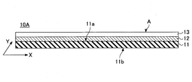
- FIGS. 1A and 1B show examples of cross-sectional views in a plane parallel to the stacking direction of the transparent base material, the metal layer, and the blackening layer of the conductive substrate of the present embodiment.
- the conductive substrate of the present embodiment can have, for example, a structure in which a metal layer and a blackening layer are laminated in this order from the transparent substrate side on at least one surface of the transparent substrate.
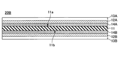
- the metal layer 12 and the blackening layer 13 may be sequentially laminated one by one on the one surface 11a side of the transparent substrate 11 it can. Further, as in the case of the conductive substrate 10B shown in FIG. 1B, the metal layers 12A and 12B and the black are respectively provided on the side of the surface 11a of the transparent substrate 11 and the other side (the other surface) 11b. And the barrier layers 13A and 13B can be stacked one by one in that order.
- an adhesion layer may be provided as an arbitrary layer.
- an adhesion layer, a metal layer, and a blackening layer can be formed in this order on at least one surface of the transparent substrate from the transparent substrate side.
- the adhesion layer 14, the metal layer 12, and the blackening layer 13 are laminated in this order on one surface 11a side of the transparent substrate 11. be able to.
- the adhesion layer, the metal layer, and the blackening layer may be laminated on both surfaces of the transparent substrate 11.
- the adhesion layers 14A and 14B and the metal layers 12A and 12B are formed on one surface 11a side and the other surface 11b side of the transparent substrate 11, respectively.
- the blackening layers 13A and 13B can be stacked in that order.
- FIG. 1B and FIG. 2B when metal layers, blackening layers, etc. are laminated on both sides of the transparent substrate, the layers laminated on the upper and lower sides of the transparent substrate 11 with the transparent substrate 11 as the symmetry plane become symmetrical.
- positioned as shown was shown, it is not limited to the form which concerns.
- the configuration on one surface 11a side of the transparent substrate 11 is the same as the configuration of FIG. 1B, in which the metal layer 12A and the blackening layer 13A are laminated in that order without providing the adhesion layer 14A.
- the layers stacked on the upper and lower sides of the transparent substrate 11 may be asymmetric.
- the metal layer and the blackening layer on the transparent substrate, it is possible to suppress the reflection of light by the metal layer and to suppress the reflectance of the conductive substrate. Can.
- the degree of reflectance of the conductive substrate of the present embodiment is not particularly limited, but for example, in order to enhance the visibility of the display when used as a conductive substrate for a touch panel, one having a low reflectance Is good.
- the average reflectance of light with a wavelength of 400 nm or more and 700 nm or less is preferably 20% or less, and more preferably 19% or less.
- the measurement of reflectance can be performed by irradiating light to the blackened layer of the conductive substrate. Specifically, for example, when the metal layer 12 and the blackening layer 13 are laminated in this order on one surface 11a side of the transparent substrate 11 as shown in FIG. 1A, the blackening layer 13 is irradiated so as to irradiate light.
- the surface A of the light can be irradiated with light and measured.
- light having a wavelength of 400 nm or more and 700 nm or less is irradiated to the blackened layer 13 of the conductive substrate at an interval of 1 nm as described above, for example, and the average value of the measured values is the reflectance of the conductive substrate be able to.
- the conductive substrate of the present embodiment can be preferably used as a conductive substrate for a touch panel.
- the conductive substrate can be configured to have mesh-like wiring.
- the conductive substrate provided with the mesh-like wiring can be obtained by etching the metal layer and the blackening layer of the conductive substrate of the present embodiment described above.
- FIG. 3 is a view of the conductive substrate 30 provided with the mesh-like wiring as viewed from the upper surface side in the stacking direction of the metal layer etc., and the transparent base material and the metal layer are patterned so that the wiring pattern can be easily understood. Layers other than the wirings 31A and 31B formed are omitted.
- the conductive substrate 30 shown in FIG. 3 has a transparent base 11, a plurality of wirings 31A parallel to the Y-axis direction in the drawing, and a wiring 31B parallel to the X-axis direction.
- the wirings 31A and 31B are formed by etching a metal layer, and a blackening layer (not shown) is formed on the upper surface or the lower surface of the wirings 31A and 31B.
- the blackening layer is etched to the same shape as the wirings 31A and 31B.
- the arrangement of the transparent substrate 11 and the wirings 31A and 31B is not particularly limited.
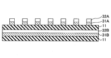
- positioning with the transparent base material 11 and wiring is shown to FIG. 4A and FIG. 4B.
- 4A and 4B correspond to cross-sectional views taken along the line AA 'of FIG.
- the wirings 31A and 31B may be disposed on the upper and lower surfaces of the transparent substrate 11, respectively.
- blackened layers 32A and 32B etched in the same shape as the wiring are arranged on the upper surface of the wiring 31A and the lower surface of the wiring 31B.
- wiring 31A, 31B is arrange
- an adhesion layer may be provided in addition to the metal layer and the blackening layer. For this reason, in any case of FIG. 4A and FIG. 4B, for example, an adhesion layer can be provided between the wiring 31A and / or the wiring 31B and the transparent base material 11. When the adhesion layer is provided, the adhesion layer is also preferably etched to the same shape as the wirings 31A and 31B.
- the conductive substrate having the mesh-like wiring shown in FIGS. 3 and 4A is, for example, a conductive substrate provided with metal layers 12A and 12B and blackening layers 13A and 13B on both sides of the transparent substrate 11 as shown in FIG. 1B. Can be formed from a flexible substrate.
- the metal layer 12A and the blackening layer 13A on one side 11a of the transparent substrate 11 are parallel to the Y-axis direction in FIG. 1B.
- the etching is performed such that a plurality of linear patterns are arranged at predetermined intervals along the X-axis direction.
- the X-axis direction in FIG. 1B means a direction parallel to the width direction of each layer.
- the Y-axis direction in FIG. 1B means a direction perpendicular to the paper surface in FIG. 1B.
- a plurality of linear patterns parallel to the X-axis direction in FIG. 1B are formed along the Y-axis direction at predetermined intervals, with the metal layer 12B on the other surface 11b side of the transparent substrate 11 and the blackening layer 13B. Do the etching to be placed.
- the conductive substrate having the mesh-like wiring shown in FIG. 3 and FIG. 4A can be formed.
- the etching of both surfaces of the transparent base material 11 can also be performed simultaneously. That is, the etching of the metal layers 12A and 12B and the blackening layers 13A and 13B may be performed simultaneously.
- a conductive substrate having an adhesive layer patterned in the same shape as the wires 31A and 31B between the wires 31A and 31B and the transparent substrate 11 is the conductive substrate shown in FIG. 2B. It can produce by using and etching similarly.
- the conductive substrate having the mesh-like wiring shown in FIG. 3 can also be formed by using two conductive substrates shown in FIG. 1A or FIG. 2A.
- a case where two conductive substrates shown in FIG. 1A are formed will be described by way of example.
- a plurality of metal layers 12 and a plurality of blackening layers 13 are parallel to the X-axis direction.
- the etching is performed such that the linear patterns of are arranged at predetermined intervals along the Y-axis direction.
- a conductive substrate provided with a mesh-like wiring is obtained.
- the surface to be bonded when bonding the two conductive substrates is not particularly limited.
- the surface A in FIG. 1A in which the metal layer 12 and the like are laminated and the other surface 11b in FIG. 1A in which the metal layer 12 and the like are not laminated are bonded to obtain the structure shown in FIG. It can also be done.
- the other surfaces 11b in FIG. 1A where the metal layer 12 and the like of the transparent base material 11 are not laminated may be bonded to each other to have a cross section shown in FIG. 4A.
- the conductive substrate having the adhesion layer patterned in the same shape as the wires 31A and 31B between the wires 31A and 31B and the transparent base 11 is the conductive shown in FIG. 1A.
- the conductive substrate shown in FIG. 2A can be used instead of the conductive substrate.
- the width of the wires and the distance between the wires in the conductive substrate having the mesh-like wires shown in FIGS. 3, 4A and 4B are not particularly limited, and, for example, according to the amount of current flowing in the wires It can be selected.
- a wiring pattern The wiring which comprises can be made into arbitrary shapes.
- the shapes of the wires forming the mesh-like wiring pattern may be various shapes such as lines (zigzag straight lines) bent in a jagged manner so as not to generate moire (interference fringes) with the image of the display.
- the conductive substrate having mesh-like wiring composed of two layers of wiring can be preferably used, for example, as a conductive substrate for a projected capacitive touch panel.
- the blackening layer is laminated on the metal layer formed on at least one surface of the transparent substrate. And since a blackening layer is formed using the blackening plating solution as stated above, reflection of the light in the metal layer surface can fully be suppressed, and it can be set as the conductive substrate which suppressed the reflectance. Also, for example, when used for applications such as touch panels, the visibility of the display can be enhanced.
- the blackening layer can be formed by the wet method using the blackening plating solution described above, the conductive substrate can be produced with high productivity as compared with the case where the blackening layer is formed using the conventional dry method. It can be produced. (Method of manufacturing conductive substrate) Next, one configuration example of the method of manufacturing the conductive substrate of the present embodiment will be described.
- the method for producing a conductive substrate of the present embodiment can have the following steps.
- Blackening layer formation process which forms a blackening layer using a blackening plating solution on a metal layer.
- the blackening plating solution whose pH is 4.0 or more and 6.5 or less containing nickel sulfate, zinc sulfate, and amidosulfuric acid as stated above can be used.
- the above-mentioned conductive substrate can be suitably manufactured by the manufacturing method of the conductive substrate of this embodiment. For this reason, since it can be set as the same structure as the case of the above-mentioned conductive substrate except the point explained below, explanation is omitted in part.
- the transparent substrate to be subjected to the metal layer forming step can be prepared in advance.
- the kind of transparent substrate to be used is not particularly limited, but as described above, a transparent substrate such as a resin substrate (resin film) that transmits visible light, a glass substrate, etc. can be preferably used.
- the transparent substrate can be cut into any size in advance, if necessary.
- the metal layer preferably has a metal thin film layer as described above.
- the metal layer can also have a metal thin film layer and a metal plating layer.
- a metal layer formation process can have the process of forming a metal thin film layer, for example by the dry plating method.
- a dry plating method used at the process of forming a metal thin film layer For example, a vapor deposition method, sputtering method, or ion plating method etc. can be used.
- a vacuum evaporation method can be preferably used as an evaporation method.
- the dry plating method used in the step of forming the metal thin film layer it is more preferable to use the sputtering method because the control of the film thickness is particularly easy.
- a metal plating layer is demonstrated.
- the conditions in the step of forming the metal plating layer by the wet plating method that is, the conditions of the electroplating treatment are not particularly limited, and various conditions in the usual way may be adopted.
- a metal plating layer can be formed by supplying a base having a metal thin film layer formed in a plating tank containing a metal plating solution and controlling the current density and the conveyance speed of the base.
- the blackening layer can be formed using a blackening plating solution containing nickel sulfate, zinc sulfate and amidosulfuric acid as described above and having a pH of 4.0 or more and 6.5 or less.
- the blackened layer can be formed by a wet method. Specifically, for example, using a metal layer as a feed layer, a blackening layer can be formed on the metal layer by electrolytic plating in a plating tank containing the above-described blackening plating solution. By forming the blackening layer by electrolytic plating using the metal layer as the feeding layer as described above, the blackening layer can be formed on the entire surface of the metal layer opposite to the side facing the transparent base.
- an arbitrary step can be further performed in addition to the above-described steps.
- an adhesion layer formation process which forms an adhesion layer on the field which forms a metal layer of a transparent base material can be carried out.
- the metal layer formation step can be carried out after the adhesion layer formation step, and in the metal layer formation step, metal is formed on the base on which the adhesion layer is formed on the transparent substrate in this step.
- a thin film layer can be formed.
- the film formation method of the adhesion layer is not particularly limited, but it is preferable to form a film by a dry plating method.
- a dry plating method for example, a sputtering method, an ion plating method, a vapor deposition method and the like can be preferably used.
- the adhesion layer is formed by a dry method, it is more preferable to use a sputtering method because control of the film thickness is easy.
- one or more elements selected from carbon, oxygen, hydrogen and nitrogen can be added to the adhesion layer, and in this case, reactive sputtering can be more preferably used.
- the conductive substrate obtained by the method for producing a conductive substrate of the present embodiment can be used, for example, in various applications such as a touch panel. And when using for various uses, it is preferable that the metal layer contained in the conductive substrate of this embodiment, and a blackening layer are patterned. When the adhesion layer is provided, it is preferable that the adhesion layer is also patterned.
- the metal layer and the blackening layer, and optionally also the adhesion layer can be patterned, for example according to the desired wiring pattern, and the metal layer and the blackening layer, optionally also the adhesion layer, are patterned in the same shape It is preferable that the
- the manufacturing method of the conductive substrate of this embodiment can have a patterning step of patterning a metal layer and a blackening layer.
- the patterning step can be a step of patterning the adhesion layer, the metal layer, and the blackening layer.
- the specific procedure of the patterning step is not particularly limited, and can be performed by any procedure.
- a mask having a desired pattern is disposed on the surface A on the blackening layer 13.
- a mask placement step can be performed.
- an etching step may be performed in which the etchant is supplied to the surface A on the blackening layer 13, ie, the surface on which the mask is disposed.
- the etchant used in the etching step is not particularly limited, and can be arbitrarily selected according to the material constituting the layer to be etched.
- the etching solution can be changed layer by layer, or the metal layer and the blackening layer and, in some cases, the adhesion layer can be simultaneously etched with the same etching solution.
- the patterning process can be carried out to pattern the conductive substrate 10B in which the metal layers 12A and 12B and the blackening layers 13A and 13B are stacked on one surface 11a and the other surface 11b of the transparent substrate 11. .
- a mask disposing step of disposing a mask having a desired pattern on the surface A and the surface B on the blackening layers 13A and 13B can be performed.
- an etching step may be performed in which the etchant is supplied to the surface A and the surface B on the blackened layers 13A and 13B, that is, the surface on which the mask is disposed.
- the pattern to be formed in the etching step is not particularly limited, and may have an arbitrary shape.
- a pattern is formed so that the metal layer 12 and the blackening layer 13 include a plurality of straight lines or lines bent in zigzag (zigzag straight lines) as described above. Can.
- the metal layer 12A and the metal layer 12B can form a pattern so as to form a mesh-like wiring.
- the blackening layer 13A is preferably patterned to have the same shape as the metal layer 12A
- the blackening layer 13B is preferably patterned to have the same shape as the metal layer 12B.
- stacks two or more patterned conductive substrates can also be implemented.
- laminating for example, by laminating so that the patterns of the metal layers of the respective conductive substrates intersect, it is also possible to obtain a laminated conductive substrate provided with a mesh-like wiring.
- the method of fixing the laminated two or more conductive substrates is not particularly limited, for example, it can be fixed by an adhesive or the like.
- the conductive substrate obtained by the method for producing a conductive substrate of the present embodiment described above has a structure in which a blackening layer is laminated on a metal layer formed on at least one surface of a transparent substrate. . And since a blackening layer is formed using the blackening plating solution as stated above, reflection of the light in the metal layer surface can fully be suppressed, and it can be set as the conductive substrate which suppressed the reflectance. Also, for example, when used for applications such as touch panels, the visibility of the display can be enhanced.
- the blackening layer can be formed by the wet method using the blackening plating solution described above, the conductive substrate can be produced with high productivity as compared with the case where the blackening layer is formed using the conventional dry method. It can be produced.
- a conductive substrate having a structure shown in FIG. 1A was produced.
- the reflectance measurement is performed with light having a wavelength of 400 nm or more and 700 nm or less at an interval of 1 nm with an incident angle of 5 ° and a light receiving angle of 5 °
- the specular reflectance was measured by irradiation, and the average value was taken as the reflectance (average reflectance) of the conductive substrate.
- Evaluation of the appearance of the blackened layer The appearance of the formed blackened layer is evaluated visually, and it is judged to be good if it has a uniform color without color unevenness, and color unevenness occurs. Was judged to be bad.
- Judgment The reflectivity of the conductive substrate was 20% or less, and the conductive substrate was evaluated as excellent in the appearance evaluation of the blackened layer.
- Example preparation conditions In each of the following experimental examples, a conductive substrate was produced under the conditions described below, and evaluated by the above-described evaluation method.
- Experimental Example 1 In Experimental Example 1, six types of blackening plating solutions of Experimental Examples 1-1 to 1-6 in which the pH of the plating solution is different are prepared, and a conductive substrate is prepared using the blackening plating solution of each experimental example. It produced and evaluated.
- Experimental Examples 1-2 to 1-5 are Examples, and Experimental Examples 1-1 and 1-6 are Comparative Examples.
- (1) Blackening Plating Solution The blackening plating solution prepared in this experimental example will be described.
- the concentration of nickel sulfate hexahydrate is 40 g / L
- the concentration of zinc sulfate heptahydrate is 5 g / L
- the concentration of amidosulfuric acid is 11 g / L.
- Each component was mixed.
- ammonia water was further added to prepare the blackening plating solution of each experimental example so that the pH of each blackening plating solution of Experimental Example 1-1 to Experimental Example 1-6 was the value shown in Table 1. .
- Conductive substrate (metal layer forming process) A metal layer was formed on one side of a transparent substrate made of polyethylene terephthalate resin (PET) having a length of 100 m, a width of 500 mm, and a thickness of 100 ⁇ m.
- PET polyethylene terephthalate resin
- the total light transmittance of the transparent substrate made of polyethylene terephthalate resin used as the transparent substrate was evaluated by the method defined in JIS K 7361-1 and found to be 97%.
- a metal thin film layer forming step and a metal plating layer forming step were performed.
- a copper thin film layer was formed as a metal thin film layer on one surface of the transparent base material using the above-mentioned transparent base material as a base material.
- the metal thin film layer forming step first, the above-mentioned transparent substrate from which water was removed by heating in advance to 60 ° C. was placed in the chamber of the sputtering apparatus.
- Electric power was supplied to a copper target previously set at the cathode of the sputtering apparatus, and a copper thin film layer was formed to a thickness of 0.2 ⁇ m on one surface of the transparent substrate.
- a copper plating layer was formed as the metal plating layer.
- the copper plating layer was formed by electroplating so that the thickness of the copper plating layer was 0.3 ⁇ m.
- a copper layer having a thickness of 0.5 ⁇ m was formed as a metal layer.
- the substrate having a 0.5 ⁇ m thick copper layer formed on a transparent substrate prepared in the metal layer forming step was immersed in 20 g / L sulfuric acid for 30 seconds and washed, and the following blackening layer forming step was carried out .
- Blackening layer formation process In the blackening layer forming step, a blackening layer was formed on one surface of the metal layer by electrolytic plating using a blackening plating solution prepared in advance for each experimental example. In the blackening layer formation step, the electrolytic plating is performed under the conditions of a temperature of blackening plating solution of 40 ° C., a current density of 0.4 A / dm 2 , and a plating time of 50 seconds in any of the experimental examples. A layer was formed.
- the film thickness of the formed blackened layer was 70 nm.
- the blackening plating solution prepared in this experimental example was prepared by mixing nickel sulfate hexahydrate, zinc sulfate heptahydrate and amidosulfuric acid so as to have predetermined concentrations.
- Zinc sulfate heptahydrate is a metal component relative to the total content of nickel and zinc as a metal component when nickel sulfate hexahydrate is added to a concentration shown in Table 2 in each experimental example. It added so that the metal zinc rate which is a ratio of the content of zinc as it will be 10.0 weight%.
- Experimental Example 3 In Experimental Example 3, seven types of blackening plating solutions of Experimental Example 3-1 to Experimental Example 3-7, which have different concentrations of zinc sulfate heptahydrate in the blackening plating solution, are prepared, and A conductive substrate was produced using a blackening plating solution and evaluated. Experimental Examples 3-1 to 3-7 are all examples.
- (1) Blackening Plating Solution The blackening plating solution prepared in this experimental example will be described.
- the blackening plating solution prepared in this experimental example was prepared by mixing nickel sulfate hexahydrate, zinc sulfate heptahydrate and amidosulfuric acid so as to have predetermined concentrations.
- Amidosulfuric acid was added to a concentration of 11 g / L. Then, ammonia water was further added to adjust the pH of the blackening plating solution to 6 to prepare a blackening plating solution of each experimental example.
- Table 3 also shows the metal zinc ratio of the blackening plating solution prepared in each experimental example.
- Conductive Substrate A conductive substrate of each experimental example was produced in the same manner as in experimental example 1 except that the blackening plating solution of each experimental example was used in the blackening layer forming step.
Abstract
Provided is a blackening plating solution, which comprises nickel sulfate, zinc sulfate, and sulfamic acid and which has a pH of 4.0 to 6.5.
Description
本発明は、黒化めっき液、導電性基板に関する。
The present invention relates to a blackening plating solution and a conductive substrate.
静電容量式タッチパネルは、パネル表面に近接する物体により引き起こされる静電容量の変化を検出することにより、パネル表面上での近接する物体の位置の情報を電気信号に変換する。静電容量式タッチパネルに用いられる導電性基板は、ディスプレイの表面に設置されるため、導電性基板の導電層の材料には反射率が低く、視認されにくいことが要求されている。
The capacitive touch panel converts information on the position of the adjacent object on the panel surface into an electrical signal by detecting a change in capacitance caused by the object in proximity to the panel surface. Since the conductive substrate used in the capacitive touch panel is disposed on the surface of the display, the material of the conductive layer of the conductive substrate is required to have a low reflectance and be hard to be recognized.
そこで、静電容量式タッチパネルに用いられる導電層の材料としては、反射率が低く、視認されにくい材料が用いられ、透明基板または透明なフィルム上に配線が形成されている。
Therefore, as a material of the conductive layer used in the capacitive touch panel, a material having a low reflectance and which is hard to be recognized is used, and a wiring is formed on a transparent substrate or a transparent film.
例えば特許文献1には、高分子フィルムおよびその上に気相成膜法により設けられた金属酸化物からなる透明導電膜を含む透明導電性フィルムが開示され、金属酸化物からなる透明導電膜として酸化インジウム-酸化スズ(ITO)膜を用いることが開示されている。
For example, Patent Document 1 discloses a transparent conductive film including a polymer film and a transparent conductive film comprising a metal oxide provided thereon by a vapor deposition method, as a transparent conductive film comprising a metal oxide The use of indium oxide-tin oxide (ITO) films is disclosed.
ところで、近年タッチパネルを備えたディスプレイの大画面化が進んでおり、これに対応してタッチパネル用の透明導電性フィルム等の導電性基板についても大面積化が求められている。しかし、ITOは電気抵抗値が高いため、導電性基板の大面積化に対応できないという問題があった。
By the way, in recent years, the screen size of a display provided with a touch panel has been increased, and correspondingly, the area of a conductive substrate such as a transparent conductive film for a touch panel is also required to be increased. However, since ITO has a high electric resistance value, there is a problem that it can not cope with the increase in the area of the conductive substrate.
そこで、導電層の材料として、ITOにかえて銅等の金属を用いることが検討されている。ただし、金属は金属光沢を有していることから、反射によりディスプレイの視認性が低下するという問題がある。このため、導電層の表面に、黒色の材料により構成される層を乾式法により形成する黒化処理を施した導電性基板が検討されている。
Therefore, using a metal such as copper instead of ITO as a material of the conductive layer has been studied. However, since metal has a metallic luster, there is a problem that the visibility of the display is reduced by reflection. For this reason, a conductive substrate subjected to a blackening treatment in which a layer made of a black material is formed by a dry method on the surface of the conductive layer has been studied.
しかしながら、従来検討されていた黒色の材料では、銅等の金属を用いた導電層表面での光の反射を十分に抑制することができていなかった。また、乾式法により導電層表面に十分に黒化処理を施すためには時間を要し、生産性が低かった。
However, in the case of the black material, which has been studied conventionally, the reflection of light on the surface of the conductive layer using a metal such as copper has not been sufficiently suppressed. In addition, it takes time to sufficiently blacken the surface of the conductive layer by the dry method, and the productivity is low.
上記従来技術の問題に鑑み、本発明の一側面では、金属層表面での光の反射を十分に抑制できる黒化層を形成するための黒化めっき液を提供することを目的とする。
In view of the problems of the prior art described above, an object of the present invention is to provide a blackening plating solution for forming a blackening layer capable of sufficiently suppressing the reflection of light on the surface of a metal layer.
上記課題を解決するため本発明の一側面では、
硫酸ニッケルと、硫酸亜鉛と、アミド硫酸とを含み、pHが4.0以上6.5以下である黒化めっき液を提供する。 In one aspect of the present invention to solve the above problems,
Provided is a blackening plating solution containing nickel sulfate, zinc sulfate and amidosulfuric acid and having a pH of 4.0 or more and 6.5 or less.
硫酸ニッケルと、硫酸亜鉛と、アミド硫酸とを含み、pHが4.0以上6.5以下である黒化めっき液を提供する。 In one aspect of the present invention to solve the above problems,
Provided is a blackening plating solution containing nickel sulfate, zinc sulfate and amidosulfuric acid and having a pH of 4.0 or more and 6.5 or less.
本発明の一側面によれば、金属層表面での光の反射を十分に抑制できる黒化層を形成するための黒化めっき液を提供することができる。
According to one aspect of the present invention, it is possible to provide a blackening plating solution for forming a blackening layer capable of sufficiently suppressing the reflection of light on the surface of a metal layer.
以下、本発明の黒化めっき液、導電性基板の一実施形態について説明する。
(黒化めっき液)
本実施形態の黒化めっき液は、硫酸ニッケルと、硫酸亜鉛と、アミド硫酸とを含み、pHを4.0以上6.5以下とすることができる。 Hereinafter, one embodiment of the blackening plating solution and the conductive substrate of the present invention will be described.
(Blackening plating solution)
The blackening plating solution of the present embodiment can contain nickel sulfate, zinc sulfate and amidosulfuric acid, and can have a pH of 4.0 or more and 6.5 or less.
本発明の発明者らは、金属層表面における光の反射を十分に抑制できる黒化層を、生産性良く形成する方法について鋭意検討を行った。
The inventors of the present invention conducted intensive studies on a method of forming a blackened layer capable of sufficiently suppressing the reflection of light on the surface of the metal layer with high productivity.
従来は、乾式法により黒化処理を行っていたため、生産性が低かった。そこで、本発明の発明者らは生産性良く黒化層を形成するため、湿式法を用いて黒化層を形成することを検討した。このため、黒化層の成膜に適した黒化めっき液について検討を行った。
Conventionally, since the blackening treatment was performed by the dry method, the productivity was low. Therefore, in order to form the blackened layer with high productivity, the inventors of the present invention studied to form the blackened layer using a wet method. Therefore, a blackening plating solution suitable for forming a blackening layer was examined.
黒化めっき液について検討を進める中で、本発明の発明者らは、黒化層としてニッケルと亜鉛とを含有する層を形成することで、金属層表面での光の反射を抑制して、導電性基板の反射率を抑制できることを見出した。このため、黒化めっき液は、ニッケルと亜鉛とを含有する層を形成できるめっき液であることが好ましい。
While proceeding with the study of the blackening plating solution, the inventors of the present invention suppress the reflection of light on the surface of the metal layer by forming a layer containing nickel and zinc as the blackening layer. It has been found that the reflectance of the conductive substrate can be suppressed. Therefore, the blackening plating solution is preferably a plating solution capable of forming a layer containing nickel and zinc.
そこで、本実施形態の黒化めっき液は、硫酸ニッケルと、硫酸亜鉛とを含有することができる。さらに、錯化剤として機能するアミド硫酸を含有することで、形成した黒化層に色ムラが生じることを抑制できる。
Therefore, the blackening plating solution of the present embodiment can contain nickel sulfate and zinc sulfate. Furthermore, by containing the amidosulfuric acid which functions as a complexing agent, it can suppress that a color nonuniformity arises in the formed blackening layer.
ただし、黒化めっき液のpHが4.0未満の場合、形成した黒化層が光の反射を十分に抑制できる色にならない場合があるため、pHは4.0以上であることが好ましい。また、黒化めっき液のpHが6.5を超えると、黒化めっき液の成分の一部の成分が析出する場合等があり、係る黒化めっき液を用いて黒化層を形成すると、黒化層に色ムラが生じる場合がある。このため、黒化めっき液のpHは6.5以下であることが好ましい。
However, when the pH of the blackening plating solution is less than 4.0, the formed blackening layer may not have a color capable of sufficiently suppressing the reflection of light, so the pH is preferably 4.0 or more. In addition, when the pH of the blackening plating solution exceeds 6.5, some components of the components of the blackening plating solution may precipitate, etc., and when the blackening plating solution is used to form a blackening layer, Color unevenness may occur in the blackened layer. Therefore, the pH of the blackening plating solution is preferably 6.5 or less.
黒化めっき液のpHを調整する際に用いる薬剤は特に限定されるものではないが、成膜する黒化層に影響を与えないように金属成分を含有しないアルカリを用いることが好ましい。このため、例えばpHはアンモニア水により調整されていることが好ましい。すなわち、黒化めっき液はpH調整剤としてアンモニア(アンモニア水)を含むことができる。
The agent used to adjust the pH of the blackening plating solution is not particularly limited, but it is preferable to use an alkali containing no metal component so as not to affect the blackening layer to be formed. For this reason, for example, it is preferable that pH is adjusted with ammonia water. That is, the blackening plating solution can contain ammonia (ammonia water) as a pH adjuster.
上述の様に、本実施形態の黒化めっき液は、硫酸ニッケルと、硫酸亜鉛と、アミド硫酸とを含有することができるが、各成分の含有量については特に限定されるものではなく、形成する黒化層に要求される反射率の抑制の程度等に応じて任意に選択することができる。
As described above, the blackening plating solution of the present embodiment can contain nickel sulfate, zinc sulfate, and amidosulfuric acid, but the content of each component is not particularly limited, and the formation is performed. It can be selected arbitrarily according to the degree of suppression of the reflectance required for the blackening layer to be used.
例えば、硫酸ニッケルは黒化めっき液中で硫酸ニッケル6水和物として存在すると考えられるが、黒化めっき液中の硫酸ニッケル6水和物の濃度は、30g/L以上であることが好ましい。これは硫酸ニッケル6水和物の濃度を30g/L以上とすることで、形成する黒化層中に十分なニッケルを供給し、黒化層に色ムラ等が生じることを抑制できるからである。黒化めっき液中の硫酸ニッケル6水和物の濃度の上限値は特に限定されるものではなく、例えば硫酸ニッケル6水和物の飽和濃度以下となるように添加することができる。特に黒化めっき液を用いて黒化層を成膜する前にめっき液中に析出物等が生じることを抑制する観点から、100g/L以下であることが好ましい。
For example, nickel sulfate is considered to exist as nickel sulfate hexahydrate in the blackening plating solution, but the concentration of nickel sulfate hexahydrate in the blackening plating solution is preferably 30 g / L or more. This is because by setting the concentration of nickel sulfate hexahydrate to 30 g / L or more, sufficient nickel can be supplied to the blackened layer to be formed, and generation of color unevenness and the like in the blackened layer can be suppressed. . The upper limit of the concentration of nickel sulfate hexahydrate in the blackening plating solution is not particularly limited, and can be added, for example, so as to be equal to or less than the saturation concentration of nickel sulfate hexahydrate. In particular, from the viewpoint of suppressing the formation of precipitates and the like in the plating solution before forming the blackening layer using the blackening plating solution, the content is preferably 100 g / L or less.
また、硫酸亜鉛は黒化めっき液中で硫酸亜鉛7水和物として存在すると考えられるが、黒化めっき液中の硫酸亜鉛7水和物の濃度は1.0g/L以上7.5g/L以下であることが好ましい。これは、黒化めっき液中の硫酸亜鉛7水和物の濃度を1.0g/L以上とすることで、形成した黒化層を特に金属層表面での光の反射を抑制するためにより適した色とすることができ、導電性基板の光の反射率を特に抑制できるからである。また、硫酸亜鉛7水和物の濃度を7.5g/Lより多くした場合、成膜する黒化層に色ムラ等が生じる場合があるため、7.5g/L以下とすることが好ましい。
Also, zinc sulfate is considered to exist as zinc sulfate heptahydrate in the blackening plating solution, but the concentration of zinc sulfate heptahydrate in the blackening plating solution is 1.0 g / L or more and 7.5 g / L or more It is preferable that it is the following. This is more suitable for suppressing the reflection of light formed on the surface of the metal layer, in particular, by setting the concentration of zinc sulfate heptahydrate in the blackening plating solution to 1.0 g / L or more. This is because the light reflectance of the conductive substrate can be particularly suppressed. If the concentration of zinc sulfate heptahydrate is higher than 7.5 g / L, color unevenness may occur in the blackened layer to be formed, and therefore it is preferably 7.5 g / L or less.
なお、黒化めっき液に含まれる金属成分としてのニッケル及び亜鉛の合計の含有量(含有重量)に対する、金属成分としての亜鉛の含有量(含有重量)の割合は2重量%以上20重量%以下であることが好ましい。
The ratio of the content (content weight) of zinc as the metal component to the total content (content weight) of nickel and zinc as the metal component contained in the blackening plating solution is 2% by weight or more and 20% by weight or less Is preferred.
黒化層は、ニッケルと亜鉛とを同時に含有することで、金属層表面での光の反射を抑制するのに適した色とすることができる。そして、黒化めっき液に含まれる、金属成分としてのニッケル及び亜鉛の合計の重量に対する、金属成分としての亜鉛の割合が2重量%以上の場合、金属層表面での光の反射を抑制するのに特に適した色とすることができ、導電性基板の反射率を抑制できるからである。
By simultaneously containing nickel and zinc, the blackening layer can be made a color suitable for suppressing light reflection on the surface of the metal layer. And, when the ratio of zinc as the metal component to the total weight of nickel and zinc as the metal component contained in the blackening plating solution is 2% by weight or more, the light reflection on the surface of the metal layer is suppressed. This is because the color can be made particularly suitable for the above, and the reflectance of the conductive substrate can be suppressed.
ただし、亜鉛の割合が高くなりすぎると、形成した黒化層に色ムラ等を生じる恐れがある。このため、黒化めっき液に含まれる金属成分としてのニッケル及び亜鉛の合計の重量に対する、金属成分としての亜鉛の割合は20重量%以下であることが好ましい。
However, if the proportion of zinc is too high, color unevenness may occur in the formed blackening layer. For this reason, the ratio of zinc as the metal component to the total weight of nickel and zinc as the metal component contained in the blackening plating solution is preferably 20% by weight or less.
黒化めっき液中のアミド硫酸の濃度は特に限定されないが、例えば10g/L以上30g/L以下であることが好ましい。
The concentration of amidosulfuric acid in the blackening plating solution is not particularly limited, but is preferably 10 g / L or more and 30 g / L or less, for example.
本実施形態の黒化めっき液には、硫酸ニッケルと、硫酸亜鉛と、アミド硫酸以外にも任意の成分を含有することができる。例えば添加剤として、モリブデン(Mo)化合物および/またはスズ(Sn)化合物を添加することもできる。
The blackening plating solution of the present embodiment may contain any component other than nickel sulfate, zinc sulfate and amidosulfuric acid. For example, a molybdenum (Mo) compound and / or a tin (Sn) compound can be added as an additive.
以上に説明した本実施形態の黒化めっき液によれば、導電性基板の金属層表面での光の反射を十分に抑制できる黒化層を形成する際に好適に用いることができる。また、本実施形態の黒化めっき液を用いることで、黒化層を電解めっき法等の湿式法により成膜することができるため、従来、乾式で成膜されていた黒化層と比較して生産性良く黒化層を形成できる。
(導電性基板)
次に、本実施形態の導電性基板の一構成例について説明する。 The blackening plating solution of the present embodiment described above can be suitably used when forming a blackening layer capable of sufficiently suppressing the reflection of light on the surface of the metal layer of the conductive substrate. In addition, by using the blackening plating solution of the present embodiment, the blackening layer can be formed by a wet method such as electrolytic plating, so that the blackening layer is compared to the blackening layer conventionally formed by dry method. Thus, the blackened layer can be formed with good productivity.
(Conductive substrate)
Next, one structural example of the conductive substrate of the present embodiment will be described.
本実施形態の導電性基板は、透明基材と、透明基材の少なくとも一方の面上に形成された金属層と、金属層上に黒化めっき液を用いて形成された黒化層と、を有することができる。
The conductive substrate of the present embodiment includes a transparent substrate, a metal layer formed on at least one surface of the transparent substrate, and a blackening layer formed using a blackening plating solution on the metal layer. You can have
なお、本実施形態における導電性基板とは、金属層等をパターニングする前の、透明基材の表面に金属層、及び黒化層を有する基板と、金属層等をパターン化した基板、すなわち、配線基板と、を含む。
The conductive substrate in the present embodiment means a substrate having a metal layer and a blackening layer on the surface of a transparent base before patterning a metal layer etc., and a substrate having a metal layer etc. patterned. And a wiring board.
ここでまず、導電性基板に含まれる各部材について以下に説明する。
Here, first, each member included in the conductive substrate will be described below.
透明基材としては特に限定されるものではなく、可視光を透過する樹脂基板(樹脂フィルム)や、ガラス基板等の透明基材を好ましく用いることができる。
The transparent substrate is not particularly limited, and a transparent substrate such as a resin substrate (resin film) which transmits visible light or a glass substrate can be preferably used.
可視光を透過する樹脂基板の材料としては例えば、ポリアミド系樹脂、ポリエチレンテレフタレート系樹脂、ポリエチレンナフタレート系樹脂、シクロオレフィン系樹脂、ポリイミド系樹脂、ポリカーボネート系樹脂等の樹脂を好ましく用いることができる。特に、可視光を透過する樹脂基板の材料として、ポリアミド、PET(ポリエチレンテレフタレート)、COP(シクロオレフィンポリマー)、PEN(ポリエチレンナフタレート)、ポリイミド、ポリカーボネート等をより好ましく用いることができる。
As a material of the resin substrate which transmits visible light, for example, resins such as polyamide resin, polyethylene terephthalate resin, polyethylene naphthalate resin, cycloolefin resin, polyimide resin, and polycarbonate resin can be preferably used. In particular, polyamide, PET (polyethylene terephthalate), COP (cycloolefin polymer), PEN (polyethylene naphthalate), polyimide, polycarbonate and the like can be more preferably used as the material of the resin substrate that transmits visible light.
透明基材の厚さについては特に限定されず、導電性基板とした場合に要求される強度や静電容量、光の透過率等に応じて任意に選択することができる。透明基材の厚さとしては例えば10μm以上200μm以下とすることができる。特にタッチパネルの用途に用いる場合、透明基材の厚さは20μm以上120μm以下とすることが好ましく、20μm以上100μm以下とすることがより好ましい。タッチパネルの用途に用いる場合で、例えば特にディスプレイ全体の厚さを薄くすることが求められる用途においては、透明基材の厚さは20μm以上50μm以下であることが好ましい。
The thickness of the transparent substrate is not particularly limited, and can be arbitrarily selected according to the strength, the capacitance, the light transmittance, etc. required for the conductive substrate. The thickness of the transparent substrate can be, for example, 10 μm or more and 200 μm or less. In particular, when used for touch panel applications, the thickness of the transparent substrate is preferably 20 μm or more and 120 μm or less, and more preferably 20 μm or more and 100 μm or less. When used for touch panel applications, for example, in applications where it is required to reduce the thickness of the entire display, the thickness of the transparent substrate is preferably 20 μm to 50 μm.
透明基材の全光線透過率は高い方が好ましく、例えば全光線透過率は30%以上であることが好ましく、60%以上であることがより好ましい。透明基材の全光線透過率が上記範囲であることにより、例えばタッチパネルの用途に用いた場合にディスプレイの視認性を十分に確保することができる。
The total light transmittance of the transparent substrate is preferably high. For example, the total light transmittance is preferably 30% or more, more preferably 60% or more. When the total light transmittance of the transparent substrate is in the above range, the visibility of the display can be sufficiently ensured, for example, when used for a touch panel application.
なお透明基材の全光線透過率はJIS K 7361-1に規定される方法により評価することができる。
The total light transmittance of the transparent substrate can be evaluated by the method defined in JIS K 7361-1.
次に、金属層について説明する。
Next, the metal layer will be described.
金属層を構成する材料は特に限定されず用途にあった電気伝導率を有する材料を選択できるが、例えば、金属層を構成する材料は、Cuと、Ni,Mo,Ta,Ti,V,Cr,Fe,Mn,Co,Wから選ばれる少なくとも1種以上の金属との銅合金、または銅を含む材料であることが好ましい。また、金属層は銅から構成される銅層とすることもできる。
The material which comprises a metal layer is not specifically limited, Although the material which has the electrical conductivity according to the application can be selected, For example, the material which comprises a metal layer is Cu, Ni, Mo, Ta, Ti, V, Cr Preferably, it is a copper alloy with at least one or more metals selected from Fe, Mn, Co, W, or a material containing copper. The metal layer can also be a copper layer composed of copper.
透明基材上に金属層を形成する方法は特に限定されないが、光の透過率を低減させないため、透明基材と金属層との間に接着剤を配置しないことが好ましい。すなわち金属層は、透明基材の少なくとも一方の面上に直接形成されていることが好ましい。なお、後述のように透明基材と金属層との間に密着層を配置する場合には、金属層は密着層の上面に直接形成されていることが好ましい。
The method of forming the metal layer on the transparent substrate is not particularly limited, but in order not to reduce the light transmittance, it is preferable not to dispose an adhesive between the transparent substrate and the metal layer. That is, the metal layer is preferably formed directly on at least one surface of the transparent substrate. When the adhesion layer is disposed between the transparent substrate and the metal layer as described later, the metal layer is preferably formed directly on the upper surface of the adhesion layer.
透明基材等の上面に金属層を直接形成するため、金属層は金属薄膜層を有することが好ましい。また、金属層は金属薄膜層と金属めっき層とを有していてもよい。
In order to form a metal layer directly on the upper surface of a transparent substrate or the like, the metal layer preferably has a metal thin film layer. Also, the metal layer may have a metal thin film layer and a metal plating layer.
例えば透明基材上に、乾式めっき法により金属薄膜層を形成し、該金属薄膜層を金属層とすることができる。これにより、透明基材上に接着剤を介さずに直接金属層を形成できる。なお、乾式めっき法としては、例えばスパッタリング法や蒸着法、イオンプレーティング法等を好ましく用いることができる。
For example, a metal thin film layer can be formed on a transparent substrate by a dry plating method, and the metal thin film layer can be used as a metal layer. Thus, the metal layer can be formed directly on the transparent substrate without the use of an adhesive. As the dry plating method, for example, a sputtering method, a vapor deposition method, an ion plating method and the like can be preferably used.
また、金属層の膜厚を厚くする場合には、金属薄膜層を給電層として湿式めっき法の一種である電気めっき法により金属めっき層を形成することにより、金属薄膜層と金属めっき層とを有する金属層とすることもできる。金属層が金属薄膜層と金属めっき層とを有することにより、この場合も透明基材上に接着剤を介さずに直接金属層を形成できる。
Moreover, when making the film thickness of a metal layer thick, a metal thin film layer and a metal plating layer are formed by forming a metal plating layer by the electroplating method which is 1 type of the wet plating method by using a metal thin film layer as a feed layer. It can also be made to have a metal layer. Since the metal layer includes the metal thin film layer and the metal plating layer, the metal layer can be formed directly on the transparent substrate without an adhesive.
金属層の厚さは特に限定されるものではなく、金属層を配線として用いた場合に、該配線に供給する電流の大きさや配線幅等に応じて任意に選択することができる。
The thickness of the metal layer is not particularly limited, and when the metal layer is used as a wire, it can be arbitrarily selected according to the magnitude of the current supplied to the wire, the wire width, and the like.
ただし、金属層が厚くなると、配線パターンを形成するためにエッチングを行う際にエッチングに時間を要するためサイドエッチが生じ易くなり、細線が形成しにくくなる等の問題を生じる場合がある。このため、金属層の厚さは5μm以下であることが好ましく、3μm以下であることがより好ましい。
However, if the metal layer is thick, side etching tends to occur because etching takes time to perform the wiring pattern formation, which may cause problems such as difficulty in forming fine lines. Therefore, the thickness of the metal layer is preferably 5 μm or less, more preferably 3 μm or less.
また、特に導電性基板の抵抗値を低くし、十分に電流を供給できるようにする観点から、例えば金属層は厚さが50nm以上であることが好ましく、60nm以上であることがより好ましく、150nm以上であることがさらに好ましい。
Further, in particular, from the viewpoint of lowering the resistance value of the conductive substrate and enabling sufficient current supply, for example, the thickness of the metal layer is preferably 50 nm or more, more preferably 60 nm or more, and 150 nm It is more preferable that it is more than.
なお、金属層が上述のように金属薄膜層と、金属めっき層とを有する場合には、金属薄膜層の厚さと、金属めっき層の厚さとの合計が上記範囲であることが好ましい。
In addition, when a metal layer has a metal thin film layer and a metal plating layer as mentioned above, it is preferable that the sum total of the thickness of a metal thin film layer and the thickness of a metal plating layer is the said range.
金属層が金属薄膜層により構成される場合、または金属薄膜層と金属めっき層とを有する場合のいずれの場合でも、金属薄膜層の厚さは特に限定されるものではないが、例えば50nm以上500nm以下とすることが好ましい。
Although the thickness of the metal thin film layer is not particularly limited in any case where the metal layer is constituted of a metal thin film layer or in the case of having a metal thin film layer and a metal plating layer, for example, 50 nm or more and 500 nm It is preferable to set it as the following.
金属層は後述するように例えば所望の配線パターンにパターニングすることにより配線として用いることができる。そして、金属層は従来透明導電膜として用いられていたITOよりも電気抵抗値を低くすることができるから、金属層を設けることにより導電性基板の電気抵抗値を小さくできる。
The metal layer can be used as a wiring by patterning, for example, a desired wiring pattern as described later. And since the metal layer can lower the electric resistance value than ITO conventionally used as a transparent conductive film, the electric resistance value of the conductive substrate can be reduced by providing the metal layer.
次に黒化層について説明する。
Next, the blackening layer will be described.
黒化層は、既述の黒化めっき液を用いて成膜することができる。このため、例えば金属層を形成後、金属層の上面に電解めっき法等の湿式法により形成することができる。
The blackening layer can be formed using the blackening plating solution described above. Therefore, for example, after forming the metal layer, it can be formed on the upper surface of the metal layer by a wet method such as electrolytic plating.
このため、黒化層は、ニッケルと亜鉛とを含む層、より具体的には湿式黒化層とすることができる。
For this reason, the blackening layer can be a layer containing nickel and zinc, more specifically, a wet blackening layer.
黒化めっき液については既述のため、ここでは説明を省略する。
The blackening plating solution has already been described, and thus the description thereof is omitted here.
黒化層の厚さは特に限定されるものではないが、例えば30nm以上であることが好ましく、50nm以上であることがより好ましい。これは、黒化層の厚さを30nm以上とすることにより金属層表面における光の反射を特に抑制できるからである。
The thickness of the blackening layer is not particularly limited, but is preferably, for example, 30 nm or more, and more preferably 50 nm or more. This is because the reflection of light on the surface of the metal layer can be particularly suppressed by setting the thickness of the blackening layer to 30 nm or more.
黒化層の厚さの上限値は特に限定されるものではないが、必要以上に厚くしても成膜に要する時間や、配線を形成する際のエッチングに要する時間が長くなり、コストの上昇を招くことになる。このため、黒化層の厚さは120nm以下とすることが好ましく、90nm以下とすることがより好ましい。
The upper limit of the thickness of the blackening layer is not particularly limited, but even if it is thicker than necessary, the time required for film formation and the time required for etching when forming a wiring become longer, and the cost rises Will lead to Therefore, the thickness of the blackening layer is preferably 120 nm or less, and more preferably 90 nm or less.
また、導電性基板は上述の透明基材、金属層、黒化層以外に任意の層を設けることもできる。例えば密着層を設けることができる。
In addition to the transparent substrate, the metal layer and the blackening layer described above, the conductive substrate can be provided with any layer. For example, an adhesive layer can be provided.
密着層の構成例について説明する。
A configuration example of the adhesion layer will be described.
上述のように金属層は透明基材上に形成することができるが、透明基材上に金属層を直接形成した場合に、透明基材と金属層との密着性は十分ではない場合がある。このため、透明基材の上面に直接金属層を形成した場合、製造過程、または、使用時に透明基材から金属層が剥離する場合がある。
As described above, the metal layer can be formed on the transparent substrate, but when the metal layer is formed directly on the transparent substrate, the adhesion between the transparent substrate and the metal layer may not be sufficient. . For this reason, when a metal layer is directly formed on the upper surface of the transparent substrate, the metal layer may peel off from the transparent substrate during the manufacturing process or during use.
そこで、本実施形態の導電性基板においては、透明基材と金属層との密着性を高めるため、透明基材上に密着層を配置することができる。
So, in the conductive substrate of this embodiment, in order to improve the adhesiveness of a transparent base material and a metal layer, an adhesion layer can be arranged on a transparent base material.
透明基材と金属層との間に密着層を配置することにより、透明基材と金属層との密着性を高め、透明基材から金属層が剥離することを抑制できる。
By arranging the adhesion layer between the transparent base and the metal layer, the adhesion between the transparent base and the metal layer can be enhanced, and peeling of the metal layer from the transparent base can be suppressed.
また、密着層は黒化層としても機能させることができる。このため、金属層の下面側、すなわち透明基材側からの光による金属層の光の反射も抑制することが可能になる。
The adhesion layer can also function as a blackening layer. For this reason, it becomes possible to suppress reflection of light of the metal layer by light from the lower surface side of the metal layer, that is, the transparent substrate side.
密着層を構成する材料は特に限定されるものではなく、透明基材及び金属層との密着力や、要求される金属層表面での光の反射の抑制の程度、また、導電性基板を使用する環境(例えば湿度や、温度)に対する安定性の程度等に応じて任意に選択することができる。
The material constituting the adhesion layer is not particularly limited, and the adhesion between the transparent substrate and the metal layer, the required degree of suppression of light reflection on the surface of the metal layer, and the use of a conductive substrate It can be arbitrarily selected according to the degree of stability to the environment (eg, humidity, temperature) to be used.
密着層は例えば、Ni,Zn,Mo,Ta,Ti,V,Cr,Fe,Co,W,Cu,Sn,Mnから選ばれる少なくとも1種以上の金属を含むことが好ましい。また、密着層は炭素、酸素、水素、窒素から選ばれる1種以上の元素をさらに含むこともできる。
The adhesion layer preferably contains, for example, at least one metal selected from Ni, Zn, Mo, Ta, Ti, V, Cr, Fe, Co, W, Cu, Sn, and Mn. The adhesion layer can further contain one or more elements selected from carbon, oxygen, hydrogen and nitrogen.
なお、密着層は、Ni,Zn,Mo,Ta,Ti,V,Cr,Fe,Co,W,Cu,Sn,Mnから選ばれる少なくとも2種以上の金属を含む金属合金を含むことができる。この場合についても、密着層は炭素、酸素、水素、窒素から選ばれる1種以上の元素をさらに含むこともできる。この際、Ni,Zn,Mo,Ta,Ti,V,Cr,Fe,Co,W,Cu,Sn,Mnから選ばれる少なくとも2種以上の金属を含む金属合金としては、Cu-Ti-Fe合金や、Cu-Ni-Fe合金、Ni-Cu合金、Ni-Zn合金、Ni-Ti合金、Ni-W合金、Ni-Cr合金、Ni-Cu-Cr合金を好ましく用いることができる。
The adhesion layer can include a metal alloy containing at least two or more metals selected from Ni, Zn, Mo, Ta, Ti, V, Cr, Fe, Co, W, Cu, Sn, and Mn. Also in this case, the adhesion layer can further contain one or more elements selected from carbon, oxygen, hydrogen, and nitrogen. At this time, as a metal alloy containing at least two or more metals selected from Ni, Zn, Mo, Ta, Ti, V, Cr, Fe, Co, W, Cu, Sn, and Mn, a Cu-Ti-Fe alloy is used. Alternatively, Cu-Ni-Fe alloy, Ni-Cu alloy, Ni-Zn alloy, Ni-Ti alloy, Ni-W alloy, Ni-Cr alloy, Ni-Cu-Cr alloy can be preferably used.
密着層の成膜方法は特に限定されるものではないが、乾式めっき法により成膜することが好ましい。乾式めっき法としては例えばスパッタリング法、イオンプレーティング法や蒸着法等を好ましく用いることができる。密着層を乾式法により成膜する場合、膜厚の制御が容易であることから、スパッタリング法を用いることがより好ましい。なお、密着層には上述のように炭素、酸素、水素、窒素から選ばれる1種以上の元素を添加することもでき、この場合は反応性スパッタリング法をさらに好ましく用いることができる。
Although the film-forming method of the adhesion layer is not particularly limited, it is preferable to form a film by dry plating. As the dry plating method, for example, a sputtering method, an ion plating method, a vapor deposition method and the like can be preferably used. In the case where the adhesion layer is formed by a dry method, it is more preferable to use a sputtering method because control of the film thickness is easy. As described above, one or more elements selected from carbon, oxygen, hydrogen and nitrogen can be added to the adhesion layer, and in this case, reactive sputtering can be more preferably used.
密着層が炭素、酸素、水素、窒素から選ばれる1種以上の元素を含む場合には、密着層を成膜する際の雰囲気中に炭素、酸素、水素、窒素から選ばれる1種以上の元素を含有するガスを添加しておくことにより、密着層中に添加することができる。例えば、密着層に炭素を添加する場合には一酸化炭素ガスおよび/または二酸化炭素ガスを、酸素を添加する場合には酸素ガスを、水素を添加する場合には水素ガスおよび/または水を、窒素を添加する場合には窒素ガスを、乾式めっきを行う際の雰囲気中に添加しておくことができる。
When the adhesion layer contains one or more elements selected from carbon, oxygen, hydrogen and nitrogen, the atmosphere for forming the adhesion layer is at least one element selected from carbon, oxygen, hydrogen and nitrogen Can be added to the adhesive layer by adding a gas containing. For example, carbon monoxide gas and / or carbon dioxide gas when carbon is added to the adhesion layer, oxygen gas when oxygen is added, hydrogen gas and / or water when hydrogen is added, When nitrogen is added, nitrogen gas can be added to the atmosphere at the time of performing dry plating.
炭素、酸素、水素、窒素から選ばれる1種以上の元素を含有するガスは、不活性ガスに添加し、乾式めっきの際の雰囲気ガスとすることが好ましい。不活性ガスとしては特に限定されないが、例えばアルゴンを好ましく用いることができる。
A gas containing one or more elements selected from carbon, oxygen, hydrogen, and nitrogen is preferably added to an inert gas and used as an atmosphere gas in dry plating. The inert gas is not particularly limited but, for example, argon can be preferably used.
密着層を上述のように乾式めっき法により成膜することにより、透明基材と密着層との密着性を高めることができる。そして、密着層は例えば金属を主成分として含むことができるため金属層との密着性も高い。このため、透明基材と金属層との間に密着層を配置することにより、金属層の剥離を抑制することができる。
The adhesion between the transparent substrate and the adhesion layer can be enhanced by forming the adhesion layer by dry plating as described above. And since the adhesion layer can contain, for example, a metal as a main component, the adhesion to the metal layer is also high. For this reason, peeling of a metal layer can be suppressed by arrange | positioning an adhesion layer between a transparent base material and a metal layer.
密着層の厚さは特に限定されるものではないが、例えば3nm以上50nm以下とすることが好ましく、3nm以上35nm以下とすることがより好ましく、3nm以上33nm以下とすることがさらに好ましい。
The thickness of the adhesion layer is not particularly limited, but is preferably 3 nm to 50 nm, more preferably 3 nm to 35 nm, and still more preferably 3 nm to 33 nm.
密着層についても黒化層として機能させる場合、すなわち金属層における光の反射を抑制する場合、密着層の厚さを上述のように3nm以上とすることが好ましい。
When the adhesion layer is also made to function as a blackening layer, that is, when the reflection of light in the metal layer is suppressed, the thickness of the adhesion layer is preferably 3 nm or more as described above.
密着層の厚さの上限値は特に限定されるものではないが、必要以上に厚くしても成膜に要する時間や、配線を形成する際のエッチングに要する時間が長くなり、コストの上昇を招くことになる。このため、密着層の厚さは上述のように50nm以下とすることが好ましく、35nm以下とすることがより好ましく、33nm以下とすることがさらに好ましい。
The upper limit of the thickness of the adhesion layer is not particularly limited, but even if it is thicker than necessary, the time required for film formation and the time required for etching when forming a wiring become longer, and the cost increases. It will incur. Therefore, as described above, the thickness of the adhesive layer is preferably 50 nm or less, more preferably 35 nm or less, and still more preferably 33 nm or less.
次に、導電性基板の構成例について説明する。
Next, a configuration example of the conductive substrate will be described.
上述のように、本実施形態の導電性基板は透明基材と、金属層と、黒化層と、を有することができる。また、任意に密着層等の層を設けることもできる。
As described above, the conductive substrate of the present embodiment can have a transparent substrate, a metal layer, and a blackening layer. Moreover, layers, such as an adhesion layer, can also be provided arbitrarily.
具体的な構成例について、図1A、図1Bを用いて以下に説明する。図1A、図1Bは、本実施形態の導電性基板の、透明基材、金属層、黒化層の積層方向と平行な面における断面図の例を示している。
A specific configuration example will be described below with reference to FIGS. 1A and 1B. FIGS. 1A and 1B show examples of cross-sectional views in a plane parallel to the stacking direction of the transparent base material, the metal layer, and the blackening layer of the conductive substrate of the present embodiment.
本実施形態の導電性基板は、例えば透明基材の少なくとも一方の面上に、透明基材側から金属層と、黒化層とがその順に積層された構造を有することができる。
The conductive substrate of the present embodiment can have, for example, a structure in which a metal layer and a blackening layer are laminated in this order from the transparent substrate side on at least one surface of the transparent substrate.
具体的には例えば、図1Aに示した導電性基板10Aのように、透明基材11の一方の面11a側に金属層12と、黒化層13と、を一層ずつその順に積層することができる。また、図1Bに示した導電性基板10Bのように、透明基材11の一方の面11a側と、もう一方の面(他方の面)11b側と、にそれぞれ金属層12A、12Bと、黒化層13A、13Bと、を一層ずつその順に積層することができる。
Specifically, for example, as in the conductive substrate 10A shown in FIG. 1A, the metal layer 12 and the blackening layer 13 may be sequentially laminated one by one on the one surface 11a side of the transparent substrate 11 it can. Further, as in the case of the conductive substrate 10B shown in FIG. 1B, the metal layers 12A and 12B and the black are respectively provided on the side of the surface 11a of the transparent substrate 11 and the other side (the other surface) 11b. And the barrier layers 13A and 13B can be stacked one by one in that order.
また、さらに任意の層として、例えば密着層を設けた構成とすることもできる。この場合例えば、透明基材の少なくとも一方の面上に、透明基材側から密着層と、金属層と、黒化層とがその順に形成された構造とすることができる。
Furthermore, for example, an adhesion layer may be provided as an arbitrary layer. In this case, for example, an adhesion layer, a metal layer, and a blackening layer can be formed in this order on at least one surface of the transparent substrate from the transparent substrate side.
具体的には例えば図2Aに示した導電性基板20Aのように、透明基材11の一方の面11a側に、密着層14と、金属層12と、黒化層13とをその順に積層することができる。
Specifically, for example, as in the case of the conductive substrate 20A shown in FIG. 2A, the adhesion layer 14, the metal layer 12, and the blackening layer 13 are laminated in this order on one surface 11a side of the transparent substrate 11. be able to.
この場合も透明基材11の両面に密着層、金属層、黒化層を積層した構成とすることもできる。具体的には図2Bに示した導電性基板20Bのように、透明基材11の一方の面11a側と、他方の面11b側と、にそれぞれ密着層14A、14Bと、金属層12A、12Bと、黒化層13A、13Bとをその順に積層できる。
Also in this case, the adhesion layer, the metal layer, and the blackening layer may be laminated on both surfaces of the transparent substrate 11. Specifically, as in the case of the conductive substrate 20B shown in FIG. 2B, the adhesion layers 14A and 14B and the metal layers 12A and 12B are formed on one surface 11a side and the other surface 11b side of the transparent substrate 11, respectively. And the blackening layers 13A and 13B can be stacked in that order.
なお、図1B、図2Bにおいて、透明基材の両面に金属層、黒化層等を積層した場合において、透明基材11を対称面として透明基材11の上下に積層した層が対称になるように配置した例を示したが、係る形態に限定されるものではない。例えば、図2Bにおいて、透明基材11の一方の面11a側の構成を図1Bの構成と同様に、密着層14Aを設けずに金属層12Aと、黒化層13Aとをその順に積層した形態とし、透明基材11の上下に積層した層を非対称な構成としてもよい。
In FIG. 1B and FIG. 2B, when metal layers, blackening layers, etc. are laminated on both sides of the transparent substrate, the layers laminated on the upper and lower sides of the transparent substrate 11 with the transparent substrate 11 as the symmetry plane become symmetrical. Although the example arrange | positioned as shown was shown, it is not limited to the form which concerns. For example, in FIG. 2B, the configuration on one surface 11a side of the transparent substrate 11 is the same as the configuration of FIG. 1B, in which the metal layer 12A and the blackening layer 13A are laminated in that order without providing the adhesion layer 14A. The layers stacked on the upper and lower sides of the transparent substrate 11 may be asymmetric.
ところで、本実施形態の導電性基板においては、透明基材上に金属層と、黒化層とを設けることで、金属層による光の反射を抑制し、導電性基板の反射率を抑制することができる。
By the way, in the conductive substrate of the present embodiment, by providing the metal layer and the blackening layer on the transparent substrate, it is possible to suppress the reflection of light by the metal layer and to suppress the reflectance of the conductive substrate. Can.
本実施形態の導電性基板の反射率の程度については特に限定されるものではないが、例えばタッチパネル用の導電性基板として用いた場合のディスプレイの視認性を高めるためには、反射率は低い方が良い。例えば、波長400nm以上700nm以下の光の平均反射率が20%以下であることが好ましく、19%以下であることがより好ましい。
The degree of reflectance of the conductive substrate of the present embodiment is not particularly limited, but for example, in order to enhance the visibility of the display when used as a conductive substrate for a touch panel, one having a low reflectance Is good. For example, the average reflectance of light with a wavelength of 400 nm or more and 700 nm or less is preferably 20% or less, and more preferably 19% or less.
反射率の測定は、導電性基板の黒化層に光を照射するようにして測定を行うことができる。具体的には例えば図1Aのように透明基材11の一方の面11a側に金属層12、黒化層13の順に積層した場合、黒化層13に光を照射するように黒化層13の表面Aに対して光を照射し、測定できる。測定に当たっては波長400nm以上700nm以下の光を例えば波長1nm間隔で上述のように導電性基板の黒化層13に対して照射し、測定した値の平均値を該導電性基板の反射率とすることができる。
The measurement of reflectance can be performed by irradiating light to the blackened layer of the conductive substrate. Specifically, for example, when the metal layer 12 and the blackening layer 13 are laminated in this order on one surface 11a side of the transparent substrate 11 as shown in FIG. 1A, the blackening layer 13 is irradiated so as to irradiate light. The surface A of the light can be irradiated with light and measured. In the measurement, light having a wavelength of 400 nm or more and 700 nm or less is irradiated to the blackened layer 13 of the conductive substrate at an interval of 1 nm as described above, for example, and the average value of the measured values is the reflectance of the conductive substrate be able to.
本実施形態の導電性基板はタッチパネル用の導電性基板として好ましく用いることができる。この場合導電性基板はメッシュ状の配線を備えた構成とすることができる。
The conductive substrate of the present embodiment can be preferably used as a conductive substrate for a touch panel. In this case, the conductive substrate can be configured to have mesh-like wiring.
メッシュ状の配線を備えた導電性基板は、ここまで説明した本実施形態の導電性基板の金属層、及び黒化層をエッチングすることにより得ることができる。
The conductive substrate provided with the mesh-like wiring can be obtained by etching the metal layer and the blackening layer of the conductive substrate of the present embodiment described above.
例えば、二層の配線によりメッシュ状の配線とすることができる。具体的な構成例を図3に示す。図3はメッシュ状の配線を備えた導電性基板30を金属層等の積層方向の上面側から見た図を示しており、配線パターンが分かり易いように、透明基材、及び金属層をパターニングして形成した配線31A、31B以外の層は記載を省略している。
For example, a two-layer wiring can be used to form a mesh-like wiring. A specific configuration example is shown in FIG. FIG. 3 is a view of the conductive substrate 30 provided with the mesh-like wiring as viewed from the upper surface side in the stacking direction of the metal layer etc., and the transparent base material and the metal layer are patterned so that the wiring pattern can be easily understood. Layers other than the wirings 31A and 31B formed are omitted.
図3に示した導電性基板30は、透明基材11と、図中Y軸方向に平行な複数の配線31Aと、X軸方向に平行な配線31Bとを有している。なお、配線31A、31Bは金属層をエッチングして形成されており、該配線31A、31Bの上面または下面には図示しない黒化層が形成されている。また、黒化層は配線31A、31Bと同じ形状にエッチングされている。
The conductive substrate 30 shown in FIG. 3 has a transparent base 11, a plurality of wirings 31A parallel to the Y-axis direction in the drawing, and a wiring 31B parallel to the X-axis direction. The wirings 31A and 31B are formed by etching a metal layer, and a blackening layer (not shown) is formed on the upper surface or the lower surface of the wirings 31A and 31B. The blackening layer is etched to the same shape as the wirings 31A and 31B.
透明基材11と配線31A、31Bとの配置は特に限定されない。透明基材11と配線との配置の構成例を図4A、図4Bに示す。図4A、図4Bは図3のA-A´線での断面図に当たる。
The arrangement of the transparent substrate 11 and the wirings 31A and 31B is not particularly limited. The structural example of arrangement | positioning with the transparent base material 11 and wiring is shown to FIG. 4A and FIG. 4B. 4A and 4B correspond to cross-sectional views taken along the line AA 'of FIG.
まず、図4Aに示したように、透明基材11の上下面にそれぞれ配線31A、31Bが配置されていてもよい。なお、図4Aでは配線31Aの上面、及び31Bの下面には、配線と同じ形状にエッチングされた黒化層32A、32Bが配置されている。
First, as shown in FIG. 4A, the wirings 31A and 31B may be disposed on the upper and lower surfaces of the transparent substrate 11, respectively. In FIG. 4A, blackened layers 32A and 32B etched in the same shape as the wiring are arranged on the upper surface of the wiring 31A and the lower surface of the wiring 31B.
また、図4Bに示したように、1組の透明基材11を用い、一方の透明基材11を挟んで上下面に配線31A、31Bを配置し、かつ、一方の配線31Bは透明基材11間に配置されてもよい。この場合も、配線31A、31Bの上面には配線と同じ形状にエッチングされた黒化層32A、32Bが配置されている。なお、既述のように、金属層、黒化層以外に密着層を設けることもできる。このため、図4A、図4Bいずれの場合でも、例えば配線31Aおよび/または配線31Bと透明基材11との間に密着層を設けることもできる。密着層を設ける場合、密着層も配線31A、31Bと同じ形状にエッチングされていることが好ましい。
Moreover, as shown to FIG. 4B, using one set of transparent base materials 11, wiring 31A, 31B is arrange | positioned on the up-and-down side on both sides of one transparent base material 11, and one wiring 31B is a transparent base material. It may be disposed between the eleven. Also in this case, blackened layers 32A and 32B etched in the same shape as the wirings are disposed on the top surfaces of the wirings 31A and 31B. As described above, an adhesion layer may be provided in addition to the metal layer and the blackening layer. For this reason, in any case of FIG. 4A and FIG. 4B, for example, an adhesion layer can be provided between the wiring 31A and / or the wiring 31B and the transparent base material 11. When the adhesion layer is provided, the adhesion layer is also preferably etched to the same shape as the wirings 31A and 31B.
図3及び図4Aに示したメッシュ状の配線を有する導電性基板は例えば、図1Bのように透明基材11の両面に金属層12A、12Bと、黒化層13A、13Bとを備えた導電性基板から形成することができる。
The conductive substrate having the mesh-like wiring shown in FIGS. 3 and 4A is, for example, a conductive substrate provided with metal layers 12A and 12B and blackening layers 13A and 13B on both sides of the transparent substrate 11 as shown in FIG. 1B. Can be formed from a flexible substrate.
図1Bの導電性基板を用いて形成した場合を例に説明すると、まず、透明基材11の一方の面11a側の金属層12A、黒化層13Aを、図1B中Y軸方向に平行な複数の線状のパターンがX軸方向に沿って所定の間隔をあけて配置されるようにエッチングを行う。なお、図1B中のX軸方向は、各層の幅方向と平行な方向を意味している。また、図1B中のY軸方向とは、図1B中の紙面と垂直な方向を意味している。
The metal layer 12A and the blackening layer 13A on one side 11a of the transparent substrate 11 are parallel to the Y-axis direction in FIG. 1B. The etching is performed such that a plurality of linear patterns are arranged at predetermined intervals along the X-axis direction. The X-axis direction in FIG. 1B means a direction parallel to the width direction of each layer. Also, the Y-axis direction in FIG. 1B means a direction perpendicular to the paper surface in FIG. 1B.
そして、透明基材11の他方の面11b側の金属層12B、黒化層13Bを図1B中X軸方向と平行な複数の線状のパターンが所定の間隔をあけてY軸方向に沿って配置されるようにエッチングを行う。
Then, a plurality of linear patterns parallel to the X-axis direction in FIG. 1B are formed along the Y-axis direction at predetermined intervals, with the metal layer 12B on the other surface 11b side of the transparent substrate 11 and the blackening layer 13B. Do the etching to be placed.
以上の操作により図3、図4Aに示したメッシュ状の配線を有する導電性基板を形成することができる。なお、透明基材11の両面のエッチングは同時に行うこともできる。すなわち、金属層12A、12B、黒化層13A、13Bのエッチングは同時に行ってもよい。また、図4Aにおいて、配線31A、31Bと、透明基材11との間にさらに配線31A、31Bと同じ形状にパターニングされた密着層を有する導電性基板は、図2Bに示した導電性基板を用いて同様にエッチングを行うことで作製できる。
By the above operation, the conductive substrate having the mesh-like wiring shown in FIG. 3 and FIG. 4A can be formed. In addition, the etching of both surfaces of the transparent base material 11 can also be performed simultaneously. That is, the etching of the metal layers 12A and 12B and the blackening layers 13A and 13B may be performed simultaneously. Further, in FIG. 4A, a conductive substrate having an adhesive layer patterned in the same shape as the wires 31A and 31B between the wires 31A and 31B and the transparent substrate 11 is the conductive substrate shown in FIG. 2B. It can produce by using and etching similarly.
図3に示したメッシュ状の配線を有する導電性基板は、図1Aまたは図2Aに示した導電性基板を2枚用いることにより形成することもできる。図1Aの導電性基板を2枚用いて形成した場合を例に説明すると、図1Aに示した導電性基板2枚についてそれぞれ、金属層12、黒化層13を、X軸方向と平行な複数の線状のパターンが所定の間隔をあけてY軸方向に沿って配置されるようにエッチングを行う。そして、上記エッチング処理により各導電性基板に形成した線状のパターンが互いに交差するように向きをあわせて2枚の導電性基板を貼り合せることによりメッシュ状の配線を備えた導電性基板とすることができる。2枚の導電性基板を貼り合せる際に貼り合せる面は特に限定されるものではない。例えば、金属層12等が積層された図1Aにおける表面Aと、金属層12等が積層されていない図1Aにおける他方の面11bとを貼り合せて、図4Bに示した構造となるようにすることもできる。
The conductive substrate having the mesh-like wiring shown in FIG. 3 can also be formed by using two conductive substrates shown in FIG. 1A or FIG. 2A. A case where two conductive substrates shown in FIG. 1A are formed will be described by way of example. For the two conductive substrates shown in FIG. 1A, a plurality of metal layers 12 and a plurality of blackening layers 13 are parallel to the X-axis direction. The etching is performed such that the linear patterns of are arranged at predetermined intervals along the Y-axis direction. Then, by aligning two conductive substrates in a direction such that the linear patterns formed on the conductive substrates by the above etching process intersect with each other, a conductive substrate provided with a mesh-like wiring is obtained. be able to. The surface to be bonded when bonding the two conductive substrates is not particularly limited. For example, the surface A in FIG. 1A in which the metal layer 12 and the like are laminated and the other surface 11b in FIG. 1A in which the metal layer 12 and the like are not laminated are bonded to obtain the structure shown in FIG. It can also be done.
また、例えば透明基材11の金属層12等が積層されていない図1Aにおける他方の面11b同士を貼り合せて断面が図4Aに示した構造となるようにすることもできる。
Further, for example, the other surfaces 11b in FIG. 1A where the metal layer 12 and the like of the transparent base material 11 are not laminated may be bonded to each other to have a cross section shown in FIG. 4A.
なお、図4A、図4Bにおいて、配線31A、31Bと、透明基材11との間にさらに配線31A、31Bと同じ形状にパターニングされた密着層を有する導電性基板は、図1Aに示した導電性基板にかえて図2Aに示した導電性基板を用いることで作製できる。
In FIGS. 4A and 4B, the conductive substrate having the adhesion layer patterned in the same shape as the wires 31A and 31B between the wires 31A and 31B and the transparent base 11 is the conductive shown in FIG. 1A. The conductive substrate shown in FIG. 2A can be used instead of the conductive substrate.
図3、図4A、図4Bに示したメッシュ状の配線を有する導電性基板における配線の幅や、配線間の距離は特に限定されるものではなく、例えば、配線に流す電流量等に応じて選択することができる。
The width of the wires and the distance between the wires in the conductive substrate having the mesh-like wires shown in FIGS. 3, 4A and 4B are not particularly limited, and, for example, according to the amount of current flowing in the wires It can be selected.
また、図3、図4A、図4Bにおいては、直線形状の配線を組み合わせてメッシュ状の配線(配線パターン)を形成した例を示しているが、係る形態に限定されるものではなく、配線パターンを構成する配線は任意の形状とすることができる。例えばディスプレイの画像との間でモアレ(干渉縞)が発生しないようメッシュ状の配線パターンを構成する配線の形状をそれぞれ、ぎざぎざに屈曲した線(ジグザグ直線)等の各種形状にすることもできる。
Moreover, although the example which formed mesh-like wiring (wiring pattern) combining the wiring of linear shape in FIG. 3, FIG. 4 A and FIG. 4B is shown, it is not limited to the form which concerns, A wiring pattern The wiring which comprises can be made into arbitrary shapes. For example, the shapes of the wires forming the mesh-like wiring pattern may be various shapes such as lines (zigzag straight lines) bent in a jagged manner so as not to generate moire (interference fringes) with the image of the display.
このように2層の配線から構成されるメッシュ状の配線を有する導電性基板は、例えば投影型静電容量方式のタッチパネル用の導電性基板として好ましく用いることができる。
Thus, the conductive substrate having mesh-like wiring composed of two layers of wiring can be preferably used, for example, as a conductive substrate for a projected capacitive touch panel.
以上の本実施形態の導電性基板によれば、透明基材の少なくとも一方の面上に形成された金属層上に、黒化層を積層した構造を有している。そして、黒化層は既述の黒化めっき液を用いて形成されているため、金属層表面における光の反射を十分に抑制し、反射率を抑制した導電性基板とすることができる。また、例えばタッチパネル等の用途に用いた場合にディスプレイの視認性を高めることができる。
According to the conductive substrate of the present embodiment described above, the blackening layer is laminated on the metal layer formed on at least one surface of the transparent substrate. And since a blackening layer is formed using the blackening plating solution as stated above, reflection of the light in the metal layer surface can fully be suppressed, and it can be set as the conductive substrate which suppressed the reflectance. Also, for example, when used for applications such as touch panels, the visibility of the display can be enhanced.
さらに、黒化層を既述の黒化めっき液を用いて湿式法により形成できるため、従来の乾式法を用いて黒化層を成膜する場合と比較して、生産性良く導電性基板を生産することができる。
(導電性基板の製造方法)
次に本実施形態の導電性基板の製造方法の一構成例について説明する。 Furthermore, since the blackening layer can be formed by the wet method using the blackening plating solution described above, the conductive substrate can be produced with high productivity as compared with the case where the blackening layer is formed using the conventional dry method. It can be produced.
(Method of manufacturing conductive substrate)
Next, one configuration example of the method of manufacturing the conductive substrate of the present embodiment will be described.
本実施形態の導電性基板の製造方法は、以下の工程を有することができる。
透明基材の少なくとも一方の面上に金属層を形成する金属層形成工程。
金属層上に黒化めっき液を用いて黒化層を形成する黒化層形成工程。 The method for producing a conductive substrate of the present embodiment can have the following steps.
The metal layer formation process of forming a metal layer on the at least one surface of a transparent base material.
Blackening layer formation process which forms a blackening layer using a blackening plating solution on a metal layer.
なお、黒化めっき液としては既述の硫酸ニッケルと、硫酸亜鉛と、アミド硫酸とを含み、pHが4.0以上6.5以下の黒化めっき液を用いることができる。
In addition, as a blackening plating solution, the blackening plating solution whose pH is 4.0 or more and 6.5 or less containing nickel sulfate, zinc sulfate, and amidosulfuric acid as stated above can be used.
以下に本実施形態の導電性基板の製造方法について具体的に説明する。
The method of manufacturing the conductive substrate of the present embodiment will be specifically described below.
なお、本実施形態の導電性基板の製造方法により上述の導電性基板を好適に製造することができる。このため、以下に説明する点以外については上述の導電性基板の場合と同様の構成とすることができるため説明を一部省略する。
In addition, the above-mentioned conductive substrate can be suitably manufactured by the manufacturing method of the conductive substrate of this embodiment. For this reason, since it can be set as the same structure as the case of the above-mentioned conductive substrate except the point explained below, explanation is omitted in part.
金属層形成工程に供する透明基材は予め準備しておくことができる。用いる透明基材の種類は特に限定されるものではないが、既述のように可視光を透過する樹脂基板(樹脂フィルム)や、ガラス基板等の透明基材を好ましく用いることができる。透明基材は必要に応じて予め任意のサイズに切断等行っておくこともできる。
The transparent substrate to be subjected to the metal layer forming step can be prepared in advance. The kind of transparent substrate to be used is not particularly limited, but as described above, a transparent substrate such as a resin substrate (resin film) that transmits visible light, a glass substrate, etc. can be preferably used. The transparent substrate can be cut into any size in advance, if necessary.
そして、金属層は既述のように、金属薄膜層を有することが好ましい。また、金属層は金属薄膜層と金属めっき層とを有することもできる。このため、金属層形成工程は、例えば乾式めっき法により金属薄膜層を形成する工程を有することができる。また、金属層形成工程は、乾式めっき法により金属薄膜層を形成する工程と、該金属薄膜層を給電層として、湿式めっき法の一種である電気めっき法により金属めっき層を形成する工程と、を有していてもよい。
The metal layer preferably has a metal thin film layer as described above. The metal layer can also have a metal thin film layer and a metal plating layer. For this reason, a metal layer formation process can have the process of forming a metal thin film layer, for example by the dry plating method. In the metal layer forming step, a step of forming a metal thin film layer by dry plating, a step of forming a metal plating layer by electroplating, which is a kind of wet plating, using the metal thin film as a power feeding layer, May be included.
金属薄膜層を形成する工程で用いる乾式めっき法としては、特に限定されるものではなく、例えば、蒸着法、スパッタリング法、又はイオンプレーティング法等を用いることができる。なお、蒸着法としては真空蒸着法を好ましく用いることができる。金属薄膜層を形成する工程で用いる乾式めっき法としては、特に膜厚の制御が容易であることから、スパッタリング法を用いることがより好ましい。
It does not specifically limit as a dry plating method used at the process of forming a metal thin film layer, For example, a vapor deposition method, sputtering method, or ion plating method etc. can be used. In addition, a vacuum evaporation method can be preferably used as an evaporation method. As the dry plating method used in the step of forming the metal thin film layer, it is more preferable to use the sputtering method because the control of the film thickness is particularly easy.
次に金属めっき層を形成する工程について説明する。湿式めっき法により金属めっき層を形成する工程における条件、すなわち、電気めっき処理の条件は、特に限定されるものではなく、常法による諸条件を採用すればよい。例えば、金属めっき液を入れためっき槽に金属薄膜層を形成した基材を供給し、電流密度や、基材の搬送速度を制御することによって、金属めっき層を形成できる。
Next, the process of forming a metal plating layer is demonstrated. The conditions in the step of forming the metal plating layer by the wet plating method, that is, the conditions of the electroplating treatment are not particularly limited, and various conditions in the usual way may be adopted. For example, a metal plating layer can be formed by supplying a base having a metal thin film layer formed in a plating tank containing a metal plating solution and controlling the current density and the conveyance speed of the base.
次に、黒化層形成工程について説明する。
Next, the blackening layer forming step will be described.
黒化層形成工程においては、既述の硫酸ニッケルと、硫酸亜鉛と、アミド硫酸とを含み、pHが4.0以上6.5以下の黒化めっき液を用いて黒化層を形成できる。
In the blackening layer forming step, the blackening layer can be formed using a blackening plating solution containing nickel sulfate, zinc sulfate and amidosulfuric acid as described above and having a pH of 4.0 or more and 6.5 or less.
黒化層は湿式法により形成できる。具体的には例えば、金属層を給電層として用いて、既述の黒化めっき液を含むめっき槽内で、金属層上に電解めっき法により黒化層を形成することができる。このように金属層を給電層として、電解めっき法により黒化層を形成することで、金属層の透明基材と対向する面とは反対側の面の全面に黒化層を形成できる。
The blackened layer can be formed by a wet method. Specifically, for example, using a metal layer as a feed layer, a blackening layer can be formed on the metal layer by electrolytic plating in a plating tank containing the above-described blackening plating solution. By forming the blackening layer by electrolytic plating using the metal layer as the feeding layer as described above, the blackening layer can be formed on the entire surface of the metal layer opposite to the side facing the transparent base.
黒化めっき液については既述のため、説明を省略する。
The description of the blackening plating solution is omitted because it has already been described.
本実施形態の導電性基板の製造方法においては、上述の工程に加えてさらに任意の工程を実施することもできる。
In the method of manufacturing a conductive substrate of the present embodiment, an arbitrary step can be further performed in addition to the above-described steps.
例えば透明基材と金属層との間に密着層を形成する場合、透明基材の金属層を形成する面上に密着層を形成する密着層形成工程を実施することができる。密着層形成工程を実施する場合、金属層形成工程は、密着層形成工程の後に実施することができ、金属層形成工程では、本工程で透明基材上に密着層を形成した基材に金属薄膜層を形成できる。
For example, when forming an adhesion layer between a transparent base material and a metal layer, an adhesion layer formation process which forms an adhesion layer on the field which forms a metal layer of a transparent base material can be carried out. When the adhesion layer formation step is carried out, the metal layer formation step can be carried out after the adhesion layer formation step, and in the metal layer formation step, metal is formed on the base on which the adhesion layer is formed on the transparent substrate in this step. A thin film layer can be formed.
密着層形成工程において、密着層の成膜方法は特に限定されるものではないが、乾式めっき法により成膜することが好ましい。乾式めっき法としては例えばスパッタリング法、イオンプレーティング法や蒸着法等を好ましく用いることができる。密着層を乾式法により成膜する場合、膜厚の制御が容易であることから、スパッタリング法を用いることがより好ましい。なお、密着層には既述のように炭素、酸素、水素、窒素から選ばれる1種以上の元素を添加することもでき、この場合は反応性スパッタリング法をさらに好ましく用いることができる。
In the adhesion layer forming step, the film formation method of the adhesion layer is not particularly limited, but it is preferable to form a film by a dry plating method. As the dry plating method, for example, a sputtering method, an ion plating method, a vapor deposition method and the like can be preferably used. In the case where the adhesion layer is formed by a dry method, it is more preferable to use a sputtering method because control of the film thickness is easy. As described above, one or more elements selected from carbon, oxygen, hydrogen and nitrogen can be added to the adhesion layer, and in this case, reactive sputtering can be more preferably used.
本実施形態の導電性基板の製造方法で得られる導電性基板は例えばタッチパネル等の各種用途に用いることができる。そして、各種用途に用いる場合には、本実施形態の導電性基板に含まれる金属層、及び黒化層がパターン化されていることが好ましい。なお、密着層を設ける場合は、密着層についてもパターン化されていることが好ましい。金属層、及び黒化層、場合によってはさらに密着層は、例えば所望の配線パターンにあわせてパターン化することができ、金属層、及び黒化層、場合によってはさらに密着層は同じ形状にパターン化されていることが好ましい。
The conductive substrate obtained by the method for producing a conductive substrate of the present embodiment can be used, for example, in various applications such as a touch panel. And when using for various uses, it is preferable that the metal layer contained in the conductive substrate of this embodiment, and a blackening layer are patterned. When the adhesion layer is provided, it is preferable that the adhesion layer is also patterned. The metal layer and the blackening layer, and optionally also the adhesion layer, can be patterned, for example according to the desired wiring pattern, and the metal layer and the blackening layer, optionally also the adhesion layer, are patterned in the same shape It is preferable that the
このため、本実施形態の導電性基板の製造方法は、金属層、及び黒化層をパターニングするパターニング工程を有することができる。なお、密着層を形成した場合には、パターニング工程は、密着層、金属層、及び黒化層をパターニングする工程とすることができる。
For this reason, the manufacturing method of the conductive substrate of this embodiment can have a patterning step of patterning a metal layer and a blackening layer. When the adhesion layer is formed, the patterning step can be a step of patterning the adhesion layer, the metal layer, and the blackening layer.
パターニング工程の具体的手順は特に限定されるものではなく、任意の手順により実施することができる。例えば図1Aのように透明基材11上に金属層12、黒化層13が積層された導電性基板10Aの場合、まず黒化層13上の表面Aに所望のパターンを有するマスクを配置するマスク配置ステップを実施することができる。次いで、黒化層13上の表面A、すなわち、マスクを配置した面側にエッチング液を供給するエッチングステップを実施できる。
The specific procedure of the patterning step is not particularly limited, and can be performed by any procedure. For example, in the case of the conductive substrate 10A in which the metal layer 12 and the blackening layer 13 are stacked on the transparent substrate 11 as shown in FIG. 1A, first, a mask having a desired pattern is disposed on the surface A on the blackening layer 13. A mask placement step can be performed. Then, an etching step may be performed in which the etchant is supplied to the surface A on the blackening layer 13, ie, the surface on which the mask is disposed.
エッチングステップにおいて用いるエッチング液は特に限定されるものではなく、エッチングを行う層を構成する材料に応じて任意に選択することができる。例えば、層毎にエッチング液を変えることもでき、また、同じエッチング液により同時に金属層、及び黒化層、場合によってはさらに密着層をエッチングすることもできる。
The etchant used in the etching step is not particularly limited, and can be arbitrarily selected according to the material constituting the layer to be etched. For example, the etching solution can be changed layer by layer, or the metal layer and the blackening layer and, in some cases, the adhesion layer can be simultaneously etched with the same etching solution.
また、図1Bのように透明基材11の一方の面11a、他方の面11bに金属層12A、12B、黒化層13A、13Bを積層した導電性基板10Bについてもパターニングするパターニング工程を実施できる。この場合例えば黒化層13A、13B上の表面A、及び表面Bに所望のパターンを有するマスクを配置するマスク配置ステップを実施できる。次いで、黒化層13A、13B上の表面A、及び表面B、すなわち、マスクを配置した面側にエッチング液を供給するエッチングステップを実施できる。
In addition, as shown in FIG. 1B, the patterning process can be carried out to pattern the conductive substrate 10B in which the metal layers 12A and 12B and the blackening layers 13A and 13B are stacked on one surface 11a and the other surface 11b of the transparent substrate 11. . In this case, for example, a mask disposing step of disposing a mask having a desired pattern on the surface A and the surface B on the blackening layers 13A and 13B can be performed. Then, an etching step may be performed in which the etchant is supplied to the surface A and the surface B on the blackened layers 13A and 13B, that is, the surface on which the mask is disposed.
エッチングステップで形成するパターンについては特に限定されるものではなく、任意の形状とすることができる。例えば図1Aに示した導電性基板10Aの場合、既述のように金属層12、黒化層13を複数の直線や、ぎざぎざに屈曲した線(ジグザグ直線)を含むようにパターンを形成することができる。
The pattern to be formed in the etching step is not particularly limited, and may have an arbitrary shape. For example, in the case of the conductive substrate 10A shown in FIG. 1A, a pattern is formed so that the metal layer 12 and the blackening layer 13 include a plurality of straight lines or lines bent in zigzag (zigzag straight lines) as described above. Can.
また、図1Bに示した導電性基板10Bの場合、金属層12Aと、金属層12Bとでメッシュ状の配線となるようにパターンを形成することができる。この場合、黒化層13Aは、金属層12Aと同様の形状に、黒化層13Bは金属層12Bと同様の形状になるようにそれぞれパターニングを行うことが好ましい。
In the case of the conductive substrate 10B shown in FIG. 1B, the metal layer 12A and the metal layer 12B can form a pattern so as to form a mesh-like wiring. In this case, the blackening layer 13A is preferably patterned to have the same shape as the metal layer 12A, and the blackening layer 13B is preferably patterned to have the same shape as the metal layer 12B.
また、例えばパターニング工程で上述の導電性基板10Aについて金属層12等をパターン化した後、パターン化した2枚以上の導電性基板を積層する積層工程を実施することもできる。積層する際、例えば各導電性基板の金属層のパターンが交差するように積層することにより、メッシュ状の配線を備えた積層導電性基板を得ることもできる。
For example, after patterning the metal layer 12 etc. about the above-mentioned conductive substrate 10A at a patterning process, the lamination process which laminates | stacks two or more patterned conductive substrates can also be implemented. When laminating, for example, by laminating so that the patterns of the metal layers of the respective conductive substrates intersect, it is also possible to obtain a laminated conductive substrate provided with a mesh-like wiring.
積層した2枚以上の導電性基板を固定する方法は特に限定されるものではないが、例えば接着剤等により固定することができる。
Although the method of fixing the laminated two or more conductive substrates is not particularly limited, for example, it can be fixed by an adhesive or the like.
以上の本実施形態の導電性基板の製造方法により得られる導電性基板は、透明基材の少なくとも一方の面上に形成された金属層上に、黒化層を積層した構造を有している。そして、黒化層は既述の黒化めっき液を用いて形成されているため、金属層表面における光の反射を十分に抑制し、反射率を抑制した導電性基板とすることができる。また、例えばタッチパネル等の用途に用いた場合にディスプレイの視認性を高めることができる。
The conductive substrate obtained by the method for producing a conductive substrate of the present embodiment described above has a structure in which a blackening layer is laminated on a metal layer formed on at least one surface of a transparent substrate. . And since a blackening layer is formed using the blackening plating solution as stated above, reflection of the light in the metal layer surface can fully be suppressed, and it can be set as the conductive substrate which suppressed the reflectance. Also, for example, when used for applications such as touch panels, the visibility of the display can be enhanced.
さらに、黒化層を既述の黒化めっき液を用いて湿式法により形成できるため、従来の乾式法を用いて黒化層を成膜する場合と比較して、生産性良く導電性基板を生産することができる。
Furthermore, since the blackening layer can be formed by the wet method using the blackening plating solution described above, the conductive substrate can be produced with high productivity as compared with the case where the blackening layer is formed using the conventional dry method. It can be produced.
以下に具体的な実施例、比較例を挙げて説明するが、本発明はこれらの実施例に限定されるものではない。
(評価方法)
まず、得られた導電性基板の評価方法について説明する。
(1)反射率
測定は、紫外可視分光光度計(株式会社 島津製作所製 型式:UV-2600)に反射率測定ユニットを設置して行った。 The present invention will be described by way of specific examples and comparative examples, but the present invention is not limited to these examples.
(Evaluation method)
First, an evaluation method of the obtained conductive substrate will be described.
(1) Reflectance Measurement was performed by installing a reflectance measurement unit in an ultraviolet-visible spectrophotometer (manufactured by Shimadzu Corporation, model: UV-2600).
後述のように各実験例では図1Aに示した構造を有する導電性基板を作製した。このため、反射率測定は図1Aに示した導電性基板10Aの黒化層13の表面Aに対して入射角5°、受光角5°として、波長400nm以上700nm以下の光を波長1nm間隔で照射して正反射率を測定し、その平均値を該導電性基板の反射率(平均反射率)とした。
(2)黒化層の外観評価
形成した黒化層の外観について目視で評価を行い、色ムラを含まず均一な色になっている場合には良好と判断し、色ムラが生じている場合には不良と判断した。
(3)判定
導電性基板の反射率が20%以下であり、かつ黒化層の外観評価が良好な導電性基板について〇と判定した。 As described later, in each of the experimental examples, a conductive substrate having a structure shown in FIG. 1A was produced. For this reason, the reflectance measurement is performed with light having a wavelength of 400 nm or more and 700 nm or less at an interval of 1 nm with an incident angle of 5 ° and a light receiving angle of 5 ° The specular reflectance was measured by irradiation, and the average value was taken as the reflectance (average reflectance) of the conductive substrate.
(2) Evaluation of the appearance of the blackened layer The appearance of the formed blackened layer is evaluated visually, and it is judged to be good if it has a uniform color without color unevenness, and color unevenness occurs. Was judged to be bad.
(3) Judgment The reflectivity of the conductive substrate was 20% or less, and the conductive substrate was evaluated as excellent in the appearance evaluation of the blackened layer.
導電性基板の反射率が20%を超え、および/または黒化層の外観評価が不良と判断した導電性基板については×と判定した。
(試料の作製条件)
以下の各実験例では、以下に説明する条件で導電性基板を作製し、上述の評価方法により評価を行った。
[実験例1]
実験例1では、めっき液のpHが異なる実験例1-1~実験例1-6の6種類の黒化めっき液を調製し、それぞれの実験例の黒化めっき液を用いて導電性基板を作製して評価を行った。実験例1-2~実験例1-5が実施例となり、実験例1-1、実験例1-6が比較例となる。
(1)黒化めっき液
本実験例で作製した黒化めっき液について説明する。 It was judged as x for a conductive substrate judged that the reflectance of the conductive substrate exceeded 20% and / or the appearance evaluation of the blackened layer was poor.
(Sample preparation conditions)
In each of the following experimental examples, a conductive substrate was produced under the conditions described below, and evaluated by the above-described evaluation method.
[Experimental Example 1]
In Experimental Example 1, six types of blackening plating solutions of Experimental Examples 1-1 to 1-6 in which the pH of the plating solution is different are prepared, and a conductive substrate is prepared using the blackening plating solution of each experimental example. It produced and evaluated. Experimental Examples 1-2 to 1-5 are Examples, and Experimental Examples 1-1 and 1-6 are Comparative Examples.
(1) Blackening Plating Solution The blackening plating solution prepared in this experimental example will be described.
本実験例で作製した黒化めっき液は、硫酸ニッケル6水和物の濃度が40g/L、硫酸亜鉛7水和物の濃度が5g/L、アミド硫酸の濃度が11g/Lとなるように各成分を混合した。そして、実験例1-1~実験例1-6の各黒化めっき液のpHが表1に示した値となるようにさらにアンモニア水を添加して各実験例の黒化めっき液を調製した。
(2)導電性基板
(金属層形成工程)
長さ100m、幅500mm、厚さ100μmのポリエチレンテレフタレート樹脂(PET)製の透明基材の一方の面上に金属層を成膜した。なお、透明基材として用いたポリエチレンテレフタレート樹脂製の透明基材について、全光線透過率をJIS K 7361-1に規定された方法により評価を行ったところ97%であった。 In the blackening plating solution prepared in this experiment, the concentration of nickel sulfate hexahydrate is 40 g / L, the concentration of zinc sulfate heptahydrate is 5 g / L, and the concentration of amidosulfuric acid is 11 g / L. Each component was mixed. Then, ammonia water was further added to prepare the blackening plating solution of each experimental example so that the pH of each blackening plating solution of Experimental Example 1-1 to Experimental Example 1-6 was the value shown in Table 1. .
(2) Conductive substrate (metal layer forming process)
A metal layer was formed on one side of a transparent substrate made of polyethylene terephthalate resin (PET) having a length of 100 m, a width of 500 mm, and a thickness of 100 μm. The total light transmittance of the transparent substrate made of polyethylene terephthalate resin used as the transparent substrate was evaluated by the method defined in JIS K 7361-1 and found to be 97%.
金属層形成工程では、金属薄膜層形成工程と、金属めっき層形成工程と、を実施した。
In the metal layer forming step, a metal thin film layer forming step and a metal plating layer forming step were performed.
まず、金属薄膜層形成工程について説明する。
First, the metal thin film layer forming step will be described.
金属薄膜層形成工程では、基材として上述の透明基材を用い、透明基材の一方の面上に金属薄膜層として銅薄膜層を形成した。
In the metal thin film layer forming step, a copper thin film layer was formed as a metal thin film layer on one surface of the transparent base material using the above-mentioned transparent base material as a base material.
金属薄膜層形成工程ではまず、予め60℃まで加熱して水分を除去した上述の透明基材を、スパッタリング装置のチャンバー内に設置した。
In the metal thin film layer forming step, first, the above-mentioned transparent substrate from which water was removed by heating in advance to 60 ° C. was placed in the chamber of the sputtering apparatus.
次に、チャンバー内を1×10⁻³Paまで排気した後、アルゴンガスを導入し、チャンバー内の圧力を1.3Paとした。
Next, after evacuating the chamber to 1 × 10 −3 Pa, argon gas was introduced to adjust the pressure in the chamber to 1.3 Pa.
スパッタリング装置のカソードに予めセットしておいた銅ターゲットに電力を供給し、透明基材の一方の面上に銅薄膜層を厚さが0.2μmになるように成膜した。
Electric power was supplied to a copper target previously set at the cathode of the sputtering apparatus, and a copper thin film layer was formed to a thickness of 0.2 μm on one surface of the transparent substrate.
次に、金属めっき層形成工程においては、金属めっき層として銅めっき層を形成した。銅めっき層は、電気めっき法により銅めっき層の厚さが0.3μmになるように成膜した。
Next, in the metal plating layer forming step, a copper plating layer was formed as the metal plating layer. The copper plating layer was formed by electroplating so that the thickness of the copper plating layer was 0.3 μm.
以上の金属薄膜層形成工程と、金属めっき層形成工程とを実施することで、金属層として厚さ0.5μmの銅層を形成した。
By performing the metal thin film layer forming process and the metal plating layer forming process described above, a copper layer having a thickness of 0.5 μm was formed as a metal layer.
金属層形成工程で作製した、透明基材上に厚さ0.5μmの銅層が形成された基板を20g/Lの硫酸に30sec浸漬し、洗浄した後に以下の黒化層形成工程を実施した。
(黒化層形成工程)
黒化層形成工程では、各実験例について予め作成した黒化めっき液を用いて電解めっき法により、金属層の一方の面上に黒化層を形成した。なお、黒化層形成工程においては、いずれの実験例においても黒化めっき液の温度が40℃、電流密度が0.4A/dm2、めっき時間が50secの条件で電解めっきを行い、黒化層を形成した。 The substrate having a 0.5 μm thick copper layer formed on a transparent substrate prepared in the metal layer forming step was immersed in 20 g / L sulfuric acid for 30 seconds and washed, and the following blackening layer forming step was carried out .
(Blackening layer formation process)
In the blackening layer forming step, a blackening layer was formed on one surface of the metal layer by electrolytic plating using a blackening plating solution prepared in advance for each experimental example. In the blackening layer formation step, the electrolytic plating is performed under the conditions of a temperature of blackening plating solution of 40 ° C., a current density of 0.4 A / dm 2 , and a plating time of 50 seconds in any of the experimental examples. A layer was formed.
形成した黒化層の膜厚は70nmとなった。
The film thickness of the formed blackened layer was 70 nm.
以上の工程により得られた導電性基板について、既述の反射率、及び外観評価を実施した。結果を表1に示す。
The above-mentioned reflectance and appearance evaluation were implemented about the conductive substrate obtained by the above process. The results are shown in Table 1.

これに対して、黒化めっき液のpHが3.5である比較例の実験例1-1においては、作製した導電性基板の反射率が27%と高くなり、判定が×になることが確認できた。また、黒化めっき液のpHが7である比較例の実験例1-6においては、形成した黒化層に色ムラが生じ、判定が×になることが確認できた。
[実験例2]
実験例2では、黒化めっき液中の硫酸ニッケル6水和物の濃度が異なる、実験例2-1~実験例2-3の3種類の黒化めっき液を調製し、それぞれの実験例の黒化めっき液を用いて導電性基板を作製して評価を行った。実験例2-1~実験例2-3はいずれも実施例となる。
(1)黒化めっき液
本実験例で作製した黒化めっき液について説明する。 On the other hand, in Experimental Example 1-1 of the comparative example in which the pH of the blackening plating solution is 3.5, the reflectivity of the manufactured conductive substrate is as high as 27%, and the determination is x. It could be confirmed. Moreover, in Experimental Example 1-6 of the comparative example in which the pH of the blackening plating solution is 7, it has been confirmed that color unevenness occurs in the formed blackening layer, and the determination becomes x.
[Experimental Example 2]
In Experimental Example 2, three types of blackening plating solutions of Experimental Example 2-1 to Experimental Example 2-3, which have different concentrations of nickel sulfate hexahydrate in the blackening plating solution, are prepared, and A conductive substrate was produced using a blackening plating solution and evaluated. Experimental Examples 2-1 to 2-3 are all working examples.
(1) Blackening Plating Solution The blackening plating solution prepared in this experimental example will be described.
本実験例で作製した黒化めっき液は、硫酸ニッケル6水和物、硫酸亜鉛7水和物、及びアミド硫酸が所定の濃度となるように混合して調製した。
The blackening plating solution prepared in this experimental example was prepared by mixing nickel sulfate hexahydrate, zinc sulfate heptahydrate and amidosulfuric acid so as to have predetermined concentrations.
本実験例の黒化めっき液において硫酸ニッケル6水和物の濃度は、実験例2-1~実験例2-3についてそれぞれ表2に示した値となるように添加した。
The concentration of nickel sulfate hexahydrate in the blackening plating solution of this experimental example was added so as to obtain the values shown in Table 2 for Experimental Example 2-1 to Experimental Example 2-3, respectively.
硫酸亜鉛7水和物は、各実験例で、硫酸ニッケル6水和物を表2に示した濃度となるように添加した際、金属成分としてのニッケル及び亜鉛の合計の含有量に対する、金属成分としての亜鉛の含有量の割合である金属亜鉛率が10.0重量%となるように添加した。
Zinc sulfate heptahydrate is a metal component relative to the total content of nickel and zinc as a metal component when nickel sulfate hexahydrate is added to a concentration shown in Table 2 in each experimental example. It added so that the metal zinc rate which is a ratio of the content of zinc as it will be 10.0 weight%.
アミド硫酸については濃度が11g/Lとなるように添加した。そして、黒化めっき液のpHが6となるようにさらにアンモニア水を添加して各実験例の黒化めっき液を調製した。
(2)導電性基板
黒化層形成工程において、各実験例の黒化めっき液を用いた点以外は、実験例1の場合と同様にして各実験例の導電性基板を作製した。 Amidosulfuric acid was added to a concentration of 11 g / L. Then, ammonia water was further added to adjust the pH of the blackening plating solution to 6 to prepare a blackening plating solution of each experimental example.
(2) Conductive Substrate A conductive substrate of each experimental example was produced in the same manner as in experimental example 1 except that the blackening plating solution of each experimental example was used in the blackening layer forming step.
得られた導電性基板について、反射率、及び外観評価を実施した。結果を表2に示す。
The reflectivity and the appearance of the obtained conductive substrate were evaluated. The results are shown in Table 2.

[実験例3]
実験例3では、黒化めっき液中の硫酸亜鉛7水和物の濃度が異なる、実験例3-1~実験例3-7の7種類の黒化めっき液を調製し、それぞれの実験例の黒化めっき液を用いて導電性基板を作製して評価を行った。実験例3-1~実験例3-7はいずれも実施例となる。
(1)黒化めっき液
本実験例で作製した黒化めっき液について説明する。
[Experimental Example 3]
In Experimental Example 3, seven types of blackening plating solutions of Experimental Example 3-1 to Experimental Example 3-7, which have different concentrations of zinc sulfate heptahydrate in the blackening plating solution, are prepared, and A conductive substrate was produced using a blackening plating solution and evaluated. Experimental Examples 3-1 to 3-7 are all examples.
(1) Blackening Plating Solution The blackening plating solution prepared in this experimental example will be described.
本実験例で作製した黒化めっき液は、硫酸ニッケル6水和物、硫酸亜鉛7水和物、及びアミド硫酸が所定の濃度となるように混合して調製した。
The blackening plating solution prepared in this experimental example was prepared by mixing nickel sulfate hexahydrate, zinc sulfate heptahydrate and amidosulfuric acid so as to have predetermined concentrations.
本実験例の黒化めっき液において硫酸亜鉛7水和物の濃度は、実験例3-1~実験例3-7についてそれぞれ表3に示した値となるように添加した。
The concentration of zinc sulfate heptahydrate in the blackening plating solution of this experimental example was added so as to obtain the values shown in Table 3 for Experimental Example 3-1 to Experimental Example 3-7, respectively.
また、硫酸ニッケル6水和物については、各実験例で硫酸亜鉛7水和物を表3に示した濃度となるように添加した際、金属成分としてのニッケル及び亜鉛の合計の含有量が一定となるように添加した。具体的には、表3に示した濃度となるように添加した。
In addition, with respect to nickel sulfate hexahydrate, when zinc sulfate heptahydrate is added to the concentration shown in Table 3 in each experimental example, the total content of nickel and zinc as the metal component is constant. It added so that it might become. Specifically, it was added so as to obtain the concentration shown in Table 3.
アミド硫酸については濃度が11g/Lとなるように添加した。そして、黒化めっき液のpHが6となるようにさらにアンモニア水を添加して各実験例の黒化めっき液を調製した。
Amidosulfuric acid was added to a concentration of 11 g / L. Then, ammonia water was further added to adjust the pH of the blackening plating solution to 6 to prepare a blackening plating solution of each experimental example.
なお、表3には各実験例で調製した黒化めっき液の金属亜鉛率もあわせて示した。
(2)導電性基板
黒化層形成工程において、各実験例の黒化めっき液を用いた点以外は、実験例1の場合と同様にして各実験例の導電性基板を作製した。 Table 3 also shows the metal zinc ratio of the blackening plating solution prepared in each experimental example.
(2) Conductive Substrate A conductive substrate of each experimental example was produced in the same manner as in experimental example 1 except that the blackening plating solution of each experimental example was used in the blackening layer forming step.
得られた導電性基板について、既述の反射率、及び外観評価を実施した。結果を表3に示す。
The above-mentioned reflectance and appearance evaluation were implemented about the obtained conductive substrate. The results are shown in Table 3.

以上に黒化めっき液、および導電性基板を、実施形態および実施例等で説明したが、本発明は上記実施形態および実施例等に限定されない。特許請求の範囲に記載された本発明の要旨の範囲内において、種々の変形、変更が可能である。
Although the blackening plating solution and the conductive substrate have been described above in the embodiment and examples and the like, the present invention is not limited to the above embodiment and the examples and the like. Various changes and modifications are possible within the scope of the present invention as set forth in the claims.
本出願は、2015年5月25日に日本国特許庁に出願された特願2015-105752号に基づく優先権を主張するものであり、特願2015-105752号の全内容を本国際出願に援用する。
This application claims the priority of Japanese Patent Application No. 2015-105752 filed on May 25, 2015 based on the Japanese Patent Office, and the entire contents of Japanese Patent Application No. 2015-105752 I will use it.
10A、10B、20A、20B、30 導電性基板
11 透明基材
12、12A、12B 金属層
13、13A、13B、32A、32B 黒化層 10A, 10B, 20A, 20B, 30Conductive substrate 11 Transparent substrate 12, 12A, 12B Metal layer 13, 13A, 13B, 32A, 32B blackened layer
11 透明基材
12、12A、12B 金属層
13、13A、13B、32A、32B 黒化層 10A, 10B, 20A, 20B, 30
Claims (6)
- 硫酸ニッケルと、硫酸亜鉛と、アミド硫酸とを含み、pHが4.0以上6.5以下である黒化めっき液。 A blackening plating solution containing nickel sulfate, zinc sulfate and amidosulfuric acid and having a pH of 4.0 or more and 6.5 or less.
- pHがアンモニア水により調整されている請求項1に記載の黒化めっき液。 The blackening plating solution according to claim 1, wherein the pH is adjusted with ammonia water.
- 硫酸ニッケル6水和物の濃度が30g/L以上、
硫酸亜鉛7水和物の濃度が1.0g/L以上7.5g/L以下である請求項1または2に記載の黒化めっき液。 Concentration of nickel sulfate hexahydrate is more than 30 g / L,
The blackening plating solution according to claim 1 or 2, wherein the concentration of zinc sulfate heptahydrate is 1.0 g / L or more and 7.5 g / L or less. - 金属成分としてのニッケル及び亜鉛の合計の含有量に対する、
金属成分としての亜鉛の含有量の割合が2重量%以上20重量%以下である請求項1乃至3のいずれか一項に記載の黒化めっき液。 Relative to the total content of nickel and zinc as metal components,
The blackening plating solution according to any one of claims 1 to 3, wherein the proportion of the content of zinc as the metal component is 2% by weight or more and 20% by weight or less. - 透明基材と、
前記透明基材の少なくとも一方の面上に形成された金属層と、
前記金属層上に請求項1乃至4のいずれか一項に記載の黒化めっき液を用いて形成された黒化層と、を有する導電性基板。 A transparent substrate,
A metal layer formed on at least one surface of the transparent substrate;
A conductive substrate comprising: a blackening layer formed using the blackening plating solution according to any one of claims 1 to 4 on the metal layer. - 前記黒化層の厚さが30nm以上120nm以下である請求項5に記載の導電性基板。 The conductive substrate according to claim 5, wherein a thickness of the blackening layer is 30 nm or more and 120 nm or less.
Priority Applications (2)
| Application Number | Priority Date | Filing Date | Title |
|---|---|---|---|
| CN201680028736.7A CN107614757A (en) | 2015-05-25 | 2016-05-19 | Melanism plating solution, conductive board |
| JP2017520671A JPWO2016190224A1 (en) | 2015-05-25 | 2016-05-19 | Blackening plating solution, conductive substrate |
Applications Claiming Priority (2)
| Application Number | Priority Date | Filing Date | Title |
|---|---|---|---|
| JP2015-105752 | 2015-05-25 | ||
| JP2015105752 | 2015-05-25 |
Publications (1)
| Publication Number | Publication Date |
|---|---|
| WO2016190224A1 true WO2016190224A1 (en) | 2016-12-01 |
Family
ID=57392832
Family Applications (1)
| Application Number | Title | Priority Date | Filing Date |
|---|---|---|---|
| PCT/JP2016/064936 WO2016190224A1 (en) | 2015-05-25 | 2016-05-19 | Blackening plating solution and conductive substrate |
Country Status (4)
| Country | Link |
|---|---|
| JP (1) | JPWO2016190224A1 (en) |
| CN (1) | CN107614757A (en) |
| TW (1) | TW201710564A (en) |
| WO (1) | WO2016190224A1 (en) |
Cited By (2)
| Publication number | Priority date | Publication date | Assignee | Title |
|---|---|---|---|---|
| WO2019163070A1 (en) * | 2018-02-22 | 2019-08-29 | コニカミノルタ株式会社 | Pattern forming method |
| JPWO2018193940A1 (en) * | 2017-04-17 | 2020-02-27 | 住友金属鉱山株式会社 | Conductive substrate |
Citations (4)
| Publication number | Priority date | Publication date | Assignee | Title |
|---|---|---|---|---|
| JPH0324295A (en) * | 1989-06-22 | 1991-02-01 | Nippon Steel Corp | Production of black surface-treated steel sheet |
| JP2000077887A (en) * | 1998-08-28 | 2000-03-14 | Nissha Printing Co Ltd | Light-transmitting electromagnetic-wave shielding material and manufacture thereof |
| WO2004093513A1 (en) * | 2003-04-18 | 2004-10-28 | Dai Nippon Printing Co. Ltd. | Electromagnetic shielding sheet, front plate for display, and method for producing electromagnetic shielding sheet |
| WO2015064664A1 (en) * | 2013-10-31 | 2015-05-07 | 住友金属鉱山株式会社 | Electrically conductive substrate and method for manufacturing electrically conductive substrate |
-
2016
- 2016-05-19 WO PCT/JP2016/064936 patent/WO2016190224A1/en active Application Filing
- 2016-05-19 CN CN201680028736.7A patent/CN107614757A/en active Pending
- 2016-05-19 JP JP2017520671A patent/JPWO2016190224A1/en active Pending
- 2016-05-23 TW TW105115939A patent/TW201710564A/en unknown
Patent Citations (4)
| Publication number | Priority date | Publication date | Assignee | Title |
|---|---|---|---|---|
| JPH0324295A (en) * | 1989-06-22 | 1991-02-01 | Nippon Steel Corp | Production of black surface-treated steel sheet |
| JP2000077887A (en) * | 1998-08-28 | 2000-03-14 | Nissha Printing Co Ltd | Light-transmitting electromagnetic-wave shielding material and manufacture thereof |
| WO2004093513A1 (en) * | 2003-04-18 | 2004-10-28 | Dai Nippon Printing Co. Ltd. | Electromagnetic shielding sheet, front plate for display, and method for producing electromagnetic shielding sheet |
| WO2015064664A1 (en) * | 2013-10-31 | 2015-05-07 | 住友金属鉱山株式会社 | Electrically conductive substrate and method for manufacturing electrically conductive substrate |
Cited By (8)
| Publication number | Priority date | Publication date | Assignee | Title |
|---|---|---|---|---|
| JPWO2018193940A1 (en) * | 2017-04-17 | 2020-02-27 | 住友金属鉱山株式会社 | Conductive substrate |
| JP7031663B2 (en) | 2017-04-17 | 2022-03-08 | 住友金属鉱山株式会社 | Conductive substrate |
| WO2019163070A1 (en) * | 2018-02-22 | 2019-08-29 | コニカミノルタ株式会社 | Pattern forming method |
| CN111727669A (en) * | 2018-02-22 | 2020-09-29 | 柯尼卡美能达株式会社 | Pattern forming method |
| JPWO2019163070A1 (en) * | 2018-02-22 | 2021-02-04 | コニカミノルタ株式会社 | Pattern formation method |
| JP7092183B2 (en) | 2018-02-22 | 2022-06-28 | コニカミノルタ株式会社 | Pattern formation method |
| CN111727669B (en) * | 2018-02-22 | 2023-08-18 | 柯尼卡美能达株式会社 | Pattern forming method |
| US11800648B2 (en) | 2018-02-22 | 2023-10-24 | Konica Minolta, Inc. | Pattern forming method |
Also Published As
| Publication number | Publication date |
|---|---|
| JPWO2016190224A1 (en) | 2018-03-29 |
| TW201710564A (en) | 2017-03-16 |
| CN107614757A (en) | 2018-01-19 |
Similar Documents
| Publication | Publication Date | Title |
|---|---|---|
| WO2015115528A1 (en) | Conductive substrate, conductive substrate laminate, method for producing conductive substrate, and method for producing conductive substrate laminate | |
| WO2016190224A1 (en) | Blackening plating solution and conductive substrate | |
| JP6949409B2 (en) | Conductive substrate | |
| JP6806092B2 (en) | Blackening plating solution, manufacturing method of conductive substrate | |
| JP6597139B2 (en) | Blackening plating solution, conductive substrate | |
| CN107533403B (en) | Conductive substrate and liquid crystal touch panel | |
| JP6500746B2 (en) | Method of manufacturing conductive substrate | |
| JP7003665B2 (en) | Blackening plating solution, manufacturing method of conductive substrate | |
| TWI762618B (en) | conductive substrate | |
| WO2017130866A1 (en) | Blackening plating solution and method for manufacturing conductive substrate | |
| WO2017130867A1 (en) | Conductive substrate | |
| CN107850965B (en) | Conductive substrate and method for manufacturing conductive substrate | |
| CN107850967B (en) | Conductive substrate and method for manufacturing conductive substrate | |
| WO2016068153A1 (en) | Conductive substrate production method |
Legal Events
| Date | Code | Title | Description |
|---|---|---|---|
| 121 | Ep: the epo has been informed by wipo that ep was designated in this application |
Ref document number: 16799930 Country of ref document: EP Kind code of ref document: A1 |
|
| ENP | Entry into the national phase |
Ref document number: 2017520671 Country of ref document: JP Kind code of ref document: A |
|
| NENP | Non-entry into the national phase |
Ref country code: DE |
|
| 122 | Ep: pct application non-entry in european phase |
Ref document number: 16799930 Country of ref document: EP Kind code of ref document: A1 |