JP6500746B2 - Method of manufacturing conductive substrate - Google Patents
Method of manufacturing conductive substrate Download PDFInfo
- Publication number
- JP6500746B2 JP6500746B2 JP2015214566A JP2015214566A JP6500746B2 JP 6500746 B2 JP6500746 B2 JP 6500746B2 JP 2015214566 A JP2015214566 A JP 2015214566A JP 2015214566 A JP2015214566 A JP 2015214566A JP 6500746 B2 JP6500746 B2 JP 6500746B2
- Authority
- JP
- Japan
- Prior art keywords
- layer
- conductive substrate
- metal layer
- blackening
- metal
- Prior art date
- Legal status (The legal status is an assumption and is not a legal conclusion. Google has not performed a legal analysis and makes no representation as to the accuracy of the status listed.)
- Active
Links
Images


Description
本発明は、導電性基板の製造方法に関する。 The present invention relates to a method of manufacturing a conductive substrate.
静電容量式タッチパネルは、パネル表面に近接する物体により引き起こされる静電容量の変化を検出することにより、パネル表面上での近接する物体の位置の情報を電気信号に変換する。静電容量式タッチパネルに用いられる導電性基板は、ディスプレイの表面に設置されるため、導電性基板の配線材料には反射率が低く、視認されにくいことが要求される。 The capacitive touch panel converts information on the position of the adjacent object on the panel surface into an electrical signal by detecting a change in capacitance caused by the object in proximity to the panel surface. Since the conductive substrate used in the capacitive touch panel is disposed on the surface of the display, the wiring material of the conductive substrate is required to have a low reflectance and be hard to be recognized.
そこで、静電容量式タッチパネルに用いられる配線材料としては、反射率が低く、視認されにくい材料が用いられ、透明基板または透明なフィルム上に配線が形成されている。例えば、特許文献1には、高分子フィルム上に透明導電膜としてITO(酸化インジウム−スズ)膜を形成したタッチパネル用の透明導電性フィルムが開示されている。 Therefore, as a wiring material used for the capacitive touch panel, a material having a low reflectance and which is hard to be recognized is used, and a wiring is formed on a transparent substrate or a transparent film. For example, Patent Document 1 discloses a transparent conductive film for a touch panel in which an ITO (indium tin oxide) film is formed as a transparent conductive film on a polymer film.
ところで、近年タッチパネルを備えたディスプレイの大画面化が進んでおり、これに対応してタッチパネル用の透明導電性フィルム等の導電性基板についても大面積化が求められている。しかし、ITOは電気抵抗値が高く信号の劣化を生じるため、大型パネルには不向きという問題があった。 By the way, in recent years, the screen size of a display provided with a touch panel has been increased, and correspondingly, the area of a conductive substrate such as a transparent conductive film for a touch panel is also required to be increased. However, ITO has a problem of being unsuitable for a large-sized panel because the electrical resistance value is high and the signal is deteriorated.
このため、例えば特許文献2、3に開示されているようにITOにかえて銅等による金属配線を用いることが検討されている。しかし、金属配線の材料である金属は金属光沢を有するため、反射によりディスプレイの視認性が低下するという問題がある。 For this reason, using metal wiring by copper etc. instead of ITO as disclosed by patent document 2, 3 is examined, for example. However, metal, which is a material of the metal wiring, has a metallic luster, and therefore, there is a problem that the visibility of the display is reduced by the reflection.
そこで、透明基材上に金属層を形成後、金属層の上面に乾式めっき法等により金属層表面での光の反射を抑制する黒化層を形成し、金属層、及び黒化層をパターン化することで、金属配線の上面に黒化層を形成した導電性基板とすることが検討されている。 Therefore, after forming a metal layer on a transparent substrate, a blackening layer is formed on the upper surface of the metal layer to suppress light reflection on the surface of the metal layer by dry plating or the like, and the metal layer and the blackening layer are patterned. It has been studied to form a conductive substrate in which a blackening layer is formed on the upper surface of the metal wiring.
上述のように、金属層、及び黒化層を備え、所望の配線パターンを有する導電性基板は、透明基材上に金属層と、黒化層とを形成した後で、金属層、及び黒化層を所望の配線パターンに応じてエッチングすることで形成することができる。このため、黒化層は低反射率であることと、エッチング性が良好であることが求められる。
しかしながら、反射率が低く、エッチング性に優れた黒化層は知られていなかった。
As described above, the conductive substrate having the metal layer and the blackening layer and having the desired wiring pattern is obtained by forming the metal layer and the blackening layer on the transparent substrate, and then forming the black layer and the black layer. The passivation layer can be formed by etching according to the desired wiring pattern. For this reason, the blackened layer is required to have low reflectance and good etchability.
However, a blackened layer having a low reflectance and an excellent etching property has not been known.
上記従来技術の問題に鑑み、本発明の一側面では反射率が低く、エッチング性に優れた黒化層を備えた導電性基板を提供することを目的とする。 SUMMARY OF THE INVENTION In view of the problems of the prior art, it is an object of the present invention to provide a conductive substrate provided with a blackened layer having a low reflectance and an excellent etching property.
上記課題を解決するため本発明の一側面では、
透明基材の少なくとも一方の面上に銅層である金属層を形成する金属層形成工程と、
前記金属層上に黒化層を形成する黒化層形成工程と、を有しており、
前記黒化層形成工程は、
ニッケルと銅と酸素とを含有する黒化層を形成する黒化層形成ステップと、
前記黒化層の表面と、酸含有水溶液とを接触させる表面処理ステップと、を有する導電性基板の製造方法を提供する。
In one aspect of the present invention to solve the above problems,
A metal layer forming step of forming a metal layer which is a copper layer on at least one surface of the transparent substrate;
And b. Forming a blackening layer on the metal layer.
In the blackening layer forming step,
A blackening layer forming step of forming a blackening layer containing nickel, copper and oxygen;
The present invention provides a method for producing a conductive substrate, comprising a surface treatment step of bringing the surface of the blackening layer into contact with an acid-containing aqueous solution.
本発明の一側面によれば、反射率が低く、エッチング性に優れた黒化層を備えた導電性基板を提供することができる。 According to one aspect of the present invention, it is possible to provide a conductive substrate provided with a blackened layer having a low reflectance and an excellent etching property.
以下、本発明の導電性基板の製造方法の一実施形態について説明する。
(導電性基板の製造方法)
本実施形態の導電性基板の製造方法は、以下の工程を有することができる。
Hereinafter, one embodiment of the manufacturing method of the conductive substrate of the present invention is described.
(Method of manufacturing conductive substrate)
The method for producing a conductive substrate of the present embodiment can have the following steps.
透明基材の少なくとも一方の面上に金属層を形成する金属層形成工程。
金属層上に黒化層を形成する黒化層形成工程。
そして、黒化層形成工程は、さらに以下のステップを有することができる。
ニッケルと銅と酸素とを含有する黒化層を形成する黒化層形成ステップ。
黒化層の表面と、酸含有水溶液とを接触させる表面処理ステップ。
The metal layer formation process of forming a metal layer on the at least one surface of a transparent base material.
Blackening layer formation process which forms a blackening layer on a metal layer.
And a blackening layer formation process can have the following steps further.
A blackening layer forming step of forming a blackening layer containing nickel, copper and oxygen.
A surface treatment step of bringing the surface of the blackening layer into contact with an acid-containing aqueous solution.
なお、本実施形態における導電性基板とは、金属層等をエッチングする前の、透明基材の表面に金属層、及び黒化層を有する基板と、金属層等を所望の配線パターンに応じてエッチングした基板、すなわち、配線基板と、を含む。金属層、及び黒化層をエッチングした後の導電性基板は透明基材が金属層等により覆われていない領域を含むため光を透過することができ、透明導電性基板となっている。 The conductive substrate in the present embodiment refers to a substrate having a metal layer and a blackening layer on the surface of a transparent base before etching a metal layer or the like, and a metal layer or the like according to a desired wiring pattern. It includes an etched substrate, that is, a wiring substrate. The conductive substrate after etching the metal layer and the blackening layer can transmit light because the transparent substrate includes a region not covered by the metal layer or the like, and thus becomes a transparent conductive substrate.
ここでまず、導電性基板に含まれる各部材について以下に説明する。 Here, first, each member included in the conductive substrate will be described below.
透明基材としては特に限定されるものではなく、可視光を透過する樹脂基板(樹脂フィルム)や、ガラス基板等の透明基材を好ましく用いることができる。 The transparent substrate is not particularly limited, and a transparent substrate such as a resin substrate (resin film) which transmits visible light or a glass substrate can be preferably used.
可視光を透過する樹脂基板の材料としては例えば、ポリアミド系樹脂、ポリエチレンテレフタレート系樹脂、ポリエチレンナフタレート系樹脂、シクロオレフィン系樹脂、ポリイミド系樹脂、ポリカーボネート系樹脂等の樹脂を好ましく用いることができる。特に、可視光を透過する樹脂基板の材料として、PET(ポリエチレンテレフタレート)、COP(シクロオレフィンポリマー)、PEN(ポリエチレンナフタレート)、ポリアミド、ポリイミド、ポリカーボネート等をより好ましく用いることができる。 As a material of the resin substrate which transmits visible light, for example, resins such as polyamide resin, polyethylene terephthalate resin, polyethylene naphthalate resin, cycloolefin resin, polyimide resin, and polycarbonate resin can be preferably used. In particular, PET (polyethylene terephthalate), COP (cycloolefin polymer), PEN (polyethylene naphthalate), polyamide, polyimide, polycarbonate and the like can be more preferably used as the material of the resin substrate that transmits visible light.
透明基材の厚さについては特に限定されず、導電性基板とした場合に要求される強度や静電容量、光の透過率等に応じて任意に選択することができる。透明基材の厚さとしては例えば10μm以上200μm以下とすることができる。特にタッチパネルの用途に用いる場合、透明基材の厚さは20μm以上120μm以下とすることが好ましく、20μm以上100μm以下とすることがより好ましい。タッチパネルの用途に用いる場合で、例えば特にディスプレイ全体の厚さを薄くすることが求められる用途においては、透明基材の厚さは20μm以上50μm以下であることが好ましい。 The thickness of the transparent substrate is not particularly limited, and can be arbitrarily selected according to the strength, the capacitance, the light transmittance, etc. required for the conductive substrate. The thickness of the transparent substrate can be, for example, 10 μm or more and 200 μm or less. In particular, when used for touch panel applications, the thickness of the transparent substrate is preferably 20 μm or more and 120 μm or less, and more preferably 20 μm or more and 100 μm or less. When used for touch panel applications, for example, in applications where it is required to reduce the thickness of the entire display, the thickness of the transparent substrate is preferably 20 μm to 50 μm.
透明基材の全光線透過率は高い方が好ましく、例えば全光線透過率は30%以上であることが好ましく、60%以上であることがより好ましい。透明基材の全光線透過率が上記範囲であることにより、例えばタッチパネルの用途に用いた場合にディスプレイの視認性を十分に確保することができる。 The total light transmittance of the transparent substrate is preferably high. For example, the total light transmittance is preferably 30% or more, more preferably 60% or more. When the total light transmittance of the transparent substrate is in the above range, the visibility of the display can be sufficiently ensured, for example, when used for a touch panel application.
なお透明基材の全光線透過率はJIS K 7361−1に規定される方法により評価することができる。 In addition, the total light transmittance of a transparent base material can be evaluated by the method prescribed | regulated to JISK7361-1.
次に、金属層について説明する。 Next, the metal layer will be described.
金属層を構成する材料は特に限定されず用途にあった電気伝導率を有する材料を選択できるが、例えば、金属層を構成する材料は、Cuと、Ni,Mo,Ta,Ti,V,Cr,Fe,Mn,Co,Wから選ばれる少なくとも1種類以上の金属との銅合金、または銅を含む材料であることが好ましい。また、金属層は銅から構成される銅層とすることもできる。 The material which comprises a metal layer is not specifically limited, Although the material which has the electrical conductivity according to the application can be selected, For example, the material which comprises a metal layer is Cu, Ni, Mo, Ta, Ti, V, Cr Preferably, it is a copper alloy with at least one or more metals selected from Fe, Mn, Co, W, or a material containing copper. The metal layer can also be a copper layer composed of copper.
透明基材上に金属層を形成する方法は特に限定されないが、光の透過率を低減させないため、透明基材と金属層との間に接着剤を配置しないことが好ましい。すなわち金属層は、透明基材の少なくとも一方の面上に直接形成されていることが好ましい。なお、後述のように透明基材と金属層との間に密着層を配置する場合には、金属層は密着層の上面に直接形成されていることが好ましい。 The method of forming the metal layer on the transparent substrate is not particularly limited, but in order not to reduce the light transmittance, it is preferable not to dispose an adhesive between the transparent substrate and the metal layer. That is, the metal layer is preferably formed directly on at least one surface of the transparent substrate. When the adhesion layer is disposed between the transparent substrate and the metal layer as described later, the metal layer is preferably formed directly on the upper surface of the adhesion layer.
透明基材の上面に金属層を直接形成するため、金属層は金属薄膜層を有することが好ましい。また、金属層は金属薄膜層と金属めっき層とを有していてもよい。 In order to form a metal layer directly on the upper surface of the transparent substrate, the metal layer preferably has a metal thin film layer. Also, the metal layer may have a metal thin film layer and a metal plating layer.
例えば透明基材上に、乾式めっき法により金属薄膜層を形成し、該金属薄膜層を金属層とすることができる。これにより、透明基材上に接着剤を介さずに直接金属層を形成できる。なお、乾式めっき法としては後で詳述するが、例えばスパッタリング法や蒸着法、イオンプレーティング法等を好ましく用いることができる。 For example, a metal thin film layer can be formed on a transparent substrate by a dry plating method, and the metal thin film layer can be used as a metal layer. Thus, the metal layer can be formed directly on the transparent substrate without the use of an adhesive. In addition, although a dry plating method will be described in detail later, for example, a sputtering method, a vapor deposition method, an ion plating method and the like can be preferably used.
また、金属層の膜厚を厚くする場合には、金属薄膜層を給電層として湿式めっき法の一種である電気めっき法により金属めっき層を形成することにより、金属薄膜層と金属めっき層とを有する金属層とすることもできる。金属層が金属薄膜層と金属めっき層とを有することにより、この場合も透明基材上に接着剤を介さずに直接金属層を形成できる。 Moreover, when making the film thickness of a metal layer thick, a metal thin film layer and a metal plating layer are formed by forming a metal plating layer by the electroplating method which is 1 type of the wet plating method by using a metal thin film layer as a feed layer. It can also be made to have a metal layer. Since the metal layer includes the metal thin film layer and the metal plating layer, the metal layer can be formed directly on the transparent substrate without an adhesive.
金属層の厚さは特に限定されるものではなく、金属層を配線として用いた場合に、該配線に供給する電流の大きさや配線幅等に応じて任意に選択することができる。 The thickness of the metal layer is not particularly limited, and when the metal layer is used as a wire, it can be arbitrarily selected according to the magnitude of the current supplied to the wire, the wire width, and the like.
ただし、金属層が厚くなると、配線パターンを形成するためにエッチングを行う際にエッチングに時間を要するためサイドエッチが生じ易くなり、細線が形成しにくくなる等の問題を生じる場合がある。このため、金属層の厚さは5μm以下であることが好ましく、3μm以下であることがより好ましい。 However, if the metal layer is thick, side etching tends to occur because etching takes time to perform the wiring pattern formation, which may cause problems such as difficulty in forming fine lines. Therefore, the thickness of the metal layer is preferably 5 μm or less, more preferably 3 μm or less.
また、特に導電性基板の抵抗値を低くし、十分に電流を供給できるようにする観点から、例えば金属層は厚さが50nm以上であることが好ましく、60nm以上であることがより好ましく、150nm以上であることがさらに好ましい。 Further, in particular, from the viewpoint of lowering the resistance value of the conductive substrate and enabling sufficient current supply, for example, the thickness of the metal layer is preferably 50 nm or more, more preferably 60 nm or more, and 150 nm It is more preferable that it is more than.
なお、金属層が上述のように金属薄膜層と、金属めっき層とを有する場合には、金属薄膜層の厚さと、金属めっき層の厚さとの合計が上記範囲であることが好ましい。 In addition, when a metal layer has a metal thin film layer and a metal plating layer as mentioned above, it is preferable that the sum total of the thickness of a metal thin film layer and the thickness of a metal plating layer is the said range.
金属層が金属薄膜層により構成される場合、または金属層が、金属薄膜層と金属めっき層とを有する場合のいずれの場合でも、金属薄膜層の厚さは特に限定されるものではないが、例えば50nm以上500nm以下とすることが好ましい。 The thickness of the metal thin film layer is not particularly limited in either case where the metal layer is constituted of a metal thin film layer or in the case where the metal layer has a metal thin film layer and a metal plating layer, For example, it is preferable to set it as 50 to 500 nm.
金属層は後述するように例えば所望の配線パターンにパターニングすることにより配線として用いることができる。そして、金属層は従来透明導電膜として用いられていたITOよりも電気抵抗値を低くすることができるから、金属層を設けることにより導電性基板の電気抵抗値を小さくできる。 The metal layer can be used as a wiring by patterning, for example, a desired wiring pattern as described later. And since the metal layer can lower the electric resistance value than ITO conventionally used as a transparent conductive film, the electric resistance value of the conductive substrate can be reduced by providing the metal layer.
次に黒化層について説明する。 Next, the blackening layer will be described.
黒化層は、金属層の上面に形成することができ、Niと、Cuと、Oとを含有することができる。 The blackening layer can be formed on the top surface of the metal layer, and can contain Ni, Cu, and O.
本発明の発明者らは、Niと、Cuと、Oとを含有する黒化層について従来から検討を行ってきた。しかしながら、Niと、Cuと、Oとを含有する黒化層は、エッチングにより配線加工を行う際、下地の金属層よりもエッチングされにくく、特に酸素ガスの導入量が多くなるとよりエッチングしにくかった。一方で、酸素ガスが少ないと黒化層の反射率が高くなる問題があり、これらの理由から、エッチング性と低反射率の両立が難しかった。 The inventors of the present invention have conventionally studied a blackened layer containing Ni, Cu and O. However, the blackened layer containing Ni, Cu, and O was more difficult to etch than the underlying metal layer when wiring was processed by etching, and in particular, it was more difficult to etch when the introduced amount of oxygen gas increased. . On the other hand, when the amount of oxygen gas is small, there is a problem that the reflectance of the blackened layer becomes high, and for these reasons, it is difficult to achieve both the etching property and the low reflectance.
そこで、本発明の発明者らはさらに検討を行ったところ、Niと、Cuと、Oとを含有する黒化層について、黒化層を形成後、その表面を酸含有水溶液で処理することで、低反射率と、エッチング性とを両立した黒化層を形成できることを見出し、本発明を完成させた。 Therefore, the inventors of the present invention conducted further studies, and after forming a blackened layer for a blackened layer containing Ni, Cu and O, the surface is treated with an aqueous solution containing an acid. The present invention has been completed by finding that a blackened layer having both low reflectance and etching properties can be formed.
黒化層の成膜方法は特に限定されるものではないが、黒化層は乾式法により成膜されることが好ましい。 The method for forming the blackening layer is not particularly limited, but the blackening layer is preferably formed by a dry method.
黒化層を乾式法により成膜する場合、その具体的な方法は特に限定されるものではないが、例えばスパッタリング法、イオンプレーティング法や蒸着法等の乾式めっき法を好ましく用いることができる。黒化層を乾式法により成膜する場合、膜厚の制御が容易であることから、スパッタリング法を用いることがより好ましい。 When forming a blackening layer into a film by a dry method, the specific method is not specifically limited, For example, dry-plating methods, such as a sputtering method, an ion plating method, a vapor deposition method, can be used preferably. When forming a blackening layer into a film by a dry process, since control of a film thickness is easy, it is more preferable to use sputtering method.
なお、黒化層は上述のように酸素を含有することができるため、反応性スパッタリング法により成膜されることが特に好ましい。 In addition, since the blackening layer can contain oxygen as described above, it is particularly preferable to form a film by reactive sputtering.
反応性スパッタリング法により黒化層を成膜する場合、ターゲットとしては、黒化層を構成するNiと、Cuとを含有するターゲットを用いることができる。例えば、Ni−Cu合金のターゲットを好ましく用いることができる。 In the case of forming a blackened layer by reactive sputtering, a target containing Ni and Cu constituting the blackened layer can be used as a target. For example, a target of a Ni-Cu alloy can be preferably used.
そして、黒化層を成膜する際の不活性ガス中に酸素を添加することにより、Niと、Cuと、Oとを含有する黒化層を形成することができる。なお、不活性ガスについても特に限定されないが、例えばアルゴンを好ましく用いることができる。 Then, by adding oxygen to the inert gas when forming the blackening layer, it is possible to form a blackening layer containing Ni, Cu and O. The inert gas is also not particularly limited, but, for example, argon can be preferably used.
黒化層中において、Ni、Cu、Oの状態は特に限定されるものではなく、例えば各成分が単体の状態で化合物を形成せずに含まれていても良く、合金や、酸化物、水酸化物等の化合物を形成して含まれていても良い。すなわち、本実施形態の黒化層は、Niと、Cuと、Oについて、単体、合金、酸化物、水酸化物等から選択された一以上の状態で含有することができる。 In the blackened layer, the states of Ni, Cu, and O are not particularly limited. For example, each component may be contained in a single state without forming a compound, and an alloy, an oxide, water, etc. It may be contained by forming a compound such as an oxide. That is, the blackened layer according to the present embodiment can contain Ni, Cu, and O in one or more states selected from among simple substances, alloys, oxides, hydroxides, and the like.
そして、黒化層は、その表面、すなわち金属層と対向した面とは反対側の面について、酸含有水溶液により表面処理されていることが好ましい。酸含有水溶液による表面処理については後述する。 And it is preferable that the blackening layer is surface-treated by the acid containing aqueous solution about the surface, ie, the surface on the opposite side to the surface facing the metal layer. The surface treatment with the acid-containing aqueous solution will be described later.
黒化層の厚さは特に限定されるものではないが、例えば15nm以上であることが好ましく、25nm以上であることがより好ましい。これは、黒化層の厚さが薄い場合には、金属層表面における光の反射を十分に抑制できない場合があるため、上述のように黒化層の厚さを15nm以上とすることにより金属層表面における光の反射を特に抑制できるように構成することが好ましいためである。 The thickness of the blackening layer is not particularly limited, but is preferably 15 nm or more, and more preferably 25 nm or more. This is because when the thickness of the blackening layer is thin, reflection of light on the surface of the metal layer may not be sufficiently suppressed, so by setting the thickness of the blackening layer to 15 nm or more as described above It is because it is preferable to comprise so that reflection of the light in the layer surface can be suppressed especially.
黒化層の厚さの上限値は特に限定されるものではないが、必要以上に厚くしても成膜に要する時間や、配線を形成する際のエッチングに要する時間が長くなり、コストの上昇を招くことになる。このため、黒化層の厚さは70nm以下とすることが好ましく、50nm以下とすることがより好ましい。 The upper limit of the thickness of the blackening layer is not particularly limited, but even if it is thicker than necessary, the time required for film formation and the time required for etching when forming a wiring become longer, and the cost rises Will lead to Therefore, the thickness of the blackening layer is preferably 70 nm or less, more preferably 50 nm or less.
また、導電性基板は上述の透明基材、金属層、黒化層以外に任意の層を有することもできる。例えば密着層を設けることができる。 The conductive substrate can also have any layer other than the above-mentioned transparent substrate, metal layer and blackening layer. For example, an adhesive layer can be provided.
密着層の構成例について説明する。 A configuration example of the adhesion layer will be described.
上述のように金属層は透明基材上に形成することができるが、透明基材上に金属層を直接形成した場合に、透明基材と金属層との密着性は十分ではない場合がある。このため、透明基材の上面に直接金属層を形成した場合、製造過程、または、使用時に透明基材から金属層が剥離する場合がある。 As described above, the metal layer can be formed on the transparent substrate, but when the metal layer is formed directly on the transparent substrate, the adhesion between the transparent substrate and the metal layer may not be sufficient. . For this reason, when a metal layer is directly formed on the upper surface of the transparent substrate, the metal layer may peel off from the transparent substrate during the manufacturing process or during use.
そこで、本実施形態の導電性基板においては、透明基材と金属層との密着性を高めるため、透明基材の金属層を形成する面上に密着層を配置することができる。 So, in the conductive substrate of this embodiment, in order to improve the adhesiveness of a transparent base material and a metal layer, an adhesion layer can be arranged on the field which forms the metal layer of a transparent base material.
透明基材と金属層との間に密着層を配置することにより、透明基材と金属層との密着性を高め、透明基材から金属層が剥離することを抑制できる。 By arranging the adhesion layer between the transparent base and the metal layer, the adhesion between the transparent base and the metal layer can be enhanced, and peeling of the metal layer from the transparent base can be suppressed.
また、密着層は黒化層としても機能させることができる。このため、金属層の下面側、すなわち透明基材側からの光による金属層の光の反射も抑制することが可能になる。 The adhesion layer can also function as a blackening layer. For this reason, it becomes possible to suppress reflection of light of the metal layer by light from the lower surface side of the metal layer, that is, the transparent substrate side.
密着層を構成する材料は特に限定されるものではなく、透明基材及び金属層との密着力や、要求される金属層表面での光の反射の抑制の程度、また、導電性基板を使用する環境(例えば湿度や、温度)に対する安定性の程度等に応じて任意に選択することができる。 The material constituting the adhesion layer is not particularly limited, and the adhesion between the transparent substrate and the metal layer, the required degree of suppression of light reflection on the surface of the metal layer, and the use of a conductive substrate It can be arbitrarily selected according to the degree of stability to the environment (eg, humidity, temperature) to be used.
密着層は例えば、Ni,Zn,Mo,Ta,Ti,V,Cr,Fe,Co,W,Cu,Sn,Mnから選ばれる少なくとも1種類以上の金属を含むことが好ましい。また、密着層は炭素、酸素、水素、窒素から選ばれる1種類以上の元素をさらに含むこともできる。 The adhesion layer preferably contains, for example, at least one metal selected from Ni, Zn, Mo, Ta, Ti, V, Cr, Fe, Co, W, Cu, Sn, and Mn. The adhesion layer can further contain one or more elements selected from carbon, oxygen, hydrogen and nitrogen.
なお、密着層は、Ni,Zn,Mo,Ta,Ti,V,Cr,Fe,Co,W,Cu,Sn,Mnから選ばれる少なくとも2種類以上の金属を含む金属合金を含むこともできる。この場合についても、密着層は炭素、酸素、水素、窒素から選ばれる1種類以上の元素をさらに含むこともできる。この際、Ni,Zn,Mo,Ta,Ti,V,Cr,Fe,Co,W,Cu,Sn,Mnから選ばれる少なくとも2種類以上の金属を含む金属合金としては、例えばCu−Ti−Fe合金や、Cu−Ni−Fe合金、Ni−Cu合金、Ni−Zn合金、Ni−Ti合金、Ni−W合金、Ni−Cr合金、Ni−Cu−Cr合金等を好ましく用いることができる。特にNi−Cu合金をより好ましく用いることができる。 The adhesion layer can also include a metal alloy containing at least two or more metals selected from Ni, Zn, Mo, Ta, Ti, V, Cr, Fe, Co, W, Cu, Sn, and Mn. Also in this case, the adhesion layer can further contain one or more elements selected from carbon, oxygen, hydrogen, and nitrogen. At this time, as a metal alloy containing at least two or more kinds of metals selected from Ni, Zn, Mo, Ta, Ti, V, Cr, Fe, Co, W, Cu, Sn, and Mn, for example, Cu-Ti-Fe Alloys, Cu-Ni-Fe alloys, Ni-Cu alloys, Ni-Zn alloys, Ni-Ti alloys, Ni-W alloys, Ni-Cr alloys, Ni-Cu-Cr alloys, etc. can be preferably used. In particular, a Ni-Cu alloy can be more preferably used.
密着層の成膜方法は特に限定されるものではないが、乾式めっき法により成膜することが好ましい。乾式めっき法としては例えばスパッタリング法、イオンプレーティング法や蒸着法等を好ましく用いることができる。密着層を乾式めっき法により成膜する場合、膜厚の制御が容易であることから、スパッタリング法を用いることがより好ましい。なお、密着層には上述のように炭素、酸素、水素、窒素から選ばれる1種類以上の元素を添加することもでき、この場合は反応性スパッタリング法をさらに好ましく用いることができる。 Although the film-forming method of the adhesion layer is not particularly limited, it is preferable to form a film by dry plating. As the dry plating method, for example, a sputtering method, an ion plating method, a vapor deposition method and the like can be preferably used. When the adhesion layer is formed by a dry plating method, it is more preferable to use a sputtering method because control of the film thickness is easy. As described above, one or more elements selected from carbon, oxygen, hydrogen and nitrogen can be added to the adhesion layer, and in this case, reactive sputtering can be more preferably used.
密着層が炭素、酸素、水素、窒素から選ばれる1種類以上の元素を含む場合には、密着層を成膜する際の雰囲気中に炭素、酸素、水素、窒素から選ばれる1種類以上の元素を含有するガスを添加しておくことにより、密着層中に添加することができる。例えば、密着層に炭素を添加する場合には一酸化炭素ガスおよび/または二酸化炭素ガスを、酸素を添加する場合には酸素ガスを、水素を添加する場合には水素ガスおよび/または水を、窒素を添加する場合には窒素ガスを、乾式めっきを行う際の雰囲気中に添加しておくことができる。 When the adhesion layer contains one or more elements selected from carbon, oxygen, hydrogen, and nitrogen, the atmosphere for forming the adhesion layer includes one or more elements selected from carbon, oxygen, hydrogen, and nitrogen. Can be added to the adhesive layer by adding a gas containing. For example, carbon monoxide gas and / or carbon dioxide gas when carbon is added to the adhesion layer, oxygen gas when oxygen is added, hydrogen gas and / or water when hydrogen is added, When nitrogen is added, nitrogen gas can be added to the atmosphere at the time of performing dry plating.
炭素、酸素、水素、窒素から選ばれる1種類以上の元素を含有するガスは、不活性ガスに添加し、乾式めっきの際の雰囲気ガスとすることが好ましい。不活性ガスとしては特に限定されないが、例えばアルゴンを好ましく用いることができる。 A gas containing one or more elements selected from carbon, oxygen, hydrogen, and nitrogen is preferably added to an inert gas and used as an atmosphere gas at the time of dry plating. The inert gas is not particularly limited but, for example, argon can be preferably used.
密着層を上述のように乾式めっき法により成膜することにより、透明基材と密着層との密着性を高めることができる。そして、密着層は例えば金属を主成分として含むことができるため金属層との密着性も高い。このため、透明基材と金属層との間に密着層を配置することにより、金属層の剥離を抑制することができる。 The adhesion between the transparent substrate and the adhesion layer can be enhanced by forming the adhesion layer by dry plating as described above. And since the adhesion layer can contain, for example, a metal as a main component, the adhesion to the metal layer is also high. For this reason, peeling of a metal layer can be suppressed by arrange | positioning an adhesion layer between a transparent base material and a metal layer.
密着層の厚さは特に限定されるものではないが、例えば3nm以上50nm以下とすることが好ましく、3nm以上35nm以下とすることがより好ましく、3nm以上33nm以下とすることがさらに好ましい。 The thickness of the adhesion layer is not particularly limited, but is preferably 3 nm to 50 nm, more preferably 3 nm to 35 nm, and still more preferably 3 nm to 33 nm.
密着層についても黒化層として機能させる場合、すなわち金属層における光の反射を抑制する場合、密着層の厚さを上述のように3nm以上とすることが好ましい。 When the adhesion layer is also made to function as a blackening layer, that is, when the reflection of light in the metal layer is suppressed, the thickness of the adhesion layer is preferably 3 nm or more as described above.
密着層の厚さの上限値は特に限定されるものではないが、必要以上に厚くしても成膜に要する時間や、配線を形成する際のエッチングに要する時間が長くなり、コストの上昇を招くことになる。このため、密着層の厚さは上述のように50nm以下とすることが好ましく、35nm以下とすることがより好ましく、33nm以下とすることがさらに好ましい。 The upper limit of the thickness of the adhesion layer is not particularly limited, but even if it is thicker than necessary, the time required for film formation and the time required for etching when forming a wiring become longer, and the cost increases. It will incur. Therefore, as described above, the thickness of the adhesive layer is preferably 50 nm or less, more preferably 35 nm or less, and still more preferably 33 nm or less.
次に、導電性基板の構成例について説明する。 Next, a configuration example of the conductive substrate will be described.
上述のように、本実施形態の導電性基板は透明基材と、金属層と、黒化層と、を有することができる。また、任意に密着層等の層を設けることもできる。 As described above, the conductive substrate of the present embodiment can have a transparent substrate, a metal layer, and a blackening layer. Moreover, layers, such as an adhesion layer, can also be provided arbitrarily.
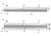
具体的な構成例について、図1を用いて以下に説明する。図1は、本実施形態の導電性基板の、透明基材、金属層、黒化層の積層方向と平行な面における断面図の例を示している。 A specific configuration example will be described below with reference to FIG. FIG. 1 shows an example of a cross-sectional view in a plane parallel to the stacking direction of the transparent base, the metal layer and the blackening layer of the conductive substrate of the present embodiment.
本実施形態の導電性基板は、例えば透明基材の少なくとも一方の面上に、透明基材側から金属層と、黒化層とがその順に積層された構造を有することができる。 The conductive substrate of the present embodiment can have, for example, a structure in which a metal layer and a blackening layer are laminated in this order from the transparent substrate side on at least one surface of the transparent substrate.
具体的な構成例について、図1、図2を用いて以下に説明する。図1、図2は、本実施形態の導電性基板の、透明基材、金属層、黒化層の積層方向と平行な面における断面図の例を示している。 A specific configuration example will be described below using FIGS. 1 and 2. 1 and 2 show an example of a cross-sectional view in a plane parallel to the stacking direction of the transparent base, the metal layer and the blackening layer of the conductive substrate of the present embodiment.
例えば、図1(a)に示した導電性基板10Aのように、透明基材11の一方の面11a側に金属層12と、黒化層13と、を一層ずつその順に積層することができる。また、図1(b)に示した導電性基板10Bのように、透明基材11の一方の面11a側と、もう一方の面(他方の面)11b側と、にそれぞれ金属層12A、12Bと、黒化層13A、13Bと、を一層ずつその順に積層することができる。
For example, as in the case of the
また、例えば透明基材11と、金属層12との間に密着層を設けた構成とすることもできる。例えば図2(a)に示した導電性基板20Aのように、透明基材11の一方の面11a側に、密着層14と、金属層12と、黒化層13と、をその順に積層することができる。
Further, for example, an adhesion layer may be provided between the
この場合も透明基材11の両面に密着層、金属層、黒化層を積層した構成とすることができる。具体的には図2(b)に示した導電性基板20Bのように、透明基材11の一方の面11a側と、もう一方の面(他方の面)11b側と、にそれぞれ密着層14A、14Bと、金属層12A、12Bと、黒化層13A、13Bと、をその順に積層できる。
Also in this case, the adhesion layer, the metal layer, and the blackening layer can be laminated on both surfaces of the
なお、透明基材の両面に金属層と、黒化層と、を積層した、図1(b)、図2(b)の構成例においては、透明基材11を対称面として透明基材11の上下に積層した層が対称になるように配置した例を示したが、係る形態に限定されるものではない。例えば、図2(b)において、透明基材11の一方の面11a側の構成を図1(a)の構成と同様に、金属層12と、黒化層13と、をその順に積層した形態とし、もう一方の面(他方の面)11b側を密着層14Bと、金属層12Bと、黒化層13Bと、をその順に積層した形態として、透明基材11の上下に積層した層を非対称な構成としてもよい。
In addition, in the structural example of FIG.1 (b) and FIG.2 (b) which laminated | stacked the metal layer and the blackening layer on both surfaces of a transparent base material, the
ここまで、本実施形態の導電性基板について説明してきたが、本実施形態の導電性基板においては、透明基材上に金属層と、黒化層と、を設けているため、金属層による光の反射を抑制することができる。従って、黒化層を設けることにより、例えばタッチパネル等に用いた場合に良好な視認性を有することができる。 So far, the conductive substrate of the present embodiment has been described, but in the conductive substrate of the present embodiment, since the metal layer and the blackening layer are provided on the transparent substrate, the light by the metal layer is obtained. Reflection can be suppressed. Therefore, by providing the blackening layer, for example, when used for a touch panel or the like, good visibility can be obtained.
本実施形態の導電性基板の光の反射の程度は特に限定されるものではないが、例えば波長400nm以上700nm以下の光の反射率の平均は10%以下であることが好ましく、8%以下であることがより好ましく、7%以下であることがさらに好ましい。これは波長400nm以上700nm以下の光の反射率の平均が10%以下の場合、例えばタッチパネル用の導電性基板として用いた場合でもディスプレイの視認性の低下を特に抑制できるためである。 The degree of reflection of light of the conductive substrate of the present embodiment is not particularly limited. For example, the average reflectance of light with a wavelength of 400 nm or more and 700 nm or less is preferably 10% or less, and 8% or less Is more preferably 7% or less. This is because when the average of the reflectance of light with a wavelength of 400 nm or more and 700 nm or less is 10% or less, a decrease in the visibility of the display can be particularly suppressed even when used as a conductive substrate for a touch panel, for example.
導電性基板の光の反射率の測定は、黒化層に光を照射するようにして測定を行うことができる。すなわち、導電性基板に含まれる金属層及び黒化層のうち、黒化層側から光を照射して測定を行うことができる。具体的には例えば図1(a)のように透明基材11の一方の面11aに金属層12、黒化層13の順に積層した場合、黒化層13に光を照射できるように、黒化層13の表面Aに対して光を照射して測定できる。
The light reflectance of the conductive substrate can be measured by irradiating the blackened layer with light. That is, measurement can be performed by irradiating light from the blackened layer side among the metal layer and the blackened layer contained in the conductive substrate. Specifically, for example, when the
なお、後述のように導電性基板は金属層及び黒化層をエッチングすることにより配線を形成できるが、上記反射率は導電性基板のうち透明基材を除いた場合に、最表面に配置されている黒化層の、光が入射する側の表面における反射率を示している。このため、エッチング処理前、または、エッチング処理を行った後であれば、金属層及び黒化層が残存している部分での測定値が上記範囲を満たしていることが好ましい。 In addition, although a conductive substrate can form wiring by etching a metal layer and a blackening layer as mentioned later, the said reflectance is arrange | positioned at the outermost surface, when a transparent base material is remove | excluded among conductive substrates. Shows the reflectance of the surface on the light incident side of the blackened layer. For this reason, it is preferable that the measurement value in the part in which the metal layer and the blackening layer remain | survive satisfy | fills the said range before an etching process or after performing an etching process.
なお、光の反射率の平均とは、400nm以上700nm以下の範囲内で波長を変化させて測定を行った際の測定結果の平均値を意味している。測定の際、波長を変化させる間隔は特に限定されないが、例えば、10nm毎に波長を変化させて上記波長範囲の光について測定を行うことが好ましく、1nm毎に波長を変化させて上記波長範囲の光について測定を行うことがより好ましい。 In addition, the average of the reflectance of light means the average value of the measurement result at the time of changing a wavelength within the range of 400 nm or more and 700 nm or less, and measuring. In the measurement, the interval for changing the wavelength is not particularly limited. For example, it is preferable to change the wavelength every 10 nm to measure the light in the above wavelength range, and change the wavelength every 1 nm to It is more preferred to make measurements on light.
本実施形態の導電性基板は上述のように例えばタッチパネル用の導電性基板として好ましく用いることができる。この場合、導電性基板は金属層、及び黒化層に開口部を備えた配線パターンが形成された構成とすることができる。より好ましくは、メッシュ状の配線を備えた構成とすることができる。 The conductive substrate of the present embodiment can be preferably used, for example, as a conductive substrate for a touch panel as described above. In this case, the conductive substrate can be configured to have a metal layer and a wiring pattern having an opening in the blackening layer. More preferably, a mesh-like wiring can be provided.
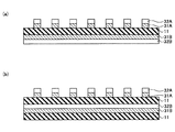
開口部を備えた配線パターンが形成された導電性基板は、ここまで説明した本実施形態の導電性基板の金属層及び黒化層をエッチングすることにより得ることができる。例えば、二層の配線によりメッシュ状の配線とすることができる。具体的な構成例を図3に示す。図3はメッシュ状の配線を備えた導電性基板30を金属層、黒化層の積層方向の上面側から見た図を示している。図3に示した導電性基板30は、透明基材11と、図中Y軸方向に平行な複数の配線31Aと、X軸方向に平行な配線31Bとを有している。なお、配線31A、31Bは金属層をエッチングして形成されており、該配線31A、31Bの上面または下面には図示しない黒化層が形成されている。また、黒化層は配線31A、31Bと同じ形状(パターン)にエッチングされている。
The conductive substrate on which the wiring pattern having the opening is formed can be obtained by etching the metal layer and the blackening layer of the conductive substrate of the present embodiment described above. For example, a two-layer wiring can be used to form a mesh-like wiring. A specific configuration example is shown in FIG. FIG. 3 is a view of the
透明基材11と配線31A、31Bとの配置は特に限定されない。透明基材11と配線との配置の構成例を図4(a)、(b)に示す。図4(a)、(b)は図3のA−A´線での断面図に当たる。
The arrangement of the
まず、図4(a)に示したように、透明基材11の上下面にそれぞれ配線31A、31Bが配置されていてもよい。なお、この場合、配線31Aの上面、及び配線31Bの下面には、配線と同じ形状にエッチングされた黒化層32A、32Bが配置されている。また、図4(b)に示したように、1組の透明基材11を用い、一方の透明基材11を挟んで上下面に配線31A、31Bを配置し、かつ、一方の配線31Bは透明基材11間に配置されてもよい。この場合も、配線31A、31Bの上面には配線と同じ形状にエッチングされた黒化層32A、32Bが配置されている。
First, as shown in FIG. 4A, the
なお、既述のように、金属層と、透明基材との間には密着層を設けることもできる。密着層を設ける場合、密着層についても配線と同様の形状となるようにエッチングされていることが好ましい。 As described above, an adhesive layer may be provided between the metal layer and the transparent substrate. When the adhesion layer is provided, it is preferable that the adhesion layer be etched to have the same shape as the wiring.
図3及び図4(a)に示したメッシュ状の配線を有する導電性基板は例えば、図1(b)のように透明基材11の両面に金属層12A、12Bと、黒化層13A、13Bと、を備えた導電性基板から形成できる。
For example, as shown in FIG. 1 (b), the conductive substrate having the mesh-like wiring shown in FIG. 3 and FIG. 4 (a) has
具体的にはまず、図1(b)に示した導電性基板の透明基材11の一方の面11a側の金属層12A及び黒化層13Aを、図1(b)中Y軸方向に平行な複数の線状のパターンが、X軸方向に沿って所定の間隔をあけて配置されるようにエッチングを行う。なお、図1(b)中のX軸方向とは、図1(b)中の各層の幅方向と平行な方向を意味している。また、Y軸方向とは、図1(b)中、紙面と垂直な方向を意味する。そして、透明基材11のもう一方の面11b側の金属層12B及び黒化層13Bを図1(b)中X軸方向と平行な複数の線状のパターンが、Y軸方向に沿って所定の間隔をあけて配置されるようにエッチングを行う。
Specifically, first, the
以上の操作により図3、図4(a)に示したメッシュ状の配線を有する導電性基板を形成することができる。なお、透明基材11の両面のエッチングは同時に行うこともできる。すなわち、金属層12A、12B、黒化層13A、13Bのエッチングは同時に行ってもよい。
By the above operation, the conductive substrate having the mesh-like wiring shown in FIG. 3 and FIG. 4A can be formed. In addition, the etching of both surfaces of the
また、図4(a)に示したメッシュ状の配線を有する導電性基板において、透明基材11と、配線31A、31Bとの間に密着層を設ける場合には、図1(b)に示した導電性基板に替えて、図2(b)に示した導電性基板を用いることができる。この場合、密着層14A、14Bについても金属層12A、12B等と同様にエッチングすることで得ることができる。
Further, in the case of providing an adhesive layer between the
図3に示したメッシュ状の配線を有する導電性基板は、図1(a)または図2(a)に示した導電性基板を2枚用いることにより形成することもできる。図1(a)の導電性基板を用いた場合を例に説明すると、図1(a)に示した導電性基板2枚についてそれぞれ、金属層12及び黒化層13を、X軸方向と平行な複数の線状のパターンが、Y軸方向に沿って所定の間隔をあけて配置されるようにエッチングを行う。そして、上記エッチング処理により各導電性基板に形成した線状のパターンが互いに交差するように向きをあわせて2枚の導電性基板を貼り合せることによりメッシュ状の配線を備えた導電性基板とすることができる。2枚の導電性基板を貼り合せる際に貼り合せる面は特に限定されるものではない。例えば図4(b)に示した構成とする場合、一方の導電性基板の金属層12等が積層された図1(a)における表面Aと、他方の導電性基板の金属層12等が積層されていない図1(a)における面11bとを貼り合せることができる。
The conductive substrate having the mesh-like wiring shown in FIG. 3 can also be formed by using two conductive substrates shown in FIG. 1 (a) or FIG. 2 (a). When the conductive substrate of FIG. 1A is used as an example, the
また、2枚の導電性基板を貼り合せて図4(a)に示した構成とする場合、例えば2枚の導電性基板について、透明基材11の金属層12等が積層されていない図1(a)における面11b同士を貼り合せることができる。
Further, in the case where two conductive substrates are bonded to form the configuration shown in FIG. 4A, for example, with respect to the two conductive substrates, the
図4(a)、または図4(b)に示した導電性基板において、透明基材11と、配線31A、31Bとの間に密着層を有する構成とする場合、図1(a)に示した導電性基板に替えて、図2(a)に示した導電性基板を用いることができる。
In the case where the conductive substrate shown in FIG. 4 (a) or FIG. 4 (b) has an adhesive layer between the
なお、図3、図4に示したメッシュ状の配線を有する導電性基板における配線の幅や、配線間の距離は特に限定されるものではなく、例えば、配線に流す電流量等に応じて選択することができる。 The width of the wires and the distance between the wires in the conductive substrate having the mesh-like wires shown in FIGS. 3 and 4 are not particularly limited, and may be selected according to, for example, the amount of current flowing through the wires. can do.
また、図3、図4においては、直線形状の配線を組み合わせてメッシュ状の配線(配線パターン)を形成した例を示しているが、係る形態に限定されるものではなく、配線パターンを構成する配線は任意の形状とすることができる。例えばディスプレイの画像との間でモアレ(干渉縞)が発生しないようメッシュ状の配線パターンを構成する配線の形状をそれぞれ、ぎざぎざに屈曲した線(ジグザグ直線)等の各種形状にすることもできる。 Moreover, although the example which formed mesh-like wiring (wiring pattern) combining the wiring of linear shape in FIG. 3, FIG. 4 is shown, it is not limited to the form which concerns, A wiring pattern is comprised The wiring can be of any shape. For example, the shapes of the wires forming the mesh-like wiring pattern may be various shapes such as lines (zigzag straight lines) bent in a jagged manner so as not to generate moire (interference fringes) with the image of the display.
このように2層の配線から構成されるメッシュ状の配線を有する導電性基板は、例えば投影型静電容量方式のタッチパネル用の導電性基板として好ましく用いることができる。 Thus, the conductive substrate having mesh-like wiring composed of two layers of wiring can be preferably used, for example, as a conductive substrate for a projected capacitive touch panel.
次に本実施形態の導電性基板の製造方法の一構成例について具体的に説明する。 Next, one configuration example of the method of manufacturing the conductive substrate of the present embodiment will be specifically described.
既述のように、本実施形態の導電性基板の製造方法は、透明基材の少なくとも一方の面上に金属層を形成する金属層形成工程と、金属層上に黒化層を形成する黒化層形成工程とを有することができる。各工程について以下に説明する。 As described above, in the method of manufacturing a conductive substrate according to the present embodiment, a metal layer forming step of forming a metal layer on at least one surface of a transparent substrate, and black forming a blackening layer on the metal layer And the step of forming a chemical layer. Each process is described below.
金属層形成工程に供する透明基材は予め準備しておくことができる。用いる透明基材の種類は特に限定されるものではないが、既述のように可視光を透過する樹脂基板(樹脂フィルム)や、ガラス基板等の透明基材を好ましく用いることができる。透明基材は必要に応じて予め任意のサイズに切断等行っておくこともできる。 The transparent substrate to be subjected to the metal layer forming step can be prepared in advance. The kind of transparent substrate to be used is not particularly limited, but as described above, a transparent substrate such as a resin substrate (resin film) that transmits visible light, a glass substrate, etc. can be preferably used. The transparent substrate can be cut into any size in advance, if necessary.
そして、金属層は既述のように、金属薄膜層を有することが好ましい。また、金属層は金属薄膜層と金属めっき層とを有することもできる。このため、金属層形成工程は、例えば乾式めっき法により金属薄膜層を形成するステップを有することができる。また、金属層形成工程は、乾式めっき法により金属薄膜層を形成するステップと、該金属薄膜層を給電層として、湿式めっき法の一種である電気めっき法により金属めっき層を形成するステップと、を有していてもよい。 The metal layer preferably has a metal thin film layer as described above. The metal layer can also have a metal thin film layer and a metal plating layer. Therefore, the metal layer forming step can include the step of forming the metal thin film layer by, for example, a dry plating method. In the metal layer forming step, a metal thin film layer is formed by a dry plating method, and a metal plating layer is formed by an electroplating method which is a kind of a wet plating method, using the metal thin film layer as a feeding layer. May be included.
金属薄膜層を形成するステップで用いる乾式めっき法としては、特に限定されるものではなく、例えば、蒸着法、スパッタリング法、又はイオンプレーティング法等を用いることができる。なお、蒸着法としては真空蒸着法を好ましく用いることができる。金属薄膜層を形成するステップで用いる乾式めっき法としては、特に膜厚の制御が容易であることから、スパッタリング法を用いることがより好ましい。 It does not specifically limit as a dry plating method used at the step which forms a metal thin film layer, For example, a vapor deposition method, sputtering method, or ion plating method etc. can be used. In addition, a vacuum evaporation method can be preferably used as an evaporation method. As the dry plating method used in the step of forming the metal thin film layer, it is more preferable to use the sputtering method because the control of the film thickness is particularly easy.
次に金属めっき層を形成するステップについて説明する。湿式めっき法により金属めっき層を形成するステップにおける条件、すなわち、電気めっき処理の条件は、特に限定されるものではなく、常法による諸条件を採用すればよい。例えば、金属めっき液を入れためっき槽に金属薄膜層を形成した基材を供給し、電流密度や、基材の搬送速度を制御することによって、金属めっき層を形成できる。 Next, the step of forming a metal plating layer will be described. The conditions in the step of forming the metal plating layer by the wet plating method, that is, the conditions of the electroplating treatment are not particularly limited, and various conditions according to the ordinary method may be adopted. For example, a metal plating layer can be formed by supplying a base having a metal thin film layer formed in a plating tank containing a metal plating solution and controlling the current density and the conveyance speed of the base.
金属層に好適に用いることができる材料や、金属層の好適な厚さ等については既述のため、ここでは説明を省略する。 The material that can be suitably used for the metal layer, the preferable thickness of the metal layer, and the like have already been described, and thus the description thereof is omitted here.
次に、黒化層形成工程について説明する。 Next, the blackening layer forming step will be described.
黒化層形成工程は、以下のステップを有することができる。 The blackening layer forming step can have the following steps.
ニッケルと銅と酸素とを含有する黒化層を形成する黒化層形成ステップ。
黒化層の表面と、酸含有水溶液とを接触させる表面処理ステップ。
A blackening layer forming step of forming a blackening layer containing nickel, copper and oxygen.
A surface treatment step of bringing the surface of the blackening layer into contact with an acid-containing aqueous solution.
まず、黒化層形成ステップについて説明する。 First, the blackening layer forming step will be described.
黒化層形成ステップでは、既述のように、Niと、Cuと、Oとを含有する黒化層を形成することができる。 In the blackening layer forming step, as described above, the blackening layer containing Ni, Cu, and O can be formed.
黒化層形成ステップでの黒化層の成膜方法は特に限定されるものではないが、黒化層は乾式法により成膜されることが好ましい。 Although the film forming method of the blackened layer in the blackened layer forming step is not particularly limited, it is preferable that the blackened layer is formed by a dry method.
黒化層を乾式法により成膜する場合、その具体的な方法は特に限定されるものではないが、例えばスパッタリング法、イオンプレーティング法や蒸着法等の乾式めっき法を好ましく用いることができる。黒化層を乾式法により成膜する場合、膜厚の制御が容易であることから、スパッタリング法を用いることがより好ましい。 When forming a blackening layer into a film by a dry method, the specific method is not specifically limited, For example, dry-plating methods, such as a sputtering method, an ion plating method, a vapor deposition method, can be used preferably. When forming a blackening layer into a film by a dry process, since control of a film thickness is easy, it is more preferable to use sputtering method.
なお、黒化層は上述のように酸素を含有することができるため、反応性スパッタリング法により成膜されることが特に好ましい。 In addition, since the blackening layer can contain oxygen as described above, it is particularly preferable to form a film by reactive sputtering.
反応性スパッタリング法により黒化層を成膜する場合、ターゲットとしては、黒化層を構成するNiと、Cuとを含有するターゲットを用いることができる。例えば、Ni−Cu合金のターゲットを好ましく用いることができる。ターゲットの組成は特に限定されるものではないが、例えばNi−Cu合金のターゲットを用いる場合、Niの含有量が30質量%以上80質量%以下であることが好ましく、50質量%以上80質量%以下であることがより好ましい。 In the case of forming a blackened layer by reactive sputtering, a target containing Ni and Cu constituting the blackened layer can be used as a target. For example, a target of a Ni-Cu alloy can be preferably used. The composition of the target is not particularly limited. For example, when using a target of a Ni-Cu alloy, the content of Ni is preferably 30% by mass to 80% by mass, and 50% by mass to 80% by mass It is more preferable that
そして、黒化層を成膜する際の不活性ガス中に酸素を添加することにより、Niと、Cuと、Oとを含有する黒化層を形成することができる。なお、不活性ガスについても特に限定されないが、例えばアルゴンを好ましく用いることができる。 Then, by adding oxygen to the inert gas when forming the blackening layer, it is possible to form a blackening layer containing Ni, Cu and O. The inert gas is also not particularly limited, but, for example, argon can be preferably used.
黒化層の好適な厚さ等については既述のため、ここでは説明を省略する。 About the suitable thickness of a blackening layer, etc., since it is stated above, explanation is omitted here.
次に表面処理ステップについて説明する。 Next, the surface treatment step will be described.
表面処理ステップでは、黒化層形成ステップで形成した黒化層の表面と、酸含有水溶液とを接触させることができる。 In the surface treatment step, the surface of the blackened layer formed in the blackened layer forming step can be brought into contact with the acid-containing aqueous solution.
このように、形成した黒化層の表面を酸含有水溶液により表面処理することで、黒化層の反射率を低く抑制し、かつ黒化層のエッチング液に対する反応性、すなわちエッチング性を高めることが可能になる。このため、低反射率と、エッチング性とを両立した黒化層とすることができる。 Thus, by treating the surface of the formed blackened layer with an aqueous solution containing an acid, the reflectance of the blackened layer is suppressed low and the reactivity of the blackened layer to the etching solution, that is, the etching property is enhanced. Becomes possible. For this reason, it is possible to provide a blackened layer in which low reflectance and etching properties are compatible.
酸含有水溶液による表面処理により、低反射率と、エッチング性とが両立した黒化層となる理由は明らかではないが、黒化層に含まれるニッケルおよび/または銅が酸含有水溶液に選択的に溶解して、黒化層の表面をミクロに荒らしているためと考えられる。 It is not clear why the surface treatment with an acid-containing aqueous solution results in a blackened layer in which low reflectance and etching properties are compatible, but nickel and / or copper contained in the blackened layer is selectively used for the acid-containing aqueous solution. It is thought that it melts and roughens the surface of the blackened layer to micro.
具体的には、黒化層の表面がミクロに荒れることで黒化層表面で光が乱反射し易くなるため、反射率を低減できると考えられる。また、黒化層の表面がミクロに荒れることで、黒化層の表面の面積が増大し、エッチング液との反応性を高めることができると考えられる。このため、上述のように、低反射率と、エッチング性とを両立した黒化層とすることができる。 Specifically, since the light is easily irregularly reflected on the surface of the blackened layer by roughening the surface of the blackened layer to a micro size, it is considered that the reflectance can be reduced. In addition, it is considered that the surface area of the blackened layer can be increased and the reactivity with the etching solution can be enhanced by roughening the surface of the blackened layer to micro. For this reason, as described above, it is possible to provide a blackened layer in which low reflectance and etchability are compatible.
酸含有水溶液については、その組成は特に限定されるものではないが、塩酸および/または硫酸を含有することが好ましく、塩酸および/または硫酸と、水とから構成されていることがより好ましい。 The composition of the acid-containing aqueous solution is not particularly limited, but preferably contains hydrochloric acid and / or sulfuric acid, and is more preferably composed of hydrochloric acid and / or sulfuric acid and water.
酸含有水溶液としては、例えば塩酸を含有する塩酸含有水溶液を好ましく用いることができる。塩酸含有水溶液は、塩酸の濃度が1.0質量%以上10.0質量%以下であることが好ましく、1.5質量%以上8.0質量%以下であることがより好ましい。 As the acid-containing aqueous solution, for example, a hydrochloric acid-containing aqueous solution containing hydrochloric acid can be preferably used. The concentration of hydrochloric acid in the hydrochloric acid-containing aqueous solution is preferably 1.0% by mass or more and 10.0% by mass or less, and more preferably 1.5% by mass or more and 8.0% by mass or less.
これは塩酸含有水溶液の塩酸濃度を1.0質量%以上とすることで、黒化層の反射率を特に低く抑制することができるからである。ただし、塩酸含有水溶液の塩酸濃度が10.0質量%を超えると、黒化層の表面の色が黒色から赤褐色等に変色する場合があるため、上述のように10.0質量%以下であることが好ましい。 This is because the reflectance of the blackened layer can be suppressed to a particularly low level by setting the hydrochloric acid concentration of the aqueous solution containing hydrochloric acid to 1.0 mass% or more. However, if the concentration of hydrochloric acid in the aqueous solution containing hydrochloric acid exceeds 10.0% by mass, the color of the surface of the blackened layer may change from black to reddish brown etc., so it is 10.0% by mass or less as described above Is preferred.
また、酸含有水溶液としては、硫酸を含有する硫酸含有水溶液も好ましく用いることができる。硫酸含有水溶液は、硫酸の濃度が15.0質量%以下であることが好ましく、12.0質量%以下であることがより好ましい。 Moreover, as an acid containing aqueous solution, the sulfuric acid containing aqueous solution containing a sulfuric acid can also be used preferably. The concentration of sulfuric acid in the sulfuric acid-containing aqueous solution is preferably 15.0% by mass or less, and more preferably 12.0% by mass or less.
これは、硫酸含有水溶液の硫酸濃度を15.0質量%以下とすることで、黒化層の表面の色が黒色から、他の色に変色することを抑制しつつ、黒化層の反射率を低く抑制し、エッチング性を高めることができるからである。 This is the reflectance of the blackened layer while suppressing the color of the surface of the blackened layer from changing from black to another color by setting the sulfuric acid concentration of the aqueous solution containing sulfuric acid to 15.0% by mass or less Can be suppressed low, and the etching property can be enhanced.
なお、硫酸の濃度の下限値は特に限定されるものではないが、例えば1.0質量%以上であることが好ましく、5.0質量%以上であることがより好ましい。 The lower limit value of the concentration of sulfuric acid is not particularly limited, but is preferably, for example, 1.0% by mass or more, and more preferably 5.0% by mass or more.
なお、酸含有水溶液としては、塩酸と、硫酸とを含有する水溶液も用いることができる。この場合、塩酸の濃度が1.0質量%以上10.0質量%以下であり、硫酸の濃度が15.0質量%以下であることが好ましい。 An aqueous solution containing hydrochloric acid and sulfuric acid can also be used as the acid-containing aqueous solution. In this case, the concentration of hydrochloric acid is preferably 1.0% by mass or more and 10.0% by mass or less, and the concentration of sulfuric acid is preferably 15.0% by mass or less.
塩酸と、硫酸とを含有する酸含有水溶液においては、塩酸の濃度は1.5質量%以上8.0質量%以下であることがより好ましく、硫酸の濃度は12.0質量%以下であることがより好ましい。なお、硫酸の濃度の下限値は特に限定されないが、例えば1.0質量%以上であることが好ましく、5.0質量%以上であることがより好ましい。 In the acid-containing aqueous solution containing hydrochloric acid and sulfuric acid, the concentration of hydrochloric acid is more preferably 1.5% by mass or more and 8.0% by mass or less, and the concentration of sulfuric acid is 12.0% by mass or less Is more preferred. The lower limit value of the concentration of sulfuric acid is not particularly limited, but is preferably, for example, 1.0% by mass or more, and more preferably 5.0% by mass or more.
黒化層の表面と、酸含有水溶液とを接触させる方法は特に限定されるものではない。 The method for bringing the surface of the blackening layer into contact with the acid-containing aqueous solution is not particularly limited.
例えば透明基材の少なくとも一方の面側に黒化層を形成した基材を、酸含有水溶液に浸漬することで、黒化層の表面と、酸含有水溶液とを接触させることができる。 For example, the surface of the blackened layer can be brought into contact with the acid-containing aqueous solution by immersing the substrate having the blackened layer formed on at least one surface side of the transparent substrate in the acid-containing aqueous solution.
また、例えば黒化層の表面に、酸含有水溶液を供給、塗布することで、黒化層の表面と、酸含有水溶液とを接触させることもできる。この場合、酸含有水溶液を供給、塗布する手段、方法は特に限定されないが、例えばスプレー等を用いることができる。 Further, for example, the acid-containing aqueous solution can be brought into contact with the surface of the blackened layer by supplying and applying the acid-containing aqueous solution to the surface of the blackened layer. In this case, the means and method for supplying and applying the acid-containing aqueous solution are not particularly limited. For example, a spray or the like can be used.
黒化層の表面と、酸含有水溶液とを接触させる時間は特に限定されるものではないが、黒化層の表面と、酸含有水溶液とが十分に反応するように、5秒以上接触させておくことが好ましく、10秒以上接触させておくことが好ましい。 The time for bringing the surface of the blackening layer into contact with the acid-containing aqueous solution is not particularly limited, but the contact of the surface of the blackening layer with the acid-containing aqueous solution is sufficient for 5 seconds or more. It is preferable to keep them in contact for 10 seconds or more.
黒化層の表面と、酸含有水溶液とを接触させる時間の上限は特に限定されるものではないが、例えば生産性の観点から、60秒以下であることが好ましく、45秒以下であることがより好ましい。 The upper limit of the time for which the surface of the blackening layer is in contact with the acid-containing aqueous solution is not particularly limited, but is preferably 60 seconds or less and 45 seconds or less from the viewpoint of productivity, for example. More preferable.
なお、黒化層の表面と酸含有水溶液とを接触させる時間とは、例えば黒化層を形成した基材を酸含有水溶液に浸漬する場合、該基材を酸含有水溶液に浸漬してから、該基材を取り出し水洗等により酸含有水溶液を除去するまでの時間をいう。また、例えば黒化層の表面に、酸含有水溶液を供給、塗布する場合であれば、黒化層の表面に酸含有水溶液を供給、塗布し始めてから、水洗等により酸含有水溶液を除去するまでの時間をいう。 The time for which the surface of the blackening layer is in contact with the acid-containing aqueous solution is, for example, when the substrate on which the blackening layer is formed is immersed in the acid-containing aqueous solution, after immersing the substrate in the acid-containing aqueous solution, The time until the base material is taken out and the acid-containing aqueous solution is removed by washing with water etc. For example, in the case of supplying and applying an acid-containing aqueous solution to the surface of the blackened layer, the acid-containing aqueous solution is supplied and applied to the surface of the blackened layer and then the acid-containing aqueous solution is removed by washing with water. Time for
表面処理ステップを終了後は、黒化層の表面に供給した酸含有水溶液を除去するため、例えば、表面処理ステップに供した、透明基材の少なくとも一方の面側に黒化層を形成した基材を水洗、乾燥する水洗、乾燥ステップを実施できる。 After the surface treatment step is completed, in order to remove the acid-containing aqueous solution supplied to the surface of the blackened layer, for example, a group having the blackened layer formed on at least one surface of the transparent substrate which has been subjected to the surface treatment step. The material can be washed with water and dried, followed by washing and drying steps.
水洗、乾燥ステップにおいては、例えばまず、表面処理ステップに供した、透明基材の少なくとも一方の面側に黒化層を形成した基材を水洗することができる。水洗の方法は特に限定されないが、例えば該基材を水を入れた水槽内に供給し、該水槽内を搬送することで洗浄することができる。また、該基材に対して、スプレー等により水を供給し水洗することもできる。 In the washing with water and drying steps, for example, the base having the blackened layer formed on at least one side of the transparent base, which has been subjected to the surface treatment step, can be washed with water. Although the method of washing with water is not particularly limited, for example, the substrate can be supplied into a water tank containing water, and can be washed by transporting the inside of the water tank. In addition, water can be supplied to the base material by spraying or the like to wash the base material.
そして、水洗後に乾燥する方法についても特に限定されないが、例えばドライヤー等により乾燥することができる。なお、水洗と乾燥との間に、基材に付着した水分を除去する水切り等を実施することもできる。 And although it does not specifically limit about the method to dry after water washing, for example, it can dry with a dryer etc. In addition, draining etc. which remove the water | moisture content which adhered to the base material can also be implemented between water washing and drying.
ここまで、金属層形成工程と、黒化層形成工程について説明してきたが、本実施形態の導電性基板の製造方法においては、上述の工程に加えてさらに任意の工程を実施することもできる。 So far, the metal layer forming step and the blackening layer forming step have been described. However, in the method of manufacturing a conductive substrate of the present embodiment, an optional step can be performed in addition to the above-described steps.
例えば透明基材と金属層との間に密着層を形成する場合、透明基材の金属層を形成する面上に密着層を形成する密着層形成工程を実施することができる。密着層形成工程を実施する場合、金属層形成工程は、密着層形成工程の後に実施することができ、金属層形成工程では、本工程で透明基材上に密着層を形成した基材に金属薄膜層を形成できる。 For example, when forming an adhesion layer between a transparent base material and a metal layer, an adhesion layer formation process which forms an adhesion layer on the field which forms a metal layer of a transparent base material can be carried out. When the adhesion layer formation step is carried out, the metal layer formation step can be carried out after the adhesion layer formation step, and in the metal layer formation step, metal is formed on the base on which the adhesion layer is formed on the transparent substrate in this step. A thin film layer can be formed.
密着層形成工程において、密着層の成膜方法は特に限定されるものではないが、乾式めっき法により成膜することが好ましい。乾式めっき法としては例えばスパッタリング法、イオンプレーティング法や蒸着法等を好ましく用いることができる。密着層を乾式法により成膜する場合、膜厚の制御が容易であることから、スパッタリング法を用いることがより好ましい。なお、密着層には既述のように炭素、酸素、水素、窒素から選ばれる1種類以上の元素を添加することもでき、この場合は反応性スパッタリング法をさらに好ましく用いることができる。 In the adhesion layer forming step, the film formation method of the adhesion layer is not particularly limited, but it is preferable to form a film by a dry plating method. As the dry plating method, for example, a sputtering method, an ion plating method, a vapor deposition method and the like can be preferably used. In the case where the adhesion layer is formed by a dry method, it is more preferable to use a sputtering method because control of the film thickness is easy. As described above, one or more elements selected from carbon, oxygen, hydrogen and nitrogen can be added to the adhesion layer, and in this case, reactive sputtering can be more preferably used.
密着層に好適に用いることができる材料や、密着層の好適な厚さ等については既述のため、ここでは説明を省略する。 The material that can be suitably used for the adhesion layer, the preferable thickness of the adhesion layer, and the like have already been described, and thus the description thereof is omitted here.
本実施形態の導電性基板の製造方法で得られる導電性基板は例えばタッチパネル等の各種用途に用いることができる。そして、各種用途に用いる場合には、本実施形態の導電性基板に含まれる金属層、及び黒化層がパターン化されていることが好ましい。なお、密着層を設ける場合は、密着層についてもパターン化されていることが好ましい。金属層、黒化層、場合によってはさらに密着層は、例えば所望の配線パターンにあわせてパターン化することができ、金属層、黒化層、場合によってはさらに密着層は同じ形状にパターン化されていることが好ましい。 The conductive substrate obtained by the method for producing a conductive substrate of the present embodiment can be used, for example, in various applications such as a touch panel. And when using for various uses, it is preferable that the metal layer contained in the conductive substrate of this embodiment, and a blackening layer are patterned. When the adhesion layer is provided, it is preferable that the adhesion layer is also patterned. The metal layer, the blackening layer and possibly also the adhesion layer can be patterned, for example, in accordance with the desired wiring pattern, and the metal layer, the blackening layer and possibly also the adhesion layer are patterned in the same shape Is preferred.
このため、本実施形態の導電性基板の製造方法は、金属層、及び前記黒化層を配線パターンに応じてエッチングする配線加工工程をさらに有することができる。なお、密着層を形成した場合には、配線加工工程では、密着層、金属層、及び黒化層を配線パターンに応じてエッチングすることができる。 Therefore, the method of manufacturing the conductive substrate of the present embodiment can further include a wiring processing step of etching the metal layer and the blackening layer in accordance with the wiring pattern. When the adhesion layer is formed, the adhesion layer, the metal layer, and the blackening layer can be etched according to the wiring pattern in the wiring process.
配線加工工程の具体的手順は特に限定されるものではなく、任意の手順により実施することができる。例えば図1(a)のように透明基材11上に金属層12、黒化層13が積層された導電性基板10Aの場合、まず黒化層13上の表面Aに所望のパターンを有するマスクを配置するマスク配置ステップを実施することができる。なお、所望のパターンを有するマスクの形成方法は特に限定されないが、配線パターン等に応じて例えばフォトリソグラフィー法等、従来の技術と同様の方法により形成することができる。
The specific procedure of the wiring process is not particularly limited, and can be implemented by any procedure. For example, in the case of the
次いで、黒化層13の表面A、すなわち、マスクを配置した面側にエッチング液を供給するエッチングステップを実施できる。
Then, an etching step may be performed in which the etchant is supplied to the surface A of the
エッチングステップにおいて用いるエッチング液は特に限定されるものではないが、本実施形態の導電性基板は、エッチング性に優れた黒化層を有するため、銅層と同様のエッチング液への反応性を示す。このため、配線加工工程で用いるエッチング液は特に限定されるものではなく、一般的に銅層のエッチングに用いられるエッチング液を好ましく用いることができる。 Although the etching solution used in the etching step is not particularly limited, the conductive substrate of the present embodiment exhibits the same reactivity to the etching solution as the copper layer because it has a blackened layer excellent in etching property. . Therefore, the etching solution used in the wiring processing step is not particularly limited, and an etching solution generally used for etching a copper layer can be preferably used.
エッチング工程で用いるエッチング液としては例えば、硫酸、過酸化水素水、塩酸、塩化第二銅、及び塩化第二鉄から選択された1種類を含む水溶液、または上記硫酸等から選択された2種類以上を含む混合水溶液をより好ましく用いることができる。エッチング液中の各成分の含有量は、特に限定されるものではない。 As an etching solution used in the etching step, for example, an aqueous solution containing one selected from sulfuric acid, hydrogen peroxide water, hydrochloric acid, cupric chloride, and ferric chloride, or two or more types selected from the above sulfuric acid and the like More preferably, a mixed aqueous solution containing The content of each component in the etching solution is not particularly limited.
エッチング液は室温で用いることもできるが、反応性を高めるため加温して用いることもでき、例えば40℃以上50℃以下に加熱して用いることができる。 The etching solution can be used at room temperature, but can also be used by heating to enhance the reactivity, for example, it can be used by heating to 40 ° C. or more and 50 ° C. or less.
また、図1(b)のように透明基材11の一方の面11a、他方の面11bに金属層12A、12B、黒化層13A、13Bを積層した導電性基板10Bの場合でも、各層について所望の配線パターンに応じてエッチングする配線加工工程を実施できる。
Further, even in the case of the
図1(b)に示した導電性基板の場合、例えば黒化層13A、13B上の表面A、及び表面Bに所望のパターンを有するマスクを配置するマスク配置ステップを実施できる。次いで、黒化層13A、13B上の表面A、及び表面B、すなわち、マスクを配置した面側にエッチング液を供給するエッチングステップを実施できる。
In the case of the conductive substrate shown in FIG. 1B, for example, a mask disposing step of disposing a mask having a desired pattern on the surface A and the surface B on the blackened
エッチングステップで形成するパターンについては特に限定されるものではなく、所望の配線パターンに応じた任意の形状とすることができる。例えば既述のように、2層の配線によりメッシュ状の配線を備えた導電性基板とすることもできる。 The pattern to be formed in the etching step is not particularly limited, and can have any shape according to the desired wiring pattern. For example, as described above, the conductive substrate can also be provided with a mesh-like wiring by two layers of wiring.
また、配線加工工程で例えば図1(a)に示した導電性基板10Aについて金属層12、黒化層13をエッチングした後、得られた2枚以上の導電性基板を積層する積層工程を実施することもできる。積層する際、例えば各導電性基板の配線パターンが交差するように積層することにより、メッシュ状の配線を備えた積層導電性基板を得ることもできる。
In addition, after the
積層した2枚以上の導電性基板を固定する方法は特に限定されるものではないが、例えば接着剤等により固定することができる。 Although the method of fixing the laminated two or more conductive substrates is not particularly limited, for example, it can be fixed by an adhesive or the like.
以上の本実施形態の導電性基板の製造方法により得られる導電性基板は、酸含有水溶液により表面処理を施された、ニッケルと、銅と、酸素とを含有する黒化層を備えている。このため、低反射率と、エッチング性とを両立した黒化層を備えた導電性基板とすることができる。 The conductive substrate obtained by the method for producing a conductive substrate of the present embodiment described above includes a blackened layer containing nickel, copper and oxygen which has been subjected to a surface treatment with an aqueous solution containing an acid. Therefore, it is possible to obtain a conductive substrate provided with a blackened layer in which low reflectance and etching property are compatible.
以下に具体的な実施例、比較例を挙げて説明するが、本発明はこれらの実施例に限定されるものではない。
(1)評価方法
まず、得られた導電性基板の評価方法について説明する。
(黒化層の外観の評価)
得られた導電性基板の黒化層について、外観を目視により評価した。
The present invention will be described by way of specific examples and comparative examples, but the present invention is not limited to these examples.
(1) Evaluation Method First, an evaluation method of the obtained conductive substrate will be described.
(Evaluation of the appearance of the blackened layer)
The appearance of the resulting blackened layer of the conductive substrate was evaluated by visual observation.
黒化層の色が黒色の場合には◎と評価し、黒色以外場合には×と評価した。 When the color of the blackened layer was black, it was evaluated as ◎, and when it was not black, it was evaluated as x.
(波長400nm以上700nm以下の光の平均反射率)
測定は、紫外可視分光光度計(株式会社 島津製作所製 型式:UV−2600)に反射率測定ユニットを設置して行った。
(Average reflectance of light with a wavelength of 400 nm to 700 nm)
The measurement was performed by installing a reflectance measurement unit in an ultraviolet-visible spectrophotometer (manufactured by Shimadzu Corporation, model: UV-2600).
以下の各実験例で作製した、図1(a)に示した構造の導電性基板の黒化層13の表面Aに対して、入射角5°、受光角5°として、波長400nm以上700nm以下の光を波長400nmから波長1nm間隔で変化させて照射して各波長での正反射率を測定した。そして、測定した全波長での反射率の平均値を該導電性基板の波長400nm以上700nm以下の光の平均反射率(正反射率)とした。
(エッチング試験)
エッチング試験では塩化第二鉄を10重量%、塩酸を1重量%、残部は水からなるエッチング液を用いた。
With respect to the surface A of the blackened
(Etching test)
In the etching test, an etchant containing 10% by weight of ferric chloride, 1% by weight of hydrochloric acid, and the balance of water was used.
各実験例で作製した導電性基板を、レジスト等は形成せずに、温度25℃のエッチング液中に60sec浸漬した後、エッチング液から取り出した。そしてその後、水洗により導電性基板に付着したエッチング液を十分に洗い流した。 The conductive substrate produced in each experimental example was immersed in an etching solution at a temperature of 25 ° C. for 60 seconds without forming a resist or the like, and then removed from the etching solution. After that, the etching solution adhering to the conductive substrate was sufficiently washed away by water washing.
エッチング液に浸漬、水洗した後の導電性基板を目視により観察し、透明基材上に残った金属層および黒化層の有無を観察した。 The conductive substrate after immersion in an etching solution and washing with water was visually observed, and the presence or absence of the metal layer and the blackened layer remaining on the transparent substrate was observed.
金属層および黒化層が残存しない場合、すなわち残渣が確認できない場合には、黒化層がエッチング性に優れ、同時にエッチングできる金属層、および黒化層を備えた導電性基板であることを示している。 In the case where the metal layer and the blackening layer do not remain, that is, when the residue can not be confirmed, it is indicated that the blackening layer is a conductive layer provided with a metal layer excellent in etching properties and capable of etching simultaneously and a blackening layer. ing.
これに対して金属層と、黒化層との少なくとも一方が残存している場合、すなわち残渣が確認できた場合には、黒化層のエッチング性が低く、成膜した金属層および黒化層を同時にエッチングできないことを示している。
(2)試料の作製条件、評価結果
以下に説明する条件で各実験例の導電性基板を作製し、上述の評価方法により評価を行った。
[実験例1]
以下に示すように、実験例1−1〜実験例1−7の試料を作製し、評価を行った。
(実験例1−1)
(金属層形成工程)
まず、長さ100m、幅500mm、厚さ50μmのポリエチレンテレフタレート樹脂(PET)製の透明基材を用意した。なお、透明基材として用いたポリエチレンテレフタレート樹脂製の透明基材について、全光線透過率をJIS K 7361−1に規定された方法により評価を行ったところ97%であった。
On the other hand, when at least one of the metal layer and the blackening layer remains, that is, when the residue can be confirmed, the etchability of the blackening layer is low, and the deposited metal layer and the blackening layer are formed. Indicates that it is impossible to etch at the same time.
(2) Preparation conditions of a sample, evaluation result The conductive substrate of each experimental example was produced on the conditions explained below, and evaluation was performed by the above-mentioned evaluation method.
[Experimental Example 1]
As shown below, samples of Experimental Example 1-1 to Experimental Example 1-7 were prepared and evaluated.
(Experimental example 1-1)
(Metal layer formation process)
First, a transparent substrate made of polyethylene terephthalate resin (PET) having a length of 100 m, a width of 500 mm, and a thickness of 50 μm was prepared. In addition, it was 97% when the total light transmittance was evaluated by the method prescribed | regulated to JISK7361-1 about the transparent substrate made from the polyethylene terephthalate resin used as a transparent substrate.
そして、銅ターゲットを装着したスパッタリング装置により、透明基材の一方の主平面上に金属層として、銅層(銅薄膜層)を形成した。 Then, using a sputtering apparatus equipped with a copper target, a copper layer (copper thin film layer) was formed as a metal layer on one main plane of the transparent substrate.
金属層は、まず上述の透明基材をセットしたチャンバー内を1×10⁻⁴Paまで排気した後、アルゴンガスを導入し、チャンバー内の圧力が1.3Paになるように調整した。そして、銅ターゲットに電力を供給し、透明基材上に厚さ0.5μmの銅層を形成した。
(黒化層形成工程)
まず、以下の手順により、ニッケルと、銅と、酸素とを含有する黒化層を形成する黒化層形成ステップを実施した。
The metal layer was first evacuated to 1 × 10 −4 Pa in a chamber in which the above-mentioned transparent substrate was set, and then argon gas was introduced to adjust the pressure in the chamber to 1.3 Pa. Then, power was supplied to the copper target to form a copper layer having a thickness of 0.5 μm on the transparent substrate.
(Blackening layer formation process)
First, the blackened layer forming step of forming a blackened layer containing nickel, copper, and oxygen was performed according to the following procedure.
スパッタリング装置に、ニッケル65質量%と、銅35質量%とを含有するニッケル−銅合金のターゲットを装着した。 The sputtering apparatus was equipped with a nickel-copper alloy target containing 65% by mass of nickel and 35% by mass of copper.
そして、該スパッタリング装置のチャンバー内に、上述の金属層形成工程で、透明基材上に金属層を形成した基材を、ターゲットと、金属層とが対向するように設置した。 Then, in the chamber of the sputtering apparatus, the base on which the metal layer was formed on the transparent base in the above-described metal layer forming step was placed such that the target and the metal layer were opposed to each other.
次いで、チャンバー内を1×10⁻⁴Paまで排気した後、アルゴンガスと、酸素ガスとを導入し、チャンバー内の圧力が2.0Paになるように調整した。なお、この際、チャンバー内のアルゴンガスと、酸素ガスとの混合ガス中の酸素ガスの割合が10体積%となるようにアルゴンガスと、酸素ガスとを供給した。 Subsequently, after exhausting the inside of a chamber to 1 * 10 <-4> Pa, argon gas and oxygen gas were introduce | transduced and it adjusted so that the pressure in a chamber might be 2.0 Pa. At this time, argon gas and oxygen gas were supplied such that the ratio of oxygen gas in the mixed gas of argon gas and oxygen gas in the chamber was 10% by volume.
そして、ニッケル−銅合金のターゲットに電力を供給し、金属層上に厚さ50nmの黒化層を形成した。 Then, power was supplied to the nickel-copper alloy target to form a blackened layer having a thickness of 50 nm on the metal layer.
次いで、表面処理ステップを実施した。 A surface treatment step was then performed.
表面処理ステップでは、塩酸と、水とからなり、塩酸濃度が1.5質量%である酸含有水溶液に、室温で15秒間浸漬した。 In the surface treatment step, the substrate was immersed for 15 seconds at room temperature in an acid-containing aqueous solution consisting of hydrochloric acid and water and having a hydrochloric acid concentration of 1.5% by mass.
表面処理ステップ終了後は、得られた導電性基板を水洗し、乾燥させる、水洗、乾燥ステップを実施した。 After completion of the surface treatment step, the obtained conductive substrate was washed with water and dried.
水洗、乾燥ステップでは、導電性基板の表面にスプレーで水を吹き付け、水洗を行い、水洗ステップで導電性基板に付着した水を切る水切りを行った後、ドライヤーで乾燥させることで、水洗、乾燥を行った。 In the water washing and drying steps, the surface of the conductive substrate is sprayed with water by spraying to wash the water, and in the water washing step, the water adhering to the conductive substrate is drained off, and then dried by a dryer. Did.
得られた導電性基板について、上述の黒化層の外観の評価、及び波長400nm以上700nm以下の光の平均反射率の測定を実施した。結果を表1に示す。 About the obtained conductive substrate, evaluation of the external appearance of the above-mentioned blackening layer and measurement of the average reflectance of light with a wavelength of 400 nm or more and 700 nm or less were performed. The results are shown in Table 1.
また、エッチング試験を実施したところ残渣がないことを確認できた。
(実験例1−2〜実験例1−7)
実験例1−2〜実験例1−6については、表面処理ステップにおいて、塩酸と、水とからなり、塩酸濃度が表1に示した値である酸含有水溶液を各実験例で用いた点以外は、実験例1−1と同様にして導電性基板を作製、評価した。評価結果を表1に示す。
Moreover, when the etching test was implemented, it has confirmed that there was no residue.
(Experimental Example 1-2 to Experimental Example 1-7)
In Experimental Examples 1-2 to 1-6, in the surface treatment step, an acid-containing aqueous solution consisting of hydrochloric acid and water and having a hydrochloric acid concentration shown in Table 1 was used in each experimental example. In the same manner as in Experiment Example 1-1, a conductive substrate was produced and evaluated. The evaluation results are shown in Table 1.
実験例1−7については、表面処理ステップを実施しなかった点以外は、実験例1−1と同様にして導電性基板を作製した。得られた導電性基板について、上述の黒化層の外観の評価、及び波長400nm以上700nm以下の光の平均反射率の測定を実施した。評価結果を表1に示す。 In Experimental Example 1-7, a conductive substrate was produced in the same manner as in Experimental Example 1-1 except that the surface treatment step was not performed. About the obtained conductive substrate, evaluation of the external appearance of the above-mentioned blackening layer and measurement of the average reflectance of light with a wavelength of 400 nm or more and 700 nm or less were performed. The evaluation results are shown in Table 1.
また、エッチング試験を実施したところ、いずれの実験例でも残渣がないことを確認できた。 Moreover, when the etching test was implemented, it was able to confirm that there is no residue in any experiment example.

これに対して、実験例1−7については、反射率が10.2%と高くなっており、反射率(平均反射率)を十分に低くした黒化層が得られていないことを確認できた。 On the other hand, in Experimental Example 1-7, the reflectance is as high as 10.2%, and it can be confirmed that a blackened layer having a sufficiently low reflectance (average reflectance) can not be obtained. The
なお、実験例1−6においては、黒化層の外観の評価の結果、不良となることが確認できた。係る結果から、表面処理ステップで、酸含有水溶液として塩酸含有水溶液を用いる場合には、塩酸の濃度が10質量%以下であることが好ましいことを確認できた。
[実験例2]
(実験例2−1〜実験例2−4)
表面処理ステップにおいて、各実験例で、表1に示した硫酸を含有する酸含有水溶液を用いた点以外は、実験例1−1と同様にして導電性基板を作製した。なお、実験例2−1では、硫酸と、水とからなる酸含有水溶液を用い、実験例2−2〜実験例2−4では、硫酸と、塩酸と、水とからなる酸含有水溶液を用いている。
In Experimental Example 1-6, as a result of evaluation of the appearance of the blackened layer, it could be confirmed to be defective. From the result, in the surface treatment step, when using a hydrochloric acid-containing aqueous solution as the acid-containing aqueous solution, it was confirmed that the concentration of hydrochloric acid is preferably 10% by mass or less.
[Experimental Example 2]
(Experimental Example 2-1 to Experimental Example 2-4)
In the surface treatment step, a conductive substrate was produced in the same manner as in Experimental Example 1-1 except that an acid-containing aqueous solution containing sulfuric acid shown in Table 1 was used in each experimental example. In Experimental Example 2-1, an acid-containing aqueous solution containing sulfuric acid and water is used, and in Experimental Examples 2-2 to 2-4, an acid-containing aqueous solution containing sulfuric acid, hydrochloric acid, and water is used. ing.
得られた導電性基板について、上述の黒化層の外観の評価、及び波長400nm以上700nm以下の光の平均反射率の測定を実施した。評価結果を表2に示す。 About the obtained conductive substrate, evaluation of the external appearance of the above-mentioned blackening layer and measurement of the average reflectance of light with a wavelength of 400 nm or more and 700 nm or less were performed. The evaluation results are shown in Table 2.
また、エッチング試験を実施したところ、いずれの実験例でも残渣がないことを確認できた。 Moreover, when the etching test was implemented, it was able to confirm that there is no residue in any experiment example.
10A、10B、20A、20B、30 導電性基板
11 透明基材
12、12A、12B 金属層
13、13A、13B 黒化層
10A, 10B, 20A, 20B, 30
Claims (4)
前記金属層上に黒化層を形成する黒化層形成工程と、を有しており、
前記黒化層形成工程は、
ニッケルと銅と酸素とを含有する黒化層を形成する黒化層形成ステップと、
前記黒化層の表面と、酸含有水溶液とを接触させる表面処理ステップと、を有する導電性基板の製造方法。 A metal layer forming step of forming a metal layer which is a copper layer on at least one surface of the transparent substrate;
And b. Forming a blackening layer on the metal layer.
In the blackening layer forming step,
A blackening layer forming step of forming a blackening layer containing nickel, copper and oxygen;
A method for producing a conductive substrate, comprising a surface treatment step of bringing a surface of the blackening layer into contact with an acid-containing aqueous solution.
前記塩酸の濃度が1.0質量%以上10.0質量%以下である請求項1に記載の導電性基板の製造方法。 The acid-containing aqueous solution contains hydrochloric acid,
The method for producing a conductive substrate according to claim 1, wherein the concentration of the hydrochloric acid is 1.0% by mass or more and 10.0% by mass or less.
前記硫酸の濃度が15.0質量%以下である請求項1または2に記載の導電性基板の製造方法。 The acid-containing aqueous solution contains sulfuric acid,
The method for producing a conductive substrate according to claim 1, wherein a concentration of the sulfuric acid is 15.0% by mass or less.
Priority Applications (1)
| Application Number | Priority Date | Filing Date | Title |
|---|---|---|---|
| JP2015214566A JP6500746B2 (en) | 2015-10-30 | 2015-10-30 | Method of manufacturing conductive substrate |
Applications Claiming Priority (1)
| Application Number | Priority Date | Filing Date | Title |
|---|---|---|---|
| JP2015214566A JP6500746B2 (en) | 2015-10-30 | 2015-10-30 | Method of manufacturing conductive substrate |
Publications (2)
| Publication Number | Publication Date |
|---|---|
| JP2017084265A JP2017084265A (en) | 2017-05-18 |
| JP6500746B2 true JP6500746B2 (en) | 2019-04-17 |
Family
ID=58714183
Family Applications (1)
| Application Number | Title | Priority Date | Filing Date |
|---|---|---|---|
| JP2015214566A Active JP6500746B2 (en) | 2015-10-30 | 2015-10-30 | Method of manufacturing conductive substrate |
Country Status (1)
| Country | Link |
|---|---|
| JP (1) | JP6500746B2 (en) |
Families Citing this family (2)
| Publication number | Priority date | Publication date | Assignee | Title |
|---|---|---|---|---|
| WO2018221183A1 (en) * | 2017-05-29 | 2018-12-06 | 住友金属鉱山株式会社 | Method for manufacturing transparent electroconductive substrate, and transparent electroconductive substrate |
| JPWO2020137178A1 (en) * | 2018-12-27 | 2021-11-18 | パナソニックIpマネジメント株式会社 | Inspection method and manufacturing method of film body, touch sensor and touch sensor |
Family Cites Families (6)
| Publication number | Priority date | Publication date | Assignee | Title |
|---|---|---|---|---|
| JP2007227532A (en) * | 2006-02-22 | 2007-09-06 | Dainippon Printing Co Ltd | Electromagnetic wave shielding sheet |
| JP2008227352A (en) * | 2007-03-15 | 2008-09-25 | Dainippon Printing Co Ltd | Electromagnetic wave shielding sheet, method for manufacturing the same, and filter for plasma display panel |
| JP5256880B2 (en) * | 2008-06-24 | 2013-08-07 | 凸版印刷株式会社 | Blackened shield mesh for plasma display front plate and manufacturing method thereof |
| JP2012089676A (en) * | 2010-10-19 | 2012-05-10 | Dainippon Printing Co Ltd | Transparent conductive material and plasma display panel image display device using the same |
| JP6201804B2 (en) * | 2014-02-17 | 2017-09-27 | 住友金属鉱山株式会社 | Thin line pattern forming method and conductive substrate manufacturing method |
| JP5941935B2 (en) * | 2014-02-25 | 2016-06-29 | 介面光電股▲ふん▼有限公司 | Touch panel device and electrode structure thereof |
-
2015
- 2015-10-30 JP JP2015214566A patent/JP6500746B2/en active Active
Also Published As
| Publication number | Publication date |
|---|---|
| JP2017084265A (en) | 2017-05-18 |
Similar Documents
| Publication | Publication Date | Title |
|---|---|---|
| WO2015115528A1 (en) | Conductive substrate, conductive substrate laminate, method for producing conductive substrate, and method for producing conductive substrate laminate | |
| JP6500746B2 (en) | Method of manufacturing conductive substrate | |
| KR102533946B1 (en) | conductive substrate | |
| JP6380057B2 (en) | Conductive substrate and method for manufacturing the same | |
| JP6597139B2 (en) | Blackening plating solution, conductive substrate | |
| WO2017130865A1 (en) | Blackening plating solution and method for manufacturing conductive substrate | |
| WO2017022596A1 (en) | Conductive substrate, and method for manufacturing conductive substrate | |
| WO2016190224A1 (en) | Blackening plating solution and conductive substrate | |
| TWI707255B (en) | Conductive substrate | |
| TWI791429B (en) | Blackening plating solution and method of manufacturing conductive substrate | |
| JPWO2018193940A1 (en) | Conductive substrate | |
| CN107850967B (en) | Conductive substrate and method for manufacturing conductive substrate | |
| CN107850965B (en) | Conductive substrate and method for manufacturing conductive substrate | |
| CN108495749B (en) | Conductive substrate | |
| WO2017130866A1 (en) | Blackening plating solution and method for manufacturing conductive substrate |
Legal Events
| Date | Code | Title | Description |
|---|---|---|---|
| A621 | Written request for application examination |
Free format text: JAPANESE INTERMEDIATE CODE: A621 Effective date: 20171101 |
|
| A131 | Notification of reasons for refusal |
Free format text: JAPANESE INTERMEDIATE CODE: A131 Effective date: 20180619 |
|
| A977 | Report on retrieval |
Free format text: JAPANESE INTERMEDIATE CODE: A971007 Effective date: 20180620 |
|
| A02 | Decision of refusal |
Free format text: JAPANESE INTERMEDIATE CODE: A02 Effective date: 20180911 |
|
| A521 | Written amendment |
Free format text: JAPANESE INTERMEDIATE CODE: A523 Effective date: 20181211 |
|
| A911 | Transfer of reconsideration by examiner before appeal (zenchi) |
Free format text: JAPANESE INTERMEDIATE CODE: A911 Effective date: 20181219 |
|
| TRDD | Decision of grant or rejection written | ||
| A01 | Written decision to grant a patent or to grant a registration (utility model) |
Free format text: JAPANESE INTERMEDIATE CODE: A01 Effective date: 20190219 |
|
| A61 | First payment of annual fees (during grant procedure) |
Free format text: JAPANESE INTERMEDIATE CODE: A61 Effective date: 20190304 |
|
| R150 | Certificate of patent or registration of utility model |
Ref document number: 6500746 Country of ref document: JP Free format text: JAPANESE INTERMEDIATE CODE: R150 |