WO2016190117A1 - 表面粗さ評価方法、表面粗さ評価装置およびガラス基板 - Google Patents
表面粗さ評価方法、表面粗さ評価装置およびガラス基板 Download PDFInfo
- Publication number
- WO2016190117A1 WO2016190117A1 PCT/JP2016/064092 JP2016064092W WO2016190117A1 WO 2016190117 A1 WO2016190117 A1 WO 2016190117A1 JP 2016064092 W JP2016064092 W JP 2016064092W WO 2016190117 A1 WO2016190117 A1 WO 2016190117A1
- Authority
- WO
- WIPO (PCT)
- Prior art keywords
- glass substrate
- evaluation
- surface roughness
- pressing
- evaluating
- Prior art date
- Legal status (The legal status is an assumption and is not a legal conclusion. Google has not performed a legal analysis and makes no representation as to the accuracy of the status listed.)
- Ceased
Links
Images
Classifications
-
- C—CHEMISTRY; METALLURGY
- C03—GLASS; MINERAL OR SLAG WOOL
- C03B—MANUFACTURE, SHAPING, OR SUPPLEMENTARY PROCESSES
- C03B17/00—Forming molten glass by flowing-out, pushing-out, extruding or drawing downwardly or laterally from forming slits or by overflowing over lips
- C03B17/06—Forming glass sheets
-
- G—PHYSICS
- G01—MEASURING; TESTING
- G01J—MEASUREMENT OF INTENSITY, VELOCITY, SPECTRAL CONTENT, POLARISATION, PHASE OR PULSE CHARACTERISTICS OF INFRARED, VISIBLE OR ULTRAVIOLET LIGHT; COLORIMETRY; RADIATION PYROMETRY
- G01J1/00—Photometry, e.g. photographic exposure meter
- G01J1/02—Details
-
- C—CHEMISTRY; METALLURGY
- C03—GLASS; MINERAL OR SLAG WOOL
- C03C—CHEMICAL COMPOSITION OF GLASSES, GLAZES OR VITREOUS ENAMELS; SURFACE TREATMENT OF GLASS; SURFACE TREATMENT OF FIBRES OR FILAMENTS MADE FROM GLASS, MINERALS OR SLAGS; JOINING GLASS TO GLASS OR OTHER MATERIALS
- C03C15/00—Surface treatment of glass, not in the form of fibres or filaments, by etching
-
- C—CHEMISTRY; METALLURGY
- C03—GLASS; MINERAL OR SLAG WOOL
- C03C—CHEMICAL COMPOSITION OF GLASSES, GLAZES OR VITREOUS ENAMELS; SURFACE TREATMENT OF GLASS; SURFACE TREATMENT OF FIBRES OR FILAMENTS MADE FROM GLASS, MINERALS OR SLAGS; JOINING GLASS TO GLASS OR OTHER MATERIALS
- C03C19/00—Surface treatment of glass, not in the form of fibres or filaments, by mechanical means
-
- C—CHEMISTRY; METALLURGY
- C03—GLASS; MINERAL OR SLAG WOOL
- C03C—CHEMICAL COMPOSITION OF GLASSES, GLAZES OR VITREOUS ENAMELS; SURFACE TREATMENT OF GLASS; SURFACE TREATMENT OF FIBRES OR FILAMENTS MADE FROM GLASS, MINERALS OR SLAGS; JOINING GLASS TO GLASS OR OTHER MATERIALS
- C03C27/00—Joining pieces of glass to pieces of other inorganic material; Joining glass to glass other than by fusing
- C03C27/06—Joining glass to glass by processes other than fusing
-
- G—PHYSICS
- G01—MEASURING; TESTING
- G01B—MEASURING LENGTH, THICKNESS OR SIMILAR LINEAR DIMENSIONS; MEASURING ANGLES; MEASURING AREAS; MEASURING IRREGULARITIES OF SURFACES OR CONTOURS
- G01B11/00—Measuring arrangements characterised by the use of optical techniques
- G01B11/30—Measuring arrangements characterised by the use of optical techniques for measuring roughness or irregularity of surfaces
-
- G—PHYSICS
- G01—MEASURING; TESTING
- G01B—MEASURING LENGTH, THICKNESS OR SIMILAR LINEAR DIMENSIONS; MEASURING ANGLES; MEASURING AREAS; MEASURING IRREGULARITIES OF SURFACES OR CONTOURS
- G01B5/00—Measuring arrangements characterised by the use of mechanical techniques
- G01B5/28—Measuring arrangements characterised by the use of mechanical techniques for measuring roughness or irregularity of surfaces
Definitions
- the present invention relates to a technique for evaluating the surface roughness of a glass substrate.
- Glass substrates are used in flat panel displays (FPD) such as liquid crystal displays and organic EL displays.
- FPD flat panel displays
- Various elements such as semiconductor elements and electrodes are formed on the glass substrate during the FPD manufacturing process.
- the glass substrate is often placed in an environment that is easily charged during the FPD manufacturing process.
- a predetermined process is performed in a state where a glass substrate is mounted on a mounting table made of metal or an insulator. The substrate is removed.
- peeling electrification occurs in the glass substrate during peeling, and static electricity is accumulated.
- a conductive substance approaches the glass substrate thus charged, a discharge is generated, which causes electrostatic breakdown of elements (electrode wires or semiconductor elements) on the glass substrate.
- such a problem becomes remarkable especially when the glass substrate is formed with non-alkali glass.
- Patent Document 1 in order to prevent peeling charging, a glass substrate is roughened on a second surface opposite to the first surface on which an element is formed, and surface irregularities are positively applied.
- the surface roughness of the second surface of the glass substrate is managed by the value of Ra. Specifically, a non-defective product is obtained when Ra on the second surface of the glass substrate is 0.3 nm or more.
- the surface roughness of the glass substrate is managed by Ra, the following problems may occur. That is, since Ra needs to be measured using AFM or the like, only a very small area in the glass substrate surface can be evaluated. Therefore, the evaluation of the surface roughness of the glass substrate based on Ra may not accurately reflect the actual surface roughness of the entire glass substrate, and there is a problem that peeling charging cannot be prevented completely.
- an object of the present invention is to accurately evaluate the surface roughness of a glass substrate and to reduce the peeling charge of the glass substrate as much as possible.
- the present invention devised to solve the above problems is a method for evaluating the surface roughness of a glass substrate, wherein the evaluation surface for evaluating the surface roughness of the glass substrate is brought into contact with the reference smooth surface of the reference glass substrate.
- the evaluation surface for evaluating the surface roughness of the glass substrate is brought into contact with the reference smooth surface of the reference glass substrate.
- the evaluation surface of the glass substrate is evaluated based on the change aspect of the contact
- the evaluation surface of the glass substrate is difficult to adhere to the reference smooth surface of the reference glass substrate. Therefore, when the laminated body is locally pressed, no adhesion region is formed between the evaluation surface of the glass substrate and the reference smooth surface of the reference glass substrate, or even if the adhesion region is formed, The spread is very slow. On the other hand, if the surface roughness of the evaluation surface of the glass substrate is not rough, the evaluation surface of the glass substrate tends to adhere to the reference smooth surface of the reference glass substrate. Therefore, when the laminate is locally pressed, the spread of the adhesion region formed between the evaluation surface of the glass substrate and the reference smooth surface of the reference glass substrate is very fast.
- the change mode of the close contact region accurately reflects the surface roughness of the evaluation surface of the glass substrate.
- region can be easily measured in the wide range of the evaluation surface of a glass substrate by changing the location to press. Therefore, if the surface roughness of the glass substrate is evaluated based on the change mode of the adhesion region, the surface roughness in a wide range of the evaluation surface of the glass substrate can be properly evaluated, and the peeling charge of the glass substrate is reduced as much as possible. can do.
- the evaluation surface of the glass substrate may be roughened.
- the evaluation surface of the glass substrate may be a surface on which surface irregularities are positively formed.
- the surface roughness of the evaluation surface of the glass substrate is inappropriate, it is preferable to readjust the conditions of the roughening treatment.
- the change mode of the close contact region may be measured by the spreading speed in the radial direction of the close contact region around the pressed location.
- the reference smooth surface of the reference glass substrate is unpolished, and the spreading speed of the adhesion region is 0.3 m / s or less, the glass substrate It is preferable to evaluate the surface roughness of the evaluation surface as appropriate.
- the inventors of the present application have conducted extensive experiments, and as a result, when the reference smooth surface of the reference glass substrate is an unpolished surface formed by the overflow method, the spreading speed of the adhesion region is 0.3 m / s or less. As a result, it has been found that the peeling charge of the glass substrate can be surely reduced. Therefore, when the conditions specified in the above configuration are satisfied, it is preferable to evaluate the surface roughness of the evaluation surface of the glass substrate as appropriate.
- the pressing force during pressing is preferably 1 to 30 N.
- the present invention devised to solve the above problems is a glass substrate surface roughness evaluation apparatus, wherein an evaluation surface for evaluating the surface roughness of a glass substrate is brought into contact with a reference smooth surface of a reference glass substrate.
- a pressing means for locally pressing at least one of the front and back surfaces of the laminated body in which the glass substrate and the reference glass substrate are stacked, the evaluation surface of the glass substrate accompanying the pressing, and the reference smooth surface of the reference glass substrate
- an evaluation means for evaluating the surface roughness of the evaluation surface of the glass substrate based on the imaged change aspect of the contact area.
- the evaluation unit measures the spread speed in the radial direction of the close contact region centered on the pressed portion as a change mode of the close contact region.
- the reference smooth surface of the reference glass substrate is unpolished, and the evaluation means is configured such that the spreading speed is 0.03 m / s or less. It is preferable to evaluate the surface roughness of the evaluation surface as appropriate.
- the present invention created to solve the above problems is a glass substrate having at least one surface roughened, and the evaluation of the glass substrate is performed using the roughened surface of the glass substrate as an evaluation surface. While the surface is in contact with the unpolished reference smooth surface of the reference glass substrate formed by the overflow method, the glass substrate and the reference glass substrate are stacked to produce a laminate, and one surface of the laminate is locally In the radial direction centered on the pressed portion, the spreading speed of the adhesion region between the evaluation surface of the glass substrate and the reference smooth surface of the reference glass substrate is about 0.03 m / s or less. It is characterized by becoming.
- the surface roughness of the surface of the glass substrate that has been subjected to the roughening treatment becomes an appropriate roughness, and the peeling electrification can be reduced as much as possible.
- the surface roughness of the glass substrate can be accurately evaluated, and the peeling charge of the glass substrate can be reduced as much as possible.
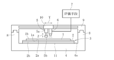
- the surface roughness evaluation apparatus includes a mounting table 4 on which a stacked body 3 in which a glass substrate 1 and a reference glass substrate 2 are stacked is mounted. .
- the stacked body 3 is placed on the placement surface 4 a of the placement table 4.
- the glass substrate 1 and the reference glass substrate 2 are rectangular in this embodiment, but may be circular, for example.
- the evaluation surface 1a for evaluating the surface roughness of the glass substrate 1 and the reference smooth surface 2a of the reference glass substrate 2 are in contact with each other.
- the evaluation surface 1 a of the glass substrate 1 constitutes the lower surface of the glass substrate 1
- the reference smooth surface 2 a of the reference glass substrate 2 constitutes the upper surface of the reference glass substrate 2.
- the surface roughening treatment method is not particularly limited, and examples thereof include chemical polishing such as etching, mechanical polishing such as tape polishing, brush polishing, and abrasive polishing, and chemical mechanical polishing (CMP).
- CMP chemical mechanical polishing
- only one surface (evaluation surface 1a) of the glass substrate 1 is roughened, and the other surface of the glass substrate 1 remains a smooth surface.
- the glass substrate 1 is formed by a known method such as an overflow method, a slot down draw method, a redraw method, or a float method.
- the reference smooth surface 2a of the reference glass substrate 2 has such a degree of smoothness that the interface is in close contact (for example, optical contact) when brought into contact with the reference smooth surface of another reference glass substrate manufactured under the same conditions. ing.
- the reference glass substrate 2 is formed by the overflow method, and the reference smooth surface 2a is an unpolished surface. That is, the reference smooth surface 2a is a fire-making surface.
- the surface roughness Ra of the reference smooth surface 2a is preferably 0.2 nm or less, more preferably 0.08 to 0.19 nm, and further preferably 0.16 to 0.18 nm. Ra is a value measured according to JIS B0601: 2001 (the same applies hereinafter).
- the surface (unpolished surface) formed by the float method or the float method is used. It may be a polished surface obtained by polishing the molded surface.
- the size of the reference glass substrate 2 may be the same as the size of the glass substrate 1, but may be larger or smaller than the size of the glass substrate 1.
- one side of the glass substrate 1 is preferably 100 to 3050 mm, more preferably 200 to 1000 mm, and one side of the reference glass substrate 2 is preferably 100 to 100 mm. It is 3500 mm, more preferably 200 to 1000 mm.
- the thickness of the reference glass substrate 2 may be the same as the thickness of the glass substrate 1, but may be larger or smaller than the thickness of the glass substrate 1.
- the thickness of the glass substrate 1 is preferably 0.1 to 2.0 mm, more preferably 0.2 to 1.5 mm, and the thickness of the reference glass substrate 2 is preferably 0.1 to 2.0 mm, More preferably, it is 0.2 to 1.1 mm.
- the mounting table 4 includes a pressing means 5 that locally presses the upper surface 1b of the glass substrate 1 (the upper surface of the laminate 3), an evaluation surface 1a of the glass substrate 1 that accompanies the pressing, and a reference smooth surface of the reference glass substrate 2.
- An imaging means 6 is provided for imaging a change mode of the close contact area with 2a (see FIGS. 3A and 3B).
- the imaging unit 6 is connected to an evaluation unit 7 that evaluates the surface roughness of the evaluation surface 1a of the glass substrate 1 based on a change mode of the imaged close contact area, wirelessly or by wire.
- the pressing means 5 includes a cylinder 5 a that can move forward and backward with respect to the upper surface 1 b of the glass substrate 1, and a pad 5 b that is provided at the tip of the cylinder 5 a and contacts the upper surface 1 b of the glass substrate 1.
- the pad 5b is formed of an elastic member such as rubber.
- the pressing force by the pad 5b is preferably 1 to 30N, and more preferably 5 to 15N.
- the pressing means 5 includes a pressure measuring unit that measures the pressing force of the pad 5b and a pressure control unit that controls the magnitude of the pressing force of the pad 5b.
- the imaging means 6 is composed of a small camera such as a CCD camera.
- a pair of first guide portions 8 are disposed on both sides of the mounting surface 4 a of the mounting table 4 in parallel with the side of the glass substrate 1. Between the pair of first guide portions 8, a second guide portion 9 is stretched so as to be orthogonal to the side of the glass substrate 1.
- the second guide portion 9 is movable along the pair of first guide portions 8 in the X direction parallel to the side of the glass substrate 1.
- the second guide portion 9 is provided with a support portion 10 that supports the pressing means 5 and the imaging means 6.
- the support part 10 is movable along the second guide part 9 in the Y direction orthogonal to the side of the glass substrate 1. Therefore, the pressing unit 5 and the imaging unit 6 are movable in a direction parallel to the side of the glass substrate 1 (X direction) and a direction orthogonal to the side of the glass substrate 1 (Y direction).
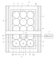
- an auxiliary sheet 11 on which a plurality of circles 11a are drawn is laid under the lower surface 2b of the reference glass substrate 2 (the lower surface of the laminate 3). Since the laminate 3 is transparent, each circle 11a of the auxiliary sheet 11 can be observed from above as shown in FIG.
- the plurality of circles 11 a are drawn in a region corresponding to substantially the entire surface of the glass substrate 1 of the laminate 3.
- Each circle 11a has the same radius, and a part of the circumference of adjacent circles 11a is in contact with each other.
- the radius of the circle 11a is not particularly limited, but is set to 100 mm in this embodiment.
- the circles 11a of the auxiliary sheet 11 may be separated from each other or may be overlapped. Further, the auxiliary sheet 11 may be laid on the upper surface 1 b of the glass substrate 1.
- the pad 5b of the pressing means 5 presses the upper surface 1b of the glass substrate 1 at a position corresponding to the center O of each circle 11a of the auxiliary sheet 11, and forms a pressing portion A where the pad 5b contacts the upper surface 1b of the glass substrate 1.
- the pad 5b is separated from the upper surface 1b of the glass substrate 1 once the upper surface 1b of the glass substrate 1 is pressed with the pressing force described above.
- the imaging means 6 images the change mode of the contact area in each circle 11a until a predetermined time elapses after the pad 5b presses the upper surface 1b of the glass substrate 1. Therefore, the imaging by the imaging unit 6 is performed even when the pad 5 b is separated from the upper surface 1 b of the glass substrate 1.
- the area of the pressing part A is preferably 0.1 to 20 cm 2 , more preferably 0.3 to 10 cm 2 .
- the evaluation means 7 measures the spread speed of the contact area in the radial direction from the image data captured by the imaging means 6 in each circle 11a as a change mode of the contact area.
- the spreading speed is measured by the time from when the upper surface 1b of the glass substrate 1 is pressed by the pad 5b until the outer edge of the adhesion area that spreads around the pressing portion A reaches the circumference of each circle 11a (see below). 3A and FIG. 3B).
- the mounting surface 4a of the mounting table 4 is a flat surface that is seamless.
- the mounting surface 4a may be formed of a hard material such as metal or resin (for example, an elastic modulus of 10,000 to 206000 MPa) or a soft material such as rubber (for example, an elastic modulus of 2 to 1000 MPa). Also good.
- a hard material such as metal or resin (for example, an elastic modulus of 10,000 to 206000 MPa) or a soft material such as rubber (for example, an elastic modulus of 2 to 1000 MPa).
- the flatness of the mounting surface 4a is good, and in the case of a soft material, there is an advantage that the glass is difficult to break when pressed.
- the mounting table 4 is provided with a positioning mechanism (for example, a positioning pin) for positioning the stacked body 3 on the mounting surface 4a.
- a positioning mechanism for example, a positioning pin
- the glass substrate is placed on the placed reference glass substrate 2. 1 is placed. That is, the laminated body 3 formed by stacking the reference glass substrate 2 and the glass substrate 1 is produced on the mounting surface 4a.
- standard glass substrate 2 is performed by the transfer apparatus not shown.
- the glass substrate 1 and the reference glass substrate 2 may be simultaneously placed on the placement table 4 in the state of the laminated body 3 in which the glass substrate 1 and the reference glass substrate 2 are stacked. In this case, the glass substrate 1, the reference glass substrate 2, and the auxiliary sheet 11 may be simultaneously placed on the placement table 4 in a state where the laminate 3 and the auxiliary sheet 11 are overlapped.
- the glass substrate 1 and the reference glass substrate 2 are preferably washed before being placed on the mounting table 4.
- Examples of the cleaning method include cleaning using an alkaline detergent, ionic water, or both.
- the contact angles of the evaluation surface 1a of the glass substrate 1 and the reference smooth surface 2a of the reference glass substrate 2 are preferably 1 to 50 °, more preferably 2 to 40 °.
- the pressing means 5 moves in the X direction and the Y direction with the pad 5b retracted upward from the upper surface 1b of the glass substrate 1.
- the pressing means 5 is sequentially positioned at a position corresponding to the center O of each circle 11 a in the plane of the glass substrate 1.
- the imaging unit 6 moves in the X direction and the Y direction together with the pressing unit 5, the change mode of the close contact region is also sequentially imaged at the position corresponding to each circle 11a.
- the positioned pressing means 5 extends the cylinder 5a downward (Z direction in FIG. 2) and presses the upper surface 1b of the glass substrate 1 with the pad 5b.
- a pressing portion A is formed at a position corresponding to the center O of the circle 11a.
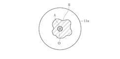
- the evaluation surface 1a of the glass substrate 1 and the reference smooth surface 2a of the reference glass substrate 2 are in close contact with each other, and an adhesion region B centering on the pressing portion A is formed.
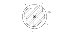
- This close contact region B gradually expands in the radial direction of the circle 11a as time passes after pressing, and changes from the state shown in FIG. 3A to the state shown in FIG.
- the pad 5b momentarily presses the upper surface 1b of the glass substrate 1 with a predetermined pressing force, and then moves away from the upper surface 1b of the glass substrate 1 by contraction of the cylinder 5a. Therefore, the imaging means 6 images the spread of the contact area B after the pad 5b is separated in addition to the spread of the contact area B when the pad 5b is pressed.
- the evaluation means 7 Based on the imaging data of the imaging means 6, the evaluation means 7 brings the pad 5 b into contact with the upper surface 1 b of the glass substrate 1, and then any part of the outer edge of the adhesion region B is first placed on the circumference of the circle 11 a. Measure the arrival time to reach.
- the point P is a portion of the outer edge of the contact area B that first reaches the circumference of the circle 11a.
- the evaluation means 7 when the measured arrival time (time to reach the point P) is 3 seconds or more (preferably 10 seconds or more), the surface roughness of the evaluation surface 1a of the glass substrate 1 is appropriate. It is judged that.
- the glass substrate 1 when the spreading speed in the radial direction of the adhesion region B is 0.03 m / s or less (preferably 0.01 m / s or less), it is determined that the glass substrate 1 is a non-defective product.
- the surface roughness of the evaluation surface 1a of the glass substrate 1 is very rough (for example, when the Ra of the evaluation surface 1a of the glass substrate 1 is 0.7 nm or more), the evaluation surface 1a of the glass substrate 1 and the reference glass
- the adhesion region B may not be formed at the interface of the reference smooth surface 2a of the substrate 2.
- the glass substrate 1 may be determined to be a non-defective product from the viewpoint of preventing the peeling charge of the glass substrate 1, but a defect such as a risk of breakage of the glass substrate 1 may be considered. Good.
- the laminate 3 is taken out from the mounting table 4 by a transfer device (not shown). In addition, you may take out the glass substrate 1 and the reference
- the spreading speed of the adhesion region B is slow when the surface roughness of the evaluation surface 1a of the glass substrate 1 is sufficiently rough, and is fast when the surface roughness of the evaluation surface 1a of the glass substrate 1 is not rough. Therefore, the spreading speed of the adhesion region B accurately reflects the surface roughness of the evaluation surface 1 a of the glass substrate 1.
- the inventors of the present application have found that the spreading speed of the adhesion region B is 0.03 m / s or less when the reference smooth surface 2a of the reference glass substrate 2 is an unpolished surface formed by the overflow method.
- the method for evaluating the surface roughness of the glass substrate 1 as described above is performed in the manufacturing process of the glass substrate 1. That is, a plurality of glass substrates 1 are formed by a known forming method such as an overflow method. One surface of the plurality of formed glass substrates 1 is roughened under the same conditions. One or a plurality of glass substrates 1 are selected from among them, and the surface roughness is evaluated by the above method. As a result, when the surface roughness of the roughened surface of the glass substrate 1 (corresponding to the evaluation surface 1a) is evaluated as appropriate (when the spreading speed of the adhesion region B is 0.03 m / s or less). Continues the production of the glass substrate 1 under the same conditions.
- the roughening of the glass substrate 1 is performed.
- the condition of the surface treatment is adjusted, and after the adjustment, the surface roughness of the surface subjected to the surface roughening treatment of the glass substrate 1 is similarly evaluated. This series of flows is repeated until it is determined that the surface roughness of the surface of the glass substrate 1 subjected to the roughening treatment is appropriate.
- the glass substrate 1 used for the evaluation of the surface roughness is discarded.
- the spreading speed of the adhesion region is 0.03 m / s or less. Become. For example, it is used as a glass substrate for FPD such as a liquid crystal display. In addition, when the roughened surface of the glass substrate is too rough, there is a demerit that the risk of breakage of the glass substrate increases or the time of the roughening treatment becomes longer than necessary.
- the spreading speed of the adhesion region of the glass substrate is preferably 0.0001 m / s or more, and more preferably 0.001 m / s or more.
- the inventors of the present application conducted a comparative test in order to verify the effectiveness of the present invention.
- the conditions of the comparative test are as follows.
- the surface roughness of the surface of each glass substrate subjected to the roughening treatment is as follows: (1) a method in which Ra value measured by a conventional AFM is 0.3 nm or more, and (2) an adhesion region of the present invention. Each of these was evaluated by two types of methods, ie, a method of making a non-defective product having a spreading speed in the radial direction of 0.03 m / s or less. Thereafter, the glass substrate whose surface roughness was evaluated by each method was passed through the actual manufacturing process of the liquid crystal display, and the charge amount was measured. If the charge amount is 1.7 kV or more, there is a risk of electrostatic breakdown.
- this invention is not limited to said embodiment, It can implement with a various form.
- the case where the pressing unit and the imaging unit are moved while the stacked body in which the glass substrate and the reference glass substrate are stacked is stationary has been described. Any body that moves relative to the body may be used.
- the stacked body may move while the pressing unit and the imaging unit are stationary.
- the upper surface of the laminate is mechanically pressed.
- the upper surface of the laminate may be pressed with a human finger or the like.
- the laminated body is manufactured with the glass substrate up and the reference glass substrate down has been described.
- the laminated body is prepared with the glass substrate down and the reference glass substrate up. It may be produced.
- the auxiliary sheet on which a plurality of circles are drawn has been described.
- the auxiliary sheet may be omitted.
- a plurality of circles may be drawn directly on the placement surface of the placement table, or a plurality of virtual circle data may be directly reflected in the image data captured by the imaging means.
- the change mode of the close contact region is measured by the spreading speed in the radial direction of the close contact region
- the change mode of the close contact region may be measured by the area of the close contact region.
- the area of the contact region is measured after a predetermined time has elapsed since the pressing (for example, after 3 seconds, preferably after 10 seconds).
Landscapes
- Chemical & Material Sciences (AREA)
- Engineering & Computer Science (AREA)
- Organic Chemistry (AREA)
- Materials Engineering (AREA)
- Geochemistry & Mineralogy (AREA)
- General Chemical & Material Sciences (AREA)
- Chemical Kinetics & Catalysis (AREA)
- Life Sciences & Earth Sciences (AREA)
- Physics & Mathematics (AREA)
- General Physics & Mathematics (AREA)
- Mechanical Engineering (AREA)
- Ceramic Engineering (AREA)
- Spectroscopy & Molecular Physics (AREA)
- Surface Treatment Of Glass (AREA)
- Length Measuring Devices By Optical Means (AREA)
Abstract
ガラス基板1の表面粗さを評価する評価面を、基準ガラス基板2の基準平滑面に接触させた状態で、ガラス基板1と基準ガラス基板2を重ねて積層体3を作製する。積層体3の上面を局所的に押圧し、押圧に伴うガラス基板1の評価面と基準ガラス基板2の基準平滑面との密着領域の変化態様に基づいて、ガラス基板1の評価面の表面粗さを評価する。密着領域の変化態様は、押圧部Aを中心とした密着領域の半径方向の広がり速度で測定する。
Description
本発明は、ガラス基板の表面粗さを評価するための技術に関する。
液晶ディスプレイや有機ELディスプレイなどのフラットパネルディスプレイ(FPD)には、ガラス基板が用いられている。ガラス基板には、FPDの製造工程の中で、半導体素子や電極などの種々の素子が形成される。
ガラス基板は、FPDの製造工程の中で、帯電しやすい環境下に置かれることが多い。例えば、FPDの製造工程に含まれる成膜などの工程では、金属又は絶縁体からなる載置テーブルの上にガラス基板を載置した状態で所定の処理が施され、処理後に載置テーブルからガラス基板が取り外される。この際、ガラス基板が載置テーブルに密着していると、剥離時にガラス基板に剥離帯電が生じ、静電気が蓄積される。このように帯電したガラス基板に導電性物質が近づくと放電が生じ、ガラス基板上の素子(電極線や半導体素子)が静電破壊する原因となる。なお、このような問題は、ガラス基板が無アルカリガラスで形成されている場合に特に顕著になる。
そこで、例えば、特許文献1には、剥離帯電を防止するために、ガラス基板において、素子が形成される第1の表面とは反対の第2の表面を粗面化処理し、表面凹凸を積極的に形成することが開示されている。同文献では、ガラス基板の第2の表面の表面粗さは、Raの値で管理されている。詳細には、ガラス基板の第2の表面のRaが0.3nm以上のときを良品としている。
しかしながら、ガラス基板の表面粗さをRaで管理した場合、次のような不具合が生じ得る。すなわち、Raの測定は、AFMなどを用いる必要があるので、ガラス基板表面の中の極めて小さな領域の評価しかできない。そのため、Raに基づいたガラス基板の表面粗さの評価が、ガラス基板全体の実際の表面粗さを正確に反映していない場合があり、剥離帯電を完全に防止できないという問題がある。
以上の実情に鑑み、本発明は、ガラス基板の表面粗さを正確に評価し、ガラス基板の剥離帯電を可及的に低減することを課題とする。
上記課題を解決するために創案された本発明は、ガラス基板の表面粗さ評価方法であって、ガラス基板の表面粗さを評価する評価面を、基準ガラス基板の基準平滑面に接触させた状態で、ガラス基板と前記基準ガラス基板を重ねて積層体を作製した後、積層体の少なくとも一方の表面を局所的に押圧し、押圧に伴うガラス基板の評価面と基準ガラス基板の基準平滑面との密着領域の変化態様に基づいて、ガラス基板の評価面の表面粗さを評価することを特徴とする。
このような構成によれば、ガラス基板の評価面の表面粗さが十分粗ければ、ガラス基板の評価面が、基準ガラス基板の基準平滑面に対して密着しにくい。そのため、積層体を局所的に押圧した際に、ガラス基板の評価面と基準ガラス基板の基準平滑面との間に密着領域が形成されないか、或いは、密着領域が形成されたとしても密着領域の広がりが非常に遅い。これに対し、ガラス基板の評価面の表面粗さが粗くなければ、ガラス基板の評価面が、基準ガラス基板の基準平滑面に対して密着しやすい。そのため、積層体を局所的に押圧した際に、ガラス基板の評価面と基準ガラス基板の基準平滑面との間に形成される密着領域の広がりが非常に速い。したがって、密着領域の変化態様は、ガラス基板の評価面の表面粗さを正確に反映する。また、押圧する箇所を変えることで、ガラス基板の評価面の広い範囲において、密着領域の変化態様を簡単に測定することができる。よって、密着領域の変化態様に基づいてガラス基板の表面粗さを評価すれば、ガラス基板の評価面の広い範囲の表面粗さを適正に評価でき、ガラス基板の剥離帯電を可及的に低減することができる。
上記の構成において、ガラス基板の評価面が、粗面化処理されていてもよい。
すなわち、ガラス基板の評価面は、積極的に表面凹凸が形成された面であってもよい。この場合、ガラス基板の評価面の表面粗さが不適当と評価されたとき、粗面化処理の条件を調整し直すことが好ましい。
上記の構成において、密着領域の変化態様を、押圧した箇所を中心とした密着領域の半径方向の広がり速度で測定してもよい。
このようにすれば、密着領域の変化態様を、広がり速度によって簡単かつ確実に把握することができる。
上記の構成において、基準ガラス基板が、オーバーフロー法によって成形されるとともに、基準ガラス基板の基準平滑面が未研磨であり、密着領域の広がり速度が0.3m/s以下である場合に、ガラス基板の評価面の表面粗さを適正と評価することが好ましい。
すなわち、本願発明者等は、鋭意実験を重ねた結果、基準ガラス基板の基準平滑面が、オーバーフロー法によって成形された未研磨面である場合に、密着領域の広がり速度が0.3m/s以下であると、ガラス基板の剥離帯電を確実に低減できることを知見するに至った。したがって、上記の構成に規定する条件を満足する場合に、ガラス基板の評価面の表面粗さを適正と評価することが好ましい。
上記の構成において、押圧時の押圧力が、1~30Nであることが好ましい。
このようにすれば、ガラス基板の評価面と基準ガラス基板の基準平滑面に適度な力が加わり、両者の密着領域の変化態様を測定しやすくなる。
上記課題を解決するために創案された本発明は、ガラス基板の表面粗さ評価装置であって、ガラス基板の表面粗さを評価する評価面を、基準ガラス基板の基準平滑面に接触させた状態で、ガラス基板と基準ガラス基板を重ねた積層体の表裏面のうち、少なくとも一方の面を局所的に押圧する押圧手段と、押圧に伴うガラス基板の評価面と基準ガラス基板の基準平滑面との密着領域の変化態様を撮像する撮像手段と、撮像された密着領域の変化態様に基づいて、ガラス基板の評価面の表面粗さを評価する評価手段とを備えていることを特徴とする。
このような構成によれば、既に述べた対応する構成と同様の作用効果を享受することができる。
上記の構成において、評価手段が、密着領域の変化態様として、押圧した箇所を中心とした密着領域の半径方向の広がり速度を測定することが好ましい。
この場合、基準ガラス基板が、オーバーフロー法によって成形されるとともに、基準ガラス基板の基準平滑面が未研磨であり、評価手段は、広がり速度が0.03m/s以下である場合に、ガラス基板の評価面の表面粗さを適正と評価することが好ましい。
上記課題を解決するために創案された本発明は、少なくとも一方の表面が粗面化処理されたガラス基板であって、ガラス基板の粗面化処理された面を評価面として、ガラス基板の評価面を、オーバーフロー法によって成形された基準ガラス基板の未研磨の基準平滑面に接触させた状態で、ガラス基板と基準ガラス基板を重ねて積層体を作製するとともに、積層体の一方の表面を局所的に押圧した場合に、押圧に伴うガラス基板の評価面と基準ガラス基板の基準平滑面との密着領域の広がり速度が、押圧した箇所を中心とする半径方向において、0.03m/s以下となることを特徴とする。
このような構成によれば、ガラス基板の粗面化処理された面の表面粗さが、適正な粗さとなり、剥離帯電を可及的に低減することができる。
以上のように本発明によれば、ガラス基板の表面粗さを正確に評価し、ガラス基板の剥離帯電を可及的に低減することができる。
以下、本発明の実施形態を添付図面を参照して説明する。
図1及び図2に示すように、本発明の実施形態に係る表面粗さ評価装置は、ガラス基板1と基準ガラス基板2を重ねた積層体3を載置する載置テーブル4を備えている。積層体3は、載置テーブル4の載置面4aに載置される。なお、ガラス基板1と基準ガラス基板2は、この実施形態では矩形状であるが、例えば円形などであってもよい。
積層体3の状態で、ガラス基板1の表面粗さを評価する評価面1aと、基準ガラス基板2の基準平滑面2aとが、互いに接触している。なお、この実施形態では、ガラス基板1の評価面1aはガラス基板1の下面を構成し、基準ガラス基板2の基準平滑面2aは基準ガラス基板2の上面を構成している。
ガラス基板1の評価面1aには、予め粗面化処理によって表面凹凸が形成されている。粗面化処理の方法は、特に限定されるものではないが、エッチングなどの化学研磨、テープ研磨・ブラシ研磨・砥粒研磨などの機械研磨、化学機械研磨(CMP)などが挙げられる。この実施形態では、ガラス基板1の一方の面(評価面1a)のみに粗面化処理が施されており、ガラス基板1の他方の面は平滑面のままである。ガラス基板1は、例えば、オーバーフロー法、スロットダウンドロー法、リドロー法、フロート法などの公知の方法で成形される。
基準ガラス基板2の基準平滑面2aは、同一条件で製造された別の基準ガラス基板の基準平滑面と接触させた場合に、界面が密着(例えば、オプティカルコンタクト)する程度の平滑度を有している。詳細には、基準ガラス基板2は、オーバーフロー法により成形されており、その基準平滑面2aは未研磨面である。すなわち、基準平滑面2aは火造り面である。基準平滑面2aの表面粗さRaは、0.2nm以下であることが好ましく、0.08~0.19nmであることがより好ましく、0.16~0.18nmであることが更に好ましい。Raは、JIS B0601:2001に準拠して測定した値とする(以下、同様)。なお、基準ガラス基板2の基準平滑面2aは、オーバーフロー法により成形された未研磨面と同程度の平滑度を有する場合には、フロート法により成形された面(未研磨面)又はフロート法により成形された面を研磨した研磨面であってもよい。
基準ガラス基板2のサイズは、ガラス基板1のサイズと同じであってもよいが、ガラス基板1のサイズよりも大きくてもよいし、小さくてもよい。例えば、ガラス基板1と基準ガラス基板2が矩形である場合、ガラス基板1の一辺は、好ましくは100~3050mm、更に好ましくは200~1000mmであり、基準ガラス基板2の一辺は、好ましくは100~3500mm、更に好ましくは200~1000mmである。
基準ガラス基板2の厚みは、ガラス基板1の厚みと同じであってもよいが、ガラス基板1の厚みよりも大きくてもよいし、小さくてもよい。例えば、ガラス基板1の厚みは、好ましくは0.1~2.0mm、更に好ましくは0.2~1.5mmであり、基準ガラス基板2の厚みは、好ましくは0.1~2.0mm、更に好ましくは0.2~1.1mmである。
載置テーブル4には、ガラス基板1の上面1b(積層体3の上面)を局所的に押圧する押圧手段5と、押圧に伴うガラス基板1の評価面1aと基準ガラス基板2の基準平滑面2aとの密着領域(図3A及び図3Bを参照)の変化態様を撮像する撮像手段6とが設けられている。また、撮像手段6には、撮像された密着領域の変化態様に基づいてガラス基板1の評価面1aの表面粗さを評価する評価手段7が無線又は有線で接続されている。
押圧手段5は、ガラス基板1の上面1bに対して進退移動可能なシリンダ5aと、シリンダ5aの先端に設けられ、ガラス基板1の上面1bに当接するパット5bとを備えている。パット5bはゴムなどの弾性部材で形成される。
パット5bによる押圧力は、1~30Nであることが好ましく、5~15Nであることがより好ましい。なお、押圧手段5は、図示は省略するが、パット5bの押圧力を測定する圧力測定部と、パット5bの押圧力の大きさを制御する圧力制御部とを備えている。
撮像手段6は、CCDカメラなどの小型カメラで構成されている。
載置テーブル4の載置面4aの両側方には、ガラス基板1の側辺と平行に一対の第1ガイド部8が配置されている。一対の第1ガイド部8の間には、ガラス基板1の側辺と直交するように第2ガイド部9が掛け渡されている。第2ガイド部9は、一対の第1ガイド部8に沿って、ガラス基板1の側辺と平行なX方向に移動可能となっている。第2ガイド部9には、押圧手段5及び撮像手段6を支持する支持部10が設けられている。支持部10は、第2ガイド部9に沿って、ガラス基板1の側辺と直交するY方向に移動可能となっている。したがって、押圧手段5及び撮像手段6は、ガラス基板1の側辺と平行な方向(X方向)、及びガラス基板1の側辺と直交する方向(Y方向)にそれぞれ移動可能となっている。
この実施形態では、基準ガラス基板2の下面2b(積層体3の下面)の下に、複数の円11aが描かれた補助シート11が敷設されている。積層体3は透明であるため、図1に示すように、上方から補助シート11の各円11aを観察できる。複数の円11aは、積層体3のガラス基板1の略全面に対応する領域に描かれている。各円11aは半径が同一であって、隣接する円11a同士の円周の一部が互いに接している。円11aの半径は、特に限定されるものではないが、この実施形態では100mmに設定されている。なお、補助シート11の円11aは、互いに離間していてもよいし、重複していてもよい。また、補助シート11は、ガラス基板1の上面1bの上に敷設されていてもよい。
押圧手段5のパット5bは、補助シート11の各円11aの中心Oに対応する位置でガラス基板1の上面1bを押圧し、ガラス基板1の上面1bにパット5bが接触する押圧部Aを形成する。パット5bは、上述の押圧力でガラス基板1の上面1bを一旦押圧したら、ガラス基板1の上面1bから離反する。撮像手段6は、パット5bがガラス基板1の上面1bを押圧してから所定時間が経過するまでの間、各円11aにおける密着領域の変化態様を撮像する。そのため、撮像手段6による撮像は、パット5bがガラス基板1の上面1bから離反した状態でも行われる。押圧部Aの面積は、好ましくは0.1~20cm2であり、更に好ましくは0.3~10cm2である。
評価手段7は、密着領域の変化態様として、各円11aにおいて、撮像手段6で撮像された撮影データから密着領域の半径方向の広がり速度を測定する。広がり速度は、パット5bでガラス基板1の上面1bを押圧してから、押圧部Aを中心として広がる密着領域の外縁が各円11aの円周に到達するまでの時間により測定する(後述する図3A及び図3Bを参照)。
なお、載置テーブル4の載置面4aは、継ぎ目なく連続した平面である。載置面4aは、金属や樹脂などの硬い材質(例えば弾性率が10000~206000MPa)で形成されていてもよいし、ゴムなどの柔らかい材質(例えば弾性率が2~1000MPa)で形成されていてもよい。硬い材質の場合、載置面4aの平面度が良好となり、柔らかい材質の場合、押圧時にガラスが割れにくくなるという利点がある。
また、載置テーブル4には、図示は省略するが、載置面4a上で積層体3を位置決めするための位置決め機構(例えば、位置決めピンなど)が設けられている。
次に、上記のように構成された表面粗さ評価装置によるガラス基板の表面粗さ評価方法を説明する。
まず、図1及び図2に示すように、載置テーブル4の補助シート11が敷設された載置面4aに基準ガラス基板2を載置した後、載置された基準ガラス基板2にガラス基板1を載置する。すなわち、基準ガラス基板2とガラス基板1を重ねてなる積層体3が、載置面4a上で作製される。なお、ガラス基板1及び基準ガラス基板2の載置作業は、不図示の移載装置によって行う。また、ガラス基板1と基準ガラス基板2を重ねた積層体3の状態で、載置テーブル4上にガラス基板1と基準ガラス基板2を同時に載置してもよい。この場合、積層体3と補助シート11を重ねた状態で、ガラス基板1、基準ガラス基板2及び補助シート11を同時に載置テーブル4上に載置してもよい。
ガラス基板1及び基準ガラス基板2は、載置テーブル4に配置する前に洗浄することが好ましい。洗浄方法としては、例えばアルカリ洗剤、イオン水、又はその両方を用いた洗浄が挙げられる。ガラス基板1の評価面1a及び基準ガラス基板2の基準平滑面2aのそれぞれの接触角は、好ましくは1~50°、更に好ましくは2~40°である。
次に、押圧手段5は、パット5bをガラス基板1の上面1bから上方に退避させた状態で、X方向及びY方向に移動する。この移動により、押圧手段5は、ガラス基板1の面内における各円11aの中心Oに対応する位置に順次位置決めされる。この際、押圧手段5と一緒に撮像手段6もX方向及びY方向に移動するため、各円11aに対応する位置で密着領域の変化態様も順次撮像される。
位置決めされた押圧手段5は、シリンダ5aを下方(図2のZ方向)に伸ばし、パット5bでガラス基板1の上面1bを押圧する。パット5bでガラス基板1の上面1bを押圧すると、円11aの中心Oに対応する位置に押圧部Aが形成される。そうすると、図3A及び図3Bに例示するように、ガラス基板1の評価面1aと基準ガラス基板2の基準平滑面2aが互いに密着し、押圧部Aを中心とする密着領域Bが形成される。この密着領域Bは、押圧してから時間が経過するに連れて円11aの半径方向に徐々に広がり、例えば、図3Aに示す状態から図3Bに示す状態に変化する。なお、パット5bは、ガラス基板1の上面1bを所定の押圧力で瞬間的に押圧した後、シリンダ5aの収縮によってガラス基板1の上面1bから離間する。そのため、撮像手段6は、パット5bを押圧したときの密着領域Bの広がりに加え、パット5bが離間した後の密着領域Bの広がりも撮像する。
評価手段7は、撮像手段6の撮像データに基づいて、パット5bをガラス基板1の上面1bに接触させてから、密着領域Bの外縁のいずれかの部分が、最初に円11aの円周に到達するまでの到達時間を測定する。図3Bでは、P地点が、密着領域Bの外縁のうち、最初に円11aの円周に到達した部分である。評価手段7は、測定された到達時間(P地点に到達するまでの時間)が、3秒以上(好ましくは10秒以上)である場合を、ガラス基板1の評価面1aの表面粗さが適正であると判断する。換言すれば、密着領域Bの半径方向の広がり速度が、0.03m/s以下(好ましくは0.01m/s以下)の場合に、ガラス基板1が良品であると判断する。ここで、ガラス基板1の評価面1aの表面粗さが非常に粗い場合(例えば、ガラス基板1の評価面1aのRaが0.7nm以上の場合)、ガラス基板1の評価面1aと基準ガラス基板2の基準平滑面2aの界面に密着領域Bが形成されないことがある。この場合、ガラス基板1の剥離帯電を防止する観点からはガラス基板1を良品と判断してもよいが、ガラス基板1の破損のリスクなどの不具合も考えられるため、不良品と判断してもよい。
そして、ガラス基板1の面内に形成された全ての円11aで表面粗さの評価が終了した後は、不図示の移載装置で、載置テーブル4から積層体3を取り出す。なお、ガラス基板1と基準ガラス基板2を別々に取り出してもよい。
上記のような表面粗さの評価方法によれば、次のような作用効果を享受し得る。すなわち、密着領域Bの広がり速度は、ガラス基板1の評価面1aの表面粗さが十分粗ければ遅くなり、ガラス基板1の評価面1aの表面粗さが粗くなければ速くなる。そのため、密着領域Bの広がり速度は、ガラス基板1の評価面1aの表面粗さを正確に反映する。本願発明者等は、鋭意研究を重ねた結果、基準ガラス基板2の基準平滑面2aがオーバーフロー法によって成形された未研磨面である場合に、密着領域Bの広がり速度が0.03m/s以下であれば、ガラス基板1の剥離帯電を確実に低減することができることを知見するに至った。そして、押圧部Aの形成位置を変化させることで、ガラス基板1の評価面1aの略全範囲に亘って、密着領域Bの広がり速度を簡単に測定することができる。したがって、上記のような表面粗さの評価方法によれば、ガラス基板1の評価面1aの略全範囲の表面粗さを適正に評価でき、ガラス基板1の剥離帯電を可及的に低減することができる。
ここで、上記のようなガラス基板1の表面粗さの評価方法は、ガラス基板1の製造工程の中で行われる。すなわち、複数枚のガラス基板1をオーバーフロー法などの公知の成形方法で成形する。成形された複数枚のガラス基板1の一方の面を同一条件で粗面化処理する。その中から任意の一枚又は複数枚のガラス基板1を選択し、上記の方法で表面粗さを評価する。その結果、ガラス基板1の粗面化処理された面(評価面1aに相当)の表面粗さが適正と評価された場合(密着領域Bの広がり速度が0.03m/s以下の場合)には、同一条件でガラス基板1の製造を継続する。一方、ガラス基板1の粗面化処理された面の表面粗さが不適正と評価された場合(密着領域Bの広がり速度が0.03m/s超の場合)には、ガラス基板1の粗面化処理の条件を調整し、調整後にガラス基板1の粗面化処理された面の表面粗さを同様に評価する。この一連の流れをガラス基板1の粗面化処理された面の表面粗さが適正と判断されるまで繰り返す。なお、表面粗さの評価に用いたガラス基板1は廃棄される。
このようにして製造されたガラス基板(表面粗さの評価に用いられたガラス基板を除く)は、表面粗さの評価を行った場合、密着領域の広がり速度が、0.03m/s以下になる。そして、例えば、液晶ディスプレイなどのFPD用のガラス基板として用いられる。なお、ガラス基板の粗面化処理された面が粗すぎると、ガラス基板の破損のリスクが高まったり、粗面化処理の時間が必要以上に長くなったりするというデメリットがあるため、製造されたガラス基板の密着領域の広がり速度は、0.0001m/s以上であることが好ましく、0.001m/s以上であることがより好ましい。
本願発明者等は、本願発明の有効性を検証するために、比較試験を行った。比較試験の条件は、次の通りである。
まず、表面粗さを評価するガラス基板を10枚用意した。次に、このガラス基板の一方の表面にエッチングにより粗面化処理を施した。各ガラス基板の粗面化処理された面の表面粗さを、(1)従来のAFMによって測定されたRaの値が0.3nm以上を良品とする方法と、(2)本願発明の密着領域の半径方向の広がり速度が0.03m/s以下を良品とする方法の2種類の方法でそれぞれ評価した。その後、それぞれの方法で表面粗さが評価されたガラス基板を実際の液晶ディスプレイの製造工程に流し、帯電量を測定した。なお、帯電量は1.7kV以上であれば静電破壊のリスクがある。
比較試験の結果、上記(1)の従来の方法では、良品とされたガラス基板のうち、30%のガラス基板において帯電量が1.7kV以上となり、静電破壊のリスクのあるガラス基板が見逃されるに至った。これに対し、上記(2)の本願発明の方法では、良品とされたガラス基板の中に、帯電量が1.7kV以上となるものはなかった。このことからも、本願発明の評価方法を用いれば、ガラス基板の剥離帯電を可及的に低減し、ガラス基板に形成される素子の静電破壊を有効に防止できることが分かる。
なお、本発明は、上記の実施形態に限定されるものではなく、種々の形態で実施することができる。
例えば、上記の実施形態では、押圧手段と撮像手段を一組設けた場合を説明したが、押圧手段と撮像手段は複数組設けられていてもよい。
また、上記の実施形態では、ガラス基板と基準ガラス基板を重ねた積層体を静止させた状態で、押圧手段と撮像手段を移動させる場合を説明したが、押圧手段と撮像手段に対して、積層体が相対移動するものであればよい。例えば、押圧手段と撮像手段を静止させた状態で、積層体が移動するものであってもよい。
また、上記の実施形態では、積層体の上面を機械的に押圧する場合を説明したが、積層体の上面を人の手指などで押圧してもよい。
また、上記の実施形態では、積層体の上面のみを押圧する場合を説明したが、積層体の下面のみを押圧するようにしてもよいし、積層体の上面と下面の対応する位置を上下両側から押圧するようにしてもよい。
また、上記の実施形態では、ガラス基板を上、基準ガラス基板を下とした状態で積層体を作製する場合を説明したが、ガラス基板を下、基準ガラス基板を上とした状態で積層体を作製してもよい。
また、上記の実施形態では、複数の円が描かれた補助シートを用いる場合を説明したが、補助シートは省略してもよい。この場合、例えば、複数の円を載置テーブルの載置面に直接描いてもよいし、撮像手段で撮像された撮像データに複数の仮想円データを直接反映させてもよい。
また、上記の実施形態では、密着領域の変化態様を密着領域の半径方向の広がり速度で測定する場合を説明したが、密着領域の変化態様を密着領域の面積で測定してもよい。この場合、密着領域の面積は、押圧してから所定時間経過後(例えば3秒後、好ましくは10秒後)に測定する。
1 ガラス基板
1a 評価面
2 基準ガラス基板
2a 基準平滑面
3 積層体
4 載置テーブル
4a 載置面
5 押圧手段
5a シリンダ
5b パット
6 撮像手段
7 評価手段
8 第1ガイド部
9 第2ガイド部
10 支持部
11 補助シート
11a 円
A 押圧部
B 密着領域
1a 評価面
2 基準ガラス基板
2a 基準平滑面
3 積層体
4 載置テーブル
4a 載置面
5 押圧手段
5a シリンダ
5b パット
6 撮像手段
7 評価手段
8 第1ガイド部
9 第2ガイド部
10 支持部
11 補助シート
11a 円
A 押圧部
B 密着領域
Claims (9)
- ガラス基板の表面粗さ評価方法であって、
前記ガラス基板の表面粗さを評価する評価面を、基準ガラス基板の基準平滑面に接触させた状態で、前記ガラス基板と前記基準ガラス基板を重ねて積層体を作製した後、
前記積層体の少なくとも一方の表面を局所的に押圧し、
前記押圧に伴う前記ガラス基板の評価面と前記基準ガラス基板の基準平滑面との密着領域の変化態様に基づいて、前記ガラス基板の評価面の表面粗さを評価することを特徴とする表面粗さ評価方法。 - 前記ガラス基板の評価面が、粗面化処理されていることを特徴とする請求項1に記載の表面粗さ評価方法。
- 前記密着領域の変化態様を、前記押圧した箇所を中心とした前記密着領域の半径方向の広がり速度で測定することを特徴とする請求項1又は2に記載の表面粗さ評価方法。
- 前記基準ガラス基板が、オーバーフロー法によって成形されるとともに、前記基準ガラス基板の基準平滑面が未研磨であり、
前記密着領域の広がり速度が0.03m/s以下である場合に、前記ガラス基板の評価面の表面粗さを適正と評価することを特徴とする請求項3に記載の表面粗さ評価方法。 - 前記押圧時の押圧力が、1~30Nであることを特徴とする請求項1~4のいずれか1項に記載の表面粗さ評価方法。
- ガラス基板の表面粗さ評価装置であって、
前記ガラス基板の表面粗さを評価する評価面を、基準ガラス基板の基準平滑面に接触させた状態で、前記ガラス基板と前記基準ガラス基板を重ねた積層体の少なくとも一方の表面を局所的に押圧する押圧手段と、
前記押圧に伴う前記ガラス基板の評価面と前記基準ガラス基板の基準平滑面との密着領域の変化態様を撮像する撮像手段と、
前記撮像された密着領域の変化態様に基づいて、前記ガラス基板の評価面の表面粗さを評価する評価手段とを備えていることを特徴とする表面粗さ評価装置。 - 前記評価手段が、前記密着領域の変化態様として、前記押圧した箇所を中心とした前記密着領域の半径方向の広がり速度を測定することを特徴とする請求項6に記載の表面粗さ評価装置。
- 前記基準ガラス基板が、オーバーフロー法によって成形されるとともに、前記基準ガラス基板の基準平滑面が未研磨であり、
前記評価手段は、前記広がり速度が0.03m/s以下である場合に、前記ガラス基板の評価面の表面粗さを適正と評価することを特徴とする請求項7に記載の表面粗さ評価装置。 - 少なくとも一方の表面が粗面化処理されたガラス基板であって、
前記ガラス基板の前記粗面化処理された面を評価面として、前記ガラス基板の評価面を、オーバーフロー法によって成形された基準ガラス基板の未研磨の基準平滑面に接触させた状態で、前記ガラス基板と前記基準ガラス基板を重ねて積層体を作製するとともに、前記積層体の一方の表面を局所的に押圧した場合に、
前記押圧に伴う前記ガラス基板の評価面と前記基準ガラス基板の基準平滑面との密着領域の広がり速度が、前記押圧した箇所を中心とする半径方向において、0.03m/s以下となることを特徴とするガラス基板。
Priority Applications (2)
| Application Number | Priority Date | Filing Date | Title |
|---|---|---|---|
| CN201680027249.9A CN107532877B (zh) | 2015-05-25 | 2016-05-12 | 表面粗糙度评价方法、表面粗糙度评价装置以及玻璃基板 |
| KR1020177025389A KR102576955B1 (ko) | 2015-05-25 | 2016-05-12 | 표면 조도 평가 방법, 표면 조도 평가 장치 및 유리 기판 |
Applications Claiming Priority (2)
| Application Number | Priority Date | Filing Date | Title |
|---|---|---|---|
| JP2015-105483 | 2015-05-25 | ||
| JP2015105483A JP6531940B2 (ja) | 2015-05-25 | 2015-05-25 | 表面粗さ評価方法、表面粗さ評価装置およびガラス基板 |
Publications (1)
| Publication Number | Publication Date |
|---|---|
| WO2016190117A1 true WO2016190117A1 (ja) | 2016-12-01 |
Family
ID=57392722
Family Applications (1)
| Application Number | Title | Priority Date | Filing Date |
|---|---|---|---|
| PCT/JP2016/064092 Ceased WO2016190117A1 (ja) | 2015-05-25 | 2016-05-12 | 表面粗さ評価方法、表面粗さ評価装置およびガラス基板 |
Country Status (4)
| Country | Link |
|---|---|
| JP (1) | JP6531940B2 (ja) |
| KR (1) | KR102576955B1 (ja) |
| CN (1) | CN107532877B (ja) |
| WO (1) | WO2016190117A1 (ja) |
Families Citing this family (3)
| Publication number | Priority date | Publication date | Assignee | Title |
|---|---|---|---|---|
| CN107621219A (zh) * | 2017-09-04 | 2018-01-23 | 成都随如科技有限公司 | 用于镜面检测的轮廓仪 |
| CN111055223B (zh) * | 2019-12-26 | 2021-10-01 | 苏州肯美威机械制造有限公司 | 一种机加工零件光学检验用辅助定位工装 |
| KR20250099991A (ko) * | 2023-12-26 | 2025-07-03 | 오씨아이 주식회사 | 연속식 기판가공장치 및 이를 사용한 연속식 기판가공방법 |
Citations (4)
| Publication number | Priority date | Publication date | Assignee | Title |
|---|---|---|---|---|
| JPH0843062A (ja) * | 1994-07-29 | 1996-02-16 | Sony Corp | 表面粗さ検出装置及び表面粗さ検出方法 |
| JP2006138754A (ja) * | 2004-11-12 | 2006-06-01 | Hitachi High-Tech Electronics Engineering Co Ltd | ディスク表面検査方法及びその装置 |
| JP2009036523A (ja) * | 2007-07-31 | 2009-02-19 | Lasertec Corp | 粗さ測定方法及び粗さ測定装置 |
| WO2010128673A1 (ja) * | 2009-05-07 | 2010-11-11 | 日本電気硝子株式会社 | ガラス基板及びその製造方法 |
Family Cites Families (8)
| Publication number | Priority date | Publication date | Assignee | Title |
|---|---|---|---|---|
| JP5169194B2 (ja) * | 2006-12-14 | 2013-03-27 | 日本電気硝子株式会社 | 板ガラス欠陥検出装置、板ガラスの製造方法 |
| JP2010527891A (ja) * | 2007-05-18 | 2010-08-19 | コーニング インコーポレイテッド | ガラス製造プロセスにおける含有物を最小化する方法及び装置 |
| KR20090055081A (ko) * | 2007-11-28 | 2009-06-02 | 삼성중공업 주식회사 | 표면조도를 이용한 비접촉식 도막 측정장치 및 그의 방법 |
| US7810355B2 (en) * | 2008-06-30 | 2010-10-12 | Apple Inc. | Full perimeter chemical strengthening of substrates |
| FR2934588B1 (fr) * | 2008-07-30 | 2011-07-22 | Fives Stein | Procede et dispositif de realisation d'une structure sur l'une des faces d'un ruban de verre |
| CN102446673A (zh) * | 2010-09-30 | 2012-05-09 | 旭硝子株式会社 | 显示器用玻璃基板及其制造方法 |
| KR101269128B1 (ko) * | 2011-06-29 | 2013-05-29 | 국립대학법인 울산과학기술대학교 산학협력단 | 중간시점 영상 생성기를 갖는 표면 거칠기 측정 장치 및 방법 |
| KR101517726B1 (ko) * | 2014-03-12 | 2015-05-04 | 노바테크인더스트리 주식회사 | 에칭용 지그 |
-
2015
- 2015-05-25 JP JP2015105483A patent/JP6531940B2/ja active Active
-
2016
- 2016-05-12 KR KR1020177025389A patent/KR102576955B1/ko active Active
- 2016-05-12 WO PCT/JP2016/064092 patent/WO2016190117A1/ja not_active Ceased
- 2016-05-12 CN CN201680027249.9A patent/CN107532877B/zh active Active
Patent Citations (4)
| Publication number | Priority date | Publication date | Assignee | Title |
|---|---|---|---|---|
| JPH0843062A (ja) * | 1994-07-29 | 1996-02-16 | Sony Corp | 表面粗さ検出装置及び表面粗さ検出方法 |
| JP2006138754A (ja) * | 2004-11-12 | 2006-06-01 | Hitachi High-Tech Electronics Engineering Co Ltd | ディスク表面検査方法及びその装置 |
| JP2009036523A (ja) * | 2007-07-31 | 2009-02-19 | Lasertec Corp | 粗さ測定方法及び粗さ測定装置 |
| WO2010128673A1 (ja) * | 2009-05-07 | 2010-11-11 | 日本電気硝子株式会社 | ガラス基板及びその製造方法 |
Also Published As
| Publication number | Publication date |
|---|---|
| JP6531940B2 (ja) | 2019-06-19 |
| JP2016217973A (ja) | 2016-12-22 |
| CN107532877A (zh) | 2018-01-02 |
| KR20180011052A (ko) | 2018-01-31 |
| KR102576955B1 (ko) | 2023-09-11 |
| CN107532877B (zh) | 2020-02-14 |
Similar Documents
| Publication | Publication Date | Title |
|---|---|---|
| JP5949894B2 (ja) | ガラス積層体及びその製造方法、並びに表示パネルの製造方法及びその製造方法により得られる表示パネル | |
| TWI585028B (zh) | 剝離裝置及剝離方法 | |
| JP6312270B2 (ja) | デバイスチップを用いた電子デバイスの製造方法およびその製造装置 | |
| US8454851B2 (en) | Manufacturing method of the flexible display device | |
| KR20160146699A (ko) | 적층체의 기판 분리 장치 | |
| WO2016177286A1 (zh) | 一种压膜装置及压膜方法 | |
| CN107688403A (zh) | 曲面贴合装置及贴合方法 | |
| KR20170084412A (ko) | 디스플레이 장치 및 그 제조방법 | |
| CN102802817A (zh) | 超声波接合用工具、超声波接合用工具的制造方法、超声波接合方法及超声波接合装置 | |
| JP6397667B2 (ja) | 貼合装置、貼合方法、光学表示デバイスの生産システムおよび光学表示デバイスの生産方法 | |
| JP6531940B2 (ja) | 表面粗さ評価方法、表面粗さ評価装置およびガラス基板 | |
| KR102638010B1 (ko) | 마이크로 LED 디스플레이의 칩 리페어를 위한 픽앤플레이스(Pick-and-Place) 장치 | |
| JP6032428B2 (ja) | ガラスフィルム切断装置及びガラスフィルム切断方法 | |
| KR102172312B1 (ko) | 접합 장치, 접합 방법, 광학 표시 디바이스의 생산 시스템 및 광학 표시 디바이스의 생산 방법 | |
| JP2013095006A (ja) | 貼付装置および貼付方法 | |
| KR101397094B1 (ko) | 라미네이팅 장치 및 라미네이팅 방법 | |
| KR101545192B1 (ko) | 선단기포 제거기능을 갖는 필름 부착장치 | |
| JP2015034731A (ja) | 試験装置、試験方法 | |
| JP2011016202A (ja) | 異物研磨装置 | |
| JP7811341B2 (ja) | 板ガラスの製造方法、その製造装置及び板ガラス | |
| JPH086027A (ja) | 配向膜に対する凹凸模様の転写装置 | |
| CN102639295B (zh) | 工件表面的异物研磨方法和异物研磨装置 | |
| TWM647866U (zh) | 晶圓膠膜移除裝置 | |
| CN102496600B (zh) | 可挠式显示面板的制造方法 | |
| KR102026441B1 (ko) | 정전척 세정이 가능한 라미네이팅 장치 및 이의 세정 방법 |
Legal Events
| Date | Code | Title | Description |
|---|---|---|---|
| 121 | Ep: the epo has been informed by wipo that ep was designated in this application |
Ref document number: 16799825 Country of ref document: EP Kind code of ref document: A1 |
|
| ENP | Entry into the national phase |
Ref document number: 20177025389 Country of ref document: KR Kind code of ref document: A |
|
| NENP | Non-entry into the national phase |
Ref country code: DE |
|
| 122 | Ep: pct application non-entry in european phase |
Ref document number: 16799825 Country of ref document: EP Kind code of ref document: A1 |