WO2016181958A1 - 電子デバイスおよびその製造方法 - Google Patents
電子デバイスおよびその製造方法 Download PDFInfo
- Publication number
- WO2016181958A1 WO2016181958A1 PCT/JP2016/063841 JP2016063841W WO2016181958A1 WO 2016181958 A1 WO2016181958 A1 WO 2016181958A1 JP 2016063841 W JP2016063841 W JP 2016063841W WO 2016181958 A1 WO2016181958 A1 WO 2016181958A1
- Authority
- WO
- WIPO (PCT)
- Prior art keywords
- polymer nanosheet
- electronic device
- nanosheet
- polymer
- conductive wiring
- Prior art date
- Legal status (The legal status is an assumption and is not a legal conclusion. Google has not performed a legal analysis and makes no representation as to the accuracy of the status listed.)
- Ceased
Links
Images








Classifications
-
- G—PHYSICS
- G06—COMPUTING OR CALCULATING; COUNTING
- G06F—ELECTRIC DIGITAL DATA PROCESSING
- G06F1/00—Details not covered by groups G06F3/00 - G06F13/00 and G06F21/00
- G06F1/16—Constructional details or arrangements
- G06F1/1613—Constructional details or arrangements for portable computers
-
- A—HUMAN NECESSITIES
- A61—MEDICAL OR VETERINARY SCIENCE; HYGIENE
- A61B—DIAGNOSIS; SURGERY; IDENTIFICATION
- A61B5/00—Measuring for diagnostic purposes; Identification of persons
- A61B5/68—Arrangements of detecting, measuring or recording means, e.g. sensors, in relation to patient
- A61B5/6801—Arrangements of detecting, measuring or recording means, e.g. sensors, in relation to patient specially adapted to be attached to or worn on the body surface
-
- H—ELECTRICITY
- H05—ELECTRIC TECHNIQUES NOT OTHERWISE PROVIDED FOR
- H05K—PRINTED CIRCUITS; CASINGS OR CONSTRUCTIONAL DETAILS OF ELECTRIC APPARATUS; MANUFACTURE OF ASSEMBLAGES OF ELECTRICAL COMPONENTS
- H05K1/00—Printed circuits
- H05K1/02—Details
- H05K1/0277—Bendability or stretchability details
- H05K1/0283—Stretchable printed circuits
-
- H—ELECTRICITY
- H05—ELECTRIC TECHNIQUES NOT OTHERWISE PROVIDED FOR
- H05K—PRINTED CIRCUITS; CASINGS OR CONSTRUCTIONAL DETAILS OF ELECTRIC APPARATUS; MANUFACTURE OF ASSEMBLAGES OF ELECTRICAL COMPONENTS
- H05K1/00—Printed circuits
- H05K1/18—Printed circuits structurally associated with non-printed electric components
- H05K1/189—Printed circuits structurally associated with non-printed electric components characterised by the use of flexible or folded printed circuits
-
- H—ELECTRICITY
- H05—ELECTRIC TECHNIQUES NOT OTHERWISE PROVIDED FOR
- H05K—PRINTED CIRCUITS; CASINGS OR CONSTRUCTIONAL DETAILS OF ELECTRIC APPARATUS; MANUFACTURE OF ASSEMBLAGES OF ELECTRICAL COMPONENTS
- H05K3/00—Apparatus or processes for manufacturing printed circuits
- H05K3/0011—Working of insulating substrates or insulating layers
- H05K3/0014—Shaping of the substrate, e.g. by moulding
-
- H—ELECTRICITY
- H10—SEMICONDUCTOR DEVICES; ELECTRIC SOLID-STATE DEVICES NOT OTHERWISE PROVIDED FOR
- H10W—GENERIC PACKAGES, INTERCONNECTIONS, CONNECTORS OR OTHER CONSTRUCTIONAL DETAILS OF DEVICES COVERED BY CLASS H10
- H10W70/00—Package substrates; Interposers; Redistribution layers [RDL]
- H10W70/60—Insulating or insulated package substrates; Interposers; Redistribution layers
- H10W70/67—Insulating or insulated package substrates; Interposers; Redistribution layers characterised by their insulating layers or insulating parts
- H10W70/688—Flexible insulating substrates
-
- H—ELECTRICITY
- H10—SEMICONDUCTOR DEVICES; ELECTRIC SOLID-STATE DEVICES NOT OTHERWISE PROVIDED FOR
- H10W—GENERIC PACKAGES, INTERCONNECTIONS, CONNECTORS OR OTHER CONSTRUCTIONAL DETAILS OF DEVICES COVERED BY CLASS H10
- H10W70/00—Package substrates; Interposers; Redistribution layers [RDL]
- H10W70/60—Insulating or insulated package substrates; Interposers; Redistribution layers
- H10W70/67—Insulating or insulated package substrates; Interposers; Redistribution layers characterised by their insulating layers or insulating parts
- H10W70/69—Insulating materials thereof
-
- H—ELECTRICITY
- H10—SEMICONDUCTOR DEVICES; ELECTRIC SOLID-STATE DEVICES NOT OTHERWISE PROVIDED FOR
- H10W—GENERIC PACKAGES, INTERCONNECTIONS, CONNECTORS OR OTHER CONSTRUCTIONAL DETAILS OF DEVICES COVERED BY CLASS H10
- H10W70/00—Package substrates; Interposers; Redistribution layers [RDL]
- H10W70/60—Insulating or insulated package substrates; Interposers; Redistribution layers
- H10W70/67—Insulating or insulated package substrates; Interposers; Redistribution layers characterised by their insulating layers or insulating parts
- H10W70/69—Insulating materials thereof
- H10W70/695—Organic materials
-
- H—ELECTRICITY
- H10—SEMICONDUCTOR DEVICES; ELECTRIC SOLID-STATE DEVICES NOT OTHERWISE PROVIDED FOR
- H10W—GENERIC PACKAGES, INTERCONNECTIONS, CONNECTORS OR OTHER CONSTRUCTIONAL DETAILS OF DEVICES COVERED BY CLASS H10
- H10W74/00—Encapsulations, e.g. protective coatings
- H10W74/10—Encapsulations, e.g. protective coatings characterised by their shape or disposition
-
- H—ELECTRICITY
- H10—SEMICONDUCTOR DEVICES; ELECTRIC SOLID-STATE DEVICES NOT OTHERWISE PROVIDED FOR
- H10W—GENERIC PACKAGES, INTERCONNECTIONS, CONNECTORS OR OTHER CONSTRUCTIONAL DETAILS OF DEVICES COVERED BY CLASS H10
- H10W74/00—Encapsulations, e.g. protective coatings
- H10W74/10—Encapsulations, e.g. protective coatings characterised by their shape or disposition
- H10W74/111—Encapsulations, e.g. protective coatings characterised by their shape or disposition the semiconductor body being completely enclosed
-
- H—ELECTRICITY
- H10—SEMICONDUCTOR DEVICES; ELECTRIC SOLID-STATE DEVICES NOT OTHERWISE PROVIDED FOR
- H10W—GENERIC PACKAGES, INTERCONNECTIONS, CONNECTORS OR OTHER CONSTRUCTIONAL DETAILS OF DEVICES COVERED BY CLASS H10
- H10W90/00—Package configurations
-
- H—ELECTRICITY
- H05—ELECTRIC TECHNIQUES NOT OTHERWISE PROVIDED FOR
- H05K—PRINTED CIRCUITS; CASINGS OR CONSTRUCTIONAL DETAILS OF ELECTRIC APPARATUS; MANUFACTURE OF ASSEMBLAGES OF ELECTRICAL COMPONENTS
- H05K1/00—Printed circuits
- H05K1/02—Details
- H05K1/09—Use of materials for the conductive, e.g. metallic pattern
- H05K1/092—Dispersed materials, e.g. conductive pastes or inks
- H05K1/097—Inks comprising nanoparticles and specially adapted for being sintered at low temperature
-
- H—ELECTRICITY
- H05—ELECTRIC TECHNIQUES NOT OTHERWISE PROVIDED FOR
- H05K—PRINTED CIRCUITS; CASINGS OR CONSTRUCTIONAL DETAILS OF ELECTRIC APPARATUS; MANUFACTURE OF ASSEMBLAGES OF ELECTRICAL COMPONENTS
- H05K2201/00—Indexing scheme relating to printed circuits covered by H05K1/00
- H05K2201/01—Dielectrics
- H05K2201/0137—Materials
- H05K2201/0145—Polyester, e.g. polyethylene terephthalate [PET], polyethylene naphthalate [PEN]
-
- H—ELECTRICITY
- H05—ELECTRIC TECHNIQUES NOT OTHERWISE PROVIDED FOR
- H05K—PRINTED CIRCUITS; CASINGS OR CONSTRUCTIONAL DETAILS OF ELECTRIC APPARATUS; MANUFACTURE OF ASSEMBLAGES OF ELECTRICAL COMPONENTS
- H05K2201/00—Indexing scheme relating to printed circuits covered by H05K1/00
- H05K2201/01—Dielectrics
- H05K2201/0137—Materials
- H05K2201/0154—Polyimide
-
- H—ELECTRICITY
- H05—ELECTRIC TECHNIQUES NOT OTHERWISE PROVIDED FOR
- H05K—PRINTED CIRCUITS; CASINGS OR CONSTRUCTIONAL DETAILS OF ELECTRIC APPARATUS; MANUFACTURE OF ASSEMBLAGES OF ELECTRICAL COMPONENTS
- H05K2201/00—Indexing scheme relating to printed circuits covered by H05K1/00
- H05K2201/01—Dielectrics
- H05K2201/0137—Materials
- H05K2201/0158—Polyalkene or polyolefin, e.g. polyethylene [PE], polypropylene [PP]
Definitions
- the present invention relates to an electronic device including an electronic element as a constituent element, and more particularly to a flexible electronic device that can be attached to an object to be attached and a method for manufacturing the same.
- Non-Patent Document 1 Developing medical devices that maintain and maintain a healthy life span is extremely important for countries including Japan, which have or have been facing a super-aging society.
- wearable electronics for continuous measurement of biological information has been developed, and wearable devices such as a wristwatch type heart rate monitor and a blood glucose level sensor have been put into practical use (for example, see Non-Patent Document 1).
- a technology using a flexible substrate is being developed as a method for directly fixing an electronic device to an arm, a leg, or the like.
- a flexible substrate formed using a resin film provided with a comb-like portion including a plurality of protruding portions has been proposed (see, for example, Patent Document 1).
- a light-emitting diode device in which a light-emitting diode element is embedded in a sealing resin layer, a barrier film layer is provided on the upper side thereof to form a sealing sheet, and the sealing sheet is pressed flat on a substrate is proposed.
- a light-emitting diode device in which a light-emitting diode element is embedded in a sealing resin layer, a barrier film layer is provided on the upper side thereof to form a sealing sheet, and the sealing sheet is pressed flat on a substrate is proposed.
- a barrier film layer is provided on the upper side thereof to form a sealing sheet, and the sealing sheet is pressed flat on a substrate.
- Non-Patent Document 2 As a further developed form, research is being conducted on devices that can be attached to living tissues with high elasticity such as skin like a seal. There is an indication that a device can be fixed to the skin without a sense of incongruity by using a thin film having an expansion / contraction rate equivalent to that of the epidermis (see, for example, Non-Patent Document 2).
- Non-patent Documents 3 to 3 there have been reported production examples of circuit boards using thin films having a thickness of several ⁇ m, such as polyvinyl alcohol, polyethylene naphthalate, and parylene-C (for example, Non-patent Documents 3 to 3). 5).
- the thickness of the resin layer for sealing and holding the electronic element is as thick as 300 ⁇ m or more, for example. Can not.
- Non-Patent Documents 2 to 5 it is described that polyimide, polyvinyl alcohol, polyethylene naphthalate, parylene-C or the like is used as a material for a flexible substrate thin film, and a thin film having a thickness of about 1 ⁇ m to 30 ⁇ m is described. It is only described to use, and nothing is mentioned about reducing the film thickness to less than 1 ⁇ m and its effect.
- the present invention has been made in view of such circumstances, and uses a thin film having a smooth surface, a flexible structure, and a film thickness of less than 1 ⁇ m, and follows a sticking object including a living tissue such as skin. It is an object of the present invention to provide an electronic device having high property and good adhesion and a method for manufacturing the same.
- the electronic element and the conductive wiring are electrically joined by physically bringing the polymer nanosheet into close contact with each other, thereby forming an electron formed without using any soldering or the like for connection between the electronic element and the conductive wiring. It is an object to provide a device and a manufacturing method thereof.
- an electronic device includes an electronic element and a polymer nanosheet in close contact with the electronic element.
- the method for manufacturing an electronic device includes a step of forming a first polymer nanosheet on a substrate, a step of forming a conductive wiring on the first polymer nanosheet, and an electrode of an electronic element on the conductive wiring. Placing the electronic device in contact with the second polymer nanosheet, and the second polymer nanosheet closely contacting the first polymer nanosheet so that the electronic device and the conductive wiring are sandwiched between the first polymer nanosheet Bonding, electrically connecting the electronic element and the conductive wiring, and separating the substrate from the first polymer nanosheet.
- a flexible electronic device that can be applied to a paste object including a biological tissue such as skin without using glue or the like by adhering an electronic element on a polymer nanosheet by intermolecular force.
- a device can be provided.
- an electronic device including an electronic element as a constituent element can be manufactured by a simple process, and in particular, a flexible electronic device that can be attached to an object to be attached can be manufactured.
- FIG. 5A shows a process for forming a polymer nanosheet substrate
- FIG. 5A shows a substrate for forming a polymer nanosheet or the like thereon
- FIG. 5B shows a process from the polymer nanosheet after forming the polymer nanosheet.
- FIG. 5C is a diagram illustrating a polymer nanosheet substrate formed by depositing a polymer nanosheet on the sacrificial layer, which is formed to separate the substrate.
- FIG. 6A is a diagram showing steps from printing conductive wiring on a polymer nanosheet to completion of an electronic device
- FIG. 6A is a step of discharging a conductive material by inkjet
- FIG. 6B is a polymer nanosheet substrate on which conductive wiring is formed.
- 6C is a step of immersing the polymer nanosheet substrate of FIG. 6B in water
- FIG. 6D is a diagram showing a step of forming an electronic device in which the sacrificial layer is dissolved and the substrate is separated from the polymer nanosheet. is there.
- FIG. 1 It is a figure which shows the ink receiving layer formed on the polymer nanosheet before printing an electrically conductive wiring same as the above. It is a photograph which shows a mode that the paper was adhere
- FIG. 1 It is a perspective view which shows the electronic device of Embodiment 2 of this invention and the electronic device which has a conductive wiring.
- FIG. 12A shows a process for ejecting a conductive material by inkjet
- FIG. 12B shows a process for forming a polymer nanosheet substrate by forming a conductive wiring on the first polymer nanosheet
- FIG. 12C is a step of placing an electronic element on the first polymer nanosheet printed with conductive wiring and covering it with the second polymer nanosheet
- FIG. 12D is a step of forming a polymer nanosheet bonding substrate
- FIG. 12E is FIG.
- FIG. 12F is a diagram showing a step of forming an electronic device in which the substrate is separated from the first polymer nanosheet by dissolving the sacrificial layer in water. It is a figure which shows the electrically conductive wiring which consists of silver nanoparticle same as the above.
- FIG. 24A shows a manufacturing process of the jumper wiring according to Embodiment 3 of the present invention.
- FIG. 24A shows a state in which a non-conductive polymer nanosheet is immersed in water
- FIG. FIG. 24C shows a state in which the polymer nanosheet is wrapped around the conductive yarn
- FIG. 24D shows a jumper wiring in which the polymer nanosheet is coated around the conductive yarn.
- FIG. It is a photograph which shows the conductive yarn which consists of silver fiber as above. It is a photograph which shows the jumper wiring which coat
- FIG. 1 shows an example of a usage example in which an electronic device 1 using a polymer nanosheet, which will be described later, of the present invention is attached to the inside of an arm that is an attachment object 2.
- the electronic device 1 can be used as an electronic device for biomedical purposes by measuring the pulse rate and skin conductance or performing perspiration sensing by applying the electronic device 1 to a target object 2 such as skin. it can. Since the polymer nanosheet used in the present invention has a film thickness of less than 1 ⁇ m, the electronic device 1 can be made very thin and can be attached without using glue or the like. Can be used without feeling.
- the sticking target object 2 is not limited to human skin, and may be an organ, an animal other than a human being, an insect, food, an elastomer surface, or the like.
- FIG. 2 is a perspective view showing the electronic device 1 according to the first embodiment of the present invention.
- the electronic device 1 includes an electronic element 4 and a polymer nanosheet 3 adhered to the electronic element 4.
- the polymer nanosheet 3 is in close contact so as to cover the entire surface of the electronic element 4.
- the electronic element 4 is bonded on the polymer nanosheet 3 by intermolecular force. Moreover, since the polymer nanosheet 3 is used, it can be attached to the object 2 such as the skin without using glue or the like. Moreover, when the polymer nanosheet 3 is in close contact so as to cover the entire surface of the electronic element 4, the polymer nanosheet 3 follows the electronic element 4, and the adhesion between them can be improved.
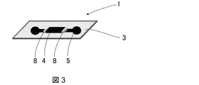
- FIG. 3 shows the electronic device 1 in which a conductive wiring 5 electrically connected to the electronic element 4 is further formed on the polymer nanosheet 3 with respect to the electronic device 1 of FIG. Since the polymer nanosheet 3 physically adheres and follows the electronic element 4, the electronic element 4 is strongly bonded to the polymer nanosheet 3 by intermolecular force. At this time, when the electrode 8 of the electronic element 4 is arranged on the conductive wiring 5 on the polymer nanosheet 3, the conductive wiring 5 and the electrode 8 are pressure-bonded, and molecules between the conductive wiring 5 and the electrode 8 are pressed. Interactivity is also strengthened. Thereby, the conductive wiring 5 can be connected to the electrode 8 of the electronic element 4 with a strong adhesive force, and the conductive wiring 5 can be electrically connected to the electronic element 4 without performing soldering or the like.
- Examples of the electronic element 4 include light-emitting elements such as light-emitting diodes (LEDs), active parts such as transistors, diodes, and ICs, and passive parts such as resistors, inductors, and capacitors.
- the electronic device 1 can be manufactured by bringing various sensors such as a strain sensor or an RFID tag into close contact with the polymer nanosheet 3.
- FIG. 4 shows the electronic device 1 in which a power source 7 for supplying power to the active component 6 as the electronic element 4 is further arranged on the polymer nanosheet 3 with respect to the electronic device 1 of FIG.
- a power source 7 for supplying power to the active component 6 as the electronic element 4 is further arranged on the polymer nanosheet 3 with respect to the electronic device 1 of FIG.
- the electronic device 1 that is integrally provided with the power source 7 that supplies power to the active component 6.
- the power source 7 a battery such as a solar battery or a capacitor battery using a large-capacity capacitor can be used.
- the power source 7 may supply power to the electronic element 4 with an induction coil used in a non-contact IC card.
- the polymer nanosheet 3 used in the present invention for example, a polymer such as a synthetic polymer, a natural polymer, rubber, or elastomer can be used as a material. More specifically, the polymer nanosheet 3 has polystyrene isoprene styrene, polydimethylsiloxane, silicone, polystyrene, polymethacrylic acid, polylactic acid, polylactic acid glycolic acid copolymer, polyvinyl acetate, chitosan, alginic acid, cellulose acetate, It is preferably made of any one of hyaluronic acid, gelatin, and collagen.
- a substrate 11 for forming a polymer nanosheet 3 or the like thereon is prepared.
- the substrate 11 is separated from the polymer nanosheet 3 when the electronic device 1 is attached to the attachment object 2 such as skin.
- PET polyethylene terephthalate
- PP polypropylene
- PPE polyphenylene ether
- COP cycloolefin
- PI polyimide
- aluminum foil conductive polymer film, paper, polysaccharide film, silicone resin Oblate (gelatin), silicon wafer, glass and the like
- a PET film Limirror 25T60, manufactured by Panac
- the sacrificial layer 12 is formed on the substrate 11.
- the sacrificial layer 12 is used to separate the substrate 11 from the polymer nanosheet 3 after the polymer nanosheet 3 is formed.
- the film forming method may be based on a roll-to-roll technique using a gravure coater (not shown), or using a spin coater (not shown). In the roll-to-roll technique, a film can be formed in a larger area than when a spin coater is used. In the present embodiment, film formation was performed using a gravure coater (ML-120, manufactured by Yurai Seiki Co., Ltd.).
- the rotation speed was 30 rpm
- the linear velocity was 1.3 m / min
- the drying temperature was 100 ° C.
- water-soluble polyvinyl alcohol PVA, manufactured by Kanto Chemical Co., Inc., 2 wt% in water
- the polymer nanosheet 3 is formed on the sacrificial layer 12 to form the polymer nanosheet substrate 13 including the substrate 11, the sacrificial layer 12, and the polymer nanosheet 3.
- the thickness of the polymer nanosheet 3 is preferably less than 1 ⁇ m.
- the followability to the pasting object 2 such as skin is high, and the adhesion can be improved.
- the film thickness is 250 nm or less, the followability is higher and the adhesion is also improved.
- the film thickness is 1 ⁇ m or more, the followability to the electronic element 4 and the pasting object 2 is inferior.
- the polymer nanosheet 3 can be formed using a roll-to-roll technique using a gravure coater (not shown) or a film forming method such as a spin coater, as with the sacrificial layer 12 described above.
- a gravure coater not shown
- a film forming method such as a spin coater
- the film-forming method used was a roll-to-roll technique using a gravure coater, and the film-forming conditions were a rotation speed of 30 rpm, a linear velocity of 1.3 m / min, and a drying temperature of 100 ° C.
- the conductive material 23 is ejected onto the polymer nanosheet 3 by ink jet, and the conductive wiring 5 is formed on the polymer nanosheet 3 as shown in FIG. 6B.
- an ink jet printer (DCP-J540N, manufactured by Brother Industries, Ltd.) (not shown) is used, and silver nanoparticles 21 (Drycure Ag-J 4 mPa ⁇ s, manufactured by Colloidal Inc., particle size 15 nm ⁇ )
- a wiring pattern consisting of was drawn on the surface of the polymer nanosheet 3.
- the conductive wiring 5 As a material for forming the conductive wiring 5, for example, at least one of metal nanoparticles, semiconductor nanoparticles, conductive polymers, and nanocarbon materials can be used. In particular, it is preferable to use metal nanoparticles such as silver, gold, copper, or nickel because a material that is relatively easily available and has a low resistivity can be used. Further, as a method for forming a wiring pattern, the conductive wiring 5 can be formed on the polymer nanosheet 3 by using a simple method such as offset printing or screen printing in addition to the above-described inkjet printing.
- a frame 22 made of paper tape is provided around the polymer nanosheet substrate 13 on which the conductive wiring 5 of FIG. 6B is printed, and is immersed in a stripping solution 16 made of water, for example.
- a stripping solution 16 made of water, for example.
- the electronic device 1 can be manufactured by bringing the electronic element 4 into close contact with the polymer nanosheet 3 and making electrical connection with the conductive wiring 5.
- an ink receiving layer 14 may be further formed on the polymer nanosheet substrate 13 before the conductive wiring 5 is printed.
- chitosan, polyvinyl acetate, cellulose acetate, gelatin, silica, and a cationic acrylic copolymer are desirable.
- the fine conductive wiring 5 can be formed more accurately without the ink containing the conductive material 23 being repelled.
- a cationic acrylic copolymer (NS-600X, manufactured by Takamatsu Yushi Co., Ltd.) was used as the ink receiving layer 14.
- the film forming method uses a roll-to-roll technique using a gravure coater as in the case of the sacrificial layer 12 and the polymer nanosheet 3 described above.
- the film forming conditions include a rotation speed of 30 rpm and a linear velocity of 1.3 m / min.
- the drying temperature was 100 ° C.
- the sacrificial layer 12 is not necessarily formed.
- a combination of the substrate 11 and the polymer nanosheet 3 that does not have very good adhesion, and a frame made of paper tape formed around the polymer nanosheet substrate 13 is used. It is also possible to separate the molecular nanosheet 3 from the substrate 11.
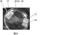
- FIG. 8 shows a self-supporting polymer nanosheet 3 formed by immersing the above-described polymer nanosheet substrate 13 in water 16 to dissolve the PVA layer as the sacrificial layer 12 and separating the PET film as the substrate 11.
- a photograph of the SBS nanosheet 15 is shown. The figure shows a state in which paper 17 is bonded to both sides of the SBS nanosheet 15 and the SBS nanosheet 15 is extended with tweezers.
- the SBS nanosheet 15 was prepared by changing the concentration of the SBS solution, and the peeled SBS nanosheet 15 was pasted on a smooth silicon substrate and the film thickness was measured using an atomic force microscope (AFM). It was confirmed that the film thickness increased.
- the prepared SBS nanosheet 15 showed high stretchability, and showed an elastic modulus (40 MPa, film thickness 212 nm) about 20 times lower than that of a nanosheet made of polystyrene which is one of the constituent units of SBS.
- FIG. 9 and 10 show that the surface mount type LED 26 (1.5 mm ⁇ 3.0 mm ⁇ 0.6 mm) as the electronic element 4 is arranged on the polymer nanosheet 3 on which the conductive wiring 5 is printed. It is the photograph which showed that LED26 light-emitted electrically fixed.
- FIG. 9 is a photograph observed from the side where the LED 26 is arranged, and
- FIG. 10 is a photograph observed from the back side. From these photographs, it was confirmed that the conductive wiring 5 flexibly follows the electrode portion 27 of the LED 26.
- the side on which the electronic element 4 is disposed is used as a front surface, and the polymer nanosheet 3 is pasted on the object 2 to be pasted, whereas the side on which the electronic element 4 is disposed is on the object to be pasted 2 side. You may make it stick.
- the surface where the electronic element 4 was covered with the polymer nanosheet 3 becomes a front surface, the electronic element 4 can be protected from the outside.
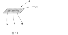
- FIG. 11 is a schematic diagram of the electronic device 1 according to the present embodiment
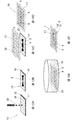
- FIG. 12 is a schematic diagram illustrating an example of the manufacturing process of the electronic device 1
- FIGS. 13 to 17 are diagrams from the silver nanoparticles 21 manufactured in the present embodiment.
- FIG. 18 to FIG. 23 are photographs showing the electronic device 1 actually manufactured
- FIG. 18 to FIG. 23 are diagrams showing characteristics evaluation results of the polymer nanosheet 3 having the conductive wiring 5.
- the basic configuration in which the electronic element 4, the conductive wiring 5, and the power source 7 are arranged on the polymer nanosheet 3 is the same as that in the first embodiment.
- the first embodiment has a structure in which the electronic element 4 or the like is disposed on the first polymer nanosheet 31 and the first polymer nanosheet 31 and the second polymer nanosheet 32 are adhered and bonded together.
- the electronic element 4 is different in that it is sandwiched between the first polymer nanosheet 31 and the second polymer nanosheet 32.
- the electronic element 4 and the conductive wiring 5 are arranged on the first polymer nanosheet 31.
- a power source 7 may be arranged. In this way, by sandwiching the electronic element 4 and the like between the two first polymer nanosheets 31 and the second polymer nanosheet 32, the polymer nanosheet (the first polymer nanosheet 31 and the second polymer nanosheet 32) and the electronic element 4 and the electronic element 4 can be physically protected from the outside.
- the thicknesses of the first polymer nanosheet 31 and the second polymer nanosheet 32 are preferably less than 1 ⁇ m.
- the materials of the first polymer nanosheet 31 and the second polymer nanosheet 32 are also polystyrene isoprene styrene, polydimethylsiloxane, silicone, polystyrene, polymethacrylic acid, polylactic acid, polylactic acid glycolic acid copolymer, polyvinyl acetate, respectively. , Chitosan, alginic acid, cellulose acetate, hyaluronic acid, gelatin, and collagen.
- FIG. 12A and FIG. 12B is the same as the process shown in FIG. 6A and FIG. 6B of Embodiment 1, and FIG. FIG. 12B shows the conductive wiring 5 formed on the first polymer nanosheet 31 of the polymer nanosheet substrate 13.
- the electronic element 4 is disposed on the first polymer nanosheet 31 on which the conductive wiring 5 is printed, and the electronic element 4 is brought into close contact with the first polymer nanosheet 31 and electrically connected to the conductive wiring 5.
- a second polymer nanosheet 32 to be bonded to the first polymer nanosheet 31 is prepared.
- the second polymer nanosheet 32 is provided with a frame 17 made of paper tape around it.
- the 1st polymer nanosheet 31 and the 2nd polymer nanosheet 32 are bonded together, and the polymer nanosheet bonding base
- FIGS. 12E and 12F are the same as the steps shown in FIGS. 6C and 6D of the first embodiment.
- the polymer nanosheet bonding substrate 33 of FIG. 12D is immersed in a stripping solution 16 made of, for example, water.
- a stripping solution 16 made of, for example, water.
- the sacrificial layer 12 is dissolved, and the substrate 11 is separated from the first polymer nanosheet 31, and the electronic device 1 shown in FIG. 12F can be manufactured.
- the step of forming the sacrificial layer 12 can be omitted.
- the sacrificial layer 12 is provided by combining the substrate 11 and the first polymer nanosheet 31 so that the adhesion is not so good and using a frame made of paper tape formed around the second polymer nanosheet 32.
- the first polymer nanosheet 31 can be separated from the substrate 11.
- the electronic device 1 of the present embodiment has a structure in which the electronic element 4 is sandwiched between the first polymer nanosheet 31 and the second polymer nanosheet 32, and the method for manufacturing the electronic device 1 as described above. Therefore, the electronic device 1 using the polymer nanosheet 3 can be manufactured by a simple process.
- the ink receiving layer 14 is further provided on at least one of the first polymer nanosheet 31 and the second polymer nanosheet 32, and the conductive wiring 5 is provided in the ink receiving layer 14. You may make it print on top.
- the cationic ink receiving layer 14 (film thickness: 115 ⁇ 26 nm) is formed on the surface of the SBS nanosheet 15 (film thickness: 383 ⁇ 21 nm) as the first polymer nanosheet 31 formed on the PET film as the substrate 11. Filmed.
- conductive wiring 5 (thickness 159 ⁇ 55 nm, line width:> 0.37 mm) made of silver nanoparticles 21 was formed using ink jet printing.
- SEM scanning electron microscope
- the resistance value decreased by 3 digits or more as shown in FIG.
- the resistance value is significantly reduced in the heat treatment at 100 ° C. or higher.
- the sheet resistance was found to decrease from 1.22 ⁇ 10 4 ⁇ / sq before the heat treatment to 10.5 ⁇ / sq.
- the change in resistance value of the conductive wiring 5 when the SBS nanosheet 15 was stretched and returned using the stretchability of the SBS nanosheet 15 was measured, and as shown in FIG. Even in the case of reversible resistance value change. From the above, it was confirmed that the SBS nanosheet 15 having the conductive wiring 5 is excellent in conductivity and stretchability. From such characteristics, the SBS nanosheet 15 having the conductive wiring 5 is expected to be applied as an electronic device 1 such as a circuit board or a strain gauge.
- the resistance measurement described above is performed in accordance with the present embodiment, and the conductive wiring 5 is formed with the first polymer nanosheet 31 and the second polymer nanosheet 32 (the SBS nanosheet similar to the first polymer nanosheet 31). This is done using a sample that is sandwiched. However, when used as a circuit board or a strain gauge as described above, it is also possible to use a single-layer nanosheet as in the first embodiment.
- FIG. 18 shows another surface-mounted LED 26 similar to that of the first embodiment disposed on the first polymer nanosheet 31 made of SBS on which the conductive wiring 5 is printed, and the surface thereof is another second polymer nanosheet made of SBS.
- the LED 26 is physically and electrically fixed.
- the conductive wiring 5 and the LED 26 are observed from the back side of the polymer nanosheet 3 made of these closely contacted SBS, it is confirmed that the conductive wiring 5 flexibly follows the electrode portion 27 of the LED 26 as shown in FIG. It was.
- the LED 26 sandwiched between the first polymer nanosheet 31 and the second polymer nanosheet 32 emits light without chemical bonding such as soldering.
- the sticking property to the skin surface as the sticking object 2 and the operability of the LED 26 were verified.
- the electronic device 1 could be attached to the skin surface without causing cracks.
- the conductive wire 37 was pulled out from the electronic device 1 and a 3V battery was connected, it was confirmed that two LEDs 26 were lit on the skin.
- the conductive wiring 5 followed to the inside of the skin groove 36, and the high followability of the polymer nanosheet 3 made of SBS was shown.
- FIG. 24 is a schematic view showing a manufacturing process of the jumper wiring 47 using the polymer nanosheet 41 of the present embodiment
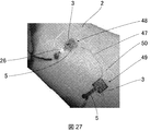
- FIGS. 25 to 27 are photographs of the actually manufactured jumper wiring 47, the composite electronic device 50, and the like. .
- a non-conductive polymer nanosheet 41 is immersed in water.
- the both ends of the conductive yarn 43 are brought close to the polymer nanosheet 41 in the water 42 while being held by, for example, tweezers 44.
- the polymer nanosheet can be covered with the conductive yarn 43 so as to be wound around the conductive yarn 43 as shown in FIG. 24C.
- the jumper wiring 47 divided into the conductive regions 45 at both ends of the conductive yarn 43 and the non-conductive region 46 in which the polymer nanosheet 41 is coated around the conductive yarn 43. can be produced.
- a conductive yarn made of silver fiber (AGPOSS twisted yarn, manufactured by Mitsuji Textile Industry Co., Ltd.) was used as the conductive yarn 43.
- FIG. 25 shows the conductive thread 43 before coating with the polymer nanosheet
- FIG. 26 shows the non-conductive region 46 in which the conductive thread 43 is coated with the polymer nanosheet 3 made of polylactic acid.
- This jumper wiring 47 can be bonded onto the polymer nanosheet 3 having the conductive wiring 5 of the first and second embodiments, for example.
- the first electronic device 48 in which the LED 26 is mounted on the polymer nanosheet 3 and the second electronic device 49 having the conductive wiring 5 on the polymer nanosheet 3 are electrically connected by the jumper wiring 47, and the voltage It is verified that the lighting of the LED 26 is confirmed by applying the voltage to make the LED 26 conductive.
- a plurality of electronic devices 48 and 49 arranged physically and electrically separated can be electrically connected by jumper wiring 47 covered with polymer nanosheet 41 to form composite electronic device 50. it can.
- the electronic element 4 is adhered to the polymer sheet 3 having a film thickness of less than 1 ⁇ m by intermolecular force, and the skin or the like. It is possible to provide the electronic device 1 that can be attached to the sticking object 2 with high followability without using glue or the like.
- the electronic device 1 on which the active component 6 is mounted can be realized without using any soldering or the like.
- the fine conductive wiring 5 can be formed more accurately without the ink containing the conductive material 23 being repelled.
- the polymer nanosheet 3 and the electron can be obtained by sandwiching the electronic element 4 and the like between the first polymer nanosheet 31 and the second polymer nanosheet 32.
- the adhesion between the device 4 and the electronic device 4 can be physically protected from the outside.
- the conductive yarn 43 is covered with the non-conductive polymer nanosheet 41 to form the jumper wiring 47 having the conductive region 45 and the non-conductive region 46, and the physical A plurality of electronic devices 48 and 49 arranged separately from each other electrically are electrically connected by the jumper wiring 47 to form a composite electronic device 50 formed by the plurality of electronic devices 48 and 49. can do.
- the material of the polymer nanosheet 3 is not limited to those exemplified in the above embodiment, and various materials can be applied as long as the polymer nanosheet 3 can adhere the electronic element 4 and the like by intermolecular force.
- Various materials can be applied to the material 5 as long as it is a conductive material.
- the method for forming the conductive wiring 5 is not limited to printing.
- the power source 7 is preferably formed on the polymer nanosheet 3 or between the first polymer nanosheet 31 and the second polymer nanosheet 32, but is provided outside the electronic device 1, and is provided inside the electronic device 1. You may make it connect with the conductive wiring 5.
- the electronic device 1 is capable of measuring a pulse rate and skin conductance or performing perspiration detection by being affixed to an object to be affixed such as skin or an organ. It can be used as an electronic device 1 for medical use and as an electronic device 1 for biological monitoring of sports athletes. Further, for example, by using an RFID tag as the electronic element 4, it is possible to check the entrance gate for a visitor who has attached the electronic device 1 to the skin or the like, and substitute the ticket function. Furthermore, the present invention can be applied to an ecological survey by attaching the electronic device 1 to an organ or an animal other than a human being or an insect and tracking its position information. In addition, the present invention can be applied to the traceability of products by pasting the electronic device 1 storing information such as a production location and a producer on a product such as food.
Landscapes
- Engineering & Computer Science (AREA)
- Microelectronics & Electronic Packaging (AREA)
- Life Sciences & Earth Sciences (AREA)
- Health & Medical Sciences (AREA)
- Physics & Mathematics (AREA)
- Theoretical Computer Science (AREA)
- General Health & Medical Sciences (AREA)
- Animal Behavior & Ethology (AREA)
- Manufacturing & Machinery (AREA)
- Veterinary Medicine (AREA)
- Biophysics (AREA)
- Pathology (AREA)
- Biomedical Technology (AREA)
- Heart & Thoracic Surgery (AREA)
- Medical Informatics (AREA)
- Molecular Biology (AREA)
- Surgery (AREA)
- Public Health (AREA)
- Computer Hardware Design (AREA)
- General Physics & Mathematics (AREA)
- Human Computer Interaction (AREA)
- General Engineering & Computer Science (AREA)
- Non-Metallic Protective Coatings For Printed Circuits (AREA)
- Electric Connection Of Electric Components To Printed Circuits (AREA)
- Laminated Bodies (AREA)
- Parts Printed On Printed Circuit Boards (AREA)
- Led Device Packages (AREA)
Abstract
Description
T. Fujie and S. Takeoka, in Nanobiotechnology, eds. D. A. Phoenix and A. Waqar, One Central Press, United Kingdom, 2014, pp. 68-94.
3 高分子ナノシート
4 電子素子
5 導電配線
6 能動部品
7 電源
8 電極
11 基板
12 犠牲層
14 インク受容層
21 銀ナノ粒子
31 第1高分子ナノシート
32 第2高分子ナノシート
Claims (17)
- 電子素子と、
前記電子素子に密着した高分子ナノシートと
を含むことを特徴とする電子デバイス。 - 前記高分子ナノシートは、前記電子素子の1面全体を覆うように密着していることを特徴とする請求項1記載の電子デバイス。
- 前記高分子ナノシートの厚さが1μm未満であることを特徴とする請求項1または2に記載の電子デバイス。
- 前記高分子ナノシート上に前記電子素子と電気的に接続する導電配線が形成されていることを特徴とする請求項1~3のいずれか1項に記載の電子デバイス。
- 前記高分子ナノシート上にインク受容層をさらに備え、前記導電配線が前記インク受容層上に印刷されて形成されたものであることを特徴とする請求項4記載の電子デバイス。
- 前記電子素子は能動部品であり、前記能動部品に電力を供給する電源が、前記高分子ナノシート上にさらに配置されることを特徴とする請求項4または5に記載の電子デバイス。
- 前記高分子ナノシートが、ポリスチレンイソプレンスチレン、ポリジメチルシロキサン、シリコーン、ポリスチレン、ポリメタクリル酸、ポリ乳酸、ポリ乳酸グリコール酸共重合体、ポリ酢酸ビニル、キトサン、アルギン酸、酢酸セルロース、ヒアルロン酸、ゼラチン、および、コラーゲンのうちのいずれか一つからなることを特徴とする請求項1~6のいずれか1項に記載の電子デバイス。
- 前記高分子ナノシートは、第1高分子ナノシートと第2高分子ナノシートとが密着して貼り合わされた構造からなり、前記電子素子は、前記第1高分子ナノシートと前記第2高分子ナノシートとの間に挟み込まれていることを特徴とする請求項2記載の電子デバイス。
- 前記第1高分子ナノシートおよび前記第2高分子ナノシートの厚さがそれぞれ1μm未満であることを特徴とする請求項8記載の電子デバイス。
- 前記第1高分子ナノシートおよび前記第2高分子ナノシートの少なくとも一方の高分子ナノシート上に前記電子素子と電気的に接続する導電配線が形成されていることを特徴とする請求項8または9に記載の電子デバイス。
- 前記第1高分子ナノシートおよび前記第2高分子ナノシートの少なくとも一方の高分子ナノシート上にインク受容層をさらに備え、前記導電配線が前記インク受容層上に印刷されて形成されたものであることを特徴とする請求項10記載の電子デバイス。
- 前記電子素子は能動部品であり、前記能動部品に電力を供給する電源が、前記第1高分子ナノシートと前記第2高分子ナノシートとの間にさらに挟み込まれることを特徴とする請求項10または11記載の電子デバイス。
- 前記第1高分子ナノシートおよび前記第2高分子ナノシートが、それぞれポリスチレンイソプレンスチレン、ポリジメチルシロキサン、シリコーン、ポリスチレン、ポリメタクリル酸、ポリ乳酸、ポリ乳酸グリコール酸共重合体、ポリ酢酸ビニル、キトサン、アルギン酸、酢酸セルロース、ヒアルロン酸、ゼラチン、および、コラーゲンのうちのいずれか一つからなることを特徴とする請求項8~12のいずれか1項に記載の電子デバイス。
- 前記導電配線が、金属ナノ粒子、半導体ナノ粒子、導電性高分子、および、ナノ炭素材料のうちの少なくとも一つからなることを特徴とする請求項4~7および10~13のいずれか1項に記載の電子デバイス。
- 前記金属ナノ粒子が、銀、金、銅、および、ニッケルのうちの少なくとも一つであることを特徴とする請求項14に記載の電子デバイス。
- 基板上に第1高分子ナノシートを形成するステップと、
前記第1高分子ナノシート上に導電配線を形成するステップと、
前記導電配線に電子素子の電極が接するように前記電子素子を配置するステップと、
第2高分子ナノシートを、前記電子素子および前記導電配線を前記第1高分子ナノシートとの間に挟み込むようにして前記第1高分子ナノシートに密着して貼り合わせ、前記電子素子および前記導電配線を電気的に接続するステップと、
前記第1高分子ナノシートから前記基板を分離するステップと
を含むことを特徴とする電子デバイスの製造方法。 - 前記第1高分子ナノシートを形成するステップにおいて、前記基板上に前記第1および第2高分子ナノシートを溶解しない溶剤で溶解可能な犠牲層を形成した後に、前記犠牲層上に前記第1高分子ナノシートを形成し、前記基板を分離するステップにおいて、前記犠牲層を前記溶剤で溶解して前記第1高分子ナノシートから前記基板を分離することを特徴とする請求項16に記載の電子デバイスの製造方法。
Priority Applications (2)
| Application Number | Priority Date | Filing Date | Title |
|---|---|---|---|
| JP2017517947A JP6773332B2 (ja) | 2015-05-11 | 2016-05-10 | 電子デバイスおよびその製造方法 |
| US15/573,297 US10474188B2 (en) | 2015-05-11 | 2016-05-10 | Flexible electronic device containing electronic element and polymer nanosheet and method for manufacturing same |
Applications Claiming Priority (2)
| Application Number | Priority Date | Filing Date | Title |
|---|---|---|---|
| JP2015096887 | 2015-05-11 | ||
| JP2015-096887 | 2015-05-11 |
Publications (1)
| Publication Number | Publication Date |
|---|---|
| WO2016181958A1 true WO2016181958A1 (ja) | 2016-11-17 |
Family
ID=57248187
Family Applications (1)
| Application Number | Title | Priority Date | Filing Date |
|---|---|---|---|
| PCT/JP2016/063841 Ceased WO2016181958A1 (ja) | 2015-05-11 | 2016-05-10 | 電子デバイスおよびその製造方法 |
Country Status (3)
| Country | Link |
|---|---|
| US (1) | US10474188B2 (ja) |
| JP (1) | JP6773332B2 (ja) |
| WO (1) | WO2016181958A1 (ja) |
Cited By (3)
| Publication number | Priority date | Publication date | Assignee | Title |
|---|---|---|---|---|
| WO2020246539A1 (ja) * | 2019-06-04 | 2020-12-10 | 学校法人早稲田大学 | バッテリレス電子デバイス及び伝送システム |
| WO2023063070A1 (ja) | 2021-10-13 | 2023-04-20 | 国立大学法人東京工業大学 | 脳表に貼付して使用される記録及び/又は刺激用の神経電極とそれを用いた記録又は刺激方法 |
| WO2025187550A1 (ja) * | 2024-03-05 | 2025-09-12 | 国立大学法人横浜国立大学 | 放熱シート、放熱シートの製造方法 |
Families Citing this family (9)
| Publication number | Priority date | Publication date | Assignee | Title |
|---|---|---|---|---|
| WO2018098409A1 (en) * | 2016-11-28 | 2018-05-31 | Med-El Elektromedizinische Geraete Gmbh | Respiration monitoring sensor for a laryngeal pacemaker |
| KR102225172B1 (ko) * | 2019-04-05 | 2021-03-09 | 재단법인대구경북과학기술원 | 나노섬유 메쉬 습도센서 및 이의 제조방법 |
| EP4003501B1 (en) * | 2019-07-31 | 2026-01-21 | Med-El Elektromedizinische Geraete GmbH | Printed tattoo electrode respiration sensor for laryngeal pacemakers |
| EP4022674A2 (en) * | 2019-08-26 | 2022-07-06 | X-Celeprint Limited | Variable stiffness modules |
| US12288736B2 (en) | 2019-11-28 | 2025-04-29 | Prevayl Innovations Limited | Sensor package, article comprising the same and manufacturing method thereof |
| GB2589568B (en) | 2019-11-28 | 2025-10-10 | Prevayl Innovations Ltd | Sensor device, system and wearable article |
| GB2589567B (en) * | 2019-11-28 | 2024-07-10 | Prevayl Innovations Ltd | Semiconductor package, article and method |
| GB2589359A (en) | 2019-11-28 | 2021-06-02 | Prevayl Ltd | Sensor device, system and wearable article |
| US12343166B2 (en) | 2020-02-26 | 2025-07-01 | Prevayl Innovations Limited | Signal measuring apparatus and system |
Citations (2)
| Publication number | Priority date | Publication date | Assignee | Title |
|---|---|---|---|---|
| JP2010155919A (ja) * | 2008-12-26 | 2010-07-15 | National Institute Of Advanced Industrial Science & Technology | ポリイミド薄膜の作製方法 |
| JP2010161118A (ja) * | 2009-01-06 | 2010-07-22 | Ube Nitto Kasei Co Ltd | 多孔質膜、多孔質膜形成用塗工液、その製造方法、積層基板および配線材料 |
Family Cites Families (7)
| Publication number | Priority date | Publication date | Assignee | Title |
|---|---|---|---|---|
| US7730610B2 (en) * | 2005-09-29 | 2010-06-08 | Panasonic Corporation | Method of mounting electronic circuit constituting member and relevant mounting apparatus |
| JP4306795B2 (ja) * | 2007-05-18 | 2009-08-05 | 凸版印刷株式会社 | 配線基板、半導体パッケージ、電子機器及び配線基板の製造方法 |
| JP5830381B2 (ja) * | 2009-10-13 | 2015-12-09 | ナノシータ株式会社 | 高分子超薄膜分散体及びその調製方法 |
| DK2592915T3 (da) * | 2010-07-06 | 2022-04-19 | Fujikura Ltd | Fremstillingsfremgangsmåde til lamineret printplade |
| JP2012069673A (ja) | 2010-09-22 | 2012-04-05 | Sony Corp | フレキシブル基板、フレキシブル基板の実装方法及び照明装置 |
| JP2013258209A (ja) | 2012-06-11 | 2013-12-26 | Nitto Denko Corp | 封止シート、発光ダイオード装置およびその製造方法 |
| US10006141B2 (en) * | 2013-06-20 | 2018-06-26 | Baker Hughes, A Ge Company, Llc | Method to produce metal matrix nanocomposite |
-
2016
- 2016-05-10 WO PCT/JP2016/063841 patent/WO2016181958A1/ja not_active Ceased
- 2016-05-10 JP JP2017517947A patent/JP6773332B2/ja not_active Expired - Fee Related
- 2016-05-10 US US15/573,297 patent/US10474188B2/en not_active Expired - Fee Related
Patent Citations (2)
| Publication number | Priority date | Publication date | Assignee | Title |
|---|---|---|---|---|
| JP2010155919A (ja) * | 2008-12-26 | 2010-07-15 | National Institute Of Advanced Industrial Science & Technology | ポリイミド薄膜の作製方法 |
| JP2010161118A (ja) * | 2009-01-06 | 2010-07-22 | Ube Nitto Kasei Co Ltd | 多孔質膜、多孔質膜形成用塗工液、その製造方法、積層基板および配線材料 |
Non-Patent Citations (1)
| Title |
|---|
| KENSHI NUMAKURA: "Yoku Wakaru Flexible Electronics no Dekiru made", 22 December 2010 (2010-12-22), pages 33, 78, 120, 144 * |
Cited By (3)
| Publication number | Priority date | Publication date | Assignee | Title |
|---|---|---|---|---|
| WO2020246539A1 (ja) * | 2019-06-04 | 2020-12-10 | 学校法人早稲田大学 | バッテリレス電子デバイス及び伝送システム |
| WO2023063070A1 (ja) | 2021-10-13 | 2023-04-20 | 国立大学法人東京工業大学 | 脳表に貼付して使用される記録及び/又は刺激用の神経電極とそれを用いた記録又は刺激方法 |
| WO2025187550A1 (ja) * | 2024-03-05 | 2025-09-12 | 国立大学法人横浜国立大学 | 放熱シート、放熱シートの製造方法 |
Also Published As
| Publication number | Publication date |
|---|---|
| US10474188B2 (en) | 2019-11-12 |
| JP6773332B2 (ja) | 2020-10-21 |
| JPWO2016181958A1 (ja) | 2018-03-29 |
| US20180107244A1 (en) | 2018-04-19 |
Similar Documents
| Publication | Publication Date | Title |
|---|---|---|
| JP6773332B2 (ja) | 電子デバイスおよびその製造方法 | |
| Zhang et al. | Conformal manufacturing of soft deformable sensors on the curved surface | |
| CN106908176B (zh) | 具有微结构化的多相介电层电容式压力传感器及其制法 | |
| US9247637B2 (en) | Strain relief structures for stretchable interconnects | |
| Pang et al. | Recent advances in flexible sensors for wearable and implantable devices | |
| US12114982B2 (en) | Skin-mountable electronic devices and methods of using and fabricating the same | |
| Du et al. | A review of inkjet printing technology for personalized-healthcare wearable devices | |
| US12465259B2 (en) | Thin film support structures | |
| US10098223B2 (en) | Sensor device with a flexible electrical conductor structure | |
| CA2900700A1 (en) | Strain relief structures for stretchable interconnects | |
| CN104582246B (zh) | 电磁波屏蔽膜以及带电磁波屏蔽膜的柔性印刷电路板 | |
| CN114980812A (zh) | 生物体用电极、其制造方法及佩戴方法 | |
| US20220340726A1 (en) | Gas permeable, ultrathin, stretchable epidermal electronic devices and related methods | |
| Kim et al. | Stretching silver: printed metallic nano inks in stretchable conductor applications | |
| Eshkeiti et al. | A stretchable and wearable printed sensor for human body motion monitoring | |
| CN106953001A (zh) | 一种基于碳纳米管薄膜及光刻胶的柔性压力传感器及其制备方法 | |
| JP5799184B1 (ja) | 透明導電積層体およびその製造方法 | |
| JP2010050173A5 (ja) | ||
| Oh et al. | Dual-functional self-attachable and stretchable interface for universal three-dimensional modular electronics | |
| US11547338B2 (en) | Electronic functional member, electronic component, and wearable device | |
| Kassanos et al. | Sensor embodiment and flexible electronics | |
| CN205697715U (zh) | 柔性可穿戴装置 | |
| CN109792836A (zh) | 电子装置及其制造方法 | |
| TW201509673A (zh) | 透明導電體 | |
| JP2020061487A (ja) | 電磁波シールドフィルム、電磁波シールドフィルム付きプリント配線板およびその製造方法 |
Legal Events
| Date | Code | Title | Description |
|---|---|---|---|
| 121 | Ep: the epo has been informed by wipo that ep was designated in this application |
Ref document number: 16792683 Country of ref document: EP Kind code of ref document: A1 |
|
| DPE1 | Request for preliminary examination filed after expiration of 19th month from priority date (pct application filed from 20040101) | ||
| ENP | Entry into the national phase |
Ref document number: 2017517947 Country of ref document: JP Kind code of ref document: A |
|
| WWE | Wipo information: entry into national phase |
Ref document number: 15573297 Country of ref document: US |
|
| NENP | Non-entry into the national phase |
Ref country code: DE |
|
| 122 | Ep: pct application non-entry in european phase |
Ref document number: 16792683 Country of ref document: EP Kind code of ref document: A1 |